JP5882510B2 - Photosensitive dry film and method for producing printed wiring board using the same - Google Patents
Photosensitive dry film and method for producing printed wiring board using the same Download PDFInfo
- Publication number
- JP5882510B2 JP5882510B2 JP2015025558A JP2015025558A JP5882510B2 JP 5882510 B2 JP5882510 B2 JP 5882510B2 JP 2015025558 A JP2015025558 A JP 2015025558A JP 2015025558 A JP2015025558 A JP 2015025558A JP 5882510 B2 JP5882510 B2 JP 5882510B2
- Authority
- JP
- Japan
- Prior art keywords
- film
- photosensitive resin
- photosensitive
- dry film
- compound
- Prior art date
- Legal status (The legal status is an assumption and is not a legal conclusion. Google has not performed a legal analysis and makes no representation as to the accuracy of the status listed.)
- Active
Links
- 238000004519 manufacturing process Methods 0.000 title claims description 11
- 229920005989 resin Polymers 0.000 claims description 150
- 239000011347 resin Substances 0.000 claims description 150
- -1 isocyanate compound Chemical class 0.000 claims description 116
- 239000011342 resin composition Substances 0.000 claims description 69
- 150000001875 compounds Chemical class 0.000 claims description 49
- 229910000679 solder Inorganic materials 0.000 claims description 33
- 238000000576 coating method Methods 0.000 claims description 28
- 239000000758 substrate Substances 0.000 claims description 28
- 230000003746 surface roughness Effects 0.000 claims description 28
- 239000011248 coating agent Substances 0.000 claims description 25
- 238000000034 method Methods 0.000 claims description 24
- 229920001187 thermosetting polymer Polymers 0.000 claims description 22
- 239000004593 Epoxy Substances 0.000 claims description 21
- 230000001681 protective effect Effects 0.000 claims description 18
- 239000012948 isocyanate Substances 0.000 claims description 17
- 239000000945 filler Substances 0.000 claims description 14
- 229920005992 thermoplastic resin Polymers 0.000 claims description 13
- 238000011161 development Methods 0.000 claims description 10
- 239000000853 adhesive Substances 0.000 claims description 6
- 230000001070 adhesive effect Effects 0.000 claims description 6
- 150000003553 thiiranes Chemical class 0.000 claims description 6
- 229920003180 amino resin Polymers 0.000 claims description 5
- CMLFRMDBDNHMRA-UHFFFAOYSA-N 2h-1,2-benzoxazine Chemical compound C1=CC=C2C=CNOC2=C1 CMLFRMDBDNHMRA-UHFFFAOYSA-N 0.000 claims description 2
- 150000001718 carbodiimides Chemical class 0.000 claims description 2
- 125000003178 carboxy group Chemical group [H]OC(*)=O 0.000 description 74
- 239000003822 epoxy resin Substances 0.000 description 35
- 229920000647 polyepoxide Polymers 0.000 description 35
- 230000000052 comparative effect Effects 0.000 description 32
- 125000002887 hydroxy group Chemical group [H]O* 0.000 description 25
- 239000000049 pigment Substances 0.000 description 25
- 229920001400 block copolymer Polymers 0.000 description 22
- 125000004432 carbon atom Chemical group C* 0.000 description 22
- 239000003999 initiator Substances 0.000 description 19
- 238000011156 evaluation Methods 0.000 description 18
- 125000000217 alkyl group Chemical group 0.000 description 17
- 239000002981 blocking agent Substances 0.000 description 16
- YXFVVABEGXRONW-UHFFFAOYSA-N Toluene Chemical compound CC1=CC=CC=C1 YXFVVABEGXRONW-UHFFFAOYSA-N 0.000 description 15
- 238000006243 chemical reaction Methods 0.000 description 15
- 239000000463 material Substances 0.000 description 15
- 239000000126 substance Substances 0.000 description 15
- IISBACLAFKSPIT-UHFFFAOYSA-N bisphenol A Chemical compound C=1C=C(O)C=CC=1C(C)(C)C1=CC=C(O)C=C1 IISBACLAFKSPIT-UHFFFAOYSA-N 0.000 description 14
- RAXXELZNTBOGNW-UHFFFAOYSA-N imidazole Natural products C1=CNC=N1 RAXXELZNTBOGNW-UHFFFAOYSA-N 0.000 description 14
- 239000005056 polyisocyanate Substances 0.000 description 14
- 229920001228 polyisocyanate Polymers 0.000 description 14
- 229920000642 polymer Polymers 0.000 description 14
- VYPSYNLAJGMNEJ-UHFFFAOYSA-N Silicium dioxide Chemical compound O=[Si]=O VYPSYNLAJGMNEJ-UHFFFAOYSA-N 0.000 description 13
- 238000011049 filling Methods 0.000 description 13
- 239000000203 mixture Substances 0.000 description 13
- NIXOWILDQLNWCW-UHFFFAOYSA-M Acrylate Chemical compound [O-]C(=O)C=C NIXOWILDQLNWCW-UHFFFAOYSA-M 0.000 description 12
- 239000003054 catalyst Substances 0.000 description 12
- 229910052757 nitrogen Inorganic materials 0.000 description 12
- 239000000243 solution Substances 0.000 description 12
- 150000008065 acid anhydrides Chemical class 0.000 description 11
- 239000000178 monomer Substances 0.000 description 11
- 229920000139 polyethylene terephthalate Polymers 0.000 description 11
- 239000005020 polyethylene terephthalate Substances 0.000 description 11
- 229920001971 elastomer Polymers 0.000 description 10
- 229920003986 novolac Polymers 0.000 description 10
- ISWSIDIOOBJBQZ-UHFFFAOYSA-N phenol group Chemical group C1(=CC=CC=C1)O ISWSIDIOOBJBQZ-UHFFFAOYSA-N 0.000 description 10
- 239000000047 product Substances 0.000 description 10
- 239000001062 red colorant Substances 0.000 description 10
- KWYUFKZDYYNOTN-UHFFFAOYSA-M Potassium hydroxide Chemical compound [OH-].[K+] KWYUFKZDYYNOTN-UHFFFAOYSA-M 0.000 description 9
- 125000003545 alkoxy group Chemical group 0.000 description 9
- 238000001035 drying Methods 0.000 description 9
- 239000000806 elastomer Substances 0.000 description 9
- 239000012778 molding material Substances 0.000 description 9
- 125000001997 phenyl group Chemical group [H]C1=C([H])C([H])=C(*)C([H])=C1[H] 0.000 description 9
- 230000008569 process Effects 0.000 description 9
- 229920002803 thermoplastic polyurethane Polymers 0.000 description 9
- LFQSCWFLJHTTHZ-UHFFFAOYSA-N Ethanol Chemical compound CCO LFQSCWFLJHTTHZ-UHFFFAOYSA-N 0.000 description 8
- DNIAPMSPPWPWGF-UHFFFAOYSA-N Propylene glycol Chemical compound CC(O)CO DNIAPMSPPWPWGF-UHFFFAOYSA-N 0.000 description 8
- 125000004122 cyclic group Chemical group 0.000 description 8
- XTQHKBHJIVJGKJ-UHFFFAOYSA-N sulfur monoxide Chemical group S=O XTQHKBHJIVJGKJ-UHFFFAOYSA-N 0.000 description 8
- LYCAIKOWRPUZTN-UHFFFAOYSA-N Ethylene glycol Chemical compound OCCO LYCAIKOWRPUZTN-UHFFFAOYSA-N 0.000 description 7
- 239000002253 acid Substances 0.000 description 7
- PYKYMHQGRFAEBM-UHFFFAOYSA-N anthraquinone Natural products CCC(=O)c1c(O)c2C(=O)C3C(C=CC=C3O)C(=O)c2cc1CC(=O)OC PYKYMHQGRFAEBM-UHFFFAOYSA-N 0.000 description 7
- 239000003086 colorant Substances 0.000 description 7
- 229910052802 copper Inorganic materials 0.000 description 7
- 239000010949 copper Substances 0.000 description 7
- 125000004663 dialkyl amino group Chemical group 0.000 description 7
- LNEPOXFFQSENCJ-UHFFFAOYSA-N haloperidol Chemical class C1CC(O)(C=2C=CC(Cl)=CC=2)CCN1CCCC(=O)C1=CC=C(F)C=C1 LNEPOXFFQSENCJ-UHFFFAOYSA-N 0.000 description 7
- 238000010438 heat treatment Methods 0.000 description 7
- IQPQWNKOIGAROB-UHFFFAOYSA-N isocyanate group Chemical group [N-]=C=O IQPQWNKOIGAROB-UHFFFAOYSA-N 0.000 description 7
- 239000007787 solid Substances 0.000 description 7
- 239000001060 yellow colorant Substances 0.000 description 7
- ZWEHNKRNPOVVGH-UHFFFAOYSA-N 2-Butanone Chemical compound CCC(C)=O ZWEHNKRNPOVVGH-UHFFFAOYSA-N 0.000 description 6
- QTWJRLJHJPIABL-UHFFFAOYSA-N 2-methylphenol;3-methylphenol;4-methylphenol Chemical compound CC1=CC=C(O)C=C1.CC1=CC=CC(O)=C1.CC1=CC=CC=C1O QTWJRLJHJPIABL-UHFFFAOYSA-N 0.000 description 6
- VEXZGXHMUGYJMC-UHFFFAOYSA-M Chloride anion Chemical compound [Cl-] VEXZGXHMUGYJMC-UHFFFAOYSA-M 0.000 description 6
- CERQOIWHTDAKMF-UHFFFAOYSA-N Methacrylic acid Chemical compound CC(=C)C(O)=O CERQOIWHTDAKMF-UHFFFAOYSA-N 0.000 description 6
- HEMHJVSKTPXQMS-UHFFFAOYSA-M Sodium hydroxide Chemical compound [OH-].[Na+] HEMHJVSKTPXQMS-UHFFFAOYSA-M 0.000 description 6
- 125000002723 alicyclic group Chemical group 0.000 description 6
- 125000002947 alkylene group Chemical group 0.000 description 6
- 239000007795 chemical reaction product Substances 0.000 description 6
- 229930003836 cresol Natural products 0.000 description 6
- 125000003700 epoxy group Chemical group 0.000 description 6
- 229910052751 metal Inorganic materials 0.000 description 6
- 239000002184 metal Substances 0.000 description 6
- OKKJLVBELUTLKV-UHFFFAOYSA-N methanol Natural products OC OKKJLVBELUTLKV-UHFFFAOYSA-N 0.000 description 6
- 229920005862 polyol Polymers 0.000 description 6
- 239000000377 silicon dioxide Substances 0.000 description 6
- 239000007858 starting material Substances 0.000 description 6
- NIXOWILDQLNWCW-UHFFFAOYSA-N 2-Propenoic acid Natural products OC(=O)C=C NIXOWILDQLNWCW-UHFFFAOYSA-N 0.000 description 5
- 239000004925 Acrylic resin Substances 0.000 description 5
- GOOHAUXETOMSMM-UHFFFAOYSA-N Propylene oxide Chemical compound CC1CO1 GOOHAUXETOMSMM-UHFFFAOYSA-N 0.000 description 5
- 125000003647 acryloyl group Chemical group O=C([*])C([H])=C([H])[H] 0.000 description 5
- 150000004056 anthraquinones Chemical class 0.000 description 5
- 125000003118 aryl group Chemical group 0.000 description 5
- 238000013329 compounding Methods 0.000 description 5
- 229920001577 copolymer Polymers 0.000 description 5
- 125000005442 diisocyanate group Chemical group 0.000 description 5
- 239000011521 glass Substances 0.000 description 5
- 239000012535 impurity Substances 0.000 description 5
- XEEYBQQBJWHFJM-UHFFFAOYSA-N iron Substances [Fe] XEEYBQQBJWHFJM-UHFFFAOYSA-N 0.000 description 5
- JDSHMPZPIAZGSV-UHFFFAOYSA-N melamine powder Natural products NC1=NC(N)=NC(N)=N1 JDSHMPZPIAZGSV-UHFFFAOYSA-N 0.000 description 5
- QSHDDOUJBYECFT-UHFFFAOYSA-N mercury Chemical compound [Hg] QSHDDOUJBYECFT-UHFFFAOYSA-N 0.000 description 5
- 229910052753 mercury Inorganic materials 0.000 description 5
- NYGZLYXAPMMJTE-UHFFFAOYSA-M metanil yellow Chemical group [Na+].[O-]S(=O)(=O)C1=CC=CC(N=NC=2C=CC(NC=3C=CC=CC=3)=CC=2)=C1 NYGZLYXAPMMJTE-UHFFFAOYSA-M 0.000 description 5
- 239000003960 organic solvent Substances 0.000 description 5
- 239000003208 petroleum Substances 0.000 description 5
- 229920002857 polybutadiene Polymers 0.000 description 5
- 229920000728 polyester Polymers 0.000 description 5
- 150000003077 polyols Chemical class 0.000 description 5
- 239000002904 solvent Substances 0.000 description 5
- POILWHVDKZOXJZ-ARJAWSKDSA-M (z)-4-oxopent-2-en-2-olate Chemical class C\C([O-])=C\C(C)=O POILWHVDKZOXJZ-ARJAWSKDSA-M 0.000 description 4
- IJGRMHOSHXDMSA-UHFFFAOYSA-N Atomic nitrogen Chemical compound N#N IJGRMHOSHXDMSA-UHFFFAOYSA-N 0.000 description 4
- RYGMFSIKBFXOCR-UHFFFAOYSA-N Copper Chemical compound [Cu] RYGMFSIKBFXOCR-UHFFFAOYSA-N 0.000 description 4
- RTZKZFJDLAIYFH-UHFFFAOYSA-N Diethyl ether Chemical compound CCOCC RTZKZFJDLAIYFH-UHFFFAOYSA-N 0.000 description 4
- 239000004721 Polyphenylene oxide Substances 0.000 description 4
- XUIMIQQOPSSXEZ-UHFFFAOYSA-N Silicon Chemical compound [Si] XUIMIQQOPSSXEZ-UHFFFAOYSA-N 0.000 description 4
- YTPLMLYBLZKORZ-UHFFFAOYSA-N Thiophene Chemical compound C=1C=CSC=1 YTPLMLYBLZKORZ-UHFFFAOYSA-N 0.000 description 4
- MPIAGWXWVAHQBB-UHFFFAOYSA-N [3-prop-2-enoyloxy-2-[[3-prop-2-enoyloxy-2,2-bis(prop-2-enoyloxymethyl)propoxy]methyl]-2-(prop-2-enoyloxymethyl)propyl] prop-2-enoate Chemical compound C=CC(=O)OCC(COC(=O)C=C)(COC(=O)C=C)COCC(COC(=O)C=C)(COC(=O)C=C)COC(=O)C=C MPIAGWXWVAHQBB-UHFFFAOYSA-N 0.000 description 4
- 150000001252 acrylic acid derivatives Chemical class 0.000 description 4
- WNLRTRBMVRJNCN-UHFFFAOYSA-N adipic acid Chemical compound OC(=O)CCCCC(O)=O WNLRTRBMVRJNCN-UHFFFAOYSA-N 0.000 description 4
- 125000001931 aliphatic group Chemical group 0.000 description 4
- 239000003513 alkali Substances 0.000 description 4
- 125000003277 amino group Chemical group 0.000 description 4
- TZCXTZWJZNENPQ-UHFFFAOYSA-L barium sulfate Chemical compound [Ba+2].[O-]S([O-])(=O)=O TZCXTZWJZNENPQ-UHFFFAOYSA-L 0.000 description 4
- MYONAGGJKCJOBT-UHFFFAOYSA-N benzimidazol-2-one Chemical compound C1=CC=CC2=NC(=O)N=C21 MYONAGGJKCJOBT-UHFFFAOYSA-N 0.000 description 4
- ISAOCJYIOMOJEB-UHFFFAOYSA-N benzoin Chemical class C=1C=CC=CC=1C(O)C(=O)C1=CC=CC=C1 ISAOCJYIOMOJEB-UHFFFAOYSA-N 0.000 description 4
- 239000011230 binding agent Substances 0.000 description 4
- 230000015572 biosynthetic process Effects 0.000 description 4
- PXKLMJQFEQBVLD-UHFFFAOYSA-N bisphenol F Chemical compound C1=CC(O)=CC=C1CC1=CC=C(O)C=C1 PXKLMJQFEQBVLD-UHFFFAOYSA-N 0.000 description 4
- 239000003795 chemical substances by application Substances 0.000 description 4
- 150000004292 cyclic ethers Chemical group 0.000 description 4
- 125000000664 diazo group Chemical group [N-]=[N+]=[*] 0.000 description 4
- 230000000694 effects Effects 0.000 description 4
- 239000004744 fabric Substances 0.000 description 4
- 238000009413 insulation Methods 0.000 description 4
- 229910052742 iron Inorganic materials 0.000 description 4
- 150000002921 oxetanes Chemical class 0.000 description 4
- 229920003229 poly(methyl methacrylate) Polymers 0.000 description 4
- 239000004926 polymethyl methacrylate Substances 0.000 description 4
- 229910052710 silicon Inorganic materials 0.000 description 4
- 239000010703 silicon Substances 0.000 description 4
- 238000003756 stirring Methods 0.000 description 4
- RIOQSEWOXXDEQQ-UHFFFAOYSA-N triphenylphosphine Chemical compound C1=CC=CC=C1P(C=1C=CC=CC=1)C1=CC=CC=C1 RIOQSEWOXXDEQQ-UHFFFAOYSA-N 0.000 description 4
- XLYOFNOQVPJJNP-UHFFFAOYSA-N water Substances O XLYOFNOQVPJJNP-UHFFFAOYSA-N 0.000 description 4
- KMOUUZVZFBCRAM-OLQVQODUSA-N (3as,7ar)-3a,4,7,7a-tetrahydro-2-benzofuran-1,3-dione Chemical compound C1C=CC[C@@H]2C(=O)OC(=O)[C@@H]21 KMOUUZVZFBCRAM-OLQVQODUSA-N 0.000 description 3
- GQHTUMJGOHRCHB-UHFFFAOYSA-N 2,3,4,6,7,8,9,10-octahydropyrimido[1,2-a]azepine Chemical compound C1CCCCN2CCCN=C21 GQHTUMJGOHRCHB-UHFFFAOYSA-N 0.000 description 3
- FPZWZCWUIYYYBU-UHFFFAOYSA-N 2-(2-ethoxyethoxy)ethyl acetate Chemical compound CCOCCOCCOC(C)=O FPZWZCWUIYYYBU-UHFFFAOYSA-N 0.000 description 3
- SMZOUWXMTYCWNB-UHFFFAOYSA-N 2-(2-methoxy-5-methylphenyl)ethanamine Chemical compound COC1=CC=C(C)C=C1CCN SMZOUWXMTYCWNB-UHFFFAOYSA-N 0.000 description 3
- HEQOJEGTZCTHCF-UHFFFAOYSA-N 2-amino-1-phenylethanone Chemical compound NCC(=O)C1=CC=CC=C1 HEQOJEGTZCTHCF-UHFFFAOYSA-N 0.000 description 3
- VPWNQTHUCYMVMZ-UHFFFAOYSA-N 4,4'-sulfonyldiphenol Chemical compound C1=CC(O)=CC=C1S(=O)(=O)C1=CC=C(O)C=C1 VPWNQTHUCYMVMZ-UHFFFAOYSA-N 0.000 description 3
- GZVHEAJQGPRDLQ-UHFFFAOYSA-N 6-phenyl-1,3,5-triazine-2,4-diamine Chemical compound NC1=NC(N)=NC(C=2C=CC=CC=2)=N1 GZVHEAJQGPRDLQ-UHFFFAOYSA-N 0.000 description 3
- KWOLFJPFCHCOCG-UHFFFAOYSA-N Acetophenone Natural products CC(=O)C1=CC=CC=C1 KWOLFJPFCHCOCG-UHFFFAOYSA-N 0.000 description 3
- XEKOWRVHYACXOJ-UHFFFAOYSA-N Ethyl acetate Chemical compound CCOC(C)=O XEKOWRVHYACXOJ-UHFFFAOYSA-N 0.000 description 3
- 239000005058 Isophorone diisocyanate Substances 0.000 description 3
- 229920000877 Melamine resin Polymers 0.000 description 3
- SJRJJKPEHAURKC-UHFFFAOYSA-N N-Methylmorpholine Chemical compound CN1CCOCC1 SJRJJKPEHAURKC-UHFFFAOYSA-N 0.000 description 3
- 239000004698 Polyethylene Substances 0.000 description 3
- 239000004743 Polypropylene Substances 0.000 description 3
- 208000034189 Sclerosis Diseases 0.000 description 3
- BAPJBEWLBFYGME-UHFFFAOYSA-N acrylic acid methyl ester Natural products COC(=O)C=C BAPJBEWLBFYGME-UHFFFAOYSA-N 0.000 description 3
- 230000001476 alcoholic effect Effects 0.000 description 3
- 125000003282 alkyl amino group Chemical group 0.000 description 3
- 229910052782 aluminium Inorganic materials 0.000 description 3
- 150000001412 amines Chemical class 0.000 description 3
- 239000007864 aqueous solution Substances 0.000 description 3
- 125000000751 azo group Chemical group [*]N=N[*] 0.000 description 3
- 230000001588 bifunctional effect Effects 0.000 description 3
- 238000005422 blasting Methods 0.000 description 3
- 150000001732 carboxylic acid derivatives Chemical class 0.000 description 3
- 229910052804 chromium Inorganic materials 0.000 description 3
- 238000001723 curing Methods 0.000 description 3
- 150000004294 cyclic thioethers Chemical group 0.000 description 3
- 230000006866 deterioration Effects 0.000 description 3
- 230000009477 glass transition Effects 0.000 description 3
- NIMLQBUJDJZYEJ-UHFFFAOYSA-N isophorone diisocyanate Chemical compound CC1(C)CC(N=C=O)CC(C)(CN=C=O)C1 NIMLQBUJDJZYEJ-UHFFFAOYSA-N 0.000 description 3
- 230000031700 light absorption Effects 0.000 description 3
- 238000010550 living polymerization reaction Methods 0.000 description 3
- 229910052748 manganese Inorganic materials 0.000 description 3
- 239000011159 matrix material Substances 0.000 description 3
- 229910001510 metal chloride Inorganic materials 0.000 description 3
- 125000002496 methyl group Chemical group [H]C([H])([H])* 0.000 description 3
- 238000002156 mixing Methods 0.000 description 3
- 150000002762 monocarboxylic acid derivatives Chemical class 0.000 description 3
- 229910052759 nickel Inorganic materials 0.000 description 3
- PXHVJJICTQNCMI-UHFFFAOYSA-N nickel Substances [Ni] PXHVJJICTQNCMI-UHFFFAOYSA-N 0.000 description 3
- 125000003566 oxetanyl group Chemical group 0.000 description 3
- 229920006287 phenoxy resin Polymers 0.000 description 3
- 239000013034 phenoxy resin Substances 0.000 description 3
- 238000000016 photochemical curing Methods 0.000 description 3
- 229920000570 polyether Polymers 0.000 description 3
- 229920000573 polyethylene Polymers 0.000 description 3
- 229920001721 polyimide Polymers 0.000 description 3
- 229920001155 polypropylene Polymers 0.000 description 3
- 238000012545 processing Methods 0.000 description 3
- KCTAWXVAICEBSD-UHFFFAOYSA-N prop-2-enoyloxy prop-2-eneperoxoate Chemical compound C=CC(=O)OOOC(=O)C=C KCTAWXVAICEBSD-UHFFFAOYSA-N 0.000 description 3
- 239000007921 spray Substances 0.000 description 3
- 238000003786 synthesis reaction Methods 0.000 description 3
- RMVRSNDYEFQCLF-UHFFFAOYSA-N thiophenol Chemical compound SC1=CC=CC=C1 RMVRSNDYEFQCLF-UHFFFAOYSA-N 0.000 description 3
- FKTHNVSLHLHISI-UHFFFAOYSA-N 1,2-bis(isocyanatomethyl)benzene Chemical compound O=C=NCC1=CC=CC=C1CN=C=O FKTHNVSLHLHISI-UHFFFAOYSA-N 0.000 description 2
- VUFBCWUJICCKDU-UHFFFAOYSA-N 1-(2-methylimidazol-1-yl)propan-2-ol Chemical compound CC(O)CN1C=CN=C1C VUFBCWUJICCKDU-UHFFFAOYSA-N 0.000 description 2
- PMBXCGGQNSVESQ-UHFFFAOYSA-N 1-Hexanethiol Chemical compound CCCCCCS PMBXCGGQNSVESQ-UHFFFAOYSA-N 0.000 description 2
- SBASXUCJHJRPEV-UHFFFAOYSA-N 2-(2-methoxyethoxy)ethanol Chemical compound COCCOCCO SBASXUCJHJRPEV-UHFFFAOYSA-N 0.000 description 2
- HHOJVZAEHZGDRB-UHFFFAOYSA-N 2-(4,6-diamino-1,3,5-triazin-2-yl)ethyl 2-methylprop-2-enoate Chemical compound CC(=C)C(=O)OCCC1=NC(N)=NC(N)=N1 HHOJVZAEHZGDRB-UHFFFAOYSA-N 0.000 description 2
- XNWFRZJHXBZDAG-UHFFFAOYSA-N 2-METHOXYETHANOL Chemical compound COCCO XNWFRZJHXBZDAG-UHFFFAOYSA-N 0.000 description 2
- UHFFVFAKEGKNAQ-UHFFFAOYSA-N 2-benzyl-2-(dimethylamino)-1-(4-morpholin-4-ylphenyl)butan-1-one Chemical compound C=1C=C(N2CCOCC2)C=CC=1C(=O)C(CC)(N(C)C)CC1=CC=CC=C1 UHFFVFAKEGKNAQ-UHFFFAOYSA-N 0.000 description 2
- POAOYUHQDCAZBD-UHFFFAOYSA-N 2-butoxyethanol Chemical compound CCCCOCCO POAOYUHQDCAZBD-UHFFFAOYSA-N 0.000 description 2
- ZNQVEEAIQZEUHB-UHFFFAOYSA-N 2-ethoxyethanol Chemical compound CCOCCO ZNQVEEAIQZEUHB-UHFFFAOYSA-N 0.000 description 2
- PQAMFDRRWURCFQ-UHFFFAOYSA-N 2-ethyl-1h-imidazole Chemical compound CCC1=NC=CN1 PQAMFDRRWURCFQ-UHFFFAOYSA-N 0.000 description 2
- NJWGQARXZDRHCD-UHFFFAOYSA-N 2-methylanthraquinone Chemical compound C1=CC=C2C(=O)C3=CC(C)=CC=C3C(=O)C2=C1 NJWGQARXZDRHCD-UHFFFAOYSA-N 0.000 description 2
- FUGYGGDSWSUORM-UHFFFAOYSA-N 4-hydroxystyrene Chemical compound OC1=CC=C(C=C)C=C1 FUGYGGDSWSUORM-UHFFFAOYSA-N 0.000 description 2
- QGZKDVFQNNGYKY-UHFFFAOYSA-N Ammonia Chemical compound N QGZKDVFQNNGYKY-UHFFFAOYSA-N 0.000 description 2
- PAYRUJLWNCNPSJ-UHFFFAOYSA-N Aniline Chemical compound NC1=CC=CC=C1 PAYRUJLWNCNPSJ-UHFFFAOYSA-N 0.000 description 2
- XKRFYHLGVUSROY-UHFFFAOYSA-N Argon Chemical compound [Ar] XKRFYHLGVUSROY-UHFFFAOYSA-N 0.000 description 2
- KXDAEFPNCMNJSK-UHFFFAOYSA-N Benzamide Chemical compound NC(=O)C1=CC=CC=C1 KXDAEFPNCMNJSK-UHFFFAOYSA-N 0.000 description 2
- UJOBWOGCFQCDNV-UHFFFAOYSA-N Carbazole Natural products C1=CC=C2C3=CC=CC=C3NC2=C1 UJOBWOGCFQCDNV-UHFFFAOYSA-N 0.000 description 2
- ROSDSFDQCJNGOL-UHFFFAOYSA-N Dimethylamine Chemical compound CNC ROSDSFDQCJNGOL-UHFFFAOYSA-N 0.000 description 2
- JOYRKODLDBILNP-UHFFFAOYSA-N Ethyl urethane Chemical compound CCOC(N)=O JOYRKODLDBILNP-UHFFFAOYSA-N 0.000 description 2
- IAYPIBMASNFSPL-UHFFFAOYSA-N Ethylene oxide Chemical compound C1CO1 IAYPIBMASNFSPL-UHFFFAOYSA-N 0.000 description 2
- WSFSSNUMVMOOMR-UHFFFAOYSA-N Formaldehyde Chemical compound O=C WSFSSNUMVMOOMR-UHFFFAOYSA-N 0.000 description 2
- AFVFQIVMOAPDHO-UHFFFAOYSA-N Methanesulfonic acid Chemical compound CS(O)(=O)=O AFVFQIVMOAPDHO-UHFFFAOYSA-N 0.000 description 2
- LRHPLDYGYMQRHN-UHFFFAOYSA-N N-Butanol Chemical compound CCCCO LRHPLDYGYMQRHN-UHFFFAOYSA-N 0.000 description 2
- NBIIXXVUZAFLBC-UHFFFAOYSA-N Phosphoric acid Chemical compound OP(O)(O)=O NBIIXXVUZAFLBC-UHFFFAOYSA-N 0.000 description 2
- 206010034972 Photosensitivity reaction Diseases 0.000 description 2
- 239000005062 Polybutadiene Substances 0.000 description 2
- 239000004793 Polystyrene Substances 0.000 description 2
- NRCMAYZCPIVABH-UHFFFAOYSA-N Quinacridone Chemical compound N1C2=CC=CC=C2C(=O)C2=C1C=C1C(=O)C3=CC=CC=C3NC1=C2 NRCMAYZCPIVABH-UHFFFAOYSA-N 0.000 description 2
- CDBYLPFSWZWCQE-UHFFFAOYSA-L Sodium Carbonate Chemical compound [Na+].[Na+].[O-]C([O-])=O CDBYLPFSWZWCQE-UHFFFAOYSA-L 0.000 description 2
- 244000028419 Styrax benzoin Species 0.000 description 2
- 235000000126 Styrax benzoin Nutrition 0.000 description 2
- PPBRXRYQALVLMV-UHFFFAOYSA-N Styrene Chemical compound C=CC1=CC=CC=C1 PPBRXRYQALVLMV-UHFFFAOYSA-N 0.000 description 2
- QAOWNCQODCNURD-UHFFFAOYSA-L Sulfate Chemical compound [O-]S([O-])(=O)=O QAOWNCQODCNURD-UHFFFAOYSA-L 0.000 description 2
- 235000008411 Sumatra benzointree Nutrition 0.000 description 2
- ATJFFYVFTNAWJD-UHFFFAOYSA-N Tin Chemical compound [Sn] ATJFFYVFTNAWJD-UHFFFAOYSA-N 0.000 description 2
- HVVWZTWDBSEWIH-UHFFFAOYSA-N [2-(hydroxymethyl)-3-prop-2-enoyloxy-2-(prop-2-enoyloxymethyl)propyl] prop-2-enoate Chemical compound C=CC(=O)OCC(CO)(COC(=O)C=C)COC(=O)C=C HVVWZTWDBSEWIH-UHFFFAOYSA-N 0.000 description 2
- 238000010521 absorption reaction Methods 0.000 description 2
- YRKCREAYFQTBPV-UHFFFAOYSA-N acetylacetone Chemical compound CC(=O)CC(C)=O YRKCREAYFQTBPV-UHFFFAOYSA-N 0.000 description 2
- 239000001361 adipic acid Substances 0.000 description 2
- 235000011037 adipic acid Nutrition 0.000 description 2
- 150000001298 alcohols Chemical class 0.000 description 2
- 150000001299 aldehydes Chemical class 0.000 description 2
- 150000001338 aliphatic hydrocarbons Chemical class 0.000 description 2
- 125000004849 alkoxymethyl group Chemical group 0.000 description 2
- UMLWXYJZDNNBTD-UHFFFAOYSA-N alpha-dimethylaminoacetophenone Natural products CN(C)CC(=O)C1=CC=CC=C1 UMLWXYJZDNNBTD-UHFFFAOYSA-N 0.000 description 2
- 150000004945 aromatic hydrocarbons Chemical class 0.000 description 2
- ZYGHJZDHTFUPRJ-UHFFFAOYSA-N benzo-alpha-pyrone Natural products C1=CC=C2OC(=O)C=CC2=C1 ZYGHJZDHTFUPRJ-UHFFFAOYSA-N 0.000 description 2
- 229960002130 benzoin Drugs 0.000 description 2
- 239000012965 benzophenone Substances 0.000 description 2
- 230000001851 biosynthetic effect Effects 0.000 description 2
- 238000007664 blowing Methods 0.000 description 2
- HQABUPZFAYXKJW-UHFFFAOYSA-N butan-1-amine Chemical compound CCCCN HQABUPZFAYXKJW-UHFFFAOYSA-N 0.000 description 2
- WQAQPCDUOCURKW-UHFFFAOYSA-N butanethiol Chemical compound CCCCS WQAQPCDUOCURKW-UHFFFAOYSA-N 0.000 description 2
- CQEYYJKEWSMYFG-UHFFFAOYSA-N butyl acrylate Chemical compound CCCCOC(=O)C=C CQEYYJKEWSMYFG-UHFFFAOYSA-N 0.000 description 2
- 229920006217 cellulose acetate butyrate Polymers 0.000 description 2
- 238000007334 copolymerization reaction Methods 0.000 description 2
- XCJYREBRNVKWGJ-UHFFFAOYSA-N copper(II) phthalocyanine Chemical compound [Cu+2].C12=CC=CC=C2C(N=C2[N-]C(C3=CC=CC=C32)=N2)=NC1=NC([C]1C=CC=CC1=1)=NC=1N=C1[C]3C=CC=CC3=C2[N-]1 XCJYREBRNVKWGJ-UHFFFAOYSA-N 0.000 description 2
- 229960000956 coumarin Drugs 0.000 description 2
- 235000001671 coumarin Nutrition 0.000 description 2
- 150000007973 cyanuric acids Chemical class 0.000 description 2
- JHIVVAPYMSGYDF-UHFFFAOYSA-N cyclohexanone Chemical compound O=C1CCCCC1 JHIVVAPYMSGYDF-UHFFFAOYSA-N 0.000 description 2
- DIOQZVSQGTUSAI-UHFFFAOYSA-N decane Chemical compound CCCCCCCCCC DIOQZVSQGTUSAI-UHFFFAOYSA-N 0.000 description 2
- SWXVUIWOUIDPGS-UHFFFAOYSA-N diacetone alcohol Chemical compound CC(=O)CC(C)(C)O SWXVUIWOUIDPGS-UHFFFAOYSA-N 0.000 description 2
- JQVDAXLFBXTEQA-UHFFFAOYSA-N dibutylamine Chemical compound CCCCNCCCC JQVDAXLFBXTEQA-UHFFFAOYSA-N 0.000 description 2
- XXBDWLFCJWSEKW-UHFFFAOYSA-N dimethylbenzylamine Chemical compound CN(C)CC1=CC=CC=C1 XXBDWLFCJWSEKW-UHFFFAOYSA-N 0.000 description 2
- 150000002009 diols Chemical class 0.000 description 2
- VFHVQBAGLAREND-UHFFFAOYSA-N diphenylphosphoryl-(2,4,6-trimethylphenyl)methanone Chemical compound CC1=CC(C)=CC(C)=C1C(=O)P(=O)(C=1C=CC=CC=1)C1=CC=CC=C1 VFHVQBAGLAREND-UHFFFAOYSA-N 0.000 description 2
- 238000009826 distribution Methods 0.000 description 2
- 239000000428 dust Substances 0.000 description 2
- 239000000975 dye Substances 0.000 description 2
- JBKVHLHDHHXQEQ-UHFFFAOYSA-N epsilon-caprolactam Chemical compound O=C1CCCCCN1 JBKVHLHDHHXQEQ-UHFFFAOYSA-N 0.000 description 2
- 150000002148 esters Chemical class 0.000 description 2
- LZCLXQDLBQLTDK-UHFFFAOYSA-N ethyl 2-hydroxypropanoate Chemical compound CCOC(=O)C(C)O LZCLXQDLBQLTDK-UHFFFAOYSA-N 0.000 description 2
- UHESRSKEBRADOO-UHFFFAOYSA-N ethyl carbamate;prop-2-enoic acid Chemical compound OC(=O)C=C.CCOC(N)=O UHESRSKEBRADOO-UHFFFAOYSA-N 0.000 description 2
- 239000007789 gas Substances 0.000 description 2
- 235000019382 gum benzoic Nutrition 0.000 description 2
- 125000005843 halogen group Chemical group 0.000 description 2
- 125000004435 hydrogen atom Chemical group [H]* 0.000 description 2
- 230000006872 improvement Effects 0.000 description 2
- 150000002513 isocyanates Chemical class 0.000 description 2
- ZFSLODLOARCGLH-UHFFFAOYSA-N isocyanuric acid Chemical compound OC1=NC(O)=NC(O)=N1 ZFSLODLOARCGLH-UHFFFAOYSA-N 0.000 description 2
- PXZQEOJJUGGUIB-UHFFFAOYSA-N isoindolin-1-one Chemical compound C1=CC=C2C(=O)NCC2=C1 PXZQEOJJUGGUIB-UHFFFAOYSA-N 0.000 description 2
- 150000002576 ketones Chemical class 0.000 description 2
- 150000007974 melamines Chemical class 0.000 description 2
- 238000012986 modification Methods 0.000 description 2
- 230000004048 modification Effects 0.000 description 2
- 238000000465 moulding Methods 0.000 description 2
- 125000001624 naphthyl group Chemical group 0.000 description 2
- 125000004957 naphthylene group Chemical group 0.000 description 2
- 125000000449 nitro group Chemical group [O-][N+](*)=O 0.000 description 2
- IXQGCWUGDFDQMF-UHFFFAOYSA-N o-Hydroxyethylbenzene Natural products CCC1=CC=CC=C1O IXQGCWUGDFDQMF-UHFFFAOYSA-N 0.000 description 2
- AHHWIHXENZJRFG-UHFFFAOYSA-N oxetane Chemical compound C1COC1 AHHWIHXENZJRFG-UHFFFAOYSA-N 0.000 description 2
- 125000004430 oxygen atom Chemical group O* 0.000 description 2
- 239000002245 particle Substances 0.000 description 2
- 230000036211 photosensitivity Effects 0.000 description 2
- XNGIFLGASWRNHJ-UHFFFAOYSA-N phthalic acid Chemical compound OC(=O)C1=CC=CC=C1C(O)=O XNGIFLGASWRNHJ-UHFFFAOYSA-N 0.000 description 2
- 238000009832 plasma treatment Methods 0.000 description 2
- 239000004417 polycarbonate Substances 0.000 description 2
- 229920000515 polycarbonate Polymers 0.000 description 2
- 229920006267 polyester film Polymers 0.000 description 2
- 229920005906 polyester polyol Polymers 0.000 description 2
- 229920001225 polyester resin Polymers 0.000 description 2
- 150000007519 polyprotic acids Polymers 0.000 description 2
- 229920001296 polysiloxane Polymers 0.000 description 2
- 229920002635 polyurethane Polymers 0.000 description 2
- 239000004814 polyurethane Substances 0.000 description 2
- BWHMMNNQKKPAPP-UHFFFAOYSA-L potassium carbonate Chemical compound [K+].[K+].[O-]C([O-])=O BWHMMNNQKKPAPP-UHFFFAOYSA-L 0.000 description 2
- UOHMMEJUHBCKEE-UHFFFAOYSA-N prehnitene Chemical compound CC1=CC=C(C)C(C)=C1C UOHMMEJUHBCKEE-UHFFFAOYSA-N 0.000 description 2
- 238000002360 preparation method Methods 0.000 description 2
- AZIQALWHRUQPHV-UHFFFAOYSA-N prop-2-eneperoxoic acid Chemical compound OOC(=O)C=C AZIQALWHRUQPHV-UHFFFAOYSA-N 0.000 description 2
- HNJBEVLQSNELDL-UHFFFAOYSA-N pyrrolidin-2-one Chemical compound O=C1CCCN1 HNJBEVLQSNELDL-UHFFFAOYSA-N 0.000 description 2
- FYNROBRQIVCIQF-UHFFFAOYSA-N pyrrolo[3,2-b]pyrrole-5,6-dione Chemical compound C1=CN=C2C(=O)C(=O)N=C21 FYNROBRQIVCIQF-UHFFFAOYSA-N 0.000 description 2
- 239000002994 raw material Substances 0.000 description 2
- 238000007788 roughening Methods 0.000 description 2
- 230000035945 sensitivity Effects 0.000 description 2
- 230000035939 shock Effects 0.000 description 2
- 238000005476 soldering Methods 0.000 description 2
- 238000005507 spraying Methods 0.000 description 2
- KZNICNPSHKQLFF-UHFFFAOYSA-N succinimide Chemical compound O=C1CCC(=O)N1 KZNICNPSHKQLFF-UHFFFAOYSA-N 0.000 description 2
- 229910052717 sulfur Inorganic materials 0.000 description 2
- 125000004434 sulfur atom Chemical group 0.000 description 2
- 239000000454 talc Substances 0.000 description 2
- 229910052623 talc Inorganic materials 0.000 description 2
- 125000001544 thienyl group Chemical group 0.000 description 2
- 125000005556 thienylene group Chemical group 0.000 description 2
- 229930192474 thiophene Natural products 0.000 description 2
- YRHRIQCWCFGUEQ-UHFFFAOYSA-N thioxanthen-9-one Chemical class C1=CC=C2C(=O)C3=CC=CC=C3SC2=C1 YRHRIQCWCFGUEQ-UHFFFAOYSA-N 0.000 description 2
- 150000003606 tin compounds Chemical class 0.000 description 2
- CNHDIAIOKMXOLK-UHFFFAOYSA-N toluquinol Chemical compound CC1=CC(O)=CC=C1O CNHDIAIOKMXOLK-UHFFFAOYSA-N 0.000 description 2
- 150000003852 triazoles Chemical class 0.000 description 2
- IMNIMPAHZVJRPE-UHFFFAOYSA-N triethylenediamine Chemical compound C1CN2CCN1CC2 IMNIMPAHZVJRPE-UHFFFAOYSA-N 0.000 description 2
- 239000001993 wax Substances 0.000 description 2
- RSHKWPIEJYAPCL-UHFFFAOYSA-N (3-ethyloxetan-3-yl)methyl 2-methylprop-2-enoate Chemical compound CC(=C)C(=O)OCC1(CC)COC1 RSHKWPIEJYAPCL-UHFFFAOYSA-N 0.000 description 1
- MUTGBJKUEZFXGO-OLQVQODUSA-N (3as,7ar)-3a,4,5,6,7,7a-hexahydro-2-benzofuran-1,3-dione Chemical compound C1CCC[C@@H]2C(=O)OC(=O)[C@@H]21 MUTGBJKUEZFXGO-OLQVQODUSA-N 0.000 description 1
- 125000004209 (C1-C8) alkyl group Chemical group 0.000 description 1
- FZENGILVLUJGJX-NSCUHMNNSA-N (E)-acetaldehyde oxime Chemical compound C\C=N\O FZENGILVLUJGJX-NSCUHMNNSA-N 0.000 description 1
- XKSUVRWJZCEYQQ-UHFFFAOYSA-N 1,1-dimethoxyethylbenzene Chemical compound COC(C)(OC)C1=CC=CC=C1 XKSUVRWJZCEYQQ-UHFFFAOYSA-N 0.000 description 1
- JYEUMXHLPRZUAT-UHFFFAOYSA-N 1,2,3-triazine Chemical compound C1=CN=NN=C1 JYEUMXHLPRZUAT-UHFFFAOYSA-N 0.000 description 1
- MSAHTMIQULFMRG-UHFFFAOYSA-N 1,2-diphenyl-2-propan-2-yloxyethanone Chemical compound C=1C=CC=CC=1C(OC(C)C)C(=O)C1=CC=CC=C1 MSAHTMIQULFMRG-UHFFFAOYSA-N 0.000 description 1
- VZXTWGWHSMCWGA-UHFFFAOYSA-N 1,3,5-triazine-2,4-diamine Chemical compound NC1=NC=NC(N)=N1 VZXTWGWHSMCWGA-UHFFFAOYSA-N 0.000 description 1
- OUPZKGBUJRBPGC-UHFFFAOYSA-N 1,3,5-tris(oxiran-2-ylmethyl)-1,3,5-triazinane-2,4,6-trione Chemical compound O=C1N(CC2OC2)C(=O)N(CC2OC2)C(=O)N1CC1CO1 OUPZKGBUJRBPGC-UHFFFAOYSA-N 0.000 description 1
- OVBFMUAFNIIQAL-UHFFFAOYSA-N 1,4-diisocyanatobutane Chemical compound O=C=NCCCCN=C=O OVBFMUAFNIIQAL-UHFFFAOYSA-N 0.000 description 1
- SBJCUZQNHOLYMD-UHFFFAOYSA-N 1,5-Naphthalene diisocyanate Chemical compound C1=CC=C2C(N=C=O)=CC=CC2=C1N=C=O SBJCUZQNHOLYMD-UHFFFAOYSA-N 0.000 description 1
- VZXPHDGHQXLXJC-UHFFFAOYSA-N 1,6-diisocyanato-5,6-dimethylheptane Chemical compound O=C=NC(C)(C)C(C)CCCCN=C=O VZXPHDGHQXLXJC-UHFFFAOYSA-N 0.000 description 1
- CNRPDCKHCGUKDK-UHFFFAOYSA-N 1,8-bis(phenylsulfanyl)anthracene-9,10-dione Chemical compound C=12C(=O)C3=C(SC=4C=CC=CC=4)C=CC=C3C(=O)C2=CC=CC=1SC1=CC=CC=C1 CNRPDCKHCGUKDK-UHFFFAOYSA-N 0.000 description 1
- LAVARTIQQDZFNT-UHFFFAOYSA-N 1-(1-methoxypropan-2-yloxy)propan-2-yl acetate Chemical compound COCC(C)OCC(C)OC(C)=O LAVARTIQQDZFNT-UHFFFAOYSA-N 0.000 description 1
- OMDXZWUHIHTREC-UHFFFAOYSA-N 1-[2-(dimethylamino)ethoxy]ethanol Chemical compound CC(O)OCCN(C)C OMDXZWUHIHTREC-UHFFFAOYSA-N 0.000 description 1
- BHKOCEZNSPECCQ-UHFFFAOYSA-N 1-[2-[2-(dimethylamino)ethyl-methylamino]ethyl-methylamino]propan-2-ol Chemical compound CC(O)CN(C)CCN(C)CCN(C)C BHKOCEZNSPECCQ-UHFFFAOYSA-N 0.000 description 1
- HXKKHQJGJAFBHI-UHFFFAOYSA-N 1-aminopropan-2-ol Chemical compound CC(O)CN HXKKHQJGJAFBHI-UHFFFAOYSA-N 0.000 description 1
- IGNPOXGBNFMJHE-UHFFFAOYSA-N 1-azabicyclo[2.2.2]octan-2-amine Chemical compound C1CN2C(N)CC1CC2 IGNPOXGBNFMJHE-UHFFFAOYSA-N 0.000 description 1
- FSNYTEYOTCTPSO-UHFFFAOYSA-N 1-azabicyclo[2.2.2]octan-2-ol Chemical compound C1CN2C(O)CC1CC2 FSNYTEYOTCTPSO-UHFFFAOYSA-N 0.000 description 1
- REUAXQZIRFXQML-UHFFFAOYSA-N 1-azabicyclo[2.2.2]octan-3-amine Chemical compound C1CC2C(N)CN1CC2 REUAXQZIRFXQML-UHFFFAOYSA-N 0.000 description 1
- DBPHZCRAKOJSMX-UHFFFAOYSA-N 1-azabicyclo[2.2.2]octan-4-amine Chemical compound C1CN2CCC1(N)CC2 DBPHZCRAKOJSMX-UHFFFAOYSA-N 0.000 description 1
- RQRSQXFVRUWISR-UHFFFAOYSA-N 1-azabicyclo[2.2.2]octan-4-ol Chemical compound C1CN2CCC1(O)CC2 RQRSQXFVRUWISR-UHFFFAOYSA-N 0.000 description 1
- FUWDFGKRNIDKAE-UHFFFAOYSA-N 1-butoxypropan-2-yl acetate Chemical compound CCCCOCC(C)OC(C)=O FUWDFGKRNIDKAE-UHFFFAOYSA-N 0.000 description 1
- BOCJQSFSGAZAPQ-UHFFFAOYSA-N 1-chloroanthracene-9,10-dione Chemical compound O=C1C2=CC=CC=C2C(=O)C2=C1C=CC=C2Cl BOCJQSFSGAZAPQ-UHFFFAOYSA-N 0.000 description 1
- ZIKLJUUTSQYGQI-UHFFFAOYSA-N 1-ethoxy-2-(2-ethoxypropoxy)propane Chemical compound CCOCC(C)OCC(C)OCC ZIKLJUUTSQYGQI-UHFFFAOYSA-N 0.000 description 1
- LIPRQQHINVWJCH-UHFFFAOYSA-N 1-ethoxypropan-2-yl acetate Chemical compound CCOCC(C)OC(C)=O LIPRQQHINVWJCH-UHFFFAOYSA-N 0.000 description 1
- WCDFMPVITAWTGR-UHFFFAOYSA-N 1-imidazol-1-ylpropan-2-ol Chemical compound CC(O)CN1C=CN=C1 WCDFMPVITAWTGR-UHFFFAOYSA-N 0.000 description 1
- ARXJGSRGQADJSQ-UHFFFAOYSA-N 1-methoxypropan-2-ol Chemical compound COCC(C)O ARXJGSRGQADJSQ-UHFFFAOYSA-N 0.000 description 1
- MCTWTZJPVLRJOU-UHFFFAOYSA-N 1-methyl-1H-imidazole Chemical compound CN1C=CN=C1 MCTWTZJPVLRJOU-UHFFFAOYSA-N 0.000 description 1
- KJCVRFUGPWSIIH-UHFFFAOYSA-N 1-naphthol Chemical compound C1=CC=C2C(O)=CC=CC2=C1 KJCVRFUGPWSIIH-UHFFFAOYSA-N 0.000 description 1
- HECLRDQVFMWTQS-RGOKHQFPSA-N 1755-01-7 Chemical group C1[C@H]2[C@@H]3CC=C[C@@H]3[C@@H]1C=C2 HECLRDQVFMWTQS-RGOKHQFPSA-N 0.000 description 1
- PTBDIHRZYDMNKB-UHFFFAOYSA-N 2,2-Bis(hydroxymethyl)propionic acid Chemical compound OCC(C)(CO)C(O)=O PTBDIHRZYDMNKB-UHFFFAOYSA-N 0.000 description 1
- JVYDLYGCSIHCMR-UHFFFAOYSA-N 2,2-bis(hydroxymethyl)butanoic acid Chemical compound CCC(CO)(CO)C(O)=O JVYDLYGCSIHCMR-UHFFFAOYSA-N 0.000 description 1
- CERJZAHSUZVMCH-UHFFFAOYSA-N 2,2-dichloro-1-phenylethanone Chemical compound ClC(Cl)C(=O)C1=CC=CC=C1 CERJZAHSUZVMCH-UHFFFAOYSA-N 0.000 description 1
- GIMQKKFOOYOQGB-UHFFFAOYSA-N 2,2-diethoxy-1,2-diphenylethanone Chemical compound C=1C=CC=CC=1C(OCC)(OCC)C(=O)C1=CC=CC=C1 GIMQKKFOOYOQGB-UHFFFAOYSA-N 0.000 description 1
- KWVGIHKZDCUPEU-UHFFFAOYSA-N 2,2-dimethoxy-2-phenylacetophenone Chemical compound C=1C=CC=CC=1C(OC)(OC)C(=O)C1=CC=CC=C1 KWVGIHKZDCUPEU-UHFFFAOYSA-N 0.000 description 1
- CDULGHZNHURECF-UHFFFAOYSA-N 2,3-dimethylaniline 2,4-dimethylaniline 2,5-dimethylaniline 2,6-dimethylaniline 3,4-dimethylaniline 3,5-dimethylaniline Chemical group CC1=CC=C(N)C(C)=C1.CC1=CC=C(C)C(N)=C1.CC1=CC(C)=CC(N)=C1.CC1=CC=C(N)C=C1C.CC1=CC=CC(N)=C1C.CC1=CC=CC(C)=C1N CDULGHZNHURECF-UHFFFAOYSA-N 0.000 description 1
- BRKORVYTKKLNKX-UHFFFAOYSA-N 2,4-di(propan-2-yl)thioxanthen-9-one Chemical compound C1=CC=C2C(=O)C3=CC(C(C)C)=CC(C(C)C)=C3SC2=C1 BRKORVYTKKLNKX-UHFFFAOYSA-N 0.000 description 1
- BTJPUDCSZVCXFQ-UHFFFAOYSA-N 2,4-diethylthioxanthen-9-one Chemical compound C1=CC=C2C(=O)C3=CC(CC)=CC(CC)=C3SC2=C1 BTJPUDCSZVCXFQ-UHFFFAOYSA-N 0.000 description 1
- LCHAFMWSFCONOO-UHFFFAOYSA-N 2,4-dimethylthioxanthen-9-one Chemical compound C1=CC=C2C(=O)C3=CC(C)=CC(C)=C3SC2=C1 LCHAFMWSFCONOO-UHFFFAOYSA-N 0.000 description 1
- 150000003923 2,5-pyrrolediones Chemical class 0.000 description 1
- OAYXUHPQHDHDDZ-UHFFFAOYSA-N 2-(2-butoxyethoxy)ethanol Chemical compound CCCCOCCOCCO OAYXUHPQHDHDDZ-UHFFFAOYSA-N 0.000 description 1
- QHTUMQYGZQYEOZ-UHFFFAOYSA-N 2-(4-methylpiperazin-1-yl)ethanol Chemical compound CN1CCN(CCO)CC1 QHTUMQYGZQYEOZ-UHFFFAOYSA-N 0.000 description 1
- PUBNJSZGANKUGX-UHFFFAOYSA-N 2-(dimethylamino)-2-[(4-methylphenyl)methyl]-1-(4-morpholin-4-ylphenyl)butan-1-one Chemical compound C=1C=C(N2CCOCC2)C=CC=1C(=O)C(CC)(N(C)C)CC1=CC=C(C)C=C1 PUBNJSZGANKUGX-UHFFFAOYSA-N 0.000 description 1
- KJSGODDTWRXQRH-UHFFFAOYSA-N 2-(dimethylamino)ethyl benzoate Chemical compound CN(C)CCOC(=O)C1=CC=CC=C1 KJSGODDTWRXQRH-UHFFFAOYSA-N 0.000 description 1
- DPBJAVGHACCNRL-UHFFFAOYSA-N 2-(dimethylamino)ethyl prop-2-enoate Chemical compound CN(C)CCOC(=O)C=C DPBJAVGHACCNRL-UHFFFAOYSA-N 0.000 description 1
- ABROBCBIIWHVNS-UHFFFAOYSA-N 2-Ethylbenzenethiol Chemical compound CCC1=CC=CC=C1S ABROBCBIIWHVNS-UHFFFAOYSA-N 0.000 description 1
- OZDGMOYKSFPLSE-UHFFFAOYSA-N 2-Methylaziridine Chemical compound CC1CN1 OZDGMOYKSFPLSE-UHFFFAOYSA-N 0.000 description 1
- LXUNZSDDXMPKLP-UHFFFAOYSA-N 2-Methylbenzenethiol Chemical compound CC1=CC=CC=C1S LXUNZSDDXMPKLP-UHFFFAOYSA-N 0.000 description 1
- SYEWHONLFGZGLK-UHFFFAOYSA-N 2-[1,3-bis(oxiran-2-ylmethoxy)propan-2-yloxymethyl]oxirane Chemical compound C1OC1COCC(OCC1OC1)COCC1CO1 SYEWHONLFGZGLK-UHFFFAOYSA-N 0.000 description 1
- AKIBNDQQGHSOMR-UHFFFAOYSA-N 2-[1-(dimethylamino)propyl-methylamino]ethanol Chemical compound CCC(N(C)C)N(C)CCO AKIBNDQQGHSOMR-UHFFFAOYSA-N 0.000 description 1
- WFSMVVDJSNMRAR-UHFFFAOYSA-N 2-[2-(2-ethoxyethoxy)ethoxy]ethanol Chemical compound CCOCCOCCOCCO WFSMVVDJSNMRAR-UHFFFAOYSA-N 0.000 description 1
- GTEXIOINCJRBIO-UHFFFAOYSA-N 2-[2-(dimethylamino)ethoxy]-n,n-dimethylethanamine Chemical compound CN(C)CCOCCN(C)C GTEXIOINCJRBIO-UHFFFAOYSA-N 0.000 description 1
- LSYBWANTZYUTGJ-UHFFFAOYSA-N 2-[2-(dimethylamino)ethyl-methylamino]ethanol Chemical compound CN(C)CCN(C)CCO LSYBWANTZYUTGJ-UHFFFAOYSA-N 0.000 description 1
- SHJIJMBTDZCOFE-UHFFFAOYSA-N 2-[2-[2-(2-hydroxyethoxy)ethoxy]ethoxy]-1-methoxyethanol Chemical compound COC(O)COCCOCCOCCO SHJIJMBTDZCOFE-UHFFFAOYSA-N 0.000 description 1
- WVKTYUDLMQWYFG-UHFFFAOYSA-N 2-[2-[2-(dimethylamino)ethyl-methylamino]ethyl-methylamino]ethanol Chemical compound CN(C)CCN(C)CCN(C)CCO WVKTYUDLMQWYFG-UHFFFAOYSA-N 0.000 description 1
- TXBCBTDQIULDIA-UHFFFAOYSA-N 2-[[3-hydroxy-2,2-bis(hydroxymethyl)propoxy]methyl]-2-(hydroxymethyl)propane-1,3-diol Chemical compound OCC(CO)(CO)COCC(CO)(CO)CO TXBCBTDQIULDIA-UHFFFAOYSA-N 0.000 description 1
- ISPYQTSUDJAMAB-UHFFFAOYSA-N 2-chlorophenol Chemical compound OC1=CC=CC=C1Cl ISPYQTSUDJAMAB-UHFFFAOYSA-N 0.000 description 1
- ZCDADJXRUCOCJE-UHFFFAOYSA-N 2-chlorothioxanthen-9-one Chemical compound C1=CC=C2C(=O)C3=CC(Cl)=CC=C3SC2=C1 ZCDADJXRUCOCJE-UHFFFAOYSA-N 0.000 description 1
- KMNCBSZOIQAUFX-UHFFFAOYSA-N 2-ethoxy-1,2-diphenylethanone Chemical compound C=1C=CC=CC=1C(OCC)C(=O)C1=CC=CC=C1 KMNCBSZOIQAUFX-UHFFFAOYSA-N 0.000 description 1
- SJEBAWHUJDUKQK-UHFFFAOYSA-N 2-ethylanthraquinone Chemical compound C1=CC=C2C(=O)C3=CC(CC)=CC=C3C(=O)C2=C1 SJEBAWHUJDUKQK-UHFFFAOYSA-N 0.000 description 1
- OMIGHNLMNHATMP-UHFFFAOYSA-N 2-hydroxyethyl prop-2-enoate Chemical compound OCCOC(=O)C=C OMIGHNLMNHATMP-UHFFFAOYSA-N 0.000 description 1
- GWZMWHWAWHPNHN-UHFFFAOYSA-N 2-hydroxypropyl prop-2-enoate Chemical compound CC(O)COC(=O)C=C GWZMWHWAWHPNHN-UHFFFAOYSA-N 0.000 description 1
- BQZJOQXSCSZQPS-UHFFFAOYSA-N 2-methoxy-1,2-diphenylethanone Chemical compound C=1C=CC=CC=1C(OC)C(=O)C1=CC=CC=C1 BQZJOQXSCSZQPS-UHFFFAOYSA-N 0.000 description 1
- LWRBVKNFOYUCNP-UHFFFAOYSA-N 2-methyl-1-(4-methylsulfanylphenyl)-2-morpholin-4-ylpropan-1-one Chemical compound C1=CC(SC)=CC=C1C(=O)C(C)(C)N1CCOCC1 LWRBVKNFOYUCNP-UHFFFAOYSA-N 0.000 description 1
- LXBGSDVWAMZHDD-UHFFFAOYSA-N 2-methyl-1h-imidazole Chemical compound CC1=NC=CN1 LXBGSDVWAMZHDD-UHFFFAOYSA-N 0.000 description 1
- ZCUJYXPAKHMBAZ-UHFFFAOYSA-N 2-phenyl-1h-imidazole Chemical compound C1=CNC(C=2C=CC=CC=2)=N1 ZCUJYXPAKHMBAZ-UHFFFAOYSA-N 0.000 description 1
- YTPSFXZMJKMUJE-UHFFFAOYSA-N 2-tert-butylanthracene-9,10-dione Chemical compound C1=CC=C2C(=O)C3=CC(C(C)(C)C)=CC=C3C(=O)C2=C1 YTPSFXZMJKMUJE-UHFFFAOYSA-N 0.000 description 1
- UBZVRROHBDDCQY-UHFFFAOYSA-N 20749-68-2 Chemical compound C1=CC(N2C(=O)C3=C(C(=C(Cl)C(Cl)=C3C2=N2)Cl)Cl)=C3C2=CC=CC3=C1 UBZVRROHBDDCQY-UHFFFAOYSA-N 0.000 description 1
- JZGUXCXDBKBCDN-UHFFFAOYSA-N 21295-57-8 Chemical compound C12=C3C(=O)C4=CC=CC=C4C1=CC(=O)N(C)C2=CC=C3NC1CCCCC1 JZGUXCXDBKBCDN-UHFFFAOYSA-N 0.000 description 1
- UIDDPPKZYZTEGS-UHFFFAOYSA-N 3-(2-ethyl-4-methylimidazol-1-yl)propanenitrile Chemical compound CCC1=NC(C)=CN1CCC#N UIDDPPKZYZTEGS-UHFFFAOYSA-N 0.000 description 1
- YAWYZRXSWDINCM-UHFFFAOYSA-N 3-(2-methylimidazol-1-yl)propan-1-ol Chemical compound CC1=NC=CN1CCCO YAWYZRXSWDINCM-UHFFFAOYSA-N 0.000 description 1
- BVYPJEBKDLFIDL-UHFFFAOYSA-N 3-(2-phenylimidazol-1-yl)propanenitrile Chemical compound N#CCCN1C=CN=C1C1=CC=CC=C1 BVYPJEBKDLFIDL-UHFFFAOYSA-N 0.000 description 1
- QCAHUFWKIQLBNB-UHFFFAOYSA-N 3-(3-methoxypropoxy)propan-1-ol Chemical compound COCCCOCCCO QCAHUFWKIQLBNB-UHFFFAOYSA-N 0.000 description 1
- UFQHFMGRRVQFNA-UHFFFAOYSA-N 3-(dimethylamino)propyl prop-2-enoate Chemical compound CN(C)CCCOC(=O)C=C UFQHFMGRRVQFNA-UHFFFAOYSA-N 0.000 description 1
- UJTRCPVECIHPBG-UHFFFAOYSA-N 3-cyclohexylpyrrole-2,5-dione Chemical compound O=C1NC(=O)C(C2CCCCC2)=C1 UJTRCPVECIHPBG-UHFFFAOYSA-N 0.000 description 1
- DYJPQQUZBUUKAH-UHFFFAOYSA-N 3-ethyl-3-[(3-ethyloxetan-3-yl)methoxymethoxymethoxymethyl]oxetane Chemical compound C1OCC1(CC)COCOCOCC1(CC)COC1 DYJPQQUZBUUKAH-UHFFFAOYSA-N 0.000 description 1
- LMIOYAVXLAOXJI-UHFFFAOYSA-N 3-ethyl-3-[[4-[(3-ethyloxetan-3-yl)methoxymethyl]phenyl]methoxymethyl]oxetane Chemical compound C=1C=C(COCC2(CC)COC2)C=CC=1COCC1(CC)COC1 LMIOYAVXLAOXJI-UHFFFAOYSA-N 0.000 description 1
- KDHWOCLBMVSZPG-UHFFFAOYSA-N 3-imidazol-1-ylpropan-1-amine Chemical compound NCCCN1C=CN=C1 KDHWOCLBMVSZPG-UHFFFAOYSA-N 0.000 description 1
- RYZVYLGJZFNBND-UHFFFAOYSA-N 3-imidazol-1-ylpropan-1-ol Chemical compound OCCCN1C=CN=C1 RYZVYLGJZFNBND-UHFFFAOYSA-N 0.000 description 1
- AOXLOPQXIGICOF-UHFFFAOYSA-N 3-methyl-3-[(3-methyloxetan-3-yl)methoxymethoxymethoxymethyl]oxetane Chemical compound C1OCC1(C)COCOCOCC1(C)COC1 AOXLOPQXIGICOF-UHFFFAOYSA-N 0.000 description 1
- UVJGOUQARONWII-UHFFFAOYSA-N 3-methyl-3-[[4-[(3-methyloxetan-3-yl)methoxymethyl]phenyl]methoxymethyl]oxetane Chemical compound C=1C=C(COCC2(C)COC2)C=CC=1COCC1(C)COC1 UVJGOUQARONWII-UHFFFAOYSA-N 0.000 description 1
- MECNWXGGNCJFQJ-UHFFFAOYSA-N 3-piperidin-1-ylpropane-1,2-diol Chemical compound OCC(O)CN1CCCCC1 MECNWXGGNCJFQJ-UHFFFAOYSA-N 0.000 description 1
- IVLICPVPXWEGCA-UHFFFAOYSA-N 3-quinuclidinol Chemical compound C1C[C@@H]2C(O)C[N@]1CC2 IVLICPVPXWEGCA-UHFFFAOYSA-N 0.000 description 1
- UPMLOUAZCHDJJD-UHFFFAOYSA-N 4,4'-Diphenylmethane Diisocyanate Chemical compound C1=CC(N=C=O)=CC=C1CC1=CC=C(N=C=O)C=C1 UPMLOUAZCHDJJD-UHFFFAOYSA-N 0.000 description 1
- UDGNCGOMVIKQOW-UHFFFAOYSA-N 4-[(dimethylamino)methyl]-n,n-dimethylaniline Chemical compound CN(C)CC1=CC=C(N(C)C)C=C1 UDGNCGOMVIKQOW-UHFFFAOYSA-N 0.000 description 1
- ZMSQJSMSLXVTKN-UHFFFAOYSA-N 4-[2-(2-morpholin-4-ylethoxy)ethyl]morpholine Chemical compound C1COCCN1CCOCCN1CCOCC1 ZMSQJSMSLXVTKN-UHFFFAOYSA-N 0.000 description 1
- JXNHGZAPOSHJMX-UHFFFAOYSA-N 4-ethenyl-1h-1,3,5-triazine-2,4-diamine Chemical compound NC1=NC=NC(N)(C=C)N1 JXNHGZAPOSHJMX-UHFFFAOYSA-N 0.000 description 1
- HVCNXQOWACZAFN-UHFFFAOYSA-N 4-ethylmorpholine Chemical compound CCN1CCOCC1 HVCNXQOWACZAFN-UHFFFAOYSA-N 0.000 description 1
- CDSULTPOCMWJCM-UHFFFAOYSA-N 4h-chromene-2,3-dione Chemical class C1=CC=C2OC(=O)C(=O)CC2=C1 CDSULTPOCMWJCM-UHFFFAOYSA-N 0.000 description 1
- XPAXMFYCOOAUSA-UHFFFAOYSA-N 5-methylhexyl 4-(dimethylamino)benzoate Chemical compound CC(C)CCCCOC(=O)C1=CC=C(N(C)C)C=C1 XPAXMFYCOOAUSA-UHFFFAOYSA-N 0.000 description 1
- XHLKOHSAWQPOFO-UHFFFAOYSA-N 5-phenyl-1h-imidazole Chemical compound N1C=NC=C1C1=CC=CC=C1 XHLKOHSAWQPOFO-UHFFFAOYSA-N 0.000 description 1
- ULKLGIFJWFIQFF-UHFFFAOYSA-N 5K8XI641G3 Chemical compound CCC1=NC=C(C)N1 ULKLGIFJWFIQFF-UHFFFAOYSA-N 0.000 description 1
- ZXLYUNPVVODNRE-UHFFFAOYSA-N 6-ethenyl-1,3,5-triazine-2,4-diamine Chemical class NC1=NC(N)=NC(C=C)=N1 ZXLYUNPVVODNRE-UHFFFAOYSA-N 0.000 description 1
- ZCEYMOIPAHPDOR-UHFFFAOYSA-N 7-(diethylamino)-4-methylchromen-2-one Chemical compound CC1=CC(=O)OC2=CC(N(CC)CC)=CC=C21.CC1=CC(=O)OC2=CC(N(CC)CC)=CC=C21 ZCEYMOIPAHPDOR-UHFFFAOYSA-N 0.000 description 1
- CGLVZFOCZLHKOH-UHFFFAOYSA-N 8,18-dichloro-5,15-diethyl-5,15-dihydrodiindolo(3,2-b:3',2'-m)triphenodioxazine Chemical compound CCN1C2=CC=CC=C2C2=C1C=C1OC3=C(Cl)C4=NC(C=C5C6=CC=CC=C6N(C5=C5)CC)=C5OC4=C(Cl)C3=NC1=C2 CGLVZFOCZLHKOH-UHFFFAOYSA-N 0.000 description 1
- DLFVBJFMPXGRIB-UHFFFAOYSA-N Acetamide Chemical compound CC(N)=O DLFVBJFMPXGRIB-UHFFFAOYSA-N 0.000 description 1
- QTBSBXVTEAMEQO-UHFFFAOYSA-M Acetate Chemical compound CC([O-])=O QTBSBXVTEAMEQO-UHFFFAOYSA-M 0.000 description 1
- 241001120493 Arene Species 0.000 description 1
- 229920001342 Bakelite® Polymers 0.000 description 1
- 229930185605 Bisphenol Natural products 0.000 description 1
- 229920002799 BoPET Polymers 0.000 description 1
- DKPFZGUDAPQIHT-UHFFFAOYSA-N Butyl acetate Natural products CCCCOC(C)=O DKPFZGUDAPQIHT-UHFFFAOYSA-N 0.000 description 1
- OKTJSMMVPCPJKN-UHFFFAOYSA-N Carbon Chemical compound [C] OKTJSMMVPCPJKN-UHFFFAOYSA-N 0.000 description 1
- BVKZGUZCCUSVTD-UHFFFAOYSA-L Carbonate Chemical compound [O-]C([O-])=O BVKZGUZCCUSVTD-UHFFFAOYSA-L 0.000 description 1
- 229920008347 Cellulose acetate propionate Polymers 0.000 description 1
- 229920003270 Cymel® Polymers 0.000 description 1
- BRLQWZUYTZBJKN-UHFFFAOYSA-N Epichlorohydrin Chemical compound ClCC1CO1 BRLQWZUYTZBJKN-UHFFFAOYSA-N 0.000 description 1
- KMTRUDSVKNLOMY-UHFFFAOYSA-N Ethylene carbonate Chemical compound O=C1OCCO1 KMTRUDSVKNLOMY-UHFFFAOYSA-N 0.000 description 1
- PXGOKWXKJXAPGV-UHFFFAOYSA-N Fluorine Chemical compound FF PXGOKWXKJXAPGV-UHFFFAOYSA-N 0.000 description 1
- 239000005057 Hexamethylene diisocyanate Substances 0.000 description 1
- 229920002121 Hydroxyl-terminated polybutadiene Polymers 0.000 description 1
- 229910021578 Iron(III) chloride Inorganic materials 0.000 description 1
- VQTUBCCKSQIDNK-UHFFFAOYSA-N Isobutene Chemical group CC(C)=C VQTUBCCKSQIDNK-UHFFFAOYSA-N 0.000 description 1
- JVTAAEKCZFNVCJ-UHFFFAOYSA-M Lactate Chemical compound CC(O)C([O-])=O JVTAAEKCZFNVCJ-UHFFFAOYSA-M 0.000 description 1
- PEEHTFAAVSWFBL-UHFFFAOYSA-N Maleimide Chemical compound O=C1NC(=O)C=C1 PEEHTFAAVSWFBL-UHFFFAOYSA-N 0.000 description 1
- CERQOIWHTDAKMF-UHFFFAOYSA-M Methacrylate Chemical compound CC(=C)C([O-])=O CERQOIWHTDAKMF-UHFFFAOYSA-M 0.000 description 1
- LSDPWZHWYPCBBB-UHFFFAOYSA-N Methanethiol Chemical compound SC LSDPWZHWYPCBBB-UHFFFAOYSA-N 0.000 description 1
- VVQNEPGJFQJSBK-UHFFFAOYSA-N Methyl methacrylate Chemical compound COC(=O)C(C)=C VVQNEPGJFQJSBK-UHFFFAOYSA-N 0.000 description 1
- 241001024304 Mino Species 0.000 description 1
- VGGLHLAESQEWCR-UHFFFAOYSA-N N-(hydroxymethyl)urea Chemical class NC(=O)NCO VGGLHLAESQEWCR-UHFFFAOYSA-N 0.000 description 1
- CNCOEDDPFOAUMB-UHFFFAOYSA-N N-Methylolacrylamide Chemical compound OCNC(=O)C=C CNCOEDDPFOAUMB-UHFFFAOYSA-N 0.000 description 1
- AMQJEAYHLZJPGS-UHFFFAOYSA-N N-Pentanol Chemical compound CCCCCO AMQJEAYHLZJPGS-UHFFFAOYSA-N 0.000 description 1
- UEEJHVSXFDXPFK-UHFFFAOYSA-N N-dimethylaminoethanol Chemical compound CN(C)CCO UEEJHVSXFDXPFK-UHFFFAOYSA-N 0.000 description 1
- 229910021586 Nickel(II) chloride Inorganic materials 0.000 description 1
- CTQNGGLPUBDAKN-UHFFFAOYSA-N O-Xylene Chemical compound CC1=CC=CC=C1C CTQNGGLPUBDAKN-UHFFFAOYSA-N 0.000 description 1
- MJCSQZJUOVZRDJ-UHFFFAOYSA-N OCCN1C(=NC=C1)C.OCCN1C=NC=C1 Chemical compound OCCN1C(=NC=C1)C.OCCN1C=NC=C1 MJCSQZJUOVZRDJ-UHFFFAOYSA-N 0.000 description 1
- YGYAWVDWMABLBF-UHFFFAOYSA-N Phosgene Chemical compound ClC(Cl)=O YGYAWVDWMABLBF-UHFFFAOYSA-N 0.000 description 1
- LGRFSURHDFAFJT-UHFFFAOYSA-N Phthalic anhydride Natural products C1=CC=C2C(=O)OC(=O)C2=C1 LGRFSURHDFAFJT-UHFFFAOYSA-N 0.000 description 1
- 239000004952 Polyamide Substances 0.000 description 1
- 239000004962 Polyamide-imide Substances 0.000 description 1
- 239000002202 Polyethylene glycol Substances 0.000 description 1
- 239000004642 Polyimide Substances 0.000 description 1
- UAKWLVYMKBWHMX-UHFFFAOYSA-N SU4312 Chemical compound C1=CC(N(C)C)=CC=C1C=C1C2=CC=CC=C2NC1=O UAKWLVYMKBWHMX-UHFFFAOYSA-N 0.000 description 1
- 239000006087 Silane Coupling Agent Substances 0.000 description 1
- 239000004115 Sodium Silicate Substances 0.000 description 1
- 229910000831 Steel Inorganic materials 0.000 description 1
- FZWLAAWBMGSTSO-UHFFFAOYSA-N Thiazole Chemical compound C1=CSC=N1 FZWLAAWBMGSTSO-UHFFFAOYSA-N 0.000 description 1
- GWEVSGVZZGPLCZ-UHFFFAOYSA-N Titan oxide Chemical compound O=[Ti]=O GWEVSGVZZGPLCZ-UHFFFAOYSA-N 0.000 description 1
- ZJCCRDAZUWHFQH-UHFFFAOYSA-N Trimethylolpropane Chemical compound CCC(CO)(CO)CO ZJCCRDAZUWHFQH-UHFFFAOYSA-N 0.000 description 1
- 229920006311 Urethane elastomer Polymers 0.000 description 1
- MBHRHUJRKGNOKX-UHFFFAOYSA-N [(4,6-diamino-1,3,5-triazin-2-yl)amino]methanol Chemical class NC1=NC(N)=NC(NCO)=N1 MBHRHUJRKGNOKX-UHFFFAOYSA-N 0.000 description 1
- DBHQYYNDKZDVTN-UHFFFAOYSA-N [4-(4-methylphenyl)sulfanylphenyl]-phenylmethanone Chemical compound C1=CC(C)=CC=C1SC1=CC=C(C(=O)C=2C=CC=CC=2)C=C1 DBHQYYNDKZDVTN-UHFFFAOYSA-N 0.000 description 1
- FHLPGTXWCFQMIU-UHFFFAOYSA-N [4-[2-(4-prop-2-enoyloxyphenyl)propan-2-yl]phenyl] prop-2-enoate Chemical compound C=1C=C(OC(=O)C=C)C=CC=1C(C)(C)C1=CC=C(OC(=O)C=C)C=C1 FHLPGTXWCFQMIU-UHFFFAOYSA-N 0.000 description 1
- UKLDJPRMSDWDSL-UHFFFAOYSA-L [dibutyl(dodecanoyloxy)stannyl] dodecanoate Chemical compound CCCCCCCCCCCC(=O)O[Sn](CCCC)(CCCC)OC(=O)CCCCCCCCCCC UKLDJPRMSDWDSL-UHFFFAOYSA-L 0.000 description 1
- GUCYFKSBFREPBC-UHFFFAOYSA-N [phenyl-(2,4,6-trimethylbenzoyl)phosphoryl]-(2,4,6-trimethylphenyl)methanone Chemical compound CC1=CC(C)=CC(C)=C1C(=O)P(=O)(C=1C=CC=CC=1)C(=O)C1=C(C)C=C(C)C=C1C GUCYFKSBFREPBC-UHFFFAOYSA-N 0.000 description 1
- 239000006096 absorbing agent Substances 0.000 description 1
- NJYZCEFQAIUHSD-UHFFFAOYSA-N acetoguanamine Chemical compound CC1=NC(N)=NC(N)=N1 NJYZCEFQAIUHSD-UHFFFAOYSA-N 0.000 description 1
- PXAJQJMDEXJWFB-UHFFFAOYSA-N acetone oxime Chemical compound CC(C)=NO PXAJQJMDEXJWFB-UHFFFAOYSA-N 0.000 description 1
- 150000008062 acetophenones Chemical class 0.000 description 1
- 229920006243 acrylic copolymer Polymers 0.000 description 1
- 229920000800 acrylic rubber Polymers 0.000 description 1
- 125000002252 acyl group Chemical group 0.000 description 1
- 238000007259 addition reaction Methods 0.000 description 1
- 239000000654 additive Substances 0.000 description 1
- 239000002318 adhesion promoter Substances 0.000 description 1
- IBVAQQYNSHJXBV-UHFFFAOYSA-N adipic acid dihydrazide Chemical compound NNC(=O)CCCCC(=O)NN IBVAQQYNSHJXBV-UHFFFAOYSA-N 0.000 description 1
- 150000001336 alkenes Chemical class 0.000 description 1
- XYLMUPLGERFSHI-UHFFFAOYSA-N alpha-Methylstyrene Chemical compound CC(=C)C1=CC=CC=C1 XYLMUPLGERFSHI-UHFFFAOYSA-N 0.000 description 1
- WNROFYMDJYEPJX-UHFFFAOYSA-K aluminium hydroxide Chemical compound [OH-].[OH-].[OH-].[Al+3] WNROFYMDJYEPJX-UHFFFAOYSA-K 0.000 description 1
- 229910000147 aluminium phosphate Inorganic materials 0.000 description 1
- 150000001408 amides Chemical class 0.000 description 1
- 229910021529 ammonia Inorganic materials 0.000 description 1
- 125000004653 anthracenylene group Chemical group 0.000 description 1
- 125000005428 anthryl group Chemical group [H]C1=C([H])C([H])=C2C([H])=C3C(*)=C([H])C([H])=C([H])C3=C([H])C2=C1[H] 0.000 description 1
- 239000003963 antioxidant agent Substances 0.000 description 1
- 230000003078 antioxidant effect Effects 0.000 description 1
- 229910052786 argon Inorganic materials 0.000 description 1
- QVGXLLKOCUKJST-UHFFFAOYSA-N atomic oxygen Chemical compound [O] QVGXLLKOCUKJST-UHFFFAOYSA-N 0.000 description 1
- MNFORVFSTILPAW-UHFFFAOYSA-N azetidin-2-one Chemical compound O=C1CCN1 MNFORVFSTILPAW-UHFFFAOYSA-N 0.000 description 1
- 239000000440 bentonite Substances 0.000 description 1
- 229910000278 bentonite Inorganic materials 0.000 description 1
- SVPXDRXYRYOSEX-UHFFFAOYSA-N bentoquatam Chemical compound O.O=[Si]=O.O=[Al]O[Al]=O SVPXDRXYRYOSEX-UHFFFAOYSA-N 0.000 description 1
- 125000004618 benzofuryl group Chemical group O1C(=CC2=C1C=CC=C2)* 0.000 description 1
- RWCCWEUUXYIKHB-UHFFFAOYSA-N benzophenone Chemical compound C=1C=CC=CC=1C(=O)C1=CC=CC=C1 RWCCWEUUXYIKHB-UHFFFAOYSA-N 0.000 description 1
- 150000008366 benzophenones Chemical class 0.000 description 1
- 125000004196 benzothienyl group Chemical group S1C(=CC2=C1C=CC=C2)* 0.000 description 1
- 125000003236 benzoyl group Chemical group [H]C1=C([H])C([H])=C(C([H])=C1[H])C(*)=O 0.000 description 1
- 125000001797 benzyl group Chemical group [H]C1=C([H])C([H])=C(C([H])=C1[H])C([H])([H])* 0.000 description 1
- JRPRCOLKIYRSNH-UHFFFAOYSA-N bis(oxiran-2-ylmethyl) benzene-1,2-dicarboxylate Chemical compound C=1C=CC=C(C(=O)OCC2OC2)C=1C(=O)OCC1CO1 JRPRCOLKIYRSNH-UHFFFAOYSA-N 0.000 description 1
- QDVNNDYBCWZVTI-UHFFFAOYSA-N bis[4-(ethylamino)phenyl]methanone Chemical compound C1=CC(NCC)=CC=C1C(=O)C1=CC=C(NCC)C=C1 QDVNNDYBCWZVTI-UHFFFAOYSA-N 0.000 description 1
- HXTBYXIZCDULQI-UHFFFAOYSA-N bis[4-(methylamino)phenyl]methanone Chemical compound C1=CC(NC)=CC=C1C(=O)C1=CC=C(NC)C=C1 HXTBYXIZCDULQI-UHFFFAOYSA-N 0.000 description 1
- OHJMTUPIZMNBFR-UHFFFAOYSA-N biuret Chemical compound NC(=O)NC(N)=O OHJMTUPIZMNBFR-UHFFFAOYSA-N 0.000 description 1
- 239000000038 blue colorant Substances 0.000 description 1
- 229910001593 boehmite Inorganic materials 0.000 description 1
- 238000005282 brightening Methods 0.000 description 1
- DDPMGIMJSRUULN-UHFFFAOYSA-N buphedrone Chemical compound CCC(NC)C(=O)C1=CC=CC=C1 DDPMGIMJSRUULN-UHFFFAOYSA-N 0.000 description 1
- NTXGQCSETZTARF-UHFFFAOYSA-N buta-1,3-diene;prop-2-enenitrile Chemical class C=CC=C.C=CC#N NTXGQCSETZTARF-UHFFFAOYSA-N 0.000 description 1
- JHIWVOJDXOSYLW-UHFFFAOYSA-N butyl 2,2-difluorocyclopropane-1-carboxylate Chemical compound CCCCOC(=O)C1CC1(F)F JHIWVOJDXOSYLW-UHFFFAOYSA-N 0.000 description 1
- VFGRALUHHHDIQI-UHFFFAOYSA-N butyl 2-hydroxyacetate Chemical compound CCCCOC(=O)CO VFGRALUHHHDIQI-UHFFFAOYSA-N 0.000 description 1
- VTJUKNSKBAOEHE-UHFFFAOYSA-N calixarene Chemical class COC(=O)COC1=C(CC=2C(=C(CC=3C(=C(C4)C=C(C=3)C(C)(C)C)OCC(=O)OC)C=C(C=2)C(C)(C)C)OCC(=O)OC)C=C(C(C)(C)C)C=C1CC1=C(OCC(=O)OC)C4=CC(C(C)(C)C)=C1 VTJUKNSKBAOEHE-UHFFFAOYSA-N 0.000 description 1
- 125000000609 carbazolyl group Chemical group C1(=CC=CC=2C3=CC=CC=C3NC12)* 0.000 description 1
- 229910052799 carbon Inorganic materials 0.000 description 1
- 239000006229 carbon black Substances 0.000 description 1
- 239000001913 cellulose Substances 0.000 description 1
- 229920002678 cellulose Polymers 0.000 description 1
- HKQOBOMRSSHSTC-UHFFFAOYSA-N cellulose acetate Chemical class OC1C(O)C(O)C(CO)OC1OC1C(CO)OC(O)C(O)C1O.CC(=O)OCC1OC(OC(C)=O)C(OC(C)=O)C(OC(C)=O)C1OC1C(OC(C)=O)C(OC(C)=O)C(OC(C)=O)C(COC(C)=O)O1.CCC(=O)OCC1OC(OC(=O)CC)C(OC(=O)CC)C(OC(=O)CC)C1OC1C(OC(=O)CC)C(OC(=O)CC)C(OC(=O)CC)C(COC(=O)CC)O1 HKQOBOMRSSHSTC-UHFFFAOYSA-N 0.000 description 1
- 229920003174 cellulose-based polymer Polymers 0.000 description 1
- 239000000919 ceramic Substances 0.000 description 1
- 238000003486 chemical etching Methods 0.000 description 1
- 239000004927 clay Substances 0.000 description 1
- GVPFVAHMJGGAJG-UHFFFAOYSA-L cobalt dichloride Chemical compound [Cl-].[Cl-].[Co+2] GVPFVAHMJGGAJG-UHFFFAOYSA-L 0.000 description 1
- FJDJVBXSSLDNJB-LNTINUHCSA-N cobalt;(z)-4-hydroxypent-3-en-2-one Chemical compound [Co].C\C(O)=C\C(C)=O.C\C(O)=C\C(C)=O.C\C(O)=C\C(C)=O FJDJVBXSSLDNJB-LNTINUHCSA-N 0.000 description 1
- 239000004020 conductor Substances 0.000 description 1
- 229910000365 copper sulfate Inorganic materials 0.000 description 1
- ARUVKPQLZAKDPS-UHFFFAOYSA-L copper(II) sulfate Chemical compound [Cu+2].[O-][S+2]([O-])([O-])[O-] ARUVKPQLZAKDPS-UHFFFAOYSA-L 0.000 description 1
- 230000007797 corrosion Effects 0.000 description 1
- 238000005260 corrosion Methods 0.000 description 1
- AFYCEAFSNDLKSX-UHFFFAOYSA-N coumarin 460 Chemical compound CC1=CC(=O)OC2=CC(N(CC)CC)=CC=C21 AFYCEAFSNDLKSX-UHFFFAOYSA-N 0.000 description 1
- 150000004775 coumarins Chemical class 0.000 description 1
- 239000004643 cyanate ester Substances 0.000 description 1
- 239000011353 cycloaliphatic epoxy resin Substances 0.000 description 1
- ARUKYTASOALXFG-UHFFFAOYSA-N cycloheptylcycloheptane Chemical compound C1CCCCCC1C1CCCCCC1 ARUKYTASOALXFG-UHFFFAOYSA-N 0.000 description 1
- QSAWQNUELGIYBC-UHFFFAOYSA-N cyclohexane-1,2-dicarboxylic acid Chemical compound OC(=O)C1CCCCC1C(O)=O QSAWQNUELGIYBC-UHFFFAOYSA-N 0.000 description 1
- KQWGXHWJMSMDJJ-UHFFFAOYSA-N cyclohexyl isocyanate Chemical compound O=C=NC1CCCCC1 KQWGXHWJMSMDJJ-UHFFFAOYSA-N 0.000 description 1
- UUZLJPRHSPEASP-UHFFFAOYSA-N cyclohexylmethyl 2-methylprop-2-enoate Chemical compound CC(=C)C(=O)OCC1CCCCC1 UUZLJPRHSPEASP-UHFFFAOYSA-N 0.000 description 1
- ZWLIYXJBOIDXLL-UHFFFAOYSA-N decanedihydrazide Chemical compound NNC(=O)CCCCCCCCC(=O)NN ZWLIYXJBOIDXLL-UHFFFAOYSA-N 0.000 description 1
- 238000013461 design Methods 0.000 description 1
- 230000002542 deteriorative effect Effects 0.000 description 1
- FSEUPUDHEBLWJY-HWKANZROSA-N diacetylmonoxime Chemical compound CC(=O)C(\C)=N\O FSEUPUDHEBLWJY-HWKANZROSA-N 0.000 description 1
- 125000004386 diacrylate group Chemical group 0.000 description 1
- GUJOJGAPFQRJSV-UHFFFAOYSA-N dialuminum;dioxosilane;oxygen(2-);hydrate Chemical compound O.[O-2].[O-2].[O-2].[Al+3].[Al+3].O=[Si]=O.O=[Si]=O.O=[Si]=O.O=[Si]=O GUJOJGAPFQRJSV-UHFFFAOYSA-N 0.000 description 1
- GDVKFRBCXAPAQJ-UHFFFAOYSA-A dialuminum;hexamagnesium;carbonate;hexadecahydroxide Chemical compound [OH-].[OH-].[OH-].[OH-].[OH-].[OH-].[OH-].[OH-].[OH-].[OH-].[OH-].[OH-].[OH-].[OH-].[OH-].[OH-].[Mg+2].[Mg+2].[Mg+2].[Mg+2].[Mg+2].[Mg+2].[Al+3].[Al+3].[O-]C([O-])=O GDVKFRBCXAPAQJ-UHFFFAOYSA-A 0.000 description 1
- MHDVGSVTJDSBDK-UHFFFAOYSA-N dibenzyl ether Chemical compound C=1C=CC=CC=1COCC1=CC=CC=C1 MHDVGSVTJDSBDK-UHFFFAOYSA-N 0.000 description 1
- 239000012975 dibutyltin dilaurate Substances 0.000 description 1
- QGBSISYHAICWAH-UHFFFAOYSA-N dicyandiamide Chemical compound NC(N)=NC#N QGBSISYHAICWAH-UHFFFAOYSA-N 0.000 description 1
- 238000000113 differential scanning calorimetry Methods 0.000 description 1
- GYZLOYUZLJXAJU-UHFFFAOYSA-N diglycidyl ether Chemical compound C1OC1COCC1CO1 GYZLOYUZLJXAJU-UHFFFAOYSA-N 0.000 description 1
- KIQKWYUGPPFMBV-UHFFFAOYSA-N diisocyanatomethane Chemical compound O=C=NCN=C=O KIQKWYUGPPFMBV-UHFFFAOYSA-N 0.000 description 1
- 239000000539 dimer Substances 0.000 description 1
- 238000007598 dipping method Methods 0.000 description 1
- 238000010292 electrical insulation Methods 0.000 description 1
- 239000012776 electronic material Substances 0.000 description 1
- 230000007613 environmental effect Effects 0.000 description 1
- 150000002170 ethers Chemical class 0.000 description 1
- 125000005745 ethoxymethyl group Chemical group [H]C([H])([H])C([H])([H])OC([H])([H])* 0.000 description 1
- ORBFAMHUKZLWSD-UHFFFAOYSA-N ethyl 2-(dimethylamino)benzoate Chemical compound CCOC(=O)C1=CC=CC=C1N(C)C ORBFAMHUKZLWSD-UHFFFAOYSA-N 0.000 description 1
- XYIBRDXRRQCHLP-UHFFFAOYSA-N ethyl acetoacetate Chemical compound CCOC(=O)CC(C)=O XYIBRDXRRQCHLP-UHFFFAOYSA-N 0.000 description 1
- 125000001495 ethyl group Chemical group [H]C([H])([H])C([H])([H])* 0.000 description 1
- 229940116333 ethyl lactate Drugs 0.000 description 1
- 229910052731 fluorine Inorganic materials 0.000 description 1
- 239000011737 fluorine Substances 0.000 description 1
- ANSXAPJVJOKRDJ-UHFFFAOYSA-N furo[3,4-f][2]benzofuran-1,3,5,7-tetrone Chemical compound C1=C2C(=O)OC(=O)C2=CC2=C1C(=O)OC2=O ANSXAPJVJOKRDJ-UHFFFAOYSA-N 0.000 description 1
- 230000014509 gene expression Effects 0.000 description 1
- 125000003055 glycidyl group Chemical group C(C1CO1)* 0.000 description 1
- VOZRXNHHFUQHIL-UHFFFAOYSA-N glycidyl methacrylate Chemical compound CC(=C)C(=O)OCC1CO1 VOZRXNHHFUQHIL-UHFFFAOYSA-N 0.000 description 1
- 150000002334 glycols Chemical class 0.000 description 1
- 238000007646 gravure printing Methods 0.000 description 1
- 229910052736 halogen Inorganic materials 0.000 description 1
- 150000002367 halogens Chemical class 0.000 description 1
- 238000013007 heat curing Methods 0.000 description 1
- 125000000623 heterocyclic group Chemical group 0.000 description 1
- RRAMGCGOFNQTLD-UHFFFAOYSA-N hexamethylene diisocyanate Chemical compound O=C=NCCCCCCN=C=O RRAMGCGOFNQTLD-UHFFFAOYSA-N 0.000 description 1
- ACCCMOQWYVYDOT-UHFFFAOYSA-N hexane-1,1-diol Chemical compound CCCCCC(O)O ACCCMOQWYVYDOT-UHFFFAOYSA-N 0.000 description 1
- FUZZWVXGSFPDMH-UHFFFAOYSA-N hexanoic acid Chemical compound CCCCCC(O)=O FUZZWVXGSFPDMH-UHFFFAOYSA-N 0.000 description 1
- 150000002429 hydrazines Chemical class 0.000 description 1
- 239000001257 hydrogen Substances 0.000 description 1
- 229910052739 hydrogen Inorganic materials 0.000 description 1
- NWVVVBRKAWDGAB-UHFFFAOYSA-N hydroquinone methyl ether Natural products COC1=CC=C(O)C=C1 NWVVVBRKAWDGAB-UHFFFAOYSA-N 0.000 description 1
- 229910001701 hydrotalcite Inorganic materials 0.000 description 1
- 229960001545 hydrotalcite Drugs 0.000 description 1
- FAHBNUUHRFUEAI-UHFFFAOYSA-M hydroxidooxidoaluminium Chemical compound O[Al]=O FAHBNUUHRFUEAI-UHFFFAOYSA-M 0.000 description 1
- WGCNASOHLSPBMP-UHFFFAOYSA-N hydroxyacetaldehyde Natural products OCC=O WGCNASOHLSPBMP-UHFFFAOYSA-N 0.000 description 1
- 125000002768 hydroxyalkyl group Chemical group 0.000 description 1
- 238000003384 imaging method Methods 0.000 description 1
- 150000002460 imidazoles Chemical class 0.000 description 1
- 150000003949 imides Chemical class 0.000 description 1
- 150000002466 imines Chemical class 0.000 description 1
- 239000003112 inhibitor Substances 0.000 description 1
- 230000005764 inhibitory process Effects 0.000 description 1
- 239000011256 inorganic filler Substances 0.000 description 1
- 229940079865 intestinal antiinfectives imidazole derivative Drugs 0.000 description 1
- RBTARNINKXHZNM-UHFFFAOYSA-K iron trichloride Chemical compound Cl[Fe](Cl)Cl RBTARNINKXHZNM-UHFFFAOYSA-K 0.000 description 1
- JEIPFZHSYJVQDO-UHFFFAOYSA-N iron(III) oxide Inorganic materials O=[Fe]O[Fe]=O JEIPFZHSYJVQDO-UHFFFAOYSA-N 0.000 description 1
- 229920003049 isoprene rubber Polymers 0.000 description 1
- 229940102253 isopropanolamine Drugs 0.000 description 1
- 150000003951 lactams Chemical class 0.000 description 1
- 238000003475 lamination Methods 0.000 description 1
- 239000007788 liquid Substances 0.000 description 1
- 231100000053 low toxicity Toxicity 0.000 description 1
- VTHJTEIRLNZDEV-UHFFFAOYSA-L magnesium dihydroxide Chemical compound [OH-].[OH-].[Mg+2] VTHJTEIRLNZDEV-UHFFFAOYSA-L 0.000 description 1
- 239000000347 magnesium hydroxide Substances 0.000 description 1
- 229910001862 magnesium hydroxide Inorganic materials 0.000 description 1
- FPYJFEHAWHCUMM-UHFFFAOYSA-N maleic anhydride Chemical compound O=C1OC(=O)C=C1 FPYJFEHAWHCUMM-UHFFFAOYSA-N 0.000 description 1
- 238000005259 measurement Methods 0.000 description 1
- 150000002734 metacrylic acid derivatives Chemical class 0.000 description 1
- 229910001507 metal halide Inorganic materials 0.000 description 1
- 150000005309 metal halides Chemical class 0.000 description 1
- 229940098779 methanesulfonic acid Drugs 0.000 description 1
- WDWDWGRYHDPSDS-UHFFFAOYSA-N methanimine Chemical compound N=C WDWDWGRYHDPSDS-UHFFFAOYSA-N 0.000 description 1
- 125000004184 methoxymethyl group Chemical group [H]C([H])([H])OC([H])([H])* 0.000 description 1
- SOOARYARZPXNAL-UHFFFAOYSA-N methyl-thiophenol Natural products CSC1=CC=CC=C1O SOOARYARZPXNAL-UHFFFAOYSA-N 0.000 description 1
- 125000001570 methylene group Chemical group [H]C([H])([*:1])[*:2] 0.000 description 1
- 125000002816 methylsulfanyl group Chemical group [H]C([H])([H])S[*] 0.000 description 1
- HZAXFHJVJLSVMW-UHFFFAOYSA-N monoethanolamine hydrochloride Natural products NCCO HZAXFHJVJLSVMW-UHFFFAOYSA-N 0.000 description 1
- 229910052901 montmorillonite Inorganic materials 0.000 description 1
- 125000004573 morpholin-4-yl group Chemical group N1(CCOCC1)* 0.000 description 1
- TXXWBTOATXBWDR-UHFFFAOYSA-N n,n,n',n'-tetramethylhexane-1,6-diamine Chemical compound CN(C)CCCCCCN(C)C TXXWBTOATXBWDR-UHFFFAOYSA-N 0.000 description 1
- DFENKTCEEGOWLB-UHFFFAOYSA-N n,n-bis(methylamino)-2-methylidenepentanamide Chemical compound CCCC(=C)C(=O)N(NC)NC DFENKTCEEGOWLB-UHFFFAOYSA-N 0.000 description 1
- JAOPKYRWYXCGOQ-UHFFFAOYSA-N n,n-dimethyl-1-(4-methylphenyl)methanamine Chemical compound CN(C)CC1=CC=C(C)C=C1 JAOPKYRWYXCGOQ-UHFFFAOYSA-N 0.000 description 1
- MMLLLDIKZOMEQH-UHFFFAOYSA-N n,n-dimethylprop-2-enamide;prop-2-enamide Chemical class NC(=O)C=C.CN(C)C(=O)C=C MMLLLDIKZOMEQH-UHFFFAOYSA-N 0.000 description 1
- PSHKMPUSSFXUIA-UHFFFAOYSA-N n,n-dimethylpyridin-2-amine Chemical compound CN(C)C1=CC=CC=N1 PSHKMPUSSFXUIA-UHFFFAOYSA-N 0.000 description 1
- WHIVNJATOVLWBW-UHFFFAOYSA-N n-butan-2-ylidenehydroxylamine Chemical compound CCC(C)=NO WHIVNJATOVLWBW-UHFFFAOYSA-N 0.000 description 1
- SQDFHQJTAWCFIB-UHFFFAOYSA-N n-methylidenehydroxylamine Chemical compound ON=C SQDFHQJTAWCFIB-UHFFFAOYSA-N 0.000 description 1
- NXPPAOGUKPJVDI-UHFFFAOYSA-N naphthalene-1,2-diol Chemical compound C1=CC=CC2=C(O)C(O)=CC=C21 NXPPAOGUKPJVDI-UHFFFAOYSA-N 0.000 description 1
- QMMRZOWCJAIUJA-UHFFFAOYSA-L nickel dichloride Chemical compound Cl[Ni]Cl QMMRZOWCJAIUJA-UHFFFAOYSA-L 0.000 description 1
- BMGNSKKZFQMGDH-FDGPNNRMSA-L nickel(2+);(z)-4-oxopent-2-en-2-olate Chemical compound [Ni+2].C\C([O-])=C\C(C)=O.C\C([O-])=C\C(C)=O BMGNSKKZFQMGDH-FDGPNNRMSA-L 0.000 description 1
- TVMXDCGIABBOFY-UHFFFAOYSA-N octane Chemical compound CCCCCCCC TVMXDCGIABBOFY-UHFFFAOYSA-N 0.000 description 1
- JRZJOMJEPLMPRA-UHFFFAOYSA-N olefin Natural products CCCCCCCC=C JRZJOMJEPLMPRA-UHFFFAOYSA-N 0.000 description 1
- 230000003287 optical effect Effects 0.000 description 1
- 239000012766 organic filler Substances 0.000 description 1
- 150000002923 oximes Chemical class 0.000 description 1
- AFEQENGXSMURHA-UHFFFAOYSA-N oxiran-2-ylmethanamine Chemical compound NCC1CO1 AFEQENGXSMURHA-UHFFFAOYSA-N 0.000 description 1
- 239000001301 oxygen Substances 0.000 description 1
- 229910052760 oxygen Inorganic materials 0.000 description 1
- FZUGPQWGEGAKET-UHFFFAOYSA-N parbenate Chemical compound CCOC(=O)C1=CC=C(N(C)C)C=C1 FZUGPQWGEGAKET-UHFFFAOYSA-N 0.000 description 1
- WXZMFSXDPGVJKK-UHFFFAOYSA-N pentaerythritol Chemical compound OCC(CO)(CO)CO WXZMFSXDPGVJKK-UHFFFAOYSA-N 0.000 description 1
- UKODFQOELJFMII-UHFFFAOYSA-N pentamethyldiethylenetriamine Chemical compound CN(C)CCN(C)CCN(C)C UKODFQOELJFMII-UHFFFAOYSA-N 0.000 description 1
- ZZSIDSMUTXFKNS-UHFFFAOYSA-N perylene red Chemical compound CC(C)C1=CC=CC(C(C)C)=C1N(C(=O)C=1C2=C3C4=C(OC=5C=CC=CC=5)C=1)C(=O)C2=CC(OC=1C=CC=CC=1)=C3C(C(OC=1C=CC=CC=1)=CC1=C2C(C(N(C=3C(=CC=CC=3C(C)C)C(C)C)C1=O)=O)=C1)=C2C4=C1OC1=CC=CC=C1 ZZSIDSMUTXFKNS-UHFFFAOYSA-N 0.000 description 1
- 125000002080 perylenyl group Chemical group C1(=CC=C2C=CC=C3C4=CC=CC5=CC=CC(C1=C23)=C45)* 0.000 description 1
- CSHWQDPOILHKBI-UHFFFAOYSA-N peryrene Natural products C1=CC(C2=CC=CC=3C2=C2C=CC=3)=C3C2=CC=CC3=C1 CSHWQDPOILHKBI-UHFFFAOYSA-N 0.000 description 1
- 239000005011 phenolic resin Substances 0.000 description 1
- WZESLRDFSNLECD-UHFFFAOYSA-N phenyl prop-2-eneperoxoate Chemical compound C=CC(=O)OOC1=CC=CC=C1 WZESLRDFSNLECD-UHFFFAOYSA-N 0.000 description 1
- LYXOWKPVTCPORE-UHFFFAOYSA-N phenyl-(4-phenylphenyl)methanone Chemical group C=1C=C(C=2C=CC=CC=2)C=CC=1C(=O)C1=CC=CC=C1 LYXOWKPVTCPORE-UHFFFAOYSA-N 0.000 description 1
- 125000000843 phenylene group Chemical group C1(=C(C=CC=C1)*)* 0.000 description 1
- CCDXIADKBDSBJU-UHFFFAOYSA-N phenylmethanetriol Chemical compound OC(O)(O)C1=CC=CC=C1 CCDXIADKBDSBJU-UHFFFAOYSA-N 0.000 description 1
- 150000003018 phosphorus compounds Chemical class 0.000 description 1
- IEQIEDJGQAUEQZ-UHFFFAOYSA-N phthalocyanine Chemical compound N1C(N=C2C3=CC=CC=C3C(N=C3C4=CC=CC=C4C(=N4)N3)=N2)=C(C=CC=C2)C2=C1N=C1C2=CC=CC=C2C4=N1 IEQIEDJGQAUEQZ-UHFFFAOYSA-N 0.000 description 1
- 229940099800 pigment red 48 Drugs 0.000 description 1
- 229920003023 plastic Polymers 0.000 description 1
- 239000004033 plastic Substances 0.000 description 1
- 229920003207 poly(ethylene-2,6-naphthalate) Polymers 0.000 description 1
- 229920000058 polyacrylate Polymers 0.000 description 1
- 229920002647 polyamide Polymers 0.000 description 1
- 229920002312 polyamide-imide Polymers 0.000 description 1
- 239000004645 polyester resin Substances 0.000 description 1
- 229920006149 polyester-amide block copolymer Polymers 0.000 description 1
- 229920001223 polyethylene glycol Polymers 0.000 description 1
- 239000011112 polyethylene naphthalate Substances 0.000 description 1
- 238000006116 polymerization reaction Methods 0.000 description 1
- 229920000098 polyolefin Polymers 0.000 description 1
- 229920001955 polyphenylene ether Polymers 0.000 description 1
- 229920006380 polyphenylene oxide Polymers 0.000 description 1
- 229920002223 polystyrene Polymers 0.000 description 1
- 229920001343 polytetrafluoroethylene Polymers 0.000 description 1
- 239000004810 polytetrafluoroethylene Substances 0.000 description 1
- 229920003225 polyurethane elastomer Polymers 0.000 description 1
- 229910000027 potassium carbonate Inorganic materials 0.000 description 1
- 238000003825 pressing Methods 0.000 description 1
- 238000007639 printing Methods 0.000 description 1
- QCTJRYGLPAFRMS-UHFFFAOYSA-N prop-2-enoic acid;1,3,5-triazine-2,4,6-triamine Chemical class OC(=O)C=C.NC1=NC(N)=NC(N)=N1 QCTJRYGLPAFRMS-UHFFFAOYSA-N 0.000 description 1
- BDERNNFJNOPAEC-UHFFFAOYSA-N propan-1-ol Chemical compound CCCO BDERNNFJNOPAEC-UHFFFAOYSA-N 0.000 description 1
- 125000005767 propoxymethyl group Chemical group [H]C([H])([H])C([H])([H])C([H])([H])[#8]C([H])([H])* 0.000 description 1
- RUOJZAUFBMNUDX-UHFFFAOYSA-N propylene carbonate Chemical compound CC1COC(=O)O1 RUOJZAUFBMNUDX-UHFFFAOYSA-N 0.000 description 1
- LLHKCFNBLRBOGN-UHFFFAOYSA-N propylene glycol methyl ether acetate Chemical compound COCC(C)OC(C)=O LLHKCFNBLRBOGN-UHFFFAOYSA-N 0.000 description 1
- 125000004076 pyridyl group Chemical group 0.000 description 1
- 125000005551 pyridylene group Chemical group 0.000 description 1
- 230000009467 reduction Effects 0.000 description 1
- 229960001755 resorcinol Drugs 0.000 description 1
- 239000005060 rubber Substances 0.000 description 1
- 150000003839 salts Chemical class 0.000 description 1
- 229920006395 saturated elastomer Polymers 0.000 description 1
- 239000004065 semiconductor Substances 0.000 description 1
- 230000001235 sensitizing effect Effects 0.000 description 1
- 229920002050 silicone resin Polymers 0.000 description 1
- 239000011734 sodium Substances 0.000 description 1
- 229910052708 sodium Inorganic materials 0.000 description 1
- 229910000029 sodium carbonate Inorganic materials 0.000 description 1
- 239000001488 sodium phosphate Substances 0.000 description 1
- 229910000162 sodium phosphate Inorganic materials 0.000 description 1
- NTHWMYGWWRZVTN-UHFFFAOYSA-N sodium silicate Chemical compound [Na+].[Na+].[O-][Si]([O-])=O NTHWMYGWWRZVTN-UHFFFAOYSA-N 0.000 description 1
- 229910052911 sodium silicate Inorganic materials 0.000 description 1
- LJFWQNJLLOFIJK-UHFFFAOYSA-N solvent violet 13 Chemical compound C1=CC(C)=CC=C1NC1=CC=C(O)C2=C1C(=O)C1=CC=CC=C1C2=O LJFWQNJLLOFIJK-UHFFFAOYSA-N 0.000 description 1
- 239000010959 steel Substances 0.000 description 1
- 238000003860 storage Methods 0.000 description 1
- 125000003011 styrenyl group Chemical group [H]\C(*)=C(/[H])C1=C([H])C([H])=C([H])C([H])=C1[H] 0.000 description 1
- 229960002317 succinimide Drugs 0.000 description 1
- 150000005846 sugar alcohols Polymers 0.000 description 1
- 150000003467 sulfuric acid derivatives Chemical class 0.000 description 1
- 238000001308 synthesis method Methods 0.000 description 1
- 229920002994 synthetic fiber Polymers 0.000 description 1
- 239000012209 synthetic fiber Substances 0.000 description 1
- WMXCDAVJEZZYLT-UHFFFAOYSA-N tert-butylthiol Chemical compound CC(C)(C)S WMXCDAVJEZZYLT-UHFFFAOYSA-N 0.000 description 1
- 239000002562 thickening agent Substances 0.000 description 1
- 125000000101 thioether group Chemical group 0.000 description 1
- KSBAEPSJVUENNK-UHFFFAOYSA-L tin(ii) 2-ethylhexanoate Chemical compound [Sn+2].CCCCC(CC)C([O-])=O.CCCCC(CC)C([O-])=O KSBAEPSJVUENNK-UHFFFAOYSA-L 0.000 description 1
- OGIDPMRJRNCKJF-UHFFFAOYSA-N titanium oxide Inorganic materials [Ti]=O OGIDPMRJRNCKJF-UHFFFAOYSA-N 0.000 description 1
- DVKJHBMWWAPEIU-UHFFFAOYSA-N toluene 2,4-diisocyanate Chemical compound CC1=CC=C(N=C=O)C=C1N=C=O DVKJHBMWWAPEIU-UHFFFAOYSA-N 0.000 description 1
- RUELTTOHQODFPA-UHFFFAOYSA-N toluene 2,6-diisocyanate Chemical compound CC1=C(N=C=O)C=CC=C1N=C=O RUELTTOHQODFPA-UHFFFAOYSA-N 0.000 description 1
- 238000012546 transfer Methods 0.000 description 1
- 229920000428 triblock copolymer Polymers 0.000 description 1
- SRPWOOOHEPICQU-UHFFFAOYSA-N trimellitic anhydride Chemical compound OC(=O)C1=CC=C2C(=O)OC(=O)C2=C1 SRPWOOOHEPICQU-UHFFFAOYSA-N 0.000 description 1
- 125000003258 trimethylene group Chemical group [H]C([H])([*:2])C([H])([H])C([H])([H])[*:1] 0.000 description 1
- RYFMWSXOAZQYPI-UHFFFAOYSA-K trisodium phosphate Chemical compound [Na+].[Na+].[Na+].[O-]P([O-])([O-])=O RYFMWSXOAZQYPI-UHFFFAOYSA-K 0.000 description 1
- 239000006097 ultraviolet radiation absorber Substances 0.000 description 1
- 150000007964 xanthones Chemical class 0.000 description 1
- 239000008096 xylene Substances 0.000 description 1
- 125000002256 xylenyl group Chemical class C1(C(C=CC=C1)C)(C)* 0.000 description 1
- PAPBSGBWRJIAAV-UHFFFAOYSA-N ε-Caprolactone Chemical class O=C1CCCCCO1 PAPBSGBWRJIAAV-UHFFFAOYSA-N 0.000 description 1
Images


Classifications
-
- H—ELECTRICITY
- H01—ELECTRIC ELEMENTS
- H01L—SEMICONDUCTOR DEVICES NOT COVERED BY CLASS H10
- H01L21/00—Processes or apparatus adapted for the manufacture or treatment of semiconductor or solid state devices or of parts thereof
- H01L21/02—Manufacture or treatment of semiconductor devices or of parts thereof
- H01L21/027—Making masks on semiconductor bodies for further photolithographic processing not provided for in group H01L21/18 or H01L21/34
- H01L21/0271—Making masks on semiconductor bodies for further photolithographic processing not provided for in group H01L21/18 or H01L21/34 comprising organic layers
- H01L21/0273—Making masks on semiconductor bodies for further photolithographic processing not provided for in group H01L21/18 or H01L21/34 comprising organic layers characterised by the treatment of photoresist layers
-
- G—PHYSICS
- G03—PHOTOGRAPHY; CINEMATOGRAPHY; ANALOGOUS TECHNIQUES USING WAVES OTHER THAN OPTICAL WAVES; ELECTROGRAPHY; HOLOGRAPHY
- G03F—PHOTOMECHANICAL PRODUCTION OF TEXTURED OR PATTERNED SURFACES, e.g. FOR PRINTING, FOR PROCESSING OF SEMICONDUCTOR DEVICES; MATERIALS THEREFOR; ORIGINALS THEREFOR; APPARATUS SPECIALLY ADAPTED THEREFOR
- G03F7/00—Photomechanical, e.g. photolithographic, production of textured or patterned surfaces, e.g. printing surfaces; Materials therefor, e.g. comprising photoresists; Apparatus specially adapted therefor
- G03F7/004—Photosensitive materials
- G03F7/09—Photosensitive materials characterised by structural details, e.g. supports, auxiliary layers
- G03F7/11—Photosensitive materials characterised by structural details, e.g. supports, auxiliary layers having cover layers or intermediate layers, e.g. subbing layers
-
- G—PHYSICS
- G03—PHOTOGRAPHY; CINEMATOGRAPHY; ANALOGOUS TECHNIQUES USING WAVES OTHER THAN OPTICAL WAVES; ELECTROGRAPHY; HOLOGRAPHY
- G03F—PHOTOMECHANICAL PRODUCTION OF TEXTURED OR PATTERNED SURFACES, e.g. FOR PRINTING, FOR PROCESSING OF SEMICONDUCTOR DEVICES; MATERIALS THEREFOR; ORIGINALS THEREFOR; APPARATUS SPECIALLY ADAPTED THEREFOR
- G03F7/00—Photomechanical, e.g. photolithographic, production of textured or patterned surfaces, e.g. printing surfaces; Materials therefor, e.g. comprising photoresists; Apparatus specially adapted therefor
- G03F7/004—Photosensitive materials
- G03F7/038—Macromolecular compounds which are rendered insoluble or differentially wettable
- G03F7/0385—Macromolecular compounds which are rendered insoluble or differentially wettable using epoxidised novolak resin
-
- G—PHYSICS
- G03—PHOTOGRAPHY; CINEMATOGRAPHY; ANALOGOUS TECHNIQUES USING WAVES OTHER THAN OPTICAL WAVES; ELECTROGRAPHY; HOLOGRAPHY
- G03F—PHOTOMECHANICAL PRODUCTION OF TEXTURED OR PATTERNED SURFACES, e.g. FOR PRINTING, FOR PROCESSING OF SEMICONDUCTOR DEVICES; MATERIALS THEREFOR; ORIGINALS THEREFOR; APPARATUS SPECIALLY ADAPTED THEREFOR
- G03F7/00—Photomechanical, e.g. photolithographic, production of textured or patterned surfaces, e.g. printing surfaces; Materials therefor, e.g. comprising photoresists; Apparatus specially adapted therefor
- G03F7/004—Photosensitive materials
- G03F7/038—Macromolecular compounds which are rendered insoluble or differentially wettable
- G03F7/0388—Macromolecular compounds which are rendered insoluble or differentially wettable with ethylenic or acetylenic bands in the side chains of the photopolymer
-
- G—PHYSICS
- G03—PHOTOGRAPHY; CINEMATOGRAPHY; ANALOGOUS TECHNIQUES USING WAVES OTHER THAN OPTICAL WAVES; ELECTROGRAPHY; HOLOGRAPHY
- G03F—PHOTOMECHANICAL PRODUCTION OF TEXTURED OR PATTERNED SURFACES, e.g. FOR PRINTING, FOR PROCESSING OF SEMICONDUCTOR DEVICES; MATERIALS THEREFOR; ORIGINALS THEREFOR; APPARATUS SPECIALLY ADAPTED THEREFOR
- G03F7/00—Photomechanical, e.g. photolithographic, production of textured or patterned surfaces, e.g. printing surfaces; Materials therefor, e.g. comprising photoresists; Apparatus specially adapted therefor
- G03F7/004—Photosensitive materials
- G03F7/09—Photosensitive materials characterised by structural details, e.g. supports, auxiliary layers
-
- G—PHYSICS
- G03—PHOTOGRAPHY; CINEMATOGRAPHY; ANALOGOUS TECHNIQUES USING WAVES OTHER THAN OPTICAL WAVES; ELECTROGRAPHY; HOLOGRAPHY
- G03F—PHOTOMECHANICAL PRODUCTION OF TEXTURED OR PATTERNED SURFACES, e.g. FOR PRINTING, FOR PROCESSING OF SEMICONDUCTOR DEVICES; MATERIALS THEREFOR; ORIGINALS THEREFOR; APPARATUS SPECIALLY ADAPTED THEREFOR
- G03F7/00—Photomechanical, e.g. photolithographic, production of textured or patterned surfaces, e.g. printing surfaces; Materials therefor, e.g. comprising photoresists; Apparatus specially adapted therefor
- G03F7/20—Exposure; Apparatus therefor
- G03F7/2002—Exposure; Apparatus therefor with visible light or UV light, through an original having an opaque pattern on a transparent support, e.g. film printing, projection printing; by reflection of visible or UV light from an original such as a printed image
- G03F7/2014—Contact or film exposure of light sensitive plates such as lithographic plates or circuit boards, e.g. in a vacuum frame
-
- H—ELECTRICITY
- H01—ELECTRIC ELEMENTS
- H01L—SEMICONDUCTOR DEVICES NOT COVERED BY CLASS H10
- H01L21/00—Processes or apparatus adapted for the manufacture or treatment of semiconductor or solid state devices or of parts thereof
- H01L21/70—Manufacture or treatment of devices consisting of a plurality of solid state components formed in or on a common substrate or of parts thereof; Manufacture of integrated circuit devices or of parts thereof
- H01L21/71—Manufacture of specific parts of devices defined in group H01L21/70
- H01L21/768—Applying interconnections to be used for carrying current between separate components within a device comprising conductors and dielectrics
- H01L21/76801—Applying interconnections to be used for carrying current between separate components within a device comprising conductors and dielectrics characterised by the formation and the after-treatment of the dielectrics, e.g. smoothing
- H01L21/76802—Applying interconnections to be used for carrying current between separate components within a device comprising conductors and dielectrics characterised by the formation and the after-treatment of the dielectrics, e.g. smoothing by forming openings in dielectrics
- H01L21/76817—Applying interconnections to be used for carrying current between separate components within a device comprising conductors and dielectrics characterised by the formation and the after-treatment of the dielectrics, e.g. smoothing by forming openings in dielectrics using printing or stamping techniques
-
- H—ELECTRICITY
- H05—ELECTRIC TECHNIQUES NOT OTHERWISE PROVIDED FOR
- H05K—PRINTED CIRCUITS; CASINGS OR CONSTRUCTIONAL DETAILS OF ELECTRIC APPARATUS; MANUFACTURE OF ASSEMBLAGES OF ELECTRICAL COMPONENTS
- H05K3/00—Apparatus or processes for manufacturing printed circuits
- H05K3/22—Secondary treatment of printed circuits
- H05K3/28—Applying non-metallic protective coatings
- H05K3/285—Permanent coating compositions
- H05K3/287—Photosensitive compositions
-
- H—ELECTRICITY
- H05—ELECTRIC TECHNIQUES NOT OTHERWISE PROVIDED FOR
- H05K—PRINTED CIRCUITS; CASINGS OR CONSTRUCTIONAL DETAILS OF ELECTRIC APPARATUS; MANUFACTURE OF ASSEMBLAGES OF ELECTRICAL COMPONENTS
- H05K2201/00—Indexing scheme relating to printed circuits covered by H05K1/00
- H05K2201/01—Dielectrics
- H05K2201/0104—Properties and characteristics in general
- H05K2201/0129—Thermoplastic polymer, e.g. auto-adhesive layer; Shaping of thermoplastic polymer
-
- H—ELECTRICITY
- H05—ELECTRIC TECHNIQUES NOT OTHERWISE PROVIDED FOR
- H05K—PRINTED CIRCUITS; CASINGS OR CONSTRUCTIONAL DETAILS OF ELECTRIC APPARATUS; MANUFACTURE OF ASSEMBLAGES OF ELECTRICAL COMPONENTS
- H05K3/00—Apparatus or processes for manufacturing printed circuits
- H05K3/22—Secondary treatment of printed circuits
- H05K3/28—Applying non-metallic protective coatings
- H05K3/281—Applying non-metallic protective coatings by means of a preformed insulating foil
-
- H—ELECTRICITY
- H05—ELECTRIC TECHNIQUES NOT OTHERWISE PROVIDED FOR
- H05K—PRINTED CIRCUITS; CASINGS OR CONSTRUCTIONAL DETAILS OF ELECTRIC APPARATUS; MANUFACTURE OF ASSEMBLAGES OF ELECTRICAL COMPONENTS
- H05K3/00—Apparatus or processes for manufacturing printed circuits
- H05K3/30—Assembling printed circuits with electric components, e.g. with resistor
- H05K3/32—Assembling printed circuits with electric components, e.g. with resistor electrically connecting electric components or wires to printed circuits
- H05K3/34—Assembling printed circuits with electric components, e.g. with resistor electrically connecting electric components or wires to printed circuits by soldering
- H05K3/3452—Solder masks
Landscapes
- Physics & Mathematics (AREA)
- Engineering & Computer Science (AREA)
- General Physics & Mathematics (AREA)
- Microelectronics & Electronic Packaging (AREA)
- Manufacturing & Machinery (AREA)
- Architecture (AREA)
- Structural Engineering (AREA)
- Spectroscopy & Molecular Physics (AREA)
- Condensed Matter Physics & Semiconductors (AREA)
- Computer Hardware Design (AREA)
- Power Engineering (AREA)
- Materials For Photolithography (AREA)
- Non-Metallic Protective Coatings For Printed Circuits (AREA)
Description
本発明は、露光、現像によりパターン形成可能な硬化性樹脂層を備えた感光性ドライフィルムに関し、より詳細には、プリント配線基板のソルダーレジスト等、特にICパッケージ用のソルダーレジスト層の形成に好適に使用できる感光性ドライフィルムに関する。 The present invention relates to a photosensitive dry film having a curable resin layer that can be patterned by exposure and development. More specifically, the present invention is suitable for forming a solder resist layer for a printed wiring board, particularly a solder resist layer for an IC package. The present invention relates to a photosensitive dry film that can be used in the field.
一般に、電子機器などに用いられるプリント配線板において、プリント配線板に電子部品を実装する際には、不必要な部分にはんだが付着するのを防止すると共に、回路の導体が露出して酸化や湿度により腐食されるのを防ぐために、回路パターンの形成された基板上の接続孔を除く領域にソルダーレジスト層が形成されている。 In general, when mounting electronic components on a printed wiring board used in electronic devices, it is possible to prevent solder from adhering to unnecessary portions and expose circuit conductors to be oxidized or oxidized. In order to prevent corrosion due to humidity, a solder resist layer is formed in a region excluding connection holes on the substrate on which the circuit pattern is formed.
近年の電子機器の軽薄短小化によるプリント配線板の高精度、高密度化に伴い、現在、ソルダーレジスト層は、基板に感光性樹脂インキを塗布し、露光、現像によりパターン形成した後、パターン形成された樹脂を加熱ないし光照射によって本硬化させる、いわゆるフォトソルダーレジストによって形成されるのが主流となっている。 Along with the recent trend toward higher precision and higher density of printed wiring boards due to the miniaturization of electronic devices, the solder resist layer is now patterned after light-sensitive resin ink is applied to the substrate and patterned by exposure and development. The mainstream is to use a so-called photo solder resist in which the cured resin is cured by heating or light irradiation.
また、上記したような液状の感光性樹脂インキを使用することなく、インキ塗布後の乾燥工程を不要にできる、いわゆる感光性ドライフィルムを使用してソルダーレジスト層を形成することも提案されている。このような感光性ドライフィルムは、一般的には、支持フィルム上に感光性樹脂層を設け、感光性樹脂層に保護フィルムを貼り合わせた積層体からなり、使用時に保護フォルムを剥離して配線基板に加熱圧着し、支持フィルム上から露光した後に支持フィルムを剥離して現像を行うことにより、パターン形成されたソルダーレジスト層が形成される。感光性ドライフィルムを用いてソルダーレジスト層を形成する場合、上記のようなウエットコーティングにより形成した場合と比較して、インキ乾燥工程を省略できるだけでなく、ドライフィルムを回路基板に圧着させるため、基板とソルダーレジスト膜との間に気泡が抱き込まれにくく、基板表面の凹部の穴埋め性も向上する。さらに、ソルダーレジスト層が支持フィルムに覆われた状態で露光するため、酸素による硬化阻害の影響が少なく、得られるソルダーレジスト層は、ウエットコーティングの場合と比べて表面平滑性や表面硬度が高くなる。 It has also been proposed to form a solder resist layer using a so-called photosensitive dry film, which can eliminate the drying step after ink application without using the liquid photosensitive resin ink as described above. . Such a photosensitive dry film is generally composed of a laminate in which a photosensitive resin layer is provided on a support film and a protective film is bonded to the photosensitive resin layer. A solder-resist layer with a pattern formed is formed by heat-pressing the substrate, exposing the support film to the substrate, and then peeling the support film and developing. When forming a solder resist layer using a photosensitive dry film, not only can the ink drying process be omitted compared to the case where it is formed by wet coating as described above, but also the substrate can be pressed against the circuit board. Bubbles are less likely to be entrapped between the solder resist film and the solder resist film, and the filling of recesses on the substrate surface is improved. Furthermore, since the exposure is performed in a state where the solder resist layer is covered with the support film, there is little influence of inhibition of curing by oxygen, and the obtained solder resist layer has higher surface smoothness and surface hardness than in the case of wet coating. .
ところで、ソルダーレジスト層を粗面化することにより、はんだフロー時の耐半田付着性が向上することが知られており、感光性樹脂組成物中にシリカやタルクなどのフィラーを添加することが従来から行われている。また、感光性樹脂中に特定の感光性プレポリマーを添加した感光性インキを使用することにより、フィラーの添加によらなくとも光沢度の低いソルダーレジスト層を形成できる感光性インキが提案されている(例えば、国際公開WO2001/058977号パンフレット等)。 By the way, it is known that by roughening the solder resist layer, the solder adhesion resistance at the time of soldering flow is improved, and it is conventional to add a filler such as silica or talc to the photosensitive resin composition. It is made from. Further, there has been proposed a photosensitive ink capable of forming a solder resist layer having a low glossiness without using a filler by using a photosensitive ink in which a specific photosensitive prepolymer is added to a photosensitive resin. (For example, international publication WO2001 / 058977 pamphlet etc.).
また、特開2012−141605号公報には、ソルダーレジスト層の表面を粗面化することにより、配線隠蔽性が向上したり、光沢度が抑制されて良好な意匠性が得られることが教示されており、感光性ドライフィルムを用いてソルダーレジスト層を形成する場合において、支持フィルムの表面粗さRaを0.2〜3μmの範囲にすることで、ソルダーレジスト層の表面を粗面化できることが記載されている。 Japanese Patent Application Laid-Open No. 2012-141605 teaches that by roughening the surface of the solder resist layer, the wiring concealability is improved, and the glossiness is suppressed and good design can be obtained. In the case of forming a solder resist layer using a photosensitive dry film, the surface of the solder resist layer can be roughened by setting the surface roughness Ra of the support film in the range of 0.2 to 3 μm. Have been described.
本発明者らは今般、感光性ドライフィルムを用いてソルダーレジスト層を形成した場合に、ウエットコーティングによってソルダーレジスト層を形成した場合と比較して、特にICパッケージ用基板に適用すると、ICチップ実装後のアンダーフィル充填工程において、アンダーフィルの充填性が悪化してしまうことに気付き、この原因が、ソルダーレジスト層の表面平滑性の高さにあることを見いだした。そして、本発明者らは、感光性ドライフィルムの支持フィルムとして特定の表面粗さのものを使用することにより、支持フィルム剥離後のソルダーレジスト層の表面に適度な凹凸形態を付与でき、その結果、アンダーフィルの充填性に優れ、かつモールド材との密着性にも優れるソルダーレジスト層を形成できる、との知見を得た。本発明はかかる知見によるものである。 The inventors of the present invention are now able to mount an IC chip when a solder resist layer is formed using a photosensitive dry film, particularly when applied to a substrate for an IC package, as compared with a case where a solder resist layer is formed by wet coating. In the subsequent underfill filling step, the inventors noticed that the filling property of the underfill deteriorated, and found that the cause was the high surface smoothness of the solder resist layer. And the present inventors can give a moderate uneven form to the surface of the solder resist layer after peeling of the support film by using a film having a specific surface roughness as the support film of the photosensitive dry film, and as a result The present inventors have found that a solder resist layer having excellent underfill filling properties and excellent adhesion to a mold material can be formed. The present invention is based on this finding.
したがって、本発明の目的は、アンダーフィルの充填性に優れ、かつモールド材との密着性にも優れるソルダーレジスト層を形成できる感光性ドライフィルムを提供することである。また、本発明の別の目的は、感光性ドライフィルムを用いたプリント配線板の製造方法を提供することである。 Therefore, the objective of this invention is providing the photosensitive dry film which can form the soldering resist layer which is excellent in the filling property of an underfill, and is excellent also in adhesiveness with a molding material. Another object of the present invention is to provide a method for producing a printed wiring board using a photosensitive dry film.
本発明による感光性ドライフィルムは、支持フィルムと、前記支持フィルムの一方の面に設けられた感光性樹脂層と、を備えた感光性ドライフィルムであって、
前記支持フィルムの、感光性樹脂層を設ける面側の算術平均表面粗さRaが50〜390nmであることを特徴とするものである。
The photosensitive dry film according to the present invention is a photosensitive dry film comprising a support film and a photosensitive resin layer provided on one surface of the support film,
The arithmetic average surface roughness Ra on the surface side of the support film on which the photosensitive resin layer is provided is 50 to 390 nm.
本発明の態様においては、前記感光性樹脂層の、前記支持フィルムとは反対の面に、保護フィルムを更に備えていてもよい。 In the embodiment of the present invention, a protective film may be further provided on the surface of the photosensitive resin layer opposite to the support film.
本発明の態様においては、前記保護フィルムと前記感光性樹脂層との接着力が、前記支持フィルムと前記感光性樹脂層との接着力よりも小さくてもよい。 In the aspect of this invention, the adhesive force of the said protective film and the said photosensitive resin layer may be smaller than the adhesive force of the said support film and the said photosensitive resin layer.
本発明の態様においては、前記感光性樹脂層の厚みが、5〜150μmであってもよい。 In the embodiment of the present invention, the photosensitive resin layer may have a thickness of 5 to 150 μm.
本発明の態様においては、前記支持フィルムが、熱可塑性樹脂とフィラーとを含む樹脂組成物からなるものであってもよい。 In the aspect of this invention, the said support film may consist of a resin composition containing a thermoplastic resin and a filler.
また、本発明の別の態様によるプリント配線板は、上記感光性ドライフィルムを用いて製造されたプリント配線板であって、前記感光性樹脂層を露光、現像して形成された硬化被膜表面の算術平均表面粗さRaが50〜390nmである。 A printed wiring board according to another aspect of the present invention is a printed wiring board manufactured using the photosensitive dry film, wherein the surface of the cured coating formed by exposing and developing the photosensitive resin layer is provided. The arithmetic average surface roughness Ra is 50 to 390 nm.
本発明によれば、感光性樹脂層を設ける面側の算術平均表面粗さRaが50〜390nmであるような支持フィルムを使用することにより、アンダーフィルの充填性に優れ、かつモールド材との密着性にも優れるソルダーレジスト層を形成できる感光性ドライフィルムを実現することができる。 According to the present invention, by using a support film having an arithmetic average surface roughness Ra of 50 to 390 nm on the surface side on which the photosensitive resin layer is provided, the underfill filling property is excellent and the molding material is used. It is possible to realize a photosensitive dry film capable of forming a solder resist layer having excellent adhesion.
<感光性ドライフィルム>
本発明による感光性ドライフィルムについて、図面を参照しながら説明する。図1及び図2は、本発明による感光性ドライフィルムの一実施形態を示した概略断面図である。図1に示すように、感光性ドライフィルム1は、支持フィルム10と、支持フィルムの一方の面に設けられた感光性樹脂層20と、を備えている。また、本発明においては、感光性樹脂層20の表面に塵等が付着するのを防止するとともに、感光性ドライフィルムの取扱性を考慮して、図2に示すように、感光性樹脂層20の、支持フィルム10とは反対の面に、更に保護フィルム30が設けられていてもよい。以下、本発明による感光性ドライフィルムを構成する各構成要素について説明する。
<Photosensitive dry film>
The photosensitive dry film according to the present invention will be described with reference to the drawings. 1 and 2 are schematic cross-sectional views illustrating an embodiment of a photosensitive dry film according to the present invention. As shown in FIG. 1, the photosensitive
[支持フィルム]
支持フィルムは、後記する感光性樹脂層を支持するとともに、後記するように感光性樹脂層の露光、現像時に、感光性樹脂層の支持フィルムと接する側の表面に所定の表面形態を賦型する役割を有するものである。本発明においては、感光性樹脂層を設ける面側の算術平均表面粗さRaが50〜390nmの範囲にある支持フィルムを用いる。このような表面形態を有する支持フィルムを使用することにより、感光性ドライフィルムの露光、現像時の解像性を高く保持しながら、感光性ドライフィルムを用いて得られた硬化被膜(ソルダーレジスト層)の表面にアンダーフィルを充填する際の充填性を向上できるとともに、硬化被膜とモールド材との密着性も向上させることができる。すなわち、支持フィルムの所定の表面形態が硬化被膜の表面に賦型されることにより、アンダーフィルの充填性やモールド材との密着性が向上する。なお、算術平均表面粗さRaとは、JIS B0601に準拠して測定された値を意味する。
[Support film]
The support film supports the photosensitive resin layer to be described later, and molds a predetermined surface form on the surface of the photosensitive resin layer in contact with the support film at the time of exposure and development of the photosensitive resin layer as described later. It has a role. In the present invention, a support film having an arithmetic average surface roughness Ra of 50 to 390 nm on the surface side on which the photosensitive resin layer is provided is used. By using a support film having such a surface form, a cured film (solder resist layer) obtained using the photosensitive dry film while maintaining high resolution during exposure and development of the photosensitive dry film. ) Can be improved in the filling property when the surface is filled with underfill, and the adhesion between the cured film and the molding material can also be improved. That is, when the predetermined surface form of the support film is formed on the surface of the cured film, the filling property of the underfill and the adhesion with the molding material are improved. In addition, arithmetic mean surface roughness Ra means the value measured based on JISB0601.
感光性樹脂層を設ける面側の支持フィルムの算術平均表面粗さRaを50nm以上とすることにより、アンダーフィルの充填性やモールド材との密着性が向上する。また、算術平均表面粗さRaを390nm以下とすることにより良好な解像性が得られる。算術平均表面粗さRaの好ましい範囲は、100〜300nmである。 By setting the arithmetic average surface roughness Ra of the support film on the side on which the photosensitive resin layer is provided to 50 nm or more, the filling property of the underfill and the adhesion with the molding material are improved. Also, good resolution can be obtained by setting the arithmetic average surface roughness Ra to 390 nm or less. A preferable range of the arithmetic average surface roughness Ra is 100 to 300 nm.
支持フィルムとしては、上記のような表面形態を有し、かつ露光時の光を透過させることができるものであれば特に制限なく使用することができ、例えば、ポリエチレンテレフタレートやポリエチレンナフタレート等のポリエステルフィルム、ポリイミドフィルム、ポリアミドイミドフィルム、ポリプロピレンフィルム、ポリスチレンフィルム等の熱可塑性樹脂からなるフィルムを好適に使用することができるが、これらの中でも、耐熱性、機械的強度、取扱性等の観点から、ポリエステルフィルムを好適に使用することができる。 The support film can be used without particular limitation as long as it has the above-described surface form and can transmit light at the time of exposure. For example, polyester such as polyethylene terephthalate and polyethylene naphthalate A film made of a thermoplastic resin such as a film, a polyimide film, a polyamideimide film, a polypropylene film, or a polystyrene film can be suitably used, but among these, from the viewpoint of heat resistance, mechanical strength, handleability, etc. A polyester film can be suitably used.
また、上記したような熱可塑性樹脂フィルムは、強度を向上させる目的で、一軸方向または二軸方向に延伸されたフィルムを使用することが好ましい。 The thermoplastic resin film as described above is preferably a film stretched in a uniaxial direction or a biaxial direction for the purpose of improving strength.
上記したような算術平均表面粗さRaを有する支持フィルムとして、熱可塑性樹脂フィルムを使用する場合、フィルムを成膜する際の樹脂中にフィラーを添加したり、フィルム表面をブラスト処理したり、あるいはヘアライン加工、マットコーティング、またはケミカルエッチング等により、表面を所定の形態にすることができる。上記した算術平均表面粗さRaを有する熱可塑性樹脂フィルムを得ることができる。例えば、樹脂中にフィラーを添加する場合に、フィラーの粒径や添加量を調整することにより、算術平均表面粗さRaを制御することができる。また、ブラスト処理する場合は、ブラスト材やブラスト圧等の処理条件を調整することにより、算術平均表面粗さRaを制御することができる。このような表面粗さを有する熱可塑性樹脂フィルムとして、市販のものを使用してもよく、例えば、東レ社製 ルミラーX42、ルミラーX43、ルミラーX44、ユニチカ社製 エンブレットPTH−12、エンブレットPTH−25、エンブレットPTHA−25、エンブレットPTH−38等が挙げられる。 When using a thermoplastic resin film as the support film having the arithmetic average surface roughness Ra as described above, a filler is added to the resin when forming the film, the film surface is blasted, or The surface can be brought into a predetermined form by hairline processing, mat coating, chemical etching, or the like. A thermoplastic resin film having the arithmetic average surface roughness Ra described above can be obtained. For example, when a filler is added to the resin, the arithmetic average surface roughness Ra can be controlled by adjusting the particle size and the addition amount of the filler. In the case of blasting, the arithmetic average surface roughness Ra can be controlled by adjusting processing conditions such as blasting material and blast pressure. As the thermoplastic resin film having such a surface roughness, commercially available ones may be used. For example, Lumirror X42, Lumirror X43, Lumirror X44 manufactured by Toray Industries, Inc., Emblet PTH-12, Emblet PTH manufactured by Unitika -25, emblet PTHA-25, emblet PTH-38 and the like.
本発明においては、熱可塑性樹脂とフィラーとを含む樹脂組成物を成膜して得られた熱可塑性樹脂フィルムを使用することが好ましい。ブラスト処理された熱可塑性樹脂フィルムを使用すると、フィルム表面に残存したブラスト材が感光性樹脂層に転移する場合があり、硬化被膜の品質が低下することがあるからである。また、ブラスト処理された熱可塑性樹脂フィルムからブラスト材が飛散することがあるため、クリーンルーム内で感光性ドライフィルムを使用する必要があるような場合は、ブラスト処理された熱可塑性樹脂フィルムの使用は好ましくない。 In this invention, it is preferable to use the thermoplastic resin film obtained by forming into a film the resin composition containing a thermoplastic resin and a filler. This is because if a blasted thermoplastic resin film is used, the blast material remaining on the film surface may be transferred to the photosensitive resin layer, and the quality of the cured film may be deteriorated. In addition, since blasting material may scatter from the blasted thermoplastic resin film, when it is necessary to use a photosensitive dry film in a clean room, the use of the blasted thermoplastic resin film is It is not preferable.
支持フィルムの感光性樹脂層を設ける面には、離型処理が施されていてもよい。例えば、ワックス類、シリコーンワックス、シリコーン系樹脂等の離型剤を適当な溶剤に溶解または分散して調製した塗工液を、ロールコート法、スプレーコート法などのコート法、グラビア印刷法、スクリーン印刷法等の公知の手段により、支持フィルム表面に塗布、乾燥することにより、離型処理を施すことができる。 A release treatment may be performed on the surface of the support film on which the photosensitive resin layer is provided. For example, a coating solution prepared by dissolving or dispersing a release agent such as waxes, silicone wax, or silicone resin in an appropriate solvent is applied to a coating method such as a roll coating method or a spray coating method, a gravure printing method, a screen. The mold release treatment can be performed by applying and drying the support film surface by a known means such as a printing method.
支持フィルムの厚さは、特に制限されるものではないが概ね10〜150μmの範囲で用途に応じて適宜選択される。 The thickness of the support film is not particularly limited, but is appropriately selected depending on the intended use within a range of about 10 to 150 μm.
[感光性樹脂層]
上記した所定表面粗さを有する面側の支持フィルム上に設けられる感光性樹脂層は、感光性ドライフィルムを露光、現像することによってパターニングされ、回路基板上に設けられた硬化被膜(ソルダーレジスト層)となる。このような感光性樹脂層としては、従来公知のソルダーレジストインキを制限なく使用できるが、以下、本発明による感光性ドライフィルムの感光性樹脂組層として好ましく使用できる感光性樹脂組成物の一例を説明する。
[Photosensitive resin layer]
The photosensitive resin layer provided on the support film on the surface side having the predetermined surface roughness is patterned by exposing and developing the photosensitive dry film, and a cured coating (solder resist layer) provided on the circuit board. ) As such a photosensitive resin layer, a conventionally known solder resist ink can be used without any limitation. Hereinafter, an example of a photosensitive resin composition that can be preferably used as the photosensitive resin layer of the photosensitive dry film according to the present invention. explain.
本発明において、感光性樹脂組成物は、カルボキシル基含有感光性樹脂と、光重合開始剤と、熱硬化性成分とが含まれる。以下、各成分について説明する。 In the present invention, the photosensitive resin composition includes a carboxyl group-containing photosensitive resin, a photopolymerization initiator, and a thermosetting component. Hereinafter, each component will be described.
カルボキシル基含有感光性樹脂は、光照射により重合ないし架橋して硬化する成分であり、カルボキシル基が含まれることによりアルカリ現像性とすることができる。また、光硬化性や耐現像性の観点から、カルボキシル基の他に、分子内にエチレン性不飽和結合を有することが好ましいが、エチレン性不飽和二重結合を有さないカルボキシル基含有感光性樹脂のみを使用してもよい。カルボキシル基含有感光性樹脂がエチレン性不飽和結合を有さない場合は、組成物を光硬化性とするために分子中に1個以上のエチレン性不飽和基を有する化合物(光重合性モノマー)を併用する必要がある。エチレン性不飽和二重結合としては、アクリル酸もしくはメタアクリル酸またはそれらの誘導体由来のものが好ましい。 The carboxyl group-containing photosensitive resin is a component that is polymerized or cross-linked by light irradiation to be cured, and can be rendered alkali developable by containing a carboxyl group. In addition to carboxyl groups, it is preferable to have an ethylenically unsaturated bond in the molecule from the viewpoint of photocurability and development resistance, but carboxyl group-containing photosensitivity that does not have an ethylenically unsaturated double bond. Only resin may be used. When the carboxyl group-containing photosensitive resin does not have an ethylenically unsaturated bond, a compound having one or more ethylenically unsaturated groups in the molecule (photopolymerizable monomer) in order to make the composition photocurable Need to be used together. As the ethylenically unsaturated double bond, those derived from acrylic acid, methacrylic acid or derivatives thereof are preferable.
また、カルボキシル基含有感光性樹脂として、エポキシ樹脂を出発原料として使用していないカルボキシル基含有感光性樹脂を用いることが好ましい。エポキシ樹脂を出発原料として使用していないカルボキシル基含有感光性樹脂は、ハロゲン化物イオン含有量が非常に少なく、絶縁信頼性の劣化を抑えることができる。カルボキシル基含有感光性樹脂の具体例としては、以下に列挙するような化合物(オリゴマーまたはポリマーのいずれでもよい)が挙げられる。 Further, as the carboxyl group-containing photosensitive resin, it is preferable to use a carboxyl group-containing photosensitive resin that does not use an epoxy resin as a starting material. A carboxyl group-containing photosensitive resin that does not use an epoxy resin as a starting material has a very low halide ion content and can suppress deterioration in insulation reliability. Specific examples of the carboxyl group-containing photosensitive resin include the compounds listed below (which may be either oligomers or polymers).
(1)後述するような2官能またはそれ以上の多官能(固形)エポキシ樹脂に(メタ)アクリル酸を反応させ、側鎖に存在する水酸基に無水フタル酸、テトラヒドロ無水フタル酸、ヘキサヒドロ無水フタル酸などの2塩基酸無水物を付加させたカルボキシル基含有感光性樹脂、
(2)後述するような2官能(固形)エポキシ樹脂の水酸基を、さらにエピクロロヒドリンでエポキシ化した多官能エポキシ樹脂に、(メタ)アクリル酸を反応させ、生じた水酸基に2塩基酸無水物を付加させたカルボキシル基含有感光性樹脂、
(3)1分子中に2個以上のエポキシ基を有するエポキシ化合物に、1分子中に少なくとも1個のアルコール性水酸基と1個のフェノール性水酸基を有する化合物と、(メタ)アクリル酸などの不飽和基含有モノカルボン酸とを反応させ、得られた反応生成物のアルコール性水酸基に対して、無水マレイン酸、テトラヒドロ無水フタル酸、無水トリメリット酸、無水ピロメリット酸、アジピン酸などの多塩基酸無水物を反応させて得られるカルボキシル基含有感光性樹脂、
(4)ビスフェノールA、ビスフェノールF、ビスフェノールS、ノボラック型フェノール樹脂、ポリ−p−ヒドロキシスチレン、ナフトールとアルデヒド類の縮合物、ジヒドロキシナフタレンとアルデヒド類との縮合物などの1分子中に2個以上のフェノール性水酸基を有する化合物と、エチレンオキシド、プロピレンオキシドなどのアルキレンオキシドとを反応させて得られる反応生成物に、(メタ)アクリル酸などの不飽和基含有モノカルボン酸を反応させ、得られる反応生成物に多塩基酸無水物を反応させて得られるカルボキシル基含有感光性樹脂、
(5)1分子中に2個以上のフェノール性水酸基を有する化合物とエチレンカーボネート、プロピレンカーボネートなどの環状カーボネート化合物とを反応させて得られる反応生成物に、不飽和基含有モノカルボン酸を反応させ、得られる反応生成物に多塩基酸無水物を反応させて得られるカルボキシル基含有感光性樹脂、
(6)脂肪族ジイソシアネート、分岐脂肪族ジイソシアネート、脂環式ジイソシアネート、芳香族ジイソシアネートなどのジイソシアネート化合物と、ポリカーボネート系ポリオール、ポリエーテル系ポリオール、ポリエステル系ポリオール、ポリオレフィン系ポリオール、アクリル系ポリオール、ビスフェノールA系アルキレンオキシド付加体ジオール、フェノール性ヒドロキシル基およびアルコール性ヒドロキシル基を有する化合物などのジオール化合物の重付加反応によるウレタン樹脂の末端に、酸無水物を反応させてなる末端カルボキシル基含有ウレタン樹脂、
(7)ジイソシアネートと、ジメチロールプロピオン酸、ジメチロール酪酸などのカルボキシル基含有ジアルコール化合物と、ジオール化合物との重付加反応によるカルボキシル基含有ウレタン樹脂の合成中に、ヒドロキシアルキル(メタ)アクリレートなどの分子中に1つの水酸基と1つ以上の(メタ)アクリロイル基を有する化合物を加え、末端(メタ)アクリル化したカルボキシル基含有ウレタン樹脂、
(8)ジイソシアネートと、カルボキシル基含有ジアルコール化合物と、ジオール化合物との重付加反応によるカルボキシル基含有ウレタン樹脂の合成中に、イソホロンジイソシアネートとペンタエリスリトールトリアクリレートの等モル反応物など、分子中に1つのイソシアネート基と1つ以上の(メタ)アクリロイル基を有する化合物を加え、末端(メタ)アクリル化したカルボキシル基含有ウレタン樹脂、
(9)(メタ)アクリル酸などの不飽和カルボン酸と、スチレン、α−メチルスチレン、低級アルキル(メタ)アクリレート、イソブチレンなどの不飽和基含有化合物との共重合により得られるカルボキシル基含有感光性樹脂、
(10)後述するような多官能オキセタン樹脂に、アジピン酸、フタル酸、ヘキサヒドロフタル酸などのジカルボン酸を反応させ、生じた1級の水酸基に、2塩基酸無水物を付加させたカルボキシル基含有ポリエステル樹脂に、さらにグリシジル(メタ)アクリレート、α−メチルグリシジル(メタ)アクリレートなどの1分子中に1つのエポキシ基と1つ以上の(メタ)アクリロイル基を有する化合物を付加してなるカルボキシル基含有感光性樹脂、および
(11)上述した(1)〜(10)のいずれかのカルボキシル基含有感光性樹脂に、1分子中に環状エーテル基と(メタ)アクリロイル基を有する化合物を付加させたカルボキシル基含有感光性樹脂、等が挙げられる。なお、ここで(メタ)アクリレートとは、アクリレート、メタクリレートおよびそれらの混合物を総称する用語で、以下他の類似の表現についても同様である。
(1) (meth) acrylic acid is reacted with a bifunctional or higher polyfunctional (solid) epoxy resin as described later, and phthalic anhydride, tetrahydrophthalic anhydride, hexahydrophthalic anhydride are added to the hydroxyl group present in the side chain. Carboxyl group-containing photosensitive resin to which a dibasic acid anhydride such as
(2) A polyfunctional epoxy resin obtained by epoxidizing a hydroxyl group of a bifunctional (solid) epoxy resin as described later with epichlorohydrin is reacted with (meth) acrylic acid, and the resulting hydroxyl group is dibasic acid anhydride. Carboxyl group-containing photosensitive resin to which a product is added,
(3) An epoxy compound having two or more epoxy groups in one molecule is combined with a compound having at least one alcoholic hydroxyl group and one phenolic hydroxyl group in one molecule, and (meth) acrylic acid or the like. Polybasic, such as maleic anhydride, tetrahydrophthalic anhydride, trimellitic anhydride, pyromellitic anhydride, adipic acid, etc., with respect to the alcoholic hydroxyl group of the reaction product obtained by reacting with a saturated carboxylic acid containing monocarboxylic acid A carboxyl group-containing photosensitive resin obtained by reacting an acid anhydride,
(4) Two or more per molecule such as bisphenol A, bisphenol F, bisphenol S, novolac type phenol resin, poly-p-hydroxystyrene, condensate of naphthol and aldehydes, condensate of dihydroxynaphthalene and aldehydes Reaction obtained by reacting an unsaturated group-containing monocarboxylic acid such as (meth) acrylic acid with a reaction product obtained by reacting a compound having a phenolic hydroxyl group with an alkylene oxide such as ethylene oxide or propylene oxide A carboxyl group-containing photosensitive resin obtained by reacting a polybasic acid anhydride with the product,
(5) A reaction product obtained by reacting a compound having two or more phenolic hydroxyl groups in one molecule with a cyclic carbonate compound such as ethylene carbonate or propylene carbonate is reacted with an unsaturated group-containing monocarboxylic acid. A carboxyl group-containing photosensitive resin obtained by reacting the resulting reaction product with a polybasic acid anhydride,
(6) Diisocyanate compounds such as aliphatic diisocyanate, branched aliphatic diisocyanate, alicyclic diisocyanate, aromatic diisocyanate, polycarbonate polyol, polyether polyol, polyester polyol, polyolefin polyol, acrylic polyol, bisphenol A type A terminal carboxyl group-containing urethane resin obtained by reacting an acid anhydride with a terminal of a urethane resin by a polyaddition reaction of a diol compound such as an alkylene oxide adduct diol, a compound having a phenolic hydroxyl group and an alcoholic hydroxyl group,
(7) During synthesis of a carboxyl group-containing urethane resin by a polyaddition reaction between a diisocyanate, a carboxyl group-containing dialcohol compound such as dimethylolpropionic acid or dimethylolbutyric acid, and a diol compound, a molecule such as hydroxyalkyl (meth) acrylate A carboxyl group-containing urethane resin in which a compound having one hydroxyl group and one or more (meth) acryloyl groups is added and terminal (meth) acrylated,
(8) During synthesis of a carboxyl group-containing urethane resin by polyaddition reaction of a diisocyanate, a carboxyl group-containing dialcohol compound, and a diol compound, an equimolar reaction product of isophorone diisocyanate and pentaerythritol triacrylate, etc. A carboxyl group-containing urethane resin in which a compound having one isocyanate group and one or more (meth) acryloyl groups is added and terminal (meth) acrylated,
(9) Carboxy group-containing photosensitivity obtained by copolymerization of unsaturated carboxylic acid such as (meth) acrylic acid and unsaturated group-containing compound such as styrene, α-methylstyrene, lower alkyl (meth) acrylate, and isobutylene. resin,
(10) A carboxyl group obtained by reacting a difunctional acid such as adipic acid, phthalic acid or hexahydrophthalic acid with a polyfunctional oxetane resin as described later and adding a dibasic acid anhydride to the resulting primary hydroxyl group A carboxyl group formed by adding a compound having one epoxy group and one or more (meth) acryloyl groups in one molecule, such as glycidyl (meth) acrylate and α-methylglycidyl (meth) acrylate, to the containing polyester resin A compound having a cyclic ether group and a (meth) acryloyl group in one molecule was added to the photosensitive resin containing (11) and the carboxyl group-containing photosensitive resin of any one of (1) to (10) described above. Examples thereof include a carboxyl group-containing photosensitive resin. Here, (meth) acrylate is a generic term for acrylate, methacrylate, and mixtures thereof, and the same applies to other similar expressions.
上記したカルボキシル基含有感光性樹脂の中でも、上述したように、エポキシ樹脂を出発原料として用いていないカルボキシル基含有感光性樹脂を好適に用いることができる。従って、上述したカルボキシル基含有感光性樹脂の具体例のうち、(4)〜(8)のいずれか1種以上のカルボキシル基含有感光性樹脂を特に好適に用いることができる。 Among the above-described carboxyl group-containing photosensitive resins, as described above, a carboxyl group-containing photosensitive resin that does not use an epoxy resin as a starting material can be suitably used. Therefore, among the specific examples of the carboxyl group-containing photosensitive resin described above, any one or more of the carboxyl group-containing photosensitive resins (4) to (8) can be particularly preferably used.
このように、エポキシ樹脂を出発原料として用いないことにより、塩素イオン不純物量を例えば100ppm以下と非常に少なく抑えることができる。本発明において好適に用いられるカルボキシル基含有感光性樹脂の塩素イオン不純物含有量は0〜100ppm、より好ましくは0〜50ppm、さらに好ましくは0〜30ppmである。 Thus, by not using an epoxy resin as a starting material, the amount of chlorine ion impurities can be suppressed to a very low value, for example, 100 ppm or less. The content of chloride ions in the carboxyl group-containing photosensitive resin suitably used in the present invention is 0 to 100 ppm, more preferably 0 to 50 ppm, and still more preferably 0 to 30 ppm.
また、エポキシ樹脂を出発原料として用いないことにより、水酸基を含まない(もしくは、水酸基の量が低減された)樹脂を容易に得ることができる。一般的に水酸基の存在は水素結合による密着性の向上など優れた特徴も有しているが、著しく耐湿性を低下させることが知られており、水酸基を含まないカルボキシル基含有感光性樹脂とすることにより、耐湿性を向上させることが可能となる。 In addition, by not using an epoxy resin as a starting material, a resin containing no hydroxyl group (or a reduced amount of hydroxyl group) can be easily obtained. In general, the presence of hydroxyl groups has excellent characteristics such as improved adhesion due to hydrogen bonding, but it is known to significantly reduce moisture resistance, and a carboxyl group-containing photosensitive resin that does not contain hydroxyl groups. As a result, the moisture resistance can be improved.
なお、ホスゲンを出発原料として用いていないイソシアネート化合物、エピハロヒドリンを使用しない原料から合成され、塩素イオン不純物量が0〜30ppmのカルボキシル基含有ウレタン樹脂も好適に用いられる。このようなウレタン樹脂において、水酸基とイソシアネート基の当量を合わせることにより、水酸基を含まない樹脂を容易に合成することができる。 A carboxyl group-containing urethane resin synthesized from an isocyanate compound not using phosgene as a starting material and a raw material not using epihalohydrin and having a chlorine ion impurity amount of 0 to 30 ppm is also preferably used. In such a urethane resin, a resin containing no hydroxyl group can be easily synthesized by combining the equivalents of the hydroxyl group and the isocyanate group.
また、ウレタン樹脂の合成の際に、ジオール化合物としてエポキシアクリレート変性原料を使用することもできる。塩素イオン不純物は入ってしまうが、塩素イオン不純物量をコントロールできるといった点から使用することは可能である。 In the synthesis of the urethane resin, an epoxy acrylate-modified raw material can also be used as the diol compound. Although chlorine ion impurities enter, it can be used from the viewpoint that the amount of chlorine ion impurities can be controlled.
このような観点から、例えば半導体パッケージ用ソルダーレジストとしてより優れたPCT耐性、HAST耐性、冷熱衝撃耐性を有するソルダーレジスト組成物を得るためには、上述したカルボキシル基含有感光性樹脂(4)〜(8)のいずれか1種以上のカルボキシル基含有感光性樹脂を、より好適に用いることができる。 From such a viewpoint, for example, in order to obtain a solder resist composition having more excellent PCT resistance, HAST resistance, and thermal shock resistance as a semiconductor package solder resist, the above-described carboxyl group-containing photosensitive resins (4) to ( Any one or more of the carboxyl group-containing photosensitive resins of 8) can be more suitably used.
また、先に示した不飽和基含有化合物との共重合により得られるカルボキシル基含有感光性樹脂(9)に対し、一分子中に環状エーテル基と(メタ)アクリロイル基を有する化合物として3,4−エポキシシクロヘキシルメチルメタアクリレートを反応させたカルボキシル基含有感光性樹脂も、脂環式エポキシを使用していることから、塩素イオン不純物が少なく、好適に用いることができる。 Further, as a compound having a cyclic ether group and a (meth) acryloyl group in one molecule with respect to the carboxyl group-containing photosensitive resin (9) obtained by copolymerization with the unsaturated group-containing compound shown above, 3, 4 -Since the alicyclic epoxy is used also for the carboxyl group-containing photosensitive resin which reacted with epoxy cyclohexyl methyl methacrylate, there are few chlorine ion impurities and it can use it suitably.
また、上記(4)〜(8)のいずれか一種以上のカルボキシル基含有樹脂と前記(9)のカルボキシル基含有樹脂を併用することでモールド材との密着性がより向上する為、好ましい。 Moreover, since adhesiveness with a molding material improves more by using together one or more types of carboxyl group-containing resin of said (4)-(8), and the carboxyl group-containing resin of said (9), it is preferable.
上記のようなカルボキシル基含有感光性樹脂は、バックボーン・ポリマーの側鎖に多数のカルボキシル基を有するため、アルカリ水溶液による現像が可能である。 Since the carboxyl group-containing photosensitive resin as described above has a large number of carboxyl groups in the side chain of the backbone polymer, development with an alkaline aqueous solution is possible.
カルボキシル基含有感光性樹脂の酸価は、40〜150mgKOH/gであることが好ましい。カルボキシル基含有感光性樹脂の酸価が40mgKOH/g以上とすることにより、アルカリ現像が良好になる。また、酸価を150mgKOH/gを以下とすることで、正常なレジストパターンの描画をし易くできる。より好ましくは、50〜130mgKOH/gである。 The acid value of the carboxyl group-containing photosensitive resin is preferably 40 to 150 mgKOH / g. When the acid value of the carboxyl group-containing photosensitive resin is 40 mgKOH / g or more, alkali development is improved. In addition, by setting the acid value to 150 mgKOH / g or less, it is possible to easily draw a normal resist pattern. More preferably, it is 50-130 mgKOH / g.
カルボキシル基含有感光性樹脂の重量平均分子量は、樹脂骨格により異なるが、一般的に2,000〜150,000であることが好ましい。重量平均分子量が2,000以上とすることにより、タックフリー性能や解像度を向上させることができる。また、重量平均分子量が150,000以下とすることで、現像性や貯蔵安定性を向上させることができる。より好ましくは、5,000〜100,000である。 The weight average molecular weight of the carboxyl group-containing photosensitive resin varies depending on the resin skeleton, but is generally preferably 2,000 to 150,000. When the weight average molecular weight is 2,000 or more, tack-free performance and resolution can be improved. Moreover, developability and storage stability can be improved by the weight average molecular weight being 150,000 or less. More preferably, it is 5,000-100,000.
カルボキシル基含有感光性樹脂の配合量は、全組成物中に、20〜60質量%であることが好ましい。20質量%以上とすることにより塗膜強度を向上させることができる。また60質量%以下とすることで粘性が適当となり加工性が向上する。より好ましくは、30〜50質量%である。 It is preferable that the compounding quantity of carboxyl group-containing photosensitive resin is 20-60 mass% in all the compositions. Coating strength can be improved by setting it as 20 mass% or more. Further, when the content is 60% by mass or less, viscosity becomes appropriate and workability is improved. More preferably, it is 30-50 mass%.
上記したカルボキシル基含有感光性樹脂を光重合させるために使用される光重合開始剤としては、公知のものも用いることができるが、なかでも、オキシムエステル基を有するオキシムエステル系光重合開始剤、α−アミノアセトフェノン系光重合開始剤、アシルホスフィンオキサイド系光重合開始剤が好ましい。光重合開始剤は1種を単独で用いてもよく、2種以上を併用して用いてもよい。 As the photopolymerization initiator used for photopolymerizing the above-mentioned carboxyl group-containing photosensitive resin, known ones can be used, among others, an oxime ester photopolymerization initiator having an oxime ester group, α-Aminoacetophenone photopolymerization initiators and acylphosphine oxide photopolymerization initiators are preferred. A photoinitiator may be used individually by 1 type and may be used in combination of 2 or more type.
オキシムエステル系光重合開始剤としては、市販品として、BASFジャパン社製のCGI−325、イルガキュア(登録商標)OXE01、イルガキュアOXE02、ADEKA社製N−1919、アデカアークルズ(登録商標)NCI−831などが挙げられる。 As oxime ester photopolymerization initiators, commercially available products such as CGI-325, Irgacure (registered trademark) OXE01, Irgacure OXE02, N-1919 manufactured by ADEKA, Adeka Arcles (registered trademark) NCI-831 Etc.
また、分子内に2個のオキシムエステル基を有する光重合開始剤も好適に用いることができ、具体的には、下記一般式で表されるカルバゾール構造を有するオキシムエステル化合物が挙げられる。
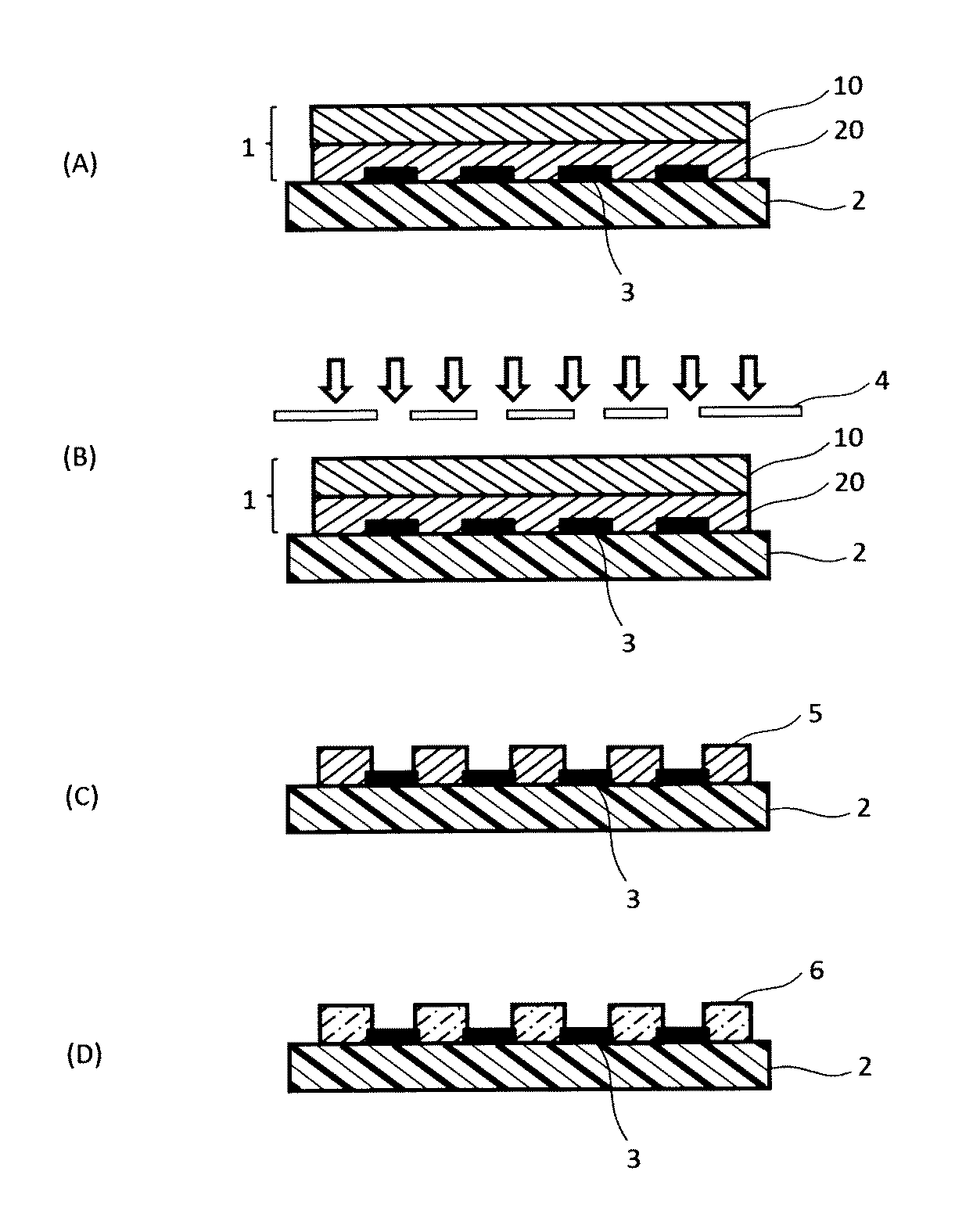
特に、上記式中、X、Yが、それぞれ、メチル基またはエチル基であり、Zがメチルまたはフェニルであり、nが0であり、Arが、フェニレン、ナフチレン、チオフェンまたはチエニレンであるオキシムエステル系光重合開始剤が好ましい。 In particular, the oxime ester system in which X and Y are each a methyl group or an ethyl group, Z is methyl or phenyl, n is 0, and Ar is phenylene, naphthylene, thiophene or thienylene in the above formula Photoinitiators are preferred.
好ましいカルバゾールオキシムエステル化合物として、下記一般式で表すことができる化合物を挙げることもできる。
R2は、炭素原子数1〜4のアルキル基、炭素原子数1〜4のアルコキシ基、または、炭素原子数1〜4のアルキル基もしくはアルコキシ基で置換されていてもよいフェニル基を表す。
R3は、酸素原子または硫黄原子で連結されていてもよく、フェニル基で置換されていてもよい炭素原子数1〜20のアルキル基、炭素原子数1〜4のアルコキシ基で置換されていてもよいベンジル基を表す。
R4は、ニトロ基、または、X−C(=O)−で表されるアシル基を表す。
Xは、炭素原子数1〜4のアルキル基で置換されていてもよいアリール基、チエニル基、モルホリノ基、チオフェニル基、または、下記式で示される構造を表す。)
Preferred examples of the carbazole oxime ester compound include compounds that can be represented by the following general formula.
R 2 represents an alkyl group having 1 to 4 carbon atoms, an alkoxy group having 1 to 4 carbon atoms, or a phenyl group which may be substituted with an alkyl group having 1 to 4 carbon atoms or an alkoxy group.
R 3 may be linked with an oxygen atom or a sulfur atom, and may be substituted with an alkyl group having 1 to 20 carbon atoms and an alkoxy group having 1 to 4 carbon atoms which may be substituted with a phenyl group. Represents a good benzyl group.
R 4 represents a nitro group or an acyl group represented by X—C (═O) —.
X represents an aryl group, a thienyl group, a morpholino group, a thiophenyl group, or a structure represented by the following formula, which may be substituted with an alkyl group having 1 to 4 carbon atoms. )
その他、特開2004−359639号公報、特開2005−097141号公報、特開2005−220097号公報、特開2006−160634号公報、特開2008−094770号公報、特表2008−509967号公報、特表2009−040762号公報、特開2011−80036号公報記載のカルバゾールオキシムエステル化合物等を挙げることができる。 In addition, JP-A-2004-359639, JP-A-2005-097141, JP-A-2005-220097, JP-A-2006-160634, JP-A-2008-094770, JP-A-2008-509967, Specific examples include carbazole oxime ester compounds described in JP2009-040762A and JP2011-80036A.
オキシムエステル系光重合開始剤を使用する場合の配合量は、カルボキシル基含有感光性樹脂100質量部に対して、0.01〜5質量部とすることが好ましい。0.01質量部以上とすることにより、銅上での光硬化性がより確実となり、耐薬品性などの塗膜特性が向上する。また、5質量部以下とすることにより、塗膜表面での光吸収が抑えられ、深部の硬化性も向上する傾向がある。より好ましくは、カルボキシル基含有感光性樹脂100質量部に対して0.5〜3質量部である。 The amount of the oxime ester photopolymerization initiator used is preferably 0.01 to 5 parts by mass with respect to 100 parts by mass of the carboxyl group-containing photosensitive resin. By setting it as 0.01 mass part or more, photocurability on copper becomes more reliable and coating-film characteristics, such as chemical resistance, improve. Moreover, the light absorption in the coating-film surface is suppressed by setting it as 5 mass parts or less, and there exists a tendency for the sclerosis | hardenability of a deep part to improve. More preferably, it is 0.5-3 mass parts with respect to 100 mass parts of carboxyl group-containing photosensitive resin.
α−アミノアセトフェノン系光重合開始剤としては、具体的には、2−メチル−1−[4−(メチルチオ)フェニル]−2−モルホリノプロパノン−1、2−ベンジル−2−ジメチルアミノ−1−(4−モルホリノフェニル)−ブタン−1−オン、2−(ジメチルアミノ)−2−[(4−メチルフェニル)メチル]−1−[4−(4−モルホリニル)フェニル]−1−ブタノン、N,N−ジメチルアミノアセトフェノンなどが挙げられる。市販品としては、BASFジャパン社製のイルガキュア907、イルガキュア369、イルガキュア379などが挙げられる。 As the α-aminoacetophenone photopolymerization initiator, specifically, 2-methyl-1- [4- (methylthio) phenyl] -2-morpholinopropanone-1, 2-benzyl-2-dimethylamino-1 -(4-morpholinophenyl) -butan-1-one, 2- (dimethylamino) -2-[(4-methylphenyl) methyl] -1- [4- (4-morpholinyl) phenyl] -1-butanone, N, N-dimethylaminoacetophenone and the like can be mentioned. Examples of commercially available products include Irgacure 907, Irgacure 369, and Irgacure 379 manufactured by BASF Japan.
アシルホスフィンオキサイド系光重合開始剤としては、具体的には2,4,6−トリメチルベンゾイルジフェニルホスフィンオキサイド、ビス(2,4,6−トリメチルベンゾイル)−フェニルホスフィンオキサイド、ビス(2,6−ジメトキシベンゾイル)−2,4,4−トリメチル−ペンチルホスフィンオキサイドなどが挙げられる。市販品としては、BASFジャパン社製のルシリン(登録商標)TPO、イルガキュア819などが挙げられる。 Specific examples of the acylphosphine oxide photopolymerization initiator include 2,4,6-trimethylbenzoyldiphenylphosphine oxide, bis (2,4,6-trimethylbenzoyl) -phenylphosphine oxide, and bis (2,6-dimethoxy). And benzoyl) -2,4,4-trimethyl-pentylphosphine oxide. Examples of commercially available products include Lucillin (registered trademark) TPO, Irgacure 819 manufactured by BASF Japan.
α−アミノアセトフェノン系光重合開始剤またはアシルホスフィンオキサイド系光重合開始剤を用いる場合のそれぞれの配合量は、カルボキシル基含有感光性樹脂100質量部に対して、0.01〜15質量部であることが好ましい。0.01質量部以上とすることにより、銅上での光硬化性がより確実となり、耐薬品性などの塗膜特性が向上する。また、15質量部以下とすることにより、十分なアウトガスの低減効果が得られ、さらに硬化被膜表面での光吸収が抑えられ、深部の硬化性も向上する。より好ましくはカルボキシル基含有感光性樹脂100質量部に対して0.5〜10質量部である。 Each compounding amount in the case of using an α-aminoacetophenone photopolymerization initiator or an acylphosphine oxide photopolymerization initiator is 0.01 to 15 parts by mass with respect to 100 parts by mass of the carboxyl group-containing photosensitive resin. It is preferable. By setting it as 0.01 mass part or more, photocurability on copper becomes more reliable and coating-film characteristics, such as chemical resistance, improve. Moreover, by setting it as 15 mass parts or less, sufficient reduction effect of an outgas is acquired, Furthermore, the light absorption in the cured film surface is suppressed, and the sclerosis | hardenability of a deep part improves. More preferably, it is 0.5-10 mass parts with respect to 100 mass parts of carboxyl group-containing photosensitive resin.
また、光重合開始剤としてはBASFジャパン社製のイルガキュア389、イルガキュア784も好適に用いることができる。 Further, as a photopolymerization initiator, Irgacure 389 and Irgacure 784 manufactured by BASF Japan can also be suitably used.
上記した光重合開始剤と併用して、光開始助剤または増感剤を用いてもよい。光開始助剤または増感剤としては、ベンゾイン化合物、アセトフェノン化合物、アントラキノン化合物、チオキサントン化合物、ケタール化合物、ベンゾフェノン化合物、3級アミン化合物、およびキサントン化合物などを挙げることができる。これらの化合物は、光重合開始剤として用いることができる場合もあるが、光重合開始剤と併用して用いることが好ましい。また、光開始助剤または増感剤は1種類を単独で用いてもよく、2種以上を併用してもよい。 A photoinitiator or sensitizer may be used in combination with the above-described photopolymerization initiator. Examples of the photoinitiation assistant or sensitizer include benzoin compounds, acetophenone compounds, anthraquinone compounds, thioxanthone compounds, ketal compounds, benzophenone compounds, tertiary amine compounds, and xanthone compounds. These compounds may be used as a photopolymerization initiator in some cases, but are preferably used in combination with a photopolymerization initiator. Moreover, a photoinitiator auxiliary or a sensitizer may be used individually by 1 type, and may use 2 or more types together.
ベンゾイン化合物としては、例えばベンゾイン、ベンゾインメチルエーテル、ベンゾインエチルエーテル、ベンゾインイソプロピルエーテルなどが挙げられる。また、アセトフェノン化合物としては、例えばアセトフェノン、2,2−ジメトキシ−2−フェニルアセトフェノン、2,2−ジエトキシ−2−フェニルアセトフェノン、1,1−ジクロロアセトフェノンなどが挙げられる。また、アントラキノン化合物としては、例えば2−メチルアントラキノン、2−エチルアントラキノン、2−t−ブチルアントラキノン、1−クロロアントラキノンなどが挙げられる。また、チオキサントン化合物としては、例えば2,4−ジメチルチオキサントン、2,4−ジエチルチオキサントン、2−クロロチオキサントン、2,4−ジイソプロピルチオキサントンなどが挙げられる。また、 ケタール化合物としては、例えばアセトフェノンジメチルケタール、ベンジルジメチルケタールなどが挙げられる。さらに、ベンゾフェノン化合物としては、例えばベンゾフェノン、4−ベンゾイルジフェニルスルフィド、4−ベンゾイル−4’−メチルジフェニルスルフィド、4−ベンゾイル−4’−エチルジフェニルスルフィド、4−ベンゾイル−4’−プロピルジフェニルスルフィドなどが挙げられる。 Examples of the benzoin compound include benzoin, benzoin methyl ether, benzoin ethyl ether, and benzoin isopropyl ether. Examples of the acetophenone compound include acetophenone, 2,2-dimethoxy-2-phenylacetophenone, 2,2-diethoxy-2-phenylacetophenone, 1,1-dichloroacetophenone, and the like. Examples of the anthraquinone compound include 2-methylanthraquinone, 2-ethylanthraquinone, 2-t-butylanthraquinone, 1-chloroanthraquinone, and the like. Examples of the thioxanthone compound include 2,4-dimethylthioxanthone, 2,4-diethylthioxanthone, 2-chlorothioxanthone, and 2,4-diisopropylthioxanthone. Examples of the ketal compound include acetophenone dimethyl ketal and benzyl dimethyl ketal. Furthermore, examples of the benzophenone compound include benzophenone, 4-benzoyl diphenyl sulfide, 4-benzoyl-4′-methyl diphenyl sulfide, 4-benzoyl-4′-ethyl diphenyl sulfide, 4-benzoyl-4′-propyl diphenyl sulfide, and the like. Can be mentioned.
3級アミン化合物としては、例えばエタノールアミン化合物、ジアルキルアミノベンゼン構造を有する化合物、例えば、市販品では、4,4’−ジメチルアミノベンゾフェノン(日本曹達社製ニッソキュアー(登録商標)MABP)、4,4’−ジエチルアミノベンゾフェノン(保土ヶ谷化学社製EAB)などのジアルキルアミノベンゾフェノン、7−(ジエチルアミノ)−4−メチル−2H−1−ベンゾピラン−2−オン(7−(ジエチルアミノ)−4−メチルクマリン)などのジアルキルアミノ基含有クマリン化合物、4−ジメチルアミノ安息香酸エチル(日本化薬社製カヤキュアー(登録商標)EPA)、2−ジメチルアミノ安息香酸エチル(インターナショナルバイオ−シンセティクス社製Quantacure DMB)、4−ジメチルアミノ安息香酸(n−ブトキシ)エチル(インターナショナルバイオ−シンセエティックス社製Quantacure BEA)、p−ジメチルアミノ安息香酸イソアミルエチルエステル(日本化薬社製カヤキュアーDMBI)、4−ジメチルアミノ安息香酸2−エチルヘキシル(Van Dyk社製Esolol 507)などが挙げられる。3級アミン化合物としては、ジアルキルアミノベンゼン構造を有する化合物が好ましく、中でも、ジアルキルアミノベンゾフェノン化合物、最大吸収波長が350〜450nmにあるジアルキルアミノ基含有クマリン化合物およびケトクマリン類が特に好ましい。 Examples of the tertiary amine compound include an ethanolamine compound and a compound having a dialkylaminobenzene structure, such as 4,4′-dimethylaminobenzophenone (Nissoure (registered trademark) MABP manufactured by Nippon Soda Co., Ltd.), 4,4 Dialkylaminobenzophenone such as' -diethylaminobenzophenone (EAB manufactured by Hodogaya Chemical Co., Ltd.), 7- (diethylamino) -4-methyl-2H-1-benzopyran-2-one (7- (diethylamino) -4-methylcoumarin), etc. Dialkylamino group-containing coumarin compound, ethyl 4-dimethylaminobenzoate (Kayacure (registered trademark) EPA manufactured by Nippon Kayaku Co., Ltd.), ethyl 2-dimethylaminobenzoate (Quantacure DMB manufactured by International Bio-Synthetics), 4-di Tylaminobenzoic acid (n-butoxy) ethyl (Quantacure BEA manufactured by International Bio-Synthetics), p-dimethylaminobenzoic acid isoamylethyl ester (Nippon Kayaku Co., Ltd. Kayacure DMBI), 4-dimethylaminobenzoic acid 2-ethylhexyl (Esolol 507 manufactured by Van Dyk). As the tertiary amine compound, a compound having a dialkylaminobenzene structure is preferable, and among them, a dialkylaminobenzophenone compound, a dialkylamino group-containing coumarin compound having a maximum absorption wavelength of 350 to 450 nm, and ketocoumarins are particularly preferable.
ジアルキルアミノベンゾフェノン化合物としては、4,4’−ジエチルアミノベンゾフェノンが毒性が低いことから好ましい。ジアルキルアミノ基含有クマリン化合物は、最大吸収波長が350〜410nmと紫外線領域にあるため、着色が少なく、無色透明な感光性組成物はもとより、着色顔料を用い、着色顔料自体の色を反映した着色ソルダーレジスト膜を得ることが可能となる。特に、7−(ジエチルアミノ)−4−メチル−2H−1−ベンゾピラン−2−オンが、波長400〜410nmのレーザー光に対して優れた増感効果を示すことから好ましい。 As the dialkylaminobenzophenone compound, 4,4′-diethylaminobenzophenone is preferable because of its low toxicity. Dialkylamino group-containing coumarin compounds have a maximum absorption wavelength in the ultraviolet region of 350 to 410 nm, so they are less colored, and use colored pigments as well as colorless and transparent photosensitive compositions, and colors that reflect the color of the colored pigments themselves It becomes possible to obtain a solder resist film. In particular, 7- (diethylamino) -4-methyl-2H-1-benzopyran-2-one is preferable because it exhibits an excellent sensitizing effect on laser light having a wavelength of 400 to 410 nm.
これらのうち、チオキサントン化合物および3級アミン化合物が好ましい。特に、チオキサントン化合物が含まれることにより、深部硬化性を向上させることができる。 Of these, thioxanthone compounds and tertiary amine compounds are preferred. In particular, by including a thioxanthone compound, it is possible to improve deep curability.
光重合開始剤、光開始助剤、および増感剤の総量は、カルボキシル基含有感光性樹脂100質量部に対して35質量部以下であることが好ましい。35質量部以下とすることにより、これらの光吸収が抑えられ、深部の硬化性も向上する。 The total amount of the photopolymerization initiator, photoinitiator assistant, and sensitizer is preferably 35 parts by mass or less with respect to 100 parts by mass of the carboxyl group-containing photosensitive resin. By setting it as 35 mass parts or less, these light absorption is suppressed and the sclerosis | hardenability of a deep part is also improved.
なお、これら光重合開始剤、光開始助剤、および増感剤は、特定の波長を吸収するため、場合によっては感度が低くなり、紫外線吸収剤として機能することがある。しかしながら、これらは組成物の感度を向上させることだけの目的に用いられるものではない。必要に応じて特定の波長の光を吸収させて、表面の光反応性を高め、レジストのライン形状および開口を垂直、テーパー状、逆テーパー状に変化させるとともに、ライン幅や開口径の加工精度を向上させることができる。 In addition, since these photopolymerization initiators, photoinitiator assistants, and sensitizers absorb a specific wavelength, in some cases, the sensitivity is lowered, and they may function as ultraviolet absorbers. However, they are not used only for the purpose of improving the sensitivity of the composition. Absorbs light of a specific wavelength as necessary to enhance the photoreactivity of the surface, and changes the resist line shape and opening to vertical, tapered, and inversely tapered, and processing accuracy of line width and opening diameter Can be improved.
感光性樹脂層に使用される樹脂組成物には、耐熱性、絶縁信頼性等の特性を向上させる目的で熱硬化性成分が含まれていてもよい。熱硬化性成分としては、イソシアネート化合物、ブロックイソシアネート化合物、アミノ樹脂、マレイミド化合物、ベンゾオキサジン樹脂、カルボジイミド樹脂、シクロカーボネート化合物、多官能エポキシ化合物、多官能オキセタン化合物、エピスルフィド樹脂などの公知慣用の熱硬化性樹脂が使用できる。これらの中でも好ましい熱硬化性成分は、1分子中に複数の環状エーテル基および/または環状チオエーテル基(以下、環状(チオ)エーテル基と略称する)を有する熱硬化性成分である。これら環状(チオ)エーテル基を有する熱硬化性成分は、市販されている種類が多く、その構造によって多様な特性を付与することができる。 The resin composition used for the photosensitive resin layer may contain a thermosetting component for the purpose of improving characteristics such as heat resistance and insulation reliability. Known thermosetting components such as isocyanate compounds, blocked isocyanate compounds, amino resins, maleimide compounds, benzoxazine resins, carbodiimide resins, cyclocarbonate compounds, polyfunctional epoxy compounds, polyfunctional oxetane compounds, episulfide resins, etc. Resin can be used. Among these, a preferable thermosetting component is a thermosetting component having a plurality of cyclic ether groups and / or cyclic thioether groups (hereinafter abbreviated as cyclic (thio) ether groups) in one molecule. There are many commercially available thermosetting components having a cyclic (thio) ether group, and various properties can be imparted depending on the structure.
分子中に複数の環状(チオ)エーテル基を有する熱硬化性成分は、分子中に3、4または5員環の環状エーテル基、または環状チオエーテル基のいずれか一方または2種類の基を複数有する化合物であり、例えば、分子中に複数のエポキシ基を有する化合物、すなわち多官能エポキシ化合物、分子中に複数のオキセタニル基を有する化合物、すなわち多官能オキセタン化合物、分子中に複数のチオエーテル基を有する化合物、すなわちエピスルフィド樹脂などが挙げられる。 The thermosetting component having a plurality of cyclic (thio) ether groups in the molecule has either one of the three, four or five-membered cyclic ether groups, or the cyclic thioether group, or a plurality of two types of groups in the molecule. Compound, for example, a compound having a plurality of epoxy groups in the molecule, that is, a polyfunctional epoxy compound, a compound having a plurality of oxetanyl groups in the molecule, that is, a polyfunctional oxetane compound, a compound having a plurality of thioether groups in the molecule That is, an episulfide resin etc. are mentioned.
多官能エポキシ化合物としては、例えば、三菱化学社製のjER828、jER834、jER1001、jER1004、DIC社製のエピクロン840、エピクロン850、エピクロン1050、エピクロン2055、東都化成社製のエポトートYD−011、YD−013、YD−127、YD−128、ダウケミカル社製のD.E.R.317、D.E.R.331、D.E.R.661、D.E.R.664、住友化学工業社製のスミ−エポキシESA−011、ESA−014、ELA−115、ELA−128、旭化成工業社製のA.E.R.330、A.E.R.331、A.E.R.661、A.E.R.664等(何れも商品名)のビスフェノールA型エポキシ樹脂;三菱化学社製のjERYL903、DIC社製のエピクロン152、エピクロン165、東都化成社製のエポトートYDB−400、YDB−500、ダウケミカル社製のD.E.R.542、住友化学工業社製のスミ−エポキシESB−400、ESB−700、旭化成工業社製のA.E.R.711、A.E.R.714等(何れも商品名)のブロム化エポキシ樹脂;三菱化学社製のjER152、jER154、ダウケミカル社製のD.E.N.431、D.E.N.438、DIC社製のエピクロンN−730、エピクロンN−770、エピクロンN−865、東都化成社製のエポトートYDCN−701、YDCN−704、日本化薬社製のEPPN−201、EOCN−1025、EOCN−1020、EOCN−104S、RE−306、NC−3000H、住友化学工業社製のスミ−エポキシESCN−195X、ESCN−220、旭化成工業社製のA.E.R.ECN−235、ECN−299等(何れも商品名)のノボラック型エポキシ樹脂;DIC社製のエピクロン830、三菱化学社製jER807、東都化成社製のエポトートYDF−170、YDF−175、YDF−2004等(何れも商品名)のビスフェノールF型エポキシ樹脂;東都化成社製のエポトートST−2004、ST−2007、ST−3000(商品名)等の水添ビスフェノールA型エポキシ樹脂;三菱化学社製のjER604、東都化成社製のエポトートYH−434、住友化学工業社製のスミ−エポキシELM−120等(何れも商品名)のグリシジルアミン型エポキシ樹脂;ダイセル化学工業社製のセロキサイド2021等(商品名)の脂環式エポキシ樹脂;三菱化学社製のYL−933、ダウケミカル社製のT.E.N.、EPPN−501、EPPN−502等(何れも商品名)のトリヒドロキシフェニルメタン型エポキシ樹脂;三菱化学社製のYL−6056、YX−4000、YL−6121(何れも商品名)等のビキシレノール型もしくはビフェノール型エポキシ樹脂またはそれらの混合物;日本化薬社製EBPS−200、旭電化工業社製EPX−30、DIC社製のEXA−1514(商品名)等のビスフェノールS型エポキシ樹脂;三菱化学社製のjER157S(商品名)等のビスフェノールAノボラック型エポキシ樹脂;三菱化学社製のjERYL−931等(商品名)のテトラフェニロールエタン型エポキシ樹脂;日産化学工業社製のTEPIC等(商品名)の複素環式エポキシ樹脂;日本油脂社製ブレンマーDGT等のジグリシジルフタレート樹脂;東都化成社製ZX−1063等のテトラグリシジルキシレノイルエタン樹脂;新日鐵化学社製ESN−190、ESN−360、DIC社製HP−4032、EXA−4750、EXA−4700等のナフタレン基含有エポキシ樹脂;DIC社製HP−7200、HP−7200H等のジシクロペンタジエン骨格を有するエポキシ樹脂、EXA−4816、EXA−4822、EXA−4850シリーズの柔軟強靭エポキシ樹脂;日本油脂社製CP−50S、CP−50M等のグリシジルメタアクリレート共重合系エポキシ樹脂;さらにシクロヘキシルマレイミドとグリシジルメタアクリレートの共重合エポキシ樹脂等が挙げられるが、これらに限られるものではない。これらのエポキシ樹脂は、単独でまたは2種以上を組み合わせて用いることができる。 Examples of the polyfunctional epoxy compound include jER828, jER834, jER1001, and jER1004 manufactured by Mitsubishi Chemical Corporation, Epicron 840 manufactured by DIC, Epicron 850, Epicron 1050, Epicron 2055, Epoto YD-011, YD- manufactured by Tohto Kasei Co., Ltd. 013, YD-127, YD-128, D.C. E. R. 317, D.E. E. R. 331, D.D. E. R. 661, D.D. E. R. 664, Sumitomo Epoxy ESA-011, ESA-014, ELA-115, ELA-128, manufactured by Sumitomo Chemical Co., Ltd., A.A. E. R. 330, A.I. E. R. 331, A.I. E. R. 661, A.I. E. R. Bisphenol A type epoxy resin such as 664 (all trade names); jERYL903 manufactured by Mitsubishi Chemical, Epicron 152, Epicron 165 manufactured by DIC, Epototo YDB-400, YDB-500 manufactured by Tohto Kasei Co., Ltd., manufactured by Dow Chemical Of D. E. R. 542, Sumitomo Epoxy ESB-400, ESB-700 manufactured by Sumitomo Chemical Co., Ltd., A.A. E. R. 711, A.I. E. R. Brominated epoxy resins such as 714 (both trade names); jER152 and jER154 manufactured by Mitsubishi Chemical Corporation, and D.C. E. N. 431, D.D. E. N. 438, Epicron N-730, Epicron N-770, Epicron N-865 manufactured by DIC, Epototo YDCN-701, YDCN-704 manufactured by Tohto Kasei Co., Ltd., EPPN-201, EOCN-1025, EOCN manufactured by Nippon Kayaku Co., Ltd. -1020, EOCN-104S, RE-306, NC-3000H, Sumitomo Epoxy ESCN-195X, ESCN-220, manufactured by Sumitomo Chemical Co., Ltd., A.C. E. R. Novolak type epoxy resins such as ECN-235, ECN-299, etc. (both trade names); Epicron 830 manufactured by DIC, jER807 manufactured by Mitsubishi Chemical Co., Ltd. Epototo YDF-170, YDF-175, YDF-2004 manufactured by Tohto Kasei Co., Ltd. (All trade names) bisphenol F-type epoxy resin; hydrogenated bisphenol A-type epoxy resins such as Epototo ST-2004, ST-2007, ST-3000 (trade name) manufactured by Toto Kasei Co., Ltd .; glycidylamine type epoxy resin such as jER604, Etototo YH-434 manufactured by Tohto Kasei Co., Ltd., Sumi-epoxy ELM-120 manufactured by Sumitomo Chemical Co., Ltd. (both trade names); Celoxide 2021 manufactured by Daicel Chemical Industries Co., Ltd. ) Cycloaliphatic epoxy resin; YL-933 manufactured by Mitsubishi Chemical Corporation, T.W. manufactured by Dow Chemical Co., Ltd. E. N. , EPPN-501, EPPN-502, etc. (all trade names) trihydroxyphenylmethane type epoxy resin; Mitsubishi Chemical Corporation YL-6056, YX-4000, YL-6121 (all trade names) Type or biphenol type epoxy resin or a mixture thereof; bisphenol S type epoxy resin such as EBPS-200 manufactured by Nippon Kayaku Co., Ltd., EPX-30 manufactured by Asahi Denka Kogyo Co., Ltd., EXA-1514 manufactured by DIC Co., Ltd .; Bisphenol A novolac type epoxy resin such as jER157S (trade name) manufactured by Mitsubishi Chemical Corporation; tetraphenylolethane type epoxy resin such as jERYL-931 (trade name) manufactured by Mitsubishi Chemical Corporation; TEPIC manufactured by Nissan Chemical Industries Co., Ltd. (trade name) ) Heterocyclic epoxy resin; diglycidyl phthalate such as Bremer DGT manufactured by NOF Corporation Tetraglycidylxylenoylethane resin such as ZX-1063 manufactured by Tohto Kasei Co., Ltd .; ESN-190, ESN-360 manufactured by Nippon Steel Chemical Co., Ltd., HP-4032, EXA-4750, EXA-4700 manufactured by DIC Naphthalene group-containing epoxy resin; epoxy resin having dicyclopentadiene skeleton such as HP-7200, HP-7200H, etc. manufactured by DIC, EXA-4816, EXA-4822, EXA-4850 series flexible tough epoxy resin; Examples include, but are not limited to, glycidyl methacrylate copolymer epoxy resins such as CP-50S and CP-50M; and a copolymer epoxy resin of cyclohexylmaleimide and glycidyl methacrylate. These epoxy resins can be used alone or in combination of two or more.
多官能オキセタン化合物としては、ビス[(3−メチル−3−オキセタニルメトキシ)メチル]エーテル、ビス[(3−エチル−3−オキセタニルメトキシ)メチル]エーテル、1,4−ビス[(3−メチル−3−オキセタニルメトキシ)メチル]ベンゼン、1,4−ビス[(3−エチル−3−オキセタニルメトキシ)メチル]ベンゼン、(3−メチル−3−オキセタニル)メチルアクリレート、(3−エチル−3−オキセタニル)メチルアクリレート、(3−メチル−3−オキセタニル)メチルメタクリレート、(3−エチル−3−オキセタニル)メチルメタクリレートやそれらのオリゴマーまたは共重合体等の多官能オキセタン類の他、オキセタンアルコールとノボラック樹脂、ポリ(p−ヒドロキシスチレン)、カルド型ビスフェノール類、カリックスアレーン類、カリックスレゾルシンアレーン類、またはシルセスキオキサンなどの水酸基を有する樹脂とのエーテル化物などが挙げられる。その他、オキセタン環を有する不飽和モノマーとアルキル(メタ)アクリレートとの共重合体なども挙げられる。 Polyfunctional oxetane compounds include bis [(3-methyl-3-oxetanylmethoxy) methyl] ether, bis [(3-ethyl-3-oxetanylmethoxy) methyl] ether, 1,4-bis [(3-methyl- 3-Oxetanylmethoxy) methyl] benzene, 1,4-bis [(3-ethyl-3-oxetanylmethoxy) methyl] benzene, (3-methyl-3-oxetanyl) methyl acrylate, (3-ethyl-3-oxetanyl) In addition to polyfunctional oxetanes such as methyl acrylate, (3-methyl-3-oxetanyl) methyl methacrylate, (3-ethyl-3-oxetanyl) methyl methacrylate and oligomers or copolymers thereof, oxetane alcohol and novolak resin, poly (P-hydroxystyrene), cardo-type bisphenol S, calixarenes, calix resorcin arenes, or the like ethers of a resin having a hydroxyl group such as silsesquioxane and the like. In addition, a copolymer of an unsaturated monomer having an oxetane ring and an alkyl (meth) acrylate is also included.
分子中に複数の環状チオエーテル基を有するエピスルフィド樹脂としては、例えば、三菱化学社製のYL7000(ビスフェノールA型エピスルフィド樹脂)などが挙げられる。また、同様の合成方法を用いて、ノボラック型エポキシ樹脂のエポキシ基の酸素原子を硫黄原子に置き換えたエピスルフィド樹脂なども用いることができる。 Examples of the episulfide resin having a plurality of cyclic thioether groups in the molecule include YL7000 (bisphenol A type episulfide resin) manufactured by Mitsubishi Chemical Corporation. Moreover, episulfide resin etc. which replaced the oxygen atom of the epoxy group of the novolak-type epoxy resin with the sulfur atom using the same synthesis method can be used.
分子中に複数の環状(チオ)エーテル基を有する熱硬化性成分の配合量は、カルボキシル基含有感光性樹脂のカルボキシル基1当量に対して、好ましくは0.3〜2.5当量、より好ましくは、0.5〜2.0当量となる範囲である。分子中に複数の環状(チオ)エーテル基を有する熱硬化性成分の配合量を0.3当量以上とすることにより、硬化被膜にカルボキシル基が残存せず、耐熱性、耐アルカリ性、電気絶縁性などが向上する。また、2.5当量以下とすることにより、低分子量の環状(チオ)エーテル基が乾燥塗膜に残存せず、硬化被膜の強度などが向上する。 The blending amount of the thermosetting component having a plurality of cyclic (thio) ether groups in the molecule is preferably 0.3 to 2.5 equivalents, more preferably 1 equivalent to the carboxyl group of the carboxyl group-containing photosensitive resin. Is in the range of 0.5 to 2.0 equivalents. By making the amount of thermosetting component having a plurality of cyclic (thio) ether groups in the molecule 0.3 equivalent or more, no carboxyl group remains in the cured film, heat resistance, alkali resistance, electrical insulation Etc. improve. Moreover, by setting it as 2.5 equivalent or less, the low molecular weight cyclic (thio) ether group does not remain in the dry coating film, and the strength and the like of the cured coating film are improved.
分子中に複数の環状(チオ)エーテル基を有する熱硬化性成分を使用する場合、熱硬化触媒を含有することが好ましい。そのような熱硬化触媒としては、例えば、イミダゾール、2−メチルイミダゾール、2−エチルイミダゾール、2−エチル−4−メチルイミダゾール、2−フェニルイミダゾール、4−フェニルイミダゾール、1−シアノエチル−2−フェニルイミダゾール、1−(2−シアノエチル)−2−エチル−4−メチルイミダゾール等のイミダゾール誘導体;ジシアンジアミド、ベンジルジメチルアミン、4−(ジメチルアミノ)−N,N−ジメチルベンジルアミン、4−メトキシ−N,N−ジメチルベンジルアミン、4−メチル−N,N−ジメチルベンジルアミン等のアミン化合物、アジピン酸ジヒドラジド、セバシン酸ジヒドラジド等のヒドラジン化合物;トリフェニルホスフィン等のリン化合物などが挙げられる。また、市販されているものとしては、例えば四国化成工業社製の2MZ−A、2MZ−OK、2PHZ、2P4BHZ、2P4MHZ(いずれもイミダゾール系化合物の商品名)、サンアプロ社製のU−CAT(登録商標)3503N、U−CAT3502T(いずれもジメチルアミンのブロックイソシアネート化合物の商品名)、DBU、DBN、U−CATSA102、U−CAT5002(いずれも二環式アミジン化合物およびその塩)などが挙げられる。特に、これらに限られるものではなく、エポキシ樹脂やオキセタン化合物の熱硬化触媒、もしくはエポキシ基および/またはオキセタニル基とカルボキシル基の反応を促進するものであればよく、単独でまたは2種以上を混合して使用してもかまわない。また、グアナミン、アセトグアナミン、ベンゾグアナミン、メラミン、2,4−ジアミノ−6−メタクリロイルオキシエチル−S−トリアジン、2−ビニル−2,4−ジアミノ−S−トリアジン、2−ビニル−4,6−ジアミノ−S−トリアジン・イソシアヌル酸付加物、2,4−ジアミノ−6−メタクリロイルオキシエチル−S−トリアジン・イソシアヌル酸付加物等のS−トリアジン誘導体を用いることもでき、好ましくはこれら密着性付与剤としても機能する化合物を熱硬化触媒と併用する。 When using a thermosetting component having a plurality of cyclic (thio) ether groups in the molecule, it is preferable to contain a thermosetting catalyst. Examples of such thermosetting catalysts include imidazole, 2-methylimidazole, 2-ethylimidazole, 2-ethyl-4-methylimidazole, 2-phenylimidazole, 4-phenylimidazole, 1-cyanoethyl-2-phenylimidazole. Imidazole derivatives such as 1- (2-cyanoethyl) -2-ethyl-4-methylimidazole; dicyandiamide, benzyldimethylamine, 4- (dimethylamino) -N, N-dimethylbenzylamine, 4-methoxy-N, N -Amine compounds such as dimethylbenzylamine and 4-methyl-N, N-dimethylbenzylamine; hydrazine compounds such as adipic acid dihydrazide and sebacic acid dihydrazide; and phosphorus compounds such as triphenylphosphine. Examples of commercially available products include 2MZ-A, 2MZ-OK, 2PHZ, 2P4BHZ, 2P4MHZ (both trade names of imidazole compounds) manufactured by Shikoku Kasei Kogyo Co., Ltd., and U-CAT (registered by San Apro). Trademarks) 3503N, U-CAT3502T (all are trade names of blocked isocyanate compounds of dimethylamine), DBU, DBN, U-CATSA102, U-CAT5002 (all are bicyclic amidine compounds and salts thereof), and the like. In particular, it is not limited to these, as long as it is a thermosetting catalyst for epoxy resins and oxetane compounds, or any catalyst that promotes the reaction of epoxy groups and / or oxetanyl groups with carboxyl groups, either alone or in combination of two or more. Can be used. Also, guanamine, acetoguanamine, benzoguanamine, melamine, 2,4-diamino-6-methacryloyloxyethyl-S-triazine, 2-vinyl-2,4-diamino-S-triazine, 2-vinyl-4,6-diamino S-triazine derivatives such as -S-triazine and isocyanuric acid adducts and 2,4-diamino-6-methacryloyloxyethyl-S-triazine and isocyanuric acid adducts can also be used. A compound that also functions in combination with a thermosetting catalyst.
熱硬化触媒の配合量は、分子中に複数の環状(チオ)エーテル基を有する熱硬化性成分100質量部に対して、好ましくは0.1〜20質量部、より好ましくは0.5〜15.0質量部である。 The blending amount of the thermosetting catalyst is preferably 0.1 to 20 parts by mass, more preferably 0.5 to 15 parts per 100 parts by mass of the thermosetting component having a plurality of cyclic (thio) ether groups in the molecule. 0.0 part by mass.
アミノ樹脂としては、メラミン誘導体、ベンゾグアナミン誘導体などのアミノ樹脂が挙げられる。例えばメチロールメラミン化合物、メチロールベンゾグアナミン化合物、メチロールグリコールウリル化合物およびメチロール尿素化合物などがある。さらに、アルコキシメチル化メラミン化合物、アルコキシメチル化ベンゾグアナミン化合物、アルコキシメチル化グリコールウリル化合物およびアルコキシメチル化尿素化合物は、それぞれのメチロールメラミン化合物、メチロールベンゾグアナミン化合物、メチロールグリコールウリル化合物およびメチロール尿素化合物のメチロール基をアルコキシメチル基に変換することにより得られる。このアルコキシメチル基の種類については特に限定されるものではなく、例えばメトキシメチル基、エトキシメチル基、プロポキシメチル基、ブトキシメチル基等とすることができる。特に人体や環境に優しいホルマリン濃度が0.2%以下のメラミン誘導体が好ましい。 Amino resins include amino resins such as melamine derivatives and benzoguanamine derivatives. Examples include methylol melamine compounds, methylol benzoguanamine compounds, methylol glycoluril compounds, and methylol urea compounds. Furthermore, the alkoxymethylated melamine compound, alkoxymethylated benzoguanamine compound, alkoxymethylated glycoluril compound and alkoxymethylated urea compound have the methylol group of the respective methylolmelamine compound, methylolbenzoguanamine compound, methylolglycoluril compound and methylolurea compound. Obtained by conversion to an alkoxymethyl group. The type of the alkoxymethyl group is not particularly limited and can be, for example, a methoxymethyl group, an ethoxymethyl group, a propoxymethyl group, a butoxymethyl group, or the like. In particular, a melamine derivative having a formalin concentration which is friendly to the human body and the environment is preferably 0.2% or less.
アミノ樹脂の市販品としては、例えばサイメル300、同301、同303、同370、同325、同327、同701、同266、同267、同238、同1141、同272、同202、同1156、同1158、同1123、同1170、同1174、同UFR65、同300(以上、三井サイアナミッド社製)、ニカラックMx−750、同Mx−032、同Mx−270、同Mx−280、同Mx−290、同Mx−706、同Mx−708、同Mx−40、同Mx−31、同Ms−11、同Mw−30、同Mw−30HM、同Mw−390、同Mw−100LM、同Mw−750LM、(以上、三和ケミカル社製)等を挙げることができる。 Examples of commercially available amino resins include Cymel 300, 301, 303, 370, 325, 327, 701, 266, 267, 238, 1141, 272, 202, 1156. 1158, 1123, 1170, 1174, UFR65, 300 (above, manufactured by Mitsui Cyanamid Co., Ltd.), Nicarak Mx-750, Mx-032, Mx-270, Mx-280, Mx- 290, Mx-706, Mx-708, Mx-40, Mx-31, Ms-11, Mw-30, Mw-30HM, Mw-390, Mw-100LM, Mw- 750LM (made by Sanwa Chemical Co., Ltd.) and the like.
イソシアネート化合物としては、分子中に複数のイソシアネート基を有するポリイソシアネート化合物を用いることができる。ポリイソシアネート化合物としては、例えば、芳香族ポリイソシアネート、脂肪族ポリイソシアネートまたは脂環式ポリイソシアネートが用いられる。芳香族ポリイソシアネートの具体例としては、4,4’−ジフェニルメタンジイソシアネート、2,4−トリレンジイソシアネート、2,6−トリレンジイソシアネート、ナフタレン−1,5−ジイソシアネート、o−キシリレンジイソシアネート、m−キシリレンジイソシアネートおよび2,4−トリレンダイマーが挙げられる。脂肪族ポリイソシアネートの具体例としては、テトラメチレンジイソシアネート、ヘキサメチレンジイソシアネート、メチレンジイソシアネート、トリメチルヘキサメチレンジイソシアネート、4,4−メチレンビス(シクロヘキシルイソシアネート)およびイソホロンジイソシアネートが挙げられる。脂環式ポリイソシアネートの具体例としてはビシクロヘプタントリイソシアネートが挙げられる。並びに先に挙げられたイソシアネート化合物のアダクト体、ビューレット体およびイソシアヌレート体が挙げられる。 As the isocyanate compound, a polyisocyanate compound having a plurality of isocyanate groups in the molecule can be used. As the polyisocyanate compound, for example, aromatic polyisocyanate, aliphatic polyisocyanate or alicyclic polyisocyanate is used. Specific examples of the aromatic polyisocyanate include 4,4′-diphenylmethane diisocyanate, 2,4-tolylene diisocyanate, 2,6-tolylene diisocyanate, naphthalene-1,5-diisocyanate, o-xylylene diisocyanate, m- Examples include xylylene diisocyanate and 2,4-tolylene dimer. Specific examples of the aliphatic polyisocyanate include tetramethylene diisocyanate, hexamethylene diisocyanate, methylene diisocyanate, trimethylhexamethylene diisocyanate, 4,4-methylenebis (cyclohexyl isocyanate), and isophorone diisocyanate. Specific examples of the alicyclic polyisocyanate include bicycloheptane triisocyanate. In addition, adduct bodies, burette bodies and isocyanurate bodies of the isocyanate compounds mentioned above may be mentioned.
ブロックイソシアネート化合物に含まれるブロック化イソシアネート基は、イソシアネート基がブロック剤との反応により保護されて一時的に不活性化された基である。所定温度に加熱されたときにそのブロック剤が解離してイソシアネート基が生成する。 The blocked isocyanate group contained in the blocked isocyanate compound is a group in which the isocyanate group is protected by reaction with a blocking agent and temporarily deactivated. When heated to a predetermined temperature, the blocking agent is dissociated to produce isocyanate groups.
ブロックイソシアネート化合物としては、イソシアネート化合物とイソシアネートブロック剤との付加反応生成物が用いられる。ブロック剤と反応し得るイソシアネート化合物としては、イソシアヌレート型、ビウレット型、アダクト型等が挙げられる。ブロックイソシアネート化合物を合成する為に用いられるイソシアネート化合物としては、例えば、芳香族ポリイソシアネート、脂肪族ポリイソシアネートまたは脂環式ポリイソシアネートが挙げられる。芳香族ポリイソシアネート、脂肪族ポリイソシアネート、脂環式ポリイソシアネートの具体例としては、先に例示したような化合物が挙げられる。 As the blocked isocyanate compound, an addition reaction product of an isocyanate compound and an isocyanate blocking agent is used. Examples of the isocyanate compound that can react with the blocking agent include isocyanurate type, biuret type, and adduct type. As an isocyanate compound used in order to synthesize | combine a block isocyanate compound, aromatic polyisocyanate, aliphatic polyisocyanate, or alicyclic polyisocyanate is mentioned, for example. Specific examples of the aromatic polyisocyanate, aliphatic polyisocyanate, and alicyclic polyisocyanate include the compounds exemplified above.
イソシアネートブロック剤としては、例えば、フェノール、クレゾール、キシレノール、クロロフェノールおよびエチルフェノール等のフェノール系ブロック剤;ε−カプロラクタム、δ−パレロラクタム、γ−ブチロラクタムおよびβ−プロピオラクタム等のラクタム系ブロック剤;アセト酢酸エチルおよびアセチルアセトンなどの活性メチレン系ブロック剤;メタノール、エタノール、プロパノール、ブタノール、アミルアルコール、エチレングリコールモノメチルエーテル、エチレングリコールモノエチルエーテル、エチレングリコールモノブチルエーテル、ジエチレングリコールモノメチルエーテル、プロピレングリコールモノメチルエーテル、ベンジルエーテル、グリコール酸メチル、グリコール酸ブチル、ジアセトンアルコール、乳酸メチルおよび乳酸エチル等のアルコール系ブロック剤;ホルムアルデヒドキシム、アセトアルドキシム、アセトキシム、メチルエチルケトキシム、ジアセチルモノオキシム、シクロヘキサンオキシム等のオキシム系ブロック剤;ブチルメルカプタン、ヘキシルメルカプタン、t−ブチルメルカプタン、チオフェノール、メチルチオフェノール、エチルチオフェノール等のメルカプタン系ブロック剤;酢酸アミド、ベンズアミド等の酸アミド系ブロック剤;コハク酸イミドおよびマレイン酸イミド等のイミド系ブロック剤;キシリジン、アニリン、ブチルアミン、ジブチルアミン等のアミン系ブロック剤;イミダゾール、2−エチルイミダゾール等のイミダゾール系ブロック剤;メチレンイミンおよびプロピレンイミン等のイミン系ブロック剤等が挙げられる。 Examples of the isocyanate blocking agent include phenolic blocking agents such as phenol, cresol, xylenol, chlorophenol and ethylphenol; lactam blocking agents such as ε-caprolactam, δ-palerolactam, γ-butyrolactam and β-propiolactam; Active methylene blocking agents such as ethyl acetoacetate and acetylacetone; methanol, ethanol, propanol, butanol, amyl alcohol, ethylene glycol monomethyl ether, ethylene glycol monoethyl ether, ethylene glycol monobutyl ether, diethylene glycol monomethyl ether, propylene glycol monomethyl ether, benzyl Ether, methyl glycolate, butyl glycolate, diacetone alcohol, Alcohol blocking agents such as methyl acid and ethyl lactate; oxime blocking agents such as formaldehyde oxime, acetaldoxime, acetoxime, methyl ethyl ketoxime, diacetyl monooxime, cyclohexane oxime; butyl mercaptan, hexyl mercaptan, t-butyl mercaptan, thiophenol Mercaptan blocking agents such as methylthiophenol and ethylthiophenol; acid amide blocking agents such as acetic acid amide and benzamide; imide blocking agents such as succinimide and maleic imide; xylidine, aniline, butylamine, dibutylamine, etc. Amine-based blocking agents; imidazole-based blocking agents such as imidazole and 2-ethylimidazole; imine-based blocks such as methyleneimine and propyleneimine Agents and the like.
ブロックイソシアネート化合物は市販のものであってもよく、例えば、スミジュールBL−3175、BL−4165、BL−1100、BL−1265、デスモジュールTPLS−2957、TPLS−2062、TPLS−2078、TPLS−2117、デスモサーム2170、デスモサーム2265(以上、住友バイエルウレタン社製、商品名)、コロネート2512、コロネート2513、コロネート2520(以上、日本ポリウレタン工業社製、商品名)、B−830、B−815、B−846、B−870、B−874、B−882(以上、三井武田ケミカル社製、商品名)、TPA−B80E、17B−60PX、E402−B80T(以上、旭化成ケミカルズ社製、商品名)等が挙げられる。なお、スミジュールBL−3175、BL−4265はブロック剤としてメチルエチルオキシムを用いて得られるものである。 The block isocyanate compound may be commercially available, for example, Sumidur BL-3175, BL-4165, BL-1100, BL-1265, Desmodur TPLS-2957, TPLS-2062, TPLS-2078, TPLS-2117. , Desmotherm 2170, Desmotherm 2265 (above, Sumitomo Bayer Urethane Co., Ltd., trade name), Coronate 2512, Coronate 2513, Coronate 2520 (above, Nihon Polyurethane Industry Co., Ltd., trade name), B-830, B-815, B- 846, B-870, B-874, B-882 (above, Mitsui Takeda Chemicals, trade name), TPA-B80E, 17B-60PX, E402-B80T (above, Asahi Kasei Chemicals, trade name), etc. Can be mentioned. Sumijoules BL-3175 and BL-4265 are obtained using methyl ethyl oxime as a blocking agent.
感光性樹脂組成物には、水酸基やカルボキシル基とイソシアネート基との硬化反応を促進させるためにウレタン化触媒を添加してもよい。ウレタン化触媒としては、錫系触媒、金属塩化物、金属アセチルアセトネート塩、金属硫酸塩、アミン化合物、およびアミン塩の少なくとも何れか1種から選択されるウレタン化触媒を使用することが好ましい。 A urethanization catalyst may be added to the photosensitive resin composition in order to accelerate the curing reaction between a hydroxyl group or a carboxyl group and an isocyanate group. As the urethanization catalyst, it is preferable to use a urethanization catalyst selected from at least one of tin-based catalysts, metal chlorides, metal acetylacetonate salts, metal sulfates, amine compounds, and amine salts.
錫系触媒としては、例えばスタナスオクトエート、ジブチル錫ジラウレートなどの有機すず化合物、無機すず化合物などが挙げられる。また、金属塩化物としては、Cr、Mn、Co、Ni、Fe、CuおよびAlからなる群から選ばれる金属の塩化物で、例えば、塩化第二コバルト、塩化第一ニッケル、塩化第二鉄などが挙げられる。また、金属アセチルアセトネート塩は、Cr、Mn、Co、Ni、Fe、CuおよびAlからなる群から選ばれる金属のアセチルアセトネート塩であり、例えば、コバルトアセチルアセトネート、ニッケルアセチルアセトネート、鉄アセチルアセトネートなどが挙げられる。さらに、金属硫酸塩としては、Cr、Mn、Co、Ni、Fe、CuおよびAlからなる群から選ばれる金属の硫酸塩で、例えば、硫酸銅などが挙げられる。 Examples of the tin-based catalyst include organic tin compounds such as stannous octoate and dibutyltin dilaurate, and inorganic tin compounds. The metal chloride is a metal chloride selected from the group consisting of Cr, Mn, Co, Ni, Fe, Cu and Al. For example, cobalt chloride, nickel chloride, ferric chloride, etc. Is mentioned. The metal acetylacetonate salt is a metal acetylacetonate salt selected from the group consisting of Cr, Mn, Co, Ni, Fe, Cu and Al. For example, cobalt acetylacetonate, nickel acetylacetonate, iron Examples include acetylacetonate. Furthermore, the metal sulfate is a metal sulfate selected from the group consisting of Cr, Mn, Co, Ni, Fe, Cu, and Al, and examples thereof include copper sulfate.
アミン化合物としては、例えば、従来公知のトリエチレンジアミン、N,N,N’,N’−テトラメチル−1,6−ヘキサンジアミン、ビス(2−ジメチルアミノエチル)エーテル、N,N,N’,N”,N”−ペンタメチルジエチレントリアミン、N−メチルモルフォリン、N−エチルモルフォリン、N,N−ジメチルエタノールアミン、ジモルホリノジエチルエーテル、N−メチルイミダゾール、ジメチルアミノピリジン、トリアジン、N’−(2−ヒドロキシエチル)−N,N,N’−トリメチルービス(2−アミノエチル)エーテル、N,N−ジメチルヘキサノールアミン、N,N−ジメチルアミノエトキシエタノール、N,N,N’−トリメチル−N’−(2−ヒドロキシエチル)エチレンジアミン、N−(2−ヒドロキシエチル)−N,N’,N”,N”−テトラメチルジエチレントリアミン、N−(2−ヒドロキシプロピル)−N,N’,N”,N”−テトラメチルジエチレントリアミン、N,N,N’−トリメチル−N’−(2−ヒドロキシエチル)プロパンジアミン、N−メチル−N’−(2−ヒドロキシエチル)ピペラジン、ビス(N,N−ジメチルアミノプロピル)アミン、ビス(N,N−ジメチルアミノプロピル)イソプロパノールアミン、2−アミノキヌクリジン、3−アミノキヌクリジン、4−アミノキヌクリジン、2−キヌクリジオール、3−キヌクリジノール、4−キヌクリジノール、1−(2’−ヒドロキシプロピル)イミダゾール、1−(2’−ヒドロキシプロピル)−2−メチルイミダゾール、1−(2’−ヒドロキシエチル)イミダゾール、1−(2’−ヒドロキシエチル)−2−メチルイミダゾール、1−(2’−ヒドロキシプロピル)−2−メチルイミダゾール、1−(3’−アミノプロピル)イミダゾール、1−(3’−アミノプロピル)−2−メチルイミダゾール、1−(3’−ヒドロキシプロピル)イミダゾール、1−(3’−ヒドロキシプロピル)−2−メチルイミダゾール、N,N−ジメチルアミノプロピル−N’−(2−ヒドロキシエチル)アミン、N,N−ジメチルアミノプロピル−N’,N’−ビス(2−ヒドロキシエチル)アミン、N,N−ジメチルアミノプロピル−N’,N’−ビス(2−ヒドロキシプロピル)アミン、N,N−ジメチルアミノエチル−N’,N’−ビス(2−ヒドロキシエチル)アミン、N,N−ジメチルアミノエチル−N’,N’−ビス(2−ヒドロキシプロピル)アミン、メラミンまたは/およびベンゾグアナミンなどが挙げられる。 Examples of the amine compound include conventionally known triethylenediamine, N, N, N ′, N′-tetramethyl-1,6-hexanediamine, bis (2-dimethylaminoethyl) ether, N, N, N ′, N ″, N ″ -pentamethyldiethylenetriamine, N-methylmorpholine, N-ethylmorpholine, N, N-dimethylethanolamine, dimorpholinodiethyl ether, N-methylimidazole, dimethylaminopyridine, triazine, N ′-( 2-hydroxyethyl) -N, N, N′-trimethyl-bis (2-aminoethyl) ether, N, N-dimethylhexanolamine, N, N-dimethylaminoethoxyethanol, N, N, N′-trimethyl-N ′ -(2-hydroxyethyl) ethylenediamine, N- (2-hydroxyethyl) -N, N ', N ", N" -tetramethyldiethylenetriamine, N- (2-hydroxypropyl) -N, N', N ", N" -tetramethyldiethylenetriamine, N, N, N'-trimethyl-N '-(2-hydroxyethyl) propanediamine, N-methyl-N'-(2-hydroxyethyl) piperazine, bis (N, N-dimethylaminopropyl) amine, bis (N, N-dimethylaminopropyl) isopropanolamine 2-aminoquinuclidine, 3-aminoquinuclidine, 4-aminoquinuclidine, 2-quinuclidol, 3-quinuclidinol, 4-quinuclidinol, 1- (2′-hydroxypropyl) imidazole, 1- ( 2'-hydroxypropyl) -2-methylimidazole, 1- (2'-hydroxyethyl) imidazole 1- (2′-hydroxyethyl) -2-methylimidazole, 1- (2′-hydroxypropyl) -2-methylimidazole, 1- (3′-aminopropyl) imidazole, 1- (3′-aminopropyl) ) -2-methylimidazole, 1- (3′-hydroxypropyl) imidazole, 1- (3′-hydroxypropyl) -2-methylimidazole, N, N-dimethylaminopropyl-N ′-(2-hydroxyethyl) Amine, N, N-dimethylaminopropyl-N ′, N′-bis (2-hydroxyethyl) amine, N, N-dimethylaminopropyl-N ′, N′-bis (2-hydroxypropyl) amine, N, N-dimethylaminoethyl-N ′, N′-bis (2-hydroxyethyl) amine, N, N-dimethylaminoethyl-N ′, N ′ -Bis (2-hydroxypropyl) amine, melamine or / and benzoguanamine etc. are mentioned.
アミン塩としては、例えば、DBU(1,8−ジアザ−ビシクロ[5.4.0]ウンデセン−7)等の有機酸塩系のアミン塩などが挙げられる。 Examples of the amine salt include organic acid salt amine salts such as DBU (1,8-diaza-bicyclo [5.4.0] undecene-7).
本発明による感光性ドライフィルムに使用される感光性樹脂組成物には、上記したカルボキシル基含有感光性樹脂、光重合開始剤、および熱硬化性成分に加えて、感光性モノマーが含まれていてもよい。感光性モノマーは、分子中に1個以上のエチレン性不飽和基を有する化合物である。感光性モノマーは、活性エネルギー線照射によるカルボキシル基含有感光性樹脂の光硬化を助けるものである。 The photosensitive resin composition used in the photosensitive dry film according to the present invention contains a photosensitive monomer in addition to the above-described carboxyl group-containing photosensitive resin, photopolymerization initiator, and thermosetting component. Also good. The photosensitive monomer is a compound having one or more ethylenically unsaturated groups in the molecule. The photosensitive monomer assists photocuring of the carboxyl group-containing photosensitive resin by irradiation with active energy rays.
感光性モノマーとして用いられる化合物としては、例えば、慣用公知のポリエステル(メタ)アクリレート、ポリエーテル(メタ)アクリレート、ウレタン(メタ)アクリレート、カーボネート(メタ)アクリレート、エポキシ(メタ)アクリレートなどが挙げられる。具体的には、2−ヒドロキシエチルアクリレート、2−ヒドロキシプロピルアクリレートなどのヒドロキシアルキルアクリレート類;エチレングリコール、メトキシテトラエチレングリコール、ポリエチレングリコール、プロピレングリコールなどのグリコールのジアクリレート類;N,N−ジメチルアクリルアミド、N−メチロールアクリルアミド、N,N−ジメチルアミノプロピルアクリルアミドなどのアクリルアミド類;N,N−ジメチルアミノエチルアクリレート、N,N−ジメチルアミノプロピルアクリレートなどのアミノアルキルアクリレート類;ヘキサンジオール、トリメチロールプロパン、ペンタエリスリトール、ジペンタエリスリトール、トリス−ヒドロキシエチルイソシアヌレートなどの多価アルコールまたはこれらのエチレオキサイド付加物、プロピレンオキサイド付加物、もしくはε−カプロラクトン付加物などの多価アクリレート類;フェノキシアクリレート、ビスフェノールAジアクリレート、およびこれらのフェノール類のエチレンオキサイド付加物もしくはプロピレンオキサイド付加物などの多価アクリレート類;グリセリンジグリシジルエーテル、グリセリントリグリシジルエーテル、トリメチロールプロパントリグリシジルエーテル、トリグリシジルイソシアヌレートなどのグリシジルエーテルの多価アクリレート類;前記に限らず、ポリエーテルポリオール、ポリカーボネートジオール、水酸基末端ポリブタジエン、ポリエステルポリオールなどのポリオールを直接アクリレート化、もしくは、ジイソシアネートを介してウレタンアクリレート化したアクリレート類およびメラミンアクリレート、および前記アクリレートに対応する各メタクリレート類のいずれか少なくとも1種から適宜選択して用いることができる。 Examples of the compound used as the photosensitive monomer include conventionally known polyester (meth) acrylate, polyether (meth) acrylate, urethane (meth) acrylate, carbonate (meth) acrylate, epoxy (meth) acrylate, and the like. Specifically, hydroxyalkyl acrylates such as 2-hydroxyethyl acrylate and 2-hydroxypropyl acrylate; diacrylates of glycols such as ethylene glycol, methoxytetraethylene glycol, polyethylene glycol, and propylene glycol; N, N-dimethylacrylamide Acrylamides such as N-methylol acrylamide and N, N-dimethylaminopropyl acrylamide; aminoalkyl acrylates such as N, N-dimethylaminoethyl acrylate and N, N-dimethylaminopropyl acrylate; hexanediol, trimethylolpropane, Polyhydric alcohols such as pentaerythritol, dipentaerythritol, tris-hydroxyethyl isocyanurate or the like Multivalent acrylates such as thyloxide adducts, propylene oxide adducts, or ε-caprolactone adducts; polyvalent acrylates such as phenoxy acrylate, bisphenol A diacrylate, and ethylene oxide or propylene oxide adducts of these phenols Acrylates; glyceryl diglycidyl ether, glycerin triglycidyl ether, trimethylolpropane triglycidyl ether, polyglycerides of glycidyl ether such as triglycidyl isocyanurate; not limited to the above, polyether polyol, polycarbonate diol, hydroxyl-terminated polybutadiene Polyurethane polyol such as polyester polyol is directly acrylated or urethane acrylate via diisocyanate It can be used by appropriately selecting from at least one selected from acrylates and melamine acrylates and methacrylates corresponding to the acrylates.
クレゾールノボラック型エポキシ樹脂などの多官能エポキシ樹脂に、アクリル酸を反応させたエポキシアクリレート樹脂や、さらにそのエポキシアクリレート樹脂の水酸基に、ペンタエリスリトールトリアクリレートなどのヒドロキシアクリレートとイソホロンジイソシアネートなどのジイソシアネートのハーフウレタン化合物を反応させたエポキシウレタンアクリレート化合物などを感光性モノマーとして用いてもよい。このようなエポキシアクリレート系樹脂は、指触乾燥性を低下させることなく、光硬化性を向上させることができる。 Epoxy acrylate resin obtained by reacting polyfunctional epoxy resin such as cresol novolac type epoxy resin with acrylic acid, and hydroxyl acrylate of the epoxy acrylate resin, hydroxy acrylate such as pentaerythritol triacrylate, and diisocyanate half urethane such as isophorone diisocyanate An epoxy urethane acrylate compound reacted with a compound may be used as the photosensitive monomer. Such an epoxy acrylate resin can improve photocurability without deteriorating the touch drying property.
感光性モノマーとして用いられる分子中にエチレン性不飽和基を有する化合物の配合量は、好ましくはカルボキシル基含有感光性樹脂100質量部に対して、5〜100質量部、より好ましくは、5〜70質量部の割合である。エチレン性不飽和基を有する化合物の配合量を5質量部以上とすることにより、光硬化性樹脂組成物の光硬化性が向上する。また、配合量を100質量部以下とすることにより、塗膜硬度を向上させることができる。
The compounding amount of the compound having an ethylenically unsaturated group in the molecule used as the photosensitive monomer is preferably 5 to 100 parts by mass, more preferably 5 to 70 parts per 100 parts by mass of the carboxyl group-containing photosensitive resin. It is a ratio of parts by mass. By making the compounding quantity of the compound which has an ethylenically
本発明による感光性ドライフィルムに使用される感光性樹脂組成物は、上記した成分以外にも、ブロック共重合体、フィラー、着色剤、エラストマー、熱可塑性樹脂等の他の成分が含まれていてもよい。以下、これら成分についても説明する。 The photosensitive resin composition used for the photosensitive dry film according to the present invention contains other components such as a block copolymer, a filler, a colorant, an elastomer, and a thermoplastic resin in addition to the components described above. Also good. Hereinafter, these components will also be described.
上記した感光性樹脂組成物には、ブロック共重合体を好適に配合することができる。ブロック共重合体とは、性質の異なる二種類以上のポリマーが、共有結合で繋がり長い連鎖になった分子構造の共重合体のことである。20℃〜30℃の範囲において固体であるものが好ましい。この範囲内において固体であればよく、この範囲外の温度においても固体であってもよい。上記温度範囲において固体であることによりドライフィルム化したときや基板に塗布し仮乾燥したときのタック性に優れる。 A block copolymer can be suitably mix | blended with the above-mentioned photosensitive resin composition. The block copolymer is a copolymer having a molecular structure in which two or more kinds of polymers having different properties are connected by a covalent bond to form a long chain. What is solid in the range of 20 degreeC-30 degreeC is preferable. Any solid may be used within this range, and it may be solid even at a temperature outside this range. Due to being solid in the above temperature range, it is excellent in tackiness when formed into a dry film or applied to a substrate and temporarily dried.
ブロック共重合体としてはABA、あるいはABA’型ブロック共重合体が好ましい。ABAあるいはABA’型ブロック共重合体のうち、中央のBがソフトブロックでありガラス転移点Tgが低く、好ましくは0℃未満であり、その両外側AないしA’がハードブロックでありTgが高く、好ましくは0℃以上のポリマー単位により構成されているものが好ましい。ガラス転移点Tgは示差走査熱量測定(DSC)により測定される。 The block copolymer is preferably an ABA or ABA 'type block copolymer. Of the ABA or ABA ′ type block copolymers, the central B is a soft block and has a low glass transition point Tg, preferably less than 0 ° C., and both outer sides A to A ′ are hard blocks and have a high Tg. Preferably, those composed of polymer units at 0 ° C. or higher are preferred. The glass transition point Tg is measured by differential scanning calorimetry (DSC).
また、ABAあるいはABA’型ブロック共重合体のうち、AないしA’がTgが50℃以上のポリマー単位からなり、BがTgが−20℃以下であるポリマー単位からなるブロック共重合体がさらに好ましい。また、ABAあるいはABA’型ブロック共重合体のうち、AないしA’が、カルボキシル基含有感光性樹脂との相溶性が高いものが好ましく、Bがカルボキシル基含有感光性樹脂との相溶性が低いものが好ましい。このように、両端のブロックがマトリックスに相溶であり、中央のブロックがマトリックスに不相溶であるブロック共重合体とすることで、マトリックス中において特異的な構造を示しやすくなると考えられる。 Among the ABA or ABA ′ type block copolymers, there is further provided a block copolymer in which A to A ′ are composed of polymer units having a Tg of 50 ° C. or more and B is a polymer unit having a Tg of −20 ° C. or less. preferable. Of ABA or ABA ′ type block copolymers, A to A ′ are preferably those having high compatibility with the carboxyl group-containing photosensitive resin, and B has low compatibility with the carboxyl group-containing photosensitive resin. Those are preferred. Thus, it is considered that a specific structure in the matrix can be easily shown by using a block copolymer in which the blocks at both ends are compatible with the matrix and the central block is incompatible with the matrix.
なお、ブロック共重合体はABAあるいはABA‘型だけではなくハードブロックとソフトブロック成分がそれぞれ少なくとも一種以上あれば特に限定されることなく使用することができる。 The block copolymer is not limited to the ABA or ABA 'type, and can be used without particular limitation as long as it has at least one hard block and one soft block component.
AないしA’成分としてはポリメチルメタアクリレート(PMMA)、ポリスチレン(PS)などが好ましく、B成分としてはポリn−ブチルアクリレート(PBA)、ポリブタジエン(PB)などが好ましい。また、AないしA’成分の一部にスチレンユニット、水酸基含有ユニット、カルボキシル基含有ユニット、エポキシ含有ユニット、N置換アクリルアミドユニット等に代表される上記カルボキシル基含有感光性樹脂と相溶性に優れる親水性ユニットを導入し、更に相溶性を向上させることが可能となる。本発明者等は、このようにして得られたブロック共重合体が上記したカルボキシル基含有感光性樹脂との相溶性が特に良好であること、そして、驚くべきことに冷熱衝撃耐性を向上させることができ、さらに驚くべきことにエラストマーを添加した物はガラス転移温度(Tg)が下がる傾向にあるのに対し、前記ブロック共重合体を添加した物はTgが下がらない傾向があることを見いだした。 As the A to A ′ component, polymethyl methacrylate (PMMA), polystyrene (PS) and the like are preferable, and as the B component, poly n-butyl acrylate (PBA), polybutadiene (PB) and the like are preferable. Also, hydrophilicity excellent in compatibility with the above-mentioned carboxyl group-containing photosensitive resin represented by styrene unit, hydroxyl group-containing unit, carboxyl group-containing unit, epoxy-containing unit, N-substituted acrylamide unit, etc. as part of A to A ′ components It becomes possible to introduce a unit and further improve the compatibility. The inventors of the present invention have a particularly good compatibility with the carboxyl group-containing photosensitive resin described above, and surprisingly improve the thermal shock resistance. Furthermore, surprisingly, it was found that the material added with the elastomer tends to lower the glass transition temperature (Tg), whereas the material added with the block copolymer tends to not lower the Tg. .
ブロック共重合体の製造方法としては、例えば、特願2005−515281号、特願2007−516326号に記載の方法が挙げられる。 ブロック共重合体の市販品としては、アルケマ社製のリビング重合を用いて製造されるアクリル系トリブロックコポリマーが挙げられる。ポリスチレン−ポリブタジエン−ポリメチルメタアクリレートに代表されるSBMタイプ、ポリメチルメタアクリレート−ポリブチルアクリレート−ポリメチルメタアクリレートに代表されるMAMタイプ、更にはカルボン酸変性や親水基変性処理されたMAM NタイプやMAM Aタイプが挙げられる。SBMタイプとしてはE41、E40、E21、E20等が挙げられ、MAMタイプとしてはM51、M52、M53、M22等が挙げられ、MAM Nタイプとしては52N、22N、MAM AタイプとしてはSM4032XM10等が挙げられる。また、クラレ社製のクラリティもメタクリル酸メチルとアクリル酸ブチルより誘導されるブロック共重合である。 Examples of the method for producing the block copolymer include the methods described in Japanese Patent Application Nos. 2005-515281 and 2007-516326. Examples of commercially available block copolymers include acrylic triblock copolymers manufactured using living polymerization manufactured by Arkema. SBM type represented by polystyrene-polybutadiene-polymethyl methacrylate, MAM type represented by polymethyl methacrylate-polybutyl acrylate-polymethyl methacrylate, and MAM N type treated with carboxylic acid modification or hydrophilic group modification. And MAM A type. Examples of SBM types include E41, E40, E21, E20, MAM types include M51, M52, M53, M22, etc., MAM N types include 52N, 22N, and MAM A types include SM4032XM10. It is done. The clarity produced by Kuraray is also a block copolymer derived from methyl methacrylate and butyl acrylate.
ブロック共重合体としては3元以上のブロック共重合体が好ましく、リビング重合法により合成された分子構造が精密にコントロールされたブロック共重合体が本発明の効果を得る上でより好ましい。これは、リビング重合法により合成されたブロック共重合体は分子量分布が狭く、それぞれのユニットの特徴が明確になったためであると考えられる。用いるブロック共重合体の分子量分布は2.5以下が好ましく、更に好ましくは2.0以下である。 The block copolymer is preferably a ternary or more block copolymer, and more preferably a block copolymer having a precisely controlled molecular structure synthesized by a living polymerization method in order to obtain the effects of the present invention. This is considered to be because the block copolymer synthesized by the living polymerization method has a narrow molecular weight distribution, and the characteristics of each unit have been clarified. The molecular weight distribution of the block copolymer used is preferably 2.5 or less, more preferably 2.0 or less.
ブロック共重合体の重量平均分子量は一般的に20,000〜400,000、さらには30,000〜300,000の範囲にあるものが好ましい。重量平均分子量が20,000未満であると、目的とする強靭性、柔軟性の効果が得られず、タック性にも劣る。一方、重量平均分子量が400,000を超えると、光硬化性樹脂組成物の粘度が高くなり、印刷性、現像性が著しく悪くなる。 The block copolymer preferably has a weight average molecular weight in the range of 20,000 to 400,000, more preferably 30,000 to 300,000. When the weight average molecular weight is less than 20,000, the intended effects of toughness and flexibility cannot be obtained, and the tackiness is inferior. On the other hand, when the weight average molecular weight exceeds 400,000, the viscosity of the photocurable resin composition is increased, and the printability and developability are significantly deteriorated.
ブロック共重合体の添加量は、カルボキシル基含有感光性樹脂100質量部に対して、1〜50質量部の範囲が好ましく、より好ましくは5〜35質量部である。1質量部未満ではその効果は期待されず、50質量部以上では光硬化性樹脂組成物として現像性や塗布性が悪化する場合がある。 The addition amount of the block copolymer is preferably in the range of 1 to 50 parts by mass, more preferably 5 to 35 parts by mass with respect to 100 parts by mass of the carboxyl group-containing photosensitive resin. If it is less than 1 part by mass, the effect is not expected, and if it is 50 parts by mass or more, developability and applicability may be deteriorated as a photocurable resin composition.
感光性樹脂組成物には、得られる硬化物の物理的強度等を上げるために、必要に応じて、フィラーを配合することができる。フィラーとしては、公知慣用の無機または有機フィラーが使用できるが、特に硫酸バリウム、球状シリカ、ノイブルグ珪土粒子、およびタルクが好ましく用いられる。また、難燃性を付与する目的で、水酸化アルミニウム、水酸化マグネシウム、ベーマイトなども使用することができる。さらに、1個以上のエチレン性不飽和基を有する化合物や前記多官能エポキシ樹脂にナノシリカを分散したHanse−Chemie社製のNANOCRYL(商品名) XP 0396、XP 0596、XP 0733、XP 0746、XP 0765、XP 0768、XP 0953、XP 0954、XP 1045(何れも製品グレード名)や、Hanse−Chemie社製のNANOPOX(商品名) XP 0516、XP 0525、XP 0314(何れも製品グレード名)も使用できる。これらを単独でまたは2種以上配合することができる。 In the photosensitive resin composition, a filler can be blended as necessary in order to increase the physical strength of the obtained cured product. As the filler, publicly known and commonly used inorganic or organic fillers can be used. In particular, barium sulfate, spherical silica, Neuburg silica clay particles, and talc are preferably used. Further, for the purpose of imparting flame retardancy, aluminum hydroxide, magnesium hydroxide, boehmite and the like can also be used. Furthermore, NANOCRYL (trade names) XP 0396, XP 0596, XP 0733, XP 0746, XP 0765 manufactured by Hanse-Chemie, in which nano silica is dispersed in the compound having one or more ethylenically unsaturated groups or the polyfunctional epoxy resin. , XP 0768, XP 0953, XP 0954, XP 1045 (all are product grade names), NANOPOX (trade name) XP 0516, XP 0525, XP 0314 (all are product grade names) manufactured by Hanse-Chemie . These may be used alone or in combination of two or more.
フィラーの添加量は、カルボキシル基含有感光性樹脂100質量部に対して、好ましくは500質量部以下、より好ましくは0.1〜300質量部、特に好ましくは、0.1〜150質量部である。フィラーの添加量が500質量部を超えた場合、感光性樹脂組成物の粘度が高くなり印刷性が低下したり、硬化物が脆くなることがあるので好ましくない。 The addition amount of the filler is preferably 500 parts by mass or less, more preferably 0.1 to 300 parts by mass, and particularly preferably 0.1 to 150 parts by mass with respect to 100 parts by mass of the carboxyl group-containing photosensitive resin. . When the added amount of the filler exceeds 500 parts by mass, the viscosity of the photosensitive resin composition becomes high and the printability may be lowered or the cured product may become brittle.
感光性樹脂組成物には、着色剤が含まれていてもよい。着色剤としては、赤、青、緑、黄などの公知の着色剤を使用することができ、顔料、染料、色素のいずれでもよい。但し、環境負荷低減並びに人体への影響の観点からハロゲンを含有しないことが好ましい。 The photosensitive resin composition may contain a colorant. As the colorant, known colorants such as red, blue, green and yellow can be used, and any of pigments, dyes and pigments may be used. However, it is preferable not to contain a halogen from the viewpoint of reducing the environmental burden and affecting the human body.
赤色着色剤としてはモノアゾ系、ジズアゾ系、アゾレーキ系、ベンズイミダゾロン系、ペリレン系、ジケトピロロピロール系、縮合アゾ系、アントラキノン系、キナクリドン系などがあり、具体的には以下のようなカラ−インデックス(C.I.;ザ ソサイエティ オブ ダイヤーズ アンド カラリスツ(The Society of Dyers and Colourists)発行)番号が付されているものが挙げられる。 Examples of red colorants include monoazo, diazo, azo lake, benzimidazolone, perylene, diketopyrrolopyrrole, condensed azo, anthraquinone, and quinacridone. -Index (CI; Issued by The Society of Dyer's and Colorists) number.
モノアゾ系赤色着色剤としては、Pigment Red 1,2,3,4,5,6,8,9,12,14,15,16,17,21,22,23,31,32,112,114,146,147,151,170,184,187,188,193,210,245,253,258,266,267,268,269等が挙げられる。また、ジスアゾ系赤色着色剤としては、Pigment Red 37,38,41等が挙げられる。また、モノアゾレーキ系赤色着色剤としては、Pigment Red 48:1,48:2,48:3,48:4,49:1,49:2,50:1,52:1,52:2,53:1,53:2,57:1,58:4,63:1,63:2,64:1,68等が挙げられる。また、ベンズイミダゾロン系赤色着色剤としては、Pigment Red 171,175,176、185、208等が挙げられる。また、ぺリレン系赤色着色剤としては、Solvent Red 135,179,Pigment Red 123,149,166,178,179,190,194,224等が挙げられる。また、ジケトピロロピロール系赤色着色剤としては、Pigment Red 254,255,264,270,272等が挙げられる。また、縮合アゾ系赤色着色剤としては、Pigment Red 220,144,166,214,220,221,242等が挙げられる。また、アンスラキノン系赤色着色剤としては、Pigment Red 168,177,216、Solvent Red 149,150,52,207等が挙げられる。また、キナクリドン系赤色着色剤としては、Pigment Red 122,202,206,207,209等が挙げられる。
Examples of the monoazo red colorant include
青色着色剤としてはフタロシアニン系、アントラキノン系があり、顔料系はピグメント(Pigment)に分類されている化合物が挙げられ、例えば、Pigment Blue 15,15:1,15:2,15:3,15:4,15:6,16,60。染料系としては、Solvent Blue 35,63,68,70,83,87,94,97,122,136,67,70等を使用することができる。上記以外にも、金属置換もしくは無置換のフタロシアニン化合物も使用することができる。 Examples of blue colorants include phthalocyanine and anthraquinone, and pigments include compounds classified as Pigment. For example, Pigment Blue 15, 15: 1, 15: 2, 15: 3, 15: 4, 15: 6, 16, 60. Solvent Blue 35,63,68,70,83,87,94,97,122,136,67,70 etc. can be used as a dye system. In addition to the above, a metal-substituted or unsubstituted phthalocyanine compound can also be used.
黄色着色剤としてはモノアゾ系、ジスアゾ系、縮合アゾ系、ベンズイミダゾロン系、イソインドリノン系、アントラキノン系等が挙げられ、例えば、アントラキノン系黄色着色剤としては、Solvent Yellow 163,Pigment Yellow 24,108,193,147,199,202等が挙げられる。イソインドリノン系黄色着色剤としては、Pigment Yellow 110,109,139,179,185等が挙げられる。縮合アゾ系黄色着色剤としては、Pigment Yellow 93,94,95,128,155,166,180等が挙げられる。ベンズイミダゾロン系黄色着色剤としては、Pigment Yellow 120,151,154,156,175,181等が挙げられる。また、モノアゾ系黄色着色剤としては、Pigment Yellow 1,2,3,4,5,6,9,10,12,61,62,62:1,65,73,74,75,97,100,104,105,111,116,167,168,169,182,183等が挙げられる。また、ジスアゾ系黄色着色剤としては、Pigment Yellow 12,13,14,16,17,55,63,81,83,87,126,127,152,170,172,174,176,188,198等が挙げられる。
Examples of the yellow colorant include monoazo, disazo, condensed azo, benzimidazolone, isoindolinone, and anthraquinone. Examples of the anthraquinone yellow colorant include Solvent Yellow 163, Pigment Yellow 24, 108, 193, 147, 199, 202 and the like. Examples of the isoindolinone-based yellow colorant include Pigment Yellow 110, 109, 139, 179, 185, and the like. Examples of the condensed azo yellow colorant include Pigment Yellow 93, 94, 95, 128, 155, 166, 180, and the like. Examples of the benzimidazolone yellow colorant include Pigment Yellow 120, 151, 154, 156, 175, 181 and the like. Examples of the monoazo yellow colorant include
その他、紫、オレンジ、茶色、黒、白などの着色剤を加えてもよい。具体的には、Pigment Black 1,6,7,8,9,10,11,12,13,18,20,25,26,28,29,30,31,32、Pigment Violet 19、23、29、32、36、38、42、Solvent Violet13,36、C.I.Pigment Orange 1,5,13,14,16,17,24,34,36,38,40,43,46,49,51,61,63,64,71,73、PigmentBrown 23,25,酸化チタン等が挙げられる。
In addition, colorants such as purple, orange, brown, black, and white may be added. Specifically,
着色剤の添加量は特に制限はないが、カルボキシル基含有感光性樹脂100質量部に対して、好ましくは10質量部以下、特に好ましくは0.1〜7質量部の割合で充分である。 The addition amount of the colorant is not particularly limited, but is preferably 10 parts by mass or less, particularly preferably 0.1 to 7 parts by mass with respect to 100 parts by mass of the carboxyl group-containing photosensitive resin.
また、感光性樹脂組成物には、得られる硬化物に対する柔軟性の付与、硬化物の脆さの改善などを目的にエラストマーを配合することができる。エラストマーとしては、例えばポリエステル系エラストマー、ポリウレタン系エラストマー、ポリエステルウレタン系エラストマー、ポリアミド系エラストマー、ポリエステルアミド系エラストマー、アクリル系エラストマー、オレフィン系エラストマーが挙げられる。また、種々の骨格を有するエポキシ樹脂の一部または全部のエポキシ基を両末端カルボン酸変性型ブタジエン−アクリロニトリルゴムで変性した樹脂なども使用できる。更にはエポキシ含有ポリブタジエン系エラストマー、アクリル含有ポリブタジエン系エラストマー、水酸基含有ポリブタジエン系エラストマー、水酸基含有イソプレン系エラストマー等も使用することができる。エラストマーは、1種を単独で用いてもよく、2種類以上の混合物として使用してもよい。 Moreover, an elastomer can be mix | blended with the photosensitive resin composition for the purpose of provision of the softness | flexibility with respect to the hardened | cured material obtained, improvement of the brittleness of hardened | cured material, etc. Examples of the elastomer include polyester elastomers, polyurethane elastomers, polyester urethane elastomers, polyamide elastomers, polyesteramide elastomers, acrylic elastomers, and olefin elastomers. In addition, resins in which some or all of the epoxy groups of epoxy resins having various skeletons are modified with carboxylic acid-modified butadiene-acrylonitrile rubber at both ends can be used. Furthermore, epoxy-containing polybutadiene elastomers, acrylic-containing polybutadiene elastomers, hydroxyl group-containing polybutadiene elastomers, hydroxyl group-containing isoprene elastomers and the like can also be used. One type of elastomer may be used alone, or a mixture of two or more types may be used.
また、得られる硬化物の可撓性、指触乾燥性の向上を目的に慣用公知のバインダーポリマーを使用することができる。バインダーポリマーとしてはセルロース系、ポリエステル系、フェノキシ樹脂系ポリマーが好ましい。セルロース系ポリマーとしてはイーストマン社製セルロースアセテートブチレート(CAB)、セルロースアセテートプロピオネート(CAP)シリーズが挙げられ、ポリエステル系ポリマーとしては東洋紡社製バイロンシリーズ、フェノキシ樹脂系ポリマーとしてはビスフェノールA、ビスフェノールFおよびそれらの水添化合物のフェノキシ樹脂が好ましい。 Moreover, a conventionally well-known binder polymer can be used for the purpose of the improvement of the flexibility of the hardened | cured material obtained, and finger touch drying property. As the binder polymer, cellulose-based, polyester-based, and phenoxy resin-based polymers are preferable. Examples of the cellulose-based polymer include cellulose acetate butyrate (CAB) and cellulose acetate propionate (CAP) series manufactured by Eastman Co., Ltd., a polyester-based polymer byron series manufactured by Toyobo Co., Ltd., and a phenoxy resin-based polymer as bisphenol A, Bisphenol F and phenoxy resins of their hydrogenated compounds are preferred.
バインダーポリマーの添加量は、カルボキシル基含有感光性樹脂100質量部に対して、好ましくは50質量部以下、より好ましくは1〜30質量部、特に好ましくは、5〜30質量部である。バインダーポリマーの添加量が50質量部を超えた場合、感光性樹脂組成物のアルカリ現像性が劣り現像可能な可使時間が短くなることがある。 The addition amount of the binder polymer is preferably 50 parts by mass or less, more preferably 1 to 30 parts by mass, and particularly preferably 5 to 30 parts by mass with respect to 100 parts by mass of the carboxyl group-containing photosensitive resin. When the added amount of the binder polymer exceeds 50 parts by mass, the alkali developability of the photosensitive resin composition may be inferior and the usable potable time may be shortened.
また、感光性樹脂組成物には、必要に応じてさらに、密着促進剤、酸化防止剤、紫外線吸収剤などの成分を配合することができる。これらは、電子材料の分野において公知の物を使用することができる。また、微粉シリカ、ハイドロタルサイト、有機ベントナイト、モンモリロナイトなどの公知慣用の増粘剤、シリコーン系、フッ素系、高分子系などの消泡剤およびレベリング剤の少なくとも何れか1種、イミダゾール系、チアゾール系、トリアゾール系等のシランカップリング剤、防錆剤、蛍光増白剤などのような公知慣用の添加剤類の少なくとも何れか一種を配合することができる。 In addition, the photosensitive resin composition may further contain components such as an adhesion promoter, an antioxidant, and an ultraviolet absorber as necessary. As these, those known in the field of electronic materials can be used. Further, known and commonly used thickeners such as fine silica, hydrotalcite, organic bentonite, montmorillonite, at least one of defoamers and leveling agents such as silicone, fluorine, and polymer, imidazole, and thiazole At least one of known and commonly used additives such as a silane coupling agent such as a triazole or triazole, a rust inhibitor, and a fluorescent brightening agent can be blended.
感光性樹脂層は、支持フィルムの一方の面に、上記した感光性樹脂組成物を塗布し、乾燥させて形成することができる。感光性樹脂組成物の塗布性を考慮して、感光性樹脂組成物を有機溶剤で希釈して適切な粘度に調整し、コンマコーター、ブレードコーター、リップコーター、ロッドコーター、スクイズコーター、リバースコーター、トランスファロールコーター、グラビアコーター、スプレーコーター等で支持フィルムの一方の面に均一な厚さに塗布し、通常、50〜130℃の温度で1〜30分間乾燥して有機溶剤を揮発させて、タックフリーの塗膜を得ることができる。塗布膜厚については特に制限はないが、一般に、乾燥後の膜厚で、5〜150μm、好ましくは10〜60μmの範囲で適宜選択される。 The photosensitive resin layer can be formed by applying the above-described photosensitive resin composition to one side of the support film and drying it. In consideration of the applicability of the photosensitive resin composition, the photosensitive resin composition is diluted with an organic solvent and adjusted to an appropriate viscosity. A comma coater, a blade coater, a lip coater, a rod coater, a squeeze coater, a reverse coater, The transfer roll coater, gravure coater, spray coater, etc. are applied to one side of the support film to a uniform thickness, and usually dried at a temperature of 50 to 130 ° C. for 1 to 30 minutes to volatilize the organic solvent. A free coating film can be obtained. Although there is no restriction | limiting in particular about a coating film thickness, Generally, it is a film thickness after drying, 5-150 micrometers, Preferably it selects suitably in the range of 10-60 micrometers.
使用できる有機溶剤としては、特に制限はないが、例えば、ケトン類、芳香族炭化水素類、グリコールエーテル類、グリコールエーテルアセテート類、エステル類、アルコール類、脂肪族炭化水素、石油系溶剤などが挙げることができる。より具体的には、メチルエチルケトン、シクロヘキサノン等のケトン類;トルエン、キシレン、テトラメチルベンゼン等の芳香族炭化水素類;セロソルブ、メチルセロソルブ、ブチルセロソルブ、カルビトール、メチルカルビトール、ブチルカルビトール、プロピレングリコールモノメチルエーテル、ジプロピレングリコールモノメチルエーテル、ジプロピレングリコールジエチルエーテル、トリエチレングリコールモノエチルエーテル等のグリコールエーテル類;酢酸エチル、酢酸ブチル、ジプロピレングリコールメチルエーテルアセテート、プロピレングリコールメチルエーテルアセテート、プロピレングリコールエチルエーテルアセテート、プロピレングリコールブチルエーテルアセテートなどのエステル類;エタノール、プロパノール、エチレングリコール、プロピレングリコール等のアルコール類;オクタン、デカン等の脂肪族炭化水素;石油エーテル、石油ナフサ、水添石油ナフサ、ソルベントナフサ等の石油系溶剤などである。このような有機溶剤は、1種を単独で用いてもよく、2種以上の混合物として用いてもよい。 The organic solvent that can be used is not particularly limited, and examples thereof include ketones, aromatic hydrocarbons, glycol ethers, glycol ether acetates, esters, alcohols, aliphatic hydrocarbons, petroleum solvents, and the like. be able to. More specifically, ketones such as methyl ethyl ketone and cyclohexanone; aromatic hydrocarbons such as toluene, xylene and tetramethylbenzene; cellosolve, methyl cellosolve, butyl cellosolve, carbitol, methyl carbitol, butyl carbitol, propylene glycol monomethyl Glycol ethers such as ether, dipropylene glycol monomethyl ether, dipropylene glycol diethyl ether, triethylene glycol monoethyl ether; ethyl acetate, butyl acetate, dipropylene glycol methyl ether acetate, propylene glycol methyl ether acetate, propylene glycol ethyl ether acetate , Esters such as propylene glycol butyl ether acetate; ethanol, propano , Ethylene glycol, alcohols such as propylene glycol; octane, aliphatic hydrocarbons decane; petroleum ether is petroleum naphtha, hydrogenated petroleum naphtha, and petroleum solvents such as solvent naphtha. Such an organic solvent may be used individually by 1 type, and may be used as a 2 or more types of mixture.
有機溶剤の揮発乾燥は、熱風循環式乾燥炉、IR炉、ホットプレート、コンベクションオーブンなど(蒸気による空気加熱方式の熱源を備えたものを用い乾燥機内の熱風を向流接触せしめる方法およびノズルより支持体に吹き付ける方式)を用いて行うことができる。 Volatile drying of organic solvents supports hot air circulation drying furnaces, IR furnaces, hot plates, convection ovens, etc. (methods using counter-contact with hot air in the dryer using a steam-heated heat source and nozzle support Can be performed using a method of spraying on the body).
[保護フィルム]
本発明による感光性ドライフィルムは、上記した感光性樹脂層の表面に塵等が付着するのを防止するとともに取扱性を向上させる目的で、感光性樹脂層の支持フィルムとは反対の面に保護フィルムが設けられていてもよい。
[Protective film]
The photosensitive dry film according to the present invention is protected on the surface opposite to the support film of the photosensitive resin layer for the purpose of preventing dust and the like from adhering to the surface of the photosensitive resin layer and improving the handleability. A film may be provided.
保護フィルムとしては、例えば、ポリエステルフィルム、ポリエチレンフィルム、ポリテトラフルオロエチレンフィルム、ポリプロピレンフィルム、表面処理した紙等を用いることができるが、保護フィルムと感光性樹脂層との接着力が、支持フィルムと感光性樹脂層との接着力よりも小さくなるような材料を選定することが好ましい。また、感光性ドライフィルムの使用時に、保護フィルムを剥離し易くするため、保護フィルムの感光性樹脂層と接する面に上記したような離型処理を施してもよい。 As the protective film, for example, a polyester film, a polyethylene film, a polytetrafluoroethylene film, a polypropylene film, a surface-treated paper, or the like can be used, but the adhesive force between the protective film and the photosensitive resin layer is different from that of the support film. It is preferable to select a material that is smaller than the adhesive strength with the photosensitive resin layer. Moreover, in order to make it easy to peel a protective film at the time of use of a photosensitive dry film, you may perform a mold release process as mentioned above to the surface which contacts the photosensitive resin layer of a protective film.
保護フィルムの厚さは、特に制限されるものではないが概ね10〜150μmの範囲で用途に応じて適宜選択される。 The thickness of the protective film is not particularly limited, but is appropriately selected depending on the intended use within a range of about 10 to 150 μm.
<プリント配線板の製造方法>
次に、上記した感光性ドライフィルムを用いて、回路パターンが形成された基板上に硬化被膜を備えたプリント配線板を製造する方法を説明する。図3は、プリント配線基板の製造方法の工程を説明するための概略断面図である。一例として、図2に示したような保護フィルムを備えた感光性ドライフィルムを用いてプリント配線板を製造する方法を説明する。先ず、i)上記した感光性ドライフィルムから保護フィルムを剥離して、感光性樹脂層を露出させ、ii)前記回路パターンが形成された基板上に、前記感光性ドライフィルムの感光性樹脂層を貼合し、iii)前記感光性ドライフィルムの支持フィルム上から露光を行い、iv)前記感光性ドライフィルムから支持フィルムを剥離して現像を行うことにより、前記基板上にパターニングされた樹脂層を形成し、v)前記パターニングされた樹脂層を光照射ないし熱により硬化させて、硬化被膜を形成する、ことによりプリント配線板が形成される。なお、図1に示したような保護フィルムが設けられていない感光性ドライフィルムを使用する場合は、保護フィルムの剥離工程(i工程)が不要であることは言うまでもない。以下、各工程について説明する。
<Method for manufacturing printed wiring board>
Next, a method for producing a printed wiring board having a cured film on a substrate on which a circuit pattern is formed using the above-described photosensitive dry film will be described. FIG. 3 is a schematic cross-sectional view for explaining a process of the method for manufacturing a printed wiring board. As an example, a method for producing a printed wiring board using a photosensitive dry film provided with a protective film as shown in FIG. 2 will be described. First, i) the protective film is peeled off from the above-described photosensitive dry film to expose the photosensitive resin layer, and ii) the photosensitive resin layer of the photosensitive dry film is formed on the substrate on which the circuit pattern is formed. Pasting, iii) exposing from the support film of the photosensitive dry film, and iv) peeling the support film from the photosensitive dry film and developing to form a resin layer patterned on the substrate And v) the patterned resin layer is cured by light irradiation or heat to form a cured film, thereby forming a printed wiring board. In addition, when using the photosensitive dry film in which the protective film as shown in FIG. 1 is not provided, it cannot be overemphasized that the peeling process (i process) of a protective film is unnecessary. Hereinafter, each step will be described.
まず、感光性ドライフィルム1から保護フィルムを剥離して感光性樹脂層を露出させ、回路パターン3が形成された基板2上に、感光性ドライフィルムの感光性樹脂層を貼合する(図3A)。回路パターンが形成された基板としては、予め回路形成されたプリント配線板やフレキシブルプリント配線板の他、紙フェノール、紙エポキシ、ガラス布エポキシ、ガラスポリイミド、ガラス布/不繊布エポキシ、ガラス布/紙エポキシ、合成繊維エポキシ、フッ素樹脂・ポリエチレン・ポリフェニレンエーテル、ポリフェニレンオキシド・シアネートエステル等を用いた高周波回路用銅張積層版等の材質を用いたもので全てのグレード(FR−4等)の銅張積層版、その他ポリイミドフィルム、PETフィルム、ガラス基板、セラミック基板、ウエハ板等を挙げることができる。
First, the protective film is peeled off from the photosensitive
感光性ドライフィルムの感光性樹脂層を回路基板上に貼合するには、真空ラミネーター等を用いて、加圧および加熱下で貼合することが好ましい。このような真空ラミネーターを使用することにより、回路基板表面に凹凸があっても、感光性樹脂層が回路基板に密着するため、気泡の混入がなく、また、基板表面の凹部の穴埋め性も向上する。加圧条件は、0.1〜2.0MPa程度であることが好ましく、また、加熱条件は、40〜120℃であることが好ましい。 In order to bond the photosensitive resin layer of the photosensitive dry film on the circuit board, it is preferable to bond using a vacuum laminator or the like under pressure and heating. By using such a vacuum laminator, even if there are irregularities on the circuit board surface, the photosensitive resin layer adheres to the circuit board, so there is no air bubbles and the filling of the recesses on the substrate surface is improved. To do. The pressurizing condition is preferably about 0.1 to 2.0 MPa, and the heating condition is preferably 40 to 120 ° C.
次に、感光性ドライフィルム1の支持フィルム10上から露光(活性エネルギー線の照射)を行う(図3B)。この工程により、露光された感光性樹脂層のみが硬化する。露光工程は特に限定されるものではなく、例えば、接触式(または非接触方式)により、所望のパターンを形成したフォトマスク4を通して選択的に活性エネルギー線により露光してもよいが、直接描画装置により所望パターンを活性エネルギー線により露光してもよい。
Next, exposure (irradiation of active energy rays) is performed on the
活性エネルギー線照射に用いられる露光機としては、高圧水銀灯ランプ、超高圧水銀灯ランプ、メタルハライドランプ、水銀ショートアークランプ等を搭載し、350〜450nmの範囲で紫外線を照射する装置であればよく、さらに、直接描画装置(例えばコンピューターからのCADデータにより直接レーザーで画像を描くレーザーダイレクトイメージング装置)も用いることができる。直描機のレーザー光源としては、最大波長が350〜410nmの範囲にあるレーザー光を用いていればガスレーザー、固体レーザーどちらでもよい。画像形成のための露光量は膜厚等によって異なるが、一般には20〜800mJ/cm2、好ましくは20〜600mJ/cm2の範囲内とすることができる。 As an exposure machine used for active energy ray irradiation, a high-pressure mercury lamp lamp, an ultra-high pressure mercury lamp lamp, a metal halide lamp, a mercury short arc lamp, etc. are mounted, and any apparatus that irradiates ultraviolet rays in the range of 350 to 450 nm may be used. A direct drawing apparatus (for example, a laser direct imaging apparatus that directly draws an image with a laser using CAD data from a computer) can also be used. As a laser light source of the direct drawing machine, either a gas laser or a solid laser may be used as long as laser light having a maximum wavelength in the range of 350 to 410 nm is used. The amount of exposure for image formation varies depending on the film thickness and the like, but is generally 20 to 800 mJ / cm 2 , preferably 20 to 600 mJ / cm 2 .
露光後、感光性ドライフィルム1から支持フィルム10を剥離して現像を行うことにより、基板2上にパターニングされた樹脂層5を形成する(図3C)。支持フィルムを剥離した際、露光されて硬化した樹脂層5の表面に、支持フィルム表面の形態が賦型される(図示せず)。
After the exposure, the
現像工程は特に限定されるものではなく、ディッピング法、シャワー法、スプレー法、ブラシ法などを用いることができる。また、現像液としては、水酸化カリウム、水酸化ナトリウム、炭酸ナトリウム、炭酸カリウム、リン酸ナトリウム、ケイ酸ナトリウム、アンモニア、アミン類などのアルカリ水溶液が使用できる。 The development process is not particularly limited, and a dipping method, a shower method, a spray method, a brush method, or the like can be used. As the developer, an alkaline aqueous solution such as potassium hydroxide, sodium hydroxide, sodium carbonate, potassium carbonate, sodium phosphate, sodium silicate, ammonia, amines and the like can be used.
次いで、パターニングされた樹脂層5を、活性エネルギー線(光)照射ないし熱により硬化させて、硬化被膜6を形成する(図3D)。この工程は本硬化と呼ばれるものであり、感光性樹脂層中の未反応モノマーの重合を促進させ、さらには、カルボキシル基含有感光性樹脂とエポキシ樹脂とを熱硬化させて、残存するカルボキシル基の量を低減することができる。活性エネルギー線照射は、上記した露光と同様にして行うことができるが、露光時の照射エネルギーよりも強い条件で行うことが好ましい。例えば、500〜3000mJ/cm2とすることができる。また、熱硬化は、100〜200℃で20〜90分間程度の加熱条件で行うことができる。なお、本硬化は、光硬化させた後に熱硬化を行うことが好ましい。光硬化を先に行うことで加熱硬化時においても樹脂の流動が抑制され、賦型された表面が維持されることがある。
Next, the patterned
上記のようにして得られる硬化被膜6の表面は、算術平均表面粗さRaが50〜390nmとなる。その結果、特に、アンダーフィルを充填する際の充填性を向上できるとともに、硬化被膜とモールド材との密着性も向上させることができる。したがって、本発明による感光性ドライフィルムは、とりわけICパッケージ用のソルダーレジスト層の形成に好適に使用できる。
The surface of the cured
次に実施例を挙げて、本発明をさらに詳細に説明するが、本発明は、これら実施例に限定されるものではない。 EXAMPLES Next, although an Example is given and this invention is demonstrated still in detail, this invention is not limited to these Examples.
<カルボキシル基含有感光性樹脂の調製>
温度計、窒素導入装置兼アルキレンオキシド導入装置および撹拌装置を備えたオートクレーブに、ノボラック型クレゾール樹脂(昭和電工社製ショーノールCRG951、OH当量:119.4)119.4gと、水酸化カリウム1.19gとトルエン119.4gとを仕込み、撹拌しつつ系内を窒素置換し、加熱昇温した。次に、プロピレンオキシド63.8gを徐々に滴下し、125〜132℃、0〜4.8kg/cm2で16時間反応させた。その後、室温まで冷却し、この反応溶液に89%リン酸1.56gを添加混合して水酸化カリウムを中和し、不揮発分62.1%、水酸基価が182.2g/eq.であるノボラック型クレゾール樹脂のプロピレンオキシド反応溶液を得た。得られたノボラック型クレゾール樹脂は、フェノール性水酸基1当量当りアルキレンオキシドが平均1.08モル付加しているものであった。
<Preparation of carboxyl group-containing photosensitive resin>
In an autoclave equipped with a thermometer, a nitrogen introduction device / alkylene oxide introduction device, and a stirring device, 119.4 g of a novolac-type cresol resin (Shornol CRG951, OH equivalent: 119.4, manufactured by Showa Denko KK) and potassium hydroxide: 1. 19 g and 119.4 g of toluene were charged, the inside of the system was purged with nitrogen while stirring, and the temperature was raised by heating. Next, 63.8 g of propylene oxide was gradually added dropwise and reacted at 125 to 132 ° C. and 0 to 4.8 kg / cm 2 for 16 hours. Thereafter, the reaction solution was cooled to room temperature, and 1.56 g of 89% phosphoric acid was added to and mixed with the reaction solution to neutralize potassium hydroxide. The nonvolatile content was 62.1% and the hydroxyl value was 182.2 g / eq. A novolak-type cresol resin propylene oxide reaction solution was obtained. The resulting novolac cresol resin had an average of 1.08 moles of alkylene oxide added per equivalent of phenolic hydroxyl group.
得られたノボラック型クレゾール樹脂のアルキレンオキシド反応溶液293.0gと、アクリル酸43.2gと、メタンスルホン酸11.53gと、メチルハイドロキノン0.18gとトルエン252.9gとを、撹拌機、温度計および空気吹き込み管を備えた反応器に仕込み、空気を10ml/分の速度で吹き込み、撹拌しながら、110℃で12時間反応させた。反応により生成した水は、トルエンとの共沸混合物として、12.6gの水が留出した。その後、室温まで冷却し、得られた反応溶液を15%水酸化ナトリウム水溶液35.35gで中和し、次いで水洗した。その後、エバポレーターにてトルエンをジエチレングリコールモノエチルエーテルアセテート118.1gで置換しつつ留去し、ノボラック型アクリレート樹脂溶液を得た。次に、得られたノボラック型アクリレート樹脂溶液332.5gおよびトリフェニルホスフィン1.22gを、撹拌器、温度計および空気吹き込み管を備えた反応器に仕込み、空気を10ml/分の速度で吹き込み、撹拌しながら、テトラヒドロフタル酸無水物62.3gを徐々に加え、95〜101℃で6時間反応させて、酸価88mgKOH/gの、不揮発分71%としてカルボキシル基含有感光性樹脂1を含む溶液を得た。
293.0 g of the resulting novolak-type cresol resin alkylene oxide reaction solution, 43.2 g of acrylic acid, 11.53 g of methanesulfonic acid, 0.18 g of methylhydroquinone and 252.9 g of toluene were mixed with a stirrer and a thermometer. And a reactor equipped with an air blowing tube, air was blown at a rate of 10 ml / min, and the reaction was carried out at 110 ° C. for 12 hours while stirring. As the water produced by the reaction, 12.6 g of water was distilled as an azeotrope with toluene. Thereafter, the mixture was cooled to room temperature, and the resulting reaction solution was neutralized with 35.35 g of a 15% aqueous sodium hydroxide solution and then washed with water. Thereafter, toluene was distilled off while substituting 118.1 g of diethylene glycol monoethyl ether acetate with an evaporator to obtain a novolak acrylate resin solution. Next, 332.5 g of the obtained novolac acrylate resin solution and 1.22 g of triphenylphosphine were charged into a reactor equipped with a stirrer, a thermometer and an air blowing tube, and air was blown at a rate of 10 ml / min. While stirring, 62.3 g of tetrahydrophthalic anhydride is gradually added and reacted at 95 to 101 ° C. for 6 hours, and a solution containing a carboxyl group-containing
<感光性樹脂組成物1〜5の調製>
上記のようにして得られたカルボキシル基含有感光性樹脂と、脂環式骨格を有するカルボキシル基含有アクリル共重合体(ダイセル社製サイクロマーP(ACA)Z320 (カルビトールアセテート35%含有)と、アクリレート化合物として感光性モノマーであるジペンタエリスリトールヘキサアクリレート(日本化薬社製KAYARAD DPHA)と、熱硬化性成分であるエポキシ樹脂として、ノボラック型エポキシ樹脂(日本化薬社製RE−306CA90、カルビトールアセテート10%含有)およびビフェノールノボラック型エポキシ樹脂(日本化薬社製NC−3000H CA75、カルビトールアセテート25%含有)と、光重合開始剤としてBASFジャパン社製Irgacure OXE02と、フィラーとして硫酸バリウム(堺化学社製B−30)および球状シリカ(アドマテックス社製アドマファイン SO−E2)と、熱硬化触媒としてメラミンと、着色剤として、三菱化学社製カーボンブラックM−50、ジオキサジンバイオレット Violet B、C.I.Pigment Yellow 147、C.I.Pigment Blue 15:3、およびBASFジャパン社製Red A2BNから選択される各成分を下記表1に示す割合(質量部)にて配合し、攪拌機にて予備混合した後3本ロールミルで混練して、感光性樹脂組成物1〜2および4〜5を調製した。
<Preparation of photosensitive resin compositions 1-5>
The carboxyl group-containing photosensitive resin obtained as described above, a carboxyl group-containing acrylic copolymer having an alicyclic skeleton (Daicel Cyclomer P (ACA) Z320 (containing 35% carbitol acetate), Dipentaerythritol hexaacrylate (KAYARAD DPHA manufactured by Nippon Kayaku Co., Ltd.) which is a photosensitive monomer as an acrylate compound, and novolak type epoxy resin (RE-306CA90 manufactured by Nippon Kayaku Co., Ltd.), carbitol as an epoxy resin which is a thermosetting component. 10% acetate) and biphenol novolac type epoxy resin (NC-3000H CA75, Nippon Kayaku Co., Ltd., containing 25% carbitol acetate), ISFacure OXE02 manufactured by BASF Japan as a photopolymerization initiator, and barium sulfate as a filler B-30 manufactured by Sakai Chemical Co., Ltd. and spherical silica (Admafine SO-E2 manufactured by Admatechs), melamine as a thermosetting catalyst, carbon black M-50 manufactured by Mitsubishi Chemical Co., Ltd., dioxazine violet Violet B Each component selected from CI Pigment Yellow 147, CI Pigment Blue 15: 3, and Red A2BN manufactured by BASF Japan Ltd. is blended in the ratio (parts by mass) shown in Table 1 below, and is added to the stirrer. After preliminary mixing, the mixture was kneaded with a three-roll mill to prepare photosensitive resin compositions 1-2 and 4-5.
また、感光性モノマーであるジペンタエリスリトールヘキサアクリレート(日本化薬社製KAYARAD DPHA)に代えて、2官能ウレタンアクリレート(根上工業社製UN−7600)を使用した以外は、感光性樹脂組成物2と同様にして感光性樹脂組成物3を調製した。
実施例1
<感光性ドライフィルムの作製>
上記のようにして得られた感光性樹脂組成物1にメチルエチルケトン300gを加えて希釈し、攪拌機で15分間撹拌して塗工液を得た。塗工液を、算術表面粗さRa150nmである厚さ38μmのポリエチレンテレフタレートフィルム(ユニチカ社製エンブレットPTH−25)上に塗布し、通常、80℃の温度で15分間乾燥し、厚み20μmの感光性樹脂層を形成した。次いで、感光性樹脂層上に、厚み18μmのポリプロピレンフィルム(フタムラ社製OPP−FOA)を貼り合わせて、感光性ドライフィルムを作製した。
Example 1
<Production of photosensitive dry film>
The
<プリント配線板の作製>
回路形成された基板(500mm×600mm×0.4mmt)表面を化学研磨し、上記のようにして得られた感光性ドライフィルムからポリエチレンフィルムを剥離して、表面研磨された側の面に、感光性ドライフィルムの感光性樹脂層を貼り合わせ、続いて、真空ラミネーター(名機製作所製 MVLP−500)を用いて加圧度:0.8Mpa、70℃、1分、真空度:133.3Paの条件で加熱ラミネートして、基板と感光性樹脂層とを密着させた。
<Production of printed wiring board>
The surface of the substrate on which the circuit is formed (500 mm × 600 mm × 0.4 mmt) is chemically polished, the polyethylene film is peeled off from the photosensitive dry film obtained as described above, and the surface-polished surface is exposed to light. Next, the photosensitive resin layer of the conductive dry film was bonded together, and then, using a vacuum laminator (MVLP-500 manufactured by Meiki Seisakusho), pressurization degree: 0.8 Mpa, 70 ° C., 1 minute, vacuum degree: 133.3 Pa. Heat lamination was performed under the conditions, and the substrate and the photosensitive resin layer were adhered to each other.
次に、高圧水銀灯(ショートアークランプ)搭載の露光装置を用いて、直径30μm〜100μmのネガパターンを有する露光マスクを介して、感光性ドライフィルム上から露光した後、感光性ドライフィルムからポリエチレンテレフタレートフィルムを剥離し、感光性樹脂層を露出させた。その後、1重量%Na2CO3水溶液を用いて、30℃、スプレー圧2kg/cm2の条件で60秒間現像を行い、所定のレジストパターンを有する樹脂層を形成した。続いて、高圧水銀灯を備えたUVコンベア炉にて1J/cm2の露光量で樹脂層に照射した後、160℃で60分加熱して樹脂層を完全硬化させて硬化被膜を形成し、基板上に硬化被膜が設けられたプリント配線板を作製した。 Next, after exposing from the photosensitive dry film through an exposure mask having a negative pattern with a diameter of 30 μm to 100 μm using an exposure apparatus equipped with a high-pressure mercury lamp (short arc lamp), the polyethylene terephthalate is exposed from the photosensitive dry film. The film was peeled off to expose the photosensitive resin layer. Thereafter, development was performed for 60 seconds under conditions of 30 ° C. and a spray pressure of 2 kg / cm 2 using a 1 wt% Na 2 CO 3 aqueous solution to form a resin layer having a predetermined resist pattern. Subsequently, the resin layer was irradiated with an exposure amount of 1 J / cm 2 in a UV conveyor furnace equipped with a high-pressure mercury lamp, and then heated at 160 ° C. for 60 minutes to completely cure the resin layer to form a cured film. A printed wiring board having a cured coating thereon was produced.
実施例2
実施例1において、算術表面粗さRa150nmである厚さ38μmのポリエチレンテレフタレートフィルムに代えて、算術表面粗さRa270nmである厚さ38μmのポリエチレンテレフタレートフィルム(ユニチカ社製エンブレットPTHA−25)を使用した以外は、実施例1と同様にしてプリント配線板を作製した。
Example 2
In Example 1, instead of the 38 μm thick polyethylene terephthalate film having an arithmetic surface roughness Ra of 150 nm, a 38 μm thick polyethylene terephthalate film (Embret PTHA-25 manufactured by Unitika Ltd.) having an arithmetic surface roughness Ra of 270 nm was used. A printed wiring board was produced in the same manner as in Example 1 except for the above.
実施例3
実施例1において、算術表面粗さRa150nmである厚さ38μmのポリエチレンテレフタレートフィルムに代えて、算術表面粗さRa380nmである厚さ38μmのポリエチレンテレフタレートフィルム(東レ社製ルミラーX42)を使用した以外は、実施例1と同様にしてプリント配線板を作製した。
Example 3
In Example 1, instead of a 38 μm thick polyethylene terephthalate film having an arithmetic surface roughness Ra of 150 nm, a 38 μm thick polyethylene terephthalate film (Lumirror X42 manufactured by Toray Industries, Inc.) having an arithmetic surface roughness Ra of 380 nm was used. A printed wiring board was produced in the same manner as in Example 1.
比較例1
実施例1において、算術表面粗さRa150nmである厚さ38μmのポリエチレンテレフタレートフィルムに代えて、算術表面粗さRa400nmである厚さ38μmのポリエチレンテレフタレートフィルム(ユニチカ社製SM−D)を使用した以外は、実施例1と同様にしてプリント配線板を作製した。
Comparative Example 1
In Example 1, instead of a 38 μm thick polyethylene terephthalate film having an arithmetic surface roughness Ra of 150 nm, a 38 μm thick polyethylene terephthalate film (SM-D manufactured by Unitika Ltd.) having an arithmetic surface roughness Ra of 400 nm was used. A printed wiring board was produced in the same manner as in Example 1.
比較例2
実施例1において、算術表面粗さRa150nmである厚さ38μmのポリエチレンテレフタレートフィルムに代えて、算術表面粗さRa23nmである厚さ38μmのポリエチレンテレフタレートフィルム(三菱樹脂社製 R−310)を使用した以外は、実施例1と同様にしてプリント配線板を作製した。
Comparative Example 2
In Example 1, instead of the 38 μm thick polyethylene terephthalate film having an arithmetic surface roughness Ra of 150 nm, a 38 μm thick polyethylene terephthalate film (R-310 manufactured by Mitsubishi Plastics, Inc.) having an arithmetic surface roughness Ra of 23 nm was used. Produced a printed wiring board in the same manner as in Example 1.
実施例4
実施例1において、感光性樹脂組成物1に代えて、感光性樹脂組成物2を使用した以外は、実施例1と同様にしてプリント配線板を作製した。
Example 4
In Example 1, a printed wiring board was produced in the same manner as in Example 1 except that the
実施例5
実施例2において、感光性樹脂組成物1に代えて、感光性樹脂組成物2を使用した以外は、実施例2と同様にしてプリント配線板を作製した。
Example 5
In Example 2, a printed wiring board was produced in the same manner as in Example 2 except that the
実施例6
実施例3において、感光性樹脂組成物1に代えて、感光性樹脂組成物2を使用した以外は、実施例3と同様にしてプリント配線板を作製した。
Example 6
In Example 3, a printed wiring board was produced in the same manner as in Example 3, except that the
比較例3
比較例1において、感光性樹脂組成物1に代えて、感光性樹脂組成物2を使用した以外は、比較例1と同様にしてプリント配線板を作製した。
Comparative Example 3
In Comparative Example 1, a printed wiring board was produced in the same manner as in Comparative Example 1 except that the
比較例4
比較例2において、感光性樹脂組成物1に代えて、感光性樹脂組成物2を使用した以外は、比較例2と同様にしてプリント配線板を作製した。
Comparative Example 4
In Comparative Example 2, a printed wiring board was produced in the same manner as in Comparative Example 2, except that the
実施例7
実施例1において、感光性樹脂組成物1に代えて、感光性樹脂組成物3を使用した以外は、実施例1と同様にしてプリント配線板を作製した。
Example 7
A printed wiring board was produced in the same manner as in Example 1 except that the
実施例8
実施例2において、感光性樹脂組成物1に代えて、感光性樹脂組成物3を使用した以外は、実施例2と同様にしてプリント配線板を作製した。
Example 8
In Example 2, a printed wiring board was produced in the same manner as in Example 2 except that the
実施例9
実施例3において、感光性樹脂組成物1に代えて、感光性樹脂組成物3を使用した以外は、実施例3と同様にしてプリント配線板を作製した。
Example 9
A printed wiring board was produced in the same manner as in Example 3 except that the
比較例5
比較例1において、感光性樹脂組成物1に代えて、感光性樹脂組成物3を使用した以外は、比較例1と同様にしてプリント配線板を作製した。
Comparative Example 5
In Comparative Example 1, a printed wiring board was produced in the same manner as in Comparative Example 1 except that the
比較例6
比較例2において、感光性樹脂組成物1に代えて、感光性樹脂組成物3を使用した以外は、比較例2と同様にしてプリント配線板を作製した。
Comparative Example 6
In Comparative Example 2, a printed wiring board was produced in the same manner as in Comparative Example 2, except that the
実施例10
実施例1において、感光性樹脂組成物1に代えて、感光性樹脂組成物4を使用した以外は、実施例1と同様にしてプリント配線板を作製した。
Example 10
In Example 1, a printed wiring board was produced in the same manner as in Example 1 except that the photosensitive resin composition 4 was used instead of the
実施例11
実施例2において、感光性樹脂組成物1に代えて、感光性樹脂組成物4を使用した以外は、実施例2と同様にしてプリント配線板を作製した。
Example 11
In Example 2, a printed wiring board was produced in the same manner as in Example 2 except that the photosensitive resin composition 4 was used instead of the
実施例12
実施例3において、感光性樹脂組成物1に代えて、感光性樹脂組成物4を使用した以外は、実施例3と同様にしてプリント配線板を作製した。
Example 12
In Example 3, a printed wiring board was produced in the same manner as in Example 3 except that the photosensitive resin composition 4 was used instead of the
比較例7
比較例1において、感光性樹脂組成物1に代えて、感光性樹脂組成物4を使用した以外は、比較例1と同様にしてプリント配線板を作製した。
Comparative Example 7
In Comparative Example 1, a printed wiring board was produced in the same manner as Comparative Example 1 except that the photosensitive resin composition 4 was used instead of the
比較例8
比較例2において、感光性樹脂組成物1に代えて、感光性樹脂組成物4を使用した以外は、比較例2と同様にしてプリント配線板を作製した。
Comparative Example 8
In Comparative Example 2, a printed wiring board was produced in the same manner as in Comparative Example 2, except that the photosensitive resin composition 4 was used instead of the
実施例13
実施例1において、感光性樹脂組成物1に代えて、感光性樹脂組成物5を使用した以外は、実施例1と同様にしてプリント配線板を作製した。
Example 13
A printed wiring board was produced in the same manner as in Example 1 except that the
実施例14
実施例2において、感光性樹脂組成物1に代えて、感光性樹脂組成物5を使用した以外は、実施例2と同様にしてプリント配線板を作製した。
Example 14
In Example 2, a printed wiring board was produced in the same manner as in Example 2 except that the
実施例15
実施例3において、感光性樹脂組成物1に代えて、感光性樹脂組成物5を使用した以外は、実施例3と同様にしてプリント配線板を作製した。
Example 15
In Example 3, a printed wiring board was produced in the same manner as in Example 3 except that the
比較例9
比較例1において、感光性樹脂組成物1に代えて、感光性樹脂組成物5を使用した以外は、比較例1と同様にしてプリント配線板を作製した。
Comparative Example 9
In Comparative Example 1, a printed wiring board was produced in the same manner as Comparative Example 1 except that the
比較例10
比較例2において、感光性樹脂組成物1に代えて、感光性樹脂組成物5を使用した以外は、比較例2と同様にしてプリント配線板を作製した。
Comparative Example 10
In Comparative Example 2, a printed wiring board was produced in the same manner as in Comparative Example 2, except that the
<硬化被膜の表面光沢度の評価>
上記のようにして作製した実施例1〜15および比較例1〜10の各プリント配線板の硬化被膜表面の60度鏡面反射率を、マイクロトリグロス(ビック・ケミー・ジャパン社製)を用いて測定した。測定された数値の平均値を求め、少数点以下1桁目を四捨五入し、以下の評価基準により光沢度の評価を行った。
○:60度鏡面反射率の平均値が10を超え、40未満のもの
×:60度鏡面反射率の平均値が10以下か、40以上のもの
評価結果は下記の表2に示される通りであった。
<Evaluation of surface gloss of cured coating>
The 60 degree specular reflectance of the cured coating surface of each printed wiring board of Examples 1 to 15 and Comparative Examples 1 to 10 produced as described above was measured using microtrigloss (manufactured by Big Chemie Japan). It was measured. The average value of the measured numerical values was obtained, the first decimal place was rounded off, and the glossiness was evaluated according to the following evaluation criteria.
○: 60 degree specular reflectance average value exceeds 10 and less than 40 ×: 60 degree specular reflectance average value is 10 or less or 40 or more Evaluation results are as shown in Table 2 below. there were.
<硬化被膜の濡れ性の評価>
上記のようにして作製した実施例1〜15および比較例1〜10の各プリント配線板の硬化被膜表面の水との接触角を、KYOWA INTERFACE SCIENCE社製の接触角計(DM300)を用いて測定した。測定された接触角は下記の表2に示される通りであった。
<Evaluation of wettability of cured film>
Using the contact angle meter (DM300) by KYOWA INTERFACE SCIENCE, the contact angle with the water of the cured coating surface of each printed wiring board of Examples 1-15 and Comparative Examples 1-10 produced as described above was used. It was measured. The measured contact angles were as shown in Table 2 below.
<硬化被膜の密着性評価>
上記のようにして作製した実施例1〜15および比較例1〜10の各プリント配線板の硬化被膜の表面に、モールド材(住友ベークライト社製SUMIKON EME−G770)を用いて、円柱型(直径2.523mm、高さ3.00mm)のモールドプレス成形を行い、175℃で4時間加熱することによりモールド材を硬化させた。その後、硬化被膜表面に設けられたモールド材にシェアを与え、硬化被膜とモールド材との剥離強度を測定した。測定結果は、下記の表2に示される通りであった。
<Evaluation of adhesion of cured film>
Using the molding material (SUMIKON EME-G770 manufactured by Sumitomo Bakelite Co., Ltd.) on the surface of the cured coating of each printed wiring board of Examples 1-15 and Comparative Examples 1-10 produced as described above, a cylindrical shape (diameter The mold material was cured by molding press molding (2.523 mm, height 3.00 mm) and heating at 175 ° C. for 4 hours. Then, a shear was given to the mold material provided on the surface of the cured coating, and the peel strength between the cured coating and the molding material was measured. The measurement results were as shown in Table 2 below.
<硬化被膜の解像性評価>
上記のようにして作製した実施例1〜15および比較例1〜10の各プリント配線板の硬化被膜において、直径80μmのネガパターンを介して露光、現像された開口部の直径を、光学顕微鏡を用いて測定した。解像性の評価基準は以下の通りとした。
○:直径の実測値が76μmを超え、84μm未満であったもの
(ネガパターンに対しての誤差が5%未満)
×:直径の実測値が76μm以下、84μm以上であったもの
(ネガパターンに対しての誤差が5%以上)
解像性の評価結果は、下記の表2に示される通りであった。
<Resolution evaluation of cured coating>
In the cured coatings of the printed wiring boards of Examples 1 to 15 and Comparative Examples 1 to 10 produced as described above, the diameter of the opening exposed and developed through the negative pattern having a diameter of 80 μm was measured with an optical microscope. And measured. The evaluation criteria for resolution were as follows.
○: The measured value of the diameter exceeds 76 μm and is less than 84 μm (the error with respect to the negative pattern is less than 5%)
X: The measured value of the diameter was 76 μm or less and 84 μm or more (the error with respect to the negative pattern was 5% or more)
The evaluation results of the resolution were as shown in Table 2 below.
<電気特性評価>
上記のようにして作製した実施例1〜15および比較例1〜10の基板について、ライン/スペース=50/50μmのクシ型電極パターンを用い、上記の条件で評価基板を作製し、電気特性の評価を行った。 評価方法は、このクシ型電極を121℃、97%R.H.の加温加湿条件下でDC30Vのバイアス電圧を印加し、絶縁劣化に至るまでの時間を測定した。電気特性の評価基準は、ここで、電気抵抗値が1×10⁻⁶Ωを下回った時点で絶縁劣化と判定した。電気特性の評価結果は下記の表2に示される通りであった。
<Electrical characteristics evaluation>
About the board | substrate of Examples 1-15 produced as mentioned above and Comparative Examples 1-10, the evaluation board | substrate was produced on said conditions using the comb-type electrode pattern of line / space = 50/50 micrometer, Evaluation was performed. The evaluation method was that this comb-shaped electrode was 121 ° C., 97% R.D. H. A bias voltage of DC 30 V was applied under the heating and humidifying conditions, and the time until insulation deterioration was measured. Here, the evaluation standard of the electrical characteristics was determined to be insulation deterioration when the electrical resistance value was less than 1 × 10 −6 Ω. The evaluation results of the electrical characteristics were as shown in Table 2 below.
<アンダーフィル充填性評価>
上記のようにして作製した実施例1〜15および比較例1〜10の基板の表面をプラズマ処理(アルゴンガス、500W、60秒)した後、シリコンダイを実装した。実装後、シリコンダイと基板との隙間にアンダーフィルを流し込み170°で硬化させた。最後にシリコンダイをグラインダーを用いて切除し、アンダーフィルの充填性を評価した。また、基板表面にプラズマ処理を行わずに、上記と同様の評価を行った。評価基準は以下の通りとした。
○:アンダーフィルがシリコンダイの下前面に均一に充填されている
×:部分的に気泡を含んでいる
アンダーフィル充填性の評価結果は下記の表2に示される通りであった。
<Underfill fillability evaluation>
After the surfaces of the substrates of Examples 1 to 15 and Comparative Examples 1 to 10 produced as described above were plasma-treated (argon gas, 500 W, 60 seconds), a silicon die was mounted. After mounting, underfill was poured into the gap between the silicon die and the substrate and cured at 170 °. Finally, the silicon die was cut using a grinder and the underfill filling property was evaluated. Further, the same evaluation as above was performed without performing plasma treatment on the substrate surface. The evaluation criteria were as follows.
○: Underfill is uniformly filled on the lower front surface of the silicon die. X: Partially containing bubbles. The evaluation results of the underfill fillability are as shown in Table 2 below.
以上の結果から明らかなように、本発明の感光性ドライフィルムを用いた場合、プリント配線板表面のプラズマ処理を行わなくとも、十分なアンダーフィルの充填性が得られ、また、高い解像性を維持しながらアンダーフィルの流動性やモールド材との密着性が向上するため、プリント配線板、特にパッケージ基板に有用である。 As is apparent from the above results, when the photosensitive dry film of the present invention is used, sufficient underfill fillability can be obtained without performing plasma treatment on the surface of the printed wiring board, and high resolution can be obtained. Since the fluidity of the underfill and the adhesion to the mold material are improved while maintaining the above, it is useful for a printed wiring board, particularly a package substrate.
1 感光性ドライフィルム
2 基板
3 回路
4 フォトマスク
5 樹脂層
6 硬化被膜
10 支持フィルム
20 感光性樹脂層
30 保護フィルム
DESCRIPTION OF
Claims (6)
前記支持フィルムの、感光性樹脂層を設ける面側の算術平均表面粗さRaが100〜390nmであり、
前記感光性樹脂層を形成する際に用いられる感光性樹脂組成物が、イソシアネート化合物、ブロックイソシアネート化合物、アミノ樹脂、マレイミド化合物、ベンゾオキサジン樹脂、カルボジイミド樹脂、シクロカーボネート化合物、多官能エポキシ化合物、多官能オキセタン化合物、およびエピスルフィド樹脂からなる群より選択される熱硬化性成分を少なくとも1種以上含んでなることを特徴とする、ソルダーレジスト層形成用感光性ドライフィルム。 A photosensitive dry film for forming a solder resist layer , comprising: a support film; and a photosensitive resin layer provided on one surface of the support film,
The arithmetic average surface roughness Ra on the side of the support film on which the photosensitive resin layer is provided is 100 to 390 nm,
The photosensitive resin composition used for forming the photosensitive resin layer is an isocyanate compound, a blocked isocyanate compound, an amino resin, a maleimide compound, a benzoxazine resin, a carbodiimide resin, a cyclocarbonate compound, a polyfunctional epoxy compound, a polyfunctional compound. A photosensitive dry film for forming a solder resist layer , comprising at least one thermosetting component selected from the group consisting of an oxetane compound and an episulfide resin.
基板上に、前記感光性ドライフィルムの感光性樹脂層を貼合し、
前記感光性ドライフィルムの支持フィルム上から露光を行い、
前記感光性ドライフィルムから支持フィルムを剥離して現像を行うことにより、前記基板上にパターニングされた樹脂層を形成し、
前記パターニングされた樹脂層を光照射ないし熱により硬化させて、硬化被膜を形成する、ことを含んでなり、
前記硬化被膜表面の算術平均表面粗さRaが100〜390nmである、プリント配線板の製造方法。 A method of producing a printed wiring board using a photosensitive dry film according to any one of claims 1 to 5,
Bonding the photosensitive resin layer of the photosensitive dry film on the substrate,
Perform exposure from the support film of the photosensitive dry film,
By performing development by peeling the support film from the photosensitive dry film, a patterned resin layer is formed on the substrate,
Curing the patterned resin layer by light irradiation or heat to form a cured film,
The method for producing a printed wiring board , wherein the arithmetic average surface roughness Ra of the cured coating surface is 100 to 390 nm.
Priority Applications (7)
| Application Number | Priority Date | Filing Date | Title |
|---|---|---|---|
| JP2015025558A JP5882510B2 (en) | 2014-06-30 | 2015-02-12 | Photosensitive dry film and method for producing printed wiring board using the same |
| KR1020150042138A KR101913894B1 (en) | 2014-06-30 | 2015-03-26 | Photosensitive dry film and method for producing printed wiring board using same |
| CN201510202586.4A CN105278251B (en) | 2014-06-30 | 2015-04-24 | Photosensitive dry film and method for manufacturing printed wiring board using the same |
| TW104120567A TW201601608A (en) | 2014-06-30 | 2015-06-25 | Photosensitive dry film and process for producing printed wiring board using the same |
| US14/753,655 US9891523B2 (en) | 2014-06-30 | 2015-06-29 | Photosensitive dry film and process for producing printed wiring board using the same |
| KR1020180126823A KR102135506B1 (en) | 2014-06-30 | 2018-10-23 | Photosensitive dry film and method for producing printed wiring board using same |
| KR1020180126827A KR102135507B1 (en) | 2014-06-30 | 2018-10-23 | Photosensitive dry film and method for producing printed wiring board using same |
Applications Claiming Priority (3)
| Application Number | Priority Date | Filing Date | Title |
|---|---|---|---|
| JP2014135225 | 2014-06-30 | ||
| JP2014135225 | 2014-06-30 | ||
| JP2015025558A JP5882510B2 (en) | 2014-06-30 | 2015-02-12 | Photosensitive dry film and method for producing printed wiring board using the same |
Related Child Applications (1)
| Application Number | Title | Priority Date | Filing Date |
|---|---|---|---|
| JP2015221229A Division JP6227617B2 (en) | 2014-06-30 | 2015-11-11 | Photosensitive dry film and method for producing printed wiring board using the same |
Publications (2)
| Publication Number | Publication Date |
|---|---|
| JP2016027363A JP2016027363A (en) | 2016-02-18 |
| JP5882510B2 true JP5882510B2 (en) | 2016-03-09 |
Family
ID=54932154
Family Applications (1)
| Application Number | Title | Priority Date | Filing Date |
|---|---|---|---|
| JP2015025558A Active JP5882510B2 (en) | 2014-06-30 | 2015-02-12 | Photosensitive dry film and method for producing printed wiring board using the same |
Country Status (5)
| Country | Link |
|---|---|
| US (1) | US9891523B2 (en) |
| JP (1) | JP5882510B2 (en) |
| KR (3) | KR101913894B1 (en) |
| CN (1) | CN105278251B (en) |
| TW (1) | TW201601608A (en) |
Families Citing this family (24)
| Publication number | Priority date | Publication date | Assignee | Title |
|---|---|---|---|---|
| US10286421B2 (en) * | 2015-11-17 | 2019-05-14 | Fujifilm Corporation | Photosensitive composition, method for producing cured product, cured film, display device, and touch panel |
| KR102341566B1 (en) * | 2016-03-15 | 2021-12-21 | 도레이 카부시키가이샤 | A photosensitive resin composition, a cured film, a laminated body, the member for touch panels, and the manufacturing method of a cured film |
| JP2018014446A (en) * | 2016-07-22 | 2018-01-25 | イビデン株式会社 | Solder resist and printed wiring board |
| JP6345855B1 (en) * | 2017-01-17 | 2018-06-20 | 太陽インキ製造株式会社 | Photosensitive film laminate and cured product formed using the same |
| TWI634003B (en) * | 2017-01-26 | 2018-09-01 | 長興材料工業股份有限公司 | Photosensitive dry film and uses of the same |
| JP7170420B2 (en) * | 2017-06-27 | 2022-11-14 | 太陽インキ製造株式会社 | Photosensitive film laminate and cured product thereof |
| KR20190001552A (en) * | 2017-06-27 | 2019-01-04 | 다이요 잉키 세이조 가부시키가이샤 | Photosensitive film laminate and cured product of same |
| CN107172804B (en) * | 2017-07-11 | 2023-12-26 | 昆山倬跃蓝天电子科技有限公司 | Photosensitive covering film and product |
| JP6789193B2 (en) * | 2017-08-09 | 2020-11-25 | 太陽インキ製造株式会社 | Photosensitive resin compositions, dry films, cured products, and printed wiring boards |
| TWI658767B (en) | 2017-09-28 | 2019-05-01 | 欣興電子股份有限公司 | Method for manufacturing circuit board and a stacking layer applied thereto |
| CN111279804B (en) * | 2017-12-20 | 2023-10-24 | 住友电气工业株式会社 | Method for manufacturing printed circuit board and laminated structure |
| JP6825580B2 (en) * | 2018-01-12 | 2021-02-03 | 味の素株式会社 | Manufacturing method of printed wiring board |
| CN112352198A (en) * | 2018-05-16 | 2021-02-09 | 昭和电工材料株式会社 | Photosensitive film and method for forming permanent mask resist |
| JP7221064B2 (en) * | 2019-01-30 | 2023-02-13 | 太陽インキ製造株式会社 | Dry films, cured products and electronic components |
| EP3723459A1 (en) | 2019-04-10 | 2020-10-14 | AT & S Austria Technologie & Systemtechnik Aktiengesellschaft | Component carrier with high passive intermodulation (pim) performance |
| TWI754217B (en) * | 2019-06-19 | 2022-02-01 | 鷹克國際股份有限公司 | Pre-prepared b-stage polymer materials |
| TWI695027B (en) * | 2019-06-19 | 2020-06-01 | 鷹克國際股份有限公司 | Pre-prepared b-stage polymer materials |
| JP2021015161A (en) * | 2019-07-10 | 2021-02-12 | 互応化学工業株式会社 | Photosensitive adhesive composition, dry film, and method for producing multilayer substrate |
| US20220390844A1 (en) | 2019-09-30 | 2022-12-08 | Taiyo Ink Mfg. Co., Ltd. | Cured coating film |
| US20220066322A1 (en) | 2020-08-26 | 2022-03-03 | Tamura Corporation | Photosensitive dry film, and printed wiring board with photosensitive dry film |
| JP2024500726A (en) * | 2020-12-16 | 2024-01-10 | 韓国タイヨウインキ株式会社 | Solder resist composition, dry film, printed wiring board, and manufacturing method thereof |
| CN112782936A (en) * | 2021-02-04 | 2021-05-11 | 杭州福斯特应用材料股份有限公司 | Photosensitive film and preparation method thereof |
| US20220334482A1 (en) * | 2021-04-15 | 2022-10-20 | Taiwan Semiconductor Manufacturing Co., Ltd. | Photoresist top coating material for etching rate control |
| WO2023190454A1 (en) * | 2022-03-29 | 2023-10-05 | 太陽ホールディングス株式会社 | Photosensitive resin composition and printed wiring board production method |
Family Cites Families (68)
| Publication number | Priority date | Publication date | Assignee | Title |
|---|---|---|---|---|
| EP0390605B1 (en) * | 1989-03-31 | 1994-12-28 | Kabushiki Kaisha Toshiba | Developing method and developing apparatus |
| JP3103704B2 (en) * | 1992-06-02 | 2000-10-30 | セイコーエプソン株式会社 | Developing device |
| TW339313B (en) * | 1996-08-07 | 1998-09-01 | Teijin Ltd | Photoresist layer supporting polyester flm and photoresist film laminate |
| US6312792B1 (en) * | 1998-06-10 | 2001-11-06 | Bridgestone Corporation | Electrically conductive member and image-forming apparatus |
| US6420012B1 (en) * | 1999-07-21 | 2002-07-16 | Bridgestone Corporation | Toner carrier and image-forming apparatus |
| EP1266922B1 (en) | 2000-02-14 | 2005-01-12 | Taiyo Ink Manufacturing Co. Ltd | Photocurable/thermosetting composition for forming matte film |
| ATE322031T1 (en) * | 2001-07-18 | 2006-04-15 | Fraunhofer Ges Forschung | BEAM SHAPING ELEMENT FOR OPTICAL RADIATION AND METHOD FOR PRODUCING IT |
| US20030129535A1 (en) * | 2001-11-06 | 2003-07-10 | Ming-Jen Tzou | Photosensitive thermosetting resin composition |
| JP2003243807A (en) * | 2002-02-14 | 2003-08-29 | Nec Kansai Ltd | Wiring board and its manufacturing method |
| DE60301084T2 (en) * | 2002-05-07 | 2006-05-24 | Canon K.K. | Developer carrier, development apparatus in which this developer carrier is used and process cartridge in which this developer carrier is used |
| US20040014413A1 (en) * | 2002-06-03 | 2004-01-22 | Jsr Corporation | Polishing pad and multi-layer polishing pad |
| JP2004077816A (en) * | 2002-08-19 | 2004-03-11 | Fuji Photo Film Co Ltd | Photosensitive lithographic printing plate |
| AU2003290437A1 (en) * | 2003-01-07 | 2004-07-29 | Kenji Asakura | Method for producing a belt for an image forming apparatus |
| KR101129101B1 (en) * | 2003-02-18 | 2012-03-23 | 코니카 미놀타 홀딩스 가부시키가이샤 | Organic Thin-Film Transistor Device and Method for Manufacturing Same |
| JP2004359639A (en) | 2003-06-06 | 2004-12-24 | Asahi Denka Kogyo Kk | Oxime ester compound and photopolymerization initiator containing the same |
| US6972049B2 (en) * | 2003-08-07 | 2005-12-06 | Industrial Technology Research Institute | Method for fabricating a diamond film having low surface roughness |
| JP4565824B2 (en) | 2003-09-24 | 2010-10-20 | 株式会社Adeka | Dimer oxime ester compound and photopolymerization initiator containing the compound as an active ingredient |
| JP2005108887A (en) * | 2003-09-26 | 2005-04-21 | Kyocera Corp | Variable capacitor |
| KR101166445B1 (en) | 2003-11-07 | 2012-07-19 | 가부시키가이샤 가네카 | Suction catheter |
| JP2005220097A (en) | 2004-02-06 | 2005-08-18 | Asahi Denka Kogyo Kk | Oxime ester compound having thiophene structure and photopolymerization initiator containing the compound |
| JP4587865B2 (en) * | 2004-04-22 | 2010-11-24 | 昭和電工株式会社 | Photosensitive resin composition, cured product thereof, and method for producing printed wiring board using them |
| ATE381540T1 (en) | 2004-08-18 | 2008-01-15 | Ciba Sc Holding Ag | OXIMESTHER PHOTO INITIATORS |
| JP4346541B2 (en) * | 2004-11-26 | 2009-10-21 | 日東電工株式会社 | Wiring circuit board and manufacturing method thereof |
| JP2006154622A (en) * | 2004-12-01 | 2006-06-15 | Fuji Photo Film Co Ltd | Pattern forming material and pattern forming method |
| JP3798008B2 (en) | 2004-12-03 | 2006-07-19 | 旭電化工業株式会社 | Oxime ester compound and photopolymerization initiator containing the compound |
| EP1882968A4 (en) | 2005-05-18 | 2010-09-01 | Olympus Corp | Polarization microscope |
| JP4752341B2 (en) * | 2005-06-14 | 2011-08-17 | セイコーエプソン株式会社 | LIGHT EMITTING DEVICE AND ELECTRONIC DEVICE |
| CN101171894B (en) * | 2005-06-30 | 2010-05-19 | 揖斐电株式会社 | Printed wiring board |
| CN101341444B (en) * | 2005-12-21 | 2011-12-14 | 富士胶片株式会社 | Photosensitive sheets and method and apparatus for manufacturing the same |
| JP2007178500A (en) * | 2005-12-27 | 2007-07-12 | Fujifilm Corp | Photosensitive film, permanent pattern and method for forming the same |
| KR20090004961A (en) * | 2006-03-24 | 2009-01-12 | 우베 고산 가부시키가이샤 | Process for producing copper wiring polyimide film, and copper wiring polyimide film |
| KR101012907B1 (en) * | 2006-04-18 | 2011-02-08 | 히다치 가세고교 가부시끼가이샤 | Photosensitive element, method for formation of resist pattern, and method for production of print circuit board |
| JP4837738B2 (en) * | 2006-09-06 | 2011-12-14 | 旭化成イーマテリアルズ株式会社 | Photosensitive resin composition |
| JP4948112B2 (en) | 2006-10-13 | 2012-06-06 | 株式会社Adeka | Oxime ester compound and photopolymerization initiator containing the compound as an active ingredient |
| JP2008166313A (en) | 2006-12-26 | 2008-07-17 | Nichigo Morton Co Ltd | Method for forming resist pattern |
| JP2008250246A (en) | 2007-03-30 | 2008-10-16 | Fujifilm Corp | Method for manufacturing photosensitive laminate, and printed wiring board and method for manufacturing the same |
| JP2009040762A (en) | 2007-08-09 | 2009-02-26 | Ciba Holding Inc | Oxime ester photo-initiator |
| JP2009223142A (en) * | 2008-03-18 | 2009-10-01 | Fujifilm Corp | Surface roughening and treating method for photosensitive film, and photosensitive film |
| JP2010072340A (en) | 2008-09-18 | 2010-04-02 | Fujifilm Corp | Photosensitive composition, photosensitive film, photosensitive laminate, permanent pattern forming method, and printed circuit board |
| JP2010085513A (en) | 2008-09-30 | 2010-04-15 | Toyo Ink Mfg Co Ltd | Photosensitive dry film |
| JP2010138475A (en) * | 2008-12-15 | 2010-06-24 | Fujifilm Corp | Plating catalyst liquid, plating method, method for producing laminated body having metal film |
| JP5389490B2 (en) * | 2009-03-23 | 2014-01-15 | 東京エレクトロン株式会社 | Method and apparatus for manufacturing a three-dimensional integrated circuit |
| JP5658435B2 (en) * | 2009-03-31 | 2015-01-28 | リンテック株式会社 | Mask film member, mask film manufacturing method using the same, and photosensitive resin printing plate manufacturing method |
| TWI475006B (en) | 2009-09-08 | 2015-03-01 | Nippon Steel & Sumikin Chem Co | Photopolymerization initiator and photosensitive composition |
| WO2011037438A2 (en) * | 2009-09-28 | 2011-03-31 | 코오롱인더스트리 주식회사 | Dry film photoresist |
| JP5422427B2 (en) * | 2010-02-08 | 2014-02-19 | 太陽ホールディングス株式会社 | Laminated structure and photosensitive dry film used therefor |
| JP5427632B2 (en) * | 2010-02-08 | 2014-02-26 | 太陽ホールディングス株式会社 | Laminated structure and photosensitive dry film used therefor |
| GB201007669D0 (en) * | 2010-05-07 | 2010-06-23 | Epigem Ltd | Composite electrode for molecular electronic devices and method of manufacture thereof |
| JP5511597B2 (en) * | 2010-09-06 | 2014-06-04 | 日東電工株式会社 | Method for manufacturing printed circuit board |
| JP5626574B2 (en) * | 2010-10-27 | 2014-11-19 | 日立化成株式会社 | Photosensitive resin composition, photosensitive element using the same, method for forming partition wall of image display device, and method for manufacturing image display device |
| JP2012141605A (en) | 2010-12-16 | 2012-07-26 | Toagosei Co Ltd | Black photosensitive composition, solder resist and photosensitive dry film |
| US8901431B2 (en) * | 2010-12-16 | 2014-12-02 | Ibiden Co., Ltd. | Printed wiring board and method for manufacturing printed wiring board |
| KR20130099219A (en) | 2010-12-28 | 2013-09-05 | 다이요 잉키 세이조 가부시키가이샤 | Photocurable resin composition, dry film and cured object obtained therefrom, and printed wiring board obtained using these |
| JP5829035B2 (en) | 2011-03-31 | 2015-12-09 | 太陽インキ製造株式会社 | Photocurable resin composition, dry film, cured product, and printed wiring board |
| WO2013099885A1 (en) * | 2011-12-27 | 2013-07-04 | 太陽インキ製造株式会社 | Dry film, layered structure, printed wiring board, and process for producing layered structure |
| GB2502303A (en) * | 2012-05-22 | 2013-11-27 | Applied Microengineering Ltd | Method of handling a substrate using a pressure variance |
| JPWO2013187410A1 (en) * | 2012-06-13 | 2016-02-04 | 日本碍子株式会社 | Composite board |
| EP3012097A3 (en) * | 2012-06-13 | 2016-06-22 | Asahi Kasei E-materials Corporation | Function transfer product, functional layer transfer method, packed product, and function transfer film roll |
| CN107422604A (en) * | 2012-06-29 | 2017-12-01 | 太阳油墨(苏州)有限公司 | Alkali development-type photosensitive resin composition, dry film, solidfied material and printed circuit board (PCB) |
| JP5514356B2 (en) | 2012-09-28 | 2014-06-04 | 太陽インキ製造株式会社 | Photocurable resin composition, printed wiring board, and method for producing photocurable resin composition |
| JP5615415B2 (en) * | 2012-09-28 | 2014-10-29 | 太陽インキ製造株式会社 | Curable resin composition, composition for forming solder resist, dry film and printed wiring board, laminated structure and method for producing the same |
| JP2014175485A (en) * | 2013-03-08 | 2014-09-22 | Ibiden Co Ltd | Wiring board and manufacturing method of the same |
| JP2015043406A (en) * | 2013-04-25 | 2015-03-05 | 三菱製紙株式会社 | Printed wiring board |
| US20140349025A1 (en) * | 2013-05-23 | 2014-11-27 | E I Du Pont De Nemours And Company | Conductive compositions and methods relating thereto |
| KR101687394B1 (en) * | 2013-06-17 | 2016-12-16 | 주식회사 엘지화학 | Photo-curable and thermo-curable resin composition and dry film solder resist |
| JP2015023184A (en) * | 2013-07-19 | 2015-02-02 | 三菱製紙株式会社 | Manufacturing method of printed wiring board |
| JP5864524B2 (en) | 2013-12-26 | 2016-02-17 | 太陽ホールディングス株式会社 | Photocurable resin composition |
| CN106233205B (en) | 2014-04-25 | 2020-06-23 | 日立化成株式会社 | Photosensitive element, laminate, permanent mask resist, method for producing same, and method for producing semiconductor package |
-
2015
- 2015-02-12 JP JP2015025558A patent/JP5882510B2/en active Active
- 2015-03-26 KR KR1020150042138A patent/KR101913894B1/en active IP Right Grant
- 2015-04-24 CN CN201510202586.4A patent/CN105278251B/en active Active
- 2015-06-25 TW TW104120567A patent/TW201601608A/en unknown
- 2015-06-29 US US14/753,655 patent/US9891523B2/en active Active
-
2018
- 2018-10-23 KR KR1020180126823A patent/KR102135506B1/en active IP Right Grant
- 2018-10-23 KR KR1020180126827A patent/KR102135507B1/en active IP Right Grant
Also Published As
| Publication number | Publication date |
|---|---|
| KR101913894B1 (en) | 2018-10-31 |
| KR20160002335A (en) | 2016-01-07 |
| KR20180118578A (en) | 2018-10-31 |
| KR102135507B1 (en) | 2020-07-17 |
| JP2016027363A (en) | 2016-02-18 |
| KR20180118577A (en) | 2018-10-31 |
| US9891523B2 (en) | 2018-02-13 |
| CN105278251B (en) | 2020-01-17 |
| KR102135506B1 (en) | 2020-07-17 |
| CN105278251A (en) | 2016-01-27 |
| TW201601608A (en) | 2016-01-01 |
| US20150382473A1 (en) | 2015-12-31 |
Similar Documents
| Publication | Publication Date | Title |
|---|---|---|
| KR102135507B1 (en) | Photosensitive dry film and method for producing printed wiring board using same | |
| JP6258547B2 (en) | Photosensitive dry film and method for producing printed wiring board using the same | |
| JP5847814B2 (en) | Photo-curable thermosetting resin composition | |
| JP5514356B2 (en) | Photocurable resin composition, printed wiring board, and method for producing photocurable resin composition | |
| JP6345855B1 (en) | Photosensitive film laminate and cured product formed using the same | |
| JP6215497B1 (en) | Photosensitive film laminate and cured product formed using the same | |
| JP6199525B1 (en) | Photosensitive film, photosensitive film laminate, and cured product formed using the same | |
| JP6352480B1 (en) | Photosensitive film laminate and cured product formed using the same | |
| JP6175205B1 (en) | Photosensitive film, photosensitive film laminate, and cured product formed using the same | |
| JP6845772B2 (en) | Photosensitive film laminate and cured product formed using it | |
| JP6199524B1 (en) | Photosensitive film, photosensitive film laminate, and cured product formed using the same | |
| KR102158944B1 (en) | Photosensitive film, photosensitive film laminate and cured product formed by using same | |
| TWI785002B (en) | Photosensitive film laminate and cured product formed therefrom |
Legal Events
| Date | Code | Title | Description |
|---|---|---|---|
| A02 | Decision of refusal |
Free format text: JAPANESE INTERMEDIATE CODE: A02 Effective date: 20150811 |
|
| A521 | Request for written amendment filed |
Free format text: JAPANESE INTERMEDIATE CODE: A523 Effective date: 20151111 |
|
| A911 | Transfer to examiner for re-examination before appeal (zenchi) |
Free format text: JAPANESE INTERMEDIATE CODE: A911 Effective date: 20151118 |
|
| TRDD | Decision of grant or rejection written | ||
| A01 | Written decision to grant a patent or to grant a registration (utility model) |
Free format text: JAPANESE INTERMEDIATE CODE: A01 Effective date: 20160105 |
|
| A61 | First payment of annual fees (during grant procedure) |
Free format text: JAPANESE INTERMEDIATE CODE: A61 Effective date: 20160203 |
|
| R150 | Certificate of patent or registration of utility model |
Ref document number: 5882510 Country of ref document: JP Free format text: JAPANESE INTERMEDIATE CODE: R150 |
|
| R250 | Receipt of annual fees |
Free format text: JAPANESE INTERMEDIATE CODE: R250 |
|
| R250 | Receipt of annual fees |
Free format text: JAPANESE INTERMEDIATE CODE: R250 |
|
| R250 | Receipt of annual fees |
Free format text: JAPANESE INTERMEDIATE CODE: R250 |
|
| R250 | Receipt of annual fees |
Free format text: JAPANESE INTERMEDIATE CODE: R250 |
|
| R250 | Receipt of annual fees |
Free format text: JAPANESE INTERMEDIATE CODE: R250 |
|
| S111 | Request for change of ownership or part of ownership |
Free format text: JAPANESE INTERMEDIATE CODE: R313113 |
|
| R350 | Written notification of registration of transfer |
Free format text: JAPANESE INTERMEDIATE CODE: R350 |
|
| R250 | Receipt of annual fees |
Free format text: JAPANESE INTERMEDIATE CODE: R250 |