JP5860809B2 - Microelectromechanical system (MEMS) interferometer - Google Patents
Microelectromechanical system (MEMS) interferometer Download PDFInfo
- Publication number
- JP5860809B2 JP5860809B2 JP2012528127A JP2012528127A JP5860809B2 JP 5860809 B2 JP5860809 B2 JP 5860809B2 JP 2012528127 A JP2012528127 A JP 2012528127A JP 2012528127 A JP2012528127 A JP 2012528127A JP 5860809 B2 JP5860809 B2 JP 5860809B2
- Authority
- JP
- Japan
- Prior art keywords
- mirror
- medium
- interferometer
- interference
- interference beam
- Prior art date
- Legal status (The legal status is an assumption and is not a legal conclusion. Google has not performed a legal analysis and makes no representation as to the accuracy of the status listed.)
- Active
Links
- 239000010703 silicon Substances 0.000 claims description 58
- 229910052710 silicon Inorganic materials 0.000 claims description 58
- 230000003287 optical effect Effects 0.000 claims description 25
- 238000004519 manufacturing process Methods 0.000 claims description 24
- 238000000708 deep reactive-ion etching Methods 0.000 claims description 21
- 238000000034 method Methods 0.000 claims description 21
- 239000000835 fiber Substances 0.000 claims description 15
- 238000005530 etching Methods 0.000 claims description 13
- 238000006073 displacement reaction Methods 0.000 claims description 11
- 239000000758 substrate Substances 0.000 claims description 8
- 238000005516 engineering process Methods 0.000 claims description 7
- 230000010363 phase shift Effects 0.000 claims description 4
- 230000001902 propagating effect Effects 0.000 claims description 4
- 229910052751 metal Inorganic materials 0.000 claims description 3
- 239000002184 metal Substances 0.000 claims description 3
- 239000012212 insulator Substances 0.000 claims description 2
- 230000005540 biological transmission Effects 0.000 claims 1
- 238000000206 photolithography Methods 0.000 claims 1
- 238000000870 ultraviolet spectroscopy Methods 0.000 claims 1
- XUIMIQQOPSSXEZ-UHFFFAOYSA-N Silicon Chemical compound [Si] XUIMIQQOPSSXEZ-UHFFFAOYSA-N 0.000 description 56
- 239000000463 material Substances 0.000 description 16
- 239000006185 dispersion Substances 0.000 description 14
- 229910052782 aluminium Inorganic materials 0.000 description 7
- XAGFODPZIPBFFR-UHFFFAOYSA-N aluminium Chemical compound [Al] XAGFODPZIPBFFR-UHFFFAOYSA-N 0.000 description 7
- 238000001465 metallisation Methods 0.000 description 7
- 238000003780 insertion Methods 0.000 description 6
- 230000037431 insertion Effects 0.000 description 6
- 235000012431 wafers Nutrition 0.000 description 6
- 230000000694 effects Effects 0.000 description 4
- 230000003595 spectral effect Effects 0.000 description 4
- 238000001228 spectrum Methods 0.000 description 4
- 230000001419 dependent effect Effects 0.000 description 3
- 229920002120 photoresistant polymer Polymers 0.000 description 3
- 229910004298 SiO 2 Inorganic materials 0.000 description 2
- 239000011521 glass Substances 0.000 description 2
- 230000010354 integration Effects 0.000 description 2
- 238000005305 interferometry Methods 0.000 description 2
- 238000005259 measurement Methods 0.000 description 2
- 238000004377 microelectronic Methods 0.000 description 2
- 238000004611 spectroscopical analysis Methods 0.000 description 2
- RZVAJINKPMORJF-UHFFFAOYSA-N Acetaminophen Chemical compound CC(=O)NC1=CC=C(O)C=C1 RZVAJINKPMORJF-UHFFFAOYSA-N 0.000 description 1
- 238000009623 Bosch process Methods 0.000 description 1
- ZAMOUSCENKQFHK-UHFFFAOYSA-N Chlorine atom Chemical compound [Cl] ZAMOUSCENKQFHK-UHFFFAOYSA-N 0.000 description 1
- 238000005033 Fourier transform infrared spectroscopy Methods 0.000 description 1
- 238000000137 annealing Methods 0.000 description 1
- 230000015572 biosynthetic process Effects 0.000 description 1
- 229910052801 chlorine Inorganic materials 0.000 description 1
- 239000000460 chlorine Substances 0.000 description 1
- 239000011248 coating agent Substances 0.000 description 1
- 238000000576 coating method Methods 0.000 description 1
- 238000012937 correction Methods 0.000 description 1
- 238000013461 design Methods 0.000 description 1
- 238000001514 detection method Methods 0.000 description 1
- 230000007613 environmental effect Effects 0.000 description 1
- 238000009615 fourier-transform spectroscopy Methods 0.000 description 1
- 239000007789 gas Substances 0.000 description 1
- 230000002452 interceptive effect Effects 0.000 description 1
- 239000007788 liquid Substances 0.000 description 1
- 238000001459 lithography Methods 0.000 description 1
- 230000003647 oxidation Effects 0.000 description 1
- 238000007254 oxidation reaction Methods 0.000 description 1
- 238000001314 profilometry Methods 0.000 description 1
- 239000005297 pyrex Substances 0.000 description 1
- 238000002310 reflectometry Methods 0.000 description 1
- 238000000926 separation method Methods 0.000 description 1
- 238000004544 sputter deposition Methods 0.000 description 1
- 230000002123 temporal effect Effects 0.000 description 1
Images


Classifications
-
- G—PHYSICS
- G01—MEASURING; TESTING
- G01J—MEASUREMENT OF INTENSITY, VELOCITY, SPECTRAL CONTENT, POLARISATION, PHASE OR PULSE CHARACTERISTICS OF INFRARED, VISIBLE OR ULTRAVIOLET LIGHT; COLORIMETRY; RADIATION PYROMETRY
- G01J3/00—Spectrometry; Spectrophotometry; Monochromators; Measuring colours
- G01J3/28—Investigating the spectrum
- G01J3/45—Interferometric spectrometry
- G01J3/453—Interferometric spectrometry by correlation of the amplitudes
- G01J3/4532—Devices of compact or symmetric construction
-
- G—PHYSICS
- G01—MEASURING; TESTING
- G01J—MEASUREMENT OF INTENSITY, VELOCITY, SPECTRAL CONTENT, POLARISATION, PHASE OR PULSE CHARACTERISTICS OF INFRARED, VISIBLE OR ULTRAVIOLET LIGHT; COLORIMETRY; RADIATION PYROMETRY
- G01J3/00—Spectrometry; Spectrophotometry; Monochromators; Measuring colours
- G01J3/02—Details
- G01J3/0205—Optical elements not provided otherwise, e.g. optical manifolds, diffusers, windows
- G01J3/021—Optical elements not provided otherwise, e.g. optical manifolds, diffusers, windows using plane or convex mirrors, parallel phase plates, or particular reflectors
-
- G—PHYSICS
- G01—MEASURING; TESTING
- G01J—MEASUREMENT OF INTENSITY, VELOCITY, SPECTRAL CONTENT, POLARISATION, PHASE OR PULSE CHARACTERISTICS OF INFRARED, VISIBLE OR ULTRAVIOLET LIGHT; COLORIMETRY; RADIATION PYROMETRY
- G01J3/00—Spectrometry; Spectrophotometry; Monochromators; Measuring colours
- G01J3/28—Investigating the spectrum
- G01J3/45—Interferometric spectrometry
Description
この発明は概して分光学および干渉学に関し、特に光学的分光計(スペクトロメータ)におけるマイクロ電子機械システム(Micro Electro-Mechanical System, MEMS)の使用に関する。 This invention relates generally to spectroscopy and interferometry, and more particularly to the use of Micro Electro-Mechanical Systems (MEMS) in optical spectrometers.
マイクロ電子機械システム(MEMS)とは、機械素子、センサ、アクチュエータおよび典型的には微細加工技術によって共通のシリコン基板に設けられたエレクトロニクスの統合をいう。例えば、マイクロエレクトロニクスは、典型的には集積回路(IC)プロセスを使って製造され、マイクロメカニカル部品は、シリコンウェハの一部を選択的にエッチングして取り除き新しい構造層を加えて機械的なおよび電子機械的な部品を形成する微細加工プロセスを使って製造される。MEMSデバイスは、その低コスト、バッチ処理可能性、および標準的なマイクロエレクトロニクスとの互換性により、分光学、プロフィロメトリ(形状測定法)、環境センシング、屈折率測定(材料認識)その他のセンサ分野での使用する魅力的な候補である。さらに、MEMSデバイスはサイズが小さいので、移動(モバイル)デバイスおよび手持ち式デバイスに容易に統合することができる。 Micro-electromechanical system (MEMS) refers to the integration of mechanical elements, sensors, actuators and electronics provided on a common silicon substrate, typically by microfabrication techniques. For example, microelectronics are typically manufactured using integrated circuit (IC) processes, and micromechanical components are mechanically and mechanically added by selectively etching away portions of a silicon wafer and adding new structural layers. Manufactured using a microfabrication process that forms electromechanical components. MEMS devices offer spectroscopy, profilometry (shape measurement), environmental sensing, refractive index measurement (material recognition) and other sensors due to their low cost, batch processability, and compatibility with standard microelectronics. An attractive candidate for use in the field. Furthermore, because the MEMS devices are small in size, they can be easily integrated into mobile (mobile) devices and handheld devices.
さらにMEMS技術は、その多数の作動技法により、光同調およびダイナミックセンシング応用のような光デバイスの新しい機能および特徴の実現を可能にする。たとえば、MEMS作動(静電的、磁気的または熱的)を使用してマイケルソン干渉計の可動ミラーを制御することによって、干渉計の光路長に小さな変位を導入することができ、したがって、干渉ビーム間の位相差を得ることができる。得られた位相差は干渉計ビームのスペクトル応答(たとえば、フーリエ変換分光学を使う)、動いているミラーの速度(たとえば、ドプラー効果を使う)を測定するのに使うことができ、または単に光位相遅延素子として使うことができる。 In addition, MEMS technology enables the realization of new functions and features of optical devices such as optical tuning and dynamic sensing applications through its numerous actuation techniques. For example, by using MEMS actuation (electrostatic, magnetic or thermal) to control the movable mirror of the Michelson interferometer, a small displacement can be introduced into the optical path length of the interferometer, and therefore interference A phase difference between the beams can be obtained. The resulting phase difference can be used to measure the spectral response of the interferometer beam (eg, using Fourier transform spectroscopy), the speed of the moving mirror (eg, using the Doppler effect), or just light It can be used as a phase delay element.
MEMSに基づく分光計では、ビーム分割は典型的にはシリコン(Si)またはガラスの薄い壁を使って行われる。たとえば、ビームスプリッタは、シリコン壁または単に空気―シリコン(または他の材料)の界面(インターフェイス)であることができる。このような構造は、完全な集積性という利点をもち、ミラーおよびビームスプリッタすべてが一つの自己位置合わせされたリソグラフィステップで製造され、他の素子の追加的なアセンブリを必要としない。しかし、そのような構造においては、光ビームが典型的には一つのアームにおいてシリコンを通り、第2のアームにはシリコンがない(すなわち、空気中だけを伝播する)。シリコン(またはビームスプリッタ用のその他の同等な材料)は波長によって変化する屈折率をもつので、干渉計に位相誤差(すなわち、波長に依存する位相シフト)が導入されることにより分散が生じ得る。 In MEMS-based spectrometers, beam splitting is typically performed using thin walls of silicon (Si) or glass. For example, the beam splitter can be a silicon wall or simply an air-silicon (or other material) interface (interface). Such a structure has the advantage of full integration, all mirrors and beam splitters are manufactured in one self-aligned lithography step and no additional assembly of other elements is required. However, in such a structure, the light beam typically passes through silicon in one arm and no silicon in the second arm (ie, propagates only in air). Since silicon (or other equivalent material for a beam splitter) has a refractive index that varies with wavelength, dispersion can occur by introducing a phase error (ie, a wavelength dependent phase shift) into the interferometer.
この位相誤差を克服するためには簡単なコサイン変換ではなく複雑なフーリエ変換(FT)が必要とされる。実際上、複雑なFTは、ミラーがそのゼロ光路差位置に関し正および負の方向に動くことを必要とする。したがって、ミラーが距離Lを動くためには、波長解像度はL/2のミラー変位だけによって決められる。しかし、MEMS技術でのミラーの動きは、ミラーを駆動するのに使われるアクチュエータのフル移動範囲によって通常制限される。したがって、位相誤差の訂正による移動範囲のロスは、結果として得られる分光計の波長解像度を制限する。 To overcome this phase error, a complex Fourier transform (FT) is required instead of a simple cosine transform. In practice, a complex FT requires the mirror to move in the positive and negative directions with respect to its zero optical path difference position. Thus, for the mirror to move the distance L, the wavelength resolution is determined only by the L / 2 mirror displacement. However, the movement of the mirror in MEMS technology is usually limited by the full range of movement of the actuator used to drive the mirror. Thus, loss of range of motion due to phase error correction limits the wavelength resolution of the resulting spectrometer.
現存のMEMSに基づく分光計のもう一つの問題は、製造プロセスそのものからくるものである。多くのMEMSベースの分光計は、絶縁体上シリコン(Silicon on Insulator、SOI)ウェハに深反応性イオンエッチング(Deep Reactive Ion Etching、DRIE)技術を使用して光ミラーおよびビームスプリッタを形成する。DRIEは、簡単なリソグラフィプロセスを使って異なる部品(コンポーネント)を集積化することを可能にするが、干渉計の光ミラーおよびビームスプリッタを形成するのに使った壁の融通性が低いという難点がある。例えば、DRIE技術では壁の垂直性についての従来技術は、基板に垂直な線に関して0.5度のオーダーにあり、これは干渉測定システムでは大きいと考えられている。典型的には、右許容可能な垂直角度(ティルト角)は数ミリラジアン(<0.1度)のオーダーである。大きなティルト角は視認性の低下および構造体の挿入ロスの増加を招くので、このことはDRIEベースの分光計にとって障害となる。さらに、大きなティルト角は、干渉計の波長精度および解像度にも影響する。さらに、ビームスプリッタと2つの作動ミラーとの間には本来的なずれがあるので、入力ビームの位置合わせによって大きなティルト角を避けることはできない。 Another problem with existing MEMS-based spectrometers comes from the manufacturing process itself. Many MEMS-based spectrometers use Deep Reactive Ion Etching (DRIE) technology to form optical mirrors and beam splitters on silicon on insulator (SOI) wafers. DRIE makes it possible to integrate different components using a simple lithographic process, but suffers from the low flexibility of the walls used to form the interferometer optical mirrors and beam splitters. is there. For example, in DRIE technology, the prior art for wall perpendicularity is on the order of 0.5 degrees with respect to a line perpendicular to the substrate, which is considered to be significant in interferometric systems. Typically, the right allowable vertical angle (tilt angle) is on the order of a few milliradians (<0.1 degrees). This is an obstacle for DRIE-based spectrometers because large tilt angles lead to reduced visibility and increased insertion loss of the structure. Furthermore, the large tilt angle also affects the wavelength accuracy and resolution of the interferometer. Furthermore, since there is an inherent shift between the beam splitter and the two actuating mirrors, a large tilt angle cannot be avoided by alignment of the input beam.
したがって、分光計(スペクトロメータ、分光器)のバランスのとれた構造に対する必要性があり、ミラーおよびビームスプリッタを作るのに使われるDRIEプロセスにおけるティルト角または垂直性が両方のアームにおいて補償され、一つのアームにおける分散が第2のアームにおける類似の分散によってバランスされることが望まれる。 Therefore, there is a need for a balanced structure of spectrometers (spectrometers), the tilt angle or perpendicularity in the DRIE process used to make mirrors and beam splitters is compensated for in both arms. It is desirable that the variance in one arm be balanced by a similar variance in the second arm.
この発明の実施例は、垂直性および分散の問題を解決するためバランス界面を使うマイクロメカニカルシステム(MEMS)干渉計を提供する。MEMS干渉計は、第1媒体の第1表面上で第1媒体と第2媒体との界面に形成されたビームスプリッタ、第1媒体の第2表面に形成された第1のミラー、第1媒体の第3表面上に形成された第2のミラー、およびバランス界面を有する。 Embodiments of the present invention provide a micromechanical system (MEMS) interferometer that uses a balanced interface to solve the vertical and dispersion problems. A MEMS interferometer includes a beam splitter formed on an interface between a first medium and a second medium on a first surface of a first medium, a first mirror formed on a second surface of the first medium, and a first medium. A second mirror formed on the third surface of the first and a balance interface.
ビームスプリッタは、入射ビームを受け取り、第1媒体中を伝播する第1干渉ビームおよび第2媒体中を伝播する第2干渉ビームに分割するよう、光学的に結合されている。第1のミラーが第1干渉ビームを受け取り第1干渉ビームを反射して第1の反射した干渉ビームを生成するよう光学的に結合しており、第2のミラーが第2干渉ビームを受け取り、第2干渉ビームを反射して第2の反射した干渉ビームを生成するよう結合されている。第1干渉ビームおよび第2干渉ビームのそれぞれの光路にバランス界面があり、ティルト角の相違および位相誤差の相違を最小にする。 The beam splitter is optically coupled to receive the incident beam and split it into a first interference beam propagating in the first medium and a second interference beam propagating in the second medium. A first mirror is optically coupled to receive the first interference beam and reflect the first interference beam to produce a first reflected interference beam; the second mirror receives the second interference beam; Coupled to reflect the second interference beam to produce a second reflected interference beam. There are balanced interfaces in the respective optical paths of the first interference beam and the second interference beam to minimize differences in tilt angle and phase error.
例示的な実施例では、第1の反射した干渉ビームおよび第2の反射した干渉ビームの間の干渉の結果として生成される干渉パターンを検出するよう、検出器が工学的に結合されており、第1のミラーおよび第2のミラーの一つにアクチュエータが結合されていて、その変位を生じさせる。この変位は、第1の反射した干渉ビームおよび第2の反射した干渉ビームの間に変位の2倍の光路長差を生成する。 In an exemplary embodiment, the detector is engineered to detect an interference pattern generated as a result of interference between the first reflected interference beam and the second reflected interference beam; An actuator is coupled to one of the first mirror and the second mirror to cause the displacement. This displacement produces an optical path length difference of twice the displacement between the first reflected interference beam and the second reflected interference beam.
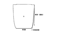
DRIE技術では、シリコン(および同様に最も一般的な材料)に深い溝(トレンチ)をエッチングすることはある垂直性誤差を通常伴い、これは、深さによるエッチングレート(速度)の変化により垂直面は100%垂直ではないことを意味する。たとえば、DRIEを使ったシリコン(Si)の典型的なエッチングプロファイルを図1Aに示す。このプロファイルは、図1Bに示すあるティルト角αをもつ直線プロファイルで近似することができる。垂直な点線に関し小さな角度αの面が、この技術によって製造される分光計/干渉計に使用されるミラーまたはビームスプリッタの面を表す。 In DRIE technology, etching deep trenches in silicon (and also the most common material) is usually accompanied by some vertical error, which is due to changes in etch rate (velocity) with depth. Means not 100% vertical. For example, a typical etching profile of silicon (Si) using DRIE is shown in FIG. 1A. This profile can be approximated by a linear profile having a certain tilt angle α shown in FIG. 1B. The plane with a small angle α with respect to the vertical dotted line represents the plane of the mirror or beam splitter used in the spectrometer / interferometer manufactured by this technique.
溝(トレンチ)の底のオーバーエッチングは、同じ技術パラメータで製造する構造のすべてにおいて同じ方向を持つ。その結果、DRIEを使用して分光計/干渉計を作るとき、作られるミラーおよびビームスプリッタの表面は垂直方向に対しある固定の角度を持つ。しかし、この角度は、いくつかの面では正で他の面では負なので、入力ビームの位置合わせによって補償することはできない。その結果、分光計/干渉計からの出力ビームは、それらの間に角度θ(αよりずっと大きい)を持ち、分光計から得られる出力縞に有意な視認性低下が生じる。 Overetching at the bottom of the trench has the same direction in all structures manufactured with the same technical parameters. As a result, when making spectrometers / interferometers using DRIE, the mirror and beam splitter surfaces created have a fixed angle with respect to the vertical direction. However, this angle is positive in some planes and negative in others, and cannot be compensated for by input beam alignment. As a result, the output beam from the spectrometer / interferometer has an angle θ (much greater than α) between them, resulting in a significant loss of visibility in the output fringes obtained from the spectrometer.
さらに従来のMEMSベースの干渉計においては、一つのアームのビームがシリコン(または他の材料)を通り、第2のアームにおけるビームが典型的には空気を通り、Si材料は(他の材料と同様に)波長とともに変化する屈折率を持ち得るので、分光計出力で得られる信号に位相誤差が導入され得る。したがって、DC成分を取り除いた後の信号は、次の式1のようになるのではなく、出力信号は、式2のようになる。

ここで、B(σ)は波数σの関数として測定される照射のスペクトル分布であり、χは光路差であり、位相誤差ψ(σ)が分光計に存在する。 Here, B (σ) is the spectral distribution of irradiation measured as a function of wave number σ, χ is the optical path difference, and phase error ψ (σ) exists in the spectrometer.
B(σ)は負の周波数を含むよう拡張することができるので、実の物理的スペクトラムを想定すると、B(σ)= B(-σ) となる。こうして、分散のないMEMSベースの分光計では、出力信号は次の式で表すことができる。
簡単なフーリエコサイン変換は、次の形のスペクトルを与えるに十分である。
しかし、分光計が分散効果を受けると、スペクトルは複雑なフーリエ変換だけから得ることになる。ψ(σ)= - ψ(-σ)であるならば、B(σ)ejψ(σ) はI(χ)の複雑なフーリエ変換であり、次の式で表される。
こうしてスペクトルは、(2サイドの)サインおよびコサイン積分の二乗の和の平方根で与えられる。
![]()
![]()
この発明の実施例によると、マイクロ・エレクトロメカニカル・システム(MEMS)分光計/干渉計について均衡した構造が使用され、ミラーおよびビームスプリッタ壁を作るのに使われるDRIEプロセスにおけるティルト角または垂直性が両アームにおいて補償され、一つのアームにおける分散が第2のアームにおける分散とバランスする。例示的な実施例は幾何的なバランス界面を使い、光干渉計の2つのアームが実質的に同じ垂直性のミラーおよびビームスプリッタを持つことができるようにし、これにより分光計出力に得られる縞の視認性を改善させ、挿入ロスを低減しスループットを増大させ分光計の解像度を改善する。もう一つの例示的実施例では、バランス界面が分光計の2つのアームの間のバランスをとり、一つのアームに存在する波長依存の位相シフトが第2のアームに導入され分光計における分散を補償する。 According to an embodiment of the present invention, a balanced structure is used for a micro electromechanical system (MEMS) spectrometer / interferometer, and tilt angle or perpendicularity in the DRIE process used to create the mirror and beam splitter walls. Compensated in both arms, the dispersion in one arm balances with the dispersion in the second arm. Exemplary embodiments use a geometric balance interface, two arms of the optical interferometer to be able to have a mirror and the beam splitter substantially the same perpendicularity, thereby resulting in the spectrometer output fringe Improved visibility, reduced insertion loss, increased throughput and improved spectrometer resolution. In another exemplary embodiment, the balance interface balances between the two arms of the spectrometer and a wavelength dependent phase shift present in one arm is introduced in the second arm to compensate for dispersion in the spectrometer. To do.
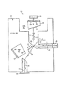
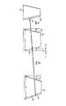
図3Aおよび3Bは、この発明の実施例による例示的な補償されたMEMSベースの分光計構造10を示す。補償されたMEMSベースの分光計10は、たとえばフーリエ変換紫外線(FTIR)干渉計であることができる。分光計10はMEMSで作動される可動ミラーを許容するSOIウェハで実現される。
3A and 3B show an exemplary compensated MEMS-based
図3Aおよび3Bにおいて、光源20が入射光ビームL1を生成し、これが入力ファイバ溝25を通って補償されたMEMSベースの分光計10に入る。入射ビームL1は入力ファイバ溝25を通って、第1媒体(すなわち、シリコン(Si)40)と第2媒体(すなわち、空気45)との界面に形成される半平面ビームスプリッタ30に至る。シリコン/空気界面ビームスプリッタ30は入射ビームからある角度(たとえば、45度)で配置されている。所望の角度は、入力ファイバ溝25近くのシリコン媒体40の面S3をリソグラフ的に規定することにより生成される。
In FIGS. 3A and 3B, the
半平面ビームスプリッタ30に衝突すると、入射ビームL1は2つの干渉ビームL2およびL4に分割される。L2は、シリコン/空気半平面ビームスプリッタ30からの入射ビームL1の部分反射から生じ、ビームの入射角に等しい反射角を持つ。L4はシリコン/空気半平面ビームスプリッタ30を通る入射ビームL1の部分伝播から生じ、ある屈折角(スネルの法則によって決まる)でシリコン40の中を伝播する。その結果、L2がミラーM1に向かって空気45中を伝播し、L4がミラーM2に向かってシリコン40中を伝播する。
When colliding with the half-
ミラーM1はシリコン媒体40のもう一つの面S5上にビームL2に垂直な角度で形成されている。特にミラーM1は、L2がシリコン40の面S1に衝突するまでまず空気40を通って伝播し、次いでシリコン媒体40を通って伝播してミラーM1に到達するよう、L2の伝播の方向に関して位置づけられている。同様にミラーM2は、シリコン媒体40のもう一つの面S4上にビームL4に垂直な角度で形成されている。しかし、M2は、L4がシリコン媒体40の面S2に達するまでまずシリコン40を通って伝播し、次いで空気45を介して伝播しミラーM2に到達するよう、L4の伝播方向に関して位置づけられている。ビームL2は、ミラーM1で反射され反射ビームL3を生成し、ビームL4は、ミラーM2で反射され反射ビームL5を生成する。図3Aに示すように、それぞれミラーM1およびM2から反射した後、両ビームL3およびL5は半平面ビームスプリッタ30に向かって、それぞれL2およびL4と同じ光路をとる(反対方向に)。こうして、分光計/干渉計がフーリエ変換(FT)分光計として使用される実施例では、一つの干渉計アームがビームL2/L3によって形成され、ビームスプリッタ30およびミラーM1を含み、もう一つの干渉計アームがビームL4/L5で形成され、ミラーM2を含む。
The mirror M1 is formed on the other surface S5 of the
ビームスプリッタ30で干渉がはじまり、干渉パターンL6が反射ビームL3およびL5から生成される。干渉パターンL6は出力ファイバ溝50を介して出力され検出平面(検出器)60によって検出される。一つの実施例では、検出器60は、光検出器を含み、これは、基板の表面を微細加工する(たとえば、基板の表面をエッチングして光り検出器を配置する開口を実現する)ことによって組み立てられるか、またはドーピング(たとえば、P―I―Nダイオードを実現するため)または部分的なメタライゼーション(たとえば、金属―半導体―金属 MSM光検出器を実現するため)を介して基板内にモノリシック的に実現される。
Interference starts at the
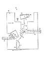
図3Aに示す例示的な実施例では、ミラーM1はSOI静電MEMSアクチュエータ70を使って可動であり、図3BではミラーM2が静電MEMSアクチュエータ70を使用して可動である。たとえば、一つの実施例では、静電MEMSアクチュエータ70は、くし形ドライブおよびばねで形成されている。キャパシタンスを有するくし形ドライブに電圧を加えることにより、アクチュエータ70に電位差が生じて駆動力が発生するとともにばねから復元力が発生し、ビームL2またはL4を反射させる所望の位置への可動ミラーM1またはM2の変位を生じさせる。ミラーM1またはM2のどちらが可動であろうと、ミラー変位の2倍に実質的に等しいL3、L5間の光路長差を達成することができる。
In the exemplary embodiment shown in FIG. 3A,
一つの実施例では、ミラーM1およびM2が金属ミラーであり、ビームスプリッタを保護するために選択的メタライゼーション(たとえば、メタライゼーションステップ中にシャドウマスクを使用する)が使われる。もう一つの実施例では、小さなフットプリント分光計を得るために非金属の垂直ブラッグ(Bragg)ミラーが使用される。ブラッグミラーは、深反応性イオンエッチング(DRIE)を使って連続的な垂直シリコン/空気界面を生成することにより実現することができる。さらに、ブラッグミラーは、簡単な反射器として作用するために広いスペクトル反射応答を持つように設計することができ、または応用によっては波長選択応答を持つように設計することができる。 In one embodiment, mirrors M1 and M2 are metal mirrors, and selective metallization (eg, using a shadow mask during the metallization step) is used to protect the beam splitter. In another embodiment, a non-metallic vertical Bragg mirror is used to obtain a small footprint spectrometer. Bragg mirrors can be realized by using deep reactive ion etching (DRIE) to create a continuous vertical silicon / air interface. In addition, the Bragg mirror can be designed to have a broad spectrum reflection response to act as a simple reflector, or it can be designed to have a wavelength selective response, depending on the application.
ビームスプリッタとしてシリコン/空気界面を説明したが、半波平面ビームスプリッタを提供するその他の材料を使ってこの発明を実現することができる。たとえば、他の例示的実施例では、微細加工のまたは組み立てられたガラス半平面またはパイレックス(Pyrex)のようなその他の材料をシリコンの代わりに使いより広い動作スペクトルウィンドウをつくることができる。さらに、液体または異なるガスのような他の材料を空気の代わりに使い、半平面ビーム分割界面の反射率を修正する自由度を提供することができる。 Although the silicon / air interface has been described as a beam splitter, the present invention can be implemented using other materials that provide a half-wave planar beam splitter. For example, in other exemplary embodiments, microfabricated or assembled glass half-planes or other materials such as Pyrex can be used in place of silicon to create a wider operating spectral window. In addition, other materials such as liquids or different gases can be used in place of air to provide the freedom to modify the reflectivity of the half-plane beam splitting interface.
使用する材料のタイプに拘わらず、2つのビームL2/L3およびL4/L5は第1の媒体40および第2の媒体45の両方を通るので、構造の寸法は、2つのビームL2/L3およびL4/L5が媒体(シリコン40)中で等距離を通るよう調整することができる。これにより、干渉計の機能性において材料(すなわちSi)の分散を実質的に完全に補償することができる。等しく2つの光路に位相誤差が導入されるからである。
Regardless of the type of material used, the two beams L2 / L3 and L4 / L5 pass through both the
たとえば、図4に示すようにミラーM1をシリコン40の表面S5に形成し、ミラーM2をシリコン40の表面S4に形成すると、ビームL2/L3はシリコン40の距離d1(すなわち、ある厚み)を通り、ビームL4/L5はシリコン40の距離d2(すなわち、ある厚み)を通る。この発明の実施例では、シリコン中のビーム分散を補償するためにd1が実質的にd2に等しい(すなわち、d1=d2)。こうして、表面S3/S2/S4および表面S3/S1/S5がバランスする界面を形成し、ビームL3とL5との間のそれぞれの位相誤差における相違を最小にする設計となる。
For example, as shown in FIG. 4, when the mirror M1 is formed on the surface S5 of the
さらに、図4に示すように、ビームスプリッタ30および2つのミラーM1およびM2は、それぞれ実質的に同じ方向に実質的に同じ垂直性(ティルト角α)を持つ。したがって、DRIE技術における垂直誤差または存在するティルト角に拘わらず、分光計の実効表面S2、S4およびS5のすべてが平行である。したがって、表面S3/S2/S4および表面S3/S1/S5によって形成されるバランス界面が実効表面間のティルト角の相違をも最小化する。分光計/干渉計における2つの他の表面S1およびS2からの反射は、表面S1およびS2の方向付けを使って避けることができ、表面S1およびS2から反射されたビームが異なる方向に向くようにする。しかし、表面S1およびS2は、分光計/干渉計10の挿入ロスを増大させ得る。この挿入ロスを低減するために表面S1およびS2がビームL1およびL2にそれぞれ直角になるようフォトリソグラフ的に規定するか、反射防止(AR)コーティングを行うことができる。
Further, as shown in FIG. 4, the
さらに、誘電体界面からの伝播角が波長に依存することから生じる2つの反射したビームL3とL5との間の角度を最小にするよう、表面S1およびS2の方向を設計することができる。角度分散は、表面S1およびS2の方向を調整して、動作レンジにおけるすべての波長が2つの反射ビームL3とL5との間でほぼ同じ角度を持つようにすることにより最小にすることができる。こうして、干渉計スペクトル応答は視認性および挿入ロスの点でよりよい均一性を持つ。 Furthermore, the direction of the surfaces S1 and S2 can be designed to minimize the angle between the two reflected beams L3 and L5 resulting from the propagation angle from the dielectric interface being wavelength dependent. Angular dispersion can be minimized by adjusting the direction of the surfaces S1 and S2 so that all wavelengths in the operating range have approximately the same angle between the two reflected beams L3 and L5. Thus, the interferometer spectral response has better uniformity in terms of visibility and insertion loss.
例示的実施例では、シリコン媒体40の表面S2は、ビームスプリッタ30と平行であ
るかまたはある角度を持つことがある。S2がビームスプリッタ表面S3と平行であるならば、S2とビームスプリッタ表面S3との間のファブリ・ペロー(Fabry-Perot)効果は、ビームスプリッタ30の表面を入射ビームL1の入力スポットのサイズ70に制限し、ビームスプリッタ表面S3とS2との間の分離を調整して、図5に示すように表面S2からの反射ビームがビームスプリッタ表面S3に面しないようにすることにより解消することができる。図5において、表面S2からの反射ビームL7はビームスプリッタ表面S3に面しないので、ファブリ・ペロー効果は実質的に解消される。
In an exemplary embodiment, the surface S2 of the
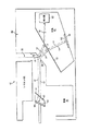
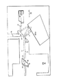
図6Aおよび6Bを参照すると、表面S2は検出器60への出力方向付けのための界面としても使用することができる。たとえば、図6Aおよび6Bに示されるように、干渉パターンL6が表面S2によって検出器60に向けられることができる。図6Aおよび6Bでは、検出器はミラーM2の近くに配置されており、干渉パターンL6が表面S2で検出器60に向けて屈折してミラーM2からは遠ざかる。この構造は、ミラーM1が可動か(図6Aに示すように)、M2が可動(図6Bに示すように)とすることにより可能である。
Referring to FIGS. 6A and 6B, the surface S2 can also be used as an interface for output orientation to the
例示的な動作では、入射ビームL1が補償されたMEMSベースの分光計10に入力ファイバ溝25を通って入り、表面S3に形成された半平面ビームスプリッタ30に達するまで入力ファイバ溝25を通って伝播する。半平面ビームスプリッタ30に衝突すると、入射ビームL1は、2つの干渉ビームL2およびL4に分割される。L2がミラーM1に向かって空気中を伝播し、L4がミラーM2に向かってシリコン40の中を伝播する。特にL2はシリコン40の表面S1に衝突するまでまず空気40中を伝播し、次いでシリコン媒体40を伝播し、ミラーM1に達する。L4は、シリコン媒体40の表面S2に達するまでまずシリコン40を伝播し、次いで空気45を伝播してミラーM2に達する。
In an exemplary operation, the incident beam L1 enters the compensated MEMS-based
ビームL2がミラーM1で反射して反射ビームL3を生成し、ビームL3がミラーM2で反射して反射ビームL5を生成する。ビームL3およびL5はそれぞれミラーM1およびM2から反射した後に両方とも同じ光路(反対方向に)をとり、半平面ビームスプリッタ30に向けてもどる。反射ビームL3およびL5がビームスプリッタ30で干渉した結果として生成される干渉パターンL6がシリコン40を伝播し表面S2に達し、検出器60に向けて屈折する。
The beam L2 is reflected by the mirror M1 to generate a reflected beam L3, and the beam L3 is reflected by the mirror M2 to generate a reflected beam L5. Beams L3 and L5 both take the same optical path (in the opposite direction) after being reflected from mirrors M1 and M2, respectively, and return to half-
図7は、垂直性および分散問題の部分的な補償をもたらすMEMSベースの分光計10のためのもう一つの構造を示す。さらに図7の構造は、表面S1およびS2から生成される挿入ロスを図3Aおよび3Bの構造に比較して低減する。たとえば、図7において、ミラーM2のメタライゼーションが取り除かれ、表面S2が不完全な反射器として使われ(すなわち、シリコン40と空気45との間の屈折率の相違を使用し)実効的ミラーM2となる。この構造では、2つの厚み(図4に示すd1およびd2)は、空気伝播に対応する位相シフトを許容するように等しくなくてよく、したがって部分的な分散補償しか生成しない。さらに、2つのミラーM1およびM2は完全には平行でなく(すなわち、ティルト角が異なる方向を向いている)、不完全なティルト角補償しか生成しない。
FIG. 7 shows another structure for a MEMS-based
例示的な動作において、入射ビームL1が一部補償されたMEMSベースの分光計10に入力ファイバ溝25を通って入り、入力ファイバ溝25を伝播して表面S3に形成された半平面ビームスプリッタ30に達する。半平面ビームスプリッタ30に衝突すると、入射ビームL1は2つの干渉ビームL2およびL4に分割される。L2が空気45中をミラーM1に向かって伝播し、L4がシリコン40中を表面/ミラーS2/M2に向かって伝播する。特に、L2はまず空気45中をシリコン40の表面S1に衝突するまで伝播し、次いでシリコン媒体40を伝播してミラーM1に達する。L4はシリコン40を伝播してシリコン媒体40の表面/ミラーS2/M2に達する。
In an exemplary operation, the incident beam L1 enters the partially compensated MEMS-based
ビームL2がミラーM1で反射されて反射ビームL3を生成し、ビームL4が表面/ミラーS2/M2で反射されて反射ビームL5を生成する。ビームL3およびL5は、反射された後、両方とも同じ光路(反対方向に)をとり、半平面ビームスプリッタ30に向かう。反射ビームL3およびL5がビームスプリッタ30で干渉して生成される干渉パターンL6がシリコン40を伝播して出力ファイバ溝50を介して検出器60に向けて出力される。
Beam L2 is reflected by mirror M1 to produce reflected beam L3, and beam L4 is reflected by surface / mirror S2 / M2 to produce reflected beam L5. Beams L3 and L5, after being reflected, both take the same optical path (in the opposite direction) and head toward half-
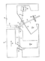
次に図8を参照すると、もう一つの一部補償されたMEMSベースの分光計10が示されている。図8において、表面S2は部分的反射器(S2/M2)として作用するだけでなく、干渉パターンL6を表面S2とS3との間の完全内部反射を介して検出器に導く。
Referring now to FIG. 8, another partially compensated MEMS-based
例示的な動作において、入射ビームL1が入力ファイバ溝25を介して一部補償されたMEMSベースの分光計10に入り、入力ファイバ溝25を伝播して表面S3に形成された半平面ビームスプリッタ30に達する。半平面ビームスプリッタ30に衝突すると、入射ビームL1は2つの干渉ビームL2およびL4に分割される。L2が空気45中をミラーM1に向かって伝播し、L4がシリコン40を表面/ミラーS2/M2に向かって伝播する。特に、L2はまず空気45を伝播してシリコン40の表面S1に衝突し、次いでシリコン媒体40を伝播してミラーM1に達する。L4はシリコン40を伝播してシリコン媒体40の表面/んミラーS2/M2に達する。
In an exemplary operation, the incident beam L1 enters the partially compensated MEMS-based
ビームL2がミラーM1で反射されて反射ビームL3を生成し、ビームL4が表面/ミラーS2/M2で反射されて反射ビームL5を生成する。ビームL3およびL5は、反射後、同じ光路を(反対方向に)とって半平面ビームスプリッタ30に向かう。ビームL3およびL5がビームスプリッタ30で干渉して生成される干渉パターンL6がシリコン40を伝播して表面/ミラーS2/M2に達し、S3とS2との間の完全内部反射によって反射され、出力ファイバ溝50を介して検出器60に向けて出力される。
Beam L2 is reflected by mirror M1 to produce reflected beam L3, and beam L4 is reflected by surface / mirror S2 / M2 to produce reflected beam L5. After reflection, the beams L3 and L5 follow the same optical path (in the opposite direction) toward the half-
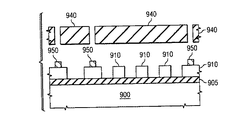
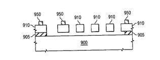
補償されたMEMSベースの分光計の例示的な製造プロセスを図9A―9Iに示す。図9Aにおいて、アルミニウムのスパッタリング工程がSOIウェハ(層900―910)に行われてアルミニウム層915が形成され、この層は、図9Eに示すようにDRIEを使ってSOIウェハの頂部シリコン層910をエッチングするためのマスクとして機能する。図9Bにおいて、フォトレジスト材料920がアルミニウム層上にスピン被覆される。図9Cにおいて、ミラー、半平面ビームスプリッタ、ファイバ溝、検出器および静電アクチュエータを実現するためにリソグラフィ工程が実施される。フォトレジスト材料920におけるリソグラフィパターンが、図9Dに示すようにアルミニウム層のプラズマ塩素エッチングによってアルミニウムマスク915に移される。次いで図9E似示すようにSOIのエッチストップ層905に達するまで、DRIEをウェハに実施する。次いで、図9Fに示すように、Aluエッチを使用して残りのアルミニウムマスク915を取り除く。
An exemplary manufacturing process for a compensated MEMS-based spectrometer is shown in FIGS. 9A-9I. In FIG. 9A, an aluminum sputtering process is performed on an SOI wafer (layers 900-910) to form an
図9Iを参照すると、マイクロミラーおよび反射面の選択的メタライゼーションのためおよび接続パッド形成のために、シャドウマスク940が使用される。図9Iに見られるように、シャドウマスク940は、頂部のシリコン層910の所望の部分にCr/Au950を選択的にスパッタするために、SOI基板900―910の上方に配置される。ブラッグミラー(Bragg mirror)のような非金属のミラーを使う実施例では、シャドウマスク工程は実施されず、パッドのメタライゼーションは、残りのプロセス工程で耐えられるだけ強いメタライゼーション厚みが得られるならば、はじめに実施することができる。図9Jに示されるように、くし形のフィンガー、ばね、および可動ミラーのような可動構造がHFを使って埋め込みSiO2層をエッチングすることによって解放され、固定の構造は下のSiO2が広い面積なので解放されない。くし形の駆動アクチュエータを説明したが、可動ミラーは相性のよい技術によって製造される任意のMEMSアクチュエータを使って作動させることができる。たとえば、アクチュエータは、同じマスクで同じ先の工程を使って分光計と共に製造することができる。
Referring to FIG. 9I, a
DRIEエッチングにボッシュ(Bosch)プロセスを使用する実施例においては(図9E)、このプロセスの期間的な性質によりミラー面が荒くなることがある。したがって、図9Gに示すように、表面に厚い酸化層930を成長させ、次いで図9Hに示すようにHFによってこれを取り除き、構造を貴方する前にミラー面を滑らかにすることが有用である。しかし、高温度アニーリング、エッチングまたは酸化のような任意の使用可能な技法を使って光学表面の平滑化を行うことができることが理解されねばならない。低温のDRIEプロセスを図9Eにおいて使用するならば、エッチング後に滑らかな表面が得られるので、図9Gおよび9Hに示すプロセス工程は必要ないであろう。さらに、このプロセスは低温度においてフォトレジスト材料とシリコンとの間でよい選択性を持つので、図9Aに示すアルミニウムマスクは必要ない。
In embodiments that use the Bosch process for DRIE etching (FIG. 9E), the mirror surface may be rough due to the temporal nature of the process. Therefore, it is useful to grow a
当業者には明らかなように、この明細書に記載した革新的概念は、広いレンジの応用において修正市変更することができる。したがって、この発明の範囲は上述した特定の例示的な教示によって限定されてはならず、特許請求の範囲によって規定される。 As will be apparent to those skilled in the art, the innovative concepts described herein can be modified in a wide range of applications. Accordingly, the scope of the invention should not be limited by the specific exemplary teachings described above, but is defined by the claims.
Claims (21)
第1媒体の、第2媒体との界面にある第1の表面に形成され、当該第1の表面への入射ビームを前記第1媒体中を伝播する第1干渉ビームおよび前記第2媒体中を伝播する第2干渉ビームに分割するビームスプリッタと、
前記第1干渉ビームを反射するように、前記第1媒体の第2の表面に形成された第1のミラーと、
前記第2干渉ビームを反射するように、前記第1媒体の第3の表面に形成された第2のミラーと、
前記第1干渉ビームの光路内および前記第2干渉ビームの光路内に設けられた前記第1媒体の付加的な表面と、
前記第1のミラーにより反射された前記第1干渉ビームと前記第2のミラーにより反射された前記第2干渉ビームとの間の干渉により生成された干渉パターンを検出するよう光学的に結合された検出器と、
前記第1および第2のミラーの一つに変位を生じさせるよう結合された静電アクチュエータであって、前記変位により、前記第1干渉ビームと前記第2干渉ビームとの間に前記変位の2倍に等しい光路長差を生成する静電アクチュエータと、
を備え、
前記第1干渉ビームの光路内には、第2干渉ビームの光路内の第1媒体のそれぞれの表面に対応する第1媒体の表面であって、当該それぞれの表面と同じ方向に同じ大きさのティルト角を持って且つ当該それぞれの表面と同じ反射又は透過の機能を持つ対応する表面が存在するよう構成されており、
前記第2干渉ビームの光路内に設けられた前記付加的な表面の少なくとも一つは、第1干渉ビームと第2干渉ビームとの間のそれぞれの位相誤差における相違を最小化するために前記第2干渉ビームの光路内に配置された第1媒体のブロックの表面である、
干渉計。 A micro electro mechanical system (MEMS) interferometer, comprising:
A first interference beam formed on a first surface of the first medium at the interface with the second medium and propagating an incident beam on the first surface in the first medium and in the second medium A beam splitter for splitting into a propagating second interference beam;
A first mirror formed on a second surface of the first medium to reflect the first interference beam;
A second mirror formed on a third surface of the first medium to reflect the second interference beam;
An additional surface of the first medium provided in the optical path of the first interference beam and in the optical path of the second interference beam;
Optically coupled to detect an interference pattern generated by interference between the first interference beam reflected by the first mirror and the second interference beam reflected by the second mirror; A detector;
An electrostatic actuator coupled to cause a displacement in one of the first and second mirrors, wherein the displacement causes a displacement of 2 between the first interference beam and the second interference beam; An electrostatic actuator that produces a path length difference equal to twice,
With
In the optical path of the first interference beam, the surface of the first medium corresponding to the surface of the first medium in the optical path of the second interference beam, and having the same size in the same direction as the respective surface A corresponding surface having a tilt angle and having the same reflection or transmission function as the respective surface,
At least one of the additional surfaces provided in the optical path of the second interference beam may be configured to minimize the difference in the respective phase error between the first interference beam and the second interference beam. 2 is a surface of a block of a first medium arranged in the optical path of the interference beam,
Interferometer.
基板を構成する頂部層および底部層を含むシリコンオンインシュレータ(SOI)ウェハをさらに備え、
前記ビームスプリッタ、前記第1のミラー、前記第2のミラー、前記付加的な表面および前記静電アクチュエータが、前記SOIウェハの頂部表面に形成されており、
前記静電アクチュエータと、該静電アクチュエータに結合された前記第1および第2のミラーの前記一つとは、前記SOIウェハの底部層から分離されている、
請求項1に記載の干渉計。 The first medium is silicon and the second medium is air;
A silicon-on-insulator (SOI) wafer including a top layer and a bottom layer constituting the substrate;
The beam splitter, the first mirror, the second mirror, the additional surface and the electrostatic actuator are formed on a top surface of the SOI wafer;
The electrostatic actuator and the one of the first and second mirrors coupled to the electrostatic actuator are separated from a bottom layer of the SOI wafer;
The interferometer according to claim 1.
前記静電アクチュエータと、該静電アクチュエータに結合された前記第1および第2のミラーの前記一つとを、前記SOIウェハの頂部層と底部層との間のエッチングによって形成する、Forming the electrostatic actuator and the one of the first and second mirrors coupled to the electrostatic actuator by etching between a top layer and a bottom layer of the SOI wafer;
請求項2に記載の干渉計を製造する方法。A method of manufacturing the interferometer according to claim 2.
請求項2に記載の干渉計を作製する方法。 The first, second, third surface and the additional surface are each formed by etching a portion of the top surface of the SOI wafer using a deep reactive ion etching (DRIE) process. ,
A method for producing the interferometer according to claim 2.
第1の干渉計アームにおいて、
前記第1媒体の第1区分は、前記ビームスプリッタが形成される前記第1の表面を持ち、
前記第1媒体の前記第2の表面に前記第1のミラーが形成されており、
第2の干渉計アームにおいて、
前記ブロックである前記第1媒体の第2区分は、前記第2のミラーが形成される前記第3の表面と、前記付加的な表面の一つとを持ち、該付加的な表面の一つは前記第3の表面に対向して前記第2干渉ビームを当該第3の表面に向かわせ、
前記ビームスプリッタ、前記第1のミラー、および前記第2のミラーのそれぞれの、基板との間のティルト角が、すべて同じである、請求項1に記載の干渉計。 The interferometer is used as a Fourier Transform (FT) spectrometer,
In the first interferometer arm:
A first section of the first medium has the first surface on which the beam splitter is formed;
The first mirror is formed on the second surface of the first medium;
In the second interferometer arm:
The second section of the first medium that is the block has the third surface on which the second mirror is formed and one of the additional surfaces, one of the additional surfaces being Directing the second interference beam to the third surface opposite the third surface;
The interferometer according to claim 1, wherein each of the beam splitter, the first mirror, and the second mirror has the same tilt angle with respect to the substrate.
請求項7に記載の干渉計。 The first section includes the second surface, and the first surface faces the second surface of the first section such that the second interference beam is internally reflected within the first section. Arranged,
The interferometer according to claim 7 .
請求項9に記載の干渉計。 The first mirror is formed on the second surface such that a portion of the first mirror functions as a partial internal reflector;
The interferometer according to claim 9 .
前記第1区分は、さらに、前記付加的な表面の一つを含み、前記付加的な表面の当該一つは、前記第1の表面と対向し、前記第1干渉ビームを前記第2の表面へ導く、
請求項7に記載の干渉計。 The first interferometer arm further has a third section of the first medium separated from the first section by an area of the second medium, the third section having the second surface; And,
The first section further includes one of the additional surfaces, the one of the additional surfaces facing the first surface, and directing the first interference beam to the second surface. Lead to the
The interferometer according to claim 7 .
前記第1干渉ビームが、前記一つの反射、屈折表面から前記入射ビームが一部屈折して生成され、
前記第2干渉ビームが、前記一つの反射、屈折表面から前記入射ビームが一部反射されて生成される、請求項1に記載の干渉計。 The beam splitter comprises a reflective, refractive surface that forms an interface between the first medium and the second medium;
The first interference beam is generated by partially refracting the incident beam from the one reflecting and refracting surface,
The interferometer according to claim 1, wherein the second interference beam is generated by partially reflecting the incident beam from the one reflection / refractive surface.
前記検出器に前記干渉パターンを提供するよう光結合した出力ファイバ溝と、
をさらに備える、請求項1に記載の干渉計。 An input fiber groove optically coupled to provide an incident beam to the beam splitter;
An output fiber groove optically coupled to provide the interference pattern to the detector;
The interferometer according to claim 1, further comprising:
Applications Claiming Priority (3)
| Application Number | Priority Date | Filing Date | Title |
|---|---|---|---|
| US24053109P | 2009-09-08 | 2009-09-08 | |
| US61/240,531 | 2009-09-08 | ||
| PCT/US2010/048169 WO2011031791A1 (en) | 2009-09-08 | 2010-09-08 | Compensated mems ftir spectrometer architecture |
Publications (3)
| Publication Number | Publication Date |
|---|---|
| JP2013504066A JP2013504066A (en) | 2013-02-04 |
| JP2013504066A5 JP2013504066A5 (en) | 2014-12-18 |
| JP5860809B2 true JP5860809B2 (en) | 2016-02-16 |
Family
ID=43063959
Family Applications (1)
| Application Number | Title | Priority Date | Filing Date |
|---|---|---|---|
| JP2012528127A Active JP5860809B2 (en) | 2009-09-08 | 2010-09-08 | Microelectromechanical system (MEMS) interferometer |
Country Status (5)
| Country | Link |
|---|---|
| US (1) | US8531675B2 (en) |
| EP (1) | EP2475970B1 (en) |
| JP (1) | JP5860809B2 (en) |
| SG (1) | SG179018A1 (en) |
| WO (1) | WO2011031791A1 (en) |
Families Citing this family (12)
| Publication number | Priority date | Publication date | Assignee | Title |
|---|---|---|---|---|
| JP2012107962A (en) * | 2010-11-16 | 2012-06-07 | Konica Minolta Holdings Inc | Interferometer and spectrograph equipped with the same |
| FR2985809B1 (en) * | 2012-01-16 | 2015-12-25 | Laboratoire Nat De Metrologie Et Dessais | INTERFEROMETRIC OPTICAL PROBE OF DIMENSIONAL MEASUREMENT |
| US8922787B2 (en) * | 2013-01-07 | 2014-12-30 | Si-Ware Systems | Spatial splitting-based optical MEMS interferometers |
| CN105890758B (en) * | 2014-12-31 | 2018-06-15 | 南开大学 | Miniature Fourier infrared spectrometer that is a kind of while using MEMS translations and torsion mirror |
| US9970819B2 (en) | 2015-03-23 | 2018-05-15 | Si-Ware Systems | High performance parallel spectrometer device |
| JP6026597B1 (en) * | 2015-07-06 | 2016-11-16 | 浜松ホトニクス株式会社 | Optical interferometer |
| JP5839759B1 (en) * | 2015-07-30 | 2016-01-06 | 浜松ホトニクス株式会社 | Optical interferometer |
| JP6943452B2 (en) * | 2016-06-15 | 2021-09-29 | シーウェア システムズSi−Ware Systems | Integrated spectrum unit |
| JP6704833B2 (en) * | 2016-10-27 | 2020-06-03 | 浜松ホトニクス株式会社 | Position detection method and optical module |
| US11841268B2 (en) | 2021-02-02 | 2023-12-12 | Si-Ware Systems | Compact material analyzer |
| US11635369B1 (en) | 2021-11-02 | 2023-04-25 | Saudi Arabian Oil Company | Miniature FT-MIR using a MEMS interferometer with a metasurface emitter and detector |
| US11774289B2 (en) | 2021-11-02 | 2023-10-03 | Saudi Arabian Oil Company | Micro-electromechanical system (MEMS) interferometer for FT-MIR spectroscopy |
Family Cites Families (6)
| Publication number | Priority date | Publication date | Assignee | Title |
|---|---|---|---|---|
| US3443871A (en) * | 1965-12-07 | 1969-05-13 | Optomechanisms Inc | Single optical block interferometer means |
| US4278351A (en) * | 1979-05-09 | 1981-07-14 | Nasa | Interferometer |
| US4735505A (en) * | 1983-08-30 | 1988-04-05 | The Perkin-Elmer Corporation | Assembly for adjusting an optical element |
| US6967722B2 (en) * | 1997-10-28 | 2005-11-22 | Manning Christopher J | Tilt-compensated interferometers |
| US6952266B2 (en) * | 2003-01-15 | 2005-10-04 | Inlight Solutions, Inc. | Interferometer alignment |
| US7796267B2 (en) * | 2006-09-28 | 2010-09-14 | Si-Ware Systems | System, method and apparatus for a micromachined interferometer using optical splitting |
-
2010
- 2010-09-08 US US12/877,888 patent/US8531675B2/en active Active
- 2010-09-08 JP JP2012528127A patent/JP5860809B2/en active Active
- 2010-09-08 SG SG2012015855A patent/SG179018A1/en unknown
- 2010-09-08 EP EP10755038.6A patent/EP2475970B1/en active Active
- 2010-09-08 WO PCT/US2010/048169 patent/WO2011031791A1/en active Application Filing
Also Published As
| Publication number | Publication date |
|---|---|
| WO2011031791A1 (en) | 2011-03-17 |
| US20110058180A1 (en) | 2011-03-10 |
| JP2013504066A (en) | 2013-02-04 |
| EP2475970B1 (en) | 2021-11-03 |
| EP2475970A1 (en) | 2012-07-18 |
| SG179018A1 (en) | 2012-04-27 |
| US8531675B2 (en) | 2013-09-10 |
Similar Documents
| Publication | Publication Date | Title |
|---|---|---|
| JP5860809B2 (en) | Microelectromechanical system (MEMS) interferometer | |
| JP5204450B2 (en) | System, method and apparatus for a micromachined interferometer using optical branching | |
| US8736843B2 (en) | Opto-mechanical optical path retardation multiplier for optical MEMS applications | |
| EP2941621B1 (en) | Spatial splitting-based optical mems interferometers | |
| US8873125B2 (en) | Technique to determine mirror position in optical interferometers | |
| JP5739224B2 (en) | Optical component manufacturing method and optical component | |
| JP2019522189A (en) | Integrated spectrum unit | |
| US9618323B2 (en) | Method for manufacturing optical interferometer | |
| JP2013504066A5 (en) | ||
| CN111936831A (en) | Self-reference spectrometer | |
| US9970819B2 (en) | High performance parallel spectrometer device | |
| US8081319B2 (en) | Adjustable two dimensional lamellar grating | |
| US8508745B2 (en) | System, method and apparatus for a micromachined interferometer using optical splitting | |
| JP6711993B2 (en) | Self-calibration for mirror positioning in an optical MEMS interferometer | |
| Farrugia et al. | A concave moems scanning diffraction grating for infrared micro-spectrometer applications |
Legal Events
| Date | Code | Title | Description |
|---|---|---|---|
| A621 | Written request for application examination |
Free format text: JAPANESE INTERMEDIATE CODE: A621 Effective date: 20130903 |
|
| A977 | Report on retrieval |
Free format text: JAPANESE INTERMEDIATE CODE: A971007 Effective date: 20140318 |
|
| A131 | Notification of reasons for refusal |
Free format text: JAPANESE INTERMEDIATE CODE: A131 Effective date: 20140422 |
|
| A601 | Written request for extension of time |
Free format text: JAPANESE INTERMEDIATE CODE: A601 Effective date: 20140718 |
|
| A602 | Written permission of extension of time |
Free format text: JAPANESE INTERMEDIATE CODE: A602 Effective date: 20140728 |
|
| A601 | Written request for extension of time |
Free format text: JAPANESE INTERMEDIATE CODE: A601 Effective date: 20140821 |
|
| A602 | Written permission of extension of time |
Free format text: JAPANESE INTERMEDIATE CODE: A602 Effective date: 20140828 |
|
| A601 | Written request for extension of time |
Free format text: JAPANESE INTERMEDIATE CODE: A601 Effective date: 20140919 |
|
| A602 | Written permission of extension of time |
Free format text: JAPANESE INTERMEDIATE CODE: A602 Effective date: 20140929 |
|
| A521 | Written amendment |
Free format text: JAPANESE INTERMEDIATE CODE: A523 Effective date: 20141022 |
|
| A524 | Written submission of copy of amendment under section 19 (pct) |
Free format text: JAPANESE INTERMEDIATE CODE: A524 Effective date: 20141022 |
|
| A131 | Notification of reasons for refusal |
Free format text: JAPANESE INTERMEDIATE CODE: A131 Effective date: 20150310 |
|
| A601 | Written request for extension of time |
Free format text: JAPANESE INTERMEDIATE CODE: A601 Effective date: 20150609 |
|
| A521 | Written amendment |
Free format text: JAPANESE INTERMEDIATE CODE: A523 Effective date: 20150707 |
|
| A131 | Notification of reasons for refusal |
Free format text: JAPANESE INTERMEDIATE CODE: A131 Effective date: 20150728 |
|
| A521 | Written amendment |
Free format text: JAPANESE INTERMEDIATE CODE: A523 Effective date: 20151026 |
|
| TRDD | Decision of grant or rejection written | ||
| A01 | Written decision to grant a patent or to grant a registration (utility model) |
Free format text: JAPANESE INTERMEDIATE CODE: A01 Effective date: 20151124 |
|
| A61 | First payment of annual fees (during grant procedure) |
Free format text: JAPANESE INTERMEDIATE CODE: A61 Effective date: 20151221 |
|
| R150 | Certificate of patent or registration of utility model |
Ref document number: 5860809 Country of ref document: JP Free format text: JAPANESE INTERMEDIATE CODE: R150 |
|
| R250 | Receipt of annual fees |
Free format text: JAPANESE INTERMEDIATE CODE: R250 |
|
| R250 | Receipt of annual fees |
Free format text: JAPANESE INTERMEDIATE CODE: R250 |