JP5818000B2 - Atomic oscillator, control method of atomic oscillator, and quantum interference device - Google Patents
Atomic oscillator, control method of atomic oscillator, and quantum interference device Download PDFInfo
- Publication number
- JP5818000B2 JP5818000B2 JP2011269998A JP2011269998A JP5818000B2 JP 5818000 B2 JP5818000 B2 JP 5818000B2 JP 2011269998 A JP2011269998 A JP 2011269998A JP 2011269998 A JP2011269998 A JP 2011269998A JP 5818000 B2 JP5818000 B2 JP 5818000B2
- Authority
- JP
- Japan
- Prior art keywords
- frequency
- light
- signal
- control signal
- unit
- Prior art date
- Legal status (The legal status is an assumption and is not a legal conclusion. Google has not performed a legal analysis and makes no representation as to the accuracy of the status listed.)
- Expired - Fee Related
Links
Images


Classifications
-
- H—ELECTRICITY
- H03—ELECTRONIC CIRCUITRY
- H03B—GENERATION OF OSCILLATIONS, DIRECTLY OR BY FREQUENCY-CHANGING, BY CIRCUITS EMPLOYING ACTIVE ELEMENTS WHICH OPERATE IN A NON-SWITCHING MANNER; GENERATION OF NOISE BY SUCH CIRCUITS
- H03B17/00—Generation of oscillations using radiation source and detector, e.g. with interposed variable obturator
-
- G—PHYSICS
- G04—HOROLOGY
- G04F—TIME-INTERVAL MEASURING
- G04F5/00—Apparatus for producing preselected time intervals for use as timing standards
- G04F5/14—Apparatus for producing preselected time intervals for use as timing standards using atomic clocks
Landscapes
- Physics & Mathematics (AREA)
- General Physics & Mathematics (AREA)
- Stabilization Of Oscillater, Synchronisation, Frequency Synthesizers (AREA)
Description
本発明は、原子発振器、原子発振器の制御方法及び量子干渉装置に関する。 The present invention relates to an atomic oscillator, an atomic oscillator control method, and a quantum interference device.
図19に示すように、アルカリ金属原子は、タームシンボル2S1/2で表される基底準位と、タームシンボル2P1/2、2P3/2で表される2つの励起準位とを有することが知られている。さらに、2S1/2、2P1/2、2P3/2の各準位は、複数のエネルギー準位に分裂した超微細構造を有している。具体的には、2S1/2はI+1/2とI−1/2の2つの基底準位を持ち、2P1/2はI+1/2とI−1/2の2つの励起準位を持ち、2P3/2はI+3/2,I+1/2,I−1/2,I−3/2の4つの励起準位を持っている。ここで、Iは核スピン量子数である。 As shown in FIG. 19, the alkali metal atom has a ground level represented by a term symbol 2 S 1/2 and two excitation levels represented by term symbols 2 P 1/2 and 2 P 3/2. It is known to have Furthermore, each level of 2 S 1/2 , 2 P 1/2 , 2 P 3/2 has a hyperfine structure divided into a plurality of energy levels. Specifically, 2 S 1/2 has two ground levels, I + 1/2 and I−1 / 2, and 2 P 1/2 has two excitation levels, I + 1/2 and I−1 / 2. 2 P 3/2 has four excitation levels of I + 3/2 , I + 1/2, I−1 / 2, and I−3 / 2. Here, I is a nuclear spin quantum number.
2S1/2のI−1/2の基底準位にある原子は、D2線を吸収することで、2P3/2のI+1/2,I−1/2,I−3/2のいずれかの励起準位に遷移することができるが、I+3/2の励起準位に遷移することはできない。2S1/2のI+1/2の基底準位にある原子は、D2線を吸収することで、2P3/2のI+3/2,I+1/2,I−1/2のいずれかの励起準位に遷移することができるが、I−3/2の励起準位に遷移することはできない。これらは、電気双極子遷移を仮定した場合の遷移選択則による。逆に、2P3/2のI+1/2又はI−1/2の励起準位にある原子は、D2線を放出して2S1/2のI+1/2又はI−1/2の基底準位(元の基底準位又は他方の基底準位のいずれか)に遷移することができる。ここで、2S1/2のI+1/2,I−1/2の2つの基底準位と2P3/2のI+1/2又はI−1/2の励起準位からなる3準位(2つの基底準位と1つの励起準位からなる)は、D2線の吸収・発光によるΛ型の遷移が可能であることからΛ型3準位と呼ばれる。これに対して、2P3/2のI−3/2の励起準位にある原子は、D2線を放出して必ず2S1/2のI−1/2の基底準位(元の基底準位)に遷移し、同様に、2P3/2のI+3/2の励起準位にある原子は、D2線を放出して必ず2S1/2のI+1/2の基底準位(元の基底準位)に遷移する。すなわち、2S1/2のI+1/2,I−1/2の2つの基底準位と2P3/2のI−3/2又はI+3/2の励起準位からなる3準位は、D2線の吸収・放出によるΛ型の遷移が不可能であることからΛ型3準位を形成しない。
In I-1/2 of the ground level of 2 S 1/2 atoms, by absorbing the D2 line, the 2 P 3/2 I + 1/2 , I-1/2, the I-3/2 Transition to any of the excitation levels is possible, but it is not possible to transition to the excitation level of I + 3/2. An atom at the ground level of I +1/2 of 2 S 1/2 absorbs the D2 line, thereby exciting any of I + 3/2 , I + 1/2, I-1 / 2 of 2 P 3/2 It can transition to the level, but cannot transition to the excited level of I-3 / 2. These are based on the transition selection rule when electric dipole transition is assumed. Conversely, the atoms in the 2 P 3/2 I + 1/2 or I-1 / 2 excited level emit D2 rays and the 2 S 1/2 I + 1/2 or I-1 / 2 basis. It is possible to transition to a level (either the original ground level or the other ground level). Here, two levels of 2 S 1/2 I + 1/2 and I-1 / 2 and two levels of 2 P 3/2 I + 1/2 or I-1 / 2 excited levels ( (Consisting of two ground levels and one excitation level) is called a Λ-type three level because it can make a Λ-type transition by absorption and emission of the D2 line. On the other hand, an atom in the I-3 / 2 excited level of 2 P 3/2 emits a D2 line, and is always a 2 S 1/2 I-1 / 2 ground level (original Similarly, an atom in the excitation level of 2 P 3/2 I + 3/2 emits a D2 line, and always has an I + 1/2 ground level of 2 S 1/2 ( Transition to the original ground level). That is, three levels consisting of two ground levels of 2 S 1/2 I + 1/2 and I-1 / 2 and 2 P 3/2 I-3 / 2 or I + 3/2 excited levels, Since the Λ-type transition due to the absorption and emission of the D2 line is impossible, the Λ-
ところで、気体状のアルカリ金属原子に、Λ型3準位を形成する第1の基底準位(2S1/2のI−1/2の基底準位)と励起準位(例えば、2P3/2のI+1/2の励起準位)とのエネルギー差に相当する周波数(振動数)を有する共鳴光(共鳴光1とする)と、第2の基底準位(2S1/2のI+1/2の基底準位)と励起準位とのエネルギー差に相当する周波数(振動数)を有する共鳴光(共鳴光2とする)とを同時に照射すると、2つの基底準位の重ね合わせ状態、即ち量子コヒーレンス状態(暗状態)になり、励起準位への励起が停止する電磁誘起透過(EIT:Electromagnetically Induced Transparency)現象(CPT(Coherent Population Trapping)と呼ばれることもある)が起こることが知られている。このEIT現象を起こす共鳴光対(共鳴光1と共鳴光2)の周波数差はアルカリ金属原子の2つの基底準位のエネルギー差ΔE12に相当する周波数と正確に一致する。例えば、セシウム原子は、2つの基底準位のエネルギー差に相当する周波数は9.192631770GHzであるので、セシウム原子に、周波数差が9.192631770GHzの2種類のD1線又はD2線のレーザー光を同時に照射すると、EIT現象が起こる。
By the way, the first ground level (the I-1 / 2 ground level of 2 S 1/2 ) and the excited level (for example, 2 P) forming a Λ-type three level in a gaseous alkali metal atom. resonance light having 3/2 of I + 1/2 of the excitation level) and the frequency corresponding to the energy difference (frequency) and (a resonant light 1),
従って、図20に示すように、周波数がf1の光と周波数がf2の光を気体状のアルカリ金属原子に同時に照射したとき、この2種類の光が共鳴光対となってアルカリ金属原子がEIT現象を起こすか否かでアルカリ金属原子を透過する光の強度が急峻に変化する。この急峻に変化する透過光の強度を示す信号はEIT信号と呼ばれ、共鳴光対の周波数差f1−f2がΔE12に相当する周波数f12と正確に一致するときにEIT信号のレベルがピーク値を示す。そこで、EIT信号のピークトップを検出し、アルカリ金属原子に照射する2種類の光の周波数差f1−f2がΔE12に相当する周波数f12と正確に一致するように制御することで、高精度な発振器を実現することができる。 Accordingly, as shown in FIG. 20, when light having a frequency of f 1 and light having a frequency of f 2 are simultaneously irradiated onto a gaseous alkali metal atom, the two kinds of light become a resonance light pair to form an alkali metal atom. The intensity of light that passes through the alkali metal atom changes sharply depending on whether or not EIT occurs. A signal indicating the intensity of the transmitted light that changes sharply is called an EIT signal, and the level of the EIT signal when the frequency difference f 1 -f 2 of the resonant light pair exactly matches the frequency f 12 corresponding to ΔE 12. Indicates a peak value. Therefore, by detecting the peak top of the EIT signal and performing control so that the frequency difference f 1 -f 2 of the two types of light irradiated to the alkali metal atom exactly matches the frequency f 12 corresponding to ΔE 12 , A highly accurate oscillator can be realized.
図21は、従来のEIT方式による原子発振器の一般的な構成の概略図である。図21に示すように、従来のEIT方式による原子発振器は、電流駆動回路により発生した周波数f0(=v/λ0:vは光の速度、λ0は光の波長)を設定するための駆動電流に、周波数がfmの変調信号を重畳することにより、半導体レーザーに変調をかけて周波数がf0+fmの光と周波数がf0−fmの光を発生させる。この2種類の光はガスセルに同時に照射され、光検出器によりガスセルを透過した光の強度を検出する。ガスセルは気体状のアルカリ金属原子とこれを封入する容器とから構成されており、同時に照射された2種類の光が共鳴光対となれば、アルカリ金属原子がEIT現象を起こし、ガスセルを透過する光の強度が大きくなる。そこで、この原子発振器は、低周波発振器が発生する数十Hz〜数百Hz程度の低周波信号を用いて検波を行うことで、光検出器が検出する光の強度が最大になるように電圧制御水晶発振器(VCXO:Voltage Controlled Crystal Oscillator)の発振周波数を制御し、PLL(Phase Locked Loop)を介して周波数がfmの変調信号を生成する。このような構成によれば、半導体レーザーが出射する、周波数がf0+fmの光と周波数がf0−fmの光の周波数差2fmがΔE12に相当する周波数と一致するように、すなわち、変調信号の周波数fmがΔE12に相当する周波数の1/2の周波数と一致するように制御がかかる。従って、電圧制御水晶発振器(VCXO)の発振動作が極めて安定に継続し、周波数安定度が極めて高い発振信号を発生させることができる。
FIG. 21 is a schematic diagram of a general configuration of a conventional atomic oscillator based on the EIT method. As shown in FIG. 21, the conventional atomic oscillator according to the EIT method is for setting the frequency f 0 (= v / λ 0 : v is the speed of light and λ 0 is the wavelength of light) generated by the current driving circuit. the drive current by the frequency superimposing a modulated signal f m, frequency by modulating the semiconductor laser light and a frequency of f 0 + f m generates the light of f 0 -f m. These two types of light are simultaneously irradiated onto the gas cell, and the intensity of the light transmitted through the gas cell is detected by a photodetector. The gas cell is composed of a gaseous alkali metal atom and a container that encloses the gas. If two types of light irradiated at the same time form a resonant light pair, the alkali metal atom causes an EIT phenomenon and passes through the gas cell. The intensity of light increases. Therefore, this atomic oscillator uses a low frequency signal of about several tens Hz to several hundreds Hz generated by the low frequency oscillator to detect the voltage so that the light intensity detected by the photodetector is maximized. controlled Crystal oscillator: controlling the oscillation frequency of the (VCXO Voltage controlled Crystal oscillator), the frequency through a PLL (Phase Locked Loop) to generate a modulated signal f m. According to such a configuration, the semiconductor laser is emitted, so that the frequency of light and the frequency of f 0 + f m
ところで、従来の原子発振器では、低周波信号を用いた検波により、EIT信号のピークトップを検出し、変調信号の周波数fmがΔE12に相当する周波数の1/2の周波数と正確に一致するように制御がかかるためには、EIT信号が左右対称であることが前提となっている。逆に言えば、従来の原子発振器では、EIT信号が左右非対称であれば、変調信号の周波数fmとΔE12に相当する周波数の1/2の周波数がわずかにずれた状態で安定する可能性がある。このような状態でも、高い周波数安定度が確保され、例えば、電圧制御水晶発振器(VCXO)の発振周波数を所望の周波数に変換する回路を付加することで、周波数精度も確保できる。 Incidentally, in the conventional atomic oscillator, the detection using the low-frequency signal, detects the peak top of the EIT signal, the frequency f m of the modulation signal exactly matches the half of the frequency of the frequency corresponding to Delta] E 12 For such control to take place, it is assumed that the EIT signal is symmetrical. Conversely, in the conventional atomic oscillator, if the EIT signal is asymmetrical potential to stabilize in a state where half the frequency of the frequency corresponding to the frequency f m and Delta] E 12 of the modulated signal is slightly deviated There is. Even in such a state, high frequency stability is ensured. For example, by adding a circuit that converts the oscillation frequency of the voltage controlled crystal oscillator (VCXO) to a desired frequency, the frequency accuracy can be ensured.
ところが、周囲環境の温度の急激な変化等に起因してEIT信号のピーク値(強度)が変化して非対称の度合いが変わると、変調信号の周波数fmとΔE12に相当する周波数の1/2の周波数との差が変動し、原子発振器の周波数安定度が低下する原因となる。
However, if the peak value of the EIT signal due to such sudden changes in temperature of the surrounding environment (intensity) is changed degree of asymmetry varies, the frequency corresponding to the frequency f m and Delta] E 12 of the modulated
本発明は、以上のような問題点に鑑みてなされたものであり、本発明のいくつかの態様によれば、EIT信号の強度が変化しても高い周波数安定度を維持することが可能な原子発振器、原子発振器の制御方法及び量子干渉装置を提供することができる。 The present invention has been made in view of the above problems, and according to some aspects of the present invention, high frequency stability can be maintained even if the intensity of the EIT signal changes. An atomic oscillator, an atomic oscillator control method, and a quantum interference device can be provided.
(1)本発明は、共鳴光対によって金属原子に電磁誘起透過現象を発生させる原子発振器であって、周波数変調された制御信号を生成する制御信号生成部と、前記制御信号の周波数に応じた周波数差の第1の光と第2の光を発生させる光発生部と、前記第1の光と前記第2の光が照射される金属原子と、前記金属原子を透過した光を検出する光検出部と、前記光検出部の検出信号に基づいて、前記第1の光と前記第2の光が前記共鳴光対となるように前記制御信号の周波数を制御する周波数制御部と、前記光検出部の検出信号に応じて、前記制御信号の最大周波数偏移を制御する最大周波数偏移制御部と、を含む、原子発振器である。 (1) The present invention is an atomic oscillator that generates an electromagnetically induced transmission phenomenon in a metal atom by a resonant light pair, a control signal generation unit that generates a frequency-modulated control signal, and a frequency according to the frequency of the control signal A light generating unit that generates first light and second light having a frequency difference, a metal atom irradiated with the first light and the second light, and light that detects light transmitted through the metal atom. A detection unit; a frequency control unit configured to control a frequency of the control signal based on a detection signal of the light detection unit so that the first light and the second light become the resonance light pair; and the light An atomic oscillator including a maximum frequency deviation control unit that controls a maximum frequency deviation of the control signal in accordance with a detection signal of the detection unit.
本発明によれば、制御信号の周波数に応じた周波数差の第1の光と第2の光を金属原子に照射し、金属原子を透過した光を検出して金属原子に照射される第1の光と第3の光が金属原子に電磁誘起透過現象を発生させる共鳴光対となるように制御信号の周波数を制御する。このフィードバック制御により、第1の光と第2の光の周波数差を一定に保持することができるので、安定した周波数の発振信号を得ることができる。 According to the present invention, the first light and the second light having a frequency difference corresponding to the frequency of the control signal are irradiated to the metal atom, the light transmitted through the metal atom is detected, and the first light is irradiated to the metal atom. The frequency of the control signal is controlled so that the light and the third light form a resonant light pair that causes an electromagnetically induced transmission phenomenon in the metal atom. By this feedback control, the frequency difference between the first light and the second light can be kept constant, so that an oscillation signal having a stable frequency can be obtained.
特に、本発明では、光検出部の検出信号に応じて、制御信号の最大周波数偏移を制御することで、EIT信号強度の変化による発振信号の周波数変動分を、最大周波数偏移の変化による発振信号の周波数変動分で打ち消すことができるので、EIT信号強度が変化しても発振信号の周波数を一定に保持することができる。従って、従来よりも高い周波数安定度の原子発振器を実現することができる。 In particular, in the present invention, by controlling the maximum frequency shift of the control signal in accordance with the detection signal of the light detection unit, the frequency variation of the oscillation signal due to the change in the EIT signal intensity can be reduced by the change in the maximum frequency shift. Since it is possible to cancel the frequency fluctuation of the oscillation signal, the frequency of the oscillation signal can be kept constant even if the EIT signal intensity changes. Therefore, it is possible to realize an atomic oscillator having a higher frequency stability than conventional ones.
(2)この原子発振器において、前記制御信号生成部は、前記周波数制御部の出力信号に応じた周波数の発振信号を生成する発振信号生成部と、所与の変調信号を生成する変調信号生成部と、前記発振信号を前記変調信号で周波数変調する周波数変調部と、前記周波数変調部の出力信号の周波数を変換して前記制御信号を生成する周波数変換部と、を含み、前記周波数制御部は、前記変調信号と同じ周波数の信号に基づいて、前記光検出部の検出信号を検波し、最大周波数偏移制御部は、前記光検出部の検出信号に基づいて、前記変調信号の振幅を制御するようにしてもよい。 (2) In this atomic oscillator, the control signal generation unit includes an oscillation signal generation unit that generates an oscillation signal having a frequency corresponding to an output signal of the frequency control unit, and a modulation signal generation unit that generates a given modulation signal A frequency modulation unit that frequency-modulates the oscillation signal with the modulation signal, and a frequency conversion unit that converts the frequency of the output signal of the frequency modulation unit to generate the control signal, and the frequency control unit includes: The detection signal of the light detection unit is detected based on a signal having the same frequency as the modulation signal, and the maximum frequency shift control unit controls the amplitude of the modulation signal based on the detection signal of the light detection unit. You may make it do.
(3)この原子発振器において、最大周波数偏移制御部は、前記制御信号の周波数を一定にする、前記光検出部の検出信号の強度と前記制御信号の最大周波数偏移との対応関係に従って、前記変調信号の振幅を制御するようにしてもよい。 (3) In this atomic oscillator, the maximum frequency deviation control unit makes the frequency of the control signal constant, and according to the correspondence relationship between the intensity of the detection signal of the light detection unit and the maximum frequency deviation of the control signal, The amplitude of the modulation signal may be controlled.
(4)この原子発振器において、最大周波数偏移制御部は、前記制御信号の周波数を一定にする、前記光検出部の検出信号の強度と前記制御信号の最大周波数偏移との対応関係の情報を記憶し、当該対応関係の情報に基づいて、前記制御信号の最大周波数偏移を制御するようにしてもよい。 (4) In this atomic oscillator, the maximum frequency deviation control unit makes the frequency of the control signal constant, and information on the correspondence relationship between the intensity of the detection signal of the light detection unit and the maximum frequency deviation of the control signal And the maximum frequency shift of the control signal may be controlled based on the information on the correspondence.
光検出部の検出信号の強度と制御信号の最大周波数偏移との対応関係は、製造条件のばらつき等に起因してサンプル毎に異なると考えられるので、あらかじめサンプル毎にこの対応関係を求めて記憶させておくことで、サンプル間のEIT信号の特性ばらつきを吸収することができる。従って、サンプルに依存せずに高い周波数安定度を確保できる。 Since the correspondence between the intensity of the detection signal of the light detection unit and the maximum frequency deviation of the control signal is considered to vary from sample to sample due to variations in manufacturing conditions, etc., this correspondence is obtained in advance for each sample. By storing it, it is possible to absorb the characteristic variation of the EIT signal between samples. Therefore, high frequency stability can be ensured without depending on the sample.
(5)この原子発振器は、当該原子発振器の外部からの信号に基づいて、前記対応関係の情報を変更する最大周波数偏移情報変更部を含むようにしてもよい。 (5) The atomic oscillator may include a maximum frequency shift information changing unit that changes the information on the correspondence relationship based on a signal from the outside of the atomic oscillator.
このようにすれば、経年変化によりEIT信号の特性が変わっても、あらためて光検出部の検出信号の強度と制御信号の最大周波数偏移との対応関係を求めて、記憶されている当該対応関係の情報を更新することで、長期間にわたって高い周波数安定度を維持することができる。 In this way, even if the characteristics of the EIT signal change due to aging, the correspondence relationship between the intensity of the detection signal of the light detection unit and the maximum frequency shift of the control signal is obtained again, and the stored correspondence relationship. By updating this information, high frequency stability can be maintained over a long period of time.
(6)本発明は、共鳴光対によって金属原子に電磁誘起透過現象を発生させる原子発振器の制御方法であって、周波数変調された制御信号を生成させる制御信号生成ステップと、前記制御信号の周波数に応じた周波数差の第1の光と第2の光を発生させる光発生ステップと、前記第1の光と前記第2の光を金属原子に照射する光照射ステップと、前記金属原子を透過した光を検出する光検出ステップと、前記光検出ステップの検出結果に基づいて、前記第1の光と前記第2の光が前記共鳴光対となるように前記制御信号の周波数を制御する周波数制御ステップと、前記光検出ステップの検出結果に応じて、前記制御信号の最大周波数偏移を制御する最大周波数偏移制御ステップと、を含む、原子発振器の制御方法である。 (6) The present invention is an atomic oscillator control method for generating an electromagnetically induced transmission phenomenon in a metal atom by a resonant light pair, a control signal generation step for generating a frequency-modulated control signal, and a frequency of the control signal A light generating step for generating a first light and a second light having a frequency difference according to the light, a light irradiating step for irradiating the metal atom with the first light and the second light, and transmitting the metal atom And a frequency for controlling the frequency of the control signal so that the first light and the second light become the resonance light pair based on a detection result of detecting the detected light and a detection result of the light detection step. An atomic oscillator control method comprising: a control step; and a maximum frequency deviation control step for controlling a maximum frequency deviation of the control signal according to a detection result of the light detection step.
(7)本発明は、共鳴光対によって金属原子に電磁誘起透過現象を発生させる量子干渉装置であって、周波数変調された制御信号を生成する制御信号生成部と、前記制御信号の周波数に応じた周波数差の第1の光と第2の光を発生させる光発生部と、前記第1の光と前記第2の光が照射される金属原子と、前記金属原子を透過した光を検出する光検出部と、前記光検出部の検出信号に基づいて、前記第1の光と前記第2の光が前記共鳴光対となるように前記制御信号の周波数を制御する周波数制御部と、前記光検出部の検出信号に応じて、前記制御信号の最大周波数偏移を制御する最大周波数偏移制御部と、を含む、量子干渉装置である。 (7) The present invention is a quantum interference device that generates an electromagnetically induced transmission phenomenon in a metal atom by a resonant light pair, a control signal generation unit that generates a frequency-modulated control signal, and a frequency according to the frequency of the control signal Detecting a light generating unit that generates first light and second light having different frequency differences, a metal atom irradiated with the first light and the second light, and light transmitted through the metal atom. A frequency detection unit configured to control a frequency of the control signal based on a detection signal of the light detection unit, the first light and the second light to be the resonance light pair, and And a maximum frequency deviation control unit that controls a maximum frequency deviation of the control signal in accordance with a detection signal of the light detection unit.
本発明によれば、制御信号の周波数に応じた周波数差の第1の光と第2の光を金属原子に照射し、金属原子を透過した光を検出して金属原子に照射される第1の光と第3の光が金属原子に電磁誘起透過現象を発生させる共鳴光対となるように制御信号の周波数を制御する。このフィードバック制御により、第1の光と第2の光の周波数差を一定に保持することができるので、安定した周波数の発振信号を得ることができる。 According to the present invention, the first light and the second light having a frequency difference corresponding to the frequency of the control signal are irradiated to the metal atom, the light transmitted through the metal atom is detected, and the first light is irradiated to the metal atom. The frequency of the control signal is controlled so that the light and the third light form a resonant light pair that causes an electromagnetically induced transmission phenomenon in the metal atom. By this feedback control, the frequency difference between the first light and the second light can be kept constant, so that an oscillation signal having a stable frequency can be obtained.
特に、本発明では、光検出部の検出信号に応じて、制御信号の最大周波数偏移を制御することで、EIT信号強度の変化による発振信号の周波数変動分を、最大周波数偏移の変化による発振信号の周波数変動分で打ち消すことができるので、EIT信号強度が変化しても発振信号の周波数を一定に保持することができる。従って、従来よりも高い周波数安定度の量子干渉装置を実現することができる。 In particular, in the present invention, by controlling the maximum frequency shift of the control signal in accordance with the detection signal of the light detection unit, the frequency variation of the oscillation signal due to the change in the EIT signal intensity can be reduced by the change in the maximum frequency shift. Since it is possible to cancel the frequency fluctuation of the oscillation signal, the frequency of the oscillation signal can be kept constant even if the EIT signal intensity changes. Therefore, it is possible to realize a quantum interference device with higher frequency stability than the conventional one.
以下、本発明の好適な実施形態について図面を用いて詳細に説明する。なお、以下に説明する実施の形態は、特許請求の範囲に記載された本発明の内容を不当に限定するものではない。また以下で説明される構成の全てが本発明の必須構成要件であるとは限らない。 DESCRIPTION OF EMBODIMENTS Hereinafter, preferred embodiments of the present invention will be described in detail with reference to the drawings. The embodiments described below do not unduly limit the contents of the present invention described in the claims. Also, not all of the configurations described below are essential constituent requirements of the present invention.
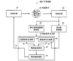
1.量子干渉装置
図1は、本実施形態の量子干渉装置の機能ブロック図である。本実施形態の量子干渉装置1は、光発生部10、金属原子20、光検出部30、制御信号生成部40、周波数制御部50、最大周波数偏移制御部60を含んで構成されている。
1. Quantum Interference Device FIG. 1 is a functional block diagram of the quantum interference device of the present embodiment. The
制御信号生成部40は、周波数変調された制御信号12を生成する。
The control signal generator 40 generates the frequency-modulated
光発生部10は、制御信号12の周波数に応じた周波数差の第1の光と第2の光を発生させる。
The
金属原子20は、Λ型3準位を有する金属原子であり、例えば、ナトリウム(Na)原子、ルビジウム(Rb)原子、セシウム(Cs)原子等のアルカリ金属原子である。 The metal atom 20 is a metal atom having a Λ-type three level, for example, an alkali metal atom such as a sodium (Na) atom, a rubidium (Rb) atom, or a cesium (Cs) atom.
光検出部30は、光発生部10から照射されて金属原子20を透過した光を検出する。
The
周波数制御部50は、光検出部30の検出信号に基づいて、第1の光と第2の光が共鳴光対(金属原子20に電磁誘起透過現象を発生させる共鳴光対)となるように制御信号12の周波数を制御する。
Based on the detection signal of the
最大周波数偏移制御部60は、光検出部30の検出信号に応じて、制御信号12の最大周波数偏移を制御する。最大周波数偏移制御部60は、例えば、制御信号12の周波数を一定にする、光検出部30の検出信号の強度と制御信号12の最大周波数偏移との対応関係の情報を記憶し、当該対応関係の情報に基づいて、制御信号12の最大周波数偏移を制御するようにしてもよい。
The maximum frequency
制御信号生成部40は、発振信号生成部42、変調信号生成部44、周波数変調部46、周波数変換部48を含むように構成してもよい。
The control signal generation unit 40 may include an oscillation
発振信号生成部42は、周波数制御部50の出力信号に応じた周波数の発振信号43を生成する。
The
変調信号生成部44は、所与の変調信号45を生成する。
The
周波数変調部46は、発振信号43を変調信号45で周波数変調する。
The
周波数変換部48は、周波数変調部46の出力信号の周波数を変換して制御信号12を生成する。
The
周波数制御部50は、例えば、変調信号45と同じ周波数の信号に基づいて、光検出部30の検出信号を検波するようにしてもよい。
For example, the
最大周波数偏移制御部60は、例えば、光検出部30の検出信号に基づいて、変調信号45の振幅を制御するようにしてもよい。最大周波数偏移制御部60は、例えば、制御信号12の周波数を一定にする、光検出部30の検出信号の強度と制御信号12の最大周波数偏移との対応関係に従って、変調信号42の振幅を制御するようにしてもよい。
For example, the maximum frequency
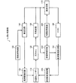
図2は、本実施形態の量子干渉装置の他の機能ブロック図である。図2に示すように、本実施形態の量子干渉装置1では、図1に示した量子干渉装置1に対して、最大周波数偏移情報変更部70が追加されている。
FIG. 2 is another functional block diagram of the quantum interference device of the present embodiment. As shown in FIG. 2, in the
最大周波数偏移情報変更部70は、量子干渉装置1の外部からの信号に基づいて、光検出部30の検出信号の強度と制御信号12の最大周波数偏移との対応関係の情報を変更する。
The maximum frequency deviation
図2のその他の各構成の機能は、図1と同様であるため同じ符号を付しており、その説明を書略する。 The functions of the other components in FIG. 2 are the same as those in FIG.
以下では、量子干渉装置1の一例として、原子発振器を例に挙げて詳細に説明する。
Hereinafter, an atomic oscillator will be described as an example of the
2.原子発振器
2−1.第1実施形態
図3は、第1実施形態の原子発振器の構成例を示す図である。図3に示すように、第1実施形態の原子発振器1は、半導体レーザー110、ガスセル120、光検出器130、検波回路140、電流駆動回路150、低周波発振器160、検波回路170、電圧制御水晶発振器(VCXO)180、周波数変調回路190、低周波発振器200、振幅制御回路210、周波数変換回路220を含んで構成されている。
2. Atomic oscillator 2-1. First Embodiment FIG. 3 is a diagram illustrating a configuration example of an atomic oscillator according to a first embodiment. As shown in FIG. 3, the
ガスセル120は、容器中に気体状のアルカリ金属原子が封入されたものである。
The
半導体レーザー110は、周波数の異なる複数の光を発生させてガスセル120に照射する。具体的には、電流駆動回路150が出力する駆動電流によって、半導体レーザー110の出射光の中心波長λ0(中心周波数はf0)が制御される。そして、半導体レーザー110は、周波数変換回路220の出力信号を変調信号として変調がかけられる。すなわち、電流駆動回路150による駆動電流に、周波数変換回路220の出力信号(変調信号)を重畳することにより、半導体レーザー110は変調がかかった光を発生させる。このような半導体レーザー110は、例えば、端面発光レーザー(Edge Emitting Laser)や、垂直共振器面発光レーザー(VCSEL:Vertical Cavity Surface Emitting Laser)等の面発光レーザーなどで実現することができる。
The
光検出器130は、ガスセル120を透過した光を検出し、光の強度に応じた検出信号を出力する。前述したように、周波数差が、アルカリ金属原子の2つの基底準位のエネルギー差ΔE12に相当する周波数と一致する2種類の光をアルカリ金属原子に照射すると、アルカリ金属原子はEIT現象を起こす。このEIT現象を起こすアルカリ金属原子の数が多いほどガスセル120を透過する光の強度が増大し、光検出器130の出力信号の電圧レベルが高くなる。
The
光検出器130の出力信号は検波回路140と検波回路170に入力される。検波回路140は、数Hz〜数百Hz程度の低い周波数で発振する低周波発振器160の発振信号を用いて光検出器130の出力信号を同期検波する。
The output signal of the
電流駆動回路150は、検波回路140の出力信号に応じた大きさの駆動電流を発生して半導体レーザー110に供給し、半導体レーザー110の出射光の中心波長λ0(中心周波数f0)を制御する。具体的には、アルカリ金属原子の2P3/2のI−1/2の励起準位(I+1/2の励起準位でもよい)と2S1/2のI−1/2の基底準位とのエネルギー差に相当する波長λ1(周波数f1)、アルカリ金属原子の2P3/2のI−1/2の励起準位(I+1/2の励起準位でもよい)と2S1/2のI+1/2の基底準位とのエネルギー差に相当する波長λ2(周波数f2)に対して、中心波長λ0が(λ1+λ2)/2に一致する(中心周波数f0が(f1+f2)/2に一致する)ように制御される。あるいは、アルカリ金属原子の2P1/2のI−1/2の励起準位(I+1/2の励起準位でもよい)と2S1/2のI−1/2の基底準位とのエネルギー差に相当する波長λ1(周波数f1)、アルカリ金属原子の2P1/2のI−1/2の励起準位(I+1/2の励起準位でもよい)と2S1/2のI+1/2の基底準位とのエネルギー差に相当する波長λ2(周波数f2)に対して、中心波長λ0が(λ1+λ2)/2に一致する(中心周波数f0が(f1+f2)/2に一致する)ように制御されるようにしてもよい。
The
ただし、いずれの場合も、中心波長λ0は必ずしも(λ1+λ2)/2と正確に一致させる必要はなく、(λ1+λ2)/2を中心とする所定範囲の波長であってもよい。なお、検波回路140による同期検波を可能とするために、電流駆動回路150が発生する駆動電流には低周波発振器160の発振信号(検波回路140に供給される発振信号と同じ信号)が重畳される。
However, in any case, the central wavelength lambda 0 is always (λ 1 + λ 2) / 2 exactly need not be matched, even wavelength in a predetermined range centered on (λ 1 + λ 2) / 2 Good. In order to enable synchronous detection by the
半導体レーザー110、ガスセル120、光検出器130、検波回路140、電流駆動回路150を通るフィードバックループにより、半導体レーザー110が発生させる光の中心波長λ0(中心周波数f0)が微調整される。
The center wavelength λ 0 (center frequency f 0 ) of the light generated by the
検波回路170は、数Hz〜数百Hz程度の低い周波数で発振する低周波発振器200の発振信号を用いて光検出器130の出力信号を同期検波する。そして、検波回路170の出力信号の大きさに応じて、電圧制御水晶発振器(VCXO)180の発振周波数が微調整される。電圧制御水晶発振器(VCXO)180は、例えば、数MHz〜数10MHz程度で発振する。
The
振幅制御回路210は、光検出器130の検出信号のレベルに応じて、低周波発振器200の発振信号の振幅を制御する。
The
周波数変調回路190は、検波回路170による同期検波を可能とするために、振幅制御回路210の出力信号(振幅が調整された低周波発振器200の発振信号)を変調信号として電圧制御水晶発振器(VCXO)180の出力信号を周波数変調(FM:Frequency Modulation)する。
In order to enable synchronous detection by the
周波数変換回路220は、一定の周波数変換率で周波数変調回路190の出力信号を周波数変換する。例えば、電圧制御水晶発振器(VCXO)180の発振周波数の中心値を10MHzとして、ガスセル120に封入されたアルカリ金属原子がセシウム原子であればΔE12に相当する周波数は9.192631770GHzなので、周波数変換率は(9.192631770GHz/10MHz)に設定される。周波数変換回路220は、例えば、PLL(Phase Locked Loop)回路により実現することができる。
The
このような構成の原子発振器1において、仮にEIT信号が左右対称であれば、半導体レーザー110、ガスセル120、光検出器130、検波回路170、電圧制御水晶発振器(VCXO)180、周波数変調回路190、周波数変換回路220を通るフィードバックループにより、周波数変換回路220の出力信号の周波数がΔE12に相当する周波数の1/2の周波数と正確に一致するように微調整される。例えば、アルカリ金属原子がセシウム原子であれば、ΔE12に相当する周波数が9.192631770GHzなので、周波数変換回路220の出力信号の周波数が4.596315885GHzと一致した状態で安定する。
In the
そして、前述したように、周波数変換回路220の出力信号が変調信号(変調周波数fm)となり、半導体レーザー110が共鳴光対を含む複数の光を発生させてガスセル120に照射する。
Then, as described above, the output signal of the
図4は、半導体レーザー110の出射光の周波数スペクトルを示す概略図である。図4において、横軸は光の周波数であり、縦軸は光の強度である。
FIG. 4 is a schematic diagram showing the frequency spectrum of the emitted light from the
図4に示すように、半導体レーザー110の出射光には、中心周波数f0(=v/λ0:vは光の速度、λ0は中心波長)を有する光と、その両側に変調周波数fmずつ周波数が異なる複数の光が含まれている。変調周波数fmはΔE12に相当する周波数の1/2に等しいので、周波数f1(=f0+fm)の光と周波数f2(=f0−fm)の光は、その差f1−f2(=2fm)がΔE12にほぼ等しく、ガスセル120に封入されたアルカリ金属原子にEIT現象を起こさせる共鳴光対となる。
As shown in FIG. 4, light emitted from the
なお、図3の半導体レーザー110、ガスセル120に含まれるアルカリ金属原子、光検出器130、検波回路170、振幅制御回路210は、それぞれ図1の光発生部10、金属原子20、光検出部30、周波数制御部50、最大周波数偏移制御部60に相当する。また、図3の電圧制御水晶発振器(VCXO)180、周波数変調回路190、低周波発振器200、周波数変換回路220による構成は、図1の制御信号生成部40に相当する。また、図3の電圧制御水晶発振器(VCXO)180、低周波発振器200、周波数変調回路190、周波数変換回路220は、それぞれ図1の発振信号生成部42、変調信号生成部44、周波数変調部46、周波数変換部48に相当する。
In addition, the alkali metal atom, the
次に、光検出器130の出力信号の同期検波の一例について詳細に説明する。
Next, an example of synchronous detection of the output signal of the
まず、振幅制御回路210が無いものとして考えると、周波数変調回路190は、低周波発振器200の発振信号を変調信号として電圧制御水晶発振器(VCXO)180の出力信号を周波数変調することになる。
First, assuming that the
図5(A)に示すように、低周波発振器200の発振信号は、周波数がfs(周期が1/fs)、振幅がAsの正弦波であり、周波数変調における最大周波数偏移(周波数デビエーション)Δfは、この振幅Asに比例する。図5(B)は、周波数変調回路190の出力信号の周波数スペクトラムを示す図であり、周波数変調回路190の出力信号は、低周波発振器200の発振周波数fVCXOを中心周波数として、その両側にfs間隔で複数の周波数成分を含む。そして、周波数変換回路220により周波数変調回路190の出力信号の周波数がN(=fm/fVCXO)倍されるので、周波数変換回路220の出力信号(半導体レーザー110の変調信号)は、厳密には、変調周波数fmを中心周波数として、その両側にfs×Nの間隔で複数の周波数成分を含む。
As shown in FIG. 5 (A), the oscillation signal of the low-
半導体レーザー110は、この周波数変換回路220の出力信号を変調信号として変調がかけられる。従って、半導体レーザー100の出射光には、厳密には、図4に示した各周波数成分の光とともに、その両側にfs×Nの間隔の複数の光も含まれる。このような複数の光がガスセル120に照射され、ガスセル120を透過した光が光検出器130で検出されるので、光検出器130の出力信号には直流成分とともに低周波数成分も含まれる。具体的には、図4に示した共鳴光対の周波数差f1−f2(=2fm)がΔE12に相当する周波数f12と正確に一致する場合、図6(A)に示すように、光検出器130の検出信号には、ピークの直流成分と一定振幅の周波数2fsの低周波数成分が含まれる。また、共鳴光対の周波数差f1−f2がΔE12に相当する周波数f12から少しだけずれた場合(f1−f2=f12−Δ1の場合)も、図6(B)に示すように、光検出器130の検出信号には、同様に、ピークの直流成分と周波数2fsの低周波数成分が含まれる。ただし、周波数2fsの低周波数成分の振幅は1周期毎に変化し、2周期(1/fs)毎に同じ振幅になる。
The
一方、共鳴光対の周波数差f1−f2がΔE12に相当する周波数f12からかなりずれた場合(f1−f2=f12−Δ2あるいはf1−f2=f12+Δ2の場合)、図7(A)や図7(B)に示すように、光検出器130の検出信号には、直流成分と周波数fsの低周波数成分が含まれる。
On the other hand, when the frequency difference f 1 -f 2 of the resonant light pair deviates considerably from the frequency f 12 corresponding to ΔE 12 (f 1 -f 2 = f 12 -Δ 2 or f 1 -f 2 = f 12 + Δ 2 In this case, as shown in FIGS. 7A and 7B, the detection signal of the
そこで、検波回路170は、例えば、図8に示すように構成することができる。すなわち、図8に示すように、光検出器130の出力信号と周波数発生源172が発生させる一定周波数fsの発振信号とをミキサー174で混合し、周波数fsが減衰域に含まれるローパスフィルター176を通して電圧制御水晶発振器(VCXO)180に出力する。検波回路170をこのような構成にすれば、ミキサー174の出力信号には、光検出器130の出力信号と周波数fsの発振信号との和信号と差信号が発生するので、光検出器130の出力信号に含まれる直流成分がミキサー174に入力されると、ミキサー174の出力には周波数fsの信号のみが発生するが、ローパスフィルター176で除去される。また、光検出器130の出力信号が、図6(A)のような周波数2fsの低周波成分を含む場合、この周波数2fsの低周波成分がミキサー174に入力されると、ミキサー174の出力には周波数3fsの信号と周波数fsの信号が発生するが、これらの信号もローパスフィルター176で除去される。つまり、光検出器130の出力信号が図6(A)のような場合、検波回路170の出力信号の電圧値は0(基準電圧値)となる。この検波回路170の出力信号が電圧制御水晶発振器(VCXO)180に入力されるため、電圧制御水晶発振器(VCXO)180の発振周波数は変化しない。
Therefore, the
これに対して、光検出器130の出力信号が、図6(B)のような周波数2fsの低周波成分を含む場合、この周波数2fsの低周波成分がミキサー174に入力されると、ミキサー174の出力には周波数3fsの信号と周波数fsの信号が発生するが、これらの信号はローパスフィルター176で除去される。ところが、この2fsの低周波成分は振幅が2周期(1/fs)毎に同じ振幅になるので、光検出器130の出力信号には、周波数fsの低周波成分もわずかに含まれる。この周波数fsの低周波成分がミキサー174に入力されると、ミキサー174の出力には周波数2fsの信号と正電圧の直流信号が発生する。周波数2fsの信号はローパスフィルター176で除去されるが、正電圧の直流信号は除去されずに残る。つまり、光検出器130の出力信号が図6(B)のような場合、検波回路170の出力信号の電圧値は正(基準電圧値よりも高い電圧値)となる。この検波回路170の出力信号が電圧制御水晶発振器(VCXO)180に入力されると、電圧制御水晶発振器(VCXO)180の発振周波数は高い方に変化する。
In contrast, the output signal of the
また、光検出器130の出力信号が、図7(A)のような周波数fsの低周波成分を含む場合、この周波数fsの低周波成分がミキサー174に入力されると、ミキサー174の出力には周波数2fsの信号と正電圧の直流信号が発生する。周波数2fsの信号はローパスフィルター176で除去されるが、正電圧の直流信号は除去されずに残る。つまり、光検出器130の出力信号が図7(A)のような場合、検波回路170の出力信号の電圧値は正(基準電圧値よりも高い電圧値)となる。この検波回路170の出力信号が電圧制御水晶発振器(VCXO)180に入力されると、電圧制御水晶発振器(VCXO)180の発振周波数は高い方に変化する。
In addition, when the output signal of the
同様に、光検出器130の出力信号が、図7(B)のような周波数fsの低周波成分を含む場合、この周波数fsの低周波成分がミキサー174に入力されると、ミキサー174の出力には周波数2fsの信号と負電圧の直流信号が発生する。周波数2fsの信号はローパスフィルター176で除去されるが、負電圧の直流信号は除去されずに残る。つまり、光検出器130の出力信号が図7(B)のような場合、検波回路170の出力信号の電圧値は負(基準電圧値よりも低い電圧値)となる。この検波回路170の出力信号が電圧制御水晶発振器(VCXO)180に入力されると、電圧制御水晶発振器(VCXO)180の発振周波数は低い方に変化する。
Similarly, when the output signal of the
このように、検波回路170の出力信号の電圧値に応じて、電圧制御水晶発振器(VCXO)180の発振周波数を変化させることで、共鳴光対の周波数差f1−f2がΔE12に相当する周波数f12と一致するように(周波数変換回路120の周波数fmがΔE12に相当する周波数f12の1/2の周波数と一致するように)、フィードバック制御することができる。ただし、図6(A),図6(B),図7(A),図7(B)では、ガスセル120の透過光のEIT信号が左右対称であることを前提としており、その結果、光検出器130の検出信号の強度も、共鳴光対の周波数差f1−f2=f12を中心として左右対称になっている。そのため、光検出器130の検出信号の強度がピークとなるようにフィードバック制御がかかり、共鳴光対の周波数差f1−f2がΔE12に相当する周波数f12と一致する状態で安定する。
Thus, the frequency difference f 1 -f 2 of the resonant light pair is equivalent to ΔE 12 by changing the oscillation frequency of the voltage controlled crystal oscillator (VCXO) 180 in accordance with the voltage value of the output signal of the
一方、EIT信号が左右非対称の場合、光検出器130の検出信号の強度も、共鳴光対の周波数差f1−f2=f12を中心として左右非対称になる。そのため、共鳴光対の周波数差f1−f2=f12である場合、図9(A)に示すように、光検出器130の検出信号に含まれる周波数2fsの低周波数成分の振幅は一定にならず、1周期毎に振幅が変化し、2周期(1/fs)毎に同じ振幅になる。従って、この周波数2fsの低周波成分が検波回路170に入力されると、図6(B)の場合と同様に、検波回路170の出力信号の電圧値は正(基準電圧値よりも高い電圧値)となる。この検波回路170の出力信号が電圧制御水晶発振器(VCXO)180に入力されると、電圧制御水晶発振器(VCXO)180の発振周波数は高い方に変化する。
On the other hand, when the EIT signal is asymmetrical, the intensity of the detection signal of the
これに対して、図9(B)に示すように、共鳴光対の周波数差f1−f2がf12から少しだけずれた状態(f1−f2=f12+Δ3)で、光検出器130の検出信号に含まれる周波数2fsの低周波数成分の振幅が一定になる。従って、この周波数2fsの低周波成分が検波回路170に入力されると、図6(A)の場合と同様に、検波回路170の出力信号の電圧値は0(基準電圧値)となる。この検波回路170の出力信号が電圧制御水晶発振器(VCXO)180に入力されるため、電圧制御水晶発振器(VCXO)180の発振周波数は変化しない。従って、f1−f2=f12+Δ3となるように(周波数変換回路120の周波数fm=(f12+Δ3)/2となるように)、フィードバック制御がかかる。
On the other hand, as shown in FIG. 9B, in the state where the frequency difference f 1 -f 2 of the resonant light pair is slightly shifted from f 12 (f 1 -f 2 = f 12 + Δ 3 ), the amplitude of the low frequency component of the
このように、EIT信号が左右非対称であれば、光検出器130の検出信号の強度も、共鳴光対の周波数差f1−f2=f12を中心として左右非対称になるので、光検出器130の検出信号の強度がピークから少しずれた値となるようにフィードバック制御がかかり、共鳴光対の周波数差f1−f2がΔE12に相当する周波数f12から少しずれた周波数と一致する状態で安定する。このような周波数がずれた状態でも高い周波数安定度を確保することはできる。
Thus, if the EIT signal is left-right asymmetric, the intensity of the detection signal of the
ところで、ガスセル120の温度が不安定になる等の要因でEIT信号のピーク値(強度)が変化し、これに応じてEIT信号の線幅が変化することが考えられる。例えば、図9(B)の状態(f1−f2=f12+Δ3)で電圧制御水晶発振器(VCXO)180の発振周波数が安定している場合に、EIT信号のピーク値(強度)が低下して図10のように線幅が広くなった場合、f1−f2=f12+Δ4の状態で、光検出器130の検出信号に含まれる周波数2fsの低周波数成分の振幅が一定になり、電圧制御水晶発振器(VCXO)180の発振周波数が安定する。図9(B)の例と図10の例を比較するとΔ4≠Δ3(Δ4>Δ3)であり、EIT信号のピーク値(強度)が低下すると電圧制御水晶発振器(VCXO)180の発振周波数が高い方向にシフトしている。従って、EIT信号が左右非対称の場合、EIT信号のピーク値(強度)が変化することで線幅が変化すると、周波数安定度が劣化する可能性がある。
By the way, it is conceivable that the peak value (intensity) of the EIT signal changes due to factors such as the temperature of the
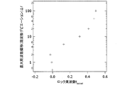
従って、EIT信号が左右非対称の場合、EIT信号のピーク値(強度)が変化することで線幅が変化しても、電圧制御水晶発振器(VCXO)180の発振周波数が変化しないように、何らかの対策を考える必要がある。そこで、左右非対称なEIT信号をモデル化し、EIT信号のピーク値(強度)を変化させて、電圧制御水晶発振器(VCXO)180が安定発振する時の周波数変換回路220の出力信号の周波数(ロック周波数flocked)の変化の様子をシミュレーションで確認した。図11は、左右非対称なEIT信号のモデルをグラフ化した図であり、図12は、シミュレーション結果を示す図である。図11の各軸の単位は任意単位であり、横軸は(f1−f2)−f12の値、縦軸はガスセル120の透過光の強度である。また、図12の各軸の単位は任意単位であり、横軸はEIT信号強度、縦軸はロック周波数flockedである。図12に示す4つのグラフG1,G2,G3,G4は、それぞれ、EIT信号強度の変化に伴うEIT信号の線幅変化の度合い(BF:Broadening Factor)が0,0.5,1.0,2.0のモデルに対するシミュレーション結果である。なお、BF=0は、EIT信号強度の変化に伴ってEIT信号の線幅変化が起きないモデルである。図12のシミュレーション結果によれば、ロック周波数flockedは、EIT信号強度の増加に対して線形に減少する。
Therefore, if the EIT signal is asymmetrical, some measure is taken so that the oscillation frequency of the voltage controlled crystal oscillator (VCXO) 180 does not change even if the line width changes due to the change of the peak value (intensity) of the EIT signal. Need to think about. Therefore, by modeling the asymmetric EIT signal and changing the peak value (intensity) of the EIT signal, the frequency (lock frequency) of the output signal of the
また、EIT信号が左右非対称の場合、低周波発振器200の発振信号の振幅As(周波数変調回路190の周波数変調における最大周波数偏移(周波数デビエーション)Δf)を変えると、上述した同期検波の原理より、検波回路170の出力信号に含まれる周波数fsあるいは2fsの信号波形が変化し、ロック周波数flockedが変化すると考えられる。そこで、図11に示した左右非対称なEIT信号のモデルに対して、EIT信号の強度は一定のまま、最大周波数偏移(周波数デビエーション)Δfを変化させて、ロック周波数flockedの変化の様子をシミュレーションで確認した。図13は、シミュレーション結果を示す図である。図13の各軸の単位は任意単位であり、横軸はロック周波数flocked、縦軸は最大周波数偏移(周波数デビエーション)Δfである。図13のシミュレーション結果によれば、ロック周波数flockedは、最大周波数偏移(周波数デビエーション)Δfの増加に対して単調増加する。
Also, if the EIT signal is asymmetrical, changing the low-oscillation
図12のシミュレーション結果と図13のシミュレーション結果より、EIT信号の強度が変化しても、その変化の程度に応じて、最大周波数偏移(周波数デビエーション)Δfを適切に変化させることで、ロック周波数flockedを一定に維持することができると考えられる。特に、EIT信号の非線形性の状態によっては、EIT信号の強度の変化に応じて、最大周波数偏移(周波数デビエーション)Δfを最適に変化させることで、ロック周波数flockedをf12/2からのずれがない状態(EIT信号のピークを検出する状態)で一定に維持することができる場合もあると考えられる。図14は、ロック周波数flockedをf12/2からのずれがない状態で一定に維持するための、最大周波数偏移(周波数デビエーション)ΔfとEIT信号強度との関係をシミュレーションにより求めた結果を示す図である。図14のシミュレーション結果によれば、最大周波数偏移(周波数デビエーション)Δfを、EIT信号強度の増加に対してほぼ線形に増加させることで、ロック周波数flockedを一定に維持することができる。 From the simulation results in FIG. 12 and the simulation results in FIG. 13, even if the intensity of the EIT signal changes, the maximum frequency deviation (frequency deviation) Δf is appropriately changed according to the degree of the change, thereby obtaining the lock frequency. It is considered that f locked can be kept constant. Especially, the non-linearity of the states of the EIT signal, in response to changes in the intensity of the EIT signal, the maximum frequency shift (frequency deviation) Delta] f a by causing optimally changed, the lock frequency f locked from f 12/2 It is considered that there may be a case where it can be kept constant in a state where there is no deviation (a state where the peak of the EIT signal is detected). 14, for maintaining the lock frequency f locked constant with no deviation from f 12/2, the maximum frequency shift the result obtained by simulating a relationship between the (frequency deviation) Delta] f and EIT signal strength FIG. According to the simulation result of FIG. 14, the lock frequency f locked can be kept constant by increasing the maximum frequency deviation (frequency deviation) Δf almost linearly with respect to the increase in EIT signal strength.
周波数変調回路190の周波数変調における最大周波数偏移(周波数デビエーション)Δfは、低周波発振器200の発振信号の振幅Asに比例するので、低周波発振器200の発振信号の振幅を変えることで、最大周波数偏移(周波数デビエーション)Δfを変えることができる。また、EIT信号強度の変化は、光検出器130の検出信号(直流成分)のレベルの変化として現れる。従って、光検出器130の検出信号のレベルに応じて、図14に示したような所定の対応関係に従って低周波発振器200の発振信号の振幅を変化させることで、ロック周波数flockedを一定に維持することができると考えられる。
Maximum frequency deviation (frequency deviation) Delta] f in the frequency modulation of the
そこで、本実施形態の原子発振器1では、振幅制御回路210を追加し、振幅制御回路210により、光検出器130の検出信号のレベルに応じて、所定の対応関係に従って低周波発振器200の発振信号の振幅を制御している。例えば、サンプル評価などで得られる実際のEIT信号に合致したモデルを作成して上述の各種シミュレーションを行い、EIT信号強度を変数として、多項式近似により、ロック周波数flockedを一定に維持するための最大周波数偏移(周波数デビエーション)Δfの式を求める。そして、振幅制御回路210は、この最大周波数偏移(周波数デビエーション)Δfの式に従うように、低周波発振器200の発振信号の振幅を制御する。
Therefore, in the
なお、振幅制御回路210は、光検出器130の検出信号のレベルに応じて可変利得増幅器の利得を変えることで低周波発振器200の発振信号の振幅を制御するようにしてもよいし、光検出器130の検出信号のレベルに応じて可変アッテネーターの減衰量を変えることで低周波発振器200の発振信号の振幅を制御するようにしてもよい。
The
このように、本実施形態の原子発振器によれば、振幅制御回路210を設けることで、EIT信号強度の変化によるロック周波数の変動分を、最大周波数偏移(周波数デビエーション)Δfの変化によるロック周波数の変動分で打ち消すことができるので、EIT信号強度が変化してもロック周波数を一定に保持することができる。従って、従来よりも高い周波数安定度の原子発振器を実現することができる。特に、ロック周波数flocked=f12/2に維持するような最大周波数偏移(周波数デビエーション)Δfの多項式が得られる場合は、従来よりも高い周波数精度と周波数安定度の原子発振器を実現することができる。
As described above, according to the atomic oscillator of the present embodiment, by providing the
2−2.第2実施形態
第1実施形態の原子発振器では、最大周波数偏移(周波数デビエーション)Δfの式が不変としていたが、製造条件のばらつき等に起因してサンプル間でEIT信号の特性が異なることが想定される。そこで、第2実施形態の原子発振器では、各サンプルのEIT信号の特性に応じて最大周波数偏移(周波数デビエーション)Δfの式を補正する。
2-2. Second Embodiment In the atomic oscillator of the first embodiment, the equation of the maximum frequency deviation (frequency deviation) Δf is unchanged, but the characteristics of the EIT signal may differ between samples due to variations in manufacturing conditions. is assumed. Therefore, in the atomic oscillator of the second embodiment, the equation of the maximum frequency deviation (frequency deviation) Δf is corrected according to the characteristics of the EIT signal of each sample.
図15は、第2実施形態の原子発振器の構成例を示す図である。図15に示すように、第2実施形態の原子発振器1では、図3に示した第1実施形態の原子発振器1に対して、補正回路230が追加されている。なお、第2実施形態におけるその他の構成は、第1実施形態と同じであるため同じ符号を付しており、その説明を省略する。
FIG. 15 is a diagram illustrating a configuration example of the atomic oscillator according to the second embodiment. As shown in FIG. 15, in the
補正回路230は、振幅制御回路210による低周波発振器200の発振信号の振幅制御に用いられる最大周波数偏移(周波数デビエーション)Δfの式を補正する。例えば、設計段階では、多項式近似により、最大周波数偏移(周波数デビエーション)Δfの式(多項式)を求めて、振幅制御回路210が当該多項式に従って低周波発振器200の発振信号の振幅を制御するように設計しておく。そして、各サンプルの検査時などに、実際のEIT信号の特性を評価し、最大周波数偏移(周波数デビエーション)Δfの正しい式を求める。補正回路230には、この最大周波数偏移(周波数デビエーション)Δfの正しい式の情報を記憶させ、振幅制御回路210は、最大周波数偏移(周波数デビエーション)Δfの正しい式に従って、低周波発振器200の発振信号の振幅を制御する。例えば、書き込みが可能な不揮発性のメモリーに、最大周波数偏移(周波数デビエーション)Δfの正しい式(多項式)の各係数値、あるいは最大周波数偏移(周波数デビエーション)Δfの正しい式(多項式)の各係数値と設計段階の式(多項式)の各係数値との差分を書き込むことで、補正回路230を構成することができる。前者の場合、振幅制御回路210は、不揮発性のメモリーに書き込まれた各係数値の多項式に従って、低周波発振器200の発振信号の振幅を制御する。後者の場合、振幅制御回路210は、不揮発性のメモリーに書き込まれた各係数値の差分から正しい係数値を求めて、当該正しい係数値の多項式に従って、低周波発振器200の発振信号の振幅を制御する。
The
第2実施形態におけるその他の構成は、第1実施形態と同じであるため同じ符号を付しており、その説明を省略する。 Since other configurations in the second embodiment are the same as those in the first embodiment, the same reference numerals are given, and descriptions thereof are omitted.
なお、図15の半導体レーザー110、ガスセル120に含まれるアルカリ金属原子、光検出器130、検波回路170は、それぞれ図1の光発生部10、金属原子20、光検出部30、周波数制御部50に相当する。また、図15の振幅制御回路210と補正回路230による構成は、図1の最大周波数偏移制御部60に相当する。また、図15の電圧制御水晶発振器(VCXO)180、周波数変調回路190、低周波発振器200、周波数変換回路220による構成は、図1の制御信号生成部40に相当する。また、図15の電圧制御水晶発振器(VCXO)180、低周波発振器200、周波数変調回路190、周波数変換回路220は、それぞれ図1の発振信号生成部42、変調信号生成部44、周波数変調部46、周波数変換部48に相当する。
In addition, the alkali metal atom, the
この第2実施形態の原子発振器によれば、サンプル毎に適切な最大周波数偏移(周波数デビエーション)Δfの式を不揮発性のメモリーに記憶させておくことで、サンプル間のEIT信号の特性ばらつきを吸収することができるので、サンプルに依存せずに高い周波数安定度を確保できる。 According to the atomic oscillator of the second embodiment, by storing an equation of an appropriate maximum frequency deviation (frequency deviation) Δf for each sample in a nonvolatile memory, the characteristic variation of the EIT signal between samples can be reduced. Since it can absorb, high frequency stability can be secured without depending on the sample.
2−3.第3実施形態
第2実施形態の原子発振器では、補正回路230を設けたことでサンプル間のEIT信号の特性ばらつき(初期ばらつき)を吸収することができる。しかし、経年変化により、EIT信号の特性が変わると、これに応じて最大周波数偏移(周波数デビエーション)Δfの正しい式も変わるので、第2実施形態の原子発振器では、時間の経過とともに、低周波発振器200の発振信号の振幅制御の精度が低下することが考えられる。そこで、第3実施形態の原子発振器では、最大周波数偏移(周波数デビエーション)Δfの式を書き換え可能に構成する。
2-3. Third Embodiment In the atomic oscillator of the second embodiment, by providing the
図16は、第3実施形態の原子発振器の構成例を示す図である。図16に示すように、第3実施形態の原子発振器1では、図15に示した第2実施形態の原子発振器1に対して、設定変更回路240が追加されている。
FIG. 16 is a diagram illustrating a configuration example of the atomic oscillator according to the third embodiment. As shown in FIG. 16, in the
設定変更回路240は、振幅制御回路210による低周波発振器200の発振信号の振幅制御に用いられる最大周波数偏移(周波数デビエーション)Δfの式(具体的には各係数値)を書き換える。例えば、補正回路230の不揮発性メモリーを外部から書き換え可能にするインターフェース回路として構成される。設定変更回路240は、例えば、外部からクロック信号とシリアルデータ信号が入力され、書き込みアドレス、書き込みデータ(各係数値)、書き込み信号などを生成して不揮発性メモリーに出力する。
The setting
第3実施形態におけるその他の構成は、第1実施形態及び第2実施形態と同じであるため同じ符号を付しており、その説明を省略する。 Other configurations in the third embodiment are the same as those in the first embodiment and the second embodiment, and thus are denoted by the same reference numerals, and description thereof is omitted.
なお、図16の半導体レーザー110、ガスセル120に含まれるアルカリ金属原子、光検出器130、検波回路170、設定変更回路240は、それぞれ図2の光発生部10、金属原子20、光検出部30、周波数制御部50、最大周波数偏移情報変更部70に相当する。また、図16の振幅制御回路210と補正回路230による構成は、図2の最大周波数偏移制御部60に相当する。また、図16の電圧制御水晶発振器(VCXO)180、周波数変調回路190、低周波発振器200、周波数変換回路220による構成は、図2の制御信号生成部40に相当する。また、図16の電圧制御水晶発振器(VCXO)180、低周波発振器200、周波数変調回路190、周波数変換回路220は、それぞれ図2の発振信号生成部42、変調信号生成部44、周波数変調部46、周波数変換部48に相当する。
In addition, the alkali metal atom, the
この第3実施形態の原子発振器によれば、経年変化によりEIT信号の特性が変わっても、あらためて最大周波数偏移(周波数デビエーション)Δfの式を求めて不揮発性メモリーに記憶されている情報を更新することで、長期間にわたって高い周波数安定度を維持することができる。例えば、メンテナンスの際にEIT信号の特性を評価して最大周波数偏移(周波数デビエーション)Δfの式の各係数値を求めて、不揮発性メモリーに記憶されている各係数値を更新すればよい。 According to the atomic oscillator of the third embodiment, even if the characteristics of the EIT signal change due to aging, the information stored in the non-volatile memory is updated by again obtaining the equation of the maximum frequency deviation Δf. By doing so, high frequency stability can be maintained over a long period of time. For example, the characteristics of the EIT signal may be evaluated during maintenance to obtain each coefficient value of the maximum frequency deviation (frequency deviation) Δf, and each coefficient value stored in the nonvolatile memory may be updated.
3.変形例
本発明は本実施形態に限定されず、本発明の要旨の範囲内で種々の変形実施が可能である。
3. The present invention is not limited to this embodiment, and various modifications can be made within the scope of the present invention.
3−1.変形例1
例えば、本実施形態の原子発振器1において、半導体レーザー110の中心波長λ0(中心周波数f0)が、ガスセル120に封入されたアルカリ金属原子の2P1/2のI−1/2の励起準位(I+1/2の励起準位でもよい)と2S1/2のI+1/2の基底準位とのエネルギー差に相当する波長λ2(周波数f2)にほぼ一致するように電流駆動回路150による駆動電流を制御するとともに、周波数変換回路220が変調回路190の出力信号をΔE12に相当する周波数に等しい周波数の信号に変換するように変形してもよい。あるいは、本実施形態の原子発振器1において、半導体レーザー110の中心波長λ0(中心周波数f0)が、ガスセル120に封入されたアルカリ金属原子の2P1/2のI−1/2の励起準位(I+1/2の励起準位でもよい)と2S1/2のI−1/2の基底準位とのエネルギー差に相当する波長λ1(周波数f1)にほぼ一致するように電流駆動回路150による駆動電流を制御するとともに、周波数変換回路220が変調回路190の出力信号をΔE12に相当する周波数に等しい周波数の信号に変換するように変形してもよい。前者のケースでは中心波長λ0がλ2に一致する(中心周波数f0がf2に一致する)ように制御され、後者のケースでは中心波長λ0がλ1に一致する(中心周波数f0がf1に一致する)ように制御される。
3-1.
For example, in the
図17(A)は、前者のケースの半導体レーザー110の出射光の周波数スペクトルを示す概略図であり、図17(B)は、後者のケースの半導体レーザー110の出射光の周波数スペクトルを示す概略図である。図17(A)及び図17(B)において、横軸は光の周波数であり、縦軸は光の強度である。図17(A)の場合は、f1とf0の差f1−f0がΔE12に相当する周波数にほぼ等しいので、周波数f1の光と中心周波数f0の光がガスセル120に封入されたアルカリ金属原子にEIT現象を起こさせる共鳴光対となる。一方、図17(B)の場合は、f0とf2の差f0−f2がΔE12に相当する周波数にほぼ等しいので、中心周波数f0の光と周波数f2の光がガスセル120に封入されたアルカリ金属原子にEIT現象を起こさせる共鳴光対となる。
FIG. 17A is a schematic diagram showing the frequency spectrum of the emitted light from the
3−2.変形例2
また、例えば、図18に示すように、図3に示した第1実施形態の原子発振器1を電気光学変調器(EOM:Electro-Optic Modulator)を用いた構成に変形してもよい。図18において、図1と同じ構成には同じ符号を付しており、その説明を省略する。
3-2.
Further, for example, as shown in FIG. 18, the
図18に示す原子発振器1では、半導体レーザー110は、周波数変換回路220の出力信号(変調信号)による変調がかけられず、単一周波数f0の光を発生させる。この周波数f0の光は、電気光学変調器(EOM)250に入射し、周波数変換回路220の出力信号(変調信号)によって変調がかけられる。その結果、図4と同様の周波数スペクトルを有する光を発生させることができる。図18の原子発振器1では、半導体レーザー110と電気光学変調器(EOM)250による構成が図1の光発生部10に相当する。
In the
なお、電気光学変調器(EOM)250の代わりに、音響光学変調器(AOM:Acousto-Optic Modulator)を用いてもよい。 Note that an acousto-optic modulator (AOM) may be used instead of the electro-optic modulator (EOM) 250.
同様に、第2実施形態や第3実施形態の原子発振器を電気光学変調器(EOM)や音響光学変調器(AOM)を用いた構成に変形してもよい。 Similarly, the atomic oscillator of the second embodiment or the third embodiment may be modified to a configuration using an electro-optic modulator (EOM) or an acousto-optic modulator (AOM).
なお、本実施形態及び本変形例では原子発振器を例に挙げて説明したが、本発明は、原子発振器に限らず、共鳴光対によって金属原子に電磁誘起透過現象を発生させる様々な量子干渉装置に適用することができる。 In the present embodiment and this modification, the atomic oscillator has been described as an example. However, the present invention is not limited to the atomic oscillator, and various quantum interference devices that generate an electromagnetically induced transmission phenomenon in a metal atom by using a resonant light pair. Can be applied to.
例えば、本実施形態又は変形例の原子発振器と同様の構成により、ガスセル120の周辺の磁場の変化に追従して電圧制御水晶発振器(VCXO)180の発振周波数が変化するため、ガスセル120の近傍に磁気測定対象物を配置することで磁気センサーとして機能する量子干渉装置を実現することもできる。
For example, since the oscillation frequency of the voltage controlled crystal oscillator (VCXO) 180 changes following the change in the magnetic field around the
また、例えば、本実施形態又は変形例の原子発振器と同様の構成により、極めて安定した金属原子の量子干渉状態(量子コヒーレンス状態)を作り出すことができるので、ガスセル120に入射する共鳴光対を取り出すことで、量子コンピュータ等に用いる光源として機能する量子干渉装置を実現することもできる。
In addition, for example, an extremely stable quantum interference state (quantum coherence state) of a metal atom can be created by the same configuration as the atomic oscillator of this embodiment or the modification, and thus the resonant light pair incident on the
また、例えば、本実施形態又は変形例の原子発振器と同様の構成により、半導体レーザー110とガスセル120の間の空間に微粒子が存在すると共鳴光対の可干渉性が低下してEIT信号の強度が低下するため、EIT信号のプロファイルを解析することで、微粒子センサーとして機能する量子干渉装置を実現することもできる。
Further, for example, with the same configuration as the atomic oscillator of this embodiment or the modification, if fine particles exist in the space between the
本発明は、実施の形態で説明した構成と実質的に同一の構成(例えば、機能、方法及び結果が同一の構成、あるいは目的及び効果が同一の構成)を含む。また、本発明は、実施の形態で説明した構成の本質的でない部分を置き換えた構成を含む。また、本発明は、実施の形態で説明した構成と同一の作用効果を奏する構成又は同一の目的を達成することができる構成を含む。また、本発明は、実施の形態で説明した構成に公知技術を付加した構成を含む。 The present invention includes configurations that are substantially the same as the configurations described in the embodiments (for example, configurations that have the same functions, methods, and results, or configurations that have the same objects and effects). In addition, the invention includes a configuration in which a non-essential part of the configuration described in the embodiment is replaced. In addition, the present invention includes a configuration that exhibits the same operational effects as the configuration described in the embodiment or a configuration that can achieve the same object. Further, the invention includes a configuration in which a known technique is added to the configuration described in the embodiment.
1 量子干渉装置、1a 原子発振器、10 光発生部、12 制御信号、20 金属原子、30 光検出部、40 制御信号生成部、42 発振信号生成部、43 発振信号、44 変調信号生成部、45 変調信号、46 周波数変調部、48 周波数変換部、50 周波数制御部、60 最大周波数偏移制御部、70 最大周波数偏移情報変更部、110 半導体レーザー、120 ガスセル、130 光検出器、140 検波回路、150 電流駆動回路、160 低周波発振器、170 検波回路、172 周波数発生源、174 ミキサー、176 ローパスフィルター、180 電圧制御水晶発振器(VCXO)、190 周波数変調回路、200 低周波発振器、210 振幅制御回路、220 周波数変換回路、230 補正回路、240 設定変更回路、250 電気光学変調器(EOM)
DESCRIPTION OF
Claims (7)
前記制御信号の周波数に応じ、所定の周波数差を有する第1の光と第2の光とを発生させる光発生部と、
前記第1の光と前記第2の光とが照射される金属原子と、
前記金属原子を透過した光を検出する光検出部と、
前記光検出部の検出信号に基づいて、前記制御信号生成部を制御する周波数制御部と、
前記光検出部の検出信号のレベルに応じて、前記制御信号の最大周波数偏移を変化させるように前記制御信号生成部を制御する最大周波数偏移制御部と、
を有し、
前記第1の光と前記第2の光とが共鳴光対となるような周波数を有する前記制御信号を前記制御信号生成部が生成できるように、当該制御信号生成部を前記周波数制御部と前記最大周波数偏移制御部とで制御する、原子発振器。 A control signal generator for generating a frequency-modulated control signal;
A light generating unit that generates a first light and a second light having a predetermined frequency difference according to a frequency of the control signal;
Metal atoms irradiated with the first light and the second light;
A light detection unit for detecting light transmitted through the metal atom;
A frequency control unit for controlling the control signal generation unit based on a detection signal of the light detection unit;
A maximum frequency deviation control unit that controls the control signal generation unit to change the maximum frequency deviation of the control signal according to the level of the detection signal of the light detection unit;
I have a,
The control signal generation unit and the frequency control unit are configured so that the control signal generation unit can generate the control signal having a frequency such that the first light and the second light form a resonant light pair. An atomic oscillator controlled by the maximum frequency shift controller .
前記周波数制御部の出力信号に応じた周波数の発振信号を生成する発振信号生成部と、
変調信号を生成する変調信号生成部と、
前記発振信号を前記変調信号で周波数変調する周波数変調部と、
前記周波数変調部の出力信号の周波数を変換して前記制御信号を生成する周波数変換部と、を有し、
前記周波数制御部は、
前記変調信号と同じ周波数の信号に基づいて、前記光検出部の検出信号を検波し、
最大周波数偏移制御部は、
前記光検出部の検出信号のレベルに応じて前記変調信号の振幅を変化させることにより、前記最大周波数偏移を変化させる、請求項1に記載の原子発振器。 The control signal generator is
An oscillation signal generation unit that generates an oscillation signal having a frequency according to an output signal of the frequency control unit;
A modulation signal generator for generating a modulation signal;
A frequency modulation unit for frequency-modulating the oscillation signal with the modulation signal;
A frequency conversion unit that converts the frequency of the output signal of the frequency modulation unit to generate the control signal,
The frequency control unit
Based on a signal having the same frequency as the modulation signal, the detection signal of the light detection unit is detected,
The maximum frequency deviation control unit is
The atomic oscillator according to claim 1 , wherein the maximum frequency shift is changed by changing an amplitude of the modulation signal according to a level of a detection signal of the light detection unit.
前記制御信号の周波数を一定にする、前記光検出部の検出信号の強度と前記制御信号の最大周波数偏移との対応関係に従って、前記変調信号の振幅を変化させる請求項2に記載
の原子発振器。 The maximum frequency deviation control unit is
The atomic oscillator according to claim 2, wherein the amplitude of the modulation signal is changed according to a correspondence relationship between the intensity of the detection signal of the light detection unit and the maximum frequency shift of the control signal, which makes the frequency of the control signal constant. .
前記制御信号の周波数を一定にする、前記光検出部の検出信号の強度と前記制御信号の最大周波数偏移との対応関係の情報を記憶し、当該対応関係の情報に基づいて、前記制御信号の最大周波数偏移を変化させる、請求項1又は2に記載の原子発振器。 The maximum frequency deviation control unit is
Information on the correspondence relationship between the intensity of the detection signal of the light detection unit and the maximum frequency shift of the control signal that makes the frequency of the control signal constant is stored, and based on the information on the correspondence relationship, the control signal The atomic oscillator according to claim 1, wherein the maximum frequency shift of the is changed .
前記制御信号の周波数に応じ、所定の周波数差を有する第1の光と第2の光を発生させる光発生ステップと、
前記第1の光と前記第2の光を金属原子に照射する光照射ステップと、
前記金属原子を透過した光を検出する光検出ステップと、
前記光検出ステップで得られた検出信号に基づいて、前記制御信号生成ステップを制御する周波数制御ステップと、
前記光検出ステップで得られた検出信号のレベルに応じて、前記制御信号の最大周波数偏移を変化させるように前記制御信号生成ステップを制御する最大周波数偏移制御ステップと、
を含み、
前記第1の光と前記第2の光とが共鳴光対となるような周波数を有する前記制御信号を前記制御信号生成ステップで生成できるように、当該制御信号生成ステップを前記周波数制御ステップと前記最大周波数偏移制御ステップとで制御する、原子発振器の制御方法。 A control signal generating step for generating a frequency-modulated control signal;
A light generating step for generating a first light and a second light having a predetermined frequency difference according to a frequency of the control signal;
A light irradiation step of irradiating a metal atom with the first light and the second light;
A light detection step of detecting light transmitted through the metal atom;
A frequency control step for controlling the control signal generation step based on the detection signal obtained in the light detection step;
A maximum frequency deviation control step for controlling the control signal generation step to change the maximum frequency deviation of the control signal according to the level of the detection signal obtained in the light detection step;
Only including,
The control signal generation step is the frequency control step and the frequency control step so that the control signal having a frequency at which the first light and the second light form a resonant light pair can be generated in the control signal generation step. A method for controlling an atomic oscillator controlled by a maximum frequency shift control step .
前記制御信号の周波数に応じ、所定の周波数差を有する第1の光と第2の光を発生させる光発生部と、
前記第1の光と前記第2の光が照射される金属原子と、
前記金属原子を透過した光を検出する光検出部と、
前記光検出部の検出信号に基づいて、前記制御信号生成部を制御する周波数制御部と、
前記光検出部の検出信号のレベルに応じて、前記制御信号の最大周波数偏移を変化させるように前記制御信号生成部を制御する最大周波数偏移制御部と、を有し、
前記第1の光と前記第2の光とが共鳴光対となるような周波数を有する前記制御信号を前記制御信号生成部が生成できるように、当該制御信号生成部を前記周波数制御部と前記最大周波数偏移制御部とで制御する、量子干渉装置。 A control signal generator for generating a frequency-modulated control signal;
A light generating unit that generates a first light and a second light having a predetermined frequency difference according to a frequency of the control signal;
Metal atoms irradiated with the first light and the second light;
A light detection unit for detecting light transmitted through the metal atom;
A frequency control unit for controlling the control signal generation unit based on a detection signal of the light detection unit;
Depending on the level of the detection signal of the photo detecting portion, have a, the maximum frequency deviation control unit for controlling said control signal generator to vary the maximum frequency deviation of the control signal,
The control signal generation unit and the frequency control unit are configured so that the control signal generation unit can generate the control signal having a frequency such that the first light and the second light form a resonant light pair. A quantum interference device controlled by the maximum frequency shift control unit .
Priority Applications (3)
| Application Number | Priority Date | Filing Date | Title |
|---|---|---|---|
| JP2011269998A JP5818000B2 (en) | 2011-12-09 | 2011-12-09 | Atomic oscillator, control method of atomic oscillator, and quantum interference device |
| CN201210520867.0A CN103166636B (en) | 2011-12-09 | 2012-12-06 | Atomic oscillator, the control method of quantum interference device and quantum interference device |
| US13/707,905 US8860515B2 (en) | 2011-12-09 | 2012-12-07 | Atomic oscillator, control method of atomic oscillator and quantum interference apparatus |
Applications Claiming Priority (1)
| Application Number | Priority Date | Filing Date | Title |
|---|---|---|---|
| JP2011269998A JP5818000B2 (en) | 2011-12-09 | 2011-12-09 | Atomic oscillator, control method of atomic oscillator, and quantum interference device |
Publications (3)
| Publication Number | Publication Date |
|---|---|
| JP2013123091A JP2013123091A (en) | 2013-06-20 |
| JP2013123091A5 JP2013123091A5 (en) | 2015-01-22 |
| JP5818000B2 true JP5818000B2 (en) | 2015-11-18 |
Family
ID=48571442
Family Applications (1)
| Application Number | Title | Priority Date | Filing Date |
|---|---|---|---|
| JP2011269998A Expired - Fee Related JP5818000B2 (en) | 2011-12-09 | 2011-12-09 | Atomic oscillator, control method of atomic oscillator, and quantum interference device |
Country Status (3)
| Country | Link |
|---|---|
| US (1) | US8860515B2 (en) |
| JP (1) | JP5818000B2 (en) |
| CN (1) | CN103166636B (en) |
Cited By (1)
| Publication number | Priority date | Publication date | Assignee | Title |
|---|---|---|---|---|
| JP7005891B2 (en) | 2016-10-17 | 2022-01-24 | スターライト工業株式会社 | Double piping |
Families Citing this family (11)
| Publication number | Priority date | Publication date | Assignee | Title |
|---|---|---|---|---|
| US8237514B2 (en) * | 2009-02-06 | 2012-08-07 | Seiko Epson Corporation | Quantum interference device, atomic oscillator, and magnetic sensor |
| JP6537252B2 (en) * | 2014-11-14 | 2019-07-03 | シスメックス株式会社 | Sample measurement device |
| JP6519169B2 (en) * | 2014-12-19 | 2019-05-29 | セイコーエプソン株式会社 | Atomic resonance transition device, atomic oscillator, clock, electronic device and moving body |
| CN104503077B (en) * | 2014-12-24 | 2016-07-27 | 中国科学院上海高等研究院 | A kind of Opto-electronic system realizing quantum coherent |
| US10504033B1 (en) | 2018-11-13 | 2019-12-10 | Atom Computing Inc. | Scalable neutral atom based quantum computing |
| US11995512B2 (en) | 2018-11-13 | 2024-05-28 | Atom Computing Inc. | Scalable neutral atom based quantum computing |
| US11580435B2 (en) | 2018-11-13 | 2023-02-14 | Atom Computing Inc. | Scalable neutral atom based quantum computing |
| CN110488265B (en) * | 2019-07-08 | 2022-11-18 | 清远市天之衡传感科技有限公司 | Radar speed measurement system and method based on Reedberg atom electromagnetic induction transparency effect |
| CN110401104B (en) * | 2019-07-29 | 2020-10-16 | 中国科学院大学 | Frequency locking system and method based on transparent electromagnetic induction signals of Reidberg |
| EP4115352A4 (en) | 2020-03-02 | 2024-04-24 | Atom Computing Inc | Scalable neutral atom based quantum computing |
| US11875227B2 (en) | 2022-05-19 | 2024-01-16 | Atom Computing Inc. | Devices and methods for forming optical traps for scalable trapped atom computing |
Family Cites Families (17)
| Publication number | Priority date | Publication date | Assignee | Title |
|---|---|---|---|---|
| US6320472B1 (en) | 1999-01-26 | 2001-11-20 | Kernco, Inc. | Atomic frequency standard |
| US6265945B1 (en) | 1999-10-25 | 2001-07-24 | Kernco, Inc. | Atomic frequency standard based upon coherent population trapping |
| US6359916B1 (en) | 2000-06-05 | 2002-03-19 | Agilent Technologies, Inc. | Coherent population trapping-based frequency standard and method for generating a frequency standard incorporating a quantum absorber that generates the CPT state with high frequency |
| JP2002344314A (en) | 2001-05-21 | 2002-11-29 | Nec Miyagi Ltd | Rubidium atomic oscillator |
| US6806784B2 (en) | 2001-07-09 | 2004-10-19 | The National Institute Of Standards And Technology | Miniature frequency standard based on all-optical excitation and a micro-machined containment vessel |
| JP3755001B2 (en) | 2002-08-30 | 2006-03-15 | 独立行政法人情報通信研究機構 | Atomic oscillation acquisition device and atomic clock |
| US7778293B2 (en) * | 2003-06-19 | 2010-08-17 | Kernco Inc. | Determining and setting the frequency modulation index of a laser in a CPT frequency standard |
| US7345553B2 (en) * | 2004-03-18 | 2008-03-18 | Agilent Technologies, Inc. | Method and apparatus for reducing errors due to line asymmetry in devices utilizing coherent population trapping |
| CN100542038C (en) * | 2007-05-17 | 2009-09-16 | 江汉大学 | Passive Rb atom frequency standard locking indication and method for diagnosing faults |
| JP2009141048A (en) | 2007-12-05 | 2009-06-25 | Epson Toyocom Corp | Optical system and atomic oscillator |
| US8237514B2 (en) * | 2009-02-06 | 2012-08-07 | Seiko Epson Corporation | Quantum interference device, atomic oscillator, and magnetic sensor |
| JP5381400B2 (en) | 2009-02-06 | 2014-01-08 | セイコーエプソン株式会社 | Quantum interferometers, atomic oscillators, and magnetic sensors |
| CN101488753B (en) * | 2009-02-17 | 2011-07-27 | 北京大学 | Atomic clock reference frequency obtaining method and atomic clock |
| JP5369803B2 (en) * | 2009-03-23 | 2013-12-18 | セイコーエプソン株式会社 | Quantum interference device and atomic oscillator |
| JP2010226424A (en) | 2009-03-24 | 2010-10-07 | Seiko Epson Corp | Optical system and atomic oscillator |
| JP5540619B2 (en) | 2009-09-16 | 2014-07-02 | セイコーエプソン株式会社 | Control method of atomic oscillator |
| JP2011091476A (en) | 2009-10-20 | 2011-05-06 | Seiko Epson Corp | Atomic oscillator |
-
2011
- 2011-12-09 JP JP2011269998A patent/JP5818000B2/en not_active Expired - Fee Related
-
2012
- 2012-12-06 CN CN201210520867.0A patent/CN103166636B/en not_active Expired - Fee Related
- 2012-12-07 US US13/707,905 patent/US8860515B2/en not_active Expired - Fee Related
Cited By (1)
| Publication number | Priority date | Publication date | Assignee | Title |
|---|---|---|---|---|
| JP7005891B2 (en) | 2016-10-17 | 2022-01-24 | スターライト工業株式会社 | Double piping |
Also Published As
| Publication number | Publication date |
|---|---|
| CN103166636B (en) | 2016-08-03 |
| US8860515B2 (en) | 2014-10-14 |
| US20130147565A1 (en) | 2013-06-13 |
| CN103166636A (en) | 2013-06-19 |
| JP2013123091A (en) | 2013-06-20 |
Similar Documents
| Publication | Publication Date | Title |
|---|---|---|
| JP5818000B2 (en) | Atomic oscillator, control method of atomic oscillator, and quantum interference device | |
| JP5429469B2 (en) | Quantum interference device, atomic oscillator and magnetic sensor | |
| JP5589166B2 (en) | Atomic oscillator | |
| JP5892320B2 (en) | Optical module and atomic oscillator for an atomic oscillator | |
| JP5910807B2 (en) | Optical module and atomic oscillator for an atomic oscillator | |
| US11271575B2 (en) | Resonance generation method and atomic oscillator | |
| JP5609130B2 (en) | Atomic oscillator | |
| JP6511298B2 (en) | CPT resonance generation method, CPT resonance detection method, CPT resonance generator, atomic oscillator, magnetic sensor | |
| JP6056118B2 (en) | Optical module and atomic oscillator | |
| JP5679099B2 (en) | Atomic oscillator | |
| JP6142989B2 (en) | Quantum interference device, atomic oscillator, magnetic sensor, and method of manufacturing quantum interference device | |
| JP2015057841A (en) | Quantum interference device | |
| JP2010232792A (en) | Atomic oscillator | |
| US20230030450A1 (en) | Quantum interference apparatus, atomic oscillator, and control method | |
| JP5988023B2 (en) | Atomic oscillator control method and atomic oscillator | |
| JP2012049230A (en) | Quantum interference device and method of quantum interference | |
| JP2012019261A (en) | Atomic oscillator | |
| JP5880807B2 (en) | Coherent light source | |
| JP2017011680A (en) | Atomic oscillator | |
| JP5950097B2 (en) | Quantum interference device, atomic oscillator, electronic device, and quantum interference method | |
| JP2010199779A (en) | Atomic oscillator | |
| JP2014007760A (en) | Atomic oscillator |
Legal Events
| Date | Code | Title | Description |
|---|---|---|---|
| RD07 | Notification of extinguishment of power of attorney |
Free format text: JAPANESE INTERMEDIATE CODE: A7427 Effective date: 20140619 |
|
| A521 | Request for written amendment filed |
Free format text: JAPANESE INTERMEDIATE CODE: A523 Effective date: 20141202 |
|
| A621 | Written request for application examination |
Free format text: JAPANESE INTERMEDIATE CODE: A621 Effective date: 20141202 |
|
| A977 | Report on retrieval |
Free format text: JAPANESE INTERMEDIATE CODE: A971007 Effective date: 20150611 |
|
| A131 | Notification of reasons for refusal |
Free format text: JAPANESE INTERMEDIATE CODE: A131 Effective date: 20150617 |
|
| A521 | Request for written amendment filed |
Free format text: JAPANESE INTERMEDIATE CODE: A523 Effective date: 20150807 |
|
| TRDD | Decision of grant or rejection written | ||
| A01 | Written decision to grant a patent or to grant a registration (utility model) |
Free format text: JAPANESE INTERMEDIATE CODE: A01 Effective date: 20150902 |
|
| A61 | First payment of annual fees (during grant procedure) |
Free format text: JAPANESE INTERMEDIATE CODE: A61 Effective date: 20150915 |
|
| R150 | Certificate of patent or registration of utility model |
Ref document number: 5818000 Country of ref document: JP Free format text: JAPANESE INTERMEDIATE CODE: R150 |
|
| S531 | Written request for registration of change of domicile |
Free format text: JAPANESE INTERMEDIATE CODE: R313531 |
|
| R350 | Written notification of registration of transfer |
Free format text: JAPANESE INTERMEDIATE CODE: R350 |
|
| LAPS | Cancellation because of no payment of annual fees |