JP5381400B2 - Quantum interferometers, atomic oscillators, and magnetic sensors - Google Patents
Quantum interferometers, atomic oscillators, and magnetic sensors Download PDFInfo
- Publication number
- JP5381400B2 JP5381400B2 JP2009153402A JP2009153402A JP5381400B2 JP 5381400 B2 JP5381400 B2 JP 5381400B2 JP 2009153402 A JP2009153402 A JP 2009153402A JP 2009153402 A JP2009153402 A JP 2009153402A JP 5381400 B2 JP5381400 B2 JP 5381400B2
- Authority
- JP
- Japan
- Prior art keywords
- light
- frequency
- resonant
- quantum interference
- interference device
- Prior art date
- Legal status (The legal status is an assumption and is not a legal conclusion. Google has not performed a legal analysis and makes no representation as to the accuracy of the status listed.)
- Active
Links
Images


Description
本発明は、量子干渉装置、原子発振器、および磁気センサーに関し、さらに詳しくは、
EIT現象を効率良く発生させるための技術に関するものである。
The present invention relates to a quantum interference device, an atomic oscillator, and a magnetic sensor.
The present invention relates to a technique for efficiently generating an EIT phenomenon.
電磁誘起透過方式(EIT方式、CPT方式と呼ばれることもある)による原子発振器
は、アルカリ金属原子に波長の異なる二つの共鳴光を同時に照射すると、二つの共鳴光の
吸収が停止する現象(EIT現象)を利用した発振器である。図12(a)は一つのアル
カリ金属原子のエネルギー状態を示したものである。第1基底準位23と励起準位21と
のエネルギー差に相当する波長を有する第1共鳴光、あるいは第2基底準位24と励起準
位21とのエネルギー差に相当する波長を有する第2共鳴光を、それぞれ単独でアルカリ
金属原子に照射すると、良く知られているように光吸収が起きる。ところが、このアルカ
リ金属原子に第1共鳴光と第2共鳴光を同時に照射し、同時に照射される第1共鳴光と第
2共鳴光の周波数差が正確に第1基底準位23と第2基底準位24のエネルギー差(ΔE
12)に一致すると、図12(a)の系は2つの基底準位の重ね合わせ状態、即ち量子干
渉状態になり、励起準位21への励起が停止し透明化(EIT)現象が起きる。この現象
を利用し、第1共鳴光と第2共鳴光との波長差がΔE12からずれた時の光吸収挙動の急
峻な変化を検出、制御することで、高精度な発振器をつくることができる。また、ΔE1
2は外部磁気の強さやゆらぎで敏感に変化するので、EIT現象を利用して高感度な磁気
センサーをつくることもできる。
An atomic oscillator using an electromagnetically induced transmission method (sometimes called an EIT method or a CPT method) stops absorption of two resonance lights when an alkali metal atom is simultaneously irradiated with two resonance lights having different wavelengths (EIT phenomenon). ). FIG. 12 (a) shows the energy state of one alkali metal atom. The first resonant light having a wavelength corresponding to the energy difference between the
In accordance with 12), the system of FIG. 12A enters a superposition state of two ground levels, that is, a quantum interference state, and excitation to the
Since 2 changes sensitively due to the strength and fluctuation of external magnetism, it is possible to make a highly sensitive magnetic sensor using the EIT phenomenon.
ところで、EIT現象による光出力信号のSN比を向上させるには、共鳴光と相互作用
するアルカリ金属の原子数を増やしてやればよい。例えば、特許文献1では、原子発振器
の出力信号のSN比を良くすることを目的として、気体状のアルカリ金属原子を閉じ込め
たセルの厚みを大きくしたり、或いはセルに入射するレーザー光のビーム径を大きくする
といった方法が開示されている。いずれの方法も、アルカリ金属原子が共鳴光に接触する
領域を広くするために、図12(b)或いは図12(c)のようにセルの厚みか高さを大
きくしている。ここで使用されているレーザー光については、EIT現象の発現条件を満
たす2種類の波長のレーザー光を一対のみ用いている。
By the way, in order to improve the S / N ratio of the optical output signal due to the EIT phenomenon, the number of alkali metal atoms interacting with the resonant light may be increased. For example, in
セル内の気体状のアルカリ金属原子の集団を構成する個々の原子に着目すると、それぞ
れの運動状態に応じた一定の速度分布を持っている。この原子集団に対して入射されるレ
ーザー光の波長が2種類(一対)のみだと、原子の運動によるドップラー効果(ドップラ
ーシフト)の影響で、実際に相互作用できるのは、セル内の多数の原子の内、レーザー入
射方向に対する特定の速度成分の値を持ったごく一部の原子に限られてしまい、EIT発
現に寄与する原子の割合が極めて低い。特許文献1に開示されている従来技術は、このよ
うなEIT発現効率が低い状態で構成された原子発振器であるので、信号対雑音比(S/
N比)の大きい所望の吸収スペクトルを得るには、セルの厚みか或いは高さの何れかを大
きくしなければならず、信号対雑音比を維持しながら小型化することは困難であるという
課題があった。つまり、セル内の単位体積あたりでEIT現象に寄与する原子数に変わり
はないままである。本発明は、かかる課題に鑑みてなされたものであり、波長が異なる複
数の共鳴光対を生成することにより、セル内のより多くの気体状のアルカリ金属原子に対
してEIT現象を効率よく発生させる量子干渉装置を提供し、これを利用することで小型
の原子発振器、あるいは磁気センサーを提供することを目的とする。
When attention is paid to individual atoms constituting a group of gaseous alkali metal atoms in the cell, it has a constant velocity distribution corresponding to each motion state. If there are only two types (one pair) of wavelengths of laser light incident on this atomic group, the interaction with the Doppler effect (Doppler shift) due to the movement of the atoms can actually interact. Among the atoms, only a few atoms having a specific velocity component value with respect to the laser incident direction are limited, and the proportion of atoms contributing to EIT expression is extremely low. Since the prior art disclosed in
In order to obtain a desired absorption spectrum having a large (N ratio), either the thickness or height of the cell must be increased, and it is difficult to reduce the size while maintaining the signal-to-noise ratio. was there. That is, the number of atoms contributing to the EIT phenomenon per unit volume in the cell remains unchanged. The present invention has been made in view of such problems, and by generating a plurality of resonant light pairs having different wavelengths, the EIT phenomenon is efficiently generated for more gaseous alkali metal atoms in the cell. It is an object of the present invention to provide a quantum interference device to be used, and to provide a small atomic oscillator or a magnetic sensor by using the quantum interference device.
本発明は、上述の課題の少なくとも一部を解決するためになされたものであり、以下の
形態又は適用例として実現することが可能である。
SUMMARY An advantage of some aspects of the invention is to solve at least a part of the problems described above, and the invention can be implemented as the following forms or application examples.
[適用例1]本発明の量子干渉装置は、エネルギー準位が異なる2つの基底準位を持った気体状のアルカリ金属原子に中心周波数が異なる複数の共鳴光対を入射し、前記複数の共鳴光対の前記中心周波数同士間の周波数差が前記アルカリ金属原子の速度分散に対応したドップラー幅よりも小さく、かつ、前記共鳴光対をなす2つの共鳴光の周波数差に基づくエネルギー差が前記2つの基底準位間のエネルギー差と一致しており、前記アルカリ金属原子に電磁誘起透過現象を発生させることを特徴とする。 Application Example 1 In the quantum interference device of the present invention, a plurality of resonant light pairs having different center frequencies are incident on a gaseous alkali metal atom having two ground levels having different energy levels, and the plurality of resonances The frequency difference between the center frequencies of the light pair is smaller than the Doppler width corresponding to the velocity dispersion of the alkali metal atoms, and the energy difference based on the frequency difference between the two resonance lights forming the resonance light pair is 2. This corresponds to an energy difference between two ground levels, and an electromagnetically induced transmission phenomenon is generated in the alkali metal atom .
本発明の量子干渉装置の特徴は、励起レーザー光対(共鳴光対)の数を2対以上の複数対にして、それぞれのレーザー光対の中心周波数が互いに異なるように構成した点である。これにより、単位体積あたり、より多くの気体状のアルカリ金属原子に対してEIT現象を発生させることができる。
[適用例2]本発明の量子干渉装置では、速度成分の異なる複数の前記アルカリ金属原子に電磁誘起透過現象を発生させることが好ましい。
[適用例3]本発明の量子干渉装置では、前記アルカリ金属原子の速度に起因するドップラー効果を利用して、電磁誘起透過現象に寄与する前記アルカリ金属原子の数を増大させることが好ましい。
[適用例4]本発明の量子干渉装置では、光源と、
前記光源から入射された光を第1の発振信号及び第2の発振信号に基づき変調し、前記複数の共鳴光対を含む光を出射する変調手段と、を備えることが好ましい。
[適用例5]本発明の量子干渉装置では、前記変調手段は、
前記第1の発振信号に基づき入射された光を変調して出射する第1の電気光学変調素子、及び前記第2の発振信号に基づき入射された光を変調して出射する第2の電気光学変調素子を有し、前記第1の電気光学変調素子と前記第2の電気光学変調素子が直列に接続されている構成を備えることが好ましい。
[適用例6]本発明の量子干渉装置では、前記変調手段は、
前記第1の発振信号及び前記第2の発振信号を混合する混合手段と、
前記混合手段の出力信号に基づき前記光源から入射された前記光を変調して出射する電気光学変調素子と、を備えることが好ましい。
[適用例7]本発明の量子干渉装置では、第1の発振信号及び第2の発振信号を混合した信号に基づき変調された光を出射する光源を備え、
前記光源から出射された前記光が前記複数の共鳴光対を含む光であることが好ましい。
[適用例8]本発明の量子干渉装置では、前記第1の発振信号の周波数をf1、前記第2の発振信号の周波数をf2、及び前記光源から出射される光の周波数または中心周波数をf0としたとき、
前記複数の共鳴光対を含む光は、
周波数がf0− f2− f1の第1の共鳴光、周波数がf0− f2の第2の共鳴光、周波数がf0− f2+f1の第3の共鳴光、周波数がf0− f1の第4の共鳴光、周波数がf0の第5の共鳴光、周波数がf0+f1の第6の共鳴光、周波数がf0+f2− f1の第7の共鳴光、周波数がf0+f2の第8の共鳴光、及び周波数がf0+f2+f1の第9の共鳴光を含む光であることが好ましい。
The quantum interference device of the present invention is characterized in that the number of excitation laser beam pairs (resonant beam pairs) is two or more, and the center frequencies of the respective laser beam pairs are different from each other. Thereby, the EIT phenomenon can be generated with respect to more gaseous alkali metal atoms per unit volume.
Application Example 2 In the quantum interference device of the present invention, it is preferable to generate an electromagnetically induced transmission phenomenon in a plurality of alkali metal atoms having different velocity components.
Application Example 3 In the quantum interference device of the present invention, it is preferable that the number of alkali metal atoms contributing to the electromagnetically induced transmission phenomenon is increased by utilizing the Doppler effect due to the velocity of the alkali metal atoms.
Application Example 4 In the quantum interference device of the present invention, a light source;
Preferably, the light source includes a modulating unit that modulates light incident from the light source based on the first oscillation signal and the second oscillation signal and emits light including the plurality of resonance light pairs.
Application Example 5 In the quantum interference device of the present invention, the modulation unit includes:
A first electro-optic modulation element that modulates and emits incident light based on the first oscillation signal, and a second electro-optic that modulates and emits incident light based on the second oscillation signal It is preferable to have a configuration in which a modulation element is provided and the first electro-optic modulation element and the second electro-optic modulation element are connected in series.
Application Example 6 In the quantum interference device of the invention, the modulation unit includes:
Mixing means for mixing the first oscillation signal and the second oscillation signal;
And an electro-optic modulation element that modulates and emits the light incident from the light source based on an output signal of the mixing unit.
Application Example 7 The quantum interference device of the present invention includes a light source that emits light modulated based on a signal obtained by mixing the first oscillation signal and the second oscillation signal,
The light emitted from the light source is preferably light including the plurality of resonance light pairs.
Application Example 8 In the quantum interference device of the present invention, the frequency of the first oscillation signal is f1, the frequency of the second oscillation signal is f2, and the frequency or center frequency of light emitted from the light source is f0. When
The light including the plurality of resonance light pairs is
A first resonant light having a frequency of f0-f2-f1, a second resonant light having a frequency of f0-f2, a third resonant light having a frequency of f0-f2 + f1, a fourth resonant light having a frequency of f0-f1, A fifth resonant light having a frequency of f0, a sixth resonant light having a frequency of f0 + f1, a seventh resonant light having a frequency of f0 + f2-f1, an eighth resonant light having a frequency of f0 + f2, and a ninth resonant light having a frequency of f0 + f2 + f1 It is preferable that the light includes resonance light.
[適用例9]本発明の量子干渉装置では、前記光源は直線偏光の光を出射するものであることが好ましい。 Application Example 9 In the quantum interference device of the present invention, it is preferable that the light source emits linearly polarized light .
光源から出射される共鳴光対は光の伝播方向に垂直な面内で、電気ベクトルの先端が直
線を描く場合、その光は直線偏光と呼ばれる。従って、光源から出射する共鳴光対は偏光
をかけなければ直線偏光となる。また、光の偏光状態は直交した二つの直線偏光の重ね合
わせとして考えることができる。これにより、光源からの共鳴光は元々直線偏光のため、
偏光する手段が不必要であるため、光源の構成が単純化できる。
When the resonance light pair emitted from the light source is in a plane perpendicular to the light propagation direction and the tip of the electric vector draws a straight line, the light is called linearly polarized light. Therefore, the resonant light pair emitted from the light source becomes linearly polarized light if it is not polarized. The polarization state of light can be considered as a superposition of two orthogonal linearly polarized light. Thereby, the resonant light from the light source is originally linearly polarized,
Since no polarizing means is required, the configuration of the light source can be simplified.
[適用例10]本発明の量子干渉装置では、前記複数の共鳴光対が波長板を通過して前記アルカリ金属原子に入射する構成を備え、前記波長板を通過した前記複数の共鳴光対は円偏光または楕円偏光の光であることが好ましい。 Application Example 10 In the quantum interference device of the present invention, the plurality of resonant light pairs includes a configuration in which the plurality of resonant light pairs pass through the wave plate and enter the alkali metal atom, and the plurality of resonant light pairs that have passed through the wave plate are Circularly polarized light or elliptically polarized light is preferred .
光源から出射される共鳴光対は光の伝播方向に垂直な面内で、電気ベクトルの先端が円
を描く場合、その光は円偏光と呼ばれる。共鳴光対を円偏光に変換すると、波長λ0の光
透過強度が通常の約6倍に増大することが実験的に確認されている。これにより、EIT
現象による光出力信号のSN比を向上させることができる。
When the resonance light pair emitted from the light source is in a plane perpendicular to the light propagation direction and the tip of the electric vector draws a circle, the light is called circularly polarized light. It has been experimentally confirmed that when the resonant light pair is converted into circularly polarized light, the light transmission intensity at the wavelength λ0 is increased to about 6 times the usual. As a result, EIT
The SN ratio of the optical output signal due to the phenomenon can be improved.
光源から出射される共鳴光対は光の伝播方向に垂直な面内で、電気ベクトルの先端が楕
円を描く場合、その光は楕円偏光と呼ばれる。共鳴光対の光路上に光路と直交するように
波長板を置いてその面を回転させると、偏光状態が変化して直交偏光と円偏光の間に連続
的に変化する楕円偏光が存在することが分かる。従って、楕円偏光であってもEIT現象
による光出力信号のSN比を向上させることができる。
When the resonance light pair emitted from the light source is in the plane perpendicular to the light propagation direction and the tip of the electric vector draws an ellipse, the light is called elliptically polarized light. When a wave plate is placed on the optical path of the resonant light pair so as to be orthogonal to the optical path and its surface is rotated, the polarization state changes, and elliptically polarized light that continuously changes between the orthogonal polarized light and the circularly polarized light exists. I understand. Accordingly, the SN ratio of the optical output signal due to the EIT phenomenon can be improved even with elliptically polarized light.
波長板とは、直交する偏光成分の間に位相差を生じさせる複屈折素子のことである。位
相差π(180°)を生じるものをλ/2板または半波長板と呼び、直線偏光の偏光方向
を変えるために用いる。位相差π/2(90°)を生じるものをλ/4板または四分の一
波長板と呼び、直線偏光を円偏光(楕円偏光)に変換、また逆に円偏光(楕円偏光)を直
線偏光に変換するために用いる。本発明では、直線偏光を円偏光又は楕円偏光に変える必
要があるため、λ/4板が使用され、光源から出射した直線偏光の共鳴光対を波長板によ
り円偏光又は楕円偏光に変えて、ガスセルに入射させる必要がある。これにより、簡単な
構成でEIT現象による光出力信号のSN比を向上させることができる。
The wave plate is a birefringent element that generates a phase difference between orthogonal polarization components. A plate that generates a phase difference π (180 °) is called a λ / 2 plate or a half-wave plate, and is used to change the polarization direction of linearly polarized light. Those that produce a phase difference of π / 2 (90 °) are called λ / 4 plates or quarter-wave plates, and convert linearly polarized light into circularly polarized light (elliptically polarized light). Used to convert to polarized light. In the present invention, it is necessary to change linearly polarized light to circularly polarized light or elliptically polarized light, so a λ / 4 plate is used, and the linearly polarized resonant light pair emitted from the light source is changed to circularly polarized light or elliptically polarized light by the wavelength plate, It is necessary to enter the gas cell. Thereby, the SN ratio of the optical output signal due to the EIT phenomenon can be improved with a simple configuration.
[適用例11]本発明の原子発振器は、本発明の量子干渉装置を備えたことを特徴とする。 Application Example 11 An atomic oscillator according to the present invention includes the quantum interference device according to the present invention .
原子発振器に本発明の量子干渉装置を備えることにより、S/N比の高い状態でEIT
現象を発現させることができるため、原子発振器の小型化が可能となる。
By providing the quantum interference device of the present invention in an atomic oscillator, EIT can be achieved with a high S / N ratio.
Since the phenomenon can be expressed, the atomic oscillator can be downsized.
[適用例12]本発明の磁気センサーは、本発明の量子干渉装置を備えたことを特徴とする。 Application Example 12 The magnetic sensor of the present invention is characterized by including the quantum interference device of the present invention.
原子発振器の発振周波数は、原子の2つの基底準位間のエネルギー差(ΔE12)を基
準としている。ΔE12の値は、外部磁気の強さやゆらぎで変化するため、原子発振器の
セルには、外部磁気の影響を受けないように、磁気シールドが施されている。そこで磁気
シールドを外し、ΔE12の変化を発振周波数変化から読取ることにより、外部磁気の強
さや変動を測定する磁気センサーをつくることができる。本発明の量子干渉装置を備える
ことにより、S/N比の高い状態でEIT現象を発現させることができるため、磁気セン
サーの小型化が可能となる。
The oscillation frequency of the atomic oscillator is based on the energy difference (ΔE12) between the two ground levels of the atom. Since the value of ΔE12 changes depending on the strength and fluctuation of the external magnetism, the atomic oscillator cell is magnetically shielded so as not to be affected by the external magnetism. Therefore, by removing the magnetic shield and reading the change in ΔE12 from the change in oscillation frequency, a magnetic sensor for measuring the strength and fluctuation of external magnetism can be produced. By providing the quantum interference device of the present invention, the EIT phenomenon can be expressed with a high S / N ratio, so that the magnetic sensor can be downsized.
以下、本発明を図に示した実施形態を用いて詳細に説明する。但し、この実施形態に記
載される構成要素、種類、組み合わせ、形状、その相対配置などは特定的な記載がない限
り、この発明の範囲をそれのみに限定する主旨ではなく単なる説明例に過ぎない。
図1は容器に閉じ込められた気体状のアルカリ金属原子集団の速度分布の概略図を示し
たものである。
図1の横軸は気体状のアルカリ金属原子の速度を、縦軸はその速度を有する気体状のア
ルカリ金属原子の数の割合を示している。図1に示すように、速度0を中心として気体状
のアルカリ金属原子は温度に応じた一定の速度分布を持つ。ここで、速度とは、レーザー
光を気体状のアルカリ金属原子集団に照射した時の、照射方向に平行な原子速度成分を表
し、光源に対し相対的に静止している速度の値を0としている。ここで、本願発明者らは
気体状のアルカリ金属原子の速度がEIT現象に大きく影響を与えていることに着目した
。気体状のアルカリ金属原子の速度に分布があると、光のドップラー効果(ドップラーシ
フト)により共鳴光の見かけ上の波長、すなわち気体状のアルカリ金属原子から見た共鳴
光の波長に分布を生じる。このため第1共鳴光と第2共鳴光を1対で同時に照射してもE
IT現象を起こさずに残ってしまう気体状のアルカリ金属原子が集団の中で相当数存在す
ることに着目した。従来の方法、即ち第1共鳴光と第2共鳴光を1対で同時にアルカリ金
属原子集団に照射する場合、セル内に封入されていた気体状のアルカリ金属原子集団のう
ち、EIT現象に寄与できるのは、一部のアルカリ金属原子だけであった。そこで、本願
発明者らは、ドップラー効果の影響のため、従来EIT現象に寄与せず無駄になっていた
気体状のアルカリ金属原子も、EIT現象に寄与させるべく工夫を施した。以下、本発明
について詳細に説明する。
Hereinafter, the present invention will be described in detail with reference to embodiments shown in the drawings. However, the components, types, combinations, shapes, relative arrangements, and the like described in this embodiment are merely illustrative examples and not intended to limit the scope of the present invention only unless otherwise specified. .
FIG. 1 shows a schematic diagram of the velocity distribution of a gaseous alkali metal atom group confined in a container.
The horizontal axis of FIG. 1 indicates the velocity of gaseous alkali metal atoms, and the vertical axis indicates the ratio of the number of gaseous alkali metal atoms having the velocity. As shown in FIG. 1, gaseous alkali metal atoms centered at a velocity of 0 have a constant velocity distribution according to temperature. Here, the velocity represents an atomic velocity component parallel to the irradiation direction when the laser beam is irradiated onto the gaseous alkali metal atom group, and the value of the velocity at which the laser beam is relatively stationary with respect to the light source is zero. Yes. Here, the inventors of the present application paid attention to the fact that the velocity of gaseous alkali metal atoms greatly affects the EIT phenomenon. If there is a distribution in the velocity of the gaseous alkali metal atom, a distribution occurs in the apparent wavelength of the resonance light, that is, the wavelength of the resonance light viewed from the gaseous alkali metal atom due to the Doppler effect (Doppler shift) of light. Therefore, even if the first resonance light and the second resonance light are simultaneously irradiated in a pair, E
We focused on the fact that there are a considerable number of gaseous alkali metal atoms in the group that remain without causing the IT phenomenon. When the conventional method, that is, when the first resonance light and the second resonance light are simultaneously irradiated to the alkali metal atom group in a pair, it is possible to contribute to the EIT phenomenon among the gaseous alkali metal atom group enclosed in the cell. It was only some alkali metal atoms. Therefore, the inventors of the present application devised in order to contribute to the EIT phenomenon also from the gaseous alkali metal atoms that have been conventionally wasted without contributing to the EIT phenomenon due to the influence of the Doppler effect. Hereinafter, the present invention will be described in detail.
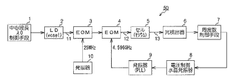
図2は本発明の第1の実施形態に係る原子発振器の構成を示す図である。この原子発振
器50は、波長が異なるコヒーレント光対を2対以上(後述するように3対)の共鳴光を
入射したときの量子干渉効果による光吸収特性を利用して発振周波数を制御する原子発振
器であって、各共鳴光を出射するLD(VCSEL)(コヒーレント光源)2と、LD2
の中心波長を発生する中心波長発生手段1と、二つの異なる基底状態のエネルギー差(Δ
E12)に相当する周波数(9.2GHz)の1/2(4.596GHz)を発振する発
振器9と、約25MHzの周波数を発振する発振器10と、電気信号によりLD2から出
射された共鳴光11に周波数変調を与えるEOM(電気光学変調素子)3、4と、EOM
4により変調された光12の波長により光の吸収量を変化させる、気体状セシウム(アル
カリ金属として)原子を封入したガスセル5と、ガスセル5から透過する光13を検出す
る光検出器(光検出手段)6と、光検出器6の出力に基づきガスセル5のEIT状態を検
出して出力電圧を制御する周波数制御手段7と、を備えて構成されている。尚、発振器1
0の発振周波数は25MHzとしたが、この周波数はセシウム原子の典型的なドップラー
幅(例えば室温で約1GHz)に対して十分小さい値である。この周波数は適宜変更する
ことができる。また、発振器9の出力周波数は、セシウムの場合ΔE12に相当する周波
数が約9.2GHz(4.596GHz×2)であるので、4.596GHzとし、周波
数制御手段7から出力される制御電圧により電圧制御水晶発振器8を制御して得られた周
波数を逓倍して生成される。そして、発振器10の周波数(25MHz)によりEOM3
を変調し、発振器9の周波数(4.596GHz)によりEOM4を変調して、EOM3
とEOM4をLD2の出射側に直列に配置した。尚、EOM3と発振器10の組み合わせ
と、EOM4と発振器9の組み合わせの配列順序を逆にしても構わない。
FIG. 2 is a diagram showing a configuration of the atomic oscillator according to the first embodiment of the present invention. This atomic oscillator 50 is an atomic oscillator that controls the oscillation frequency using light absorption characteristics due to the quantum interference effect when two or more pairs of coherent light beams having different wavelengths (three pairs as will be described later) are incident. An LD (VCSEL) (coherent light source) 2 that emits each resonance light, and LD2
The center wavelength generating means 1 for generating the center wavelength of the two and the energy difference (Δ
E12), an oscillator 9 that oscillates ½ (4.596 GHz) of a frequency (9.2 GHz), an
A gas cell 5 in which gaseous cesium (as an alkali metal) is encapsulated, which changes the amount of light absorption depending on the wavelength of the light 12 modulated by 4, and a photodetector (light detection) that detects light 13 transmitted from the gas cell 5. Means) 6 and frequency control means 7 for detecting the EIT state of the gas cell 5 based on the output of the photodetector 6 and controlling the output voltage.
Although the oscillation frequency of 0 is 25 MHz, this frequency is sufficiently small with respect to a typical Doppler width of cesium atoms (for example, about 1 GHz at room temperature). This frequency can be changed as appropriate. The output frequency of the oscillator 9 is 4.596 GHz because the frequency corresponding to ΔE12 in the case of cesium is about 9.2 GHz (4.596 GHz × 2), and the voltage is controlled by the control voltage output from the frequency control means 7. It is generated by multiplying the frequency obtained by controlling the
EOM4 is modulated by the frequency of the oscillator 9 (4.596 GHz), and EOM3
And EOM4 are arranged in series on the emission side of LD2. Note that the arrangement order of the combination of the
即ち、本実施形態の原子発振器50の構成が従来と異なる点は、LD2から出射された
共鳴光11に対し変調手段としてEOM3を介すことで、波長が異なる2つの共鳴光対を
2対以上(3対)とした点である。従来の原子発振器では、波長の異なる2つの共鳴光対
を1対のみ用意して、同時に照射される2つの共鳴光の周波数差(波長の差)が正確に夫
々の基底準位のエネルギー差ΔE12に一致するように周波数を制御していた。しかし、
原子の運動による共鳴光のドップラー効果の為、ガスセル5内に閉じ込められたセシウム
原子集団の共鳴光波長には分布が生じ、1対の共鳴光では、偶然その波長に対応する共鳴
条件を満たす速度で運動している一部のセシウム原子としか相互作用をおこさないので、
EIT現象を発生する効率が悪かった。そこで本実施形態では、波長の異なる少なくとも
4つ(2つの共鳴光対)の共鳴光をガスセル5に封入された気体状のセシウム原子と相互
作用させるように光変調手段を構成した。これにより、ガスセル5内で単位体積あたりで
EIT現象に寄与するセシウム原子の数を増大させることが可能となり、効率よくEIT
信号を取得することができる。
That is, the configuration of the atomic oscillator 50 of the present embodiment is different from the conventional one in that two or more resonance light pairs having different wavelengths can be obtained by passing the
Due to the Doppler effect of the resonant light due to the movement of atoms, a distribution occurs in the resonant light wavelength of the cesium atom group confined in the gas cell 5, and the speed that satisfies the resonant condition corresponding to that wavelength by chance with a pair of resonant lights. Only interact with some of the cesium atoms moving in
The efficiency of generating the EIT phenomenon was poor. Therefore, in the present embodiment, the light modulation means is configured so that at least four (two resonance light pairs) having different wavelengths interact with gaseous cesium atoms sealed in the gas cell 5. This makes it possible to increase the number of cesium atoms that contribute to the EIT phenomenon per unit volume in the gas cell 5, and to efficiently perform EIT.
A signal can be acquired.
図3(a)及び(b)はガスセルに入射する共鳴光の周波数スペクトラムを示す図であ
る。図4はガスセルに入射した共鳴光と気体状のセシウム原子の移動方向の様子を示す図
である。
次に本実施形態の動作について図3及び図4を参照しながら説明する。LD2の共鳴光
11は中心波長がλ0(中心周波数f0)となるように中心波長制御手段1で制御される
。LD2の共鳴光11に対して、EOM3と4で周波数変調をかけると、ガスセル5には
、図3(a)に示す周波数スペクトラム30〜32を有する共鳴光12が入力される。こ
こで、図3(a)において、A−A´の周波数差は9.2GHzであり、この一対の共鳴
光に対しては、λ0を適当な値に設定することで図4に示す入射光12の方向に対する速
度成分が小さい気体状のセシウム原子15がEIT現象を発生する。また、B−B´の周
波数差も9.2GHzであり、この一対の共鳴光に対しては、図4に示す入射光12と反
対方向の速度成分を持つ気体状のセシウム原子14がEIT現象を発生する。また、図3
(a)において、C−C´の周波数差も9.2GHzであり、この一対の共鳴光に対して
は、図4に示す入射光12と同じ方向の速度成分を持つ気体状のセシウム原子16がEI
T現象を発生する。このように、ガスセル5内の原子は様々な速度分布を持っている。そ
こで上記のようにサイドバンドB、B´、C、C´の成分を与えた共鳴光12をガスセル
5に入射すると、A−A´、B−B´、及びC−C´の周波数差は何れも9.2GHzと
なり、これら3対のレーザー光はいずれも対応する速度成分を持つ気体状のセシウム原子
と相互作用を起こし、その結果EIT現象に寄与するセシウム原子の割合が増大する。こ
れにより、信号対雑音比(S/N比)の大きい所望のEIT信号を得ることができる。
FIGS. 3A and 3B are diagrams showing the frequency spectrum of the resonant light incident on the gas cell. FIG. 4 is a diagram illustrating the state of the resonance light incident on the gas cell and the moving direction of gaseous cesium atoms.
Next, the operation of this embodiment will be described with reference to FIGS. The
In (a), the frequency difference of CC ′ is also 9.2 GHz, and for this pair of resonance lights, gaseous cesium atoms 16 having velocity components in the same direction as the incident light 12 shown in FIG. EI
T phenomenon occurs. Thus, the atoms in the gas cell 5 have various velocity distributions. Therefore, when the
尚、本実施形態ではEOM4の変調周波数を気体状のセシウム原子の周波数差の1/2
(4.596GHz)としたが、周波数差の9.2GHzとしても構わない。そのときの
共鳴光の周波数スペクトラムは図3(b)のようになり、周波数スペクトラム33〜35
が発生するが、例えば、周波数スペクトラム33は使用せずに、周波数スペクトラム34
と35(周波数スペクトラム33と34でも可)を使用する。即ち、A−λ0の周波数差
は9.2GHzであり、この一対の共鳴光に対しては、λ0を適当な値に設定することで
図4に示す入射光12の方向に対する速度成分が小さい気体状のセシウム原子15がEI
T現象を発生する。B−λ1の周波数差も9.2GHzであり、この一対の共鳴光に対し
ては、図4に示す入射光12と反対方向の速度成分を持つ気体状のセシウム原子14がE
IT現象を発生する。また、C−λ2の周波数差も9.2GHzであり、この一対の共鳴
光に対しては、図4に示す入射光12と同じ方向の速度成分を持つ気体状のセシウム原子
16がEIT現象を発生する。このように、ガスセル5内の原子は様々な速度分布を持っ
ている。そこで上記のようにサイドバンドB、λ1、C、λ2の成分を与えた共鳴光12
をガスセル5に入射すると、A−λ0、B−λ1、及びC−λ2の周波数差は何れも9.
2GHzとなり、これら3対のレーザー光はいずれも対応する速度成分を持つ気体状のセ
シウム原子と相互作用を起こし、その結果EIT現象に寄与するセシウム原子の割合が増
大する。これにより、信号対雑音比(S/N比)の大きい所望のEIT信号を得ることが
できる。
In this embodiment, the modulation frequency of EOM4 is set to 1/2 of the frequency difference of gaseous cesium atoms.
(4.596 GHz), but the frequency difference may be 9.2 GHz. The frequency spectrum of the resonant light at that time is as shown in FIG.
For example, the
And 35 (
T phenomenon occurs. The frequency difference of B-λ1 is also 9.2 GHz. For this pair of resonant lights, gaseous cesium atoms 14 having velocity components in the opposite direction to the incident light 12 shown in FIG.
An IT phenomenon occurs. Also, the frequency difference of C-λ2 is 9.2 GHz, and for this pair of resonant lights, gaseous cesium atoms 16 having velocity components in the same direction as the incident light 12 shown in FIG. Occur. Thus, the atoms in the gas cell 5 have various velocity distributions. Therefore, as described above, the
Is incident on the gas cell 5, the frequency differences of A−
All of these three pairs of laser beams interact with gaseous cesium atoms having a corresponding velocity component, and as a result, the proportion of cesium atoms contributing to the EIT phenomenon increases. Thereby, a desired EIT signal having a large signal-to-noise ratio (S / N ratio) can be obtained.
即ち、少なくとも2つの共鳴光対(ここでは3対)の共鳴光を発生させるためには、L
D2から出射される共鳴光にサイドバンドを重畳させて発生させ、その周波数スペクトラ
ムを利用することが考えられる。また、共鳴光を変調する周波数は、二つの異なる基底状
態のエネルギー差(ΔE12)に相当する周波数(9.2GHz)の1/2の4.596
GHzと、セシウム原子の典型的なドップラー幅(例えば室温で約1GHz)に対して十
分小さい値である周波数(ここでは25MHz)によって変調する必要がある。また、光
を変調するためのEOMを利用する。そこで本実施形態では、2種類の周波数を夫々発振
する発振器9、10を用意して、LD2の出射側に直列に配置したEOM3と4、を夫々
の周波数で変調する。これにより、LD2から出射した共鳴光11から、9.2GHzの
周波数差を維持した3対の周波数スペクトラムを有する共鳴光を生成することができる。
また、本実施形態ではEOM3とEOM4を1個ずつ備えたが、EOM4と、少なくと
も2つ以上のEOM3をLD2の出射側に直列に配置するようにしても良い。これにより
、共鳴光対の数を任意に設定し、櫛歯様の周波数間隔で発生させることができる。
That is, in order to generate resonance light of at least two resonance light pairs (here, 3 pairs), L
It can be considered that sidebands are superimposed on the resonance light emitted from D2, and the frequency spectrum is used. The frequency for modulating the resonant light is 4.596 which is 1/2 of the frequency (9.2 GHz) corresponding to the energy difference (ΔE12) between two different ground states.
It is necessary to modulate by GHz and a frequency (here, 25 MHz) that is sufficiently small for a typical Doppler width of cesium atoms (eg, about 1 GHz at room temperature). Also, an EOM for modulating light is used. Therefore, in this embodiment,
In this embodiment, one
図5は原子運動によるエネルギーのドップラー拡がりと本発明の共鳴光との関係を説明
する模式図である。容器に封入された気体状のアルカリ金属原子集団のエネルギー状態図
は、図12に示した一つの原子に対するエネルギー状態図の励起準位をドップラー拡がり
に相当するエネルギー帯で置き換えることで表現できる。図5における20、21、22
の各準位は、図4における、それぞれ16、15、14で示された原子に対応する励起準
位である。これにより、速度分布を持った気体状のアルカリ金属原子集団に対して、複数
の共鳴光の対によりEIT現象に寄与する原子の割合が増大していることがわかる。そこ
で、例えば1対の共鳴光に割り当てられるパワーが従来のパワーにほぼ等しい設定にすれ
ば、吸収の飽和限界が高くなりトータルのパワーが増大するので、高いコントラストのE
IT信号が取得できる。また、トータルの光照射パワーが従来とほぼ等しい場合は、本発
明の1対の共鳴光あたりのパワーは減少するので、EIT信号のパワーブロードニング(
光パワーが強いと、EIT信号の線幅が増大してしまう現象)が抑えられ、従来に比べ、
半値幅が狭い良好なEIT信号が取得できる。従ってこれを発振器に適用した場合、周波
数安定性を従来より向上させることができる。
FIG. 5 is a schematic diagram illustrating the relationship between the Doppler spread of energy due to atomic motion and the resonant light of the present invention. The energy state diagram of the gaseous alkali metal atom group enclosed in the container can be expressed by replacing the excitation level of the energy state diagram for one atom shown in FIG. 12 with an energy band corresponding to the Doppler broadening. 20, 21, 22 in FIG.
4 are excitation levels corresponding to atoms indicated by 16, 15, and 14, respectively, in FIG. Thereby, it can be seen that the ratio of atoms contributing to the EIT phenomenon is increased by a plurality of pairs of resonance light with respect to a gaseous alkali metal atom group having a velocity distribution. Therefore, for example, if the power allocated to a pair of resonant lights is set to be approximately equal to the conventional power, the saturation limit of absorption increases and the total power increases, so that a high contrast E
IT signal can be acquired. In addition, when the total light irradiation power is substantially equal to the conventional one, the power per pair of resonant light of the present invention is reduced, so that the power broadening of the EIT signal (
If the optical power is strong, the phenomenon that the line width of the EIT signal increases) is suppressed.
A good EIT signal with a narrow half-value width can be acquired. Therefore, when this is applied to an oscillator, the frequency stability can be improved as compared with the prior art.
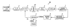
図6は本発明の第2の実施形態に係る原子発振器の構成を示す図である。同じ構成要素
には図2と同じ参照番号を付して説明する。図6が図2と異なる点は、EOM4を削除し
て、発振器10、及び発振器9の出力信号を混合する混合器17を備え、混合器17の出
力信号18によりEOM3を駆動して、EOM3をLD2の出射側に配置する。これによ
り、EOM3から出射される共鳴光12は、図3(a)と同様の周波数スペクトラムを発
生する。
即ち、光を変調するためには、EOMを用いているが、周波数スペクトラムの数を増や
すと、それだけEOMの数を増やさなければならず、コスト的に高くなり、且つ部品点数
が増加するといった問題がある。そこで本実施形態では、EOMを変調する信号を予め混
合器17により混合しておき、その出力信号18により1つのEOM3を変調する。これ
により、EOMの数を最小限にして、部品点数を削減することができる。
FIG. 6 is a diagram showing a configuration of an atomic oscillator according to the second embodiment of the present invention. The same components will be described with the same reference numerals as in FIG. 6 differs from FIG. 2 in that the EOM 4 is deleted and the
That is, EOM is used to modulate light. However, if the number of frequency spectrums is increased, the number of EOMs must be increased accordingly, resulting in an increase in cost and the number of parts. There is. Therefore, in the present embodiment, a signal for modulating the EOM is previously mixed by the
図7は本発明の第3の実施形態に係る原子発振器の構成を示す図である。同じ構成要素
には図6と同じ参照番号を付して説明する。図7が図6と異なる点は、EOM3を削除し
て、混合器17の出力信号19により直接LD2を変調駆動する。これにより、LD2か
ら出射される共鳴光11は、図3(a)と同様の周波数スペクトラムを発生する。
即ち、LD2から出射された共鳴光11は、中心波長がλ0となるように中心波長制御
手段1で制御されている。そして、中心波長を変調するためには、LD2から出射された
共鳴光11をEOMで変調する方法以外に、LD2そのものを変調する方法がある。そこ
で本実施形態では、発振器10、及び発振器9の出力周波数を混合する混合器17により
混合された信号19でLD2そのものを変調駆動する。これにより、EOMを不要とする
ことができる。また、発振器10の出力周波数は、電圧制御水晶発振器8からPLL等を
介して(発振器9の回路の一部を利用することもできる)生成することもできる。その場
合は発振器10も不要となる。
また、図示は省略するが、従来のEIT方式による原子発振器に備えられているLDを
、夫々異なる波長の面発光レーザーをアレイ状に配置した構成としても構わない。
FIG. 7 is a diagram showing a configuration of an atomic oscillator according to the third embodiment of the present invention. The same components will be described with the same reference numerals as in FIG. 7 differs from FIG. 6 in that the
That is, the
Although not shown, the LD provided in the conventional atomic oscillator of the EIT system may have a configuration in which surface emitting lasers having different wavelengths are arranged in an array.
図8は本発明の実施形態に係る磁気センサーの構成を示す図である。同じ構成要素には
図7と同じ参照番号を付して説明する。図8が図7と異なる点は、ガスセル5の近傍に、
被測定磁気発生源37を配し、周波数制御手段7の出力信号の変動を測定する磁気測定器
36と、を備えた点である。原子発振器の発振周波数は、原子の2つの基底準位間のエネ
ルギー差(ΔE12)を基準としている。ΔE12の値は、外部磁気の強さやゆらぎで変
化するため、原子発振器のセルには、外部磁気の影響を受けないように、磁気シールドが
施されている。そこで磁気シールドを外し、ΔE12の変化を発振周波数変化から読取る
ことにより、外部磁気の強さや変動を測定する磁気センサーをつくることができる。本発
明の構成とすることにより、S/N比の高い状態でEIT現象を発現させることができる
ため、磁気センサーの小型化が可能となる。
FIG. 8 is a diagram showing the configuration of the magnetic sensor according to the embodiment of the present invention. The same components will be described with the same reference numerals as in FIG. 8 differs from FIG. 7 in the vicinity of the gas cell 5,
And a magnetic measuring device 36 for measuring the fluctuation of the output signal of the frequency control means 7 by providing a measured
図9(a)は、波長の異なる2つの共鳴光対によるEIT現象に係る光透過強度の図で
あり、図9(b)は波長の異なる2つの共鳴光対を変調したときのEIT現象に係る光透
過強度の図である。図9(a)から、波形41はVCSELからの直線偏光された光透過
強度の波形であり、その共鳴光対を更に波長板を通過させて円偏光としたときの光透過強
度が波形42である。波形42は波形41に対して約20%レベルが増加しているのが分
かる。また、図9(b)のように共鳴光対を変調すると、複数の共鳴光対はいずれも対応
する速度分布を持つ気体状のセシウム原子と相互作用を起こし、複数のピークを持った波
形43が発現する。本実施形態では、例えば、図10のようにLD2とガスセル5の間に
波長板40を光路と直交するように配置して、波長板面を徐々に回転すると共鳴光対11
が円偏光となったときに、波長λ0で光透過強度が最大の波形45となることが確認され
た。従って、共鳴光対を直線偏光から円偏光に変化する過程で光透過強度が波形43(直
線偏光)、波形44(楕円偏光)、波形45(円偏光)となることが確認された。
即ち、LD2から出射される共鳴光対11は光の伝播方向に垂直な面内で、電気ベクト
ルの先端が円を描く場合、その光は円偏光と呼ばれる。共鳴光対を円偏光に変換すると、
波長λ0の光透過強度が通常の約6倍に増大することが実験的に確認されている。これに
より、EIT現象による光出力信号のSN比を向上させることができる。
また、LD2から出射される共鳴光対11は光の伝播方向に垂直な面内で、電気ベクト
ルの先端が楕円を描く場合、その光は楕円偏光と呼ばれる。共鳴光対の光路上に光路と直
交するように波長板を置いてその面を回転させると、偏光状態が変化して直交偏光と円偏
光の間に連続的に変化する楕円偏光が存在することが分かる。従って、楕円偏光であって
もEIT現象による光出力信号のSN比を向上させることができる。
FIG. 9A is a diagram of the light transmission intensity related to the EIT phenomenon by two resonant light pairs having different wavelengths, and FIG. 9B shows the EIT phenomenon when the two resonant light pairs having different wavelengths are modulated. It is a figure of the light transmission intensity which concerns. From FIG. 9A, the waveform 41 is a linearly polarized light transmission intensity waveform from the VCSEL, and the light transmission intensity when the resonant light pair is further passed through the wave plate to be circularly polarized is the waveform 42. is there. It can be seen that the waveform 42 is about 20% higher than the waveform 41. When the resonant light pair is modulated as shown in FIG. 9B, each of the plurality of resonant light pairs interacts with gaseous cesium atoms having a corresponding velocity distribution, and has a
It was confirmed that when the light becomes circularly polarized light, the
That is, the resonant
It has been experimentally confirmed that the light transmission intensity at the wavelength λ0 is increased to about 6 times the usual. Thereby, the S / N ratio of the optical output signal due to the EIT phenomenon can be improved.
Further, when the
図10は、本発明の第4の実施形態に係る原子発振器の構成を示す図である。第4の実
施形態は、図7の構成に波長板40を追加した構成である。即ち、LD2とセル5の間に
波長板40を光路と直交するように配置したものである。LD2から出射した直線偏光の
共鳴光対11は波長板40に入射して、90度位相が偏光されて円偏光11aとなる。尚
、波長板40はLD2とセル5の間であれば何処でも良く、LD2の出射面の近傍や、セ
ル5の入射口の近傍でも構わない。
FIG. 10 is a diagram illustrating a configuration of an atomic oscillator according to the fourth embodiment of the present invention. In the fourth embodiment, a
図11は、本発明の第5の実施形態に係る原子発振器の構成を示す図である。第5の実
施形態は、図6の構成に波長板40を追加した構成である。即ち、EOM3とセル5の間
に波長板40を光路と直交するように配置したものである。LD2から出射した直線偏光
の共鳴光対11はEOM3により変調されて共鳴光12となり、波長板40に入射して、
90度位相が偏光されて円偏光12aとなる。尚、波長板40はEOM3とセル5の間で
あれば何処でも良く、EOM3の出射面の近傍や、セル5の入射口の近傍でも構わない。
即ち、波長板とは、直交する偏光成分の間に位相差を生じさせる複屈折素子のことであ
る。位相差π(180°)を生じるものをλ/2板または半波長板と呼び、直線偏光の偏
光方向を変えるために用いる。位相差π/2(90°)を生じるものをλ/4板または四
分の一波長板と呼び、直線偏光を円偏光(楕円偏光)に変換、また逆に円偏光(楕円偏光
)を直線偏光に変換するために用いる。本実施形態では、直線偏光を円偏光又は楕円偏光
に変える必要があるため、λ/4板が使用され、LD2から出射した直線偏光の共鳴光対
11を波長板40により円偏光又は楕円偏光に変えて、ガスセル5に入射させる必要があ
る。これにより、簡単な構成でEIT現象による光出力信号のSN比を向上させることが
できる。
FIG. 11 is a diagram showing a configuration of an atomic oscillator according to the fifth embodiment of the invention. In the fifth embodiment, a
The 90-degree phase is polarized to become circularly polarized light 12a. The
That is, the wave plate is a birefringent element that generates a phase difference between orthogonal polarization components. A plate that generates a phase difference π (180 °) is called a λ / 2 plate or a half-wave plate, and is used to change the polarization direction of linearly polarized light. Those that produce a phase difference of π / 2 (90 °) are called λ / 4 plates or quarter-wave plates, and convert linearly polarized light into circularly polarized light (elliptically polarized light). Used to convert to polarized light. In this embodiment, since it is necessary to change linearly polarized light into circularly polarized light or elliptically polarized light, a λ / 4 plate is used, and the linearly polarized resonant
1 中心波長制御手段、2 LD、3 EOM、4 EOM、5 ガスセル、6 光検
出器、7 周波数制御手段、8 電圧制御水晶発振器、9 発振器、10 発振器、11
、12、13 共鳴光、14、15、16 気体状のセシウム原子、17 混合器18、
19 変調信号、40 波長板、41 変調をかけないときの直線偏光された波形、42
変調をかけないときの円偏光された波形、43 変調をかけたときの直線偏光された波
形、44 変調をかけたときの楕円偏光された波形、45 変調をかけたときの円偏光さ
れた波形、50、51、52、53、54 原子発振器
1 center wavelength control means, 2 LD, 3 EOM, 4 EOM, 5 gas cell, 6 photodetector, 7 frequency control means, 8 voltage control crystal oscillator, 9 oscillator, 10 oscillator, 11
, 12, 13 Resonant light, 14, 15, 16 Gaseous cesium atoms, 17
19 modulation signal, 40 wave plate, 41 linearly polarized waveform without modulation, 42
Circularly polarized waveform without modulation, 43 Linearly polarized waveform with modulation, 44 Elliptically polarized waveform with modulation, 45 Circularly polarized waveform with modulation , 50, 51, 52, 53, 54 Atomic oscillator
Claims (12)
前記光源から入射された光を第1の発振信号及び第2の発振信号に基づき変調し、前記複数の共鳴光対を含む光を出射する変調手段と、を備えることを特徴とする請求項1乃至3のいずれか一項に記載の量子干渉装置。 A light source;
2. A modulation unit that modulates light incident from the light source based on a first oscillation signal and a second oscillation signal and emits light including the plurality of resonance light pairs. The quantum interference device according to any one of claims 1 to 3 .
前記第1の発振信号に基づき入射された光を変調して出射する第1の電気光学変調素子、及び前記第2の発振信号に基づき入射された光を変調して出射する第2の電気光学変調素子を有し、前記第1の電気光学変調素子と前記第2の電気光学変調素子が直列に接続されている構成を備えることを特徴とする請求項4に記載の量子干渉装置。 The modulating means includes
A first electro-optic modulation element that modulates and emits incident light based on the first oscillation signal, and a second electro-optic that modulates and emits incident light based on the second oscillation signal The quantum interference device according to claim 4 , further comprising: a modulation element, wherein the first electro-optic modulation element and the second electro-optic modulation element are connected in series.
前記第1の発振信号及び前記第2の発振信号を混合する混合手段と、
前記混合手段の出力信号に基づき前記光源から入射された前記光を変調して出射する電気光学変調素子と、を備えることを特徴とする請求項4に記載の量子干渉装置。 The modulating means includes
Mixing means for mixing the first oscillation signal and the second oscillation signal;
The quantum interference device according to claim 4 , further comprising: an electro-optic modulation element that modulates and emits the light incident from the light source based on an output signal of the mixing unit.
前記光源から出射された前記光が前記複数の共鳴光対を含む光であることを特徴とする請求項1乃至3のいずれか一項に記載の量子干渉装置。 A light source that emits light modulated based on a signal obtained by mixing the first oscillation signal and the second oscillation signal;
Quantum interference device according to any one of claims 1 to 3, wherein the light emitted from the light source is a light including a plurality of resonant light pair.
前記複数の共鳴光対を含む光は、
周波数がf0− f2− f1の第1の共鳴光、周波数がf0− f2の第2の共鳴光、周波数がf0− f2+f1の第3の共鳴光、周波数がf0− f1の第4の共鳴光、周波数がf0の第5の共鳴光、周波数がf0+f1の第6の共鳴光、周波数がf0+f2− f1の第7の共鳴光、周波数がf0+f2の第8の共鳴光、及び周波数がf0+f2+f1の第9の共鳴光を含む光であることを特徴とする請求項4乃至7のいずれか一項に記載の量子干渉装置。 When the frequency of the first oscillation signal is f1, the frequency of the second oscillation signal is f2, and the frequency or center frequency of light emitted from the light source is f0,
The light including the plurality of resonance light pairs is
A first resonant light having a frequency of f0-f2-f1, a second resonant light having a frequency of f0-f2, a third resonant light having a frequency of f0-f2 + f1, a fourth resonant light having a frequency of f0-f1, A fifth resonant light having a frequency of f0, a sixth resonant light having a frequency of f0 + f1, a seventh resonant light having a frequency of f0 + f2-f1, an eighth resonant light having a frequency of f0 + f2, and a ninth resonant light having a frequency of f0 + f2 + f1 The quantum interference device according to claim 4 , wherein the quantum interference device is light including resonance light.
Priority Applications (9)
| Application Number | Priority Date | Filing Date | Title |
|---|---|---|---|
| JP2009153402A JP5381400B2 (en) | 2009-02-06 | 2009-06-29 | Quantum interferometers, atomic oscillators, and magnetic sensors |
| US12/699,350 US8237514B2 (en) | 2009-02-06 | 2010-02-03 | Quantum interference device, atomic oscillator, and magnetic sensor |
| CN201210403436.6A CN102882521B (en) | 2009-02-06 | 2010-02-05 | Quantum interference device, atomic oscillator and magnetic sensor |
| CN201210454371.8A CN102931987B (en) | 2009-02-06 | 2010-02-05 | Quantum interference device, atomic oscillator and magnetic sensor |
| CN201210405065.5A CN102882522B (en) | 2009-02-06 | 2010-02-05 | Quantum interference device, atomic oscillator and magnetic sensor |
| CN201010113602XA CN101800545B (en) | 2009-02-06 | 2010-02-05 | Quantum interference device, atomic oscillator, and magnetic sensor |
| US13/419,789 US8643441B2 (en) | 2009-02-06 | 2012-03-14 | Quantum interference device, atomic oscillator, and magnetic sensor |
| US13/541,147 US20120267509A1 (en) | 2009-02-06 | 2012-07-03 | Quantum interference device, atomic oscillator, and magnetic sensor |
| US14/588,624 US9507179B2 (en) | 2009-02-06 | 2015-01-02 | Quantum interference device, atomic oscillator, and magnetic sensor |
Applications Claiming Priority (3)
| Application Number | Priority Date | Filing Date | Title |
|---|---|---|---|
| JP2009025652 | 2009-02-06 | ||
| JP2009025652 | 2009-02-06 | ||
| JP2009153402A JP5381400B2 (en) | 2009-02-06 | 2009-06-29 | Quantum interferometers, atomic oscillators, and magnetic sensors |
Related Child Applications (1)
| Application Number | Title | Priority Date | Filing Date |
|---|---|---|---|
| JP2013161510A Division JP5720740B2 (en) | 2009-02-06 | 2013-08-02 | Quantum interferometers, atomic oscillators, and magnetic sensors |
Publications (3)
| Publication Number | Publication Date |
|---|---|
| JP2010206767A JP2010206767A (en) | 2010-09-16 |
| JP2010206767A5 JP2010206767A5 (en) | 2012-07-26 |
| JP5381400B2 true JP5381400B2 (en) | 2014-01-08 |
Family
ID=42967314
Family Applications (4)
| Application Number | Title | Priority Date | Filing Date |
|---|---|---|---|
| JP2009153402A Active JP5381400B2 (en) | 2009-02-06 | 2009-06-29 | Quantum interferometers, atomic oscillators, and magnetic sensors |
| JP2009201329A Active JP5540607B2 (en) | 2009-02-06 | 2009-09-01 | Quantum interference device, atomic oscillator, magnetic sensor, and quantum interference sensor |
| JP2013161510A Active JP5720740B2 (en) | 2009-02-06 | 2013-08-02 | Quantum interferometers, atomic oscillators, and magnetic sensors |
| JP2015063768A Active JP5954457B2 (en) | 2009-02-06 | 2015-03-26 | Quantum interference device |
Family Applications After (3)
| Application Number | Title | Priority Date | Filing Date |
|---|---|---|---|
| JP2009201329A Active JP5540607B2 (en) | 2009-02-06 | 2009-09-01 | Quantum interference device, atomic oscillator, magnetic sensor, and quantum interference sensor |
| JP2013161510A Active JP5720740B2 (en) | 2009-02-06 | 2013-08-02 | Quantum interferometers, atomic oscillators, and magnetic sensors |
| JP2015063768A Active JP5954457B2 (en) | 2009-02-06 | 2015-03-26 | Quantum interference device |
Country Status (2)
| Country | Link |
|---|---|
| JP (4) | JP5381400B2 (en) |
| CN (3) | CN102882522B (en) |
Families Citing this family (22)
| Publication number | Priority date | Publication date | Assignee | Title |
|---|---|---|---|---|
| JP2001028345A (en) * | 1999-07-15 | 2001-01-30 | Sony Corp | Manufacture of semiconductor device |
| US8237514B2 (en) | 2009-02-06 | 2012-08-07 | Seiko Epson Corporation | Quantum interference device, atomic oscillator, and magnetic sensor |
| JP5381400B2 (en) * | 2009-02-06 | 2014-01-08 | セイコーエプソン株式会社 | Quantum interferometers, atomic oscillators, and magnetic sensors |
| JP5880807B2 (en) * | 2011-03-09 | 2016-03-09 | セイコーエプソン株式会社 | Coherent light source |
| JP5818000B2 (en) * | 2011-12-09 | 2015-11-18 | セイコーエプソン株式会社 | Atomic oscillator, control method of atomic oscillator, and quantum interference device |
| EP2639277A1 (en) | 2012-03-13 | 2013-09-18 | Nitto Denko Corporation | Heat-resistant pressure-sensitive adhesive tape for production of semiconductor device and method for producing semiconductor device using the tape |
| JP6069886B2 (en) * | 2012-05-16 | 2017-02-01 | セイコーエプソン株式会社 | Quantum interference device, atomic oscillator, electronic device, and quantum interference method |
| JP6136110B2 (en) * | 2012-05-16 | 2017-05-31 | セイコーエプソン株式会社 | Quantum interference device, atomic oscillator and electronic equipment |
| JP2014022667A (en) * | 2012-07-20 | 2014-02-03 | Ricoh Co Ltd | Vertical cavity surface emitting laser element, and atomic oscillator |
| JP6124536B2 (en) * | 2012-08-30 | 2017-05-10 | 株式会社リコー | Atomic oscillator and CPT resonance excitation method |
| JP6094750B2 (en) * | 2013-03-29 | 2017-03-15 | セイコーエプソン株式会社 | Quantum interference device, atomic oscillator, magnetic sensor, and method of manufacturing quantum interference device |
| JP6142989B2 (en) * | 2013-03-29 | 2017-06-07 | セイコーエプソン株式会社 | Quantum interference device, atomic oscillator, magnetic sensor, and method of manufacturing quantum interference device |
| JP2015089055A (en) * | 2013-11-01 | 2015-05-07 | セイコーエプソン株式会社 | Optical module and atomic oscillator |
| US9726494B2 (en) | 2014-05-15 | 2017-08-08 | Northrop Grumman Systems Corporation | Atomic sensor system |
| JP6529230B2 (en) * | 2014-08-28 | 2019-06-12 | ニッカ電測株式会社 | Metal detection device |
| CN105515580B (en) | 2014-10-14 | 2020-07-14 | 精工爱普生株式会社 | Quantum interference device, atomic oscillator, electronic apparatus, and moving object |
| JP6544132B2 (en) | 2015-08-17 | 2019-07-17 | セイコーエプソン株式会社 | Quantum interference device, atomic oscillator, and electronic device |
| JP6753232B2 (en) * | 2016-09-07 | 2020-09-09 | セイコーエプソン株式会社 | Atomic oscillators, electronics and mobiles |
| CN110265854B (en) * | 2019-06-18 | 2020-07-10 | 中国人民解放军国防科技大学 | Light guide self-adaptive narrow-spectrum microwave generation method based on high-energy pulse cluster laser |
| CN110908130A (en) * | 2019-10-31 | 2020-03-24 | 同济大学 | Method for realizing full-light, broadband and low-noise polarization revolving door |
| JP7443862B2 (en) | 2020-03-23 | 2024-03-06 | セイコーエプソン株式会社 | Resonance generation method and atomic oscillator |
| CN112083358B (en) * | 2020-08-28 | 2023-03-14 | 之江实验室 | Laser frequency stabilization system for SERF ultrahigh sensitive magnetic field measuring device |
Family Cites Families (22)
| Publication number | Priority date | Publication date | Assignee | Title |
|---|---|---|---|---|
| JP2567897B2 (en) * | 1988-02-16 | 1996-12-25 | 富士通株式会社 | Semiconductor laser device |
| JP3172776B2 (en) * | 1992-05-19 | 2001-06-04 | アンリツ株式会社 | Atomic oscillator |
| JPH08335876A (en) * | 1995-06-09 | 1996-12-17 | Fujitsu Ltd | Rubidium atomic oscillator |
| BR9916506A (en) * | 1998-12-24 | 2001-09-11 | Reckitt Benckiser Uk Ltd | Method and apparatus for dispensing a volatile composition |
| US6320472B1 (en) * | 1999-01-26 | 2001-11-20 | Kernco, Inc. | Atomic frequency standard |
| US6201821B1 (en) * | 2000-06-05 | 2001-03-13 | Agilent Technologies, Inc. | Coherent population trapping-based frequency standard having a reduced magnitude of total a.c. stark shift |
| US6359916B1 (en) * | 2000-06-05 | 2002-03-19 | Agilent Technologies, Inc. | Coherent population trapping-based frequency standard and method for generating a frequency standard incorporating a quantum absorber that generates the CPT state with high frequency |
| DE60329666D1 (en) * | 2002-04-09 | 2009-11-26 | California Inst Of Techn | ATOM WATCH BASED ON AN OPTOELECTRONIC OSCILLATOR |
| JP3755001B2 (en) * | 2002-08-30 | 2006-03-15 | 独立行政法人情報通信研究機構 | Atomic oscillation acquisition device and atomic clock |
| US6710663B1 (en) * | 2002-10-25 | 2004-03-23 | Rockwell Collins | Temperature compensation of a rubidium frequency standard |
| US6927636B2 (en) * | 2003-09-03 | 2005-08-09 | Symmetricom, Inc. | Light stabilization for an optically excitable atomic medium |
| JP2005109619A (en) * | 2003-09-29 | 2005-04-21 | Fujitsu Ltd | Atomic oscillator |
| US7378913B2 (en) * | 2003-11-26 | 2008-05-27 | Kernco, Inc. | Optically excited atomic frequency standard |
| US7323941B1 (en) * | 2004-02-18 | 2008-01-29 | Princeton University | Method and system for operating a laser self-modulated at alkali-metal atom hyperfine frequency |
| US7102451B2 (en) * | 2004-02-18 | 2006-09-05 | Princeton University, Office Of Technology, Licensing & Intellectual Property | Method and system for operating an atomic clock with alternating-polarization light |
| US7345553B2 (en) * | 2004-03-18 | 2008-03-18 | Agilent Technologies, Inc. | Method and apparatus for reducing errors due to line asymmetry in devices utilizing coherent population trapping |
| FR2868558B1 (en) * | 2004-03-30 | 2006-06-30 | Centre Nat Rech Scient Cnrse | METHOD FOR GENERATING AN ATOMIC CLOCK SIGNAL WITH COHERENT POPULATION TRAPPING AND CORRESPONDING ATOMIC CLOCK |
| US7202751B2 (en) * | 2004-10-18 | 2007-04-10 | Agilent Inc. | Optically pumped frequency standard with reduces AC stark shift |
| JP2008522411A (en) * | 2004-11-22 | 2008-06-26 | プリンストン ユニバーシティ | Method and system for operating a self-modulated laser with hyperfine vibrations of alkali metal atoms |
| JP2006351086A (en) * | 2005-06-14 | 2006-12-28 | Epson Toyocom Corp | Optical path compensation apparatus and optical pickup using the same |
| JP5132951B2 (en) * | 2007-02-28 | 2013-01-30 | アンリツ株式会社 | Gas cell type atomic oscillator |
| JP5381400B2 (en) * | 2009-02-06 | 2014-01-08 | セイコーエプソン株式会社 | Quantum interferometers, atomic oscillators, and magnetic sensors |
-
2009
- 2009-06-29 JP JP2009153402A patent/JP5381400B2/en active Active
- 2009-09-01 JP JP2009201329A patent/JP5540607B2/en active Active
-
2010
- 2010-02-05 CN CN201210405065.5A patent/CN102882522B/en active Active
- 2010-02-05 CN CN201210454371.8A patent/CN102931987B/en active Active
- 2010-02-05 CN CN201210403436.6A patent/CN102882521B/en active Active
-
2013
- 2013-08-02 JP JP2013161510A patent/JP5720740B2/en active Active
-
2015
- 2015-03-26 JP JP2015063768A patent/JP5954457B2/en active Active
Also Published As
| Publication number | Publication date |
|---|---|
| JP5540607B2 (en) | 2014-07-02 |
| JP2015167355A (en) | 2015-09-24 |
| CN102931987A (en) | 2013-02-13 |
| CN102882521A (en) | 2013-01-16 |
| CN102931987B (en) | 2015-10-14 |
| JP5954457B2 (en) | 2016-07-20 |
| CN102882521B (en) | 2015-09-09 |
| CN102882522B (en) | 2015-08-05 |
| JP5720740B2 (en) | 2015-05-20 |
| JP2014017824A (en) | 2014-01-30 |
| CN102882522A (en) | 2013-01-16 |
| JP2010206767A (en) | 2010-09-16 |
| JP2010206160A (en) | 2010-09-16 |
Similar Documents
| Publication | Publication Date | Title |
|---|---|---|
| JP5381400B2 (en) | Quantum interferometers, atomic oscillators, and magnetic sensors | |
| US8237514B2 (en) | Quantum interference device, atomic oscillator, and magnetic sensor | |
| CN102013891B (en) | Quantum interference device, atomic oscillator and magnetic sensor | |
| US10162021B2 (en) | Magnetic field measurement device | |
| JP5910807B2 (en) | Optical module and atomic oscillator for an atomic oscillator | |
| CN109839606B (en) | Novel atomic magnetometer device and detection method | |
| US20150116046A1 (en) | Optical module and atomic oscillator | |
| JP5045478B2 (en) | Atomic oscillator | |
| JP6142989B2 (en) | Quantum interference device, atomic oscillator, magnetic sensor, and method of manufacturing quantum interference device | |
| US9200964B2 (en) | Optical module and atomic oscillator | |
| JP2005217442A (en) | Wavelength-variable laser device | |
| JP2012049230A (en) | Quantum interference device and method of quantum interference | |
| JP2015082763A (en) | Optical module and atomic oscillator |
Legal Events
| Date | Code | Title | Description |
|---|---|---|---|
| A711 | Notification of change in applicant |
Free format text: JAPANESE INTERMEDIATE CODE: A711 Effective date: 20100705 |
|
| A521 | Written amendment |
Free format text: JAPANESE INTERMEDIATE CODE: A523 Effective date: 20120608 |
|
| A621 | Written request for application examination |
Free format text: JAPANESE INTERMEDIATE CODE: A621 Effective date: 20120608 |
|
| A131 | Notification of reasons for refusal |
Free format text: JAPANESE INTERMEDIATE CODE: A131 Effective date: 20130604 |
|
| A521 | Written amendment |
Free format text: JAPANESE INTERMEDIATE CODE: A523 Effective date: 20130802 |
|
| RD03 | Notification of appointment of power of attorney |
Free format text: JAPANESE INTERMEDIATE CODE: A7423 Effective date: 20130802 |
|
| TRDD | Decision of grant or rejection written | ||
| A01 | Written decision to grant a patent or to grant a registration (utility model) |
Free format text: JAPANESE INTERMEDIATE CODE: A01 Effective date: 20130903 |
|
| A61 | First payment of annual fees (during grant procedure) |
Free format text: JAPANESE INTERMEDIATE CODE: A61 Effective date: 20130916 |
|
| R150 | Certificate of patent or registration of utility model |
Ref document number: 5381400 Country of ref document: JP Free format text: JAPANESE INTERMEDIATE CODE: R150 Free format text: JAPANESE INTERMEDIATE CODE: R150 |
|
| S531 | Written request for registration of change of domicile |
Free format text: JAPANESE INTERMEDIATE CODE: R313531 |
|
| R350 | Written notification of registration of transfer |
Free format text: JAPANESE INTERMEDIATE CODE: R350 |