JP5799740B2 - Recycled wafer reclaim processing method - Google Patents
Recycled wafer reclaim processing method Download PDFInfo
- Publication number
- JP5799740B2 JP5799740B2 JP2011227893A JP2011227893A JP5799740B2 JP 5799740 B2 JP5799740 B2 JP 5799740B2 JP 2011227893 A JP2011227893 A JP 2011227893A JP 2011227893 A JP2011227893 A JP 2011227893A JP 5799740 B2 JP5799740 B2 JP 5799740B2
- Authority
- JP
- Japan
- Prior art keywords
- wafer
- polishing
- oxide film
- peeled
- bond
- Prior art date
- Legal status (The legal status is an assumption and is not a legal conclusion. Google has not performed a legal analysis and makes no representation as to the accuracy of the status listed.)
- Active
Links
Images

Classifications
-
- H—ELECTRICITY
- H01—ELECTRIC ELEMENTS
- H01L—SEMICONDUCTOR DEVICES NOT COVERED BY CLASS H10
- H01L21/00—Processes or apparatus adapted for the manufacture or treatment of semiconductor or solid state devices or of parts thereof
- H01L21/02—Manufacture or treatment of semiconductor devices or of parts thereof
- H01L21/02002—Preparing wafers
- H01L21/02005—Preparing bulk and homogeneous wafers
- H01L21/02032—Preparing bulk and homogeneous wafers by reclaiming or re-processing
-
- H—ELECTRICITY
- H01—ELECTRIC ELEMENTS
- H01L—SEMICONDUCTOR DEVICES NOT COVERED BY CLASS H10
- H01L21/00—Processes or apparatus adapted for the manufacture or treatment of semiconductor or solid state devices or of parts thereof
- H01L21/02—Manufacture or treatment of semiconductor devices or of parts thereof
- H01L21/02041—Cleaning
- H01L21/02082—Cleaning product to be cleaned
- H01L21/02087—Cleaning of wafer edges
-
- H—ELECTRICITY
- H01—ELECTRIC ELEMENTS
- H01L—SEMICONDUCTOR DEVICES NOT COVERED BY CLASS H10
- H01L21/00—Processes or apparatus adapted for the manufacture or treatment of semiconductor or solid state devices or of parts thereof
- H01L21/70—Manufacture or treatment of devices consisting of a plurality of solid state components formed in or on a common substrate or of parts thereof; Manufacture of integrated circuit devices or of parts thereof
- H01L21/71—Manufacture of specific parts of devices defined in group H01L21/70
- H01L21/76—Making of isolation regions between components
- H01L21/762—Dielectric regions, e.g. EPIC dielectric isolation, LOCOS; Trench refilling techniques, SOI technology, use of channel stoppers
- H01L21/7624—Dielectric regions, e.g. EPIC dielectric isolation, LOCOS; Trench refilling techniques, SOI technology, use of channel stoppers using semiconductor on insulator [SOI] technology
- H01L21/76251—Dielectric regions, e.g. EPIC dielectric isolation, LOCOS; Trench refilling techniques, SOI technology, use of channel stoppers using semiconductor on insulator [SOI] technology using bonding techniques
- H01L21/76254—Dielectric regions, e.g. EPIC dielectric isolation, LOCOS; Trench refilling techniques, SOI technology, use of channel stoppers using semiconductor on insulator [SOI] technology using bonding techniques with separation/delamination along an ion implanted layer, e.g. Smart-cut, Unibond
Description
本発明は、イオン注入剥離法を用いた貼り合わせウェーハの製造において、水素イオン等を注入したボンドウェーハをベースウェーハと貼り合わせた後に剥離して貼り合わせウェーハを製造した際に副生される剥離ウェーハの再生加工方法に関する。 In the production of a bonded wafer using an ion implantation delamination method, the present invention provides a delamination produced as a by-product when a bonded wafer is produced by exfoliating after bonding a bond wafer implanted with hydrogen ions or the like to a base wafer. The present invention relates to a wafer processing method.
SOIウェーハの製造方法、特に先端集積回路の高性能化を可能とする薄膜SOIウェーハの製造方法として、イオン注入したウェーハを貼り合わせ後に剥離してSOIウェーハを製造する方法(イオン注入剥離法:スマートカット法(登録商標)とも呼ばれる技術)が注目されている。 A method for manufacturing an SOI wafer, particularly a method for manufacturing a thin-film SOI wafer capable of improving the performance of advanced integrated circuits, is a method of manufacturing an SOI wafer by peeling an ion-implanted wafer after bonding (ion implantation separation method: smart). A technique called a cutting method (registered trademark) is attracting attention.
このイオン注入剥離法は、二枚のシリコンウェーハの内、少なくとも一方に酸化膜を形成すると共に、一方のシリコンウェーハ(ボンドウェーハ)の上面から水素イオンまたは希ガスイオン等のガスイオンを注入し、該ウェーハ内部にイオン注入層(微小気泡層又は封入層とも呼ぶ)を形成する。その後、イオンを注入した方の面を、酸化膜を介して他方のシリコンウェーハ(ベースウェーハ)と密着させ、その後熱処理(剥離熱処理)を加えて微小気泡層を劈開面として一方のウェーハ(ボンドウェーハ)を薄膜状に剥離する。さらに、熱処理(結合熱処理)を加えて強固に結合してSOIウェーハを製造する技術である(特許文献1参照)。この段階では、劈開面(剥離面)がSOI層の表面となっており、SOI膜厚が薄くてかつ均一性も高いSOIウェーハが比較的容易に得られている。 In this ion implantation separation method, an oxide film is formed on at least one of two silicon wafers, and gas ions such as hydrogen ions or rare gas ions are implanted from the upper surface of one silicon wafer (bond wafer), An ion implantation layer (also referred to as a microbubble layer or an encapsulation layer) is formed inside the wafer. After that, the surface into which the ions are implanted is brought into close contact with the other silicon wafer (base wafer) through an oxide film, and then a heat treatment (peeling heat treatment) is applied to form a microbubble layer as a cleaved surface on one wafer (bond wafer). ) In a thin film. Furthermore, it is a technique for manufacturing an SOI wafer by applying heat treatment (bond heat treatment) and bonding firmly (see Patent Document 1). At this stage, the cleaved surface (peeling surface) is the surface of the SOI layer, and an SOI wafer having a thin SOI film thickness and high uniformity can be obtained relatively easily.
また、このイオン注入剥離法では、剥離後のボンドウェーハ(剥離ウェーハ)に対して、再度、研磨やエッチングなどの表面処理を含む再生加工(リフレッシュ加工)を施すことにより、未結合部に生じる段差や、剥離後の面粗さ、注入残存層の影響を、減少もしくは除去し、ウェーハを繰り返し使用することができる。この再生処理の方法に関しては、例えば、特許文献2のように、面取り加工と研磨を組み合わせ、面取り部に存在するイオン注入残存層の影響を取り除いて、研磨する方法が提案されている。 Further, in this ion implantation separation method, a step generated in the unbonded portion is obtained by subjecting the bond wafer (peeled wafer) after separation to reprocessing (refresh processing) including surface treatment such as polishing and etching again. In addition, the influence of the surface roughness after peeling and the implantation remaining layer can be reduced or eliminated, and the wafer can be used repeatedly. With regard to this regeneration processing method, for example, as disclosed in Patent Document 2, a method of polishing by combining chamfering and polishing to remove the influence of an ion implantation residual layer existing in a chamfered portion has been proposed.
また、特許文献3には、剥離ウェーハに対し、両面研磨により約10μm(基板の各面で5μmずつ)の取代で再生研磨を行うことが記載されている。 Further, Patent Document 3 describes that reclaimed polishing is performed on a peeled wafer by double-side polishing with a machining allowance of about 10 μm (5 μm on each side of the substrate).
ボンドウェーハの再生加工においては、加工取代を大きくすると、加工後の表面は、未結合部に生じる段差、剥離による面粗さ、注入残存層の影響等が減少するために、表面欠陥等の品質を高めることができる。
しかしながら、加工取代が大きいと、加工によるウェーハ厚さの減少量が大きくなり、元のウェーハ厚さ(基準厚さ)から乖離する。例えば、ウェーハハンドリング中のたわみ量などの制限により、加工可能な厚さに下限値が設けられている場合に、剥離ウェーハの厚さが当該下限値に近い値であるときには、再生加工ができないことになる。更には、再生加工を繰り返し行うことによって、ウェーハ厚さの減少も進むため、再生加工の繰り返し回数に制限が生じる。この観点から考えると再生加工の取代は少ない方が望ましい。両者のトレードオフの関係より、品質的要求を満たす最小の加工取代を選択し、ウェーハ厚さ変化量を抑制することが理想的となる。
In bond wafer reclamation processing, if the machining allowance is increased, the surface after processing is reduced in steps such as the level difference in the unbonded part, surface roughness due to peeling, and the influence of the residual implantation layer. Can be increased.
However, if the machining allowance is large, the amount of reduction in wafer thickness due to machining increases and deviates from the original wafer thickness (reference thickness). For example, if a lower limit is set for the workable thickness due to limitations such as the amount of deflection during wafer handling, remanufacturing cannot be performed when the thickness of the peeled wafer is close to the lower limit. become. Furthermore, since repetitive processing is repeatedly performed, the wafer thickness is also reduced, so that the number of repetitive processing is limited. From this point of view, it is desirable that the allowance for reclaim processing is small. It is ideal to select the minimum machining allowance that satisfies the quality requirements from the trade-off relationship between the two and to suppress the wafer thickness variation.
ウェーハ加工のための研磨の種類には、大きく分けて、片面研磨と両面研磨がある。両面研磨では、両面研磨機を用いて、上下の研磨クロスでウェーハを挟み込み、均一な荷重をかけて研磨するので、エッジロールオフ量(ウェーハ最外周部のダレの大きさ)などのウェーハのフラットネスが片面研磨よりも改善される利点がある。ウェーハのフラットネスが改善されると、SOIウェーハ等の貼り合せウェーハを作製した際の欠陥形成や外周部の未結合部幅(テラス幅)も改善されるので、製造される貼り合わせウェーハの品質にとっても利点が見込まれる。しかしながら、両面研磨においては、ウェーハの表面側と裏面側の双方が研磨面となるため、ウェーハ表面の品質的要求により決定された取代を表面側で確保しようとすると、裏面側も同様の取代となり、ウェーハ厚さの観点では変化量は必要取代の2倍程度になってしまうという問題があった。 The types of polishing for wafer processing are roughly divided into single-side polishing and double-side polishing. In double-sided polishing, a wafer is sandwiched between upper and lower polishing cloths using a double-side polishing machine and polished with a uniform load, so that the wafer flatness such as edge roll-off amount (size of sagging at the outermost periphery of the wafer) There is an advantage that the ness is improved over single-side polishing. When the flatness of the wafer is improved, defect formation and the unbonded portion width (terrace width) at the time of manufacturing a bonded wafer such as an SOI wafer are also improved. Therefore, the quality of the manufactured bonded wafer is improved. Benefits are also expected. However, in double-sided polishing, both the front side and the back side of the wafer are polished surfaces, so if you try to secure the allowance determined by the quality requirements of the wafer surface on the front side, the back side will also have the same allowance. From the viewpoint of wafer thickness, there is a problem that the amount of change is about twice the required machining allowance.
本発明は、上記問題点に鑑みてなされたものであって、イオン注入剥離法により貼り合わせウェーハを製造する際に副生される剥離ウェーハを、少ない取代で、フラットネス等の品質を十分に向上できる再生研磨を行って、高品質の再利用ウェーハとすることができる剥離ウェーハの再生加工方法を提供することを目的とする。 The present invention has been made in view of the above-described problems, and a peeled wafer produced as a by-product when a bonded wafer is manufactured by an ion implantation peeling method can be obtained with sufficient quality such as flatness with a small machining allowance. It is an object of the present invention to provide a method for reclaiming a peeled wafer that can be reclaimed and polished to be a high-quality reuse wafer.
上記目的を達成するために、本発明は、ボンドウェーハの表面に、水素イオン、希ガスイオンの少なくとも一種類のガスイオンをイオン注入してイオン注入層を形成し、前記ボンドウェーハのイオン注入した表面とベースウェーハの表面とを直接または酸化膜を介して貼り合わせた後、前記イオン注入層でボンドウェーハを剥離させることにより、前記ベースウェーハ上に薄膜を有する貼り合わせウェーハを作製する際に副生された剥離ウェーハに再生研磨を行い、再度ボンドウェーハもしくはベースウェーハとして利用可能とする剥離ウェーハの再生加工方法において、前記再生研磨において、前記剥離ウェーハを、該剥離ウェーハの剥離面には酸化膜が形成されておらず、かつ、前記剥離面とは反対の裏面には酸化膜が形成されている状態で、両面研磨機で研磨することを特徴とする剥離ウェーハの再生加工方法を提供する。 In order to achieve the above object, according to the present invention, an ion implantation layer is formed by implanting at least one kind of gas ions of hydrogen ions and rare gas ions on the surface of a bond wafer, and the ion implantation of the bond wafer is performed. After bonding the surface and the surface of the base wafer directly or through an oxide film, the bond wafer is peeled off by the ion implantation layer, so that a secondary wafer having a thin film on the base wafer is produced. In the reclaimed wafer reclaim processing method, the produced peeled wafer is reclaimed and used again as a bond wafer or a base wafer. In the reclaim polishing, the peeled wafer is placed on the peeled surface of the peeled wafer. Is formed, and an oxide film is formed on the back surface opposite to the peeling surface. In provides a reproducing method for processing a layer transferred wafer, characterized by polishing with a double-side polishing machine.
このように、裏面には酸化膜が形成されているため、当該裏面はほとんど研磨されないが、表面(酸化膜が形成されていない剥離面及びその外周の未結合部に生じた段差部)は両面研磨機で良好な研磨を実施できる。従って、従来の両面研磨よりも少ない取代で、フラットネスの良いウェーハに再生研磨することができる。以上より、本発明により剥離ウェーハを再生加工することで、貼り合わせウェーハの製造における品質向上とコスト低減を効果的に達成できる。 In this way, since the oxide film is formed on the back surface, the back surface is hardly polished, but the surface (the peeled surface where the oxide film is not formed and the stepped portion formed on the unbonded portion on the outer periphery) is both surfaces. Good polishing can be performed with a polishing machine. Therefore, it is possible to perform re-polishing to a wafer with good flatness with less machining allowance than conventional double-side polishing. As mentioned above, the quality improvement and cost reduction in manufacture of a bonded wafer can be effectively achieved by reclaiming a peeled wafer according to the present invention.
このとき、前記剥離ウェーハの前記裏面の酸化膜以外の酸化膜を除去し、その後、前記再生研磨を行うことが好ましい。
このように、裏面以外の面取り部等の酸化膜を除去することで、両面研磨機による研磨の取代をより少なくしても、剥離面を効果的に平坦化することができる。
At this time, it is preferable to remove the oxide film other than the oxide film on the back surface of the peeled wafer, and then perform the regeneration polishing.
In this manner, by removing the oxide film such as the chamfered portion other than the back surface, the peeled surface can be effectively flattened even if the allowance for polishing by the double-side polishing machine is further reduced.
以上のように、本発明により剥離ウェーハを再生加工することで、貼り合わせウェーハの製造における品質向上とコスト低減を効果的に達成できる。 As described above, by reprocessing the peeled wafer according to the present invention, quality improvement and cost reduction can be effectively achieved in the production of bonded wafers.
以下、本発明について、実施態様の一例として、図を参照しながら詳細に説明するが、本発明はこれに限定されるものではない。
図1は、貼り合わせウェーハの製造から、本発明の再生加工方法による剥離ウェーハの再生までのフロー図である。
Hereinafter, the present invention will be described in detail as an example of an embodiment with reference to the drawings, but the present invention is not limited thereto.
FIG. 1 is a flow chart from the production of a bonded wafer to the regeneration of a peeled wafer by the reclaim processing method of the present invention.
図1(a)に示すように、まず、ボンドウェーハ10及びベースウェーハ11として、例えばシリコン単結晶ウェーハを2枚準備する。
次に図1(b)に示すように、例えば熱酸化やCVD等によって、ボンドウェーハ10に、埋め込み酸化膜16となる酸化膜12を成長させる。この際形成する埋め込み酸化膜16となる酸化膜12は、どちらか一方のウェーハのみに形成しても良いし、両ウェーハに形成しても良く、また、直接貼り合わせウェーハを製造する場合には、この酸化膜は形成しなくとも良い。
As shown in FIG. 1A, first, as a
Next, as shown in FIG. 1B, an
次に図1(c)に示すように、その酸化膜12の上からイオン注入機により、水素イオンと希ガスイオンのうちの少なくとも一種類のガスイオンを注入して、ボンドウェーハ10内にイオン注入層13を形成する。この際、目標とする剥離シリコン(薄膜15)の厚さを得ることができるように、イオン注入加速電圧を選択する。
次に図1(d)に示すように、イオン注入したボンドウェーハ10を、注入面が接するように、ベースウェーハ11と密着させて貼り合わせる。
Next, as shown in FIG. 1C, at least one kind of gas ion of hydrogen ion and rare gas ion is implanted from above the
Next, as shown in FIG. 1D, the ion-implanted
そして、貼り合わせたウェーハを350℃〜500℃で保持してイオン注入層13に微小気泡層を発生させる熱処理を施し、微小気泡層にて剥離して、図1(i)に示すようなベースウェーハ11上に埋め込み酸化膜16と薄膜15が形成された貼り合わせウェーハ14を作製する。
Then, the bonded wafer is held at 350 ° C. to 500 ° C. and subjected to a heat treatment for generating a microbubble layer in the
尚、貼り合わせる面に予めプラズマ処理を施して貼り合わせることによって、室温で密着されたウェーハの結合強度を高め、剥離熱処理を行わずに(或いは、剥離が発生しない程度の低温熱処理のみを行って)、機械的に剥離することもできる。
そして、図1(j)に示すように、この貼り合わせウェーハ14に、平坦化熱処理、結合熱処理、研磨等を施して、剥離面を平坦化したり、結合強度を高めることもできる。
In addition, by applying the plasma treatment to the surfaces to be bonded in advance, the bonding strength of the wafers adhered at room temperature is increased, and without performing the heat treatment for peeling (or performing only the low temperature heat treatment that does not cause peeling). ) And can be mechanically peeled off.
Then, as shown in FIG. 1 (j), the
上記のようなイオン注入剥離法による貼り合わせウェーハ14の製造において、図1(e)に示すように、剥離後のボンドウェーハ10である剥離ウェーハ17が副生される。剥離ウェーハ17は、剥離面18の外周部に、ベースウェーハ11に移設されなかった段差部を有している。このような剥離ウェーハ17を再生加工して、再度ボンドウェーハあるいはベースウェーハとして利用可能とする。
In the manufacture of the bonded
本発明では、剥離ウェーハ17の再生加工の再生研磨において、剥離ウェーハ17を、剥離面18には酸化膜が形成されておらず、剥離面18とは反対の裏面には酸化膜12が形成されている状態(図1(e)又は図1(f)のような状態)で、両面研磨機で研磨する。
これにより、図1(g)に示すように剥離面18を平坦化するとともに、イオン注入によるダメージ層を除去することができる。本発明では、剥離面18の研磨を両面研磨で行うために、フラットネスが高いウェーハとすることができる。そして、剥離面18には酸化膜が無く、裏面に酸化膜12が形成された状態で研磨を行うため、表裏面で研磨レートが異なり、裏面はほとんど研磨されない。従って、フラットネスを高くしながら、再生加工におけるウェーハ厚さの減少を小さくでき、再利用回数を増やすことができるので、貼り合わせウェーハの製造における品質向上とコスト低減をともに達成できる。
In the present invention, in the regenerative polishing of the reclaimed
Thereby, as shown in FIG.1 (g), while the peeling
また、両面研磨機の条件としては、特に限定されず、通常の研磨条件であっても、裏面酸化膜による研磨レートの低下が著しい(ほとんど研磨されない)ために、実質的にシリコン表面が露出している表面(剥離面+段差部)のみが研磨されることになる。もちろん、裏面側の研磨レートが更に低下するような研磨材や研磨布を選択するなどの工夫を施してもよい。
このような条件の選択により、結果として、両面研磨機を用いて片面研磨を施した再生ウェーハでは、フラットネスなどの品質項目で、通常の両面研磨を施したウェーハと同等の値を得ることができる。ウェーハの表面欠陥品質、表面凹凸の品質、外周部形状品質、は、ウェーハ貼り合せにおける欠陥形成や未結合部の状態に直接的に影響するため、重要な管理項目となる。これらの項目について、通常の両面研磨ウェーハと同等の品質が得られるように、両面研磨機を調整する。これについては、片面研磨機を調整して同様の品質を得ることよりも、遥かに効率的で現実的である。
The conditions of the double-side polishing machine are not particularly limited, and even under normal polishing conditions, the polishing rate is significantly reduced by the back surface oxide film (almost not polished), so that the silicon surface is substantially exposed. Only the surface (peeling surface + stepped portion) is polished. Of course, it is also possible to devise such as selecting an abrasive or a polishing cloth that further reduces the polishing rate on the back side.
By selecting such conditions, as a result, a reclaimed wafer that has been subjected to single-side polishing using a double-side polishing machine can obtain the same value as a wafer subjected to normal double-side polishing in terms of quality such as flatness. it can. Wafer surface defect quality, surface unevenness quality, and outer peripheral shape quality are important management items because they directly affect the defect formation and unbonded portion state in wafer bonding. For these items, the double-side polishing machine is adjusted so that the quality equivalent to that of a normal double-side polishing wafer can be obtained. This is much more efficient and realistic than adjusting a single-side polisher to obtain similar qualities.
また、再生研磨において、両面研磨機による研磨を施した後に、表面状態調整のための仕上げ研磨を施すことも好ましい。本発明では、両面研磨機による研磨の取代を少なくできるため、このような仕上げ研磨を十分に実施できる。さらに、両面研磨機による研磨を施す前、又は、施した後に、面取り部の研磨を行うことが好ましい。これによって、面取り部のイオン注入残存層を確実に除去することができる。面取り部の研磨や仕上げ研磨の条件は、特に限定されず、再生加工においても通常の研磨工程と同様の条件にすることができる。 Moreover, in regenerative polishing, it is also preferable to perform final polishing for surface condition adjustment after polishing with a double-side polishing machine. In the present invention, since the machining allowance by the double-side polishing machine can be reduced, such finish polishing can be sufficiently performed. Furthermore, it is preferable to polish the chamfered portion before or after polishing with a double-side polishing machine. As a result, the ion implantation residual layer in the chamfered portion can be reliably removed. The conditions of the chamfered portion polishing and finish polishing are not particularly limited, and the same conditions as in a normal polishing step can be used in the reprocessing.
上記のような本発明の再生加工方法は、ボンドウェーハ10に酸化膜12を形成して剥離させる貼り合わせウェーハ14の製造方法であれば、図1(e)に示すように、剥離後には、裏面の酸化膜が残り、剥離面は酸化膜が形成されていない状態になるので、洗浄により裏面酸化膜を除去することなく両面研磨をすれば、本発明の再生研磨を行うのに最も効率が良く、加工コストを低減できる。ただし、本発明において裏面に形成する酸化膜は、貼り合わせウェーハの製造工程で形成されたものに限定されず、例えば、再生研磨前に熱酸化やCVD等で裏面に形成することもできる。
If the reclaim processing method of the present invention as described above is a manufacturing method of the bonded
また、図1(f)に示すように、剥離ウェーハ17の再生加工の再生研磨(図1(g))の前に、剥離ウェーハの剥離面18とは反対の裏面の酸化膜以外の酸化膜を除去することが好ましい。
図1(e)に示すように、貼り合わせウェーハの製造工程でボンドウェーハ10に酸化膜12を形成した場合には、既に裏面に酸化膜12が形成されているため、上述のようにそのまま両面研磨機に投入して両面研磨することもできる。しかし、剥離ウェーハ17には、剥離の際に残った酸化膜12がウェーハ外周の面取り部にも残っているため、予めこのような面取り部の酸化膜12を除去しておくことで、後工程の両面研磨及び面取り部の研磨において、剥離面18側をより少ない取代で効率的に平坦化することができ、面取り部のイオン注入残存層を確実に除去できる。
Further, as shown in FIG. 1 (f), before the regenerated polishing (FIG. 1 (g)) of the reclaimed
As shown in FIG. 1 (e), when the
また、ボンドウェーハに酸化膜を形成せずに貼り合わせウェーハを製造した場合や、剥離後に、通常行われるバッチ式HF槽浸漬方式の洗浄を施すことによって、裏面の酸化膜を含め全面の酸化膜が除去されてしまう場合には、本発明では熱酸化やCVD等により剥離ウェーハの裏面に酸化膜を形成する必要がある。この場合にも、上記の酸化膜除去工程を行うことが好ましい。
通常のバッチ式酸化膜形成では表裏全面に酸化膜が形成されてしまい、また、CVDでも面取り部及び表面の外周付近には周りこみによる酸化膜成長が発生するため、上記裏面以外の酸化膜の除去工程を行うことが好ましい。
In addition, when a bonded wafer is manufactured without forming an oxide film on the bond wafer, or after peeling, the entire surface of the oxide film including the oxide film on the back surface is subjected to cleaning by a batch type HF bath immersion method. In the present invention, it is necessary to form an oxide film on the back surface of the peeled wafer by thermal oxidation, CVD, or the like. Also in this case, it is preferable to perform the oxide film removing step.
In normal batch type oxide film formation, an oxide film is formed on the entire front and back surfaces, and also in the chamfered portion and the outer periphery of the front surface in the vicinity of the outer periphery of the CVD, the oxide film grows due to surroundings. It is preferable to perform a removal process.
この酸化膜除去方法としては、例えば、HF水溶液による洗浄(HF洗浄)を行うことによって、表面側(剥離面+段差部)や面取り部の酸化膜のみを除去することが好ましい。
この際、通常のバッチ式のHF水溶液槽にウェーハを単に浸漬させる方式でHF洗浄を実施した場合には、裏面も含めた酸化膜が除去されてしまう。
As this oxide film removal method, for example, it is preferable to remove only the oxide film on the surface side (peeling surface + stepped portion) or chamfered portion by cleaning with an HF aqueous solution (HF cleaning).
At this time, when HF cleaning is performed by simply immersing the wafer in a normal batch type HF aqueous solution tank , the oxide film including the back surface is removed.
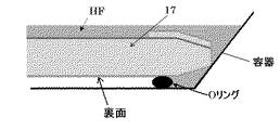
そこで、図2に示すような洗浄装置を用いて、HF水溶液が、ウェーハ表面及び面取り部にのみ行き渡り、裏面側には周り込まないように、裏面外周近傍の周方向全体にリング状のゴム(Oリング)を接触させ、その内側(ウェーハ裏面)をHF水溶液との接触から保護することが好ましい。 Therefore, by using a cleaning apparatus as shown in FIG. 2, a ring-shaped rubber ( It is preferable that the O-ring is contacted and the inner side (wafer back surface) is protected from contact with the HF aqueous solution.
この際、通常の枚葉式スピン方式の片面洗浄機を使用することも可能である。但し、面取り部でのHF水溶液による酸化膜除去を確実にして、再生研磨における面取り部のイオン注入残存層の除去を確実なものとし、更に裏面側のHF水溶液の周り込みの抑制も確実なものとするためには、上述した裏面の周辺部にリング状のゴムを接触させて、HF水溶液の回り込みを防止する機能を有する装置を使用することが望ましい。 At this time, it is possible to use a normal single-wafer type single-sided washer. However, the oxide film removal by the HF aqueous solution at the chamfered portion is ensured, the removal of the ion implantation residual layer at the chamfered portion in the regenerating polishing is ensured, and the HF aqueous solution on the back surface side is also reliably suppressed. In order to achieve this, it is desirable to use an apparatus having a function of preventing the HF aqueous solution from flowing by bringing the ring-shaped rubber into contact with the peripheral portion of the back surface described above.
そして図1(h)に示すように、最後に、もしくは、両面研磨を施した直後に、通常のバッチ式HF液槽浸漬方式のようなHF洗浄を行うことで、裏面の酸化膜12を除去することができ、初期のウェーハと同等の表面及び裏面品質を持つ再生ウェーハを作製することが可能である。
Then, as shown in FIG. 1 (h), the
以上のような本発明により剥離ウェーハを再生加工することで、貼り合わせウェーハの製造における品質向上とコスト低減を効果的に達成できる。 By reclaiming the peeled wafer according to the present invention as described above, quality improvement and cost reduction in the production of bonded wafers can be effectively achieved.
以下、実施例及び比較例を示して本発明をより具体的に説明するが、本発明はこれらに限定されるものではない。
(実施例1)
ボンドウェーハとして、直径300mm、ウェーハ厚さ775μm、COPの無いシリコン単結晶ウェーハを準備した。そのベア面に対し、イオン注入機にて、50KeVの加速電圧でH+イオンを5×10¹⁶atoms/cm2注入した。ベースウェーハには、直径300mm、ウェーハ厚さ775μmのシリコン単結晶ウェーハを用い、145nmの熱酸化膜を形成しておいた。
EXAMPLES Hereinafter, although an Example and a comparative example are shown and this invention is demonstrated more concretely, this invention is not limited to these.
(Example 1)
A silicon single crystal wafer having a diameter of 300 mm, a wafer thickness of 775 μm, and no COP was prepared as a bond wafer. H + ions were implanted into the bare surface at an acceleration voltage of 50 KeV with an ion implanter at 5 × 10 16 atoms / cm 2 . As the base wafer, a silicon single crystal wafer having a diameter of 300 mm and a wafer thickness of 775 μm was used, and a thermal oxide film of 145 nm was formed.
ボンドウェーハの注入面を接合面として、ベースウェーハの熱酸化膜表面に密着させた後、バッチ式横型熱処理炉にて、投入温度200℃、最高温度500℃の熱処理を施し、ボンドウェーハをイオン注入層から剥離して、ベースウェーハ上にSOI層を形成した。
剥離されたボンドウェーハについて、裏面のみにCVDにより酸化膜1μmをデポ形成した。このウェーハを、両面研磨機にて研磨を行った。研磨による表面側の取代は3.0μmとし、この時のウェーハ厚さの変化量も3.0μmとなった。両面研磨後には、面取り部研磨、仕上げ研磨を施した。
After bonding the bond wafer implantation surface to the thermal oxide film surface of the base wafer, heat treatment at a batch temperature of 200 ° C and a maximum temperature of 500 ° C is performed in a batch type horizontal heat treatment furnace to ion-implant the bond wafer. An SOI layer was formed on the base wafer by peeling from the layer.
About the peeled bond wafer, 1 micrometer of oxide films were deposited by CVD only on the back surface. This wafer was polished by a double-side polishing machine. The machining allowance on the surface side by polishing was 3.0 μm, and the amount of change in wafer thickness at this time was also 3.0 μm. After double-side polishing, chamfered portion polishing and finish polishing were performed.
仕上げ研磨後のウェーハ表面パーティクルを、レーザー散乱型パーティクル測定機で測定すると、0.12μmupの粒径でのカウントは1個/枚となった。表面レーザー反射型フラットネス測定機にて、このウェーハのエッジロールオフ量を測定したところ、100nmという値が得られた。静電容量型ウェーハ形状測定機にてウェーハ厚さを測定すると、772μmであった。 When the wafer surface particles after finish polishing were measured with a laser scattering type particle measuring machine, the count with a particle size of 0.12 μmup was 1 / sheet. When the edge roll-off amount of this wafer was measured with a surface laser reflection type flatness measuring device, a value of 100 nm was obtained. When the wafer thickness was measured with a capacitance type wafer shape measuring machine, it was 772 μm.
得られた再生ウェーハに対し、バッチ式HF薬液槽浸漬方式のHF洗浄を施して裏面の酸化膜を除去した後、再度ボンドウェーハとして、上記と同一条件で、酸化、イオン注入、貼り合せ、剥離のSOIウェーハ製造工程を施し、その後、上記と同一条件で再生加工を行った。これを、合計5回繰り返したところ、得られた再生ウェーハでは、パーティクル、エッジロールオフ量は、再生加工1回目と同様の値が得られ、ウェーハ厚さは760μmであった。 The obtained reclaimed wafer is subjected to batch type HF chemical bath immersion method HF cleaning to remove the oxide film on the back surface, and then again as a bond wafer under the same conditions as above, oxidation, ion implantation, bonding, peeling The SOI wafer manufacturing process was applied, and thereafter, reprocessing was performed under the same conditions as described above. When this was repeated a total of 5 times, in the obtained reclaimed wafer, the same particle and edge roll-off values were obtained as in the first reclaim process, and the wafer thickness was 760 μm.
(実施例2)
ボンドウェーハとして、直径300mm、ウェーハ厚さ775μm、COPの無いシリコン単結晶ウェーハを準備し、145nmの熱酸化膜を成長した後、イオン注入機にて、50KeVの加速電圧でH+イオンを5×10¹⁶atoms/cm2注入した。ベースウェーハには、直径300mm、ウェーハ厚さ775μmのシリコン単結晶ウェーハを用い、熱酸化膜は形成しなかった。
(Example 2)
As a bond wafer, a silicon single crystal wafer having a diameter of 300 mm, a wafer thickness of 775 μm, and no COP was prepared. After a thermal oxide film of 145 nm was grown, 5 × H + ions were applied at an acceleration voltage of 50 KeV with an ion implanter. 10 16 atoms / cm 2 was injected. A silicon single crystal wafer having a diameter of 300 mm and a wafer thickness of 775 μm was used as the base wafer, and no thermal oxide film was formed.
注入面を接合面として、ベースウェーハに密着させた後、バッチ式横型熱処理炉にて、投入温度200℃、最高温度500℃の熱処理を施し、ボンドウェーハをイオン注入層から剥離して、ベースウェーハ上にSOI層を形成した。
剥離されたボンドウェーハについて、枚葉HF洗浄機(図2)を使用して表面及び面取り部の酸化膜を除去し、裏面酸化膜はそのまま残存した状態とした。このウェーハを、両面研磨機にて研磨を行った。研磨による表面側の取代は3.0μmとし、この時のウェーハ厚さの変化量も3.0μmとなった。両面研磨後には、面取り部研磨、仕上げ研磨を施した。研磨後のウェーハ表面パーティクルをレーザー散乱型パーティクル測定機で測定すると、0.12μmupの粒径でのカウントは1個/枚となった。表面レーザー反射型フラットネス測定機にて、このウェーハのエッジロールオフ量を測定したところ、100nmという値が得られた。静電容量型ウェーハ形状測定機にてウェーハ厚さを測定すると、772μmであった。
After the implantation surface is brought into close contact with the base wafer, the batch wafer is subjected to a heat treatment at a feeding temperature of 200 ° C. and a maximum temperature of 500 ° C. in a batch type horizontal heat treatment furnace, and the bond wafer is peeled off from the ion implantation layer. An SOI layer was formed thereon.
About the peeled bond wafer, the oxide film of the surface and the chamfered part was removed using the single wafer HF washing machine (FIG. 2), and the back surface oxide film was left as it was. This wafer was polished by a double-side polishing machine. The machining allowance on the surface side by polishing was 3.0 μm, and the amount of change in wafer thickness at this time was also 3.0 μm. After double-side polishing, chamfered portion polishing and finish polishing were performed. When the wafer surface particles after polishing were measured with a laser scattering type particle measuring machine, the count with a particle diameter of 0.12 μmup was 1 / sheet. When the edge roll-off amount of this wafer was measured with a surface laser reflection type flatness measuring device, a value of 100 nm was obtained. When the wafer thickness was measured with a capacitance type wafer shape measuring machine, it was 772 μm.
得られた再生ウェーハに対し、バッチ式HF薬液槽浸漬方式のHF洗浄を施して裏面の酸化膜を除去した後、再度ボンドウェーハとして、上記と同一条件で、酸化、イオン注入、貼り合せ、剥離のSOIウェーハ製造工程を施し、その後、上記と同一条件で再生を行った。これを、合計5回繰り返したところ、得られた再生ウェーハでは、パーティクル、エッジロールオフ量は、再生加工1回目と同様の値が得られ、ウェーハ厚さは760μmであった。 The obtained reclaimed wafer is subjected to batch type HF chemical bath immersion method HF cleaning to remove the oxide film on the back surface, and then again as a bond wafer under the same conditions as above, oxidation, ion implantation, bonding, peeling The SOI wafer manufacturing process was applied, and thereafter, regeneration was performed under the same conditions as described above. When this was repeated a total of 5 times, in the obtained reclaimed wafer, the same particle and edge roll-off values were obtained as in the first reclaim process, and the wafer thickness was 760 μm.
(比較例1)
実施例1,2と同じく、ボンドウェーハとして直径300mm、ウェーハ厚さ775μm、COPの無いシリコン単結晶ウェーハを準備し、実施例2と同一条件にて、酸化、イオン注入、剥離を実施した。
(Comparative Example 1)
As in Examples 1 and 2, a silicon single crystal wafer having a diameter of 300 mm, a wafer thickness of 775 μm, and no COP was prepared as a bond wafer, and oxidation, ion implantation, and peeling were performed under the same conditions as in Example 2.
剥離されたボンドウェーハについて、バッチ式HF薬液槽浸漬方式のHF洗浄を施し、表面、面取り部、及び裏面の酸化膜を除去した。このウェーハを、両面研磨機に投入して研磨を行った。研磨による表面側の取代は3.0μmとし、この時のウェーハ厚さの変化量は6.0μmとなった。両面研磨後には、実施例1,2と同一条件にて、面取り部研磨、仕上げ研磨を施した。研磨後のウェーハ表面パーティクルをレーザー散乱型パーティクル測定機で測定すると、0.12μmupの粒径でのカウントは1個/枚となった。表面レーザー反射型フラットネス測定機にて、このウェーハのエッジロールオフ量を測定したところ、100nmという数字が得られた。静電容量型ウェーハ形状測定機にて、ウェーハ厚さを測定すると、769μmであった。 The peeled bond wafer was subjected to batch-type HF chemical bath immersion type HF cleaning, and the oxide film on the front surface, chamfered portion, and back surface was removed. This wafer was put into a double-side polishing machine and polished. The machining allowance on the surface side by polishing was 3.0 μm, and the amount of change in wafer thickness at this time was 6.0 μm. After double-side polishing, chamfered portion polishing and finish polishing were performed under the same conditions as in Examples 1 and 2. When the wafer surface particles after polishing were measured with a laser scattering type particle measuring machine, the count with a particle diameter of 0.12 μmup was 1 / sheet. When the edge roll-off amount of this wafer was measured with a surface laser reflection type flatness measuring device, a number of 100 nm was obtained. When the wafer thickness was measured with a capacitance-type wafer shape measuring machine, it was 769 μm.
得られた再生ウェーハに対し、通常のバッチ式RCA洗浄を施した後、再度ボンドウェーハとして、上記と同一条件で、酸化、イオン注入、貼り合せ、剥離のSOIウェーハ製造工程を施し、その後、上記と同一条件で再生加工を行った。これを、合計5回繰り返したところ、得られた再生ウェーハでは、パーティクル、エッジロールオフ量は、再生加工1回目と同様の値が得られ、ウェーハ厚さは745μmであった。ウェーハ厚さの規格として775μm±25μmという規格を持つ品種に対して、ウェーハ厚さが不合格となった。 The obtained reclaimed wafer is subjected to normal batch-type RCA cleaning, and again subjected to an SOI wafer manufacturing process of oxidation, ion implantation, bonding, and peeling under the same conditions as described above as a bond wafer. Recycled processing was performed under the same conditions. When this was repeated a total of 5 times, in the obtained reclaimed wafer, the same particle and edge roll-off values were obtained as in the first reclaim process, and the wafer thickness was 745 μm. The wafer thickness was rejected for a product having a standard of 775 μm ± 25 μm as the standard of the wafer thickness.
(比較例2)
実施例1、2、比較例1と同じく、ボンドウェーハとして直径300mm、ウェーハ厚さ775μm、COPの無いシリコン単結晶ウェーハを準備し、実施例2と同一条件にて、酸化、イオン注入、剥離を実施した。
(Comparative Example 2)
As in Examples 1 and 2 and Comparative Example 1, a bond single wafer having a diameter of 300 mm, a wafer thickness of 775 μm, and a COP-free silicon single crystal wafer was prepared. Under the same conditions as in Example 2, oxidation, ion implantation, and peeling were performed. Carried out.
剥離されたボンドウェーハについて、バッチ式HF薬液槽浸漬方式のHF洗浄を施し、表面、面取り部、及び裏面の酸化膜を除去した。このウェーハを、片面研磨機に投入して表面側のみの研磨を行った。研磨による表面側の取代は3.0μmとし、この時のウェーハ厚さの変化量は3.0μmとなった。片面研磨後には、実施例1、2と同一条件にて、面取り部研磨、仕上げ研磨を施した。研磨後のウェーハ表面パーティクルをレーザー散乱型パーティクル測定機で測定すると、0.12μmupの粒径でのカウントは1個/枚となった。表面レーザー反射型フラットネス測定機にて、このウェーハのエッジロールオフ量を測定したところ、420nmという大きな値となった。静電容量型ウェーハ形状測定機にてウェーハ厚さを測定すると、772μmであった。 The peeled bond wafer was subjected to batch-type HF chemical bath immersion type HF cleaning, and the oxide film on the front surface, chamfered portion, and back surface was removed. This wafer was put into a single-side polishing machine to polish only the surface side. The machining allowance on the surface side by polishing was 3.0 μm, and the amount of change in wafer thickness at this time was 3.0 μm. After single-side polishing, chamfered portion polishing and finish polishing were performed under the same conditions as in Examples 1 and 2. When the wafer surface particles after polishing were measured with a laser scattering type particle measuring machine, the count with a particle diameter of 0.12 μmup was 1 / sheet. When the edge roll-off amount of this wafer was measured with a surface laser reflection type flatness measuring device, it was as large as 420 nm. When the wafer thickness was measured with a capacitance type wafer shape measuring machine, it was 772 μm.
得られた再生ウェーハに対し、通常のバッチ式RCA洗浄を施した後、再度ボンドウェーハとして、上記と同一条件で、酸化、イオン注入、貼り合せ、剥離のSOIウェーハ製造工程を施し、その後、上記と同一条件で再生加工を行った。これを、合計5回繰り返したところ、得られた再生ウェーハでは、パーティクルは同様の値が得られたが、エッジロールオフ量は悪化がみられ、485nmという更に大きな値になった。ウェーハ厚さは760μmであった。
エッジロールオフ量の悪化の影響としては、テラス幅の増大がみられた。すなわち、再生加工を5回行った後のウェーハをボンドウェーハとして用いて作製したSOIウェーハに関し、実施例1,2、比較例1では、ノッチ反対側位置で測定したテラス幅は1.2mmであったが、比較例2では2.2mmに広がっているのが確認された。
The obtained reclaimed wafer is subjected to normal batch-type RCA cleaning, and again subjected to an SOI wafer manufacturing process of oxidation, ion implantation, bonding, and peeling under the same conditions as described above as a bond wafer. Recycled processing was performed under the same conditions. When this was repeated a total of 5 times, the same value was obtained for the particles in the obtained reclaimed wafer, but the edge roll-off amount deteriorated and became a larger value of 485 nm. The wafer thickness was 760 μm.
As an influence of the deterioration of the edge roll-off amount, an increase in terrace width was observed. That is, regarding the SOI wafer manufactured using the wafer after the recycle processing was performed five times as the bond wafer, in Examples 1 and 2 and Comparative Example 1, the terrace width measured at the position opposite to the notch was 1.2 mm. However, in Comparative Example 2, it was confirmed that the width was expanded to 2.2 mm.
なお、本発明は、上記実施形態に限定されるものではない。上記実施形態は、例示であり、本発明の特許請求の範囲に記載された技術的思想と実質的に同一な構成を有し、同様な作用効果を奏するものは、いかなるものであっても本発明の技術的範囲に包含される。 The present invention is not limited to the above embodiment. The above-described embodiment is an exemplification, and the present invention has substantially the same configuration as the technical idea described in the claims of the present invention, and any device that exhibits the same function and effect is the present invention. It is included in the technical scope of the invention.
10…ボンドウェーハ、 11…ベースウェーハ、 12…酸化膜、
13…イオン注入層、 14…貼り合わせウェーハ、 15…薄膜、
16…埋め込み酸化膜、 17…剥離ウェーハ、 18…剥離面。
10 ... Bond wafer, 11 ... Base wafer, 12 ... Oxide film,
13 ... ion implantation layer, 14 ... bonded wafer, 15 ... thin film,
16 ... Embedded oxide film, 17 ... Release wafer, 18 ... Release surface.
Claims (2)
前記再生研磨において、前記剥離ウェーハを、該剥離ウェーハの剥離面には酸化膜が形成されておらず、かつ、前記剥離面とは反対の裏面には酸化膜が形成されている状態で、両面研磨機で研磨することにより、前記剥離ウェーハの片面研磨を行うことを特徴とする剥離ウェーハの再生加工方法。 An ion implantation layer is formed by ion implantation of at least one kind of gas ions of hydrogen ions and rare gas ions on the surface of the bond wafer, and the surface of the bond wafer and the surface of the base wafer are directly or oxide film formed. Then, the bonded wafer is peeled off by the ion-implanted layer, so that the peeled wafer produced as a by-product when the bonded wafer having a thin film on the base wafer is produced is regenerated and polished again. In the remanufacturing method for peeled wafers that can be used as bond wafers or base wafers,
In the regenerative polishing, both sides of the release wafer are formed with an oxide film not formed on the release surface of the release wafer and an oxide film formed on the back surface opposite to the release surface. A method for reclaiming a release wafer , wherein the release wafer is polished on one side by polishing with a polishing machine.
The method for reclaiming a peeled wafer according to claim 1, wherein an oxide film other than the oxide film on the back surface of the peeled wafer is removed, and then the reclaiming is performed.
Priority Applications (7)
| Application Number | Priority Date | Filing Date | Title |
|---|---|---|---|
| JP2011227893A JP5799740B2 (en) | 2011-10-17 | 2011-10-17 | Recycled wafer reclaim processing method |
| KR1020147009921A KR101905811B1 (en) | 2011-10-17 | 2012-08-29 | Method for reclaiming peeled-off wafer |
| US14/349,133 US9496130B2 (en) | 2011-10-17 | 2012-08-29 | Reclaiming processing method for delaminated wafer |
| PCT/JP2012/005418 WO2013057865A1 (en) | 2011-10-17 | 2012-08-29 | Method for reclaiming peeled-off wafer |
| EP12840892.9A EP2770524B1 (en) | 2011-10-17 | 2012-08-29 | Method for reclaiming peeled-off wafer |
| CN201280050352.7A CN103875061B (en) | 2011-10-17 | 2012-08-29 | The process for regenerating of removed wafer |
| TW101132517A TWI550702B (en) | 2011-10-17 | 2012-09-06 | Removal of wafer wafer recycling method |
Applications Claiming Priority (1)
| Application Number | Priority Date | Filing Date | Title |
|---|---|---|---|
| JP2011227893A JP5799740B2 (en) | 2011-10-17 | 2011-10-17 | Recycled wafer reclaim processing method |
Publications (3)
| Publication Number | Publication Date |
|---|---|
| JP2013089720A JP2013089720A (en) | 2013-05-13 |
| JP2013089720A5 JP2013089720A5 (en) | 2014-05-15 |
| JP5799740B2 true JP5799740B2 (en) | 2015-10-28 |
Family
ID=48140536
Family Applications (1)
| Application Number | Title | Priority Date | Filing Date |
|---|---|---|---|
| JP2011227893A Active JP5799740B2 (en) | 2011-10-17 | 2011-10-17 | Recycled wafer reclaim processing method |
Country Status (7)
| Country | Link |
|---|---|
| US (1) | US9496130B2 (en) |
| EP (1) | EP2770524B1 (en) |
| JP (1) | JP5799740B2 (en) |
| KR (1) | KR101905811B1 (en) |
| CN (1) | CN103875061B (en) |
| TW (1) | TWI550702B (en) |
| WO (1) | WO2013057865A1 (en) |
Families Citing this family (10)
| Publication number | Priority date | Publication date | Assignee | Title |
|---|---|---|---|---|
| JP5888286B2 (en) * | 2013-06-26 | 2016-03-16 | 信越半導体株式会社 | Manufacturing method of bonded wafer |
| JP6136786B2 (en) * | 2013-09-05 | 2017-05-31 | 信越半導体株式会社 | Manufacturing method of bonded wafer |
| JP6090184B2 (en) * | 2014-01-27 | 2017-03-08 | 信越半導体株式会社 | Semiconductor wafer cleaning tank and bonded wafer manufacturing method |
| CN103794467A (en) * | 2014-02-21 | 2014-05-14 | 上海超硅半导体有限公司 | Recycle method for thin silicon wafers |
| US20180033609A1 (en) * | 2016-07-28 | 2018-02-01 | QMAT, Inc. | Removal of non-cleaved/non-transferred material from donor substrate |
| JP6772820B2 (en) * | 2016-12-22 | 2020-10-21 | 日亜化学工業株式会社 | Manufacturing method of recycled circuit board and manufacturing method of light emitting element |
| JP6607207B2 (en) * | 2017-01-25 | 2019-11-20 | 信越半導体株式会社 | Manufacturing method of bonded SOI wafer |
| CN110620126A (en) * | 2019-09-26 | 2019-12-27 | 德淮半导体有限公司 | Image sensor and method for manufacturing the same |
| CN116941013A (en) * | 2021-03-09 | 2023-10-24 | 东京毅力科创株式会社 | Method for manufacturing laminated substrate and substrate processing apparatus |
| CN113192823B (en) * | 2021-04-27 | 2022-06-21 | 麦斯克电子材料股份有限公司 | Regeneration processing method of substrate slice after SOI bonding process |
Family Cites Families (27)
| Publication number | Priority date | Publication date | Assignee | Title |
|---|---|---|---|---|
| FR2681472B1 (en) | 1991-09-18 | 1993-10-29 | Commissariat Energie Atomique | PROCESS FOR PRODUCING THIN FILMS OF SEMICONDUCTOR MATERIAL. |
| JP3500063B2 (en) * | 1998-04-23 | 2004-02-23 | 信越半導体株式会社 | Method for recycling peeled wafer and silicon wafer for reuse |
| JP3943782B2 (en) * | 1999-11-29 | 2007-07-11 | 信越半導体株式会社 | Reclaimed wafer reclaim processing method and reclaimed peeled wafer |
| US6884696B2 (en) * | 2001-07-17 | 2005-04-26 | Shin-Etsu Handotai Co., Ltd. | Method for producing bonding wafer |
| JP4415588B2 (en) | 2003-08-28 | 2010-02-17 | 株式会社Sumco | Recycled wafer reclaim processing method |
| JP4492054B2 (en) * | 2003-08-28 | 2010-06-30 | 株式会社Sumco | Reclaimed wafer reclaim processing method and reclaimed wafer |
| JP4474863B2 (en) * | 2003-08-28 | 2010-06-09 | 株式会社Sumco | Reclaimed wafer reclaim processing method and reclaimed wafer |
| JP2005079389A (en) * | 2003-09-01 | 2005-03-24 | Sumitomo Mitsubishi Silicon Corp | Method and board for separating laminated wafer |
| JP2005093869A (en) * | 2003-09-19 | 2005-04-07 | Mimasu Semiconductor Industry Co Ltd | Method of regenerating silicon wafer, and regenerated wafer |
| JP4407384B2 (en) | 2004-05-28 | 2010-02-03 | 株式会社Sumco | Manufacturing method of SOI substrate |
| US7402520B2 (en) * | 2004-11-26 | 2008-07-22 | Applied Materials, Inc. | Edge removal of silicon-on-insulator transfer wafer |
| JP2006294737A (en) * | 2005-04-07 | 2006-10-26 | Sumco Corp | Method of manufacturing soi substrate and method of reproducing peeled wafer during manufacture thereof |
| JP4715470B2 (en) | 2005-11-28 | 2011-07-06 | 株式会社Sumco | Release wafer reclaim processing method and release wafer regenerated by this method |
| JP5314838B2 (en) * | 2006-07-14 | 2013-10-16 | 信越半導体株式会社 | Method for reusing peeled wafers |
| FR2928775B1 (en) | 2008-03-11 | 2011-12-09 | Soitec Silicon On Insulator | PROCESS FOR PRODUCING A SEMICONDUCTOR-TYPE SUBSTRATE ON INSULATION |
| JP5654206B2 (en) * | 2008-03-26 | 2015-01-14 | 株式会社半導体エネルギー研究所 | Method for manufacturing SOI substrate and semiconductor device using the SOI substrate |
| EP2105957A3 (en) * | 2008-03-26 | 2011-01-19 | Semiconductor Energy Laboratory Co., Ltd. | Method for manufacturing soi substrate and method for manufacturing semiconductor device |
| JP5446160B2 (en) * | 2008-07-31 | 2014-03-19 | 株式会社Sumco | Manufacturing method of recycled silicon wafer |
| EP2213415A1 (en) * | 2009-01-29 | 2010-08-04 | S.O.I. TEC Silicon | Device for polishing the edge of a semiconductor substrate |
| EP2219208B1 (en) | 2009-02-12 | 2012-08-29 | Soitec | Method for reclaiming a surface of a substrate |
| EP2246882B1 (en) * | 2009-04-29 | 2015-03-04 | Soitec | Method for transferring a layer from a donor substrate onto a handle substrate |
| WO2011043178A1 (en) * | 2009-10-09 | 2011-04-14 | Semiconductor Energy Laboratory Co., Ltd. | Reprocessing method of semiconductor substrate, manufacturing method of reprocessed semiconductor substrate, and manufacturing method of soi substrate |
| FR2953988B1 (en) * | 2009-12-11 | 2012-02-10 | S O I Tec Silicon On Insulator Tech | PROCESS FOR DETOURING A CHANNEL SUBSTRATE |
| JP5643509B2 (en) * | 2009-12-28 | 2014-12-17 | 信越化学工業株式会社 | SOS substrate manufacturing method with reduced stress |
| JP5521561B2 (en) | 2010-01-12 | 2014-06-18 | 信越半導体株式会社 | Manufacturing method of bonded wafer |
| SG173283A1 (en) * | 2010-01-26 | 2011-08-29 | Semiconductor Energy Lab | Method for manufacturing soi substrate |
| US9123529B2 (en) * | 2011-06-21 | 2015-09-01 | Semiconductor Energy Laboratory Co., Ltd. | Method for reprocessing semiconductor substrate, method for manufacturing reprocessed semiconductor substrate, and method for manufacturing SOI substrate |
-
2011
- 2011-10-17 JP JP2011227893A patent/JP5799740B2/en active Active
-
2012
- 2012-08-29 KR KR1020147009921A patent/KR101905811B1/en active IP Right Grant
- 2012-08-29 US US14/349,133 patent/US9496130B2/en active Active
- 2012-08-29 CN CN201280050352.7A patent/CN103875061B/en active Active
- 2012-08-29 WO PCT/JP2012/005418 patent/WO2013057865A1/en active Application Filing
- 2012-08-29 EP EP12840892.9A patent/EP2770524B1/en active Active
- 2012-09-06 TW TW101132517A patent/TWI550702B/en active
Also Published As
| Publication number | Publication date |
|---|---|
| EP2770524B1 (en) | 2017-09-27 |
| KR101905811B1 (en) | 2018-10-08 |
| TW201324603A (en) | 2013-06-16 |
| US9496130B2 (en) | 2016-11-15 |
| KR20140082701A (en) | 2014-07-02 |
| CN103875061B (en) | 2016-07-06 |
| EP2770524A1 (en) | 2014-08-27 |
| US20140273400A1 (en) | 2014-09-18 |
| TWI550702B (en) | 2016-09-21 |
| WO2013057865A1 (en) | 2013-04-25 |
| JP2013089720A (en) | 2013-05-13 |
| EP2770524A4 (en) | 2015-07-22 |
| CN103875061A (en) | 2014-06-18 |
Similar Documents
| Publication | Publication Date | Title |
|---|---|---|
| JP5799740B2 (en) | Recycled wafer reclaim processing method | |
| KR100733113B1 (en) | Method for recycled separated wafer | |
| KR101364008B1 (en) | Method for reusing removed wafer | |
| JP5266496B2 (en) | Chamfer board routing method | |
| US7829436B2 (en) | Process for regeneration of a layer transferred wafer and regenerated layer transferred wafer | |
| WO2013102968A1 (en) | Method for manufacturing bonded silicon-on-insulator (soi) wafer | |
| TWI480939B (en) | Method for reclaiming a surface of a substrate | |
| EP2924736B1 (en) | Method for manufacturing soi wafer | |
| JP5888286B2 (en) | Manufacturing method of bonded wafer | |
| JP2005072073A (en) | Method of regenerating releasable wafer and regenerated wafer | |
| JP4474863B2 (en) | Reclaimed wafer reclaim processing method and reclaimed wafer | |
| JP6136786B2 (en) | Manufacturing method of bonded wafer | |
| JP6607207B2 (en) | Manufacturing method of bonded SOI wafer | |
| EP3029730B1 (en) | Bonded wafer manufacturing method | |
| TW202347607A (en) | Process for fabricating a double semiconductor-on-insulator structure |
Legal Events
| Date | Code | Title | Description |
|---|---|---|---|
| A621 | Written request for application examination |
Free format text: JAPANESE INTERMEDIATE CODE: A621 Effective date: 20130913 |
|
| A521 | Request for written amendment filed |
Free format text: JAPANESE INTERMEDIATE CODE: A523 Effective date: 20140328 |
|
| A131 | Notification of reasons for refusal |
Free format text: JAPANESE INTERMEDIATE CODE: A131 Effective date: 20141104 |
|
| A521 | Request for written amendment filed |
Free format text: JAPANESE INTERMEDIATE CODE: A523 Effective date: 20141209 |
|
| TRDD | Decision of grant or rejection written | ||
| A01 | Written decision to grant a patent or to grant a registration (utility model) |
Free format text: JAPANESE INTERMEDIATE CODE: A01 Effective date: 20150728 |
|
| A61 | First payment of annual fees (during grant procedure) |
Free format text: JAPANESE INTERMEDIATE CODE: A61 Effective date: 20150810 |
|
| R150 | Certificate of patent or registration of utility model |
Ref document number: 5799740 Country of ref document: JP Free format text: JAPANESE INTERMEDIATE CODE: R150 |
|
| S531 | Written request for registration of change of domicile |
Free format text: JAPANESE INTERMEDIATE CODE: R313531 |
|
| R350 | Written notification of registration of transfer |
Free format text: JAPANESE INTERMEDIATE CODE: R350 |
|
| R250 | Receipt of annual fees |
Free format text: JAPANESE INTERMEDIATE CODE: R250 |
|
| R250 | Receipt of annual fees |
Free format text: JAPANESE INTERMEDIATE CODE: R250 |
|
| R250 | Receipt of annual fees |
Free format text: JAPANESE INTERMEDIATE CODE: R250 |
|
| R250 | Receipt of annual fees |
Free format text: JAPANESE INTERMEDIATE CODE: R250 |
|
| R250 | Receipt of annual fees |
Free format text: JAPANESE INTERMEDIATE CODE: R250 |
|
| R250 | Receipt of annual fees |
Free format text: JAPANESE INTERMEDIATE CODE: R250 |