JP5597228B2 - Front-end circuit, impedance adjustment method - Google Patents
Front-end circuit, impedance adjustment method Download PDFInfo
- Publication number
- JP5597228B2 JP5597228B2 JP2012155246A JP2012155246A JP5597228B2 JP 5597228 B2 JP5597228 B2 JP 5597228B2 JP 2012155246 A JP2012155246 A JP 2012155246A JP 2012155246 A JP2012155246 A JP 2012155246A JP 5597228 B2 JP5597228 B2 JP 5597228B2
- Authority
- JP
- Japan
- Prior art keywords
- impedance adjustment
- control signal
- frequency band
- variable impedance
- switch
- Prior art date
- Legal status (The legal status is an assumption and is not a legal conclusion. Google has not performed a legal analysis and makes no representation as to the accuracy of the status listed.)
- Expired - Fee Related
Links
- 238000000034 method Methods 0.000 title claims description 6
- 230000005540 biological transmission Effects 0.000 claims description 42
- 239000000969 carrier Substances 0.000 claims description 11
- 230000007274 generation of a signal involved in cell-cell signaling Effects 0.000 claims description 3
- 238000005259 measurement Methods 0.000 claims description 3
- 230000002776 aggregation Effects 0.000 description 19
- 238000004220 aggregation Methods 0.000 description 19
- 238000010586 diagram Methods 0.000 description 12
- 238000004088 simulation Methods 0.000 description 9
- 238000003780 insertion Methods 0.000 description 3
- 230000037431 insertion Effects 0.000 description 3
- 239000003990 capacitor Substances 0.000 description 1
- 230000002349 favourable effect Effects 0.000 description 1
- 230000010363 phase shift Effects 0.000 description 1
Images


Classifications
-
- H—ELECTRICITY
- H04—ELECTRIC COMMUNICATION TECHNIQUE
- H04L—TRANSMISSION OF DIGITAL INFORMATION, e.g. TELEGRAPHIC COMMUNICATION
- H04L5/00—Arrangements affording multiple use of the transmission path
- H04L5/14—Two-way operation using the same type of signal, i.e. duplex
- H04L5/1461—Suppression of signals in the return path, i.e. bidirectional control circuits
-
- H—ELECTRICITY
- H04—ELECTRIC COMMUNICATION TECHNIQUE
- H04B—TRANSMISSION
- H04B1/00—Details of transmission systems, not covered by a single one of groups H04B3/00 - H04B13/00; Details of transmission systems not characterised by the medium used for transmission
- H04B1/005—Details of transmission systems, not covered by a single one of groups H04B3/00 - H04B13/00; Details of transmission systems not characterised by the medium used for transmission adapting radio receivers, transmitters andtransceivers for operation on two or more bands, i.e. frequency ranges
- H04B1/0053—Details of transmission systems, not covered by a single one of groups H04B3/00 - H04B13/00; Details of transmission systems not characterised by the medium used for transmission adapting radio receivers, transmitters andtransceivers for operation on two or more bands, i.e. frequency ranges with common antenna for more than one band
- H04B1/006—Details of transmission systems, not covered by a single one of groups H04B3/00 - H04B13/00; Details of transmission systems not characterised by the medium used for transmission adapting radio receivers, transmitters andtransceivers for operation on two or more bands, i.e. frequency ranges with common antenna for more than one band using switches for selecting the desired band
-
- H—ELECTRICITY
- H04—ELECTRIC COMMUNICATION TECHNIQUE
- H04B—TRANSMISSION
- H04B1/00—Details of transmission systems, not covered by a single one of groups H04B3/00 - H04B13/00; Details of transmission systems not characterised by the medium used for transmission
- H04B1/38—Transceivers, i.e. devices in which transmitter and receiver form a structural unit and in which at least one part is used for functions of transmitting and receiving
- H04B1/40—Circuits
- H04B1/50—Circuits using different frequencies for the two directions of communication
- H04B1/52—Hybrid arrangements, i.e. arrangements for transition from single-path two-direction transmission to single-direction transmission on each of two paths or vice versa
- H04B1/525—Hybrid arrangements, i.e. arrangements for transition from single-path two-direction transmission to single-direction transmission on each of two paths or vice versa with means for reducing leakage of transmitter signal into the receiver
-
- H—ELECTRICITY
- H04—ELECTRIC COMMUNICATION TECHNIQUE
- H04W—WIRELESS COMMUNICATION NETWORKS
- H04W24/00—Supervisory, monitoring or testing arrangements
- H04W24/08—Testing, supervising or monitoring using real traffic
Landscapes
- Engineering & Computer Science (AREA)
- Signal Processing (AREA)
- Computer Networks & Wireless Communication (AREA)
- Transceivers (AREA)
Description
本発明は携帯端末に用いられるフロントエンド回路、および携帯端末に用いられるフロントエンド回路においてインピーダンスを調整するインピーダンス調整方法に関する。 The present invention relates to a front end circuit used for a mobile terminal and an impedance adjustment method for adjusting impedance in the front end circuit used for the mobile terminal.
昨今、3GPP_Rel.8/9で規格化されたLTE(Long_Term_Evolution)をさらに発展させた規格として、LTE−Advancedが規格化された。LTE−Advancedの仕様の一つにキャリアアグリゲ−ション技術がある。キャリアアグリゲ−ションとは、コンポーネントキャリアと呼ばれる20MHz幅に区分けされた帯域ブロックの搬送波を複数束ねて同時送信・受信する技術である。キャリアアグリゲ−ションには、同一周波数帯域のコンポーネントキャリアを複数束ねて送受信に用いるイントラバンド・キャリアアグリゲーション、異なる周波数帯域のコンポーネントキャリアを複数束ねて送受信に用いるインターバンド・キャリアアグリゲーションがある。 Recently, 3GPP_Rel. LTE-Advanced is standardized as a standard that further develops LTE (Long_Term_Evolution) standardized by 8/9. One of the LTE-Advanced specifications is a carrier aggregation technology. The carrier aggregation is a technology for simultaneously transmitting and receiving a plurality of carrier waves of a band block divided into 20 MHz width called component carriers. Carrier aggregation includes intraband carrier aggregation in which a plurality of component carriers in the same frequency band are bundled for transmission / reception, and interband carrier aggregation in which a plurality of component carriers in different frequency bands are bundled for transmission / reception.
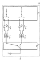
異なる周波数帯域のコンポーネントキャリアを同時に送信・受信する場合、携帯端末のフロントエンド回路には、例えば図1のように異なる周波数帯の搬送波を同時に変調、復調する構成が必要となる。図1はマルチバンド(第1〜第N周波数帯、Nは2以上の整数)での送信・受信を可能にした従来例のフロントエンド回路90の構成を示すブロック図である。図1に示す通り、フロントエンド回路90は、送受共用アンテナ91と、送受共用アンテナ91と共通側接点を接続された2回路N接点のスイッチ92と、スイッチ92のN個の切替側接点のそれぞれに共通端子を接続され第1〜第Nの周波数帯の送信・受信信号が入力されるデュプレクサ93−1〜93−Nと、デュプレクサ93−1〜93−Nの受信端子に接続され第1〜第Nの周波数帯の受信信号を増幅する低雑音増幅器94−1〜94−Nと、デュプレクサ93−1〜93−Nの送信端子に接続され第1〜第Nの周波数帯の送信信号を増幅する増幅器95−1〜95−Nと、第1〜第Nの周波数帯の送信ポートTx1〜TxNと、第1〜第Nの周波数帯の受信ポートRx1〜RxNとを備えるRFIC96を備える。スイッチ92は、基地局から割り当てられたプライマリコンポーネントキャリアと、セカンダリコンポーネントキャリアの二つの周波数帯を同時に使用するため、割り当てられたコンポーネントキャリアに対応する2つのデュプレクサと送受共用アンテナ91とを接続することができる。マルチバンドでの送受信を実現したフロントエンド回路として、例えば特許文献1がある。
When transmitting and receiving component carriers of different frequency bands at the same time, the front end circuit of the mobile terminal needs to have a configuration for simultaneously modulating and demodulating carriers of different frequency bands as shown in FIG. FIG. 1 is a block diagram showing a configuration of a conventional
図1の例において、割り当てられたコンポーネントキャリアの周波数帯がUMTSBand1、Band3であった場合と、UMTSBand1、Band8であった場合について、図2を参照して説明する。図2は、図1に示した従来例のフロントエンド回路90においてキャリアアグリゲ−ションを実行した場合の周波数割り当ての一例を示す図である。図2の例では、第n1番目(n1は1≦n1≦Nを充たす整数)の周波数がUMTS_Band1で固定とし、第n2番目(n2は1≦n2≦Nを充たす整数、n1≠n2)の周波数がUMTS_Band3である場合、UMTS_Band8である場合の2パターンがあるものとする。また、図2の例において、デュプレクサ93−n2は所望の帯域を無損失で通過させ、それ以外の帯域において完全阻止(共通端子の入力インピーダンスが無限大)となる理想的なデュプレクサであるものとし、スイッチ92は理想的なスイッチであるものとする。このときのデュプレクサ93−n1およびデュプレクサ93−n2の通過特性について図3を参照して説明する。図3は、フロントエンド回路90におけるキャリアアグリゲ−ション時のデュプレクサの通過特性のシミュレーション結果を示す図である。図3(a)は、デュプレクサ93−n1の通過特性のシミュレーション結果を示すスミスチャートであって、横軸を50Ωを1として正規化した正規化インピーダンスとする。図3(b)は、デュプレクサ93−n1およびデュプレクサ93−n2(UMTS_Band3)の通過特性のシミュレーション結果を示すグラフであって、横軸が周波数(GHz)、縦軸がSパラメータである。図3(c)は、デュプレクサ93−n1およびデュプレクサ93−n2(UMTS_Band8)の通過特性のシミュレーション結果を示すグラフであって、横軸が周波数(GHz)、縦軸がSパラメータである。図3(b)(c)において、実線−四角形の凡例で示したのはデュプレクサ93−n1の送信側フィルタの通過特性、実線−三角形の凡例で示したのはデュプレクサ93−n1の受信側フィルタの通過特性、点線で示したのはデュプレクサ93−n2の送信側フィルタの通過特性、破線で示したのはデュプレクサ93−n2の受信側フィルタの通過特性である。第n2番目の周波数がUMTS_Band3である場合、図3(b)に点線および破線で示すように、デュプレクサ93−n2(UMTS_Band3)の通過特性は良好で損失が少ない。これは、図3(a)に示すように、UMTS_Band3付近の周波数帯(1.7GHz周辺)において、アンテナ側からみたデュプレクサ93−n1の入力インピーダンスが高くなっているため、UMTS_Band3の送受信信号のデュプレクサ93−n1への回り込みが十分に抑制されるからである。一方、第n2番目の周波数がUMTS_Band8である場合、図3(c)に点線および破線で示すように、デュプレクサ93−n2(UMTS_Band8)の通過特性は損失が大きくなっている。これは、図3(a)に示すように、UMTS_Band8付近の周波数帯(1.0GHz周辺)において、アンテナ側からみたデュプレクサ93−n1の入力インピーダンスが低くなっているため、UMTS_Band8の送受信信号のデュプレクサ93−n1への回り込み(漏洩)が発生してしまうからである。このように、キャリアアグリゲーションにおいては、コンポーネントキャリアの組み合わせによって他の回路のデュプレクサから信号漏洩が発生して挿入損失が増大する場合があり、フロントエンド回路の実装上問題となる。そこで本発明では、キャリアアグリゲーションにおいて複数周波数帯で同時に信号を送受信する場合でも、他の回路への信号漏洩を防ぐことができるフロントエンド回路を提供することを目的とする。
In the example of FIG. 1, the case where the frequency bands of the allocated component carriers are UMTS
本発明のフロントエンド回路は、送受共用アンテナと、送受共用アンテナと共通側接点を接続された2回路N接点(Nは2以上の整数)のスイッチと、アンテナ側端子とRFIC側端子とを備え、スイッチのN個の切替側接点のそれぞれにアンテナ側端子を接続されたN個の可変インピーダンス調整回路と、N個の可変インピーダンス調整回路のRFIC側端子と共通端子とを接続され第1〜第Nの周波数帯の送信・受信信号が入力されるN個のデュプレクサと、制御線によりN個の可変インピーダンス調整回路、およびスイッチと接続され、制御線を介してN個の可変インピーダンス調整回路、およびスイッチの切替制御を実行する制御部と、制御部に制御信号を送信するRFICとを備える。 The front end circuit of the present invention includes a transmission / reception shared antenna, a switch with two circuits and N contacts (N is an integer of 2 or more) connected to the shared transmission / reception antenna, an antenna side terminal and an RFIC side terminal. The N variable impedance adjustment circuits each having an antenna side terminal connected to each of the N switching side contacts of the switch, and the RFIC side terminals and the common terminal of the N variable impedance adjustment circuits are connected to the first to first terminals. N duplexers to which transmission / reception signals of N frequency bands are input, N variable impedance adjustment circuits and switches connected by a control line, and N variable impedance adjustment circuits via the control line, and The control part which performs switching control of a switch, and RFIC which transmits a control signal to a control part are provided.
本発明のフロントエンド回路によれば、キャリアアグリゲーションにおいて複数周波数帯で同時に信号を送受信する場合でも、他の回路への信号漏洩を防ぐことができる。 According to the front end circuit of the present invention, signal leakage to other circuits can be prevented even when signals are simultaneously transmitted and received in a plurality of frequency bands in carrier aggregation.
以下、本発明の実施の形態について、詳細に説明する。なお、同じ機能を有する構成部には同じ番号を付し、重複説明を省略する。 Hereinafter, embodiments of the present invention will be described in detail. In addition, the same number is attached | subjected to the structure part which has the same function, and duplication description is abbreviate | omitted.
前述した従来例のフロントエンド回路90の一部を改良したフロントエンド回路90’について図4を参照して説明する。図4は改良したフロントエンド回路90’においてキャリアアグリゲ−ションを実行した場合の周波数割り当ての一例を示す図である。図4に示す通り、改良したフロントエンド回路90’は、従来の構成に加えて、インピーダンス調整回路97−n1を備える。インピーダンス調整回路97−n1のアンテナ側端子は、スイッチ92の切替側接点の一つと接続され、インピーダンス調整回路97−n1のRFIC側端子は、デュプレクサ93−n1の共通端子と接続されている。第n1番目の周波数がUMTS_Band1で固定とし、第n2番目の周波数がUMTS_Band3である場合、UMTS_Band8である場合の2パターンがある点は図2と同じである。インピーダンス調整回路97−n1は、1GHzの電気長において105°の伝送線路(移相器)であるものとする。このときのデュプレクサ93−n1およびデュプレクサ93−n2の通過特性について図5を参照して説明する。図5は、改良したフロントエンド回路90’におけるキャリアアグリゲ−ション時のデュプレクサの通過特性のシミュレーション結果を示す図である。図5(a)は、デュプレクサ93−n1の通過特性のシミュレーション結果を示すスミスチャートであって、横軸を50Ωを1として正規化した正規化インピーダンスとする。図5(b)は、デュプレクサ93−n1およびデュプレクサ93−n2(UMTS_Band8)の通過特性のシミュレーション結果を示すグラフであって、横軸が周波数(GHz)、縦軸がSパラメータである。前述したとおり、実線−四角形の凡例で示したのはデュプレクサ93−n1の送信側フィルタの通過特性、実線−三角形の凡例で示したのはデュプレクサ93−n1の受信側フィルタの通過特性、点線で示したのはデュプレクサ93−n2の送信側フィルタの通過特性、破線で示したのはデュプレクサ93−n2の受信側フィルタの通過特性である。
A
第n2番目の周波数がUMTS_Band8である場合、図5(b)に点線および破線で示すように、デュプレクサ93−n2(UMTS_Band8)の通過特性は損失が小さくなっている。これは、図5(a)に示すように、UMTS_Band8付近の周波数帯(1.0GHz周辺)において、移相器による位相シフトの影響によりアンテナ側からみたデュプレクサ93−n1の入力インピーダンスが高くなっているため、UMTS_Band8の送受信信号のデュプレクサ93−n1への回り込み(漏洩)が抑止されているからである。図4、図5に示すように、他回路のデュプレクサへの信号漏洩を防止するためにはインピーダンス調整回路が有効であることがわかる。
If the n 2-th frequency is UMTS_Band8, as indicated by a dotted line and a broken line in FIG. 5 (b), pass characteristics of the duplexer 93-n 2 (UMTS_Band8) loss is small. This is because, as shown in FIG. 5 (a), in the frequency band near UMTS_Band8 (1.0GHz) near, high input impedance of the duplexer 93-n 1 viewed from the antenna side due to the influence of the phase shift by the phase shifter This is because wraparound (leakage) of the transmission / reception signal of
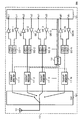
上述の検討を踏まえ、キャリアアグリゲーションにおいて、他の回路への信号漏洩を防ぐ実施例1のフロントエンド回路の概要について図6を参照して説明する。図6は本実施例のフロントエンド回路10の構成を示すブロック図である。図6に示す通り、本実施例のフロントエンド回路10は、送受共用アンテナ91と、送受共用アンテナ91と共通側接点を接続された2回路N接点のスイッチ92と、アンテナ側端子、RFIC側端子を備え、スイッチ92のN個の切替側接点のそれぞれにアンテナ側端子を接続された可変インピーダンス調整回路17−1〜17−Nと、可変インピーダンス調整回路17−1〜17−NのRFIC側端子と共通端子とを接続され第1〜第Nの周波数帯の送信・受信信号が入力されるデュプレクサ93−1〜93−Nと、デュプレクサ93−1〜93−Nの受信端子に接続され第1〜第Nの周波数帯の受信信号を増幅する低雑音増幅器94−1〜94−Nと、デュプレクサ93−1〜93−Nの送信端子に接続され第1〜第Nの周波数帯の送信信号を増幅する増幅器95−1〜95−Nと、第1〜第Nの周波数帯の送信ポートTx1〜TxNと、第1〜第Nの周波数帯の受信ポートRx1〜RxNとを備えるRFIC16と、制御線(図中破線で表示)により可変インピーダンス調整回路17−1〜17−Nと、スイッチ92と接続され、制御線を介して可変インピーダンス調整回路17−1〜17−Nおよびスイッチ92の切替制御を実行する制御部18とを備える。制御部18は、制御信号線(図中白矢印で表示)により、RFIC16に接続されている。制御部18は、制御信号線を介して、RFIC16から制御信号を受信する。本実施例のフロントエンド回路10の可変インピーダンス調整回路17−1〜17−N、制御部18、RFIC16以外の構成については、従来例のフロントエンド回路90における同一番号を付した各構成と同じであるため説明を割愛する。次に、図7を参照して可変インピーダンス調整回路17−n(n=1、2、3、…、N)の構成の一例について説明する。図7は本実施例の可変インピーダンス調整回路17−nの構成例を示すブロック図である。図7に示す通り、本実施例の可変インピーダンス調整回路17−n(n=1、2、3、…、N)は共通の構造を有しており、1回路N+1接点のスイッチ17−n−aと、伝送線路17−n−0と、N個の回路ブロック(回路ブロック17−n−1、回路ブロック17−n−2、…回路ブロック17−n−N)と、1回路N+1接点のスイッチ17−n−bを備える。伝送線路17−n−0、N個の回路ブロックの入出力端子は、スイッチ17−n−a、17−n−bのN+1個の切替側接点のそれぞれと接続されている。伝送線路17−n−0は可能な限り短く構成して、伝送線路17−n−0によるインピーダンス変動がほぼゼロとなるようにする。後に説明する制御信号がインピーダンス調整不要である旨を示す場合には、制御部18はスイッチ17−n−a、17−n−bを切替制御して、回路を伝送線路17−n−0によって導通させ、インピーダンス調整が行われないようにする。回路ブロック17−n−1は第1周波数の送信信号、受信信号をカバーする周波数帯におけるアンテナ側からみた入力インピーダンスが大きくなるように構成された回路ブロックである。同様に、回路ブロック17−n−2、3、4、…、Nは第2、3、4、…、N周波数の送信信号、受信信号をカバーする周波数帯におけるアンテナ側からみた入力インピーダンスが大きくなるように構成された回路ブロックである。回路ブロック17−n−1、2、3、…、Nは例えばインピーダンス調整回路97−n1のような電気長を調整した位相器(伝送線路)であってもよい。本実施例では、スイッチ17−n−a、17−n−bの切替制御によって何れかの回路ブロックが選択されることでチューナブルな可変インピーダンス調整回路17−nを実現したが、これに限られず可変インピーダンス調整回路17−nを容量可変コンデンサ、コイル、伝送線路などを組み合わせてチューナブルとする従来のインピーダンス調整回路を用いて構成してもよい。このように、本実施例の可変インピーダンス調整回路17−nは、第1〜第N周波数帯のいずれかひとつの周波数帯におけるアンテナ側からみた入力インピーダンスを大きくすることができる。ここでインピーダンス調整の目安としては、付加される挿入損失がおよそ1dB以下となることが好ましいことから、キャリアアグリゲ−ションで選択される周波数帯が仮に第p周波数帯、第q周波数帯であったと仮定した場合に(p、qは1≦p、q≦Nを充たす整数、p≠q)、可変インピーダンス調整回路17−pのアンテナ側からみた入力インピーダンスは、第q周波数帯のデュプレクサであるデュプレクサ93−qのアンテナ側からみた入力インピーダンスの4倍以上となるようにすればよい。
Based on the above examination, an outline of the front-end circuit according to the first embodiment that prevents signal leakage to other circuits in carrier aggregation will be described with reference to FIG. FIG. 6 is a block diagram showing the configuration of the front end circuit 10 of this embodiment. As shown in FIG. 6, the front-end circuit 10 of this embodiment includes a transmission / reception shared
なお、図7においては、可変インピーダンス調整回路17−nがN個の周波数帯それぞれに対応するN個の回路ブロックを備えることにより、可変インピーダンス調整回路17−n(n=1、2、3、…、N)を単一の回路構成で共用可能とした。これ以外にも、k番目(kは1≦k≦Nを充たす整数)の周波数帯のデュプレクサ93−kに接続される可変インピーダンス調整回路17−kにおいては、k番目の周波数帯のインピーダンスを調整する回路ブロックが不要であるため、対応する回路ブロックである回路ブロック17−k−kを無くしても良い。この場合、可変インピーダンス調整回路17−nはN−1個の回路ブロックと伝送線路17−n−0により構成される。 In FIG. 7, the variable impedance adjustment circuit 17-n includes N circuit blocks corresponding to the N frequency bands, so that the variable impedance adjustment circuit 17-n (n = 1, 2, 3,. ..., N) can be shared by a single circuit configuration. In addition, in the variable impedance adjustment circuit 17-k connected to the duplexer 93-k in the kth frequency band (k is an integer satisfying 1 ≦ k ≦ N), the impedance of the kth frequency band is adjusted. Therefore, the circuit block 17-k-k, which is a corresponding circuit block, may be eliminated. In this case, the variable impedance adjustment circuit 17-n includes N-1 circuit blocks and the transmission line 17-n-0.
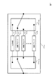
以下、図8、図9を参照して、本実施例のRFIC16が備える制御システムの構成及び動作について説明する。図8は、本実施例のRFIC16が備える制御システムの構成を示すブロック図である。図9は、本実施例のRFIC16が備える制御システムの動作を示すフローチャートである。RFIC16には本実施例の可変インピーダンス調整回路17−1〜17−N、スイッチ92の制御を実行するための制御システムが組み込まれている。制御システムは具体的にはRFIC16内に組み込みソフトウェアとして構成することができる。この組み込みソフトウェアを機能に分けて表現すれば、図8のようになる。図8に示すようにRFIC16内の制御システムは、チャネル品質パラメータ測定部161と、チャネル品質パラメータ送信部162と、割り当てコンポーネントキャリア受信部163と、制御信号生成部164とを備える。チャネル品質パラメータ測定部161は、いずれかのセルに無線リンクを接続した後、このセルからの報知情報を受信、復号し、周辺セル情報を得る。この動作をセルサーチという。チャネル品質パラメータ測定部161は、セルサーチされた全セルのチャネル品質パラメータを測定する(S161)。チャネル品質パラメータ送信部162は、測定されたチャネル品質パラメータを基地局に送信する(S162)。基地局は、チャネル品質パラメータに基づいて、コンポーネントキャリアを決定する。このとき、基地局は一般的には最も受信レベルの大きいコンポーネントキャリアをプライマリコンポーネントキャリア、二番目に受信レベルの大きいコンポーネントキャリアをセカンダリコンポーネントキャリアとして割り当てる。基地局は、携帯端末に対して割り当てたコンポーネントキャリアを報知する情報を送信する。本実施例のRFICが備える割り当てコンポーネントキャリア受信部163は、基地局が割り当てたコンポーネントキャリアの報知情報を受信する(S163)。制御信号生成部164は、受信した割り当てコンポーネントキャリアの報知情報に基づいて、制御信号を生成し、制御部18に送信する。例えば割り当てられたコンポーネントキャリアがプライマリコンポーネントキャリアが第p周波数帯(pは1≦p≦Nを充たす整数)であって、セカンダリコンポーネントキャリアが第q周波数帯(qは1≦q≦Nを充たす整数、p≠q)である場合には、制御信号は第pおよび第q周波数帯に対応する可変インピーダンス調整回路17−p、17−qと接続された切替側接点と共通側接点とを導通させるようにスイッチ92を制御する信号である。また、第p周波数帯に対応する可変インピーダンス調整回路17−pをアンテナ側からみて第q周波数帯の入力インピーダンスが、第q周波数帯のデュプレクサ93−qにおけるインピーダンスよりも大きくなるように調整するものである。また、第q周波数帯に対応する可変インピーダンス調整回路17−qをアンテナ側からみて第p周波数帯の入力インピーダンスが、第p周波数帯のデュプレクサ93−pにおけるインピーダンスよりも大きくなるように調整する制御信号である。前述したように、付加される挿入損失をおよそ1dB以下とするために、可変インピーダンス調整回路のインピーダンスは、対応する周波数帯のデュプレクサのインピーダンスの4倍以上とすることが好ましい。制御部18は制御信号が示す制御内容のとおり、スイッチ92および可変インピーダンス調整回路17−p、17−qの切替制御を実行する。
Hereinafter, the configuration and operation of the control system included in the
このように本実施例のフロントエンド回路10はチューナブル(可変)なインピーダンス調整回路17−1〜17−Nをデュプレクサ93−1〜93−Nの後段に配置し、キャリアアグリゲ−ションにおいて第p、第q周波数帯が選択された場合に、制御部18が第p(q)周波数帯の可変インピーダンス調整回路17−p(q)のアンテナ側からみた入力インピーダンスを第q(p)番目の周波数帯において大きくなるように切替制御するため、他回路への漏洩による信号損失を抑止することができる。
As described above, the front-end circuit 10 according to the present embodiment has the tunable (variable) impedance adjustment circuits 17-1 to 17-N arranged in the subsequent stage of the duplexers 93-1 to 93-N, and is used in carrier aggregation. When the p and qth frequency bands are selected, the
Claims (5)
前記送受共用アンテナと共通側接点を接続された2回路N接点(Nは2以上の整数)のスイッチと、
アンテナ側端子とRFIC側端子とを備え、前記スイッチのN個の切替側接点のそれぞれに前記アンテナ側端子を接続されたN個の可変インピーダンス調整回路と、
前記N個の可変インピーダンス調整回路のRFIC側端子と共通端子とを接続され第1〜第Nの周波数帯の送信・受信信号が入力されるN個のデュプレクサと、
制御線により前記N個の可変インピーダンス調整回路、および前記スイッチと接続され、制御線を介して前記N個の可変インピーダンス調整回路、および前記スイッチの切替制御を実行する制御部と、
前記制御部に制御信号を送信するRFICと、
を備えることを特徴とするフロントエンド回路。 A transmission / reception antenna,
A switch of two circuits N contacts (N is an integer of 2 or more) connected to the common antenna for transmission and reception;
N variable impedance adjustment circuits each having an antenna side terminal and an RFIC side terminal, wherein the antenna side terminal is connected to each of the N switching side contacts of the switch;
N duplexers to which transmission / reception signals in the first to Nth frequency bands are input by connecting the RFIC side terminals and the common terminals of the N variable impedance adjustment circuits;
A control unit which is connected to the N variable impedance adjustment circuits and the switch by a control line, and performs switching control of the N variable impedance adjustment circuits and the switch via the control line;
An RFIC for transmitting a control signal to the control unit;
A front-end circuit comprising:
前記RFICが、
セルサーチを実行し、前記セルサーチされた全セルのチャネル品質パラメータを測定するチャネル品質パラメータ測定部と、
前記測定されたチャネル品質パラメータを基地局に送信するチャネル品質パラメータ送信部と、
前記基地局から割り当てコンポーネントキャリアの報知情報を受信する割り当てコンポーネントキャリア受信部と、
前記受信した割り当てコンポーネントキャリアの報知情報に基づいて、制御信号を生成し、当該生成した制御信号を前記制御部に送信する制御信号生成部と、
を備えることを特徴とするフロントエンド回路。 The front end circuit according to claim 1,
The RFIC is
A channel quality parameter measurement unit that performs a cell search and measures channel quality parameters of all cells subjected to the cell search;
A channel quality parameter transmitter for transmitting the measured channel quality parameter to a base station;
An allocation component carrier receiving unit that receives broadcast information of an allocation component carrier from the base station;
A control signal generating unit that generates a control signal based on the received broadcast information of the allocated component carrier, and transmits the generated control signal to the control unit;
A front-end circuit comprising:
前記制御信号生成部が生成する制御信号は、
前記割り当てられたコンポーネントキャリアが第p周波数帯(pは1≦p≦Nを充たす整数)および第q周波数帯(qは1≦q≦Nを充たす整数、p≠q)である場合に、第pおよび第q周波数帯に対応する可変インピーダンス調整回路と接続された切替側接点と共通側接点とを導通させるように前記スイッチを制御する信号であって、かつ前記第p周波数帯に対応する可変インピーダンス調整回路をアンテナ側からみて第q周波数帯の入力インピーダンスが大きくなるように調整するものであり、前記第q周波数帯に対応する可変インピーダンス調整回路をアンテナ側からみて第p周波数帯の入力インピーダンスが大きくなるように調整する制御信号であること
を特徴とするフロントエンド回路。 A front end circuit according to claim 2,
The control signal generated by the control signal generator is
When the allocated component carriers are the p-th frequency band (p is an integer satisfying 1 ≦ p ≦ N) and the q-th frequency band (q is an integer satisfying 1 ≦ q ≦ N, p ≠ q), A signal for controlling the switch so as to make the switching-side contact and the common-side contact connected to the variable impedance adjustment circuit corresponding to the p and qth frequency bands conductive, and the variable corresponding to the pth frequency band The impedance adjustment circuit is adjusted so that the input impedance in the q-th frequency band is increased when viewed from the antenna side, and the variable impedance adjustment circuit corresponding to the q-th frequency band is viewed from the antenna side as the input impedance in the p-th frequency band. A front-end circuit, characterized in that the control signal is adjusted so as to increase.
前記送受共用アンテナと共通側接点を接続された2回路N接点(Nは2以上の整数)のスイッチと、
アンテナ側端子とRFIC側端子とを備え、前記スイッチのN個の切替側接点のそれぞれに前記アンテナ側端子を接続されたN個の可変インピーダンス調整回路と、
前記N個の可変インピーダンス調整回路のRFIC側端子と共通端子とを接続され第1〜第Nの周波数帯の送信・受信信号が入力されるN個のデュプレクサと、
制御線により前記N個の可変インピーダンス調整回路、および前記スイッチと接続され、制御線を介して前記N個の可変インピーダンス調整回路、および前記スイッチの切替制御を実行する制御部と、
前記制御部に制御信号を送信するRFICと、
を備えるフロントエンド回路においてインピーダンスを調整するインピーダンス調整方法であって、
セルサーチを実行し、前記セルサーチされた全セルのチャネル品質パラメータを測定するチャネル品質パラメータ測定ステップと、
前記測定されたチャネル品質パラメータを基地局に送信するチャネル品質パラメータ送信ステップと、
前記基地局から割り当てコンポーネントキャリアの報知情報を受信する割り当てコンポーネントキャリア受信ステップと、
前記受信した割り当てコンポーネントキャリアの報知情報に基づいて、制御信号を生成し、当該生成した制御信号を前記制御部に送信する制御信号生成ステップと、
を有することを特徴とするインピーダンス調整方法。 A transmission / reception antenna,
A switch of two circuits N contacts (N is an integer of 2 or more) connected to the common antenna for transmission and reception;
N variable impedance adjustment circuits each having an antenna side terminal and an RFIC side terminal, wherein the antenna side terminal is connected to each of the N switching side contacts of the switch;
N duplexers to which transmission / reception signals in the first to Nth frequency bands are input by connecting the RFIC side terminals and the common terminals of the N variable impedance adjustment circuits;
A control unit which is connected to the N variable impedance adjustment circuits and the switch by a control line, and performs switching control of the N variable impedance adjustment circuits and the switch via the control line;
An RFIC for transmitting a control signal to the control unit;
An impedance adjustment method for adjusting impedance in a front-end circuit comprising:
A channel quality parameter measurement step of performing a cell search and measuring channel quality parameters of all cells subjected to the cell search;
A channel quality parameter transmission step of transmitting the measured channel quality parameter to a base station;
An allocation component carrier reception step of receiving broadcast information of an allocation component carrier from the base station;
A control signal generating step of generating a control signal based on the received broadcast information of the allocated component carrier and transmitting the generated control signal to the control unit;
An impedance adjustment method comprising:
前記制御信号生成ステップが生成する制御信号は、
前記割り当てられたコンポーネントキャリアが第p周波数帯(pは1≦p≦Nを充たす整数)および第q周波数帯(qは1≦q≦Nを充たす整数、p≠q)である場合に、第pおよび第q周波数帯に対応する可変インピーダンス調整回路と接続された切替側接点と共通側接点とを導通させるように前記スイッチを制御する信号であって、かつ前記第p周波数に対応する可変インピーダンス調整回路をアンテナ側からみて第q周波数帯の入力インピーダンスが大きくなるように調整するものであり、前記第q周波数帯に対応する可変インピーダンス調整回路をアンテナ側からみて第p周波数帯の入力インピーダンスが大きくなるように調整する制御信号であること
を特徴とするインピーダンス調整方法。 The impedance adjustment method according to claim 4,
The control signal generated by the control signal generation step is
When the allocated component carriers are the p-th frequency band (p is an integer satisfying 1 ≦ p ≦ N) and the q-th frequency band (q is an integer satisfying 1 ≦ q ≦ N, p ≠ q), a variable impedance corresponding to the p-th frequency, and a signal for controlling the switch so that the switching-side contact and the common-side contact connected to the variable impedance adjustment circuit corresponding to the p and q-th frequency bands are conducted. The adjustment circuit is adjusted so that the input impedance of the q-th frequency band is increased when viewed from the antenna side, and the input impedance of the p-th frequency band when the variable impedance adjustment circuit corresponding to the q-th frequency band is viewed from the antenna side. An impedance adjustment method, wherein the control signal is adjusted so as to increase.
Priority Applications (5)
| Application Number | Priority Date | Filing Date | Title |
|---|---|---|---|
| JP2012155246A JP5597228B2 (en) | 2012-07-11 | 2012-07-11 | Front-end circuit, impedance adjustment method |
| CN201380003285.8A CN103843257B (en) | 2012-07-11 | 2013-07-09 | Front-end circuit, impedance adjustment method |
| US14/359,240 US9337990B2 (en) | 2012-07-11 | 2013-07-09 | Front-end circuit and impedance adjustment method |
| PCT/JP2013/068703 WO2014010575A1 (en) | 2012-07-11 | 2013-07-09 | Front-end circuit, impedance adjustment method |
| EP13817551.8A EP2736175B1 (en) | 2012-07-11 | 2013-07-09 | Front-end circuit, impedance adjustment method |
Applications Claiming Priority (1)
| Application Number | Priority Date | Filing Date | Title |
|---|---|---|---|
| JP2012155246A JP5597228B2 (en) | 2012-07-11 | 2012-07-11 | Front-end circuit, impedance adjustment method |
Publications (2)
| Publication Number | Publication Date |
|---|---|
| JP2014017750A JP2014017750A (en) | 2014-01-30 |
| JP5597228B2 true JP5597228B2 (en) | 2014-10-01 |
Family
ID=49916027
Family Applications (1)
| Application Number | Title | Priority Date | Filing Date |
|---|---|---|---|
| JP2012155246A Expired - Fee Related JP5597228B2 (en) | 2012-07-11 | 2012-07-11 | Front-end circuit, impedance adjustment method |
Country Status (5)
| Country | Link |
|---|---|
| US (1) | US9337990B2 (en) |
| EP (1) | EP2736175B1 (en) |
| JP (1) | JP5597228B2 (en) |
| CN (1) | CN103843257B (en) |
| WO (1) | WO2014010575A1 (en) |
Families Citing this family (43)
| Publication number | Priority date | Publication date | Assignee | Title |
|---|---|---|---|---|
| JP5668029B2 (en) * | 2012-07-17 | 2015-02-12 | 株式会社Nttドコモ | Radio circuit, frequency pair determination method |
| JP6330357B2 (en) * | 2014-02-12 | 2018-05-30 | 富士通株式会社 | Antenna device |
| DE112014006466T5 (en) | 2014-03-14 | 2016-12-01 | Epcos Ag | Front end module for carrier aggregation mode |
| GB2526197B (en) * | 2014-04-11 | 2020-11-18 | Skyworks Solutions Inc | Circuits and methods related to radio-frequency receivers having carrier aggregation |
| CN104135300B (en) * | 2014-08-07 | 2017-04-12 | 上海无线电设备研究所 | Ku-waveband multi-channel switching receiving device and switching receiving method |
| GB2536085B (en) * | 2014-10-31 | 2019-10-23 | Skyworks Solutions Inc | A receiving system |
| GB2536088B (en) * | 2014-10-31 | 2019-10-23 | Skyworks Solutions Inc | A receiving system |
| GB2536087B (en) * | 2014-10-31 | 2020-02-12 | Skyworks Solutions Inc | A receiving system |
| DE102015220967B4 (en) * | 2014-10-31 | 2022-08-11 | Skyworks Solutions, Inc. | Diversity receiver in a front-end system with switch network |
| US9385765B2 (en) | 2014-10-31 | 2016-07-05 | Skyworks Solutions, Inc. | Diversity receiver front end system with phase-shifting components |
| JP6181731B2 (en) * | 2014-10-31 | 2017-08-16 | スカイワークス ソリューションズ,インコーポレイテッドSkyworks Solutions,Inc. | Diversity receiver front-end system with switching network |
| US9485001B2 (en) | 2014-10-31 | 2016-11-01 | Skyworks Solutions, Inc. | Diversity receiver front end system with switching network |
| JP6029728B2 (en) * | 2014-10-31 | 2016-11-24 | スカイワークス ソリューションズ,インコーポレイテッドSkyworks Solutions,Inc. | Diversity receiver front-end system with phase shift components |
| US9893752B2 (en) | 2014-10-31 | 2018-02-13 | Skyworks Solutions, Inc. | Diversity receiver front end system with variable-gain amplifiers |
| US10050694B2 (en) | 2014-10-31 | 2018-08-14 | Skyworks Solution, Inc. | Diversity receiver front end system with post-amplifier filters |
| US20160233915A1 (en) * | 2015-02-10 | 2016-08-11 | Mediatek Inc. | Communication device and electronic device |
| CN106299682A (en) * | 2015-05-26 | 2017-01-04 | 西安中兴新软件有限责任公司 | A kind of antenna assembly and control method thereof |
| US9838056B2 (en) | 2015-05-28 | 2017-12-05 | Skyworks Solutions, Inc. | Integrous signal combiner |
| GB2562823A (en) * | 2015-06-01 | 2018-11-28 | Skyworks Solutions Inc | Systems, devices and methods related to diversity receivers |
| CN107710629B (en) * | 2015-07-06 | 2019-09-27 | 株式会社村田制作所 | High-frequency model |
| US9941582B2 (en) | 2015-08-10 | 2018-04-10 | Murata Manufacturing Co., Ltd. | Switch module, front-end module, and driving method for switch module |
| JP6460046B2 (en) | 2015-08-10 | 2019-01-30 | 株式会社村田製作所 | Switch module, front end module, and drive method of switch module |
| US9525447B1 (en) * | 2015-09-18 | 2016-12-20 | Broadcom Corporation | Radio receiver co-existence |
| JP6416067B2 (en) * | 2015-09-24 | 2018-10-31 | 太陽誘電株式会社 | module |
| JP6322174B2 (en) | 2015-09-24 | 2018-05-09 | 太陽誘電株式会社 | module |
| CN106856513B (en) * | 2015-12-07 | 2019-08-06 | 小米科技有限责任公司 | A kind of terminal with communication function |
| EP3182603A1 (en) * | 2015-12-18 | 2017-06-21 | Nokia Technologies Oy | An apparatus and/or method for controlling an impedance coupled to an antenna |
| CN108781065B (en) * | 2016-03-08 | 2022-05-17 | 株式会社村田制作所 | Elastic wave device |
| JP6411398B2 (en) | 2016-03-14 | 2018-10-24 | 太陽誘電株式会社 | Filter circuit, front-end circuit and module |
| KR102076960B1 (en) * | 2016-03-31 | 2020-02-13 | 가부시키가이샤 무라타 세이사쿠쇼 | Complex filter units, high frequency front end circuits and communication devices |
| US9979379B2 (en) | 2016-07-13 | 2018-05-22 | Murata Manufacturing Co., Ltd. | Multiplexer, radio frequency front-end circuit, communication device, and multiplexer design method |
| CN106301462B (en) * | 2016-08-02 | 2017-08-25 | 广东欧珀移动通信有限公司 | Radio frequency control circuit and mobile terminal |
| JP2018098578A (en) * | 2016-12-09 | 2018-06-21 | 株式会社村田製作所 | Communication module |
| CN107493114A (en) * | 2017-07-25 | 2017-12-19 | 广东欧珀移动通信有限公司 | Radio circuit, antenna assembly and electronic equipment |
| CN107332573B (en) | 2017-07-25 | 2021-04-13 | Oppo广东移动通信有限公司 | Radio frequency circuit, antenna device and electronic equipment |
| WO2019031307A1 (en) * | 2017-08-10 | 2019-02-14 | 株式会社村田製作所 | Front-end module and communication device |
| KR102356971B1 (en) * | 2017-10-18 | 2022-01-28 | 삼성전자주식회사 | Method for data transmissions using carrier aggregation and electronic device thereof |
| WO2019176551A1 (en) | 2018-03-15 | 2019-09-19 | 株式会社村田製作所 | Antenna device |
| WO2019187744A1 (en) * | 2018-03-30 | 2019-10-03 | 株式会社村田製作所 | High-frequency module |
| CN112088494A (en) * | 2018-06-28 | 2020-12-15 | 株式会社村田制作所 | High-frequency module and communication device |
| CN110830055B (en) * | 2019-10-30 | 2021-11-16 | 西安广和通无线通信有限公司 | Antenna module and antenna adapting method |
| US11424783B2 (en) | 2019-12-27 | 2022-08-23 | Mediatek Inc. | Transceiver having radio-frequency front-end circuit, dedicated radio-frequency front-end circuit, and switchable matching circuit integrated in same chip |
| TWI756702B (en) * | 2020-06-02 | 2022-03-01 | 立積電子股份有限公司 | Switching circuit |
Family Cites Families (17)
| Publication number | Priority date | Publication date | Assignee | Title |
|---|---|---|---|---|
| CA2327761A1 (en) * | 1999-12-21 | 2001-06-21 | Lucent Technologies Inc. | Wireless systems combining arrangement and method thereof |
| JP3747010B2 (en) * | 2002-04-16 | 2006-02-22 | 埼玉日本電気株式会社 | Portable radio |
| US7076216B2 (en) * | 2002-09-17 | 2006-07-11 | Hitachi Metals, Ltd. | High-frequency device, high-frequency module and communications device comprising them |
| CN100547941C (en) * | 2003-12-11 | 2009-10-07 | 日立金属株式会社 | Multiband high-frequency circuit, multiband high frequency circuit components and multi-band communication apparatus |
| JP4447416B2 (en) * | 2004-09-22 | 2010-04-07 | 株式会社エヌ・ティ・ティ・ドコモ | Multiband mobile communication system and transmitter |
| JP2006148385A (en) * | 2004-11-18 | 2006-06-08 | Hitachi Kokusai Electric Inc | Antenna multiplexer |
| EP1755230B1 (en) * | 2005-08-17 | 2017-03-01 | Samsung Electronics Co., Ltd. | Multi-mode/multi-band wireless transceiver |
| JP4812479B2 (en) * | 2006-03-20 | 2011-11-09 | 株式会社エヌ・ティ・ティ・ドコモ | Mobile station and peripheral cell measurement method |
| WO2008084938A1 (en) * | 2007-01-12 | 2008-07-17 | Electronics And Telecommunications Research Institute | A method of reporting measurement information in packet based cellular system |
| CN101414844A (en) * | 2007-10-19 | 2009-04-22 | 信和控股有限公司 | Two-way signal amplifying device, receiving/transmitting device and signal transmission method |
| CN201114016Y (en) * | 2007-10-19 | 2008-09-10 | 信和控股有限公司 | Two-way signal amplifying device, receiving/emitting set |
| DE102009004720B4 (en) * | 2009-01-15 | 2017-07-27 | Qualcomm Technologies, Inc. (N.D.Ges.D. Staates Delaware) | Multiband impedance matching circuit for adapting planar antennas |
| WO2010137405A1 (en) * | 2009-05-27 | 2010-12-02 | 株式会社村田製作所 | High frequency module |
| JP5075189B2 (en) * | 2009-12-03 | 2012-11-14 | 株式会社エヌ・ティ・ティ・ドコモ | Wireless communication terminal |
| JP2011182271A (en) * | 2010-03-03 | 2011-09-15 | Nec Corp | Radio transmission circuit, radio communication device, and method of configuring radio transmission circuit used therefor |
| JP2012044436A (en) * | 2010-08-19 | 2012-03-01 | Ntt Docomo Inc | Multiband matching circuit |
| JP2012138651A (en) * | 2010-12-24 | 2012-07-19 | Hitachi Media Electoronics Co Ltd | Mobile communication terminal module and mobile communication terminal |
-
2012
- 2012-07-11 JP JP2012155246A patent/JP5597228B2/en not_active Expired - Fee Related
-
2013
- 2013-07-09 US US14/359,240 patent/US9337990B2/en active Active
- 2013-07-09 CN CN201380003285.8A patent/CN103843257B/en not_active Expired - Fee Related
- 2013-07-09 WO PCT/JP2013/068703 patent/WO2014010575A1/en active Application Filing
- 2013-07-09 EP EP13817551.8A patent/EP2736175B1/en not_active Not-in-force
Also Published As
| Publication number | Publication date |
|---|---|
| EP2736175A1 (en) | 2014-05-28 |
| JP2014017750A (en) | 2014-01-30 |
| US20140321312A1 (en) | 2014-10-30 |
| EP2736175A4 (en) | 2015-06-10 |
| CN103843257A (en) | 2014-06-04 |
| CN103843257B (en) | 2015-05-06 |
| WO2014010575A1 (en) | 2014-01-16 |
| EP2736175B1 (en) | 2018-04-04 |
| US9337990B2 (en) | 2016-05-10 |
Similar Documents
| Publication | Publication Date | Title |
|---|---|---|
| JP5597228B2 (en) | Front-end circuit, impedance adjustment method | |
| US9288031B2 (en) | Switch arrangement | |
| US20180138927A1 (en) | Front-end module | |
| CN110235362B (en) | Techniques for low-loss multi-band multiplexing | |
| US20120243446A1 (en) | Multi-band wireless communication device with multiplexer and method of multiplexing multi-band wireless signals | |
| US10277287B2 (en) | Antenna system and harmonic suppression element | |
| US10027006B2 (en) | Integrated multi-band bandpass multiplexer based on dielectric resonators | |
| JP5668029B2 (en) | Radio circuit, frequency pair determination method | |
| US9559746B2 (en) | Systems and methods for multi-channel transceiver communications | |
| US11043930B2 (en) | Radio frequency circuit, radio frequency front end circuit, and communication apparatus | |
| US11296730B2 (en) | Radio-frequency front-end circuit | |
| US20230065202A1 (en) | Remote compensators for mobile devices | |
| CN112425082B (en) | Adjustable antenna and communication terminal | |
| US10530415B2 (en) | HF circuit and front-end circuit comprising an HF circuit | |
| WO2014002703A1 (en) | Mobile communication terminal | |
| US20170331512A1 (en) | High-frequency switch module | |
| WO2013123522A1 (en) | Systems and methods for multi-channel transceiver communications | |
| WO2021226086A1 (en) | Ultra-small millimeter wave 5g beam former architecture | |
| CN110620591A (en) | Frequency band splitter | |
| CN113114299B (en) | Radio frequency structure and electronic equipment | |
| KR20140128014A (en) | Mobile terminal for reducing an insertion loss | |
| JP2014120842A (en) | Front end circuit | |
| CN113452396B (en) | Radio frequency front-end circuit and electronic equipment | |
| CN115250130B (en) | Radio frequency PA Mid device, radio frequency receiving and transmitting system and communication equipment | |
| US11979184B2 (en) | Radio-frequency signal transmitting/receiving circuit |
Legal Events
| Date | Code | Title | Description |
|---|---|---|---|
| A621 | Written request for application examination |
Free format text: JAPANESE INTERMEDIATE CODE: A621 Effective date: 20140225 |
|
| TRDD | Decision of grant or rejection written | ||
| A01 | Written decision to grant a patent or to grant a registration (utility model) |
Free format text: JAPANESE INTERMEDIATE CODE: A01 Effective date: 20140805 |
|
| A61 | First payment of annual fees (during grant procedure) |
Free format text: JAPANESE INTERMEDIATE CODE: A61 Effective date: 20140808 |
|
| R150 | Certificate of patent or registration of utility model |
Ref document number: 5597228 Country of ref document: JP Free format text: JAPANESE INTERMEDIATE CODE: R150 |
|
| R250 | Receipt of annual fees |
Free format text: JAPANESE INTERMEDIATE CODE: R250 |
|
| R250 | Receipt of annual fees |
Free format text: JAPANESE INTERMEDIATE CODE: R250 |
|
| R250 | Receipt of annual fees |
Free format text: JAPANESE INTERMEDIATE CODE: R250 |
|
| R250 | Receipt of annual fees |
Free format text: JAPANESE INTERMEDIATE CODE: R250 |
|
| R250 | Receipt of annual fees |
Free format text: JAPANESE INTERMEDIATE CODE: R250 |
|
| R250 | Receipt of annual fees |
Free format text: JAPANESE INTERMEDIATE CODE: R250 |
|
| LAPS | Cancellation because of no payment of annual fees |