JP5568019B2 - Devices, systems, and methods for frequency generation using atomic resonators - Google Patents
Devices, systems, and methods for frequency generation using atomic resonators Download PDFInfo
- Publication number
- JP5568019B2 JP5568019B2 JP2010545606A JP2010545606A JP5568019B2 JP 5568019 B2 JP5568019 B2 JP 5568019B2 JP 2010545606 A JP2010545606 A JP 2010545606A JP 2010545606 A JP2010545606 A JP 2010545606A JP 5568019 B2 JP5568019 B2 JP 5568019B2
- Authority
- JP
- Japan
- Prior art keywords
- frequency signal
- frequency
- solid
- atomic
- clock
- Prior art date
- Legal status (The legal status is an assumption and is not a legal conclusion. Google has not performed a legal analysis and makes no representation as to the accuracy of the status listed.)
- Expired - Fee Related
Links
Images


Classifications
-
- H—ELECTRICITY
- H03—ELECTRONIC CIRCUITRY
- H03B—GENERATION OF OSCILLATIONS, DIRECTLY OR BY FREQUENCY-CHANGING, BY CIRCUITS EMPLOYING ACTIVE ELEMENTS WHICH OPERATE IN A NON-SWITCHING MANNER; GENERATION OF NOISE BY SUCH CIRCUITS
- H03B17/00—Generation of oscillations using radiation source and detector, e.g. with interposed variable obturator
-
- G—PHYSICS
- G04—HOROLOGY
- G04F—TIME-INTERVAL MEASURING
- G04F5/00—Apparatus for producing preselected time intervals for use as timing standards
- G04F5/14—Apparatus for producing preselected time intervals for use as timing standards using atomic clocks
-
- G—PHYSICS
- G04—HOROLOGY
- G04F—TIME-INTERVAL MEASURING
- G04F5/00—Apparatus for producing preselected time intervals for use as timing standards
- G04F5/14—Apparatus for producing preselected time intervals for use as timing standards using atomic clocks
- G04F5/145—Apparatus for producing preselected time intervals for use as timing standards using atomic clocks using Coherent Population Trapping
-
- H—ELECTRICITY
- H03—ELECTRONIC CIRCUITRY
- H03B—GENERATION OF OSCILLATIONS, DIRECTLY OR BY FREQUENCY-CHANGING, BY CIRCUITS EMPLOYING ACTIVE ELEMENTS WHICH OPERATE IN A NON-SWITCHING MANNER; GENERATION OF NOISE BY SUCH CIRCUITS
- H03B19/00—Generation of oscillations by non-regenerative frequency multiplication or division of a signal from a separate source
-
- H—ELECTRICITY
- H03—ELECTRONIC CIRCUITRY
- H03L—AUTOMATIC CONTROL, STARTING, SYNCHRONISATION, OR STABILISATION OF GENERATORS OF ELECTRONIC OSCILLATIONS OR PULSES
- H03L7/00—Automatic control of frequency or phase; Synchronisation
- H03L7/26—Automatic control of frequency or phase; Synchronisation using energy levels of molecules, atoms, or subatomic particles as a frequency reference
Landscapes
- Physics & Mathematics (AREA)
- General Physics & Mathematics (AREA)
- Spectroscopy & Molecular Physics (AREA)
- Life Sciences & Earth Sciences (AREA)
- Ecology (AREA)
- Stabilization Of Oscillater, Synchronisation, Frequency Synthesizers (AREA)
- Optical Modulation, Optical Deflection, Nonlinear Optics, Optical Demodulation, Optical Logic Elements (AREA)
Description
一部の実施形態は、一般に、周波数発発生の分野に関し、より詳細には、原子共振器を使用した周波数発生に関する。 Some embodiments relate generally to the field of frequency generation, and more particularly to frequency generation using atomic resonators.
今日、ハイエンド周波数標準基準は、比較的コストが高く、サイズが大きく、電力消費が高いなどである。非常に高い変調周波数を使用する、限定はしないが、全地球測位システム(global positioning system)(GPS)および/または可搬型GPSシステム、携帯電話システムおよび/または可搬型携帯電話および/またはサイズが小さくコストが低い携帯電話基地局、高速電気通信システム、ならびに他の高速通信リンクなどのデバイスおよび/またはシステムの急速な展開は、サイズが小さく、コストが低く、電力消費が低い、安定し、精密で、正確な周波数標準基準を必要とする。これらの問題の関するさらなる情報は、その全体の開示が、参照により本明細書に組込まれる、以下の参考文献、M.A.Sturza著「GPS navigation Using Three Satellites and a Precise Clock」Global Positioning System, VOL.2.Washigton,DC:Institute of Navigation,1984,pp.122−132、J.MurphyおよびT.Skidmore著「A low−cost atomic clock:impact on the national airspace and GNSS availability」Proceedings of ION GPS−94;7th International Meeting of the Satellite Division of the institute of Navigation.Salt lake City,UT,1994,pp.1329−1336、H.Fruehauf著「Fast「direct−P(Y)」GPS signal acquision using a special portable clock」33rd Annual Precise Time and Time Interval(PTTI)Meeting.Long Beach,CA,2001,pp.359−369、および/または、J.A.KustersおよびC.A.Adams著「Performance requirements of communication base station time standardas」RF design,28−38(1999)に見出されうる。 Today, high-end frequency standards are relatively expensive, large in size, and high in power consumption. Use very high modulation frequencies, including but not limited to global positioning system (GPS) and / or portable GPS systems, cell phone systems and / or portable cell phones and / or small in size Rapid deployment of devices and / or systems such as low cost mobile phone base stations, high speed telecommunication systems, and other high speed communication links is small, low cost, low power consumption, stable and precise Need accurate frequency standard reference. Further information on these issues can be found in the following references, M. M., the entire disclosure of which is hereby incorporated by reference. A. Sturza, “GPS navigation Using Three Satellites and a Precision Clock”, Global Positioning System, VOL. 2. Washington, DC: Institute of Navigation, 1984, pp. 122-132, J.A. Murphy and T.W. Skidmore, “A low-cost atomic clock: impact on the national airspace and GNSS availability of the ion of the it's the best of the world.” 7th International Meeting of the world. Salt lake City, UT, 1994, pp. 1329-1336, H.M. Fruhauf “Fast“ direct-P (Y) ”GPS signal acquisition using a special portable clock, 33rd Annual Precision Time and Time Interval (PTTI) Meeting. Long Beach, CA, 2001, pp. 359-369, and / or J.I. A. Kusters and C.I. A. Adams, “Performance requirements of communication base station time standard”, RF design, 28-38 (1999).
石英結晶発振器は、一方では、最も一般的に使用されるローカル周波数標準であるが、多くの場合、十分に正確でなく、長期周波数ドリフト、大きなサイズおよび高い電力消費ならびに比較的高いコストを有し、高性能石英結晶発振器の場合、これらの欠点が、石英結晶発振器を上記用途に適さなくさせる。 Quartz crystal oscillators, on the one hand, are the most commonly used local frequency standards, but are often not accurate enough and have long-term frequency drift, large size and high power consumption and relatively high cost In the case of high performance quartz crystal oscillators, these drawbacks make quartz crystal oscillators unsuitable for the above applications.
他方、ルビジウム(Rb)またはセシウム(Cs)ガスベースの原子クロックは、非常に正確であり、また、高い長期周波数安定性を有する。しかし、ガスベースの原子クロックは、サイズが大きく、電力消費が高く、製造コストが高い。 On the other hand, atomic clocks based on rubidium (Rb) or cesium (Cs) gas are very accurate and have high long-term frequency stability. However, gas-based atomic clocks are large in size, high power consumption, and high manufacturing costs.
US特許7142066は、超微細遷移を示すことが可能な実質的に単離された粒子を含む原子クロックを記載する。クロックのアライメントデバイスは、粒子のスピンの支配的な方向を確立する可能性がある。クロックは、粒子を励起することによって、一定時間間隔で粒子に超微細遷移を受けさせる励起デバイスを含んでもよい。クロックの検出デバイスは、粒子の超微細遷移を検出してもよい。US特許7030704は、固体内の常磁性イオンの超微細スペクトルから基準周波数を導出する周波数標準を記載する。 US Pat. No. 7,142,066 describes an atomic clock comprising substantially isolated particles capable of exhibiting hyperfine transitions. Clock alignment devices may establish the dominant direction of particle spin. The clock may include an excitation device that causes the particles to undergo hyperfine transitions at regular time intervals by exciting the particles. The clock detection device may detect a hyperfine transition of particles. US patent 7030704 describes a frequency standard that derives a reference frequency from the hyperfine spectrum of paramagnetic ions in a solid.
一部の実施形態は、たとえば、固体原子共振器を使用した周波数発生のためのデバイス、システム、および方法を含む。 Some embodiments include devices, systems, and methods for frequency generation using, for example, solid atomic resonators.
一部の実施形態では、デバイスは、固体原子共振器モジュールによって提供される入力信号に従って、制御発振器を制御するための信号を提供するフィードバックと、入力信号に従って周波数逓倍器に対して出力周波数を生成する制御発振器と、入力信号の周波数に関連する周波数を有する出力マイクロ波信号を生成する周波数逓倍器と、超微細遷移を示すことが可能な色中心を有する固体原子共振器モジュールとを含み、固体原子共振器モジュールは、周波数逓倍器からマイクロ波信号を受信し、マイクロ波信号の周波数と色中心の超微細共振周波数の周波数との周波数差に関連する出力信号を生成し、出力周波数はマイクロ波信号の周波数に関連する。 In some embodiments, the device generates an output frequency for the frequency multiplier according to the input signal and feedback that provides a signal to control the controlled oscillator according to the input signal provided by the solid atomic resonator module. A controlled oscillator, a frequency multiplier for generating an output microwave signal having a frequency related to the frequency of the input signal, and a solid state atomic resonator module having a color center capable of exhibiting a hyperfine transition, The atomic resonator module receives the microwave signal from the frequency multiplier and generates an output signal related to the frequency difference between the frequency of the microwave signal and the frequency of the hyperfine resonance frequency at the color center, and the output frequency is the microwave Related to the frequency of the signal.
一部の実施形態では、固体原子共振器は、偏光コントローラに光を照射する光源と、光がそこを通り、光減衰器に光を照射する偏光コントローラと、光がそこを通り、光フィルタに光を照射する光減衰器と、光がそこを通り、光中心と相互作用し、かつ、固体原子共振器に光を照射する光フィルタと、光がそこを通り、光フィルタに光を照射する固体原子共振器と、光がそこを通り、原子共振器モジュールの出力信号を生成する光検出器に光を照射する光フィルタと、原子共振器を取り囲む光キャビティと、原子共振器を取り囲むマイクロ波キャビティと、入力マイクロ波信号を受信し、固体原子共振器上に出力マイクロ波電磁波を送信するマイクロ波要素と、原子共振器を取り囲む磁気シールドとを含む。 In some embodiments, the solid state resonator includes a light source that illuminates a polarization controller, a polarization controller that illuminates light and illuminates an optical attenuator, and a light that passes therethrough and into an optical filter. An optical attenuator that irradiates light, an optical filter through which light passes through and interacts with the optical center, and irradiates light to the solid atomic resonator, and light passes through the optical filter and irradiates the optical filter A solid atomic resonator, an optical filter through which light passes and irradiates a photodetector that generates an output signal of the atomic resonator module, an optical cavity that surrounds the atomic resonator, and a microwave that surrounds the atomic resonator A cavity, a microwave element that receives an input microwave signal and transmits an output microwave electromagnetic wave on a solid atomic resonator, and a magnetic shield that surrounds the atomic resonator.
一部の実施形態では、色中心は、ダイアモンド内の窒素−空孔色中心である。 In some embodiments, the color center is a nitrogen-hole color center within the diamond.
一部の実施形態では、固体原子共振器は、窒素−空孔色中心によって埋め込まれたダイアモンド結晶を含む。 In some embodiments, the solid atomic resonator includes a diamond crystal embedded by a nitrogen-vacancy color center.
一部の実施形態では、固体原子共振器は、窒素−空孔色中心によって埋め込まれたダイアモンドナノ結晶を含む。 In some embodiments, the solid atomic resonator includes diamond nanocrystals embedded with nitrogen-hole color centers.
一部の実施形態では、光キャビティは、一組の異なる光屈折率の交互平行膜を含む。 In some embodiments, the optical cavity includes a set of alternating parallel films of different optical refractive indices.
一部の実施形態では、光キャビティは、フォトニック結晶構造内に配置された(position)一組の異なる光屈折率を含む。 In some embodiments, the optical cavity includes a set of different optical indices of refraction disposed within the photonic crystal structure.
一部の実施形態では、固体原子共振器は、入力マイクロ波信号を受信し、入力マイクロ波信号によって変調される出力光を生成するマイクロ波変調光源であって、偏光コントローラに光を照射する、マイクロ波変調光源と、光がそこを通り、光減衰器に光を照射する偏光コントローラと、光がそこを通り、光フィルタに光を照射する光減衰器と、光がそこを通り、固体原子共振器に光を照射する光フィルタと、光がそこを通り、光フィルタに光を照射する固体原子共振器と、光がそこを通り、原子共振器モジュールの出力信号を生成する光検出器に光を照射する光フィルタと、原子共振器を取り囲む光キャビティと、原子共振器を取り囲む磁気シールドとを含む。 In some embodiments, the solid state atomic resonator is a microwave modulated light source that receives an input microwave signal and generates output light that is modulated by the input microwave signal, illuminating the polarization controller; A microwave-modulated light source, a polarization controller through which light passes through and irradiates light to an optical attenuator, an optical attenuator through which light passes through and illuminates an optical filter, and light passes through the solid atom An optical filter that irradiates light to the resonator, a solid atomic resonator that passes light through it, and a light that passes through it, and a photodetector that generates the output signal of the atomic resonator module An optical filter for irradiating light, an optical cavity surrounding the atomic resonator, and a magnetic shield surrounding the atomic resonator are included.
一部の実施形態では、固体原子共振器内の色中心は、ダイアモンド内の窒素−空孔色中心である。 In some embodiments, the color center in the solid atomic resonator is a nitrogen-hole color center in the diamond.
一部の実施形態では、固体原子共振器は、窒素−空孔色中心によって埋め込まれたダイアモンド結晶を含む。 In some embodiments, the solid atomic resonator includes a diamond crystal embedded by a nitrogen-vacancy color center.
一部の実施形態では、固体原子共振器は、窒素−空孔色中心によって埋め込まれたダイアモンドナノ結晶を含む。 In some embodiments, the solid atomic resonator includes diamond nanocrystals embedded with nitrogen-hole color centers.
一部の実施形態では、光キャビティは、一組の異なる光屈折率の交互平行膜を含む。 In some embodiments, the optical cavity includes a set of alternating parallel films of different optical refractive indices.
一部の実施形態では、光キャビティは、フォトニック結晶構造内に配置された一組の異なる光屈折率要素を含む。 In some embodiments, the optical cavity includes a set of different optical refractive index elements disposed within the photonic crystal structure.
一部の実施形態では、周波数基準を取得する方法であって、マイクロ波信号を生成する行為と、マイクロ波信号の周波数を、固体材料内の色中心の超微細分裂の共振周波数の周波数と比較する行為と、マイクロ波周波数を、色中心共振周波数に対して調整する行為と、マイクロ波周波数を必要とされる周波数に対して再スケーリングする行為と、再スケーリングされた周波数を出力する行為とを含み、それにより、出力周波数は、色中心共振周波数の周波数を基準にする。 In some embodiments, a method for obtaining a frequency reference, the act of generating a microwave signal, and comparing the frequency of the microwave signal with the frequency of the resonant frequency of the color center hyperfine splitting in the solid material The act of adjusting the microwave frequency to the color center resonance frequency, the act of rescaling the microwave frequency to the required frequency, and the action of outputting the rescaled frequency. And thereby the output frequency is referenced to the frequency of the color center resonance frequency.
一部の実施形態では、システムは、実質的に、
入力および出力ユニットと、中央処理ユニットと、メモリユニットと、電子回路要素と、クロック収集アルゴリズムと、固体原子クロックであって、色中心共振に対するマイクロ波周波数信号の共振結合デバイス、窒素−空孔色中心原子共振器、周波数再スケーリング電子回路要素を含む、固体原子クロックとを実質的に含む。
In some embodiments, the system is substantially
Input and output unit, central processing unit, memory unit, electronic circuit element, clock collection algorithm, solid state atomic clock, microwave frequency signal resonant coupling device for color center resonance, nitrogen-hole color A central atomic resonator, and a solid state atomic clock, including frequency rescaling electronics.
一部の実施形態では、デバイスは、単一半導体基材上に集積化される。 In some embodiments, the device is integrated on a single semiconductor substrate.
一部の実施形態では、全体のシステムが単一半導体基材上に集積化される周波数のシステム。 In some embodiments, a frequency system where the entire system is integrated on a single semiconductor substrate.
一部の実施形態は、他のおよび/またはさらなる利益および/または利点を提供する可能性がある。 Some embodiments may provide other and / or additional benefits and / or advantages.
例証を簡潔かつ明瞭にするために、図に示す要素は、必ずしも一定比例尺に従って描かれていない。たとえば、提示を明確にするために、要素の一部の寸法は、他の要素に対して誇張される可能性がある。さらに、参照数字は、対応するかまたは類似の要素を示すために図の中で繰返される可能性がある。図は以下に挙げられる。 For simplicity and clarity of illustration, the elements shown in the figures are not necessarily drawn to scale. For example, some dimensions of an element may be exaggerated relative to other elements for clarity of presentation. Further, reference numerals may be repeated in the figures to indicate corresponding or similar elements. The figure is given below.
以下の詳細な説明では、一部の実施形態の完全な理解を提供するために、多数の特定の詳細が述べられる。しかし、一部の実施形態は、これらの特定の詳細無しで実施されてもよいことが当業者によって理解されるであろう。他の例では、説明を曖昧にしないように、よく知られている方法、プロシージャ、コンポーネント、ユニット、および/または回路は詳細に述べられなかった。 In the following detailed description, numerous specific details are set forth in order to provide a thorough understanding of some embodiments. However, it will be understood by one of ordinary skill in the art that some embodiments may be practiced without these specific details. In other instances, well-known methods, procedures, components, units, and / or circuits have not been described in detail so as not to obscure the description.
別途特に述べない限り、以下の説明から明らかであるように、仕様全体を通して、「処理する(processing)」、「コンピューティングする(computing)」、「計算する(calculating)」、「確定する(determining)」などのような用語を利用する説明は、コンピューティングシステムのレジスタおよび/またはメモリ内の電子量などの物理量として表されるデータを、コンピューティングシステムのメモリ、レジスタ、あるいは、他のこうした情報格納デバイス、伝送デバイス、または表示デバイス内の物理量として同様に表される他のデータに操作するかつ/または変換する、コンピュータまたはコンピューティングシステムあるいは同様な電子コンピューティングデバイスのアクションおよび/またはプロセスを指すことが理解される。さらに、用語「複数の(plurality)」は、仕様全体を通して、2つ以上のコンポーネント、デバイス、要素、パラメータなどを述べるのに使用されてもよい。 Unless otherwise stated, throughout the specification, as will be clear from the following description, "processing", "computing", "calculating", "determining" A description utilizing a term such as ")" refers to data represented as a physical quantity, such as an electronic quantity in a computing system register and / or memory, in a computing system memory, register, or other such information. Refers to an action and / or process of a computer or computing system or similar electronic computing device that manipulates and / or converts to other data that is also represented as a physical quantity in a storage device, transmission device, or display device. It is understood. Further, the term “plurality” may be used to describe more than one component, device, element, parameter, etc. throughout the specification.
一部の実施形態は、種々の用途で使用されてもよいことが理解されるべきである。本発明の実施形態はこの点に限定されないが、本明細書で開示される方法、デバイス、および/または、システムの1つまたは複数は、多くの用途、たとえば、民間用途、軍事用途、または任意の他の適した用途で使用されてもよい。 It should be understood that some embodiments may be used in various applications. Although embodiments of the invention are not limited in this respect, one or more of the methods, devices, and / or systems disclosed herein may be used in many applications, such as civilian applications, military applications, or any May be used in other suitable applications.
周波数標準は、周波数基準として物理的周波数共振を必要とする。この共振は、長期周波数安定性、低コスト、小さなサイズ、および低電力消費を有するべきである。周波数において使用される最も一般的な共振は、純粋な原子結晶(たとえば、石英結晶)の、かつ/または、原子、イオン、および分子の(たとえば、RbおよびCsの)量子状態間の遷移による、機械的共振である。こうした遷移のほとんどは、光周波数に相当し、遷移が、電気信号に結合することを難しくする、または、他の場合には、周波数差が、小さ過ぎて、高い周波数精度を許容できない。 Frequency standards require physical frequency resonance as a frequency reference. This resonance should have long-term frequency stability, low cost, small size, and low power consumption. The most common resonances used in frequency are due to transitions between quantum states of pure atomic crystals (eg quartz crystals) and / or atoms, ions and molecules (eg Rb and Cs) Mechanical resonance. Most of these transitions correspond to optical frequencies, making the transitions difficult to couple to electrical signals, or in other cases, the frequency difference is too small to allow high frequency accuracy.
一般に、周波数源は、2つのカテゴリ、すなわち、水晶発振器および原子クロックに分けられる。 In general, frequency sources are divided into two categories: crystal oscillators and atomic clocks.
水晶発振器は、石英結晶の機械的共振に基づく。こうした発振器は、著しく低い温度安定性を有する。水晶発振器は、非常に低い周波数安定性および精度を有する自由走行発振器から、ある程度良好な(依然として原子クロックの安定性および精度より低い)短期周波数精度および安定性を有するオーブン温度制御水晶(oven temperature controlled crystal)(OCXO)発振器までさまざまである。しかし、OCXOが良好な短期周波数安定性を有していても、水晶発振器の長期周波数安定性は低い(長い期間、数日、数週間、または数ヶ月にわって、その周波数がドリフトするであろう)。さらに、水晶発振器は、電力消費が大きく、かつ/または、サイズが大きい。水晶発振器の別の欠点は、共振器の低い製造収率である。通常、共振器は、石英結晶の精密切削物であり、結晶切削は、非常に正確でかつ石英結晶の特別な方向に沿っているべきである。このプロセスの複雑さは、非常に高く、どんな偏差も、共振周波数の誤差をもたらすことになる。したがって、こうした発振器の場合、収率が低く、結果として、製造コストが高い。さらに、水晶発振器は、シリコン基材および/または電子集積回路上に完全に集積化されることができない。 Quartz oscillators are based on the mechanical resonance of quartz crystals. Such an oscillator has a significantly lower temperature stability. Crystal oscillators are from free-running oscillators with very low frequency stability and accuracy, to oven temperature controlled crystals with short-term frequency accuracy and stability that are somewhat good (still below the stability and accuracy of atomic clocks). crystal) (OCXO) oscillators. However, even if OCXO has good short-term frequency stability, the long-term frequency stability of the crystal oscillator is low (the frequency will drift over long periods, days, weeks, or months). Let ’s) Furthermore, crystal oscillators have high power consumption and / or large size. Another drawback of crystal oscillators is the low manufacturing yield of resonators. Usually, the resonator is a precision cut of quartz crystal, and the crystal cutting should be very accurate and along the special direction of the quartz crystal. The complexity of this process is very high and any deviation will result in an error in the resonant frequency. Therefore, in the case of such an oscillator, the yield is low, and as a result, the manufacturing cost is high. Furthermore, crystal oscillators cannot be fully integrated on silicon substrates and / or electronic integrated circuits.
ガスベースの原子クロックは、ガス相におけるRbまたはCs原子の原子エネルギー遷移に基づく。これらのタイプの原子クロックは、長期安定性および高精度の周波数出力を生成するために、原子エネルギー準位を使用する。通常、ガスベースの原子クロックは、周波数共振として、ガス状態のRbまたはCs原子の超微細エネルギー準位分裂を使用する。従来の原子クロックは、費用がかり、大きく、高い電力消費を必要とする。これらの特徴は、原子クロックが商品になることを妨げる。小さなサイズの原子クロックは、実現されることができるとしても、依然としてここで述べた欠点にさらされ、この技術は、今日まで未完成である。 Gas-based atomic clocks are based on atomic energy transitions of Rb or Cs atoms in the gas phase. These types of atomic clocks use atomic energy levels to generate long-term stability and a precise frequency output. Gas-based atomic clocks typically use hyperfine energy level splitting of gas-state Rb or Cs atoms as frequency resonances. Conventional atomic clocks are expensive, large and require high power consumption. These features prevent the atomic clock from becoming a commodity. Even though small size atomic clocks can be realized, they are still subject to the disadvantages described here and this technology is not complete to date.
ガスベースの原子クロックは、ルビジウム87またはセシウム133原子の蒸気を充填されたセルを含む原子共振器を含む。これらの原子は、非常に正確でかつ安定した超微細基底状態エネルギー分裂を有する。したがって、正確でかつ安定した周波数信号は、外部電磁信号をこのエネルギー準位分裂に結合させることによって生成される可能性がある。このタイプのガスベースの原子クロックは、非常に高い長期周波数精度を有し、非常に信頼性が高い可能性があり、60年以上にわたって、入手可能な最も正確な市販の原子クロックであった。しかし、ガスベースの原子クロックは、以下の欠点、すなわち、高い電力消費、高いコスト、大きなサイズ、重力衝撃に対する比較的高い感度、長いウォームアップ時間、セルが一定の作動温度まで加熱されるべきであること、にさらされ、また、組立、製造するのが非常に複雑である。さらに、水晶発振器は、シリコン基材および/または電子集積回路上に完全に集積化されることができない。これらの欠点は、ガスベースの原子クロックが、小型になること、可搬型で低コスト用途に集積化されることを妨げる。 The gas-based atomic clock includes an atomic resonator that includes a cell filled with a vapor of rubidium 87 or cesium 133 atoms. These atoms have a very accurate and stable hyperfine ground state energy split. Thus, an accurate and stable frequency signal may be generated by coupling an external electromagnetic signal to this energy level split. This type of gas-based atomic clock has very high long-term frequency accuracy and can be very reliable and has been the most accurate commercial atomic clock available for over 60 years. However, gas-based atomic clocks have the following disadvantages: high power consumption, high cost, large size, relatively high sensitivity to gravity shock, long warm-up time, the cell should be heated to a constant operating temperature It is exposed to certain things and is very complicated to assemble and manufacture. Furthermore, crystal oscillators cannot be fully integrated on silicon substrates and / or electronic integrated circuits. These drawbacks prevent gas-based atomic clocks from becoming smaller, portable and integrated into low-cost applications.
一部の原子共振器では、電磁光学場およびマイクロ波RF場を印加することによる2共振技法が、たとえば、以下で述べるように、超微細遷移のコントロールのために実施されてもよい。 In some atomic resonators, a two-resonance technique by applying an electromagnetic optical field and a microwave RF field may be implemented for hyperfine transition control, for example, as described below.
超微細基底エネルギー準位分裂F4を有するルビジウムまたはセシウムが、図2aおよび2bに提示される。基底エネルギー準位F4から励起エネルギー準位Pへの遷移に相当する周波数ω1を有する光ポンピングは、Rb/Cs原子ガスのF4エネルギー状態から励起状態Pへ電子だけを励起するのに使用されてもよい。励起エネルギー準位Pに励起された電子は、F4状態とF3状態の両方に対して均等に緩和される。しかし、エネルギー準位F4状態からの電子だけは、光ポンピングのために再び励起される。したがって、定常状態では、F3状態は過密になり、この時点で、ポンピング光子の吸収も定常状態に達する。F4状態とF3状態との周波数差に等しい周波数を有するマイクロ波RF電磁波を印加することは、F3電子状態をF4状態に変換する可能性があり、光を吸収するより多くの電子を提供する。したがって、この特定のマイクロ波周波数を有する電磁波は、光吸収の増加をもたらし、たとえば、超微細遷移に等しいマイクロ波周波数におけるポンピング光の吸収に、吸収の降下が提示される。マイクロ波スペクトルにおけるこの降下は、光検出器によって検出されてもよい。サーボフィードバックが、マイクロ波電磁波の周波数をロックし、それにより、原子遷移に従って発振器周波数を制御する。通常、この構成では、ガスセルが、マイクロ波キャビティ内に設置され、キャビティの面の一方から照射される。 Rubidium or cesium with hyperfine ground energy level splitting F4 is presented in FIGS. 2a and 2b. Optical pumping having a frequency ω1 corresponding to the transition from the ground energy level F4 to the excitation energy level P can be used to excite only electrons from the F4 energy state of the Rb / Cs atomic gas to the excited state P. Good. Electrons excited to the excitation energy level P are equally relaxed with respect to both the F4 state and the F3 state. However, only electrons from the energy level F4 state are excited again for optical pumping. Therefore, in the steady state, the F3 state becomes overcrowded, and at this point, the absorption of the pumping photon also reaches the steady state. Applying a microwave RF electromagnetic wave having a frequency equal to the frequency difference between the F4 state and the F3 state may convert the F3 electronic state to the F4 state, providing more electrons that absorb light. Thus, an electromagnetic wave having this particular microwave frequency results in an increase in light absorption, for example, a decrease in absorption is presented in the absorption of pumping light at a microwave frequency equal to the hyperfine transition. This drop in the microwave spectrum may be detected by a photodetector. Servo feedback locks the frequency of the microwave electromagnetic wave, thereby controlling the oscillator frequency according to atomic transitions. Typically, in this configuration, the gas cell is placed in a microwave cavity and irradiated from one of the cavity surfaces.
図2bに示すように、一部の原子共振器では、コヒーレントポピュレーショントラッピング(coherent population trapping)(CPT)が使用される。この場合、2つの側波帯および/または3つ以上の側波帯を有するマイクロ波変調電磁光学場は、たとえば、以下で述べるように、超微細遷移のコントロールのために実施されてもよい。 As shown in FIG. 2b, some atomic resonators use coherent population trapping (CPT). In this case, a microwave-modulated electro-optic field with two sidebands and / or more than two sidebands may be implemented for the control of hyperfine transitions, for example, as described below.
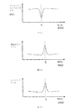
図2bに示すように、CPT共振は、光源によって、たとえば、原子システムにおいてA1からEへの、また、A2からEへのエネルギー遷移に相当する周波数ω1およびω2をそれぞれ有する2つのコヒーレント光電磁場によって誘導される可能性がある。2つのコヒーレント光学場を分離する2つの電磁場ω1およびω2の周波数間の周波数差は、2つの低エネルギー準位A1とA2とのエネルギー差をプランク定数hで割った値に等しい。この光学場が、原子共振に印加される。原子共振器は、2つの準位間で分裂した小さなエネルギーを有する少なくとも1つの低エネルギー状態、および、2つの超微細分裂した低エネルギー状態A1およびA2から、電子がそこに励起されうる少なくとも1つの高エネルギー状態を有する。印加される電磁場の第1の周波数成分ω1は、低エネルギー状態の一方の状態A1から高エネルギー状態Eへ電子を励起し、一方、他の周波数成分は、他の低エネルギー状態A2から同じ高エネルギー状態Eへ電子を励起する。そのため、原子共振器は、印加された電磁場の2つの成分からエネルギーを同時に吸収する。2つの周波数成分間の周波数差が、原子共振器の2つのエネルギー状態間の周波数差に等しいとき、原子共振器は、2つの低エネルギー状態の線形重ね合わせ状態にありうるため、この量子状態では、原子共振器は、もはや印加される電磁場と相互作用しない。この量子状態および結果として得られる挙動は、CPTと呼ばれる。この状態では、原子共振器は、吸収最小か、透過最大か、またはルミネセンスの最小を示す(図3a、3b、および/または3cを相応して参照されたい)。したがって、たとえば、2つの周波数成分間の周波数差が、原子共振器の2つの低エネルギー状態間の周波数差に厳密に等しいとき、光検出器が、上記量の一方の強度を測定するのに使用されてもよい。光検出器は、2つの周波数ω1ω2と超微細エネルギー分裂における周波数差との誤差に相当する信号量を測定し、この誤差信号は、サーボループに対するフィードバックであり、このフィードバックが使用されて、光源によって生成される2つの周波数成分の周波数差が調整され、それにより、2つの周波数ω1ω2と超微細エネルギー分裂における周波数差との誤差が、たとえば、図3a、3b、および/または3cに示すように、最大/最小に維持される。したがって、2つの周波数成分の周波数差は、原子共振器の低エネルギー状態で分裂したエネルギーの周波数差に相当する精密な値に保持される可能性がある。周波数標準の精度および安定性は、原子共振器の低い状態のエネルギーの分裂物間の差の精度および安定性に相当する可能性がある。 As shown in FIG. 2b, the CPT resonance is caused by the light source, for example by two coherent photoelectric fields having frequencies ω1 and ω2 respectively corresponding to energy transitions from A1 to E and from A2 to E in the atomic system. There is a possibility of being induced. The frequency difference between the frequencies of the two electromagnetic fields ω1 and ω2 separating the two coherent optical fields is equal to the energy difference between the two low energy levels A1 and A2 divided by the Planck constant h. This optical field is applied to the atomic resonance. An atomic resonator has at least one low energy state with a small energy split between two levels, and at least one of two hyperfine split low energy states A1 and A2 into which electrons can be excited. Has a high energy state. The first frequency component ω1 of the applied electromagnetic field excites electrons from one state A1 in the low energy state to the high energy state E, while the other frequency component is the same high energy from the other low energy state A2. Excites electrons to state E. As such, the atomic resonator absorbs energy simultaneously from the two components of the applied electromagnetic field. In this quantum state, when the frequency difference between two frequency components is equal to the frequency difference between the two energy states of the atomic resonator, the atomic resonator can be in a linear superposition of the two low energy states. The atomic resonator no longer interacts with the applied electromagnetic field. This quantum state and the resulting behavior is called CPT. In this state, the atomic resonator exhibits an absorption minimum, a transmission maximum, or a luminescence minimum (see correspondingly FIGS. 3a, 3b and / or 3c). Thus, for example, when the frequency difference between two frequency components is exactly equal to the frequency difference between the two low energy states of the atomic resonator, the photodetector is used to measure the intensity of one of the above quantities. May be. The photodetector measures the amount of signal corresponding to the error between the two frequencies ω1ω2 and the frequency difference in the hyperfine energy split, and this error signal is feedback to the servo loop, and this feedback is used by the light source. The frequency difference between the two frequency components generated is adjusted so that the error between the two frequencies ω1ω2 and the frequency difference in the hyperfine energy splitting is, for example, as shown in FIGS. 3a, 3b, and / or 3c, Maintained at max / min. Therefore, the frequency difference between the two frequency components may be held at a precise value corresponding to the frequency difference between the energy split in the low energy state of the atomic resonator. The accuracy and stability of the frequency standard may correspond to the accuracy and stability of the difference between the low energy splits of the atomic resonator.
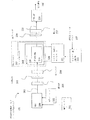
図1は、一部の実証的な実施形態によるSSACを概略的に示す。一部の非制限的な実施形態では、図1のSSAC100は、図9から14の1つまたは複数のSSACの機能を実施してもよい。
FIG. 1 schematically illustrates an SSAC according to some demonstrative embodiments. In some non-limiting embodiments, the
周波数基準を取得する方法は、図8bに示すように、量子状態416の共振に相当する周波数を有するマイクロ波信号413を制御発振器411によって生成することによって実施され、マイクロ波信号の周波数は、固体媒体の色中心の超微細分裂の共振周波数416と比較され418、比較器418の出力信号410が使用されて、色中心共振周波数416の周波数に対してマイクロ波周波数が調整され、マイクロ波周波数が必要とされる周波数に再スケーリングされ414、再スケーリングされた周波数が出力され415、それにより、出力周波数が、色中心共振周波数の周波数を基準にする。
The method for obtaining the frequency reference is implemented by generating a
SSACは、たとえば、以下で詳細に述べるように、制御発振器102と、周波数逓倍器104、固体原子共振器モジュール103、および/またはフィードバック回路101を含んでもよい。
The SSAC may include, for example, a controlled
制御発振器102は、入力として提供される制御信号に応じて、その出力周波数を変更することができる周波数振動発生器である。制御発振器102の周波数出力は、逓倍され、結合され、固体共振器の周波数共振またはエネルギー共振にロックされてもよい。したがって、非常に精密でかつ安定した周波数出力が取得される可能性がある。
The controlled
周波数逓倍器104は、低周波数を有する入力信号を得、高い周波数を有する出力信号を生成することが可能な電子デバイスまたは回路である。出力周波数の値は、入力周波数に、周波数逓倍器104にセットされた数値係数を掛けた値に等しい。図1の周波数逓倍器104は、入力として、制御発振器102から比較的低い周波数を得、出力として、共振器共振周波数に相当する周波数を有する信号を生成する。この周波数は、たとえば、光学および/またはマイクロ波信号送信機を介して、共振器モジュールに供給されてもよい、かつ/または、結合されてもよい。共振器モジュールは、周波数基準として使用される原子共振を使用する。共振器モジュールは、入力として、周波数逓倍器104の出力を受信し、共振器原子共振の内部共振周波数と逓倍器出力周波数107との差に比例する出力誤差信号を生成する。
The
フィードバック回路101は、入力として、固体共振器モジュール103の出力誤差信号106を受信し、制御発振器102に対する誤差補正信号105を生成する。制御発振器102は、たとえば、周波数逓倍器104の出力周波数107と固体共振器219の共振周波数との誤差を減少させるために、この誤差信号を使用して、その出力周波数108、109を補正する。相応して、出力周波数108は、固体原子共振器219の原子共振周波数にロックされてもよい。
The
フィードバック回路101: Feedback circuit 101:
フィードバック回路101は、入力として共振器出力誤差信号を受信し、その誤差信号を、制御発振器102モジュールに提供される補正信号に変換してもよい。原子共振器モジュール103の出力信号は、たとえば、まさに入力周波数と原子共振器219の内部共振周波数が同じである周波数値において、出力信号レベルの極値を有してもよい。原子共振器モジュール出力誤差信号106は、印加されるマイクロ波信号107の周波数と原子共振器219の内部共振周波数との差に比例する。フィードバック回路101の入力に提供される原子共振器モジュール103の出力における誤差信号は、低い信号対雑音比を有する可能性がある。したがって、雑音から誤差信号を抽出するために、フィルタリングおよび/または信号処理スキームが使用されてもよい。たとえば、同期検出スキームが、フィードバック回路101で使用されて、雑音内の非常に小さな信号を検出し、補正誤差信号を推定しうる。SSACが閉ループで動作してもよいため、コントロールシステムは、最大安定性、最小出力周波数雑音、および/または、アラン偏差を達成するために、たとえば、フィードバック回路101の一部として、かつ/または、SSACの任意の他の要素の一部として実施されてもよい。1つの非制限的な実施例では、PIDコントロールスキームが実施されうる。1つの非制限的な実施例では、同期フィルタ、非制限的な実施例の場合、Analog Device Inc.AD630、AD633平衡型変調器/復調器が実施されてもよい。PIDスキームは、演算増幅器(たとえば、Analog Devices Inc.部品番号ADTL082)および受動電子コンポーネントを用いて実施されうる。
The
制御発振器102: Controlled oscillator 102:
制御発振器102は、周波数発振器を含んでもよい。制御発振器102は、フィードバック回路101から入力信号を受信し、その信号を、入力信号の信号レベルに相当する周波数出力信号に変換してもよい。制御発振器102は、たとえば、高いQファクタの電圧制御発振器102、1つの非制限的な実施例では、石英結晶に基づく低周波数発振器を含んでもよい電圧制御水晶発振器(Voltage Controlled Crystal Oscillator)(VCXO)によって実施されてもよい。水晶発振は、非常に高いQファクタおよび良好な短期安定性を有する可能性がある。しかし、水晶発振は、時間経過に伴う周波数ドリフトで表現される長期安定性が非常に低い可能性がある。これらの種類の発振器は、入力電圧レベルに応じて出力周波数の変化を可能にする入力制御電圧を有する。VCXOの出力周波数は、フィードバック回路101によって生成される出力信号に応じて補正されてもよい。1つの非制限的な実施例では、VCXOは、たとえば、その全体の開示が参照により本明細書に組込まれる、A.Brannon, J.Breitbarth,およびZ.Popovic著「A Low−Power, Low Phase Noise Local Oscillator for Chip−Scale Atomic Clocks」IEEE Microwave Theory and Techniques Symposium、印刷中、2005年によって述べられるように、Vectron International V−800 VCXOまたは等価物を含んでもよい。
The controlled
周波数逓倍器104: Frequency multiplier 104:
周波数逓倍器104は、VCXOから周波数入力を受信し、周波数入力を逓倍して、入力周波数に、必要とされる係数を掛けた値に等しい周波数をもたらす可能性がある。出力周波数は、たとえば、本明細書で述べる電磁マイクロ波方法の場合、共振器周波数共振に実質的に等しくてもよく、また、たとえば、本明細書で述べるCPT方法の場合、この周波数の実質的に半分であってよい。1つの非制限的な実施例では、周波数逓倍器104は、PLL(位相ロックループ)、FLL(周波数ロックループ)、周波数混合、および/または任意の他の技法を使用してもよい。周波数逓倍のこれらの方法は、位相雑音を低く維持しながら、周波数の変更を可能にする。1つの非制限的な実施例では、周波数逓倍器104は、たとえば、高度な周波数処理が必要とされる場合、DDS(ダイレクトデジタルシンセサイザ)によって実施されうる。周波数逓倍器104は、1つの非制限的な実施例では、AD809、ADF4212、ADF4213、ADF4218L、ADF4007、または等価物などのAnalog Devices Inc.RF PLL周波数シンセサイザを使用して実施されてもよい。
The
原子共振器モジュール103: Atomic resonator module 103:
原子共振器モジュール103は、入力として、共振器の内部周波数共振に実質的に等しいことが意図される、周波数逓倍器からの入力107としての電磁信号のマイクロ波周波数を受信してもよい(CPTの場合、本明細書で述べるように、この周波数の半分を有する信号が必要とされる)。原子共振器は、たとえば、以下で述べるように、入力周波数107と原子共振器の内部共振周波数との差に実質的に等しい出力誤差信号225を生成してもよい。
The
一部の実施形態では、固体原子共振器モジュール103は、2共振型共振器199として実施されてもよく、2共振型共振器199は、たとえば、以下で述べるように、以下の要素および/またはモジュールの1つまたは複数を含む。以下の要素および/またはモジュールとは、
・励起光源200
・光源電力コントローラ201
・光源波長コントローラ202
・光処理要素は、光偏光コントローラ204、光減衰器205、および/または光波長フィルタ206を含む
・マイクロ波増幅器222
・マイクロ波偏光器221
・マイクロ波電磁放射を量子レゾナント上に送信するマイクロ波送信アンテナ220
・光キャビティ209
・たとえば、本明細書で述べるように、超微細エネルギー分裂を有する可能性があるエネルギー準位システムを有する固体材料220を含む原子共振器要素
・光偏光器207
・光フィルタ224
・光検出器226
・磁場シールド207
である。
In some embodiments, the solid
Light
Light
The light processing element includes a
・
A
・
An atomic resonator element comprising a
-
・
・
It is.
一部の実施形態では、固体原子共振器モジュール103は、CPT共振器299として実施されてもよく、CPT共振器299は、たとえば、以下で述べるように、以下の要素および/またはモジュールの1つまたは複数を含む。以下の要素および/またはモジュールとは、
・励起光源300
・光源電力コントローラ301
・光源波長コントローラ302
・光処理要素は、光偏光コントローラ306、光減衰器307、および/または光波長フィルタ308を含む
・光源を直接変調しうるマイクロ波変調器308
・光キャビティ311
・たとえば、本明細書で述べるように、超微細エネルギー分裂を有する可能性があるエネルギー準位システムを有する固体材料を含む原子共振器312要素
・光偏光器316
・光フィルタ314
・光検出器315
・磁場シールド310
である。
In some embodiments, the solid
Light
Light
The light processing element includes a
・
For example, as described herein, an
-
・
・
It is.
固体共振器219 312
一部の実施形態では、固体共振器は、たとえば、本明細書で述べるように、光キャビティ内に色中心を含む固体材料を含んでもよい。色中心は、空孔、たとえば、材料マトリクス内で1つの原子が欠損しているサイト、または、固体材料マトリクスと異なる1つまたは複数の原子エレメントに関連する空孔であってよい。固体材料マトリクスは、単結晶、多結晶、ナノ結晶、アモルファス、または任意の他の形態でありうる。色中心は、電気的に中性であるかまたは帯電しうる。原子共振器は、単一色中心または多数の色中心のアンサンブルを含んでもよい。色中心は、固体材料マトリクス内でランダムに分散するかまたは順序付けられうる。 In some embodiments, the solid state resonator may include a solid material that includes a color center within the optical cavity, for example, as described herein. The color center may be a void, for example a site where one atom is missing in the material matrix, or a void associated with one or more atomic elements different from the solid material matrix. The solid material matrix can be single crystal, polycrystalline, nanocrystal, amorphous, or any other form. The color center can be electrically neutral or charged. An atomic resonator may include a single color center or multiple color center ensembles. The color centers can be randomly distributed or ordered within the solid material matrix.
固体材料は、以下で述べるように、かつ/または、図6に示すように光キャビティ内に設置されてもよい。色中心は、基底エネルギー状態において超微細エネルギー分裂を有してもよく、1つまたは複数のより高いエネルギー準位を有してもよい。電子は、基底状態から、これらのより高いエネルギー準位の1つのエネルギー準位に励起されうる。超微細共振分裂は、たとえば、本明細書で述べるように、光学的に検出されたマイクロ波放射励起によって、または、光学的に検出されたCPTによって読み出されうる。基底状態の電子は、コヒーレントなおよび/または非コヒーレントな光源によって、または、任意の他の電磁放射によって励起されうる。励起放射の光子エネルギーまたは波長は、IR範囲内か、可視範囲内か、または、任意の他の適した光子エネルギー内にありうる。 The solid material may be placed in the optical cavity as described below and / or as shown in FIG. The color center may have a hyperfine energy split in the ground energy state and may have one or more higher energy levels. The electrons can be excited from the ground state to one of these higher energy levels. The hyperfine resonant splitting can be read out, for example, by optically detected microwave radiative excitation or by optically detected CPT, as described herein. Ground state electrons can be excited by a coherent and / or incoherent light source, or by any other electromagnetic radiation. The photon energy or wavelength of the excitation radiation can be in the IR range, in the visible range, or in any other suitable photon energy.
図4は、1つの実証的な実施形態による2共振ベースの固体原子共振器モジュール199を概略的に示す。一部の非制限的な実施形態では、図4の固体原子共振器は、図1のSSACの機能を実施する可能性がある。
FIG. 4 schematically illustrates a two-resonance based solid
図4の固体原子共振器モジュール199は、2共振技法によって共振線を測定するための任意の適した方法を実施してもよい。1つの非制限的な実施例では、図4の固体原子共振器モジュール199は、たとえば、その全体の開示が参照により本明細書に組込まれる、T.P.Mayer Alegre,C.Santori,G.Medeiros−Ribeiro,およびR.G.Beausoleil著「Polarization−selective excitation of nitrogen vacancy centers in diamond」Physical Review B 76,165205(2007)によって述べられるように、2共振技法によって色中心における超微細エネルギー分裂の共振線を収集し、自由走行発振器102および周波数逓倍器104のマイクロ波周波数107を、原子共振器103 219内の原子共振に結合させる方法を実施してもよい。
The solid
波長コントローラ202 300および電力コントローラ201 301を有する光源200 302は、たとえば、本明細書で述べるように、線形偏光器204 306、光減衰器206 307、および光フィルタ206 308を通して、固体共振器219 312を照射するように実施されてもよい。照射光203 305の波長は、たとえば、以下で述べるように、ダイアモンド内の窒素空孔(Nitrogen Vacancy)(NV)中心の基底エネルギー準位3A内の電子を、励起エネルギー準位3Eまで励起しうる、637nmまたは532nmのゼロフォノン線(Zero Phonon Line)(ZPL)でありうるが、それに限定されない。
A
非制限的な実施例では、たとえば、以下で述べるように、ダイアモンド内のNV中心を、光源200、すなわち、偏光した637nm光子かまたは532nm光子によって照射することによって、基底エネルギー準位3Aから励起エネルギー準位3Eのサブ準位のうちの1つの準位までポンピングすることは、電子の基底状態への緩和によってフォトルミネセンスをもたらす。3A基底エネルギーのms=0スピン状態へ緩和する確率はずっと高く、結果として、電子は、定常状態における3A基底エネルギー状態のms=0スピン状態で蓄積する。結果として、NV中心のフォトルミネセンスは、定常状態で一定である。超微細分裂の周波数に等しい周波数を用いたマイクロ波励起は、基底状態のms=0スピン状態から基底状態のms=±1スピン状態への電子の移動をもたらし、電子の移動は、励起周波数が、図3aおよび3bに述べるように、基底状態エネルギー分裂に厳密に等しいため、フォトルミネセンスと光透過の両方の極値に達する可能性がある。この極値が使用されて、光検出器226によってマイクロ波共振が検出され、共振周波数とマイクロ波との間の誤差に関連する出力信号106が提供される。
In a non-limiting example, for example, as described below, the NV center in the diamond is excited from the ground energy level 3 A by irradiating with a
図5は、別の実証的な実施形態によるCPTベースの固体原子共振器モジュール299を概略的に示す。一部の非制限的な実施形態では、図5の固体原子共振器は、図1のSSACの機能を実施する可能性がある。
FIG. 5 schematically illustrates a CPT-based solid
図5の固体原子共振器モジュール299は、CPT技法によって共振線を測定するための任意の適した方法を実施してもよい。1つの非制限的な実施例では、図5の固体原子共振器モジュール299は、限定はしないが、その全体の開示が参照により本明細書に組込まれる、Charles Santori等著「Coherent Population Trapping of Single Spins in Diamond under Optical Excitation」Phys.Rev.Lett.97,247401(2006)および/またはCharles Santori等著「Coherent Population Trapping in diamond N−V centers at zero magnetic field」Vol.14 NO.17 Opt.Exp.(2006)によって述べられるように、CPT技法によって共振線を測定する方法を実施してもよい。
The solid
2つのコヒーレント波長を有する光源302は、たとえば、本明細書で述べるように、線形偏光器306、光減衰器307、および光フィルタ308を通して固体共振器312を照射してもよい。波長および電力は、2つのコヒーレント波長間の周波数差が、2.88Ghzの基底状態分裂に等しくなるよう同調されるように制御されてもよい。光源波長におけるこの周波数差は、SSACにおいて周波数基準として使用されてもよい外部マイクロ波信号によって生成され、制御される。照射光の波長は、637nmまたは532nm、あるいは、たとえば、以下で述べるように、基底エネルギー準位3Aから励起エネルギー準位3Eのサブ準位のうちの1つの準位までNV中心を励起しうる任意の他の波長のZPLでありうるが、それに限定されない。ある非制限的な実施例では、ダイアモンド内のNV中心を照射することは、ms=0およびms=±1の基底サブ準位エネルギー状態から励起状態3Eまでの電子の励起を同時にもたらす可能性がある。この同時励起は、CPT量子状態をもたらすことになり、結果として、フォトルミネセンスの降下または透過周波数の関数としてのNV中心の透過のピークが存在する。この極値は、周波数逓倍器104からのマイクロ波信号の周波数が、基底状態エネルギー分裂の周波数の半分に厳密に等しくなると発生する。そのため、制御用マイクロ波周波数は、超微細共振にロックされてもよい。
A
光キャビティ209 311
一部の非制限的な実施例では、光キャビティ209 311は、たとえば、その全体の開示が参照により本明細書に組込まれる、J.K.Vahala著「Optical microcavities」Nature(London)424,839(2003)、S.HarocheおよびD.Kleppner著「Cavity quantum electrodynamics」Physics Today,January 1989,pp.24、Y.YamamotoおよびR.Slusher著「Optical processes in microcavities」Physics Today,June 1993,pp.66、C.J.Hood,T.W.Lynn,A.C.Doherty,A.S.Parkins,およびH.J.Kimble著「The atom−cavity;and/or microscope:single atoms bound in orbit by single photons」Science,vol.287,No.25,pp.1447−1453(2000)によって述べられる光キャビティ209 311を含んでもよい。
In some non-limiting examples, the
光キャビティ209 311は、「狭波長(narrow wavelength)」複数反射キャビティを含んでもよい。キャビティ内部には、境界条件に適合する波長および許容される光モードを有する光子だけが保持される。高強度光モードがキャビティ内部で生成される。これらのモードは、固体共振器219 312の色中心と連続して相互作用して、高い量子効率ならびに狭い吸収および放出線をもたらす。1つの非制限的な実施例では、光キャビティ209 311は、たとえば、上述したダイアモンド材料の一部として実施されてもよい。別の非制限的な実施例では、光キャビティ209 311は、別々に実施されてもよく、色中心は、キャビティ内に組込まれてもよい。
The
NV中心は、NV中心を含むマイクロメートルダイアモンド粒子またはナノダイアモンド粒子を含んでもよく、または、ダイアモンドの固体スラブの一部として実施されてもよい。光キャビティは、たとえば、図6に示すように、ファブリペロー、ブラッグミラーまたはブラッグ反射体、フォトニック結晶共振器、外部キャビティ、ファイバブラッグ格子、膜キャビティ、垂直キャビティ、マイクロピラー垂直キャビティ、マイクロディスク、ウィスパリングギャラリー、または任意の他の光キャビティ実施態様を使用して実施されてもよい。 The NV center may comprise micrometer diamond particles or nanodiamond particles containing the NV center, or may be implemented as part of a diamond solid slab. The optical cavity is, for example, as shown in FIG. 6, Fabry-Perot, Bragg mirror or Bragg reflector, photonic crystal resonator, external cavity, fiber Bragg grating, membrane cavity, vertical cavity, micropillar vertical cavity, microdisk, It may be implemented using a whispering gallery, or any other optical cavity implementation.
光キャビティ209 311は、1波長狭帯域、または、1つの帯域が励起波長に同調され、他の帯域が放出またはルミネセンス波長に同調されうる2帯域狭波長でありうるが、それに限定されない。光キャビティ209 311は、放出/ルミネセンス利得を改善する可能性があり、入射光ビームと色中心との相互作用を改善する。光キャビティ209 311は、吸収帯域および放出帯域を狭め、応力および/または他のパラメータによるゼロフォノン線の偏倚および幅広化をなくす可能性がある。
The
ダイアモンド内のNV色中心の実施例 Example of NV color center in diamond
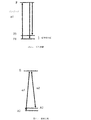
ダイアモンド内のNV色中心の特定の説明は、たとえば、その全体の開示が参照により本明細書に組込まれる、Torsten Gaebel等著「Room−temperature coherent coupling of single spins in diamond」Nature Physics 2,408−413(2006)、R.Hanson,O.Gywat,およびD.D.Awschalom著「Room−temperature manipulation and decoherence of a single spin indiamond」Phys.Rev.B 74,161203(R)(2006)、R.Hanson,F.M.Mendoza,R.J.Epstein,およびD.D.Awschalom著「Polarization and Readout of Coupled Single Spins in Diamond」Phys.Rev.Lett.97,087601(2006)、N.B.Manson,J.P.Harrison,およびM.J.Sellars著「Nitrogen−vacancy center in diamond:Model of the electronic structure and associated dynamics」Phys.Rev.B 74,103303(2006)、Ph.Tamarat等著「The excited state structure of the nitrogen−vacancy center in diamond」arXiv:cond−mat/0610357v1 13 oct 2006、T.P.Mayer Alegre,A.C.Torrezan,G.Medeiros−Ribeiro著「Microstrip resonatorfor microwaves with controlled polarization」Appl.Phys.Lett.91,204103(2007)、T.P.Mayer Alegre,C.Santori,G.Medeiros−Ribeiro,およびR.G.Beausoleil著「Polarization−selective excitation vacancy centers in diamond」Phys.Rev.B 76,165205(2007)、A.P.Nizovtsev,S.Ya.Kilin,F.Jelezko,I.Popa,A.Gruber,J.Wrachtrup著「NV centers in diamond:spin−selective photokinetics, optical ground−state spin alignment and hole burning」Physica B 340−342(2003)、ならびに/または、J.R.Rabeau等著「Implantation of labeled single nitrogen vacancy centers in diamond using 15N」Applied Physical Letters 88,023113(2006)において見出されうる。 A specific description of NV color centers within diamonds is described, for example, by “Storm-temperature coherent coupling of single spins in diamonds” Nature Physics 40, by Torsten Gaebel et al., The entire disclosure of which is incorporated herein by reference. 413 (2006), R.A. Hanson, O .; Gywat, and D.W. D. Awschalom, “Room-temperature manipulation and decoherence of a single spin indiamond” Phys. Rev. B 74, 161203 (R) (2006), R.B. Hanson, F.M. M.M. Mendoza, R.M. J. et al. Epstein, and D.C. D. “Polarization and Readout of Coupled Singles in Diamond” by Awscharom, Phys. Rev. Lett. 97, 087601 (2006), N.R. B. Manson, J. et al. P. Harrison, and M.M. J. et al. Cellars, “Nitrogen-vacancy center in diamond: Model of the electronic structure and associated dynamics” Phys. Rev. B 74, 103303 (2006), Ph. Tamarat et al., “The exact state structure of the nitrogen-vacuum center in diamond” arXiv: cond-mat / 0610357v1 13 oct 2006, T. et al. P. Mayer Alegre, A.M. C. Torrezan, G.M. Mediros-Riveiro, “Microstrip resonator for microwaves with controlled polarization” Appl. Phys. Lett. 91, 204103 (2007), T.W. P. Mayer Alegre, C.I. Santori, G.M. Medeiros-Riveiro, and R.A. G. "Polarization-selective excision vacancy centers in diamond" by Beausoleil, Phys. Rev. B 76, 165205 (2007), A.B. P. Nizovtsev, S.M. Ya. Kilin, F.A. Jelezko, I. et al. Popa, A .; Gruber, J. et al. “NV centers in diamond: spin-selective photokinetics, optical ground-state spin alignment and hole burning” and Physica B 340-342 (2003) by Wrachurup. R. Rabeau et al., “Implementation of labeled single nitrogen vacancy centers in diamond using 15 N”, Applied Physical Letters 88, 023113 (2006).
ダイアモンド内のNV中心は、空孔、たとえば、炭素原子の欠如を含んでもよく、図7bに示すように、空孔の周りの6つの原子サイトのうちの1つのサイト内に1つの窒素置換原子が存在する。NV中心は、中心内の置換原子として窒素かまたは窒素同位体でありうる。負に帯電した状態(NV−)では、この色中心は、非常に高い光安定性および室温安定性を有する。NV中心は、スピントリプレット(S=1)基底状態3Aおよびスピントリプレット(S=1)励起状態3Eを有する。基底状態は、スピンシングレットSz(ms=0)とスピンダブレットSx Sy(ms=±1)とのサブ準位間で2.88Ghzの非常に安定した超微細ゼロ場分裂および準安定1Aエネルギー状態を有する。3Aから3EへのZPL遷移は、スピン保存的であり、図7aに示すように、非常に強い光遷移および高い量子効率を有する。電子は、3Aエネルギー状態と3Eネルギー状態との間の線形偏光光励起によって基底エネルギー準位のms=0状態で蓄積する可能性があり、フォトルミネセント光子を放出することによって基底ms=0サブ準位に緩和した。励起状態3Eからms=0スピン状態3A基底エネルギー状態への光放出遷移は、さらなる準安定エネルギー準位1A(ms=0スピン状態3A基底エネルギー状態への強い非放射エネルギー遷移を有する)による、3A基底エネルギー状態のms=±1への遷移による放出に比べてずっと大きい。色中心のこれらの2つの特性は、たとえば、超微細エネルギー分裂周波数に実質的に正確に等しい周波数を有するマイクロ波励起を適用することによって、たとえば、基底状態の超微細構造を光学的に分解することを可能にする可能性がある。このマイクロ波放射は、ポンピングされた電子をms=0準位からms=1準位まで励起し、それにより、フォトルミネンセンス強度の減少をもたらす可能性がある。 The NV center in the diamond may contain vacancies, eg, lack of carbon atoms, and one nitrogen substitution atom in one of the six atomic sites around the vacancies, as shown in FIG. 7b. Exists. The NV center can be nitrogen or a nitrogen isotope as a substitution atom within the center. In the negatively charged state (NV−), this color center has very high light and room temperature stability. The NV center has a spin triplet (S = 1) ground state 3 A and a spin triplet (S = 1) excited state 3 E. The ground state is a very stable hyperfine zero-field splitting and metastable 1 A energy state of 2.88 Ghz between the sublevels of the spin singlet Sz (ms = 0) and the spin doublet Sx Sy (ms = ± 1). Have The 3 A to 3 E ZPL transition is spin conservative and has a very strong optical transition and high quantum efficiency, as shown in FIG. 7a. Electrons can accumulate in the ms = 0 state of the ground energy level by linearly polarized light excitation between the 3 A energy state and the 3 E energy state, and the basis ms = 0 by emitting photoluminescent photons. Relaxed to sub-level. The photoemission transition from excited state 3 E to ms = 0 spin state 3 A ground energy state has a strong non-radiative energy transition to a further metastable energy level 1 A (ms = 0 spin state 3 A ground energy state ) Due to the transition from 3 A ground energy state to ms = ± 1. These two properties of the color center, for example, optically resolve the ground state hyperfine structure, for example by applying microwave excitation having a frequency substantially exactly equal to the hyperfine energy splitting frequency. There is a possibility to make it possible. This microwave radiation can excite the pumped electrons from the ms = 0 level to the ms = 1 level, thereby resulting in a decrease in photoluminescence intensity.
色中心における3A基底状態と3E励起状態との間のZPL光遷移は、非常に高い量子効率を有し、たとえ単一光中心であってもルミネセンス検出を可能にする。3A基底エネルギー準位は、2つの基底エネルギー準位間の超微細エネルギー分裂のために分裂する。低い準位は、2.88Ghzのスピン分裂を有する。エネルギー共振は、たとえば、先に説明したように、光−マイクロ波共振によって、または、CPTによって読取られうる。ダイアモンドは、低いフォノン密度を有し、したがって、色中心とダイアモンド内のフォノンとの間の相互作用は低い。基底状態は、電子スピン状態の長いデコヒーレンス時間を有する。他の材料内の色中心の共振線と比べて、非常に急峻な共振線が、室温でも検出されうる。NV色中心は、637nmのZPLから450nm未満までの広い吸収帯域を有し、NV中心の放出帯域は、637nmのZPLから、637nmと750nmとの間の振動放出帯域までであり、シリコン光検出器によって容易に検出されうる。この吸収および放出共振線ならびに吸収および放出線帯域は、色中心のフォトルミネセンスを励起し測定するのに使用されうる。ダイアモンドは、可視スペクトルの広い透明窓を有する、非常に安定した材料でかつ広バンドギャップ半導体材料である。ダイアモンドは、非常に良好な熱伝導体であり、また、たとえば、ドーピングすると、非常に良好な絶縁体または非常に良好な導体になりうる。 The ZPL light transition between the 3 A ground state and the 3 E excited state at the color center has a very high quantum efficiency, allowing luminescence detection even with a single light center. The 3 A ground energy level splits due to hyperfine energy splitting between the two ground energy levels. The lower level has a spin splitting of 2.88 Ghz. The energy resonance can be read, for example, by optical-microwave resonance or by CPT as described above. Diamond has a low phonon density, so the interaction between the color center and the phonons in the diamond is low. The ground state has a long decoherence time of the electron spin state. Compared with the color center resonance line in other materials, a very steep resonance line can be detected even at room temperature. The NV color center has a broad absorption band from 637 nm ZPL to less than 450 nm, the NV center emission band is from 637 nm ZPL to the vibrational emission band between 637 nm and 750 nm, and a silicon photodetector. Can be easily detected. The absorption and emission resonance lines and absorption and emission line bands can be used to excite and measure color-centered photoluminescence. Diamond is a very stable and wide bandgap semiconductor material with a transparent window with a wide visible spectrum. Diamond is a very good thermal conductor and, for example, when doped, can be a very good insulator or a very good conductor.
図7aは、NV色中心のエネルギー準位図を概略的に示す。 FIG. 7a schematically shows an energy level diagram of the NV color center.
図7bは、ダイアモンド格子内のNV中心構造を概略的に示す。灰色球は、ダイアモンド格子内の炭素原子を表し、「N」球は窒素原子を表し、「V」球は、ダイアモンド格子内の空孔、原子の欠如を表す。 FIG. 7b schematically shows the NV center structure in the diamond lattice. Gray spheres represent carbon atoms in the diamond lattice, “N” spheres represent nitrogen atoms, and “V” spheres represent vacancies in the diamond lattice, lack of atoms.
ダイアモンド内でのNV色中心形成および作製は、たとえば、その全体の開示が参照により本明細書に組込まれる、米国特許4880613および/またはJ.R.Rabeau等著「Implantation of labeled single nitrogen vacancy centers in diamond using 15N」Applied Physical Letters 88,023113(2006)に記載される。 NV color center formation and creation in diamond is described, for example, in US Pat. No. 4,880,613 and / or J. Pat. R. Rabeau et al., “Implementation of labeled single nitrogen vacance centers in diamond using 15 N”, Applied Physical Letters 88, 0231113 (2006).
NV色中心は、タイプIIaとタイプIbの両方の天然ダイアモンドにおいて種々の濃度で見出されうる。制御された濃度および分散を有するダイアモンド内にNV色中心を作るために、通常、非常に低いレベルから非常に高いレベルの窒素含量を有するタイプIIaまたはタイプIbの天然または合成ダイアモンドが、中性子、電子、またはイオンで照射され、ダイアモンド格子内に空孔を作る。これらの空孔は、600〜1000℃の温度でアニーリングすると、窒素サイトまで拡散して、たとえば、図7bに示すようにNV色中心を作る。 NV color centers can be found in various concentrations in both Type IIa and Type Ib natural diamonds. In order to create NV color centers in diamonds with controlled concentration and dispersion, natural or synthetic diamonds of type IIa or type Ib, usually with very low to very high levels of nitrogen content, are neutrons, electrons Or bombarded with ions to create vacancies in the diamond lattice. When these vacancies are annealed at a temperature of 600-1000 ° C., they diffuse to the nitrogen sites, creating, for example, NV color centers as shown in FIG. 7b.
一部の非制限的な実施例では、本明細書で述べるSSACは、たとえば、SSACのコンポーネントの全てを含む、たとえば、ディスクリートコンポーネントとして集積化されうる。 In some non-limiting examples, the SSAC described herein can be integrated, for example, as a discrete component, including, for example, all of the components of SSAC.
図8aに示すように、1つの非制限的な実施例では、本明細書で述べる原子クロックは、チップスケール原子クロック402として実施されてもよい。たとえば、原子クロックは、半導体チップ400の一部として集積化されてもよい。半導体チップは、たとえば、原子クロックの光検出器405および/または光源403を含む集積回路401として電子回路の全セットを含んでもよい。原子クロックの原子共振器404は、基材400の一部として実施されてもよく、または、基材の一番上に挿入されてもよい。
As shown in FIG. 8 a, in one non-limiting example, the atomic clock described herein may be implemented as a chip scale
本明細書で述べる色中心SSACは、たとえば、ガスベースの原子クロック、たとえば、Rb/Csベースの原子クロックと比較して、以下の利点の少なくとも1つまたは複数を有する可能性がある。
1.無毒か、揮発性か、または、他の有害でない材料が固体共振器に使用される。
2.SSACは、共振器の絶え間ない加熱を必要としなくてもよく、したがって、たとえば、適切な動作に達するために絶えず加熱されなければならない(これは、高い電力消費をもたらす)ガスセルベースの原子クロックと比較すると、低い電力消費を有する可能性がある。
3.SSAC内の共振媒体は、1ミリメートル平方より小さいサイズを有する固体材料を含む可能性がある。こうした共振器の製造コストは、たとえば、非常に複雑な製造プロセスを有するガスセルと比較すると、非常に低い。
4.光励起波長は、たとえば、630nmから450nm未満までの広い範囲を有する。これは、低コスト固体VIS光源による光源の実施態様を可能にする可能性がある。
5.蛍光波長は、たとえば、630nmから700nm以上までの広い範囲を有し、低コストシリコン光検出器を使用することを可能にする可能性がある。
6.サイズが小さい−SSAC共振器は、色中心によって埋め込まれた固体結晶を含んでもよく、色中心のサイズは、たとえば、1ミリメートル平方において、最高10個が見出されうるように、数ナノメートルであってよい。
7.重力耐久性−本質的に、ガスは、固体に比べて重力に対する感度がずっと高い。ガスに重力を印加することは、ガスの圧縮をもたらし、均質なガス密度を生成する。したがって、光が異なる原子密度を経験するガスを通過すると、このエピソード中に、強度不安定性がもたらされる。この不安定性は、出力周波数信号の不安定性をもたらす。
8.経年変化−SSAC、たとえば、ダイアモンドベースの固体原子クロックの経年変化は、ガスベースの原子クロックと比較して著しく小さい可能性がある。原子ガスセルは、セル壁、接着剤からの残留ガス分子の放出および拡散により経年変化を受ける。したがって、ガス混合物の純度が、動作中に低下し、結果として、原子クロックの性能が低下する。一方、SSACは、たとえば、上述したように、最も安定性のある材料であるダイアモンドに基づいてもよい。
9.リビジウム標準に伴う磨滅現象がない。
10.たとえば、ガスベースの原子時計の長い暖気運転時間と比較して、暖気運転時間が非常に短い。
11.低い電力消費−ガス共振器では、ガスセルは、適切な動作を達成するために、連続して加熱されなければならず、高い電力消費をもたらす。これは、本明細書で述べるSSAC共振器では必要とされない可能性がある。
The color center SSAC described herein may have at least one or more of the following advantages compared to, for example, a gas-based atomic clock, eg, an Rb / Cs-based atomic clock.
1. Non-toxic, volatile or other non-hazardous materials are used for the solid resonator.
2. SSACs may not require constant heating of the resonator, and therefore must be constantly heated to achieve proper operation, for example (which results in high power consumption) and a gas cell based atomic clock In comparison, it may have low power consumption.
3. Resonant media in SSAC can include solid materials having a size of less than 1 millimeter square. The cost of manufacturing such a resonator is very low compared to, for example, a gas cell with a very complex manufacturing process.
4). The photoexcitation wavelength has a wide range from, for example, 630 nm to less than 450 nm. This may allow light source implementations with low cost solid state VIS light sources.
5. The fluorescence wavelength has a wide range, for example, from 630 nm to over 700 nm, which may allow the use of low cost silicon photodetectors.
6). Small size—SSAC resonators may include solid crystals embedded by color centers, where the size of the color center is, for example, a few nanometers so that up to 10 can be found in 1 millimeter square It may be.
7). Gravity durability-In essence, gases are much more sensitive to gravity than solids. Applying gravity to the gas results in compression of the gas and produces a homogeneous gas density. Thus, when light passes through a gas that experiences a different atomic density, intensity instability occurs during this episode. This instability results in instability of the output frequency signal.
8). Aging—SSAC, for example, the aging of diamond-based solid atomic clocks can be significantly smaller compared to gas-based atomic clocks. Atomic gas cells are subject to aging due to the release and diffusion of residual gas molecules from the cell walls and adhesives. Thus, the purity of the gas mixture decreases during operation, resulting in a decrease in the performance of the atomic clock. On the other hand, SSAC may be based on diamond, which is the most stable material, for example, as described above.
9. There is no wear-out phenomenon associated with the Ribidium standard.
10. For example, the warm-up time is very short compared to the long warm-up time of a gas-based atomic clock.
11. Low power consumption—In gas resonators, the gas cell must be continuously heated to achieve proper operation, resulting in high power consumption. This may not be required for the SSAC resonator described herein.
付加的に、または、別法として、本明細書で述べる色中心SSACは、以下の利点の少なくとも1つまたは複数を有する可能性がある。色中心がその中に埋め込まれる材料は、広い光透過性を有する。したがって、色中心は、光手段によってアドレス指定されうる。色中心の量子状態は、光学的に調製されうる、かつ/または、読み出されうる。本明細書で述べる色中心SSACは、電気雑音に対する低減された感度を有する可能性がある。 Additionally or alternatively, the color center SSAC described herein may have at least one or more of the following advantages. The material in which the color center is embedded has a wide light transmission. Thus, the color center can be addressed by the light means. The color-centric quantum state can be optically prepared and / or read out. The color center SSAC described herein may have reduced sensitivity to electrical noise.
本明細書で述べる色中心SSACは、たとえば、OCXO(オーブン制御水晶発振器)クロック、たとえば、Vectron TC−140温度補償型石英結晶発振器と比較して、以下の利点の少なくとも1つまたは複数を有する可能性がある。
1.OCXOの安定性と比べて高い温度安定性。
2.長期(その周波数がドリフトすることになる長期−数日、数週間、数ヶ月にわたる)周波数安定性を改善する。
3.低い電力消費。
4.小さなサイズ。
5.低いコスト−OCXOは、共振器の低い製造収率を有する。
6.外部加速を加えられた状態での重力衝撃−石英結晶は、ニュートンの力を受ける。この力は、石英結晶を変化させ、変形することになり、結果として、結晶の物理的寸法から直接導出される出力周波数の誤差が発生することになる。
7.経年変化−長期変形、内部応力の変化および質量拡散は、OCXO共振器の共振周波数の変化をもたらす。
8.短い暖気運転時間。
The color center SSAC described herein may have at least one or more of the following advantages compared to, for example, an OCXO (Oven Controlled Crystal Oscillator) clock, such as a Vector TC-140 temperature compensated quartz crystal oscillator: There is sex.
1. High temperature stability compared to OCXO stability.
2. Improve frequency stability over the long term (long term where the frequency will drift-over days, weeks, months).
3. Low power consumption.
4). Small size.
5. Low cost—OCXO has a low manufacturing yield of resonators.
6). Gravity impact with external acceleration applied-quartz crystals receive Newtonian forces. This force will change and deform the quartz crystal, resulting in an error in the output frequency that is directly derived from the physical dimensions of the crystal.
7). Aging—long-term deformation, changes in internal stress and mass diffusion result in changes in the resonant frequency of the OCXO resonator.
8). Short warm-up operation time.
一部の実施形態は、たとえば、以下で詳細に述べるように、たとえば、固体材料内の原子共振に基づいて、正確な、かつ/または、安定した出力周波数を生成する原子クロック周波数発生器(「固体原子クロック(SSAC)」)を含んでもよい。SSACは、たとえば、以下で詳細に述べるように、任意の適したデバイス、モジュール、要素、および/または、システムの一部として実施されてもよい。 Some embodiments, for example, as described in detail below, are atomic clock frequency generators ("" that generate accurate and / or stable output frequencies based on, for example, atomic resonances in a solid material. Solid atomic clock (SSAC) "). SSAC may be implemented as part of any suitable device, module, element, and / or system, for example, as described in detail below.
周波数標準SSACを利用する汎用電子モジュールおよび/またはシステムは、図8cに概略的に示される。モジュールおよび/またはシステムは、入力データを受信する入力回路と、出力データを送信する出力回路と、中央処理ユニット(CPU)と、メモリユニットと、RF回路と、アナログおよび/またはデジタル回路と、固体原子クロックを備える。この電子モジュールおよび/またはシステムは、以下で述べる用途のそれぞれを実施するのに、全体として、または、部分的に役立ちうる。 A general purpose electronic module and / or system that utilizes a frequency standard SSAC is shown schematically in FIG. 8c. The module and / or system includes an input circuit that receives input data, an output circuit that transmits output data, a central processing unit (CPU), a memory unit, an RF circuit, an analog and / or digital circuit, and a solid state. Equipped with an atomic clock. The electronic module and / or system may serve in whole or in part to implement each of the applications described below.
図9aは、一部の実証的な実施形態による全地球測位システム(GPS)受信機を概略的に示す。全地球測位システムは、システム位置を収集するために、非常に高いクロック精度を必要とする可能性がある。高精度ローカル発振器または周波数標準またはSSACによって提供されるこの正確な周波数は、GPS衛星のうちの1つの衛星によって格納されるか、または、そこから取出されうる。しかし、基準周波数を保持し、受信機の同期を改善するために必要とされる高精度ローカル発振器または周波数標準は、ジャミングおよび他の干渉を免れない。可搬型の耐ジャミングGPS用途では、小さなサイズ、低電力消費、および低コスト周波数基準が必要とされる。こうした、精度が高く、サイズが小さく、電力消費が低く、コストが低いローカル周波数基準発振器または周波数標準は、たとえば、本明細書で述べるように、SSACによって実現されうる。 FIG. 9a schematically illustrates a global positioning system (GPS) receiver according to some demonstrative embodiments. Global positioning systems can require very high clock accuracy to collect system locations. This precise frequency provided by a precision local oscillator or frequency standard or SSAC can be stored or retrieved from one of the GPS satellites. However, the precision local oscillator or frequency standard required to maintain the reference frequency and improve receiver synchronization is subject to jamming and other interference. In portable jamming resistant GPS applications, small size, low power consumption, and low cost frequency standards are required. Such a local frequency reference oscillator or frequency standard with high accuracy, small size, low power consumption, and low cost can be realized by SSAC, for example, as described herein.
図9bは、一部の実証的な実施形態による携帯電話基地局を概略的に示す。携帯電話基地局は、周波数標準、たとえば限定はしないが、基地局間の携帯電話ハンドセットのホールドオーバを使用してもよい。さらに、最新の基地局バックホールは、インターネットプロトコル(IP)バックホールに基づく可能性があり、高いサービスレベル保証を維持し、ネットワークにわたる精密周波数配信が必要とされる。移動体ネットワーク内での音声、ビデオ、およびデータの伝送は、安定しかつ精密な周波数基準を必要とし、精密な周波数同期が、基地局間の首尾よい呼信号ハンドオフにとって重要である。安定しかつ精密なこうした周波数基準を維持するための考えられる1つの解決策は、たとえば、本明細書で述べるように、SSACを使用することによる。 FIG. 9b schematically illustrates a mobile phone base station according to some demonstrative embodiments. The cell phone base station may use a frequency standard, for example, but not limited to, a cell phone handset holdover between base stations. In addition, modern base station backhaul may be based on Internet Protocol (IP) backhaul, requiring high service level guarantees and precise frequency distribution across the network. The transmission of voice, video, and data within a mobile network requires a stable and precise frequency reference, and precise frequency synchronization is important for successful call signal handoff between base stations. One possible solution to maintain such a frequency reference that is stable and precise is, for example, by using SSAC, as described herein.
図9cは、一部の実証的な実施形態によるセキュア通信システムを概略的に示す。システムは、限定はしないがたとえば、セキュア通信の場合、「時間シーケンスコード収集(time sequence code acquisition)」、または、精密なタイミングに基づくセキュア通信の場合、任意の他の方法を使用しうる。セキュア通信システムは、情報および通信の暗号化のために非常に正確な周波数を使用する可能性がある。安定しかつ精密なこうした周波数基準を維持するための考えられる1つの解決策は、たとえば、本明細書で述べるように、SSACを使用することによる。 FIG. 9c schematically illustrates a secure communication system according to some demonstrative embodiments. The system may use, but is not limited to, for example, “time sequence code acquisition” for secure communications, or any other method for secure communications based on precise timing. A secure communication system may use a very accurate frequency for information and communication encryption. One possible solution to maintain such a frequency reference that is stable and precise is, for example, by using SSAC, as described herein.
図10aは、一部の実証的な実施形態による携帯電話測位システムを概略的に示す。よる携帯電話測位システムは、基地局と携帯電話受信機との間で電磁パスルの到達時間(Time of Arrival)(TOA)を測定することによる、携帯電話受信機と携帯電話基地局との間の距離を確定するために、高精度周波数を使用する可能性がある。安定しかつ精密なこうした周波数基準を維持するための考えられる1つの解決策は、たとえば、本明細書で述べるように、SSACを使用することによる。 FIG. 10a schematically illustrates a mobile phone positioning system according to some demonstrative embodiments. The mobile phone positioning system according to the present invention is based on measuring the time of arrival (TOA) of electromagnetic pulses between the base station and the mobile phone receiver. A high precision frequency may be used to determine the distance. One possible solution to maintain such a frequency reference that is stable and precise is, for example, by using SSAC, as described herein.
図10bは、一部の実証的な実施形態によるインターネットプロトコルTV(IPTV)を概略的に示す。IPTVブロードキャストは、インターネットプロトコル(IP)バックホールに基づき、高いサービスレベル保証を維持し、したがって、ネットワークにわたる精密周波数配信が必要とされる。IPネットワーク内でのビデオおよびデータの伝送は、安定しかつ精密な周波数基準を必要とし、精密な周波数同期が、サーバおよびネットワークスイッチならびにエンドユーザシステムにおけるビデオ信号の首尾よいタイミング再構成にとって重要である。安定しかつ精密なこうした周波数基準を維持するための考えられる1つの解決策は、たとえば、本明細書で述べるように、SSACを使用することによる。 FIG. 10b schematically illustrates an Internet protocol TV (IPTV) according to some demonstrative embodiments. IPTV broadcasts are based on Internet Protocol (IP) backhaul and maintain a high service level guarantee and therefore require precise frequency distribution across the network. Transmission of video and data within an IP network requires a stable and precise frequency reference, and precise frequency synchronization is critical for successful timing reconstruction of video signals in servers and network switches and end-user systems . One possible solution to maintain such a frequency reference that is stable and precise is, for example, by using SSAC, as described herein.
図10cは、一部の実証的な実施形態によるスペクトル拡散ホッピング無線通信システムを概略的に示す。非常に高速な周波数ホッピング無線通信は、異なる周波数間をホッピングすることによって、広帯域の周波数を通じてデータを送出する任意の適した無線通信システムを含んでもよい。非常に高速な周波数ホッピング無線通信では、無線受信機および送信機は、2つの無線システム間で能動的に同期することなく、長期にわたり周波数同期すべきである。こうした無線システムは、軍事用無線、民生用無線、ワイイヤレス無線通信、携帯電話通信、WiMax、WiFi、スペクトル拡散通信、または、任意の他のホッピング無線通信でありうる。安定しかつ精密なこうした周波数基準を維持するための考えられる1つの解決策は、たとえば、本明細書で述べるように、SSACを使用することによる。 FIG. 10c schematically illustrates a spread spectrum hopping wireless communication system according to some demonstrative embodiments. Very fast frequency hopping wireless communications may include any suitable wireless communication system that sends data over a wideband frequency by hopping between different frequencies. In very fast frequency hopping wireless communications, the wireless receiver and transmitter should be frequency synchronized over time without actively synchronizing between the two wireless systems. Such a radio system may be military radio, consumer radio, wireless radio communication, mobile phone communication, WiMax, WiFi, spread spectrum communication, or any other hopping radio communication. One possible solution to maintain such a frequency reference that is stable and precise is, for example, by using SSAC, as described herein.
図11aは、一部の実証的な実施形態による通信局を概略的に示す。通信ネットワークは、ネットワークにわたる精密周波数配信を維持することを必要とする。移動体ネットワーク内での音声、ビデオ、およびデータの伝送は、安定しかつ精密な周波数基準を必要とし、精密な周波数同期および保持が、局間の首尾よい通信にとって重要である。安定しかつ精密なこうした周波数基準を維持するための考えられる1つの解決策は、たとえば、本明細書で述べるように、SSACを使用することによる。 FIG. 11a schematically illustrates a communication station according to some demonstrative embodiments. Communication networks require maintaining precise frequency distribution across the network. The transmission of voice, video, and data within a mobile network requires a stable and precise frequency reference, and precise frequency synchronization and maintenance is important for successful communication between stations. One possible solution to maintain such a frequency reference that is stable and precise is, for example, by using SSAC, as described herein.
図11bは、一部の実証的な実施形態による測位および/またはレンジ測定システムを有する携帯電話ハンドセット受信機を概略的に示す。携帯電話ハンドセット上のレンジファイディングシステム、速度測定システムは、到達時間(TOA)アルゴリズムまたは任意の他のアルゴリズムによって送信機/受信機と対象物との間の距離を確定するために高精度周波数を使用する可能性がある、かつ/または、高精度クロックが、ホールドーバのために使用される可能性がある。安定しかつ精密なこうした周波数基準を維持するための考えられる1つの解決策は、たとえば、本明細書で述べるように、SSACを使用することによる。 FIG. 11b schematically illustrates a mobile phone handset receiver having a positioning and / or range measurement system according to some demonstrative embodiments. Range finding systems on cell phone handsets, speed measurement systems use high precision frequencies to determine the distance between transmitter / receiver and object by time of arrival (TOA) algorithm or any other algorithm. A high-precision clock may be used for the holder. One possible solution to maintain such a frequency reference that is stable and precise is, for example, by using SSAC, as described herein.
図11cは、一部の実証的な実施形態によるホールドオーバシステムを有する携帯電話ハンドセット受信機を概略的に示す。携帯電話ハンドセット上の、携帯電話システムの2つの基地局間のホールドオーバシステムは、到達時間(TOA)アルゴリズムまたは任意の他のアルゴリズムによって送信機/受信機と対象物との間の距離を確定するために高精度周波数を使用する可能性がある、かつ/または、高精度クロックが、ホールドオーバのために使用される可能性がある。安定しかつ精密なこうした周波数基準を維持するための考えられる1つの解決策は、たとえば、本明細書で述べるように、SSACを使用することによる FIG. 11c schematically illustrates a mobile phone handset receiver with a holdover system according to some demonstrative embodiments. A holdover system between two base stations of a mobile phone system on a mobile phone handset determines the distance between the transmitter / receiver and the object by a time of arrival (TOA) algorithm or any other algorithm. May use a high precision frequency and / or a high precision clock may be used for holdover. One possible solution to maintain such a frequency reference that is stable and precise is, for example, by using SSAC, as described herein.
図12aは、一部の実証的な実施形態によるバースト無線通信システムを概略的に示す。バースト無線通信は、無線周波数を通じて音声、ビデオ、およびデータのバーストを送出する任意の適した無線通信システムを含んでもよい。このタイプのシステムでは、無線受信機および送信機は、2つの無線システム間で能動的に同期することなく、長期にわたる精密周波数同期を有するべきである。こうした無線システムは、軍事用無線、民生用無線、ワイイヤレス無線通信、携帯電話通信、または、任意の他のホッピング無線通信でありうる。安定しかつ精密なこうした周波数基準を維持するための考えられる1つの解決策は、たとえば、本明細書で述べるように、SSACを使用することによる。 FIG. 12a schematically illustrates a burst wireless communication system according to some demonstrative embodiments. Burst wireless communication may include any suitable wireless communication system that transmits bursts of voice, video, and data over a radio frequency. In this type of system, the radio receiver and transmitter should have precise frequency synchronization over time without actively synchronizing between the two radio systems. Such a radio system can be military radio, consumer radio, wireless radio communication, cellular telephone communication, or any other hopping radio communication. One possible solution to maintain such a frequency reference that is stable and precise is, for example, by using SSAC, as described herein.
図12bは、一部の実証的な実施形態による敵味方識別装置(IFF)モジュールを概略的に示す。たとえば、飛行中の航空機を特定するために無線通信を使用するIFFシステムは、無線通信のために高精度周波数を使用する可能性がある。安定しかつ精密なこうした周波数基準を維持するための考えられる1つの解決策は、たとえば、本明細書で述べるように、SSACを使用することによる。 FIG. 12b schematically illustrates an enemy ally identification device (IFF) module according to some demonstrative embodiments. For example, an IFF system that uses wireless communication to identify an aircraft in flight may use a high precision frequency for wireless communication. One possible solution to maintain such a frequency reference that is stable and precise is, for example, by using SSAC, as described herein.
図12cは、一部の実証的な実施形態による測定システムを概略的に示す。測定システム、たとえば、ジッタ/ワンダ測定システム、無線周波数測定システム、または他の測定システムは、高精度周波数タイムベースを必要とする。安定しかつ精密なこうした周波数基準を維持するための考えられる1つの解決策は、たとえば、本明細書で述べるように、SSACを使用することによる。 FIG. 12c schematically illustrates a measurement system according to some demonstrative embodiments. Measurement systems such as jitter / wander measurement systems, radio frequency measurement systems, or other measurement systems require a high precision frequency time base. One possible solution to maintain such a frequency reference that is stable and precise is, for example, by using SSAC, as described herein.
図13aは、一部の実証的な実施形態による時間サーバを概略的に示す。時間サーバは、精密な計時能力を有する任意の適した通信ネットワークコンポーネントを含んでもよい。時間サーバは、通信ネットワークに接続されてもよく、時間インジケータをネットワークの他のコンポーネントに送出しうる。時間サーバは、独立型でありうる、または、サーバ、スイッチ、またはハブなどのネットワーク内の別のシステムに埋め込まれうる。安定しかつ精密なこうした周波数基準を維持するための考えられる1つの解決策は、たとえば、本明細書で述べるように、SSACを使用することによる。 FIG. 13a schematically illustrates a time server according to some demonstrative embodiments. The time server may include any suitable communication network component that has precise timing capabilities. The time server may be connected to a communication network and may send a time indicator to other components of the network. The time server can be standalone or embedded in another system in the network, such as a server, switch, or hub. One possible solution to maintain such a frequency reference that is stable and precise is, for example, by using SSAC, as described herein.
図13bは、一部の実証的な実施形態による精密ネットワーク解析器システムを概略的に示す。精密ネットワーク測定システムは、侵入検出、パケットの喪失、および他の要件を含むサービスの品質を測定するために、通信ネットワークの性能を監視する任意の適した通信ネットワークコンポーネントを含んでもよい。システムは、ネットワーク内の発生する任意のイベントを精密にログに記録するために、精密な計時能力を必要とする可能性がある。システムは、通信ネットワークに接続され、独立型でありうる、または、サーバ、スイッチ、またはハブなどのネットワーク内の他のシステムに埋め込まれうる。安定しかつ精密なこうした周波数基準を維持するための考えられる1つの解決策は、たとえば、本明細書で述べるように、SSACを使用することによる。 FIG. 13b schematically illustrates a precision network analyzer system according to some demonstrative embodiments. The precision network measurement system may include any suitable communication network component that monitors the performance of the communication network to measure quality of service, including intrusion detection, packet loss, and other requirements. The system may require precise timing capabilities to accurately log any event that occurs in the network. The system may be connected to a communication network and stand alone or embedded in other systems in the network such as servers, switches, or hubs. One possible solution to maintain such a frequency reference that is stable and precise is, for example, by using SSAC, as described herein.
図13cは、一部の実証的な実施形態による料金請求システムを概略的に示す。ネットワーク通信料金請求システムは、サービスおよび使用のための料金を請求するために、通信ネットワークのトラフィックを監視する任意の適した通信ネットワークコンポーネントを含んでもよい。システムは、ネットワーク任意の使用を精密にログに記録するために、精密な計時能力を必要とする可能性がある。システムは、通信ネットワークに接続され、独立型でありうる、または、サーバ、スイッチ、またはハブなどのネットワーク内の他のシステムに埋め込まれうる。安定しかつ精密なこうした周波数基準を維持するための考えられる1つの解決策は、たとえば、本明細書で述べるように、SSACを使用することによる。 FIG. 13c schematically illustrates a billing system according to some demonstrative embodiments. The network communication billing system may include any suitable communication network component that monitors communication network traffic to charge for service and usage. The system may require precise timekeeping capabilities to accurately log any use of the network. The system may be connected to a communication network and stand alone or embedded in other systems in the network such as servers, switches, or hubs. One possible solution to maintain such a frequency reference that is stable and precise is, for example, by using SSAC, as described herein.
図14aは、一部の実証的な実施形態によるレーダシステムを概略的に示す。レーダシステムは、エコー無線波信号の到達時間(TOA)によって対象物の方向、距離、および/または速度を測定してもよい。高精度周波数源は、TOAを確定するのに使用される。安定しかつ精密なこうした周波数基準を維持するための考えられる1つの解決策は、たとえば、本明細書で述べるように、SSACを使用することによる。 FIG. 14a schematically illustrates a radar system according to some demonstrative embodiments. The radar system may measure the direction, distance, and / or velocity of the object according to the arrival time (TOA) of the echo radio wave signal. A high precision frequency source is used to determine the TOA. One possible solution to maintain such a frequency reference that is stable and precise is, for example, by using SSAC, as described herein.
図14bは、一部の実証的な実施形態による時間サーバを概略的に示す。時間スタンプサーバは、精密計時能力を有する任意の適した通信ネットワークコンポーネントを含んでもよい。時間スタンプサーバは、通信ネットワークに接続され、また、正確な時間マーキングのために、ネットワークの他のユーザまたはコンポーネントに、および/または、他のローカルな用途のために、時間スタンプを送出しうる。時間スタンプサーバは、独立型モジュールでありうる、または、サーバ、スイッチ、またはハブなどのネットワーク内の別のシステムに埋め込まれうる。この時間スタンプは、資金調達トランザクション時間マーキング、B2B時間マーキング、インボイス時間マーキング、料金請求(billing)時間マーキング、または、時間マーキングを必要とする任意の他の用途のために使用されうる。安定しかつ精密なこうした周波数基準を維持するための考えられる1つの解決策は、たとえば、本明細書で述べるように、SSACを使用することによる。 FIG. 14b schematically illustrates a time server according to some demonstrative embodiments. The time stamp server may include any suitable communication network component that has precision timekeeping capabilities. A time stamp server is connected to the communication network and may send time stamps to other users or components of the network for accurate time marking and / or for other local uses. The time stamp server may be a stand-alone module or embedded in another system in the network such as a server, switch, or hub. This time stamp may be used for funding transaction time marking, B2B time marking, invoice time marking, billing time marking, or any other application that requires time marking. One possible solution to maintain such a frequency reference that is stable and precise is, for example, by using SSAC, as described herein.
図14cは、一部の実証的な実施形態によるソナーシステムを概略的に示す。ソナーシステムは、音波信号のエコーの到達時間(TOA)によって対象物の方向、距離、および/または速度を測定してもよい。高精度周波数源は、TOAを確定するのに使用される。安定しかつ精密なこうした周波数基準を維持するための考えられる1つの解決策は、たとえば、本明細書で述べるように、SSACを使用することによる。 FIG. 14c schematically illustrates a sonar system according to some demonstrative embodiments. A sonar system may measure the direction, distance, and / or velocity of an object according to the arrival time (TOA) of an echo of a sound wave signal. A high precision frequency source is used to determine the TOA. One possible solution to maintain such a frequency reference that is stable and precise is, for example, by using SSAC, as described herein.
一部の実施形態は、その全体の開示が参照により本明細書に組込まれる、以下の参考文献の1つまたは複数に関連する可能性がある。
・P.MisraおよびM.Pratt,Role of the Clock in a GPS Navigation Receiver,ATC Project Memorandum No.42M−SATNAV−0008,MassachusettsInstitute of Techmology,Lincohn Laboratory(May 1994)
・M.A.Sturza,GPS Navigation using Three Satellites and a Precise Clock,Global Positioning Systems,vol.II,Washington,DC:The Institute of Navigation,pp.122−131(1984)
・J.H.MurphyおよびT.A.Skidmore著「A Low−Cost Atomic Clock:Impact on the National Airspace and GNSS Availability」Proceedings of IONGPS−94;Salt Lake Convention Center,Salt Lake City,Utah Sep.20−23,1994;pp.1−8
・J.Vig著「Military applications of high−accuracy frequency standards and clocks」40,522−527(1993)
・H.Fruehoff著「Fast「direct−P(Y)」GPS signal acquisition using a special portable clock」Pro.c 33rd Ann.
・Precise Time and Time Interval(PTTI)Systems and Applications Meeting,Long Beach,CA,November 27−29,359−369(2001)
・J.A.KustersおよびC.A.Adams著「Performance requirements of communication base station time standards」RF design,28−38(1999)
・L.Liew,S.Knappe,J.Moreland,H.G.Robinson,L.Hollberg,およびJ.Kitching著「Microfabricated alkali atom vapor cells」Appl.Phys.Lett.48,2694−2696(2004)
・S.Knappe,V.Velichansky,H.G.Robinson,L.Liew,J.Moreland,J.Kitching,およびL.Hollberg著「Atomic Vapor Cells for Miniature Frequency References」in Proc.of the 2003 IEEE International Frequency Control Symposium and PDA Exhibition Jointly with the 17th European Frequency and Time Forum,(Institute of Electrical and Electronics Engineers,New York,2003)
・E.Arimondo著「Coherent population trapping in laser spectroscopy」in,Progress in Optis XXXV,E.Wolf,eds.(Elsevier,Amsterdam,1996),pp.257−354
・M.Stahler,R.Wynands,J.Kitching,L.Hollberg,A.Taichenachev,およびV.Yudin著「Coherent Population trapping resonances in thermal Rb−85 vapor:D−1 versus D−2 line excitation」Opt.Lett.27,1472−1474(2002)
・N.Cyr,M.Tetu,およびM.Breton著「All−Optical Microwave Frequency Standard−a Proposal」IEEE Transactions on Instrumentation and Measurement,vol.42,pp.640−649,1993
・J.Kitching,S.Knappe,N.Vukicevic,L.Hollberg,R.Wynands,およびW.Weidmann著「A microwave frequency reference based on VCSEL−driven dark line resonances in Cs vapor」IEEE Transactions on Instrumentation and Measurement,vol.49,pp.1313−1317,2000
・M.Merimaa,T.Lindvall,I.Tittonen,およびE.Ikonen著「All−optical atomic clock based on coherent population trapping in Rb−85」Journal of the Optical Society of America B−Optical Physics,vol.20,pp.273−279,2003
・J.Kitching,S.Knappe,およびL.Hollberg著「Miniature vapor−cell atomic−frequency references」Applied Physics Letters,vol.81,pp.553−555,2002
Some embodiments may relate to one or more of the following references, the entire disclosures of which are incorporated herein by reference.
・ P. Misra and M.M. Pratt, Role of the Clock in a GPS Navigation Receiver, ATC Project Memory No. 42M-SATNAV-0008, Massachusetts Institute of Technology, Lincoln Laboratory (May 1994)
・ M. A. Sturza, GPS Navigation using Three Satellites and a Precision Clock, Global Positioning Systems, vol. II, Washington, DC: The Institute of Navigation, pp. 122-131 (1984)
・ J. H. Murphy and T.W. A. Skidmore, “A Low-Cost Atomic Clock: Impact on the National Airspace and GNSS Availability”, Proceedings of IONGPS-94; Salt Lake Concentration Center, SaltLast SaltLit. 20-23, 1994; 1-8
・ J. Vig, “Military applications of high-accuracy frequency standards and clocks” 40, 522-527 (1993)
・ H. Fruhoff, “Fast“ direct-P (Y) ”GPS signal acquisition using a special portable clock, Pro. c 33rd Ann.
・ Precise Time and Time Interval (PTTI) Systems and Applications Meeting, Long Beach, CA, November 27-29, 359-369 (2001)
・ J. A. Kusters and C.I. A. Adams, "Performance requirements of communications base station time standards" RF design, 28-38 (1999)
・ L. Leew, S .; Knappe, J .; Moreland, H.M. G. Robinson, L.M. Holberg, and J.H. Kitching, “Microfabricated alkali atom vapor cells,” Appl. Phys. Lett. 48, 2694-2696 (2004)
・ S. Knappe, V.M. Velichansky, H .; G. Robinson, L.M. Leew, J .; Moreland, J.M. Kitchening, and L.W. Holberg, “Atomic Vapor Cells for Miniature Frequency References” in Proc. of the 2003 IEEE International Frequency Symposium and PDA Exhibit Joining with and the 17th European Frequent and Time.
E. Arimondo, “Coherent population trapping in laser spectroscopy” in, Progress in Optis XXXV, E. et al. Wolf, eds. (Elsevier, Amsterdam, 1996), pp. 257-354
・ M. Stahler, R .; Wynands, J.A. Kitchening, L.M. Holberg, A.M. Taichenachev, and V.A. Yudin "Coherent Population trapping resonances in thermal Rb-85 vapor: D-1 versus D-2 line excitation" Opt. Lett. 27, 1472-1474 (2002)
・ N. Cyr, M.M. Tetu, and M.M. “All-Optical Microwave Standard-a Proposal” by Breton, IEEE Transactions on Instrumentation and Measurement, vol. 42, pp. 640-649, 1993
・ J. Kitchening, S.M. Knappe, N .; Vukicic, L .; Holberg, R.A. Wynands, and W.W. Weidmann, “A microwave frequency reference based on VCSEL-drive dark line resonances in Cs vapor”, IEEE Transactions and Instrumentation in Instrumentation. 49, pp. 1313-1317, 2000
・ M. Merimaa, T .; Lindvall, I.D. Tittonen, and E.C. Ikonen, “All-optical atomic clock based on coherent trapping in Rb-85”, Journal of the Optical Society of America P. Optical. 20, pp. 273-279, 2003
・ J. Kitchening, S.M. Knappe, and L.C. Holberg, “Miniature vapor-cell atomic-frequency references”, Applied Physics Letters, vol. 81, pp. 553-555, 2002
本発明の一部の実施形態は、たとえば、完全にハードウェアの実施形態、完全にソフトウェアの実施形態、または、ハードウェア要素とソフトウェア要素の両方を含む実施形態の形態をとってもよい。一部の実施形態は、限定はしないが、ファームウェア、常駐ソフトウェア、マイクロコードなどを含むソフトウェアで実施されてもよい。 Some embodiments of the invention may take the form of, for example, a fully hardware embodiment, a fully software embodiment, or an embodiment containing both hardware and software elements. Some embodiments may be implemented in software, including but not limited to firmware, resident software, microcode, etc.
さらに、本発明の一部の実施形態は、コンピュータまたは任意の命令実行システムによってまたはそれに接続して使用されるためのプログラムコードを提供する、コンピュータ使用可能媒体またはコンピュータ読取り可能媒体からアクセス可能なコンピュータプログラム製品の形態をとってもよい。たとえば、コンピュータ使用可能媒体またはコンピュータ読取り可能媒体は、命令実行システム、装置、またはデバイスによってまたはそれに接続して使用されるためのプログラムを、含み、格納し、通信し、伝播させ、または、輸送しうる任意の装置であってよい、または、任意の装置を含んでもよい。 In addition, some embodiments of the present invention provide a computer-accessible or computer-readable medium accessible computer that provides program code for use by or in connection with a computer or any instruction execution system. It may take the form of a program product. For example, a computer-usable or computer-readable medium includes, stores, communicates, propagates, or transports a program for use by or in connection with an instruction execution system, apparatus, or device. Can be any device or may include any device.
一部の実施形態では、媒体は、電子、磁気、光、電磁、赤外線、または半導体システム(または装置またはデバイス)あるいは伝播媒体であってよい。コンピュータ読取り可能媒体の一部の実証的な例は、半導体または固体メモリ、磁気テープ、取外し可能コンピュータディスケット、ランダムアクセスメモリ(RAM)、読取り専用メモリ(ROM)、固定磁気ディスク、および光ディスクを含んでもよい。光ディスクの一部の実証的な例は、コンパクトディスク−読取り専用メモリ(CD−ROM)、コンパクトディスク−読取り/書込み(CD−R/W)、およびDVDを含む。 In some embodiments, the medium may be an electronic, magnetic, optical, electromagnetic, infrared, or semiconductor system (or apparatus or device) or a propagation medium. Some empirical examples of computer readable media may include semiconductor or solid state memory, magnetic tape, removable computer diskettes, random access memory (RAM), read only memory (ROM), fixed magnetic disks, and optical disks. Good. Some empirical examples of optical disks include compact disk-read only memory (CD-ROM), compact disk-read / write (CD-R / W), and DVD.
一部の実施形態では、プログラムコードを格納し、かつ/または、実行するのに適したデータ処理システムは、たとえばシステムバスを通して、メモリ要素に直接的にまたは間接的に結合される少なくとも1つのプロセッサを含んでもよい。メモリ要素は、たとえば、プログラムコードの実際の実行中に使用されるローカルメモリ、バルク記憶域、および、実行中にバルク記憶域からコードが取出されなければならない回数を減らすために、少なくとも一部のプログラムコードの一時記憶域を提供してもよいキャッシュメモリを含んでもよい。 In some embodiments, a data processing system suitable for storing and / or executing program code is at least one processor coupled directly or indirectly to memory elements, eg, through a system bus. May be included. The memory elements are at least partly used to reduce, for example, local memory used during the actual execution of program code, bulk storage, and the number of times code must be fetched from bulk storage during execution. A cache memory that may provide temporary storage of program code may be included.
一部の実施形態では、入力/出力またはI/Oデバイス(キーボード、ディスプレイ、指示デバイスなどを含むが、それに減退されない)は、直接、または、介在するI/Oコントローラを通してシステムに結合されてもよい。一部の実施形態では、ネットワークアダプタは、データ処理システムが、たとえば介在する個人または公共ネットワークを通して、他のデータ処理システムまたはリモートプリンタまたは記憶デバイスに結合することを可能にするために、システムに結合されてもよい。一部の実施形態では、モデム、ケーブルモデム、およびイーサネット(登録商標)カードは、複数のタイプのネットワークアダプタの実証的な例である。 In some embodiments, input / output or I / O devices (including but not attenuated keyboards, displays, pointing devices, etc.) may be coupled to the system either directly or through intervening I / O controllers. Good. In some embodiments, the network adapter is coupled to the system to allow the data processing system to couple to other data processing systems or remote printers or storage devices, for example through intervening personal or public networks. May be. In some embodiments, modems, cable modems, and Ethernet cards are empirical examples of multiple types of network adapters.
1つまたは複数の実施形態を参照して本明細書で述べる機能、動作、コンポーネント、および/または特徴は、1つまたは複数の他の実施形態を参照して本明細書で述べる1つまたは複数の他の機能、動作、コンポーネント、および/または特徴と組み合わされてもよい、または、それと組合せて利用されてもよい、あるいは、その逆である。 A function, operation, component, and / or feature described herein with reference to one or more embodiments is described in terms of one or more described herein with reference to one or more other embodiments. It may be combined with other functions, operations, components, and / or features, or may be used in combination therewith, or vice versa.
本発明の実施形態のいくつかの特徴が本明細書で示し述べられたが、多くの修正形態、置換形態、変更形態、および等価形態を、当業者が思いつく可能性がある。したがって、添付特許請求の範囲は、全てのこうした修正形態および変更形態を包含することが意図されることが理解される。 While several features of embodiments of the present invention have been shown and described herein, many modifications, substitutions, changes, and equivalents may occur to those skilled in the art. Accordingly, it is understood that the appended claims are intended to cover all such modifications and changes.
Claims (13)
超微細遷移を示すことが可能である、色中心を有する光キャビティを含む固体材料により形成された固体原子共振器であって、前記固体原子クロックは、前記色中心の超微細共振周波数に基づいて前記クロック周波数信号を生成するためのものである、固体原子共振器と、
前記固体原子共振器に照射するための光を生成するように構成された光源と、
前記固体原子共振器モジュールに対する入力周波数信号に基づいて前記固体原子共振器上にマイクロ波電磁波を送信するように構成されたマイクロ波要素であって、前記入力周波数信号は前記クロック周波数信号に基づく、マイクロ波要素と、
前記色中心のフォトルミネセンスに基づいて誤差周波数信号を生成する光検出器であって、前記誤差周波数信号は、前記入力周波数信号および前記色中心の超微細共振周波数の間の差に比例する、光検出器と、を含み、
前記固体原子クロックは、前記誤差周波数信号を用いて前記クロック周波数信号を調整する、デバイス。 A device comprising a solid atomic clock that generates a clock frequency signal, the solid atomic clock comprising a solid atomic resonator module, wherein the solid atomic resonator module comprises:
A solid atomic resonator formed of a solid material including an optical cavity with a color center capable of exhibiting a hyperfine transition, wherein the solid atomic clock is based on the hyperfine resonance frequency of the color center A solid state atomic resonator for generating the clock frequency signal;
A light source configured to generate light for irradiating the solid atomic resonator;
A microwave element configured to transmit a microwave electromagnetic wave on the solid atomic resonator based on an input frequency signal to the solid atomic resonator module, the input frequency signal being based on the clock frequency signal; Microwave elements,
A photodetector that generates an error frequency signal based on the color-centered photoluminescence, wherein the error frequency signal is proportional to a difference between the input frequency signal and the color-centered hyperfine resonance frequency; and a light detector, only including,
The solid state atomic clock adjusts the clock frequency signal using the error frequency signal .
前記固体原子クロックは、前記色中心の超微細共振周波数に基づいて前記クロック周波数信号を生成するためのものであり、
前記光キャビティは、複数のブラッグ反射体またはフォトニック結晶構造により形成され、
かつ、前記固体原子クロックは、前記固体原子共振器を含む固体原子共振器モジュールを含み、前記固体原子共振器モジュールは、前記クロック周波数信号に基づく入力周波数信号を受信するように構成され、前記固体原子共振器モジュールは、前記入力周波数信号および前記色中心の超微細共振周波数の間の差に比例する誤差周波数信号を生成し、前記固体原子クロックは、前記誤差周波数信号を用いて前記クロック周波数信号を調整する、デバイス。 A device comprising a solid atomic clock that generates a clock frequency signal, wherein the solid atomic clock is capable of exhibiting a hyperfine transition and is formed by a solid atomic resonance comprising an optical cavity having a color center Equipped with
The solid atomic clock is for generating the clock frequency signal based on the color center hyperfine resonance frequency,
Before SL optical cavity is formed by a plurality of Bragg reflectors or photonic crystal structure,
And the solid atomic clock includes a solid atomic resonator module including the solid atomic resonator, the solid atomic resonator module configured to receive an input frequency signal based on the clock frequency signal, and The atomic resonator module generates an error frequency signal that is proportional to the difference between the input frequency signal and the hypercentric resonance frequency of the color center, and the solid atomic clock uses the error frequency signal to generate the clock frequency signal. Adjust the device.
前記固体原子共振器モジュールによって提供される前記誤差周波数信号に基づいて誤差補正信号を生成するように構成されたフィードバック回路と、
前記誤差補正信号に基づいて前記クロック周波数信号を生成するように構成された制御発振器と、
前記クロック周波数信号の周波数を逓倍することにより、前記固体原子共振器モジュールに対する前記入力周波数信号を生成するように構成された周波数逓倍器と、
を備える、請求項1または2に記載のデバイス。 The solid atomic clock is
A feedback circuit configured to generate an error correction signal based on the error frequency signal provided by the solid atomic resonator module;
A controlled oscillator configured to generate the clock frequency signal based on the error correction signal;
A frequency multiplier configured to generate the input frequency signal for the solid state resonator module by multiplying the frequency of the clock frequency signal;
The device according to claim 1, comprising:
色中心が超微細遷移を示すように、前記色中心を有する光キャビティを含む固体材料により形成された固体原子共振器に照射することと、
前記色中心の超微細共振周波数に基づいてクロック周波数信号を生成することと、
前記クロック周波数信号に基づいて前記固体原子共振器に対する入力周波数信号を生成することと、
前記入力周波数信号に基づいて前記固体原子共振器上にマイクロ波電磁波を送信することと、
前記色中心のフォトルミネセンスに基づいて誤差周波数を確定することであって、前記誤差周波数は、前記入力周波数信号および前記色中心の超微細共振周波数の間の差に基づくことと、
前記誤差周波数に基づいて前記クロック周波数信号を調整することと、
を備える、方法。 A method for obtaining a frequency reference, the method comprising:
Irradiating a solid atomic resonator formed of a solid material including an optical cavity having the color center such that the color center exhibits a hyperfine transition;
Generating a clock frequency signal based on the color center hyperfine resonance frequency;
Generating an input frequency signal for the solid atomic resonator based on the clock frequency signal;
Transmitting a microwave electromagnetic wave on the solid atomic resonator based on the input frequency signal;
Determining an error frequency based on the color center photoluminescence, wherein the error frequency is based on a difference between the input frequency signal and the color center hyperfine resonance frequency;
Adjusting the clock frequency signal based on the error frequency;
A method comprising:
13. The method according to claim 11 or 12, comprising receiving the clock frequency signal and performing an operation based on the clock frequency signal.
Applications Claiming Priority (3)
| Application Number | Priority Date | Filing Date | Title |
|---|---|---|---|
| US2674408P | 2008-02-07 | 2008-02-07 | |
| US61/026,744 | 2008-02-07 | ||
| PCT/IL2009/000131 WO2009098686A2 (en) | 2008-02-07 | 2009-02-05 | Device, system, and method of frequency generation using an atomic resonator |
Publications (3)
| Publication Number | Publication Date |
|---|---|
| JP2011526744A JP2011526744A (en) | 2011-10-13 |
| JP2011526744A5 JP2011526744A5 (en) | 2012-03-29 |
| JP5568019B2 true JP5568019B2 (en) | 2014-08-06 |
Family
ID=40674209
Family Applications (1)
| Application Number | Title | Priority Date | Filing Date |
|---|---|---|---|
| JP2010545606A Expired - Fee Related JP5568019B2 (en) | 2008-02-07 | 2009-02-05 | Devices, systems, and methods for frequency generation using atomic resonators |
Country Status (6)
| Country | Link |
|---|---|
| US (4) | US8299858B2 (en) |
| EP (1) | EP2255441A2 (en) |
| JP (1) | JP5568019B2 (en) |
| CN (1) | CN101990742A (en) |
| BR (1) | BRPI0908763A2 (en) |
| WO (1) | WO2009098686A2 (en) |
Families Citing this family (112)
| Publication number | Priority date | Publication date | Assignee | Title |
|---|---|---|---|---|
| AT505470B1 (en) * | 2007-06-15 | 2010-09-15 | Univ Graz Tech | METHOD AND DEVICE FOR MEASURING MAGNETIC FIELDS |
| US9360844B2 (en) | 2008-02-07 | 2016-06-07 | Dimension 4 Ltd. | Apparatus, system, and method of frequency generation using an atomic resonator |
| BRPI0908763A2 (en) | 2008-02-07 | 2015-07-28 | Lahav Gan | Device, method for obtaining a frequency reference and system. |
| JP5609130B2 (en) * | 2010-02-02 | 2014-10-22 | セイコーエプソン株式会社 | Atomic oscillator |
| EP2533859B1 (en) | 2010-02-10 | 2016-04-06 | Nayacure Therapeutics Ltd | Pharmaceutical compositions for the treatment and prevention of cancer |
| JP5699467B2 (en) | 2010-07-14 | 2015-04-08 | セイコーエプソン株式会社 | Optical module and atomic oscillator |
| GB2502925B (en) | 2011-03-01 | 2015-03-04 | Nat Res Council Canada | Frequency stabilization of an atomic clock against variations of the C-field |
| JP6056118B2 (en) * | 2011-03-23 | 2017-01-11 | セイコーエプソン株式会社 | Optical module and atomic oscillator |
| JP2013098607A (en) * | 2011-10-28 | 2013-05-20 | Seiko Epson Corp | Atomic oscillator |
| WO2014011286A2 (en) | 2012-04-13 | 2014-01-16 | The Regents Of The University Of California | Gyroscopes based on nitrogen-vacancy centers in diamond |
| US9052698B1 (en) | 2012-06-27 | 2015-06-09 | University Of South Florida | Atomic clock using a photodetector |
| US8816784B1 (en) * | 2012-06-27 | 2014-08-26 | University Of South Florida | Silicon-based atomic clocks |
| US20140028405A1 (en) * | 2012-07-27 | 2014-01-30 | Qualcomm Incorporated | Low power microfabricated atomic clock |
| US9219938B2 (en) * | 2012-11-01 | 2015-12-22 | Wheatstone Corporation | System and method for routing digital audio data using highly stable clocks |
| CN102944854A (en) * | 2012-11-16 | 2013-02-27 | 江汉大学 | Measuring system for measuring rest field quantity absolute value and measuring method of measuring system |
| JP6346446B2 (en) * | 2013-02-14 | 2018-06-20 | 株式会社リコー | Atomic oscillator, CPT resonance detection method, and magnetic sensor |
| JP6028922B2 (en) * | 2013-02-15 | 2016-11-24 | セイコーエプソン株式会社 | Quantum interference device and atomic oscillator |
| US9753102B1 (en) | 2013-02-28 | 2017-09-05 | University Of South Florida | Silicon-based magnetometer |
| RU2529756C1 (en) * | 2013-05-06 | 2014-09-27 | Открытое акционерное общество "Российский институт радионавигации и времени" | Quantum frequency standard based on coherent population trapping effect |
| US9325334B2 (en) * | 2013-06-12 | 2016-04-26 | Texas Instruments Incorporated | IC, process, device generating frequency reference from RF gas absorption |
| US20140373599A1 (en) * | 2013-06-25 | 2014-12-25 | Texas Instruments Incorporated | Detection and locking to the absorption spectra of gasses using quartz enhanced photoacoustic sprectroscopy |
| JP2015089055A (en) * | 2013-11-01 | 2015-05-07 | セイコーエプソン株式会社 | Optical module and atomic oscillator |
| CN103809426B (en) * | 2014-03-13 | 2017-02-15 | 北京大学 | Single electron atom light clock and preparation method thereof |
| US9245551B2 (en) | 2014-03-18 | 2016-01-26 | Seagate Technology Llc | Nitrogen-vacancy nanocrystal magnetic source sensor |
| US10168393B2 (en) | 2014-09-25 | 2019-01-01 | Lockheed Martin Corporation | Micro-vacancy center device |
| US9910104B2 (en) | 2015-01-23 | 2018-03-06 | Lockheed Martin Corporation | DNV magnetic field detector |
| US20170212046A1 (en) * | 2016-01-21 | 2017-07-27 | Lockheed Martin Corporation | Measurement parameters for qc metrology of synthetically generated diamond with nv centers |
| US10006973B2 (en) | 2016-01-21 | 2018-06-26 | Lockheed Martin Corporation | Magnetometer with a light emitting diode |
| US9824597B2 (en) | 2015-01-28 | 2017-11-21 | Lockheed Martin Corporation | Magnetic navigation methods and systems utilizing power grid and communication network |
| US10088452B2 (en) | 2016-01-12 | 2018-10-02 | Lockheed Martin Corporation | Method for detecting defects in conductive materials based on differences in magnetic field characteristics measured along the conductive materials |
| US10338162B2 (en) | 2016-01-21 | 2019-07-02 | Lockheed Martin Corporation | AC vector magnetic anomaly detection with diamond nitrogen vacancies |
| US10120039B2 (en) * | 2015-11-20 | 2018-11-06 | Lockheed Martin Corporation | Apparatus and method for closed loop processing for a magnetic detection system |
| US10241158B2 (en) | 2015-02-04 | 2019-03-26 | Lockheed Martin Corporation | Apparatus and method for estimating absolute axes' orientations for a magnetic detection system |
| US9614589B1 (en) | 2015-12-01 | 2017-04-04 | Lockheed Martin Corporation | Communication via a magnio |
| US10520558B2 (en) | 2016-01-21 | 2019-12-31 | Lockheed Martin Corporation | Diamond nitrogen vacancy sensor with nitrogen-vacancy center diamond located between dual RF sources |
| US9910105B2 (en) | 2014-03-20 | 2018-03-06 | Lockheed Martin Corporation | DNV magnetic field detector |
| US9638821B2 (en) | 2014-03-20 | 2017-05-02 | Lockheed Martin Corporation | Mapping and monitoring of hydraulic fractures using vector magnetometers |
| US9853837B2 (en) | 2014-04-07 | 2017-12-26 | Lockheed Martin Corporation | High bit-rate magnetic communication |
| US10088336B2 (en) | 2016-01-21 | 2018-10-02 | Lockheed Martin Corporation | Diamond nitrogen vacancy sensed ferro-fluid hydrophone |
| US9869731B1 (en) * | 2014-03-31 | 2018-01-16 | The Regents Of The University Of California | Wavelength-modulated coherence pumping and hyperfine repumping for an atomic magnetometer |
| CA2945016A1 (en) | 2014-04-07 | 2015-10-15 | Lockheed Martin Corporation | Energy efficient controlled magnetic field generator circuit |
| EP3248021A4 (en) * | 2015-01-23 | 2018-12-12 | Lockheed Martin Corporation | Dnv magnetic field detector |
| WO2016118756A1 (en) | 2015-01-23 | 2016-07-28 | Lockheed Martin Corporation | Apparatus and method for high sensitivity magnetometry measurement and signal processing in a magnetic detection system |
| EP3251193A4 (en) | 2015-01-28 | 2018-08-08 | Lockheed Martin Corporation | In-situ power charging |
| US11487871B2 (en) * | 2015-01-31 | 2022-11-01 | San Diego Gas & Electric Company | Methods and systems for detecting and defending against invalid time signals |
| US10310091B2 (en) * | 2015-01-31 | 2019-06-04 | Southwest Research Institute | GPS-based time stamp system |
| WO2016126436A1 (en) | 2015-02-04 | 2016-08-11 | Lockheed Martin Corporation | Apparatus and method for recovery of three dimensional magnetic field from a magnetic detection system |
| SG11201706982YA (en) * | 2015-02-27 | 2017-09-28 | Univ Yale | Techniques of oscillator control for quantum information processing and related systems and methods |
| SG10201907850YA (en) | 2015-02-27 | 2019-10-30 | Univ Yale | Techniques for universal quantum control of quantum coherent states and related systems and methods |
| EP3325404A4 (en) | 2015-07-24 | 2019-03-27 | Yale University | Techniques of oscillator state manipulation for quantum information processing and related systems and methods |
| US9589236B1 (en) * | 2015-09-28 | 2017-03-07 | International Business Machines Corporation | High fidelity and high efficiency qubit readout scheme |
| US11041809B2 (en) * | 2015-10-08 | 2021-06-22 | President And Fellows Of Harvard College | Ultrahigh resolution dynamic IC chip activity detection for hardware security |
| WO2017078766A1 (en) | 2015-11-04 | 2017-05-11 | Lockheed Martin Corporation | Magnetic band-pass filter |
| CN105403845A (en) * | 2015-11-19 | 2016-03-16 | 江汉大学 | Electromagnetic induction measure apparatus |
| WO2017087014A1 (en) * | 2015-11-20 | 2017-05-26 | Lockheed Martin Corporation | Apparatus and method for hypersensitivity detection of magnetic field |
| CN105610440A (en) * | 2015-12-17 | 2016-05-25 | 北京无线电计量测试研究所 | Method and device for adjusting CPT atomic frequency standard |
| WO2017127095A1 (en) | 2016-01-21 | 2017-07-27 | Lockheed Martin Corporation | Diamond nitrogen vacancy sensor with common rf and magnetic fields generator |
| GB2562957A (en) | 2016-01-21 | 2018-11-28 | Lockheed Corp | Magnetometer with light pipe |
| WO2017127090A1 (en) | 2016-01-21 | 2017-07-27 | Lockheed Martin Corporation | Higher magnetic sensitivity through fluorescence manipulation by phonon spectrum control |
| WO2017127081A1 (en) | 2016-01-21 | 2017-07-27 | Lockheed Martin Corporation | Diamond nitrogen vacancy sensor with circuitry on diamond |
| JP6655415B2 (en) * | 2016-02-16 | 2020-02-26 | ルネサスエレクトロニクス株式会社 | Magnetic measuring device |
| CN105912786A (en) * | 2016-04-14 | 2016-08-31 | 江汉大学 | Atomic frequency standard simulation system of external field intensity excitation type |
| EP3242139B1 (en) * | 2016-05-04 | 2018-06-13 | Julius-Maximilians-Universität Würzburg | Method and apparatus for determining a magnetic field |
| US10145910B2 (en) | 2017-03-24 | 2018-12-04 | Lockheed Martin Corporation | Photodetector circuit saturation mitigation for magneto-optical high intensity pulses |
| US10527746B2 (en) | 2016-05-31 | 2020-01-07 | Lockheed Martin Corporation | Array of UAVS with magnetometers |
| US10317279B2 (en) | 2016-05-31 | 2019-06-11 | Lockheed Martin Corporation | Optical filtration system for diamond material with nitrogen vacancy centers |
| US10571530B2 (en) | 2016-05-31 | 2020-02-25 | Lockheed Martin Corporation | Buoy array of magnetometers |
| US20170343621A1 (en) | 2016-05-31 | 2017-11-30 | Lockheed Martin Corporation | Magneto-optical defect center magnetometer |
| US10345396B2 (en) | 2016-05-31 | 2019-07-09 | Lockheed Martin Corporation | Selected volume continuous illumination magnetometer |
| US10677953B2 (en) | 2016-05-31 | 2020-06-09 | Lockheed Martin Corporation | Magneto-optical detecting apparatus and methods |
| US10338163B2 (en) | 2016-07-11 | 2019-07-02 | Lockheed Martin Corporation | Multi-frequency excitation schemes for high sensitivity magnetometry measurement with drift error compensation |
| US10408890B2 (en) | 2017-03-24 | 2019-09-10 | Lockheed Martin Corporation | Pulsed RF methods for optimization of CW measurements |
| US10371765B2 (en) | 2016-07-11 | 2019-08-06 | Lockheed Martin Corporation | Geolocation of magnetic sources using vector magnetometer sensors |
| US10345395B2 (en) | 2016-12-12 | 2019-07-09 | Lockheed Martin Corporation | Vector magnetometry localization of subsurface liquids |
| US10359479B2 (en) | 2017-02-20 | 2019-07-23 | Lockheed Martin Corporation | Efficient thermal drift compensation in DNV vector magnetometry |
| US10228429B2 (en) | 2017-03-24 | 2019-03-12 | Lockheed Martin Corporation | Apparatus and method for resonance magneto-optical defect center material pulsed mode referencing |
| US10274550B2 (en) | 2017-03-24 | 2019-04-30 | Lockheed Martin Corporation | High speed sequential cancellation for pulsed mode |
| US10281550B2 (en) | 2016-11-14 | 2019-05-07 | Lockheed Martin Corporation | Spin relaxometry based molecular sequencing |
| US10330744B2 (en) | 2017-03-24 | 2019-06-25 | Lockheed Martin Corporation | Magnetometer with a waveguide |
| US10712408B2 (en) * | 2016-11-08 | 2020-07-14 | Massachusetts Institute Of Technology | Methods and apparatus for optically detecting magnetic resonance |
| CN106325049A (en) * | 2016-11-08 | 2017-01-11 | 中北大学 | End-coupling nano optical waveguide type dual-optical-path chip-scale atomic clock |
| US10776709B2 (en) | 2016-11-10 | 2020-09-15 | Yale University | Generalized quantum channels |
| CN106405449A (en) * | 2016-12-05 | 2017-02-15 | 中北大学 | Vertical-coupling nanometer optical waveguide dual-optical-path chip-level magnetometer |
| CN106405450A (en) * | 2016-12-05 | 2017-02-15 | 中北大学 | End-coupling nanometer optical waveguide dual-optical-path chip-level magnetometer |
| US10338164B2 (en) | 2017-03-24 | 2019-07-02 | Lockheed Martin Corporation | Vacancy center material with highly efficient RF excitation |
| US10371760B2 (en) | 2017-03-24 | 2019-08-06 | Lockheed Martin Corporation | Standing-wave radio frequency exciter |
| US10379174B2 (en) | 2017-03-24 | 2019-08-13 | Lockheed Martin Corporation | Bias magnet array for magnetometer |
| US10459041B2 (en) | 2017-03-24 | 2019-10-29 | Lockheed Martin Corporation | Magnetic detection system with highly integrated diamond nitrogen vacancy sensor |
| DE102017205268A1 (en) * | 2017-03-29 | 2018-10-04 | Robert Bosch Gmbh | Method for manufacturing a crystal body unit for a sensor device, method for producing a sensor device, system and method for detecting a measured variable and sensor device |
| US20190018085A1 (en) * | 2017-07-11 | 2019-01-17 | Lockheed Martin Corporation | Magnetometer with thermal electric cooling of the excitation light source |
| CN111542935B (en) | 2018-01-05 | 2024-01-26 | 耶鲁大学 | Robust quantum logic gate |
| FR3078169B1 (en) * | 2018-02-16 | 2020-03-13 | Thales | DEVICE AND METHOD FOR FREQUENCY ANALYSIS OF A SIGNAL |
| US10749539B2 (en) | 2018-03-26 | 2020-08-18 | Honeywell International Inc. | Apparatus and method for a vapor cell atomic frequency reference |
| TR201806136A2 (en) * | 2018-04-30 | 2018-05-21 | Tuerk Telekomuenikasyon A S | QUANTUM NV-DIAMOND ATOM CLOCK |
| DE102018208102A1 (en) * | 2018-05-23 | 2019-11-28 | Robert Bosch Gmbh | Apparatus and method for providing a time signal |
| JP2021536565A (en) * | 2018-08-27 | 2021-12-27 | マサチューセッツ インスティテュート オブ テクノロジー | Microwave resonator readout of ensemble solid-state spin sensor |
| US10564201B1 (en) * | 2018-12-31 | 2020-02-18 | Quantum Valley Ideas Laboratories | Testing antenna systems |
| JP2020188455A (en) * | 2019-03-04 | 2020-11-19 | 学校法人沖縄科学技術大学院大学学園 | Ultra-low noise cryogenic microwave amplification |
| CN110133545A (en) * | 2019-04-29 | 2019-08-16 | 安徽光纤光缆传输技术研究所(中国电子科技集团公司第八研究所) | A kind of fibre optic magnetic field sensor-based system based on NV colour center |
| CN110400609A (en) * | 2019-07-29 | 2019-11-01 | 内蒙古科技大学 | The prediction technique of Nano diamond rare earth vacancy colour center performance |
| US11567147B1 (en) | 2019-07-31 | 2023-01-31 | Hrl Laboratories, Llc | Phononic comb enhanced gradiometers |
| US11747512B1 (en) | 2019-08-23 | 2023-09-05 | Hrl Laboratories, Llc | Phononic comb enhanced MEMS gravity gradiometers |
| US11156897B2 (en) | 2019-09-23 | 2021-10-26 | Hrl Laboratories, Llc | Enhanced stability oscillators using a phononic comb |
| US11575348B1 (en) | 2020-08-26 | 2023-02-07 | Hrl Laboratories, Llc | Phononic comb enhanced capacitive inductive sensor |
| US11431293B1 (en) | 2020-09-25 | 2022-08-30 | Hrl Laboratories, Llc | Noise suppression in a phononic comb |
| US11863194B1 (en) | 2021-02-02 | 2024-01-02 | Hrl Laboratories, Llc | Phononic comb enhanced atomic clock |
| US11606098B1 (en) | 2021-02-23 | 2023-03-14 | Hrl Laboratories, Llc | Comb enhanced oscillator with AM-to-PM noise suppression |
| US20230370074A1 (en) * | 2021-06-07 | 2023-11-16 | University Of Science And Technology Of China | Method for implementing atomic clock based on nv-15n coupling spin system in diamond and device |
| US11841739B2 (en) * | 2021-12-10 | 2023-12-12 | Orolia Switzerland S.A. | Modular software defined atomic clock systems and methods thereof |
| US11533101B1 (en) * | 2022-02-08 | 2022-12-20 | Quantum Valley Ideas Laboratories | Communicating information using photonic crystal masers |
| CN115097711B (en) * | 2022-05-24 | 2023-03-07 | 电子科技大学 | Cesium atomic clock microwave signal power stabilizing system based on cesium atomic ratiometric resonance |
| CN115561988B (en) * | 2022-12-06 | 2023-03-07 | 浙江赛思电子科技有限公司 | Time service terminal and time service system and method thereof |
Family Cites Families (16)
| Publication number | Priority date | Publication date | Assignee | Title |
|---|---|---|---|---|
| EP0275063A3 (en) | 1987-01-12 | 1992-05-27 | Sumitomo Electric Industries Limited | Light emitting element comprising diamond and method for producing the same |
| JP3333400B2 (en) * | 1996-09-17 | 2002-10-15 | 株式会社東芝 | Optical element |
| US6380844B2 (en) * | 1998-08-26 | 2002-04-30 | Frederick Pelekis | Interactive remote control toy |
| JP3780123B2 (en) | 1999-07-22 | 2006-05-31 | 富士通株式会社 | Atomic oscillator |
| DE60329666D1 (en) * | 2002-04-09 | 2009-11-26 | California Inst Of Techn | ATOM WATCH BASED ON AN OPTOELECTRONIC OSCILLATOR |
| US7030704B2 (en) | 2003-08-26 | 2006-04-18 | California Institute Of Technology | Method and apparatus for a solid-state atomic frequency standard |
| JP2007036555A (en) * | 2005-07-26 | 2007-02-08 | Seiko Epson Corp | Heating structure for oscillator, oscillator, and electronic equipment |
| US7142066B1 (en) | 2005-12-30 | 2006-11-28 | Intel Corporation | Atomic clock |
| CN100564243C (en) * | 2006-01-13 | 2009-12-02 | 中国科学院上海微系统与信息技术研究所 | A kind of preparation method of low-temperature wafer-level mini-sized gas container |
| JP2007228225A (en) * | 2006-02-23 | 2007-09-06 | Seiko Epson Corp | Surface acoustic wave device |
| US7468637B2 (en) * | 2006-04-19 | 2008-12-23 | Sarnoff Corporation | Batch-fabricated, RF-interrogated, end transition, chip-scale atomic clock |
| JP4720635B2 (en) * | 2006-06-14 | 2011-07-13 | エプソントヨコム株式会社 | Atomic oscillator, passive atomic oscillator, temperature control method for atomic oscillator, and temperature control method for passive atomic oscillator |
| BRPI0908763A2 (en) | 2008-02-07 | 2015-07-28 | Lahav Gan | Device, method for obtaining a frequency reference and system. |
| US9360844B2 (en) | 2008-02-07 | 2016-06-07 | Dimension 4 Ltd. | Apparatus, system, and method of frequency generation using an atomic resonator |
| JP4807397B2 (en) | 2008-10-10 | 2011-11-02 | Tdk株式会社 | Balun Trans |
| US7825736B2 (en) * | 2008-12-18 | 2010-11-02 | Princeton University | Method for suppressing light shift in optical pumping systems |
-
2009
- 2009-02-05 BR BRPI0908763-0A patent/BRPI0908763A2/en active Search and Examination
- 2009-02-05 EP EP09707585A patent/EP2255441A2/en not_active Withdrawn
- 2009-02-05 JP JP2010545606A patent/JP5568019B2/en not_active Expired - Fee Related
- 2009-02-05 CN CN2009801122874A patent/CN101990742A/en active Pending
- 2009-02-05 WO PCT/IL2009/000131 patent/WO2009098686A2/en active Application Filing
- 2009-02-05 US US12/866,264 patent/US8299858B2/en not_active Expired - Fee Related
-
2012
- 2012-08-29 US US13/597,369 patent/US8587382B2/en not_active Expired - Fee Related
-
2013
- 2013-10-17 US US14/056,095 patent/US9201403B2/en not_active Expired - Fee Related
-
2015
- 2015-10-27 US US14/923,907 patent/US9685909B2/en active Active
Also Published As
| Publication number | Publication date |
|---|---|
| BRPI0908763A2 (en) | 2015-07-28 |
| US20140104008A1 (en) | 2014-04-17 |
| CN101990742A (en) | 2011-03-23 |
| WO2009098686A2 (en) | 2009-08-13 |
| EP2255441A2 (en) | 2010-12-01 |
| US8587382B2 (en) | 2013-11-19 |
| JP2011526744A (en) | 2011-10-13 |
| US9201403B2 (en) | 2015-12-01 |
| US20120326793A1 (en) | 2012-12-27 |
| US20100321117A1 (en) | 2010-12-23 |
| US9685909B2 (en) | 2017-06-20 |
| WO2009098686A3 (en) | 2009-11-05 |
| US8299858B2 (en) | 2012-10-30 |
| US20160218672A1 (en) | 2016-07-28 |
Similar Documents
| Publication | Publication Date | Title |
|---|---|---|
| JP5568019B2 (en) | Devices, systems, and methods for frequency generation using atomic resonators | |
| US9360844B2 (en) | Apparatus, system, and method of frequency generation using an atomic resonator | |
| Hong | Optical frequency standards for time and length applications | |
| Merimaa et al. | All-optical atomic clock based on coherent population trapping in 85 Rb | |
| Knappe et al. | A chip-scale atomic clock based on 87 Rb with improved frequency stability | |
| US6806784B2 (en) | Miniature frequency standard based on all-optical excitation and a micro-machined containment vessel | |
| Boudot et al. | Coherent population trapping resonances in Cs–Ne vapor microcells for miniature clocks applications | |
| Miletic et al. | AC Stark-shift in CPT-based Cs miniature atomic clocks | |
| Tamm et al. | Spectroscopy of the electric-quadrupole transition 2 S 1/2 (F= 0)–2 D 3/2 (F= 2) in trapped 171 Yb+ | |
| Lutwak et al. | The chip-scale atomic clock-coherent population trapping vs. conventional interrogation | |
| Vicarini et al. | Demonstration of the mass-producible feature of a Cs vapor microcell technology for miniature atomic clocks | |
| Newman et al. | Photonic integration of an optical atomic clock | |
| Schmittberger et al. | A review of contemporary atomic frequency standards | |
| Batori et al. | μPOP clock: A microcell atomic clock based on a double-resonance Ramsey scheme | |
| Zhang et al. | The development of active optical clock | |
| Zibrov et al. | Three-photon-absorption resonance for all-optical atomic clocks | |
| Deng et al. | Effect of buffer gas ratios on the relationship between cell temperature and frequency shifts of the coherent population trapping resonance | |
| WO2014108845A1 (en) | Apparatus, system, and method of frequency generation using an atomic resonator | |
| Hollberg | Atomic Clocks for GNSS | |
| Shah et al. | A compact and low-power cold atom clock | |
| Huang et al. | Fluorescence quenching and the “ring-mode” to “red-mode” transition in alkali inductively coupled plasmas | |
| Knappe et al. | Long-term stability of NIST chip-scale atomic clock physics packages | |
| Buell | Laser-pumped and laser-cooled atomic clocks for space applications | |
| Lecomte et al. | Performance demonstration of a single-frequency optically-pumped cesium beam frequency standard for space applications | |
| Chen et al. | An overview of the optically detected magnetic-state-selected cesium beam clock |
Legal Events
| Date | Code | Title | Description |
|---|---|---|---|
| A521 | Request for written amendment filed |
Free format text: JAPANESE INTERMEDIATE CODE: A523 Effective date: 20120202 |
|
| A621 | Written request for application examination |
Free format text: JAPANESE INTERMEDIATE CODE: A621 Effective date: 20120202 |
|
| A521 | Request for written amendment filed |
Free format text: JAPANESE INTERMEDIATE CODE: A523 Effective date: 20130131 |
|
| A977 | Report on retrieval |
Free format text: JAPANESE INTERMEDIATE CODE: A971007 Effective date: 20130627 |
|
| A131 | Notification of reasons for refusal |
Free format text: JAPANESE INTERMEDIATE CODE: A131 Effective date: 20130709 |
|
| A601 | Written request for extension of time |
Free format text: JAPANESE INTERMEDIATE CODE: A601 Effective date: 20131004 |
|
| A602 | Written permission of extension of time |
Free format text: JAPANESE INTERMEDIATE CODE: A602 Effective date: 20131011 |
|
| A521 | Request for written amendment filed |
Free format text: JAPANESE INTERMEDIATE CODE: A523 Effective date: 20131226 |
|
| A131 | Notification of reasons for refusal |
Free format text: JAPANESE INTERMEDIATE CODE: A131 Effective date: 20140218 |
|
| A521 | Request for written amendment filed |
Free format text: JAPANESE INTERMEDIATE CODE: A523 Effective date: 20140502 |
|
| TRDD | Decision of grant or rejection written | ||
| A01 | Written decision to grant a patent or to grant a registration (utility model) |
Free format text: JAPANESE INTERMEDIATE CODE: A01 Effective date: 20140527 |
|
| A61 | First payment of annual fees (during grant procedure) |
Free format text: JAPANESE INTERMEDIATE CODE: A61 Effective date: 20140620 |
|
| R150 | Certificate of patent or registration of utility model |
Ref document number: 5568019 Country of ref document: JP Free format text: JAPANESE INTERMEDIATE CODE: R150 |
|
| R250 | Receipt of annual fees |
Free format text: JAPANESE INTERMEDIATE CODE: R250 |
|
| R250 | Receipt of annual fees |
Free format text: JAPANESE INTERMEDIATE CODE: R250 |
|
| R250 | Receipt of annual fees |
Free format text: JAPANESE INTERMEDIATE CODE: R250 |
|
| R250 | Receipt of annual fees |
Free format text: JAPANESE INTERMEDIATE CODE: R250 |
|
| R250 | Receipt of annual fees |
Free format text: JAPANESE INTERMEDIATE CODE: R250 |
|
| LAPS | Cancellation because of no payment of annual fees |