JP5538797B2 - Field effect transistor and display device - Google Patents
Field effect transistor and display device Download PDFInfo
- Publication number
- JP5538797B2 JP5538797B2 JP2009222514A JP2009222514A JP5538797B2 JP 5538797 B2 JP5538797 B2 JP 5538797B2 JP 2009222514 A JP2009222514 A JP 2009222514A JP 2009222514 A JP2009222514 A JP 2009222514A JP 5538797 B2 JP5538797 B2 JP 5538797B2
- Authority
- JP
- Japan
- Prior art keywords
- oxide semiconductor
- amorphous oxide
- semiconductor layer
- layer
- tft
- Prior art date
- Legal status (The legal status is an assumption and is not a legal conclusion. Google has not performed a legal analysis and makes no representation as to the accuracy of the status listed.)
- Expired - Fee Related
Links
- 230000005669 field effect Effects 0.000 title claims description 66
- 239000004065 semiconductor Substances 0.000 claims description 218
- 239000000203 mixture Substances 0.000 claims description 107
- 229910007541 Zn O Inorganic materials 0.000 claims description 19
- VYPSYNLAJGMNEJ-UHFFFAOYSA-N Silicium dioxide Chemical compound O=[Si]=O VYPSYNLAJGMNEJ-UHFFFAOYSA-N 0.000 claims description 5
- 229910052814 silicon oxide Inorganic materials 0.000 claims description 5
- 239000010410 layer Substances 0.000 description 289
- 239000011701 zinc Substances 0.000 description 117
- 239000010408 film Substances 0.000 description 86
- 229910007611 Zn—In—O Inorganic materials 0.000 description 41
- 239000010409 thin film Substances 0.000 description 40
- 239000000463 material Substances 0.000 description 37
- 239000000758 substrate Substances 0.000 description 32
- 238000000034 method Methods 0.000 description 22
- 239000002356 single layer Substances 0.000 description 18
- 229910052738 indium Inorganic materials 0.000 description 15
- 229910052725 zinc Inorganic materials 0.000 description 15
- 230000015572 biosynthetic process Effects 0.000 description 14
- 230000000052 comparative effect Effects 0.000 description 14
- 238000012546 transfer Methods 0.000 description 14
- 238000005401 electroluminescence Methods 0.000 description 13
- LIVNPJMFVYWSIS-UHFFFAOYSA-N silicon monoxide Inorganic materials [Si-]#[O+] LIVNPJMFVYWSIS-UHFFFAOYSA-N 0.000 description 11
- 230000000694 effects Effects 0.000 description 8
- 229910052732 germanium Inorganic materials 0.000 description 8
- 229910052760 oxygen Inorganic materials 0.000 description 8
- 238000004544 sputter deposition Methods 0.000 description 8
- 239000004973 liquid crystal related substance Substances 0.000 description 7
- 229910052710 silicon Inorganic materials 0.000 description 7
- XKRFYHLGVUSROY-UHFFFAOYSA-N Argon Chemical compound [Ar] XKRFYHLGVUSROY-UHFFFAOYSA-N 0.000 description 6
- 239000000919 ceramic Substances 0.000 description 6
- 238000004519 manufacturing process Methods 0.000 description 6
- 229910052786 argon Inorganic materials 0.000 description 5
- 238000011156 evaluation Methods 0.000 description 5
- 239000007789 gas Substances 0.000 description 5
- 238000000137 annealing Methods 0.000 description 4
- QVGXLLKOCUKJST-UHFFFAOYSA-N atomic oxygen Chemical compound [O] QVGXLLKOCUKJST-UHFFFAOYSA-N 0.000 description 4
- 229910052737 gold Inorganic materials 0.000 description 4
- 239000001301 oxygen Substances 0.000 description 4
- 239000002245 particle Substances 0.000 description 4
- 230000002829 reductive effect Effects 0.000 description 4
- 229910005793 GeO 2 Inorganic materials 0.000 description 3
- 229910018557 Si O Inorganic materials 0.000 description 3
- 230000002411 adverse Effects 0.000 description 3
- 239000003990 capacitor Substances 0.000 description 3
- 230000007423 decrease Effects 0.000 description 3
- 230000007613 environmental effect Effects 0.000 description 3
- 239000011521 glass Substances 0.000 description 3
- 239000011261 inert gas Substances 0.000 description 3
- 239000012212 insulator Substances 0.000 description 3
- 239000004033 plastic Substances 0.000 description 3
- 229920001621 AMOLED Polymers 0.000 description 2
- MYMOFIZGZYHOMD-UHFFFAOYSA-N Dioxygen Chemical compound O=O MYMOFIZGZYHOMD-UHFFFAOYSA-N 0.000 description 2
- 229910004298 SiO 2 Inorganic materials 0.000 description 2
- XUIMIQQOPSSXEZ-UHFFFAOYSA-N Silicon Chemical compound [Si] XUIMIQQOPSSXEZ-UHFFFAOYSA-N 0.000 description 2
- 238000002441 X-ray diffraction Methods 0.000 description 2
- HCHKCACWOHOZIP-UHFFFAOYSA-N Zinc Chemical compound [Zn] HCHKCACWOHOZIP-UHFFFAOYSA-N 0.000 description 2
- 210000004027 cell Anatomy 0.000 description 2
- 210000002858 crystal cell Anatomy 0.000 description 2
- 238000000151 deposition Methods 0.000 description 2
- 230000006866 deterioration Effects 0.000 description 2
- 229910001882 dioxygen Inorganic materials 0.000 description 2
- 229910021480 group 4 element Inorganic materials 0.000 description 2
- APFVFJFRJDLVQX-UHFFFAOYSA-N indium atom Chemical compound [In] APFVFJFRJDLVQX-UHFFFAOYSA-N 0.000 description 2
- 238000009413 insulation Methods 0.000 description 2
- 229910052751 metal Inorganic materials 0.000 description 2
- 239000002184 metal Substances 0.000 description 2
- 238000000206 photolithography Methods 0.000 description 2
- 239000011347 resin Substances 0.000 description 2
- 229920005989 resin Polymers 0.000 description 2
- 239000010703 silicon Substances 0.000 description 2
- 238000005477 sputtering target Methods 0.000 description 2
- 239000013077 target material Substances 0.000 description 2
- 229910018072 Al 2 O 3 Inorganic materials 0.000 description 1
- 229910005191 Ga 2 O 3 Inorganic materials 0.000 description 1
- 229910052581 Si3N4 Inorganic materials 0.000 description 1
- 229910004205 SiNX Inorganic materials 0.000 description 1
- 229910020923 Sn-O Inorganic materials 0.000 description 1
- 229910007604 Zn—Sn—O Inorganic materials 0.000 description 1
- 238000000231 atomic layer deposition Methods 0.000 description 1
- 230000005540 biological transmission Effects 0.000 description 1
- 239000002775 capsule Substances 0.000 description 1
- 238000005229 chemical vapour deposition Methods 0.000 description 1
- 239000000470 constituent Substances 0.000 description 1
- 238000011109 contamination Methods 0.000 description 1
- 239000000498 cooling water Substances 0.000 description 1
- 238000012864 cross contamination Methods 0.000 description 1
- 239000013078 crystal Substances 0.000 description 1
- 230000003247 decreasing effect Effects 0.000 description 1
- 230000007547 defect Effects 0.000 description 1
- 230000001419 dependent effect Effects 0.000 description 1
- 230000008021 deposition Effects 0.000 description 1
- 238000010586 diagram Methods 0.000 description 1
- 238000000313 electron-beam-induced deposition Methods 0.000 description 1
- 230000002349 favourable effect Effects 0.000 description 1
- 239000012530 fluid Substances 0.000 description 1
- 229910052733 gallium Inorganic materials 0.000 description 1
- GNPVGFCGXDBREM-UHFFFAOYSA-N germanium atom Chemical compound [Ge] GNPVGFCGXDBREM-UHFFFAOYSA-N 0.000 description 1
- 238000010438 heat treatment Methods 0.000 description 1
- 239000012535 impurity Substances 0.000 description 1
- AMGQUBHHOARCQH-UHFFFAOYSA-N indium;oxotin Chemical compound [In].[Sn]=O AMGQUBHHOARCQH-UHFFFAOYSA-N 0.000 description 1
- 238000009434 installation Methods 0.000 description 1
- 239000011229 interlayer Substances 0.000 description 1
- 238000011835 investigation Methods 0.000 description 1
- 150000002500 ions Chemical class 0.000 description 1
- 230000000670 limiting effect Effects 0.000 description 1
- 239000011159 matrix material Substances 0.000 description 1
- 238000005259 measurement Methods 0.000 description 1
- 229910052750 molybdenum Inorganic materials 0.000 description 1
- 229910052759 nickel Inorganic materials 0.000 description 1
- 238000013021 overheating Methods 0.000 description 1
- 230000036961 partial effect Effects 0.000 description 1
- 238000000059 patterning Methods 0.000 description 1
- 239000002985 plastic film Substances 0.000 description 1
- 229920006255 plastic film Polymers 0.000 description 1
- 229910052697 platinum Inorganic materials 0.000 description 1
- 238000002360 preparation method Methods 0.000 description 1
- HQVNEWCFYHHQES-UHFFFAOYSA-N silicon nitride Chemical compound N12[Si]34N5[Si]62N3[Si]51N64 HQVNEWCFYHHQES-UHFFFAOYSA-N 0.000 description 1
- 229910052709 silver Inorganic materials 0.000 description 1
- 238000009751 slip forming Methods 0.000 description 1
- 229910052721 tungsten Inorganic materials 0.000 description 1
- 238000007740 vapor deposition Methods 0.000 description 1
- 238000001947 vapour-phase growth Methods 0.000 description 1
Images


Classifications
-
- H—ELECTRICITY
- H01—ELECTRIC ELEMENTS
- H01L—SEMICONDUCTOR DEVICES NOT COVERED BY CLASS H10
- H01L29/00—Semiconductor devices specially adapted for rectifying, amplifying, oscillating or switching and having potential barriers; Capacitors or resistors having potential barriers, e.g. a PN-junction depletion layer or carrier concentration layer; Details of semiconductor bodies or of electrodes thereof ; Multistep manufacturing processes therefor
- H01L29/66—Types of semiconductor device ; Multistep manufacturing processes therefor
- H01L29/68—Types of semiconductor device ; Multistep manufacturing processes therefor controllable by only the electric current supplied, or only the electric potential applied, to an electrode which does not carry the current to be rectified, amplified or switched
- H01L29/76—Unipolar devices, e.g. field effect transistors
- H01L29/772—Field effect transistors
- H01L29/78—Field effect transistors with field effect produced by an insulated gate
- H01L29/786—Thin film transistors, i.e. transistors with a channel being at least partly a thin film
- H01L29/7869—Thin film transistors, i.e. transistors with a channel being at least partly a thin film having a semiconductor body comprising an oxide semiconductor material, e.g. zinc oxide, copper aluminium oxide, cadmium stannate
-
- H—ELECTRICITY
- H01—ELECTRIC ELEMENTS
- H01L—SEMICONDUCTOR DEVICES NOT COVERED BY CLASS H10
- H01L21/00—Processes or apparatus adapted for the manufacture or treatment of semiconductor or solid state devices or of parts thereof
- H01L21/02—Manufacture or treatment of semiconductor devices or of parts thereof
- H01L21/02104—Forming layers
- H01L21/02365—Forming inorganic semiconducting materials on a substrate
- H01L21/02518—Deposited layers
- H01L21/02521—Materials
- H01L21/02551—Group 12/16 materials
- H01L21/02554—Oxides
-
- H—ELECTRICITY
- H01—ELECTRIC ELEMENTS
- H01L—SEMICONDUCTOR DEVICES NOT COVERED BY CLASS H10
- H01L21/00—Processes or apparatus adapted for the manufacture or treatment of semiconductor or solid state devices or of parts thereof
- H01L21/02—Manufacture or treatment of semiconductor devices or of parts thereof
- H01L21/02104—Forming layers
- H01L21/02365—Forming inorganic semiconducting materials on a substrate
- H01L21/02518—Deposited layers
- H01L21/02521—Materials
- H01L21/02565—Oxide semiconducting materials not being Group 12/16 materials, e.g. ternary compounds
-
- H—ELECTRICITY
- H01—ELECTRIC ELEMENTS
- H01L—SEMICONDUCTOR DEVICES NOT COVERED BY CLASS H10
- H01L29/00—Semiconductor devices specially adapted for rectifying, amplifying, oscillating or switching and having potential barriers; Capacitors or resistors having potential barriers, e.g. a PN-junction depletion layer or carrier concentration layer; Details of semiconductor bodies or of electrodes thereof ; Multistep manufacturing processes therefor
- H01L29/66—Types of semiconductor device ; Multistep manufacturing processes therefor
- H01L29/68—Types of semiconductor device ; Multistep manufacturing processes therefor controllable by only the electric current supplied, or only the electric potential applied, to an electrode which does not carry the current to be rectified, amplified or switched
- H01L29/76—Unipolar devices, e.g. field effect transistors
- H01L29/772—Field effect transistors
- H01L29/78—Field effect transistors with field effect produced by an insulated gate
- H01L29/786—Thin film transistors, i.e. transistors with a channel being at least partly a thin film
- H01L29/78696—Thin film transistors, i.e. transistors with a channel being at least partly a thin film characterised by the structure of the channel, e.g. multichannel, transverse or longitudinal shape, length or width, doping structure, or the overlap or alignment between the channel and the gate, the source or the drain, or the contacting structure of the channel
-
- H—ELECTRICITY
- H10—SEMICONDUCTOR DEVICES; ELECTRIC SOLID-STATE DEVICES NOT OTHERWISE PROVIDED FOR
- H10K—ORGANIC ELECTRIC SOLID-STATE DEVICES
- H10K59/00—Integrated devices, or assemblies of multiple devices, comprising at least one organic light-emitting element covered by group H10K50/00
- H10K59/10—OLED displays
- H10K59/12—Active-matrix OLED [AMOLED] displays
- H10K59/121—Active-matrix OLED [AMOLED] displays characterised by the geometry or disposition of pixel elements
- H10K59/1213—Active-matrix OLED [AMOLED] displays characterised by the geometry or disposition of pixel elements the pixel elements being TFTs
Landscapes
- Engineering & Computer Science (AREA)
- Microelectronics & Electronic Packaging (AREA)
- Power Engineering (AREA)
- Physics & Mathematics (AREA)
- Condensed Matter Physics & Semiconductors (AREA)
- General Physics & Mathematics (AREA)
- Computer Hardware Design (AREA)
- Ceramic Engineering (AREA)
- Manufacturing & Machinery (AREA)
- Geometry (AREA)
- Thin Film Transistor (AREA)
- Liquid Crystal (AREA)
- Electroluminescent Light Sources (AREA)
- Dram (AREA)
Description
本発明は、アモルファス酸化物半導体を用いる電界効果型トランジスタに関する。特に、有機エレクトロルミネセンスディスプレイ、無機エレクトロルミネセンスディスプレイ又は液晶ディスプレイ等の表示装置に用いられる電界効果型トランジスタに関する。 The present invention relates to a field effect transistor using an amorphous oxide semiconductor. In particular, the present invention relates to a field effect transistor used in a display device such as an organic electroluminescence display, an inorganic electroluminescence display, or a liquid crystal display.
酸化物半導体を用いる電界効果型の1つである薄膜トランジスタ(Thin FilmTransistor,TFT)が、有機ELディスプレイや液晶ディスプレイ、ペーパーライクディスプレイなどの駆動用素子として注目を集めている。 A thin film transistor (TFT), which is one of the field effect types using an oxide semiconductor, has attracted attention as a driving element such as an organic EL display, a liquid crystal display, and a paper-like display.
特に、酸化物半導体を用いたTFTは、大きな電界効果移動度に加えて、低温での形成が可能であることや、透明であることの特徴を生かして、ディスプレイに限らずにより広い用途への応用も期待できる。
たとえば、チャネル層にIn−Ga−Zn−O系(In、Ga、Znを含む酸化物系)のアモルファス酸化物を用いた薄膜トランジスタが知られている。
特許文献1にはプラズマによる特性劣化を減らすために、二重層構造のチャネル層を適用した薄膜トランジスタが報告されている。
In particular, TFTs using oxide semiconductors can be formed at low temperatures in addition to large field-effect mobility, and can be used for a wider range of applications, not limited to displays, by taking advantage of their transparency. Applications can also be expected.
For example, a thin film transistor using an In—Ga—Zn—O-based (oxide containing In, Ga, Zn) amorphous oxide for a channel layer is known.
しかし、酸化物材料によるTFTを産業界において用いるためには、高い性能に加えて、大きな基板面積に対して素子特性のばらつきを小さくすることが必要である。 However, in order to use a TFT made of an oxide material in the industry, it is necessary to reduce variations in element characteristics with respect to a large substrate area in addition to high performance.
素子特性のばらつきを小さくするためには、TFTのチャネル層を構成する半導体層の組成変動によって生じる特性ばらつきが小さいこと、すなわち素子特性の組成依存性が小さいことが望まれる。このような組成依存性の小さい素子を適用すれば、均一性の高いTFTアレイ基板を比較的容易に得ることができる。このことは、ディスプレイをはじめとする用途において、製造コストの面で非常に有利になる。 In order to reduce the variation in device characteristics, it is desired that the variation in characteristics caused by the composition variation of the semiconductor layer constituting the channel layer of the TFT is small, that is, the composition dependency of the device characteristics is small. If such an element with small composition dependency is applied, a highly uniform TFT array substrate can be obtained relatively easily. This is very advantageous in terms of manufacturing cost in applications such as displays.
また、高い性能を有したTFTは、AMOLED(アクティブマトリクス有機発光ダイオード)の駆動TFT及びスイッチングTFTに用いることが可能となる。 Further, a TFT having high performance can be used for a driving TFT and a switching TFT of an AMOLED (active matrix organic light emitting diode).
本発明は上記課題を解決する為に本発明者らが電界効果型トランジスタのチャネル層の材料としてアモルファス酸化物半導体に注目して鋭意検討を行った結果、発明の完成に至ったものである。 In order to solve the above-mentioned problems, the present invention has been completed by the present inventors as a result of diligent investigation focusing on an amorphous oxide semiconductor as a material for a channel layer of a field effect transistor.
本発明の電界効果型トランジスタは、ソース電極とドレイン電極と、積層された半導体層とゲート絶縁層とゲート電極と、を有する電界効果型トランジスタであって、前記半導体層は、In−Zn−O系酸化物半導体を含有する第1のアモルファス酸化物半導体層と、Si−In−Zn−O系酸化物半導体およびGe−In−Zn−O系酸化物半導体の一方を含有する第2のアモルファス酸化物半導体層と、を有し、前記第1のアモルファス酸化物半導体層が前記ゲート絶縁層に接するように前記第1のアモルファス酸化物半導体層と前記第2のアモルファス酸化物半導体層とが積層配置されていることを特徴とするものである。 The field effect transistor of the present invention is a field effect transistor having a source electrode and a drain electrode, a stacked semiconductor layer, a gate insulating layer, and a gate electrode, and the semiconductor layer includes In—Zn—O. A first amorphous oxide semiconductor layer containing an oxide semiconductor and a second amorphous oxide containing one of a Si—In—Zn—O oxide semiconductor and a Ge—In—Zn—O oxide semiconductor The first amorphous oxide semiconductor layer and the second amorphous oxide semiconductor layer are stacked so that the first amorphous oxide semiconductor layer is in contact with the gate insulating layer. It is characterized by being.
また、本発明の表示装置は、本発明の電界効果型トランジスタと、該電界効果型トランジスタによって駆動される有機EL素子とを含むことを特徴とするものである。 The display device of the present invention is to a field effect transistor of the present invention, comprising an organic EL element driven by the field effect transistor.
本発明によれば、チャネル層に本発明の特定の積層構成を適用することで、電気的特性に優れ、且つ、組成変動に対する特性変化が小さいTFTを実現できる。 According to the present invention, by applying the specific laminated structure of the present invention to the channel layer, it is possible to realize a TFT having excellent electrical characteristics and small characteristic change with respect to composition variation.
本発明者らはZn−In―O系のチャネル層を有したTFTの組成依存性を小さくすることを目的に、鋭意検討をした。その結果、アモルファスZn−In−O系膜とアモルファスZn−In−Ge(もしくはSi)―O系膜を積層したチャネル層を用いることが好ましいことを発見するに到った。 The present inventors diligently studied for the purpose of reducing the composition dependency of a TFT having a Zn—In—O-based channel layer. As a result, the inventors have found that it is preferable to use a channel layer in which an amorphous Zn—In—O-based film and an amorphous Zn—In—Ge (or Si) —O-based film are stacked.
本発明において、Zn−In―O系膜とは、ZnまたはInから選択される少なくとも1つの元素を含む酸化物半導体膜を意味する。またZn−In−Ge(もしくはSi)―O系膜とは、Zn、In及びGeから選択される少なくとも1つの元素を含む酸化物半導体膜、又はZn、In及びSiから選択される少なくとも1つの元素を含む酸化物半導体膜を意味する。 In the present invention, a Zn—In—O-based film means an oxide semiconductor film containing at least one element selected from Zn or In. The Zn—In—Ge (or Si) —O-based film is an oxide semiconductor film containing at least one element selected from Zn, In, and Ge, or at least one selected from Zn, In, and Si. An oxide semiconductor film containing an element is meant.
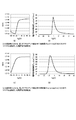
本発明において、チャネル層に上述の積層構成を適用することで、In−Ga−Zn−Oの単層からなるチャネルやIn−Ge−Zn−Oの単層からなるチャネルを用いた場合より、電界効果移動度の大きなTFTを得ることができる。具体的には、In−Ga−Zn−O単層の構成での電界効果移動度は約10cm2/Vsecであるが、本発明の積層構成のチャネルを有したTFTでは20cm2/Vsec以上の電界効果移動度を得ることができる。図4には、本発明のTFTの電界効果移動度がグラフに記されている。
In the present invention, by applying the above-described stacked structure to the channel layer, a channel composed of a single layer of In—Ga—Zn—O or a channel composed of a single layer of In—Ge—Zn—O is used. A TFT having a large field effect mobility can be obtained. Specifically, the field effect mobility in the structure of the In—Ga—Zn—O single layer is about 10
また本発明は、チャネル層に上述の積層構成を適用することで、In−Zn−O単層のチャネルを用いた場合より、組成変動に対する特性変化が小さいTFTを実現できる。本発明者らは、In−Zn−O単層のチャネルを用いた場合は、In:Zn=4:6近傍で良好なスイッチング特性が得られること、特性のIn:Zn比依存性が存在することを報告している。(非特許文献1)。本発明の積層構成を適用することで、より広いIn:Zn比に対して、良好なスイッチング特性を得ることができる。図3にはオンオフ電流比の組成依存性を示した。図3において白三角はIn−Zn−O単層のチャネルを用いた場合であり、黒四角はZn−In−O(第1の層)とZn−In−Ge−O(第2の層)の積層チャネルを用いた場合である。本発明の積層チャネルを用いたTFTの方が、オンオフ電流比の組成依存性が小さいことがわかる。また、広いIn/(In+Zn)値にわたって大きなオン・オフ電流比が得られることがわかる。
上述の効果が得られた理由は、必ずしも明らかではないが以下に考察を述べる。
Further, according to the present invention, by applying the above-described stacked structure to the channel layer, it is possible to realize a TFT whose characteristic change with respect to the composition variation is smaller than that in the case of using an In—Zn—O single layer channel. When the In—Zn—O single layer channel is used, the present inventors can obtain good switching characteristics in the vicinity of In: Zn = 4: 6, and there is an In: Zn ratio dependency of the characteristics. It is reported that. (Non-Patent Document 1). By applying the laminated structure of the present invention, good switching characteristics can be obtained for a wider In: Zn ratio. FIG. 3 shows the composition dependence of the on / off current ratio. In FIG. 3, white triangles are obtained when an In—Zn—O single layer channel is used, and black squares are Zn—In—O (first layer) and Zn—In—Ge—O (second layer). This is a case where the stacked channel is used. It can be seen that the TFT using the laminated channel of the present invention is less dependent on the composition of the on / off current ratio. It can also be seen that a large on / off current ratio can be obtained over a wide range of In / (In + Zn) values.
The reason why the above-described effect is obtained is not necessarily clear, but will be discussed below.
本発明は、電界効果型トランジスタのチャネル層として、特定の組成を有するアモルファス酸化物半導体層を少なくとも2層の積層構成を採用することが重要である。まず、第1のアモルファス酸化物半導体層として電子移動度の高い材料であるZn−In―O膜をゲート絶縁膜に接する側に設ける。当該酸化物半導体層を当該位置に設けることで、大きなオン状態の電流、すなわち大きな電界効果移動度を可能にしていると考えられる。さらに、第2のアモルファス酸化物半導体層としてZn−In―Ge−O膜を前記第1のアモルファス酸化物半導体膜に接して設ける(積層する)ことで、大気や真空などの環境からZn−In−O膜を保護して本来のZn−In−O膜の性能を引き出すことができる。さらに、本発明の積層構成とすることにより良好な界面特性や半導体特性さらには電極−チャネル間の電気接続を可能とし、単層では実現困難作用を実現していると考えることができる。 In the present invention, it is important to employ a laminated structure of at least two amorphous oxide semiconductor layers having a specific composition as a channel layer of a field effect transistor. First, a Zn—In—O film, which is a material having high electron mobility, is provided as a first amorphous oxide semiconductor layer on a side in contact with the gate insulating film. By providing the oxide semiconductor layer at the position, a large on-state current, that is, a large field-effect mobility can be achieved. Further, a Zn—In—Ge—O film is provided as a second amorphous oxide semiconductor layer in contact with the first amorphous oxide semiconductor film (stacked), so that Zn—In can be obtained from an environment such as air or vacuum. The performance of the original Zn—In—O film can be extracted by protecting the —O film. Furthermore, it can be considered that the laminated structure of the present invention enables good interface characteristics, semiconductor characteristics, and electrical connection between the electrode and the channel, and realizes an operation that is difficult to achieve with a single layer.
ここで、本発明の積層構成の特徴的部分を構成する、第2のアモルファス酸化物半導体層に適用するZn−In―Ge(Si)−O膜の特徴について説明する。本発明者らの知見によれば、IV族元素であるGeまたはSiをアモルファス酸化物半導体に添加すると、キャリア濃度を効果的に減じることができる。また、Ga(III族の元素)に比べて、比較的少量のGeまたはSiの添加でキャリア濃度の制御(増加させる又は減少させる)が可能である。さらに、アモルファス酸化物半導体にGeまたはSiを添加することで、抵抗率をはじめとした電気物性の環境(大気、水分など)に対する安定性(外因により変化しにくい)が向上する。 Here, characteristics of the Zn—In—Ge (Si) —O film applied to the second amorphous oxide semiconductor layer, which constitutes a characteristic portion of the stacked structure of the present invention, will be described. According to the knowledge of the present inventors, when Ge or Si which is a group IV element is added to an amorphous oxide semiconductor, the carrier concentration can be effectively reduced. Further, the carrier concentration can be controlled (increased or decreased) by adding a relatively small amount of Ge or Si as compared with Ga (group III element). Further, by adding Ge or Si to the amorphous oxide semiconductor, stability (less likely to change due to external factors) with respect to the electrical property environment (atmosphere, moisture, etc.) including resistivity is improved.
このような特徴を有したIV族元素を添加したアモルファス酸化物半導体と、高移動度という特徴を有したZn−In−O系アモルファス酸化物半導体とを積層させて積層構造とすることが本発明の特徴的部分である。特に、第2のアモルファス酸化物半導体層にZn−In−O系にGeを添加したZn−In−Ge−O系を適用し、Zn−In−O系アモルファス酸化物半導体を適用した構成を選択することで、第1のアモルファス酸化物半導体層と第2のアモルファス酸化物半導体層の間の組成比の差が小さい構成とすることができる。このような構成とすることにより、2つの層の間で物質的な性質の連続性を高め、良質で安定な界面を実現できる。良質な(電気的欠陥の少ない)界面を実現できるために、Zn−In−O系膜の高移動度という特徴を維持したまま、さらに環境に対する安定性や動作安定性に優れたTFTを実現できる。 In the present invention, an amorphous oxide semiconductor added with a group IV element having such characteristics and a Zn-In-O amorphous oxide semiconductor having high mobility are stacked to form a stacked structure. It is a characteristic part. In particular, a configuration in which a Zn-In-Ge-O system in which Ge is added to a Zn-In-O system is applied to the second amorphous oxide semiconductor layer and a Zn-In-O amorphous oxide semiconductor is applied is selected. Thus, the composition ratio difference between the first amorphous oxide semiconductor layer and the second amorphous oxide semiconductor layer can be reduced. By adopting such a configuration, it is possible to increase the continuity of material properties between the two layers and realize a high-quality and stable interface. Since a high quality interface (with few electrical defects) can be realized, a TFT with excellent environmental stability and operational stability can be realized while maintaining the high mobility of the Zn-In-O film. .
本発明の上記チャネル層の積層構成は、単に第1のアモルファス酸化物半導体層を第2のアモルファス酸化物半導体層により物理的に保護するだけでなく、積層構成とすることで電気的特性(デバイス特性)が、単層の場合よりも大きく向上するものである。 The layered structure of the channel layer according to the present invention is not limited to merely physically protecting the first amorphous oxide semiconductor layer with the second amorphous oxide semiconductor layer, but also has a stacked structure to achieve electrical characteristics (devices). Characteristics) are greatly improved as compared with the case of a single layer.
また本発明において、Zn−In−O単層チャネルと同程度の高い電界移動度(例えば20cm2/Vsec)が得られている。このことからも、電界移動度の高い材料であるZn−In―O膜がゲート絶縁膜に接していることで、大きなオン状態の電流、すなわち大きな電界効果移動度を可能にしていると考えることができる。
この結果、上述のように組成変動にともなう特性変化が小さく、さらに特性に優れたTFTが実現できる。
In the present invention, high field mobility (for example, 20 cm 2 / Vsec) comparable to that of a Zn—In—O single layer channel is obtained. From this, it is considered that a large on-state current, that is, a large field-effect mobility is enabled by the contact of the Zn—In—O film, which is a material having a high field mobility, with the gate insulating film. Can do.
As a result, it is possible to realize a TFT having a small characteristic change due to the composition variation as described above and having excellent characteristics.
以下、図面を用いて本発明を実施するための実施の形態を説明する。
図1は、本発明の一実施形態としての薄膜トランジスタの概略を示す断面図である。
図1(a)及び図1(b)において、10は基板、11は本発明の酸化物半導体層からなるチャネル層、12はゲート絶縁層、13はソース電極、14はドレイン電極、15はゲート電極である。11(a)は第1のアモルファス酸化物半導体層、11(b)は第2のアモルファス酸化物半導体層である。
図1(c)では、ゲート絶縁体22である熱酸化SiO2が形成された基板21の上に本発明の酸化物半導体層からなるチャネル層25を配する。23はソース電極、24はドレイン電極である。基板21は、n+−Siからなり、ゲート電極としても機能する。25(a)は第1のアモルファス酸化物半導体層、25(b)は第2のアモルファス酸化物半導体層である。
図1(a)は、半導体チャネル層11の上にゲート絶縁層12とゲート電極15を有するトップゲート構造の例である。図1(b)は、ゲート電極15の上にゲート絶縁層12と半導体チャネル層11を有するボトムゲート構造の例である。図1(c)は、別のボトムゲート型トランジスタの例である。
Hereinafter, embodiments for carrying out the present invention will be described with reference to the drawings.
FIG. 1 is a cross-sectional view schematically showing a thin film transistor as one embodiment of the present invention.
1A and 1B, 10 is a substrate, 11 is a channel layer made of an oxide semiconductor layer of the present invention, 12 is a gate insulating layer, 13 is a source electrode, 14 is a drain electrode, and 15 is a gate. Electrode. 11 (a) is a first amorphous oxide semiconductor layer, and 11 (b) is a second amorphous oxide semiconductor layer.
In FIG. 1C, a
FIG. 1A shows an example of a top gate structure having a
本発明では、TFTの構成は、上記の構造に限定されず、トップゲート又はボトムゲート型、スタガ型、逆スタガ型、コープレナ−型、逆コープレナ−型などの任意の構造に適用できる。 In the present invention, the structure of the TFT is not limited to the above structure, and can be applied to any structure such as a top gate or bottom gate type, a stagger type, an inverted stagger type, a coplanar type, and an inverse coplanar type.
電界効果型トランジスタは、ゲート電極15、ソース電極13及びドレイン電極14を有する3端子デバイスである。電界効果型トランジスタは、電圧VGをゲート電極へ印加すると、チャネル層を通って流れるドレイン電流IDを制御することができ、ソース電極とドレイン電極との間を流れる電流を制御する電子デバイスである。
以下各層について説明する。
The field effect transistor is a three-terminal device having a
Each layer will be described below.
(チャネル層)
本発明の薄膜トランジスタは、チャネル層が第1のアモルファス酸化物半導体層11(a)と第2のアモルファス酸化物半導体層11(b)との積層構成からなること、さらにはそれぞれの層の材料に特徴がある。本発明において、第1のアモルファス酸化物半導体層11(a)はゲート絶縁層12と第2のアモルファス酸化物半導体層11(b)との間に、ゲート絶縁層12に接して設けられる。
(Channel layer)
In the thin film transistor of the present invention, the channel layer has a laminated structure of the first amorphous oxide semiconductor layer 11 (a) and the second amorphous oxide semiconductor layer 11 (b), and further, the material of each layer is There are features. In the present invention, the first amorphous oxide semiconductor layer 11 (a) is provided in contact with the
また前記第2のアモルファス酸化物半導体層の一部がソース電極またはドレイン電極と前記第1のアモルファス酸化物半導体層との間に設けることができる。 A part of the second amorphous oxide semiconductor layer may be provided between the source electrode or the drain electrode and the first amorphous oxide semiconductor layer.
本発明の第1のアモルファス酸化物半導体層11(a)は、ZnまたはInから選択される少なくとも1つの元素を含むアモルファス酸化物半導体層からなる。特に、ZnとInとの両元素を含有するアモルファス酸化物(アモルファスZn−In−O)が好適である。他にも、アモルファスIn−Sn−O、アモルファスIn−O、アモルファスIn−Ge−O、アモルファスZn−Sn−O、アモルファスIn−Zn−Ga−O、などを好適に用いることができる。 The first amorphous oxide semiconductor layer 11 (a) of the present invention is composed of an amorphous oxide semiconductor layer containing at least one element selected from Zn or In. In particular, an amorphous oxide (amorphous Zn—In—O) containing both elements of Zn and In is suitable. In addition, amorphous In—Sn—O, amorphous In—O, amorphous In—Ge—O, amorphous Zn—Sn—O, amorphous In—Zn—Ga—O, and the like can be preferably used.
本発明において第1のアモルファス酸化物半導体の組成比としては、当該第1のアモルファス酸化物半導体層に含まれるZnの組成比Zn/(In+Zn)が0.3以上、0.75未満が好ましい。 In the present invention, the composition ratio of the first amorphous oxide semiconductor is preferably such that the composition ratio Zn / (In + Zn) of Zn contained in the first amorphous oxide semiconductor layer is 0.3 or more and less than 0.75.
本発明の第2のアモルファス酸化物半導体層11(b)としては、GeまたはSiから選択される少なくとも1つの元素と、ZnまたはInから選択される少なくとも1つの元素と、を含むアモルファス酸化物からなる。特にZn,In,Geを全て含有するアモルファス酸化物(アモルファスZn−In−Ge−O)が好適である。他にも、Zn−In−Si−O,Zn−Sn−Ge−O、In−Ge−O、Zn−Ge−O、In−Sn−Ge−Oなどを好適に用いることができる。 As the second amorphous oxide semiconductor layer 11 (b) of the present invention, an amorphous oxide containing at least one element selected from Ge or Si and at least one element selected from Zn or In is used. Become. In particular, an amorphous oxide containing all of Zn, In, and Ge (amorphous Zn—In—Ge—O) is preferable. In addition, Zn—In—Si—O, Zn—Sn—Ge—O, In—Ge—O, Zn—Ge—O, In—Sn—Ge—O, and the like can be preferably used.
本発明の第1のアモルファス酸化物半導体層11(a)と第2のアモルファス酸化物半導体層11(b)とは組成が異なる材料で構成することにより、各アモルファス酸化物半導体層が相乗的に機能することで本発明の効果を奏する。 By configuring the first amorphous oxide semiconductor layer 11 (a) and the second amorphous oxide semiconductor layer 11 (b) of the present invention with materials having different compositions, each amorphous oxide semiconductor layer is synergistically formed. By functioning, the effect of the present invention is achieved.
本発明において上記第1及び第2のアモルファス酸化物は、当該酸化物に含まれる全ての元素の中で酸素を最も多く含有し、次いで上記した各元素が含まれる。そして半導体特性に悪影響を与えない限り上記した元素以外の他の元素を不純物として含み得る。 In the present invention, the first and second amorphous oxides contain the largest amount of oxygen among all the elements contained in the oxide, and then each of the elements described above. As long as the semiconductor characteristics are not adversely affected, other elements than the above elements can be included as impurities.
例えばZn−In−Ge−Oからなるアモルファス酸化物は、全ての元素の中で酸素を最も多く含有し、2番目に亜鉛(もしくはインジウム)、3番目にインジウム(もしくは亜鉛)、4番目にゲルマニウムを多く含有する。本発明の第2のアモルファス酸化物半導体層に含まれるGeの組成比Ge/(In+Zn+Ge)は、0.01以上0.4以下が好ましい。さらに好ましくはGe/(In+Zn+Ge)が、0.03以上0.15以下である。 For example, an amorphous oxide made of Zn—In—Ge—O contains the largest amount of oxygen among all the elements, secondly zinc (or indium), thirdly indium (or zinc), fourthly germanium. Contains a lot. The composition ratio Ge / (In + Zn + Ge) of Ge contained in the second amorphous oxide semiconductor layer of the present invention is preferably 0.01 or more and 0.4 or less. More preferably, Ge / (In + Zn + Ge) is 0.03 or more and 0.15 or less.
このような積層チャネル構造と各層の材料の組み合わせを用いることで、電気的特性に優れ、且つ、素子特性の組成変動が小さいTFTを実現できる。 By using such a combination of the laminated channel structure and the material of each layer, it is possible to realize a TFT having excellent electrical characteristics and small composition fluctuations in element characteristics.
本発明において第1のアモルファス酸化物半導体層11(a)の膜厚は、10nm以上、50nm以下とすることが好ましい。10nm以上の膜厚とすることでより大きな電流でTFT動作を安定して行うことができる。一方、膜厚が厚すぎるとノーマリオフのTFTを実現することが難しくなることから、膜厚の上限についてより好ましくは30nm以下とすることが好ましい。 In the present invention, the thickness of the first amorphous oxide semiconductor layer 11 (a) is preferably 10 nm or more and 50 nm or less. By setting the film thickness to 10 nm or more, TFT operation can be stably performed with a larger current. On the other hand, if the film thickness is too thick, it becomes difficult to realize a normally-off TFT. Therefore, the upper limit of the film thickness is preferably set to 30 nm or less.
また第2のアモルファス酸化物半導体層11(b)の膜厚は、10nm以上、50nm以下とすることが好ましい。 The film thickness of the second amorphous oxide semiconductor layer 11 (b) is preferably 10 nm or more and 50 nm or less.
第2のアモルファス酸化物半導体層11(b)の膜厚は、10nm以上とすることで、第1のアモルファス酸化物半導体を保護し、環境に対する安定性を高める作用を機能させることができる。また、図1(b)、(c)の構成のように、第2のアモルファス酸化物半導体層の一部がソース電極またはドレイン電極と第1のアモルファス酸化物半導体層との間に設けられる構成においては、前記膜厚の上限はより好ましくは30nm以下である。30nm以下の膜厚とすることにより、電極と第1のアモルファス酸化物半導体層の間で十分な電気的な接続を得ることができる。 By setting the film thickness of the second amorphous oxide semiconductor layer 11 (b) to 10 nm or more, the first amorphous oxide semiconductor can be protected and the function of improving the stability to the environment can be functioned. 1B and 1C, a part of the second amorphous oxide semiconductor layer is provided between the source electrode or the drain electrode and the first amorphous oxide semiconductor layer. The upper limit of the film thickness is more preferably 30 nm or less. By setting the thickness to 30 nm or less, sufficient electrical connection can be obtained between the electrode and the first amorphous oxide semiconductor layer.
本発明において、第1のアモルファス酸化物半導体層11(a)に適用するアモルファス酸化物半導体膜は、抵抗率が10−1Ωcm〜105(Ωcm)の範囲の薄膜を用いることができる。キャリア濃度としては1014〜1020(1/cm3)の範囲の材料を適用できる。電子移動度は10cm2/Vsecよりも大きいことが好ましい。 In the present invention, the amorphous oxide semiconductor film applied to the first amorphous oxide semiconductor layer 11 (a) can be a thin film having a resistivity in the range of 10 −1 Ωcm to 10 5 (Ωcm). A carrier concentration in the range of 10 14 to 10 20 (1 / cm 3 ) can be applied. The electron mobility is preferably greater than 10 cm 2 / Vsec.
第2のアモルファス酸化物半導体層11(b)に適用するアモルファス酸化物半導体膜は、抵抗率が101Ωcm〜107(Ωcm)の範囲の薄膜を用いることができる。キャリア濃度としては1012〜1018(1/cm3)の範囲の材料を適用できる。より好ましくは1016(1/cm3)以下である。第2のアモルファス酸化物半導体層のキャリア濃度を小さくすることで、ノーマリオフ型のトランジスタを実現できる。電子移動度は0.1cm2/Vsecよりも大きいことが好ましく、より好ましくは1cm2/Vsec以上である。 As the amorphous oxide semiconductor film applied to the second amorphous oxide semiconductor layer 11 (b), a thin film having a resistivity in the range of 10 1 Ωcm to 10 7 (Ωcm) can be used. A carrier concentration in the range of 10 12 to 10 18 (1 / cm 3 ) can be applied. More preferably, it is 10 16 (1 / cm 3 ) or less. A normally-off transistor can be realized by reducing the carrier concentration of the second amorphous oxide semiconductor layer. The electron mobility is preferably greater than 0.1 cm 2 / Vsec, more preferably 1 cm 2 / Vsec or more.
本発明において、第1のアモルファス酸化物半導体層11(a)を構成する材料の電子移動度が、第2のアモルファス酸化物半導体層11(b)を構成する材料の電子移動度よりも大きいことが好ましい。このように電子移動度の大きい材料をゲート絶縁層に接して配することで、電界効果移動度の大きなTFTを実現することができる。
また、第2のアモルファス酸化物半導体層11(b)を構成する材料のキャリア濃度が、第1のアモルファス酸化物半導体層11(a)を構成する材料のキャリア濃度よりも小さいことが好ましい。このようにキャリア濃度の小さい材料を、ゲート絶縁層から離れた側に配することで、環境安定性や駆動安定性に優れたTFTを実現することができる。
また、図1(b)や図1(c)の構成のように、第2のアモルファス酸化物半導体層の一部がソース電極またはドレイン電極と第1のアモルファス酸化物半導体層との間に設けられる構成においては、電極と第1のアモルファス酸化物半導体層の間で十分な電気的な接続がなされることが好ましい。このような構成においては、第2のアモルファス酸化物半導体層11(b)の材料の抵抗率を105(Ωcm)以下とすることが好ましい。このような構成とすることで、良好な電気接続を得ることができる。
In the present invention, the electron mobility of the material constituting the first amorphous oxide semiconductor layer 11 (a) is larger than the electron mobility of the material constituting the second amorphous oxide semiconductor layer 11 (b). Is preferred. By arranging a material having a high electron mobility in contact with the gate insulating layer in this manner, a TFT having a high field effect mobility can be realized.
The carrier concentration of the material forming the second amorphous oxide semiconductor layer 11 (b) is preferably smaller than the carrier concentration of the material forming the first amorphous oxide semiconductor layer 11 (a). By disposing the material having a low carrier concentration on the side away from the gate insulating layer, a TFT having excellent environmental stability and driving stability can be realized.
In addition, as in the structures of FIGS. 1B and 1C, part of the second amorphous oxide semiconductor layer is provided between the source electrode or the drain electrode and the first amorphous oxide semiconductor layer. In such a configuration, it is preferable that sufficient electrical connection is made between the electrode and the first amorphous oxide semiconductor layer. In such a configuration, the resistivity of the material of the second amorphous oxide semiconductor layer 11 (b) is preferably 10 5 (Ωcm) or less. With such a configuration, a good electrical connection can be obtained.
本発明のTFTにおける好ましい積層チャネル構造として、第1のアモルファス酸化物半導体層にアモルファスZn−In−O系膜を配し、第2のアモルファス酸化物半導体層にアモルファスZn−In−Ge(もしくはSi)―O系膜を配した構造が挙げられる。以下に、本発明の積層チャネル構造おいて好ましい金属組成比について詳しく説明する。 As a preferable stacked channel structure in the TFT of the present invention, an amorphous Zn-In-O-based film is disposed on the first amorphous oxide semiconductor layer, and amorphous Zn-In-Ge (or Si) is disposed on the second amorphous oxide semiconductor layer. ) -O-based film is included. Hereinafter, a preferable metal composition ratio in the laminated channel structure of the present invention will be described in detail.
第1のアモルファス酸化物半導体層11(a)にIn−Zn−O薄膜を用いる場合、Zn/(In+Zn)で表されるZnの原子組成比率が、0.75以上で結晶、あるいは結晶性が高くなる。このような場合、多結晶粒子界面の散乱により、電子移動度を大きくすることができないと考えられる。かつ電気的特性を考慮すると、Znの原子組成比Zn/(In+Zn)が前述のように0.3以上0.75未満の薄膜を用いることが好ましい。
但し,後で実施例にも示すが、ノーマリーオン型の高移動度TFT作製には、第1のアモルファス酸化物半導体層におけるZnの原子組成比率から0.4未満にすることが好ましい。
When an In—Zn—O thin film is used for the first amorphous oxide semiconductor layer 11 (a), the atomic composition ratio of Zn represented by Zn / (In + Zn) is 0.75 or more, and crystal or crystallinity is obtained. Get higher. In such a case, it is considered that the electron mobility cannot be increased due to scattering at the interface of the polycrystalline particles. In consideration of electrical characteristics, it is preferable to use a thin film having an atomic composition ratio Zn / (In + Zn) of 0.3 to less than 0.75 as described above.
However, as will be described later in Examples, for the preparation of a normally-on type high mobility TFT, it is preferable that the atomic composition ratio of Zn in the first amorphous oxide semiconductor layer is less than 0.4.
また、第2のアモルファス酸化物半導体層11(b)にZn−In−Ge−O薄膜を用いる場合、Geの原子組成比Ge/(In+Zn+Ge)が大きくなると高抵抗になり、チャネルと電極間の抵抗が大きくなり好ましくない。加えて、広いIn/Zn組成比で良好なTFT動作が可能となる組成を考慮すると、前述のようにGe/(In+Zn+Ge)が0.01以上0.4以下の値の薄膜を用いることが好ましい。更には,Ge/(In+Zn+Ge)が0.03以上0.15以下の薄膜を用いることはより好ましい。 Further, in the case where a Zn—In—Ge—O thin film is used for the second amorphous oxide semiconductor layer 11 (b), when the atomic composition ratio Ge / (In + Zn + Ge) of Ge is increased, the resistance is increased, and the channel and the electrode are separated. Resistance becomes large, which is not preferable. In addition, considering a composition that enables a good TFT operation with a wide In / Zn composition ratio, it is preferable to use a thin film having a value of Ge / (In + Zn + Ge) of 0.01 or more and 0.4 or less as described above. . Furthermore, it is more preferable to use a thin film having Ge / (In + Zn + Ge) of 0.03 or more and 0.15 or less.
また、第1のアモルファス酸化物半導体層に含まれるZnの組成比 Zn/(In+Zn)と前記第2のアモルファス酸化物半導体層に含まれるZnの組成比 Zn/(In+Zn)が同一である構成は、好適な構成の一つである。このような構成は、2つの層の間の物質的性質(価電子帯上端、伝導帯下端の深さなど)の連続性に優れた積層構造が期待できる。また、このような積層構造では、良好な界面の形成が期待できるからである。特に、図1(b)や図1(c)の構成のように、第2のアモルファス酸化物半導体層の一部がソース電極またはドレイン電極と第1のアモルファス酸化物半導体層との間に設けられる構成においては、電極と第1のアモルファス酸化物半導体層の間で十分な電気的な接続がなされることが好ましい。このような構成においては、第1のアモルファス酸化物半導体層と第2のアモルファス酸化物半導体層の間の電気接続が良好であることが好ましく、第1のアモルファス酸化物半導体層と第2のアモルファス酸化物半導体層の伝導帯下端が近いことが好ましい。このような構成において、上述の11(b)の材料の抵抗率を105(Ωcm)以下とすることが好ましい。このような構成において、2つの層のZn/(In+Zn)が同一である構成は、良好な電気接続を可能としうる。 The composition ratio Zn / (In + Zn) contained in the first amorphous oxide semiconductor layer is the same as the Zn composition ratio Zn / (In + Zn) contained in the second amorphous oxide semiconductor layer. This is one of the preferred configurations. Such a structure can be expected to have a laminated structure with excellent continuity of material properties (the upper end of the valence band, the depth of the lower end of the conduction band, etc.) between the two layers. Moreover, it is because formation of a favorable interface can be expected in such a laminated structure. In particular, as shown in FIGS. 1B and 1C, a part of the second amorphous oxide semiconductor layer is provided between the source or drain electrode and the first amorphous oxide semiconductor layer. In such a configuration, it is preferable that sufficient electrical connection is made between the electrode and the first amorphous oxide semiconductor layer. In such a structure, it is preferable that the electrical connection between the first amorphous oxide semiconductor layer and the second amorphous oxide semiconductor layer is good, and the first amorphous oxide semiconductor layer and the second amorphous oxide semiconductor layer are preferable. The lower end of the conduction band of the oxide semiconductor layer is preferably close. In such a configuration, it is preferable that the resistivity of the above-described material 11 (b) is 10 5 (Ωcm) or less. In such a configuration, a configuration in which the Zn / (In + Zn) of the two layers is the same can enable good electrical connection.
他にも、製造上の利点がある。たとえば、第1のアモルファス酸化物半導体層を形成する際にはZnOとIn2O3を混合したセラミックからなる材料源(スパッタターゲット)を用い、第2のアモルファス酸化物半導体層を形成する際には上述の材料源とGeからなる材料源を用いた同時成膜を行うことがあげられる。このような手法を用いると、2つの層を連続して成膜することができ、さらに組成を容易に調整することができる。このように連続製膜する際には、第1のアモルファス酸化物半導体層を形成する第1の工程と、第2のアモルファス酸化物半導体層を形成する第2の工程までを通して装置内の真空度が300Pa以下、好ましくは100Pa以下に保持することで、層間の界面を清浄なものとすることができる。 There are other manufacturing advantages. For example, when forming the first amorphous oxide semiconductor layer, a material source (sputter target) made of a ceramic in which ZnO and In 2 O 3 are mixed is used to form the second amorphous oxide semiconductor layer. The simultaneous film formation using the above-mentioned material source and the material source made of Ge can be mentioned. When such a method is used, two layers can be continuously formed, and the composition can be easily adjusted. In such continuous film formation, the degree of vacuum in the apparatus is passed through the first step of forming the first amorphous oxide semiconductor layer and the second step of forming the second amorphous oxide semiconductor layer. Is maintained at 300 Pa or less, preferably 100 Pa or less, the interface between the layers can be made clean.
さらには、2つの材料の組成が近いということは、それぞれの層の間での元素混合汚染(クロスコンタミ)が生じにくいという利点からも、好ましい構成である。 Furthermore, the fact that the compositions of the two materials are close to each other is a preferable configuration because of the advantage that element mixed contamination (cross-contamination) does not easily occur between the respective layers.
また、前述の通り、本発明者らの知見によればIn−Zn−O単層チャネルTFTにおいて、Zn/(In+Zn)で表されるZnの原子組成比率が0.6近傍で良好なスイッチング特性が得られる。そして、このような組成のIn−Zn−O薄膜を第2のアモルファス酸化物半導体層11(b)に用い、Zn/(In+Zn)が0.6より小さい薄膜を第1のアモルファス酸化物半導体層に用いることも有効である。 As described above, according to the knowledge of the present inventors, in the In—Zn—O single layer channel TFT, good switching characteristics are obtained when the atomic composition ratio of Zn represented by Zn / (In + Zn) is around 0.6. Is obtained. Then, an In—Zn—O thin film having such a composition is used for the second amorphous oxide semiconductor layer 11 (b), and a thin film having Zn / (In + Zn) smaller than 0.6 is used as the first amorphous oxide semiconductor layer. It is also effective to use it.
また、本発明のチャネル層は、少なくとも第1および第2のアモルファス酸化物半導体層を有しておれば良く、付加的に別の層を設けることも許容する。すなわち、多層チャネルとしてもよい。 Further, the channel layer of the present invention only needs to have at least the first and second amorphous oxide semiconductor layers, and it is allowed to additionally provide another layer. That is, a multilayer channel may be used.
また本発明においては、第1のアモルファス酸化物半導体層として少なくともZnとInを含む材料を選択し、第2のアモルファス酸化物半導体層として少なくともZnとInとGeを含む材料を選択した際の組成比の調整は以下の方法も好ましい。即ち、第1及び第2のアモルファス酸化物半導体層のInとZnに対する組成比(Zn/(In+Zn))は同一になるようにターゲット材料の組成比等を調整する。典型的には同一の組成比を有するZnとInとからなるターゲット材料を使用する。そして第2のアモルファス酸化物半導体層のみさらにGeのターゲットを併用することで当該アモルファス酸化物半導体層中の組成比を調整する。このように第1及び第2のアモルファス酸化物半導体層の各々に含まれるInとZnのみに着目した際にこれらの各層のZnの組成比Zn/(In+Zn)を同一とすることで、組成比の調整をより容易にすることができる。 Further, in the present invention, a composition obtained when a material containing at least Zn and In is selected as the first amorphous oxide semiconductor layer and a material containing at least Zn, In and Ge is selected as the second amorphous oxide semiconductor layer. The following method is also preferable for adjusting the ratio. That is, the composition ratio of the target material and the like are adjusted so that the composition ratio (Zn / (In + Zn)) of In and Zn of the first and second amorphous oxide semiconductor layers is the same. Typically, a target material composed of Zn and In having the same composition ratio is used. The composition ratio in the amorphous oxide semiconductor layer is adjusted by using a Ge target in combination with only the second amorphous oxide semiconductor layer. Thus, when focusing only on In and Zn contained in each of the first and second amorphous oxide semiconductor layers, the Zn composition ratio Zn / (In + Zn) of these layers is made the same, thereby making the composition ratio Can be adjusted more easily.
また、本発明において上記「組成比が同一」とは、組成比が実質的に同一であることを意味する。即ち組成比が全く同一である場合だけでなく、誤差の範囲での組成比に違いがある場合も含む。本発明者らの知見によれば組成比に違いがあってもその違いが3%以内、好ましくは1%以内であれば本発明の効果を奏する。 In the present invention, the above-mentioned “composition ratio is the same” means that the composition ratio is substantially the same. That is, it includes not only the case where the composition ratio is exactly the same, but also the case where there is a difference in the composition ratio within the error range. According to the knowledge of the present inventors, even if there is a difference in composition ratio, the effect of the present invention is exhibited if the difference is within 3%, preferably within 1%.
本発明において第1のアモルファス酸化物半導体層を形成する工程(第1の工程)と第2のアモルファス酸化物半導体を形成する工程(第2の工程)を連続して行う際には、以下の条件を満たすことが好ましい。即ち本発明者らの知見によれば、第1の工程と第2の工程を通して、当該アモルファス酸化物半導体層を形成する装置内部(成膜室、搬送経路等を含む)の圧力を所定の範囲内に維持することが好ましい。具体的には300Pa以下の真空雰囲気に維持することで、アモルファス酸化物半導体膜の形成中に当該膜の特性が変化又は劣化することを抑制することができる。また、本発明において前記圧力はさらに好ましくは100Pa以下の真空雰囲気に維持することが本発明においては有効である。 In the present invention, when the step of forming the first amorphous oxide semiconductor layer (first step) and the step of forming the second amorphous oxide semiconductor (second step) are successively performed, It is preferable to satisfy the conditions. That is, according to the knowledge of the present inventors, the pressure inside the apparatus for forming the amorphous oxide semiconductor layer (including the film formation chamber and the transfer path) is set within a predetermined range through the first step and the second step. It is preferable to maintain within. Specifically, by maintaining the vacuum atmosphere at 300 Pa or less, it is possible to suppress change or deterioration of characteristics of the film during formation of the amorphous oxide semiconductor film. In the present invention, the pressure is more preferably maintained in a vacuum atmosphere of 100 Pa or less.
また、第1の工程と第2の工程を通して上記のように真空雰囲気に維持する代わりに、不活性ガス雰囲気中に維持することによっても同様の効果を得ることができる。不活性ガスとしては、He、Ne、Ar等が好ましいが、これ以外のガスであってもアモルファス酸化物半導体膜に悪影響を与えないガスであれば用いることができる。不活性ガス雰囲気の圧力としては、特に制限はないが、大気圧以下であれば本発明の効果を得ることができ、より好ましくは1000Pa以下、さらに好ましくは500Pa以下である。 Further, the same effect can be obtained by maintaining in an inert gas atmosphere instead of maintaining the vacuum atmosphere as described above through the first step and the second step. As the inert gas, He, Ne, Ar, or the like is preferable. However, other gases can be used as long as they do not adversely affect the amorphous oxide semiconductor film. Although there is no restriction | limiting in particular as the pressure of an inert gas atmosphere, The effect of this invention can be acquired if it is atmospheric pressure or less, More preferably, it is 1000 Pa or less, More preferably, it is 500 Pa or less.
ここではZn−In−Ge−O系薄膜を第2のアモルファス酸化物半導体層に適用する構成について述べたが、Zn−In−O系膜を第2のアモルファス酸化物半導体層に適用することも、好適な例の一つである。本発明者らの知見によれば、In−Zn−O系薄膜は、Zn/(In+Zn)で表されるZnの原子組成比率Zn/(In+Zn)が0.6近傍で良好な環境安定性を示す。たとえば、このような組成のIn−Zn−O薄膜は第2のアモルファス酸化物半導体層11(b)として好適な一例である。 Although the structure in which the Zn—In—Ge—O-based thin film is applied to the second amorphous oxide semiconductor layer is described here, the Zn—In—O-based film may be applied to the second amorphous oxide semiconductor layer. This is one of the preferred examples. According to the knowledge of the present inventors, the In—Zn—O-based thin film has good environmental stability when the atomic composition ratio Zn / (In + Zn) of Zn represented by Zn / (In + Zn) is around 0.6. Show. For example, an In—Zn—O thin film having such a composition is a suitable example for the second amorphous oxide semiconductor layer 11 (b).
Zn/(In+Zn)が0.6より小さいIn−Zn−O系薄膜を第1のアモルファス酸化物半導体層に用い、Zn/(In+Zn)が0.6近傍のIn−Zn−O系薄膜をアモルファス酸化物半導体層に用いる構成も、有効な構成の一つである。 An In—Zn—O-based thin film whose Zn / (In + Zn) is smaller than 0.6 is used for the first amorphous oxide semiconductor layer, and an In—Zn—O-based thin film whose Zn / (In + Zn) is near 0.6 is amorphous. A structure used for the oxide semiconductor layer is also an effective structure.
上述のチャネル構成においては、組成の異なる2つの材料からなる積層構造となっているが、2層の構造に限らず任意の層数を有した多層チャネル構造としてもよい。 In the above-described channel configuration, a laminated structure made of two materials having different compositions is used. However, the channel structure is not limited to a two-layer structure, and may be a multilayer channel structure having an arbitrary number of layers.
すなわち、本発明のチャネル層は、少なくとも上述の第1のアモルファス酸化物半導体層および第2のアモルファス酸化物半導体層を有しておれば良く、3層以上の任意の積層構成としてもよい。たとえば、Zn−In−O膜からなる第1のアモルファス酸化物半導体層、Zn−In−Ge−O膜からなる第2層、Zn−In−Si−O膜からなる第3層を有した3層チャネル構造の構成や、Zn−In−O膜からなる第1のアモルファス酸化物半導体層、Zn−In−Ge−O膜からなる第2層、Zn−In−O膜からなる第3の層、Zn−In−Ge−O膜からなる第4層を有した4層チャネル構造の構成などが挙げられる。 That is, the channel layer of the present invention only needs to include at least the first amorphous oxide semiconductor layer and the second amorphous oxide semiconductor layer described above, and may have an arbitrary stacked structure of three or more layers. For example, 3 having a first amorphous oxide semiconductor layer made of a Zn—In—O film, a second layer made of a Zn—In—Ge—O film, and a third layer made of a Zn—In—Si—O film. Layer channel structure configuration, first amorphous oxide semiconductor layer made of Zn—In—O film, second layer made of Zn—In—Ge—O film, third layer made of Zn—In—O film And a configuration of a four-layer channel structure having a fourth layer made of a Zn—In—Ge—O film.
また、上述のチャネル構成においては、組成の異なる2つの材料からなる積層構造からなっているが、厚さ方向で連続的に組成が変化した構成であっても良い。たとえば、膜厚方向で、Zn−In−O膜の組成からZn−In−Ge−O膜の組成となるようにGe(Si)の含有量が連続的に増えていく構成があげられる。 Further, although the above-described channel configuration has a laminated structure made of two materials having different compositions, a configuration in which the composition is continuously changed in the thickness direction may be used. For example, there is a configuration in which the content of Ge (Si) continuously increases in the film thickness direction so that the composition of the Zn—In—O film becomes the composition of the Zn—In—Ge—O film.
上述したような積層チャネル構造と各層の材料の組み合わせを用いることで、電気的特性に優れ、且つ、素子特性の組成変動が小さいTFTを作製することができる。 By using a combination of the laminated channel structure and the material of each layer as described above, it is possible to manufacture a TFT that has excellent electrical characteristics and small composition variation in element characteristics.
(ゲート絶縁層)
本発明においてゲート絶縁層12として、シリコン酸化物SiOx又は窒素化シリコンSiNx及びシリコンオキシナイトライドSiOxNyを好適に用いることができる。また本発明のゲート絶縁層として用いることができるシリコン以外の酸化物としては、GeO2、Al2O3、Ga2O3、Y2O3及びHfO2等が挙げられる。
これらの中でもSiOxは、CVD法によって良質な膜を容易に形成できるため好ましい。TFTの安定性もSiOxを用いた際に良好である。
本発明においては、優れた絶縁特性を有する薄膜ゲート絶縁物を利用することによって、ソース−ゲート及びドレイン−ゲート電極間リーク電流を約10−12Aに調節することができる。
本発明においてゲート絶縁層の厚さは、50〜300nmが好ましい。
(Gate insulation layer)
In the present invention, silicon oxide SiOx or silicon nitride SiNx and silicon oxynitride SiO x N y can be suitably used as the
Among these, SiOx is preferable because a high-quality film can be easily formed by a CVD method. The stability of TFT is also good when SiOx is used.
In the present invention, the leak current between the source-gate and drain-gate electrodes can be adjusted to about 10 −12 A by using a thin film gate insulator having excellent insulation characteristics.
In the present invention, the thickness of the gate insulating layer is preferably 50 to 300 nm.
(電極)
本発明においてソース電極13、ドレイン電極14及びゲート電極15の材料は高い導電率を有する材料を用いることが好ましい。本発明においてはPt又はAu、Ni、W、Mo及びAgなどの金属電極を用いることが好ましい。又、酸化インジウム錫(ITO)及びZnOなどの透明導電膜も用いてよい。また本発明に用いる電極の構造としては、単層構造でも良いが、Au及びTi等の複数の層のカスケード構造としてもよい。
(electrode)
In the present invention, the
(基板)
ガラス基板、プラスチック基板及びプラスチックフィルム等の樹脂材料を基板10として用いてよい。
本発明において上記チャネル層及びゲート絶縁層は、可視光に対して透明にすることができる。
したがって、用いられる電極を可視光に対して透明な材料を選択することによって、可視光域で全体が透明な薄膜トランジスタを作り出すことが可能である。
(substrate)
A resin material such as a glass substrate, a plastic substrate, and a plastic film may be used as the
In the present invention, the channel layer and the gate insulating layer can be transparent to visible light.
Therefore, by selecting a material that is transparent to visible light as the electrode used, it is possible to create a thin film transistor that is entirely transparent in the visible light range.
(製造方法)
チャネル層の成膜の方法として、スパッタリング法(SP法)、パルスレーザ蒸着法(PLD法)、電子ビーム蒸着法(EB法)及び原子層蒸着法などの気相蒸着法を用いると好ましい。気相蒸着法の中で、大量生産性を考慮するとSP法が適当である。しかし、膜形成法は、これらの方法に限定されない。
(Production method)
As a method for forming the channel layer, it is preferable to use a vapor deposition method such as a sputtering method (SP method), a pulse laser deposition method (PLD method), an electron beam deposition method (EB method), or an atomic layer deposition method. Among vapor phase deposition methods, the SP method is appropriate in view of mass productivity. However, the film forming method is not limited to these methods.
本発明の製造工程においては、意図的な加熱をまったく行わずに基板の温度を室温に保持して成膜することができる。この技法によれば、プラスチック基板上の透明薄膜トランジスタの低温作製プロセスが可能になる。 In the production process of the present invention, the film can be formed while maintaining the temperature of the substrate at room temperature without any intentional heating. This technique allows a low temperature fabrication process for transparent thin film transistors on plastic substrates.
本発明のTFTが示す特性は、駆動力が高い(電流量が大きい)為、OLED(有機LED)の駆動用のTFTにとって非常に望ましい特性である。 The characteristics of the TFT of the present invention are very desirable for TFTs for driving OLEDs (organic LEDs) because of their high driving power (large amount of current).
このような薄膜トランジスタを配した半導体装置(アクティブマトリックス基板)は、透明な基板とアモルファス酸化物TFTを用いているため、表示装置に適用した際にその開口率を増やすことができる。 Since a semiconductor device (active matrix substrate) provided with such a thin film transistor uses a transparent substrate and an amorphous oxide TFT, the aperture ratio can be increased when applied to a display device.
特に、有機ELディスプレイに用いる際には、基板側からも光を取り出す構成(ボトムエミッション)を採用することが可能となる。 In particular, when used in an organic EL display, it is possible to adopt a configuration (bottom emission) in which light is extracted also from the substrate side.
本実施形態の半導体装置は、IDタグ又はICタグなどのさまざまな用途に用いることが考えられる。 The semiconductor device of this embodiment can be used for various applications such as an ID tag or an IC tag.
以下、具体的に、本実施形態の電界効果型トランジスタを配した半導体装置の一例として表示装置を詳細に説明する。 In the following, a display device will be described in detail as an example of a semiconductor device in which the field effect transistor of this embodiment is arranged.
本実施形態の電界効果型トランジスタの出力端子であるドレイン電極に、有機又は無機のエレクトロルミネッセンス(EL)素子、液晶素子等の表示素子の電極に接続することで表示装置を構成することができる。以下に、表示装置の断面図を用いて具体的な表示装置構成の例を説明する。 A display device can be configured by connecting a drain electrode which is an output terminal of the field effect transistor of the present embodiment to an electrode of a display element such as an organic or inorganic electroluminescence (EL) element or a liquid crystal element. Hereinafter, an example of a specific display device configuration will be described using a cross-sectional view of the display device.
図7に示すように、基体111上に、チャネル層112と、ソース電極113と、ドレイン電極114とゲート絶縁膜115と、ゲート電極116から構成される電界効果型トランジスタを形成する。ここで、図7および図8では簡単のため、チャネル層を1層に表記しているが、前述のように積層構成からなるものとする。そして、ドレイン電極114に、層間絶縁層117を介して電極118が接続されており、電極118は発光層119と接し、さらに発光層119が電極120と接している。かかる構成により、発光層119に注入する電流を、ソース電極113からドレイン電極114に、チャネル層112に形成されるチャネルを介して流れる電流値によって制御することが可能となる。したがって、これを電界効果型トランジスタのゲート電極116の電圧によって制御することができる。ここで、電極118、発光層119、電極120は無機若しくは有機のエレクトロルミネッセンス素子を構成する。
As shown in FIG. 7, a field effect transistor including a
また別の構成としては、図8に示すように、ドレイン電極114が延長されて電極118を兼ねており、これを高抵抗膜121、122に挟まれた液晶セルや電気泳動型粒子セル123へ電圧を印加する電極118とする構成を取ることもできる。液晶セルや電気泳動型粒子セル123、高抵抗層121及び122、電極118、電極120は表示素子を構成する。これら表示素子に印加する電圧を、ソース電極113からドレイン電極114にチャネル層112に形成されるチャネルを介して流れる電流値によって制御することが可能となる。したがって、これをTFTのゲート電極116の電圧によって制御することができる。ここで表示素子の表示媒体が流体と粒子を絶縁性被膜中に封止したカプセルであるなら、高抵抗膜121、122は不要である。
As another configuration, as shown in FIG. 8, the
上述の2例において薄膜トランジスタとしては、スタガ構造(トップゲート型)の構成で代表させたが、本発明は必ずしも本構成に限定されるものではない。例えば、薄膜トランジスタの出力端子であるドレイン電極と表示素子の接続が位相幾何的に同一であれば、コプレナー型等他の構成も可能である。 In the above two examples, the thin film transistor is represented by a staggered structure (top gate type), but the present invention is not necessarily limited to this structure. For example, other configurations such as a coplanar type are possible if the connection between the drain electrode, which is the output terminal of the thin film transistor, and the display element are topologically identical.
また、上述の2例においては、表示素子を駆動する一対の電極が、基体と平行に設けられた例を図示したが、本実施形態は必ずしも本構成に限定されるものではない。例えば、薄膜トランジスタの出力端子であるドレイン電極と表示素子の接続が位相幾何学的に同一であれば、いずれかの電極若しくは両電極が基体と垂直に設けられていてもよい。 In the two examples described above, an example in which a pair of electrodes for driving the display element is provided in parallel with the base body is illustrated, but the present embodiment is not necessarily limited to this configuration. For example, as long as the connection between the drain electrode, which is the output terminal of the thin film transistor, and the display element are topologically the same, either electrode or both electrodes may be provided perpendicular to the substrate.
ここで、表示素子を駆動する一対の電極が、基体と平行に設けられた場合、表示素子がEL素子若しくは反射型液晶素子等の反射型表示素子ならば、いずれかの電極が発光波長若しくは反射光の波長に対して透明であることが求められる。あるいは、透過型液晶素子等の透過型表示素子ならば、両電極とも透過光に対して透明であることが求められる。 Here, when a pair of electrodes for driving the display element is provided in parallel with the substrate, if the display element is a reflective display element such as an EL element or a reflective liquid crystal element, any one of the electrodes emits light with a wavelength or a reflection wavelength. It is required to be transparent with respect to the wavelength of light. Alternatively, in the case of a transmissive display element such as a transmissive liquid crystal element, both electrodes are required to be transparent to transmitted light.
さらに、本実施形態の薄膜トランジスタでは、全ての構成体を透明にすることも可能であり、これにより、透明な表示素子を形成することもできる。また、軽量可撓で透明な樹脂製プラスチック基板など低耐熱性基体の上にも、かかる表示素子を設けることができる。 Furthermore, in the thin film transistor of this embodiment, it is possible to make all the constituents transparent, whereby a transparent display element can be formed. Further, such a display element can be provided on a low heat-resistant substrate such as a lightweight, flexible and transparent resin plastic substrate.
次に、EL素子(ここでは有機EL素子)と電界効果型トランジスタを含む画素を二次元状に複数配置した表示装置について図9を用いて説明する。 Next, a display device in which a plurality of pixels including an EL element (here, an organic EL element) and a field effect transistor are two-dimensionally arranged will be described with reference to FIGS.
図9において、有機EL層204を駆動するトランジスタ201、及び画素を選択するトランジスタ202が示されている。また、コンデンサ203は選択された状態を保持するためのものであり、共通電極線207とトランジスタ202のソース部分との間に電荷を蓄え、トランジスタ201のゲートの信号を保持している。画素選択は走査電極線205と信号電極線206により決定される。
In FIG. 9, a
より具体的に説明すると、画像信号がドライバ回路(不図示)から走査電極205を通してゲート電極へパルス信号で印加される。それと同時に、別のドライバ回路(不図示)から信号電極206を通してやはりパスル信号でトランジスタ202へと印加されて画素が選択される。そのときトランジスタ202がONとなり信号電極線206とトランジスタ202のソースの間にあるコンデンサ203に電荷が蓄積される。これによりトランジスタ201のゲート電圧が所望の電圧に保持されトランジスタ201はONになる。この状態は次の信号を受け取るまで保持される。トランジスタ201がONである状態の間、有機EL層204には電圧、電流が供給され続け発光が維持されることになる。
More specifically, an image signal is applied as a pulse signal from a driver circuit (not shown) to the gate electrode through the
この図9の例では1画素にトランジスタ2ヶコンデンサー1ヶの構成であるが、性能を向上させるためにさらに多くのトランジスタ等を組み込んでもよい。 In the example of FIG. 9, the configuration includes two transistors and one capacitor per pixel, but more transistors and the like may be incorporated in order to improve performance.
トランジスタのチャネル作製においては、第1のアモルファス酸化物半導体層のZn:Inの組成を所定の範囲で変化させ、第2のアモルファス酸化物半導体層のZn−In−Ge−O層の組成は一定とすることで、以下に示す実施例1のボトムゲート型トランジスタを作製できる。また、前記第1のアモルファス酸化物半導体層のZn:In比を変更するの手段としては、成膜時に基板設置位置を変更して、基板とIn2O3とZnOのターゲットとの相互距離を変えることでも、Zn:In比の異なる膜を形成することができる。 In channel formation of the transistor, the composition of the Zn: In of the first amorphous oxide semiconductor layer is changed within a predetermined range, and the composition of the Zn—In—Ge—O layer of the second amorphous oxide semiconductor layer is constant. Thus, the bottom gate transistor of Example 1 shown below can be manufactured. As a means for changing the Zn: In ratio of the first amorphous oxide semiconductor layer, the substrate installation position is changed at the time of film formation, and the mutual distance between the substrate and the In 2 O 3 and ZnO targets is changed. By changing the thickness, films having different Zn: In ratios can be formed.
さらに、トランジスタの特性の違いについては、電界効果移動度μ、閾値電圧(Vt)、オン・オフ電流比、サブスレッシュホルドスイング値(S値)などの違いとして表現することができる。ここで、電界効果移動度は、線形領域や飽和領域の特性から求めることができる。たとえば、伝達特性の結果から、√Id−Vgのグラフを作製し、この傾きから電界効果移動度を導く方法が挙げられる。本明細書では特に説明のない限り、この手法で評価している。 Further, differences in transistor characteristics can be expressed as differences in field effect mobility μ, threshold voltage (Vt), on / off current ratio, subthreshold swing value (S value), and the like. Here, the field effect mobility can be obtained from the characteristics of the linear region and the saturation region. For example, a method of producing a graph of √Id−Vg from the result of the transfer characteristic and deriving the field effect mobility from this slope can be mentioned. In this specification, evaluation is made by this method unless otherwise specified.
閾値電圧の求め方はいくつかの方法があるが、たとえば、√Id−Vgのグラフのx切片から閾値電圧Vtを導くことが挙げられる。また、オン・オフ電流比は伝達特性における、最も大きなIdと、最も小さなIdの値の比から求めることができる。さらに、サブスレッシュホルドスイング値は、伝達特性の結果から、Log(Id)−Vdのグラフを作製し、この傾きの逆数から導出することができる。他にも、スイッチング電圧Voとして、伝達特性における電流立ち上がり開始の電圧(ゲート電圧)を評価することができる。
上記で言及したものに加えて、さまざまなその他のパラメータによってトランジスタ特性の間の差を示すことができる。
There are several methods for obtaining the threshold voltage. For example, the threshold voltage Vt is derived from the x intercept of the graph of √Id−Vg. The on / off current ratio can be obtained from the ratio of the largest Id value to the smallest Id value in the transfer characteristics. Further, the sub-threshold swing value can be derived from the reciprocal of this slope by creating a Log (Id) -Vd graph from the result of the transfer characteristic. In addition, the voltage (gate voltage) at the start of current rise in the transfer characteristics can be evaluated as the switching voltage Vo.
In addition to those mentioned above, various other parameters can indicate differences between transistor characteristics.
以下、実施例によって本発明をさらに詳細に説明するが、本発明はこれによって何ら限定されるものではない。 EXAMPLES Hereinafter, although an Example demonstrates this invention further in detail, this invention is not limited at all by this.
(実施例1)
本実施例では図1(c)において、第1のアモルファス酸化物半導体層25(a)としてZn−In−O系膜を選択した。そして、第2のアモルファス酸化物半導体層25(b)としてZn−In−Ge−O系半導体膜を選択してチャネル層25を有するボトムゲート型電界効果型トランジスタを作製する。
Example 1
In this example, in FIG. 1C, a Zn—In—O-based film was selected as the first amorphous oxide semiconductor layer 25 (a). Then, a bottom-gate field effect transistor having the
具体的にはゲート絶縁体22である熱酸化SiO2(厚さ100nm)が形成されたn+型Si基板21の上に、上記第1のアモルファス酸化物半導体層25(a)と上記第2のアモルファス酸化物半導体層25(b)とをチャネル層として形成する。当該チャネル層は、スパッタリングチャンバ中で、アルゴン及び酸素の混合雰囲気中にて高周波スパッタリング法を用いて形成する。このとき、チャネル層のパターニングは、標準的なフォトリソグラフィー法とリフトオフ法とを用いてパターン形成を行った。
Specifically, the first amorphous oxide semiconductor layer 25 (a) and the second amorphous oxide semiconductor layer 25 (a) are formed on the n + -type Si substrate 21 on which the thermally oxidized SiO 2 (
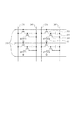
図6は、本発明の一実施形態としての電界効果型トランジスタのチャネル層を成膜するために用いた成膜システムの概略を示す図である。
図6に示すように、本実施の形態の成膜システムは、真空排気能力を制御するゲートバルブ57と、それぞれの気体のシステムへのガス流入量を制御するための個別のマスフローコントローラ56とを有する。また、真空イオンゲージ計54と、基板ホルダー55と、基板51と、ターボ分子ポンプ53と、成膜室58と、スパッタリングターゲット付きスパッタリングガン52とを有する。
53は、成膜室58を1×10⁻⁵Pa(背圧)に達するまで排気するターボ分子真空ポンプである。
55は、基板の位置をx、y面内及び垂直なz方向に調節することができる基板ホルダーである。
52は、スパッタリングガンであり、上に酸化物ターゲット52(ターゲット)を有する。これらの他に、成膜の間に起きる過熱によるスパッタリングガンへの悪影響を防ぐ冷却水供給がある。
59は、スパッタリングターゲットのためのRF電源及びマッチングネットワークである。
FIG. 6 is a diagram showing an outline of a film forming system used for forming a channel layer of a field effect transistor as one embodiment of the present invention.
As shown in FIG. 6, the film forming system of the present embodiment includes a gate valve 57 that controls the evacuation capability, and an individual mass flow controller 56 that controls the amount of gas flowing into each system. Have. Moreover, it has a
53 is a turbo molecular vacuum pump that evacuates the film forming chamber 58 until it reaches 1 × 10 −5 Pa (back pressure).
A
59 is an RF power source and matching network for the sputtering target.
ガス導入配管には、アルゴンガスの導入配管と希釈酸素ガス(Ar:O2=95:5)の導入配管とのそれぞれに一つずつマスフローコントローラ(MFC)56がある。
As the gas introduction pipe, there is one mass flow controller (MFC) 56 for each of the argon gas introduction pipe and the diluted oxygen gas (Ar:
したがって、MFC56でアルゴンと希釈酸素ガスの流入量を制御し、ゲートバルブを用いて圧力を制御することで、成膜室内に所定の雰囲気(全圧と酸素分圧)に調整できる。 Therefore, by controlling the inflow amounts of argon and diluted oxygen gas by the MFC 56 and controlling the pressure using the gate valve, the film formation chamber can be adjusted to a predetermined atmosphere (total pressure and oxygen partial pressure).
本実施例では、まず、2インチIn2O3セラミックターゲット、2インチZnOセラミックターゲットの同時スパッタリングによって、第1のアモルファス酸化物半導体層(Zn−In−O膜)11(a)を成膜する。次いで、0.3〜1Paの範囲内で真空雰囲気を維持した状態で、第2のアモルファス酸化物半導体層(Zn−In−Ge−O膜)11(b)を成膜する。このとき、ターゲットとしては、2インチIn2O3セラミックターゲット、2インチGeO2セラミックターゲット、2インチZnOセラミックターゲットを用いて同時スパッタリングによって成膜する。 In this embodiment, first, a first amorphous oxide semiconductor layer (Zn—In—O film) 11 (a) is formed by simultaneous sputtering of a 2 inch In 2 O 3 ceramic target and a 2 inch ZnO ceramic target. . Next, a second amorphous oxide semiconductor layer (Zn—In—Ge—O film) 11 (b) is formed in a state where a vacuum atmosphere is maintained within a range of 0.3 to 1 Pa. At this time, as a target, a 2-inch In 2 O 3 ceramic target, a 2-inch GeO 2 ceramic target, and a 2-inch ZnO ceramic target are used for film formation by simultaneous sputtering.
第1のアモルファス酸化物半導体層の成膜中は、In2O3ターゲットには35W、ZnOターゲットには46Wの一定値(不可避的な振れ幅は許容する、以下同様)になるようにRF電源を維持する。また、第2のアモルファス酸化物半導体層の成膜中は、In2O3ターゲットには印加電力がそれぞれ、35W、GeO2ターゲットには30W、ZnOターゲットには45Wの一定値になるようにRF電源を維持する。 During the formation of the first amorphous oxide semiconductor layer, the RF power source is set to a constant value of 35 W for the In 2 O 3 target and 46 W for the ZnO target (the inevitable swing width is allowed, and so on). To maintain. Further, during the formation of the second amorphous oxide semiconductor layer, RF is applied so that the applied power is a constant value of 35 W for the In 2 O 3 target, 30 W for the GeO 2 target, and 45 W for the ZnO target, respectively. Maintain power.
成膜時の全ガス圧及びArとO2との流量比は、それぞれ0.4Pa及び69:1である。成膜速度は、第2および第1のアモルファス酸化物半導体層についてそれぞれおよそ11nm/分、9nm/分であり、それぞれの層を約15nmの厚さで形成する。さらに、成膜時基板温度は室温(〜25℃)に保持する。 The total gas pressure at the time of film formation and the flow ratio of Ar and O 2 are 0.4 Pa and 69: 1, respectively. The deposition rates are approximately 11 nm / min and 9 nm / min for the second and first amorphous oxide semiconductor layers, respectively, and each layer is formed with a thickness of approximately 15 nm. Further, the substrate temperature during film formation is kept at room temperature (˜25 ° C.).
次に、フォトリソグラフィーパターン形成法とリフトオフ法とによって、ドレイン電極24及びソース電極23をパターン形成した。ソース及びドレインは、それぞれ100nm及び5nmの厚さを有するAuとTiとの層状構造体である。
Next, the
さらに、本実施例ではチャネルの幅および長さはそれぞれ150μmおよび10μmとし、異なるチャネル組成よりなる素子を作製する。 Further, in this embodiment, the channel width and length are 150 μm and 10 μm, respectively, and devices having different channel compositions are manufactured.
(TFT素子の特性の評価)
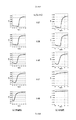
上記手順によって作成したTFTの電圧−電流特性を評価する。図2(a)は、室温で測定した、本実施例のZn−In−Ge−O/Zn−In−O(第2のアモルファス酸化物半導体層/第1のアモルファス酸化物半導体層)積層チャネルからなるTFTのトランスファ特性を示すグラフである。ここで、第1のアモルファス酸化物層25(a)におけるIn/(In+Zn)が0.27〜0.65の範囲内で異なる5つのグラフが示してあり、第2のアモルファス酸化物層25(b)の組成比はIn:Zn:Ge〜42:45:13を有する。第1のアモルファス酸化物層の幅広いIn組成比において、TFTと動作が確認できる。
(Evaluation of TFT element characteristics)
The voltage-current characteristics of the TFT prepared by the above procedure are evaluated. FIG. 2A shows a Zn—In—Ge—O / Zn—In—O (second amorphous oxide semiconductor layer / first amorphous oxide semiconductor layer) stacked channel of this example measured at room temperature. It is a graph which shows the transfer characteristic of TFT which consists of. Here, five different graphs showing In / (In + Zn) in the range of 0.27 to 0.65 in the first amorphous oxide layer 25 (a) are shown, and the second amorphous oxide layer 25 ( The composition ratio of b) has In: Zn: Ge to 42:45:13. TFT and operation can be confirmed in a wide In composition ratio of the first amorphous oxide layer.
比較例として、上記第1のアモルファス酸化物層と同じ組成比を有する、Zn−In−O膜一層のチャネル層からなるTFTの電流−電圧特性を図2(b)に示す。Inの組成比が高くなると、スイッチ電圧が下がり、TFTとして作動しなくなっている。 As a comparative example, FIG. 2B shows the current-voltage characteristics of a TFT composed of a channel layer of one Zn—In—O film having the same composition ratio as the first amorphous oxide layer. When the In composition ratio increases, the switch voltage decreases and the TFT does not operate.
図3は、本実施例1の積層チャンネルTFTに関して、第1のアモルファス酸化物半導体層におけるIn/(In+Zn)の関数として、TFTのオン・オフ電流比を示すグラフである。比較のため、Zn−In−O一層(単層)のチャネル層からなるTFTのオン・オフ電流比も合わせて示している。ここでは、ゲート電圧が20Vおよび−20Vの間で、オンおよびオフ電流値を測定している。一層では動作しなかった、In組成比の高い領域でも、高いオン・オフ比が得られていることが分かる。 FIG. 3 is a graph showing the on / off current ratio of the TFT as a function of In / (In + Zn) in the first amorphous oxide semiconductor layer for the stacked channel TFT of Example 1. For comparison, the on / off current ratio of a TFT composed of a channel layer of one Zn—In—O layer (single layer) is also shown. Here, the on and off current values are measured when the gate voltage is between 20V and −20V. It can be seen that a high on / off ratio was obtained even in a region with a high In composition ratio, which did not operate in a single layer.
図2において、第1のアモルファス酸化物層のIn/(In+Zn)が0.27のとき、オン電圧(スイッチング電圧ともいう)Voが正のノーマリーオフ型TFTが得られる。今回のVoのIn/(In+Zn)値依存性の関係より、本実施例では第1のアモルファス酸化物層のIn/(In+Zn)がおよそ0.3以下でVoが正のTFTが実現可能と見積もられる。 In FIG. 2, when In / (In + Zn) of the first amorphous oxide layer is 0.27, a normally-off TFT having a positive on-voltage (also referred to as switching voltage) Vo is obtained. From the relationship of the dependence of Vo on the In / (In + Zn) value, it is estimated that in this embodiment, a TFT with a positive Vo can be realized when In / (In + Zn) of the first amorphous oxide layer is about 0.3 or less. It is.
また、図3からみて取れるように、第1のアモルファス酸化物層のIn/(In+Zn)が0.55以下で、オンオフ比が109以上の電界効果型トランジスタであるTFTが得られている。 Further, as can be seen from FIG. 3, a TFT which is a field effect transistor having In / (In + Zn) of the first amorphous oxide layer of 0.55 or less and an on / off ratio of 10 9 or more is obtained.
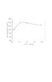
図4は、第1のアモルファス酸化物半導体層におけるIn/(In+Zn)の関数としての電界効果移動度μ(cm2/Vsec)の例を示すグラフである。
In組成比の変化に大きく関わらず、15〜25cm2/Vsecの移動度を実現していることが確認できた。特に、第1のアモルファス酸化物層のIn/(In+Zn)が0.35以上で電界効果移動度μが20cm2/Vsec以上のTFTが得られている。更に、これらを空気中250度で1時間アニールすることにより、第1のアモルファス酸化物層のIn/(In+Zn)が0.65以上においてμが100cm2/Vsec以上のTFTが得られる。
即ち、Zn−In−Oからなる第1のアモルファス酸化物半導体層と、Zn−In−Ge−Oという新しいアモルファス酸化物半導体からなる第2のアモルファス酸化物半導体層からなる、積層チャネルを用いることで、優れたトランジスタ特性を実現することができる。
FIG. 4 is a graph showing an example of the field effect mobility μ (cm 2 / Vsec) as a function of In / (In + Zn) in the first amorphous oxide semiconductor layer.
It was confirmed that the mobility of 15 to 25 cm 2 / Vsec was realized regardless of the change in the In composition ratio. In particular, TFTs having In / (In + Zn) of the first amorphous oxide layer of 0.35 or more and a field effect mobility μ of 20 cm 2 / Vsec or more are obtained. Furthermore, by annealing these at 250 ° C. for 1 hour in the air, a TFT having μ of 100 cm 2 / Vsec or more when In / (In + Zn) of the first amorphous oxide layer is 0.65 or more can be obtained.
That is, a stacked channel including a first amorphous oxide semiconductor layer made of Zn—In—O and a second amorphous oxide semiconductor layer made of a new amorphous oxide semiconductor called Zn—In—Ge—O is used. Thus, excellent transistor characteristics can be realized.
これは、移動度が大きい一方で、組成依存性の影響が大きいZn−In−O系TFTに比べて、大きなオン・オフ電流比を示す組成マージンを広げ、優れたTFT特性を実現することができることを示している。 Compared to Zn-In-O-based TFTs, which have a high mobility but a large composition dependency, this can widen the composition margin showing a large on / off current ratio and realize excellent TFT characteristics. It shows what you can do.
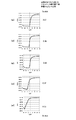
また図5は、第1のアモルファス酸化物半導体層におけるIn/(In+Zn)に対するサブスレッシュホルドスウィング値(S値)(V/dec)である。図5において第1のアモルファス酸化物半導体層におけるIn/(In+Zn)が0.35以下で、S値が1以下のTFTが実現している。この結果から、本実施例においては第1のアモルファス酸化物層のIn/(In+Zn)が0.3以下でS値が1以下のTFTが実現可能と見積もられる。 FIG. 5 is a subthreshold swing value (S value) (V / dec) with respect to In / (In + Zn) in the first amorphous oxide semiconductor layer. In FIG. 5, a TFT having In / (In + Zn) in the first amorphous oxide semiconductor layer of 0.35 or less and an S value of 1 or less is realized. From this result, in this example, it is estimated that a TFT having an In / (In + Zn) of 0.3 or less and an S value of 1 or less in the first amorphous oxide layer can be realized.
TFT性能が良好なことから、OLEDの動作回路中に本発明のIn−Ge−Oチャネル層薄膜トランジスタを使用すると有望である。 Since the TFT performance is good, it is promising to use the In-Ge-O channel layer thin film transistor of the present invention in the operation circuit of the OLED.
以上、実施例1について、図2(a)のTFTのトランスファ特性では、第1のアモルファス酸化物層のIn/(In+Zn)が0.27のとき、オン電圧(スイッチング電圧ともいう)Voが正のノーマリーオフ型TFTが得られている。このため、今回のVoのIn/(In+Zn)値依存性の関係より、第1のアモルファス酸化物層のIn/(In+Zn)がおよそ0.3以下でVoが正のTFTが実現可能と見積もられる。すなわち、ノーマリオフTFTを実現するという観点から、第1のアモルファス酸化物半導体層の組成比In/(In+Zn)が0.3以下であることが好ましい。また、第1のアモルファス酸化物半導体層のIn/(In+Zn)が0.57以下でオフ電流が10−12以下のTFTが得られている。すなわち、オフ電流が小さいTFTを実現するという観点から、第1のアモルファス酸化物半導体層の組成比In/(In+Zn)が0.57以下であることが好ましい。さらに、図3では、実施例1の第1のアモルファス酸化物層のIn/(In+Zn)が0.6以下で、オンオフ比が109以上の電界効果型トランジスタであるTFTが得られている。すなわち、オンオフ比の大きいTFTを実現するという観点から、実施例1の第1のアモルファス酸化物半導体層の組成比In/(In+Zn)はおよそ0.6以下、より好ましくは0.55以下であることが好ましい。 As described above, in Example 1, in the TFT transfer characteristics of FIG. 2A, when In / (In + Zn) of the first amorphous oxide layer is 0.27, the on-voltage (also referred to as switching voltage) Vo is positive. The normally-off type TFT is obtained. For this reason, it is estimated that a TFT with a positive Vo can be realized when the In / (In + Zn) of the first amorphous oxide layer is about 0.3 or less from the relationship of the dependency of Vo on the In / (In + Zn) value. . That is, from the viewpoint of realizing a normally-off TFT, the composition ratio In / (In + Zn) of the first amorphous oxide semiconductor layer is preferably 0.3 or less. In addition, a TFT with In / (In + Zn) of the first amorphous oxide semiconductor layer of 0.57 or less and an off current of 10 −12 or less is obtained. That is, from the viewpoint of realizing a TFT with a low off-state current, the composition ratio In / (In + Zn) of the first amorphous oxide semiconductor layer is preferably 0.57 or less. Further, in FIG. 3, the first In / amorphous oxide layer (In + Zn) is 0.6 or less in Example 1, TFT is obtained on-off ratio of 10 9 or more of the field effect transistor. That is, from the viewpoint of realizing a TFT with a large on / off ratio, the composition ratio In / (In + Zn) of the first amorphous oxide semiconductor layer of Example 1 is about 0.6 or less, more preferably 0.55 or less. It is preferable.
また、図4より、実施例1では、In組成比の変化に大きく関わらず、15〜25cm2/Vsecの移動度を実現していることが確認できる。特に、第1のアモルファス酸化物層のIn/(In+Zn)が0.35以上で電界効果移動度μが20cm2/Vsec以上のTFTが得られている。すなわち、この結果と電界効果移動度の大きいTFTを実現するという観点から、実施例1の第1のアモルファス酸化物半導体層の組成比In/(In+Zn)は0.3以上であることが好ましい。 Moreover, it can be confirmed from FIG. 4 that the mobility of 15 to 25 cm 2 / Vsec is realized in Example 1 regardless of the change in the In composition ratio. In particular, TFTs having In / (In + Zn) of the first amorphous oxide layer of 0.35 or more and a field effect mobility μ of 20 cm 2 / Vsec or more are obtained. That is, from the viewpoint of realizing this result and a TFT having a large field effect mobility, the composition ratio In / (In + Zn) of the first amorphous oxide semiconductor layer of Example 1 is preferably 0.3 or more.
また図5には、第1のアモルファス酸化物半導体層におけるIn/(In+Zn)に対するサブスレッシュホルドスウィング値(S値)(V/dec)を示している。第1のアモルファス酸化物半導体層におけるIn/(In+Zn)が0.35以下で、S値が1以下のTFTが得られる。この結果から、実施例1においては第1のアモルファス酸化物半導体層のIn/(In+Zn)が0.4以下でS値が1以下のTFTが実現可能と見積もられる。すなわち、S値の小さいTFTを実現するという観点から、実施例1の第1のアモルファス酸化物半導体層の組成比In/(In+Zn)が0.4以下であることが好ましい。 FIG. 5 shows a subthreshold swing value (S value) (V / dec) with respect to In / (In + Zn) in the first amorphous oxide semiconductor layer. A TFT having In / (In + Zn) in the first amorphous oxide semiconductor layer of 0.35 or less and an S value of 1 or less is obtained. From this result, in Example 1, it is estimated that a TFT having In / (In + Zn) of 0.4 or less and an S value of 1 or less in the first amorphous oxide semiconductor layer can be realized. That is, from the viewpoint of realizing a TFT having a small S value, the composition ratio In / (In + Zn) of the first amorphous oxide semiconductor layer of Example 1 is preferably 0.4 or less.
(実施例2)
実施例2では、図1(a)に示すトップゲート型電解効果型トランジスタを用いて実施例1と同様の評価を行う。具体的には、チャネル層は、第1のアモルファス酸化物層11(a)としてZn−In−Oを用い、第2のアモルファス酸化物層11(b)はZn−In−Ge−Oを用いる。こうして、図1(a)に示すトップゲート型電解効果型トランジスタを作製して実施例1と同様に評価を行う。その結果実施例1と同様に本発明の薄膜トランジスタの効果を確認することができる。
(Example 2)
In Example 2, the same evaluation as in Example 1 is performed using the top gate type field effect transistor shown in FIG. Specifically, the channel layer uses Zn—In—O as the first amorphous oxide layer 11 (a), and the second amorphous oxide layer 11 (b) uses Zn—In—Ge—O. . Thus, the top gate type field effect transistor shown in FIG. 1A is manufactured and evaluated in the same manner as in Example 1. As a result, the effect of the thin film transistor of the present invention can be confirmed as in Example 1.
(実施例3)
実施例3では図1(b)に示すボトムゲート型電解効果型トランジスタを用いて実施例1と同様の評価を行った。具体的にはチャネル層として、第1のアモルファス酸化物層11(a)としてZn−In−Oを用い、第2のアモルファス酸化物層11(b)としてZn−In−Ge−Oを用いる。こうして、図1(b)に示すゲート電極15の上にゲート絶縁層12と半導体チャネル層11を有するボトムゲート型電解効果型トランジスタを作製して実施例1と同様に評価を行う。その結果実施例1と同様に本発明の薄膜トランジスタの効果を確認することができる。
(Example 3)
In Example 3, the same evaluation as in Example 1 was performed using the bottom gate type field effect transistor shown in FIG. Specifically, as the channel layer, Zn—In—O is used as the first amorphous oxide layer 11 (a), and Zn—In—Ge—O is used as the second amorphous oxide layer 11 (b). In this way, a bottom gate field effect transistor having the
(実施例4)
実施例4では、実施例1における第1のアモルファス酸化物半導体層の電気物性について示す。In/(In+Zn)が0.45のZn−In−O膜のホール移動度を評価した結果を表1(a)に示す。薄膜の作製条件は、実施例1の第1のアモルファス酸化物半導体層の成膜条件に準じている。膜厚は300nmであり、250℃空気中で1時間アニール処理を施した。
薄膜は、X線回折よりアモルファスであることが確認される。
Example 4
In Example 4, electrical properties of the first amorphous oxide semiconductor layer in Example 1 will be described. Table 1 (a) shows the results of evaluating the hole mobility of the Zn—In—O film having In / (In + Zn) of 0.45. The conditions for forming the thin film are in accordance with the conditions for forming the first amorphous oxide semiconductor layer of Example 1. The film thickness was 300 nm, and annealing treatment was performed in air at 250 ° C. for 1 hour.
The thin film is confirmed to be amorphous by X-ray diffraction.
次に、第2のアモルファス酸化物半導体層の電気物性について説明する。In:Zn:Geが42:45:13のZn−In−Ge−O膜のホール移動度を評価した結果を表1(b)に示す。薄膜の作製条件は、実施例1の第1のアモルファス酸化物半導体層の成膜条件に準じている。膜厚は300nm程度であり、250℃空気中で、1時間アニール処理を施す。
薄膜は、X線回折よりアモルファスであることが確認される。これらの結果より、Zn−In−O膜はZn−In−Ge−O膜よりも大きな移動度特性を示すことがわかる。実施例1のデバイス構成においては、第1のアモルファス酸化物半導体層(Zn−In−O)の材料の電子移動度が第2のアモルファス酸化物半導体層(Zn−In−Ge−O)の材料の電子移動度より大きいことがわかる。実施例1では、ゲート絶縁層に接する側(第1のアモルファス酸化物半導体層)に大きな電子移動度の材料を適用することで、大きな電界効果移動度を示すTFTを実現できると考えられる。
Next, electrical properties of the second amorphous oxide semiconductor layer will be described. Table 1 (b) shows the results of evaluating the hole mobility of the Zn—In—Ge—O film having In: Zn: Ge of 42:45:13. The conditions for forming the thin film are in accordance with the conditions for forming the first amorphous oxide semiconductor layer of Example 1. The film thickness is about 300 nm, and annealing treatment is performed in air at 250 ° C. for 1 hour.
The thin film is confirmed to be amorphous by X-ray diffraction. From these results, it can be seen that the Zn—In—O film exhibits higher mobility characteristics than the Zn—In—Ge—O film. In the device configuration of Example 1, the electron mobility of the material of the first amorphous oxide semiconductor layer (Zn—In—O) is the material of the second amorphous oxide semiconductor layer (Zn—In—Ge—O). It can be seen that the electron mobility is larger than. In Example 1, it is considered that a TFT having a large field effect mobility can be realized by applying a material having a large electron mobility to the side in contact with the gate insulating layer (first amorphous oxide semiconductor layer).
また、本実施例の結果は、Zn−In−Ge−O膜がZn−In−O膜よりも小さなキャリア濃度となることを示している。これらの結果より、実施例1のデバイス構成において、第1のアモルファス酸化物半導体層の材料のキャリア濃度が第2のアモルファス酸化物半導体層の材料のキャリア濃度より大きいことがわかる。ゲート絶縁層に接する側(第1のアモルファス酸化物半導体層)に比較的大きなキャリア濃度を有した材料を適用しているにもかかわらず、第2のアモルファス酸化物半導体層にキャリア濃度の低い膜を用いることで、大きなオンオフ比を示すTFTを実現できたと考えられる。 In addition, the result of this example shows that the Zn—In—Ge—O film has a lower carrier concentration than the Zn—In—O film. From these results, it can be seen that in the device configuration of Example 1, the carrier concentration of the material of the first amorphous oxide semiconductor layer is higher than the carrier concentration of the material of the second amorphous oxide semiconductor layer. A film having a low carrier concentration is applied to the second amorphous oxide semiconductor layer even though a material having a relatively large carrier concentration is applied to the side in contact with the gate insulating layer (first amorphous oxide semiconductor layer). It is considered that a TFT having a large on / off ratio could be realized by using.

(実施例5)
実施例5では、実施例1と同様に作製した薄膜トランジスタに対して、引き続き、空気中において250℃で1時間アニールを行い、実施例1と同様の評価を行った。図11は、室温で測定した、本実施例のTFTの伝達特性を示すグラフである。第1のアモルファス酸化物半導体層11(a)In/(In+Zn)が0.27〜0.65の範囲内で異なる5つのグラフが示してあり、第2のアモルファス酸化物半導体層11(b)の組成比はIn:Zn:Ge〜42:45:13を有する。実施例1と同様に、第1のアモルファス酸化物半導体層のIn/(In+Zn)値が0.27〜0.65に対してTFTの動作を確認できた。
(Example 5)
In Example 5, the thin film transistor manufactured in the same manner as in Example 1 was subsequently annealed in air at 250 ° C. for 1 hour, and the same evaluation as in Example 1 was performed. FIG. 11 is a graph showing the transfer characteristics of the TFT of this example measured at room temperature. The first amorphous oxide semiconductor layer 11 (a) Five graphs in which In / (In + Zn) is different within the range of 0.27 to 0.65 are shown, and the second amorphous oxide semiconductor layer 11 (b) The composition ratio of In: Zn: Ge is 42:45:13. As in Example 1, the operation of the TFT was confirmed when the In / (In + Zn) value of the first amorphous oxide semiconductor layer was 0.27 to 0.65.
さらに、図12は、本実施例の第1のアモルファス酸化物半導体層におけるIn/(In+Zn)の関数としての電界効果移動度μ(cm2/Vsec)の例を示すグラフである。In組成比の大きい素子において、高い電界効果移動度が得られた。特に、第1のアモルファス酸化物半導体層におけるIn/(In+Zn)値が0.65の素子で、150cm2/Vsec以上のTFTが得られた。更に、第1のアモルファス酸化物半導体層におけるIn/(In+Zn)がおよそ0.57と0.65のTFTについて、その伝達特性:図13(a)、(c)と電界効果移動度μ(cm2/Vsec):図13(b)、(d)、を示す。 Further, FIG. 12 is a graph showing an example of the field effect mobility μ (cm 2 / Vsec) as a function of In / (In + Zn) in the first amorphous oxide semiconductor layer of this example. In a device having a large In composition ratio, high field effect mobility was obtained. In particular, a TFT having an In / (In + Zn) value of 0.65 in the first amorphous oxide semiconductor layer was obtained with a TFT of 150 cm 2 / Vsec or more. Furthermore, transfer characteristics of TFTs having In / (In + Zn) of about 0.57 and 0.65 in the first amorphous oxide semiconductor layer: FIGS. 13A and 13C and field effect mobility μ (cm 2 / Vsec): FIGS. 13B and 13D are shown.
これらのIn/(In+Zn)組成比(In組成の高い組成領域)において単層チャネルのTFTを作製すると、マイナスのゲート電圧を印加しても、十分なオフ状態を得ることすることが困難である。一方で、本実施例の構成では、負のゲート電圧を印加することで、Idを10−10A以下にまで減少させること(オフすること)が可能である。 When a single-layer channel TFT is manufactured with these In / (In + Zn) composition ratio (composition region with a high In composition), it is difficult to obtain a sufficient off state even when a negative gate voltage is applied. . On the other hand, in the configuration of the present embodiment, it is possible to reduce (turn off) Id to 10 −10 A or less by applying a negative gate voltage.
さらに、図13(b)、(d)に示すように、電界効果移動度は100を超える値が得られた。このように、本実施例では高い電流伝達が可能になっており、高移動度トランジスタとしての使用可能性が広い。 Further, as shown in FIGS. 13B and 13D, a field effect mobility of more than 100 was obtained. Thus, in this embodiment, high current transmission is possible, and the possibility of use as a high mobility transistor is wide.
すなわち、本実施例の積層チャンネルを適用したTFTにおいては、第1のアモルファス酸化物半導体層にIn含有量が大きい酸化物半導体を適用することができる。これにより、単層チャネル構造では困難なレベルの大きな電界効果移動度を有したTFTを実現できる。 That is, in the TFT to which the stacked channel of this embodiment is applied, an oxide semiconductor having a large In content can be applied to the first amorphous oxide semiconductor layer. Thereby, it is possible to realize a TFT having a large field-effect mobility that is difficult to achieve with a single-layer channel structure.
また、図10には、ゲート電圧-4Vから20VでのId−Vd特性を示す。典型的なトランジスタ特性としてピンチオフ特性(Vdの増加とともにIdの飽和する現象)が認められる。 FIG. 10 shows the Id-Vd characteristics from a gate voltage of −4V to 20V. A pinch-off characteristic (a phenomenon in which Id saturates as Vd increases) is recognized as a typical transistor characteristic.
(実施例6)
実施例6では、図1(a)に示すトップゲート型電界効果型トランジスタの例を示す。具体的には、チャネル層として、第1のアモルファス酸化物半導体層11(a)はZn−In−Oからなり、第2のアモルファス酸化物半導体層11(b)はZn−In−Ge−Oからなる。第1のアモルファス酸化物半導体層における組成比は、In:Zn〜40:60であり、第2のアモルファス酸化物半導体層における組成比は、In:Zn:Ge〜43:46:11である。
(Example 6)
Example 6 shows an example of the top gate type field effect transistor shown in FIG. Specifically, as the channel layer, the first amorphous oxide semiconductor layer 11 (a) is made of Zn—In—O, and the second amorphous oxide semiconductor layer 11 (b) is made of Zn—In—Ge—O. Consists of. The composition ratio in the first amorphous oxide semiconductor layer is In: Zn to 40:60, and the composition ratio in the second amorphous oxide semiconductor layer is In: Zn: Ge to 43:46:11.
10はガラス基板、13,14はMoからなるソース及びドレイン電極、12はSiOxからなるゲート絶縁膜、15はMoからなるゲート電極である。実施例1と比べて、2つの材料の積層順序が逆である。ゲート絶縁膜に接する側の材料がZn−In−Oであること点に関して、実施例1と共通である。 10 is a glass substrate, 13 and 14 are source and drain electrodes made of Mo, 12 is a gate insulating film made of SiO x , and 15 is a gate electrode made of Mo. Compared to Example 1, the stacking order of the two materials is reversed. In common with Example 1, the material on the side in contact with the gate insulating film is Zn—In—O.
このような積層チャネル構造を適用することで、実施例1同様に、移動度が大きく、組成比に対する特性変動の小さい薄膜トランジスタとすることができる。 By applying such a stacked channel structure, a thin film transistor having high mobility and small characteristic variation with respect to the composition ratio can be obtained as in the first embodiment.
(実施例7)
実施例7では図1(b)に示すボトムゲート型電界効果型トランジスタの例である。具体的にはチャネル層として、第1のアモルファス酸化物半導体層11(a)はZn−In−Oからなり、第2のアモルファス酸化物半導体層11(b)はZn−In−Si−Oからなる。第1のアモルファス酸化物半導体層における組成比は、In:Zn〜38:62であり、第2のアモルファス酸化物半導体層における組成比は、In:Zn:Si〜44:47:9である。10はガラス基板、13,14はAu/Tiからなるソース及びドレイン電極、12はSiOxからなるゲート絶縁膜、15はMoからなるゲート電極である。
(Example 7)
Example 7 is an example of a bottom gate type field effect transistor shown in FIG. Specifically, as the channel layer, the first amorphous oxide semiconductor layer 11 (a) is made of Zn—In—O, and the second amorphous oxide semiconductor layer 11 (b) is made of Zn—In—Si—O. Become. The composition ratio in the first amorphous oxide semiconductor layer is In: Zn to 38:62, and the composition ratio in the second amorphous oxide semiconductor layer is In: Zn: Si to 44: 47: 9. 10 is a glass substrate, 13 and 14 are source / drain electrodes made of Au / Ti, 12 is a gate insulating film made of SiO x , and 15 is a gate electrode made of Mo.
このような積層チャネル構造を適用することで、実施例1のボトムゲート型の構成と同様に、移動度が大きく、組成比に対する特性変動の小さい薄膜トランジスタとすることができる。 By applying such a stacked channel structure, a thin film transistor having a high mobility and a small characteristic variation with respect to the composition ratio can be obtained as in the bottom-gate structure of Example 1.
(実施例8)
本実施例8は、本発明の積層チャネルTFTの駆動安定性を評価した例である。
本実施例8では、実施例5の構成の素子(第1のアモルファス酸化物半導体層の組成はZn:In〜36:64、第2のアモルファス酸化物半導体層の組成はIn:Zn:Ge〜42:45:13)に対して、一定期間の電圧印加(ストレス)を行い、その前後でのTFT特性(伝達特性)の差異を比較した。電圧ストレスにおいては、直流電圧を用い、ゲート電圧(Vg=12V)と、ソースドレイン電圧(Vd=6V)を同時印加した。電圧印加時間は800secである。
ストレス前後の伝達特性から抽出したTFT特性パラメータ(Vo,S,Vt,μ)の差異を表2(a)に示す。表2(b)には、比較例として、上記第1のアモルファス酸化物半導体層と同じ組成比を有する、Zn−In−O膜単層のチャネル層からなる素子のストレス耐性測定結果も共に示している。比較例では、スイッチング電圧(Vo)のシフトが0.64Vであるのに対して、本実施例ではVoのシフトが0.33Vと大きく軽減されている。これより、本実施例のTFTでは、駆動に対して高い安定性を有することがわかる。
(Example 8)
Example 8 is an example in which the driving stability of the laminated channel TFT of the present invention was evaluated.
In Example 8, the element having the configuration of Example 5 (the composition of the first amorphous oxide semiconductor layer is Zn: In to 36:64, the composition of the second amorphous oxide semiconductor layer is In: Zn: Ge) 42:45:13), voltage application (stress) was applied for a certain period, and the difference in TFT characteristics (transfer characteristics) before and after that was compared. In the voltage stress, a DC voltage was used, and a gate voltage (Vg = 12V) and a source / drain voltage (Vd = 6V) were applied simultaneously. The voltage application time is 800 sec.
Differences in TFT characteristic parameters (Vo, S, Vt, μ) extracted from the transfer characteristics before and after stress are shown in Table 2 (a). Table 2 (b) shows, as a comparative example, the stress resistance measurement results of a device composed of a channel layer of a single Zn—In—O film having the same composition ratio as that of the first amorphous oxide semiconductor layer. ing. In the comparative example, the shift of the switching voltage (Vo) is 0.64V, whereas in this embodiment, the shift of Vo is greatly reduced to 0.33V. From this, it can be seen that the TFT of this example has high stability with respect to driving.
(実施例9)
実施例9では、図1(c)に示すボトムゲート型電界効果型トランジスタの例を示す。具体的には、チャネル層の第1のアモルファス酸化物半導体層11(a)としてZn−In−O系膜を選択した。また、第2のアモルファス酸化物半導体層11(b)としては第1のアモルファス酸化物半導体層11(a)と異なる組成を有するZn−In−O系半導体膜を選択した。第1のアモルファス酸化物半導体層における組成比は、In/(In+Zn)0.57であり、第2のアモルファス酸化物半導体層における組成比は、In/(In+Zn)0.48である。
基板10はn+型Si基板、ソース及びドレイン電極13と14はそれぞれ100nm及び5nmの厚さを有するAuとTiとの層状構造体からなり、ゲート絶縁膜12はSiOxからなる。
Example 9
Example 9 shows an example of a bottom gate type field effect transistor shown in FIG. Specifically, a Zn—In—O-based film was selected as the first amorphous oxide semiconductor layer 11 (a) of the channel layer. As the second amorphous oxide semiconductor layer 11 (b), a Zn—In—O based semiconductor film having a composition different from that of the first amorphous oxide semiconductor layer 11 (a) was selected. The composition ratio in the first amorphous oxide semiconductor layer is In / (In + Zn) 0.57, and the composition ratio in the second amorphous oxide semiconductor layer is In / (In + Zn) 0.48.
The
図14は、室温で測定した、本実施例のTFTの伝達特性を示すグラフである。前述の比較例においては、チャネル層のIn/(In+Zn)値が0.57のとき、図2(b4)に示したようにTFT作動していない。一方、本実施例のTFTでは、図14に示すように動作が確認できる。 FIG. 14 is a graph showing the transfer characteristics of the TFT of this example measured at room temperature. In the comparative example described above, when the In / (In + Zn) value of the channel layer is 0.57, the TFT does not operate as shown in FIG. 2 (b4). On the other hand, the operation of the TFT of this example can be confirmed as shown in FIG.
本実施例と比較例を比べ、本実施例の積層チャンネル構成は単層チャネル構成(比較例)とくらべて、より広い組成比In/(In+Zn)比に対して、TFT動作が可能であることが確認される。 Compared with the present example and the comparative example, the stacked channel configuration of the present example is capable of TFT operation with a wider composition ratio In / (In + Zn) ratio than the single layer channel configuration (comparative example). Is confirmed.
このような積層チャネル構造を適用することで、実施例1同様に、移動度が大きく、組成比に対する特性変動の小さい薄膜トランジスタとすることができる。 By applying such a stacked channel structure, a thin film transistor having high mobility and small characteristic variation with respect to the composition ratio can be obtained as in the first embodiment.
(比較例)
比較例として、実施例1の第一のアモルファス酸化物層と同じ組成比を有する、Zn−In−O膜一層のチャネル層からなるTFTの電流−電圧特性を図2(b)に示した。Inの組成比が高くなると、スイッチ電圧が下がり、TFTとして作動しなくなっている。
(Comparative example)
As a comparative example, FIG. 2B shows the current-voltage characteristics of a TFT having the same composition ratio as that of the first amorphous oxide layer of Example 1 and composed of a channel layer of one Zn—In—O film. When the In composition ratio increases, the switch voltage decreases and the TFT does not operate.
本比較例においては、In/(In+Zn)が0.27と0.36の素子ではスイッチング動作を示しているものの、Inの組成比が高くなると(In/(In+Zn)が0.45)ともに、スイッチング電圧Voが下がる。さらにはIn/(In+Zn)が0.57および0.65では、TFTとして作動しなくなっている。 In this comparative example, the elements with In / (In + Zn) of 0.27 and 0.36 show a switching operation, but when the In composition ratio increases (In / (In + Zn) is 0.45), The switching voltage Vo decreases. Further, when In / (In + Zn) is 0.57 and 0.65, the TFT does not operate.
図2で実施例1と比較例を比べると、本実施例の積層チャンネル構成は単層チャネル構成(比較例)とくらべて、より広い組成比In/(In+Zn)比に対して、TFT動作が可能であることがわかる。 Compared with Example 1 and the comparative example in FIG. 2, the stacked channel configuration of this example has a TFT operation for a wider composition ratio In / (In + Zn) ratio than the single layer channel configuration (comparative example). It turns out that it is possible.
さらに、図3で、実施例1と比較例のオン・オフ比を比べると、比較例(単層Zn−In−Oチャネル)では、In組成比の大きい組成で著しくオン・オフ比が減少しているが、本実施例1の積層チャンネルTFTでは広い組成範囲にわたり高いオン・オフ比が得られていることが分かる。すなわち、本実施例においては、組成変動に対するTFT特性の変動が小さいといえる。 Further, when the on / off ratios of Example 1 and the comparative example are compared in FIG. 3, in the comparative example (single layer Zn—In—O channel), the on / off ratio is remarkably reduced at a composition having a large In composition ratio. However, it can be seen that the laminated channel TFT of Example 1 has a high on / off ratio over a wide composition range. That is, in this example, it can be said that the variation of the TFT characteristics with respect to the composition variation is small.
即ち、Zn−In−Oからなる第1のアモルファス酸化物半導体層と、Zn−In−Ge−Oという新しいアモルファス酸化物半導体からなる第2のアモルファス酸化物半導体層からなる、積層チャネルを用いることで、電界効果移動度やオン・オフ電流比などのTFT特性に優れ、且つ、組成比変動に伴う素子特性の変動が小さい優れたトランジスタ特性を実現することができる。 That is, a stacked channel including a first amorphous oxide semiconductor layer made of Zn—In—O and a second amorphous oxide semiconductor layer made of a new amorphous oxide semiconductor called Zn—In—Ge—O is used. Thus, it is possible to realize excellent transistor characteristics that are excellent in TFT characteristics such as field-effect mobility and on / off current ratio and that have small fluctuations in element characteristics due to composition ratio fluctuations.
10 基板
11 チャネル層
11(a) 第1のアモルファス酸化物層
11(b) 第2のアモルファス酸化物層
12 ゲート絶縁層
13 ソース電極
14 ドレイン電極
15 ゲート電極
21 基板
22 ゲート絶縁膜
23 ソース電極
24 ドレイン電極
25 チャネル層
25(a) 第1のアモルファス酸化物層
25(b) 第2のアモルファス酸化物層
DESCRIPTION OF
Claims (11)
積層された半導体層とゲート絶縁層とゲート電極と、を有する電界効果型トランジスタであって、
前記半導体層は、In−Zn−O系酸化物半導体を含有する第1のアモルファス酸化物半導体層と、Ge−In−Zn−O系酸化物半導体を含有する第2のアモルファス酸化物半導体層と、を有し、
前記第1のアモルファス酸化物半導体層が前記ゲート絶縁層に接するように前記第1のアモルファス酸化物半導体層と前記第2のアモルファス酸化物半導体層とが積層されていることを特徴とする電界効果型トランジスタ。 A source electrode and a drain electrode,
A field effect transistor having a stacked semiconductor layer, a gate insulating layer, and a gate electrode,
The semiconductor layer includes: a first amorphous oxide semiconductor layer containing an In—Zn—O-based oxide semiconductor; a second amorphous oxide semiconductor layer containing a Ge—In—Zn—O-based oxide semiconductor; Have
The first amorphous oxide semiconductor layer and the second amorphous oxide semiconductor layer are stacked such that the first amorphous oxide semiconductor layer is in contact with the gate insulating layer. Type transistor.
該電界効果型トランジスタによって駆動される有機EL素子と、を含むことを特徴とする表示装置。 A field effect transistor according to any one of claims 1 to 10,
And an organic EL element driven by the field effect transistor.
Priority Applications (6)
| Application Number | Priority Date | Filing Date | Title |
|---|---|---|---|
| JP2009222514A JP5538797B2 (en) | 2008-12-12 | 2009-09-28 | Field effect transistor and display device |
| EP11009309A EP2423966A1 (en) | 2008-12-12 | 2009-12-03 | Field effect transistor and display apparatus |
| EP09014995A EP2197034B1 (en) | 2008-12-12 | 2009-12-03 | Field effect transistor and display apparatus |
| US12/634,319 US20100148170A1 (en) | 2008-12-12 | 2009-12-09 | Field effect transistor and display apparatus |
| KR1020090121626A KR101215964B1 (en) | 2008-12-12 | 2009-12-09 | Field effect transistor and display apparatus |
| CN2009102585023A CN101752428B (en) | 2008-12-12 | 2009-12-11 | Field effect transistor, manufacturing method of field effect transistors and display device |
Applications Claiming Priority (3)
| Application Number | Priority Date | Filing Date | Title |
|---|---|---|---|
| JP2008317286 | 2008-12-12 | ||
| JP2008317286 | 2008-12-12 | ||
| JP2009222514A JP5538797B2 (en) | 2008-12-12 | 2009-09-28 | Field effect transistor and display device |
Publications (3)
| Publication Number | Publication Date |
|---|---|
| JP2010161339A JP2010161339A (en) | 2010-07-22 |
| JP2010161339A5 JP2010161339A5 (en) | 2012-11-08 |
| JP5538797B2 true JP5538797B2 (en) | 2014-07-02 |
Family
ID=41820261
Family Applications (1)
| Application Number | Title | Priority Date | Filing Date |
|---|---|---|---|
| JP2009222514A Expired - Fee Related JP5538797B2 (en) | 2008-12-12 | 2009-09-28 | Field effect transistor and display device |
Country Status (5)
| Country | Link |
|---|---|
| US (1) | US20100148170A1 (en) |
| EP (2) | EP2423966A1 (en) |
| JP (1) | JP5538797B2 (en) |
| KR (1) | KR101215964B1 (en) |
| CN (1) | CN101752428B (en) |
Families Citing this family (44)
| Publication number | Priority date | Publication date | Assignee | Title |
|---|---|---|---|---|
| KR101648927B1 (en) | 2009-01-16 | 2016-08-17 | 가부시키가이샤 한도오따이 에네루기 켄큐쇼 | Semiconductor device and manufacturing method thereof |
| US8492756B2 (en) * | 2009-01-23 | 2013-07-23 | Semiconductor Energy Laboratory Co., Ltd. | Semiconductor device and method for manufacturing the same |
| TWI476917B (en) * | 2009-04-16 | 2015-03-11 | Semiconductor Energy Lab | Semiconductor device and manufacturing method thereof |
| KR102089200B1 (en) | 2009-11-28 | 2020-03-13 | 가부시키가이샤 한도오따이 에네루기 켄큐쇼 | Semiconductor device and manufacturing method thereof |
| KR102253973B1 (en) * | 2010-01-20 | 2021-05-18 | 가부시키가이샤 한도오따이 에네루기 켄큐쇼 | Display device |
| WO2011111505A1 (en) * | 2010-03-08 | 2011-09-15 | Semiconductor Energy Laboratory Co., Ltd. | Semiconductor device and method for manufacturing semiconductor device |
| EP2589085B1 (en) * | 2010-07-02 | 2019-02-20 | Hewlett-Packard Development Company, L.P. | Thin film transistors |
| US8593858B2 (en) * | 2010-08-31 | 2013-11-26 | Semiconductor Energy Laboratory Co., Ltd. | Driving method of semiconductor device |
| JP5666616B2 (en) * | 2010-10-25 | 2015-02-12 | 株式会社日立製作所 | Manufacturing method of oxide semiconductor device |
| JP2012099661A (en) * | 2010-11-02 | 2012-05-24 | Idemitsu Kosan Co Ltd | Method of manufacturing oxide semiconductor |
| KR101457833B1 (en) * | 2010-12-03 | 2014-11-05 | 가부시키가이샤 한도오따이 에네루기 켄큐쇼 | Semiconductor device |
| JP2012151453A (en) | 2010-12-28 | 2012-08-09 | Semiconductor Energy Lab Co Ltd | Semiconductor device and driving method of the same |
| TWI572009B (en) | 2011-01-14 | 2017-02-21 | 半導體能源研究所股份有限公司 | Semiconductor memory device |
| JP6053098B2 (en) * | 2011-03-28 | 2016-12-27 | 株式会社半導体エネルギー研究所 | Semiconductor device |
| JP2012235104A (en) * | 2011-04-22 | 2012-11-29 | Kobe Steel Ltd | Thin film transistor structure, and thin film transistor and display device including the structure |
| JP2012238763A (en) * | 2011-05-12 | 2012-12-06 | Fujitsu Ltd | Semiconductor device and method of manufacturing semiconductor device |
| US8952377B2 (en) | 2011-07-08 | 2015-02-10 | Semiconductor Energy Laboratory Co., Ltd. | Semiconductor device and manufacturing method thereof |
| JP4982620B1 (en) * | 2011-07-29 | 2012-07-25 | 富士フイルム株式会社 | Manufacturing method of field effect transistor, field effect transistor, display device, image sensor, and X-ray sensor |
| JP5052693B1 (en) | 2011-08-12 | 2012-10-17 | 富士フイルム株式会社 | Thin film transistor and manufacturing method thereof, display device, image sensor, X-ray sensor, and X-ray digital imaging device |
| CN103843146B (en) * | 2011-09-29 | 2016-03-16 | 株式会社半导体能源研究所 | Semiconductor device |
| KR102447866B1 (en) | 2011-09-29 | 2022-09-26 | 가부시키가이샤 한도오따이 에네루기 켄큐쇼 | Semiconductor device |
| JP2013093561A (en) * | 2011-10-07 | 2013-05-16 | Semiconductor Energy Lab Co Ltd | Oxide semiconductor film and semiconductor device |
| DE112012007290B3 (en) | 2011-10-14 | 2017-06-29 | Semiconductor Energy Laboratory Co., Ltd. | Semiconductor device |
| KR20130046357A (en) * | 2011-10-27 | 2013-05-07 | 가부시키가이샤 한도오따이 에네루기 켄큐쇼 | Semiconductor device |
| CN102646676B (en) * | 2011-11-03 | 2015-06-10 | 京东方科技集团股份有限公司 | TFT (thin film transistor) array substrate |
| US9082861B2 (en) * | 2011-11-11 | 2015-07-14 | Semiconductor Energy Laboratory Co., Ltd. | Transistor with oxide semiconductor channel having protective layer |
| KR101942980B1 (en) | 2012-01-17 | 2019-01-29 | 삼성디스플레이 주식회사 | Semiconductor device and method for forming the same |
| KR20130111874A (en) * | 2012-04-02 | 2013-10-11 | 삼성디스플레이 주식회사 | Thin film transistor, thin film transistor array panel and display device including the same, and manufacturing method of thin film transistor |
| US9553201B2 (en) | 2012-04-02 | 2017-01-24 | Samsung Display Co., Ltd. | Thin film transistor, thin film transistor array panel, and manufacturing method of thin film transistor |
| KR20230157542A (en) | 2012-04-13 | 2023-11-16 | 가부시키가이샤 한도오따이 에네루기 켄큐쇼 | Semiconductor device |
| WO2014061535A1 (en) * | 2012-10-17 | 2014-04-24 | Semiconductor Energy Laboratory Co., Ltd. | Semiconductor device |
| CN102891183B (en) * | 2012-10-25 | 2015-09-30 | 深圳市华星光电技术有限公司 | Thin-film transistor and active matrix flat panel display device |
| US9171960B2 (en) * | 2013-01-25 | 2015-10-27 | Qualcomm Mems Technologies, Inc. | Metal oxide layer composition control by atomic layer deposition for thin film transistor |
| US9373711B2 (en) * | 2013-02-27 | 2016-06-21 | Semiconductor Energy Laboratory Co., Ltd. | Semiconductor device |
| WO2014159033A1 (en) * | 2013-03-13 | 2014-10-02 | Applied Materials, Inc. | Vth control method of multiple active layer metal oxide semiconductor tft |
| US10304859B2 (en) | 2013-04-12 | 2019-05-28 | Semiconductor Energy Laboratory Co., Ltd. | Semiconductor device having an oxide film on an oxide semiconductor film |
| US9590111B2 (en) | 2013-11-06 | 2017-03-07 | Semiconductor Energy Laboratory Co., Ltd. | Semiconductor device and display device including the semiconductor device |
| JP6261125B2 (en) * | 2014-01-31 | 2018-01-17 | 国立研究開発法人物質・材料研究機構 | Oxide thin film transistor and method for manufacturing the same |
| TWI695502B (en) * | 2014-05-09 | 2020-06-01 | 日商半導體能源研究所股份有限公司 | Semiconductor device |
| CN104916703B (en) | 2015-05-07 | 2018-07-31 | 京东方科技集团股份有限公司 | A kind of oxide thin film transistor, array substrate and display device |
| CN105280717B (en) * | 2015-09-23 | 2018-04-20 | 京东方科技集团股份有限公司 | TFT and preparation method thereof, array base palte and display device |
| KR101872421B1 (en) * | 2016-04-12 | 2018-06-28 | 충북대학교 산학협력단 | Oxide semiconducting transistor, and method thereof |
| CN106711196B (en) * | 2016-10-20 | 2019-11-19 | 浙江大学 | A kind of p-type ZnGeSnO amorphous oxide semiconductor film and preparation method thereof |
| CN108389947B (en) * | 2018-04-27 | 2024-03-26 | 芜湖德豪润达光电科技有限公司 | Light emitting diode and preparation method thereof |
Family Cites Families (17)
| Publication number | Priority date | Publication date | Assignee | Title |
|---|---|---|---|---|
| DE10149250A1 (en) * | 2001-10-05 | 2003-04-17 | Sf Koop Gmbh Beton Konzepte | Concrete paving slab has spacers on all four edges, all of which are same distance from each other |
| US7262463B2 (en) * | 2003-07-25 | 2007-08-28 | Hewlett-Packard Development Company, L.P. | Transistor including a deposited channel region having a doped portion |
| US7242039B2 (en) * | 2004-03-12 | 2007-07-10 | Hewlett-Packard Development Company, L.P. | Semiconductor device |
| US7282782B2 (en) * | 2004-03-12 | 2007-10-16 | Hewlett-Packard Development Company, L.P. | Combined binary oxide semiconductor device |
| CA2585190A1 (en) * | 2004-11-10 | 2006-05-18 | Canon Kabushiki Kaisha | Amorphous oxide and field effect transistor |
| JP5138163B2 (en) * | 2004-11-10 | 2013-02-06 | キヤノン株式会社 | Field effect transistor |
| JP4850457B2 (en) * | 2005-09-06 | 2012-01-11 | キヤノン株式会社 | Thin film transistor and thin film diode |
| JP2007073704A (en) * | 2005-09-06 | 2007-03-22 | Canon Inc | Semiconductor thin-film |
| US7622371B2 (en) * | 2006-10-10 | 2009-11-24 | Hewlett-Packard Development Company, L.P. | Fused nanocrystal thin film semiconductor and method |
| KR101312259B1 (en) | 2007-02-09 | 2013-09-25 | 삼성전자주식회사 | Thin film transistor and method for forming the same |
| JP5121254B2 (en) * | 2007-02-28 | 2013-01-16 | キヤノン株式会社 | Thin film transistor and display device |
| JP4727684B2 (en) * | 2007-03-27 | 2011-07-20 | 富士フイルム株式会社 | Thin film field effect transistor and display device using the same |
| JP2008276212A (en) * | 2007-04-05 | 2008-11-13 | Fujifilm Corp | Organic electroluminescent display device |
| KR100982395B1 (en) * | 2007-04-25 | 2010-09-14 | 주식회사 엘지화학 | Thin film transistor and method for preparing the same |
| CN101663762B (en) * | 2007-04-25 | 2011-09-21 | 佳能株式会社 | Oxynitride semiconductor |
| KR101345376B1 (en) * | 2007-05-29 | 2013-12-24 | 삼성전자주식회사 | Fabrication method of ZnO family Thin film transistor |
| JP5512078B2 (en) * | 2007-11-22 | 2014-06-04 | 富士フイルム株式会社 | Image forming apparatus |
-
2009
- 2009-09-28 JP JP2009222514A patent/JP5538797B2/en not_active Expired - Fee Related
- 2009-12-03 EP EP11009309A patent/EP2423966A1/en not_active Withdrawn
- 2009-12-03 EP EP09014995A patent/EP2197034B1/en not_active Not-in-force
- 2009-12-09 KR KR1020090121626A patent/KR101215964B1/en active IP Right Grant
- 2009-12-09 US US12/634,319 patent/US20100148170A1/en not_active Abandoned
- 2009-12-11 CN CN2009102585023A patent/CN101752428B/en not_active Expired - Fee Related
Also Published As
| Publication number | Publication date |
|---|---|
| US20100148170A1 (en) | 2010-06-17 |
| EP2197034A3 (en) | 2010-06-30 |
| KR20100068196A (en) | 2010-06-22 |
| EP2197034A2 (en) | 2010-06-16 |
| CN101752428A (en) | 2010-06-23 |
| JP2010161339A (en) | 2010-07-22 |
| CN101752428B (en) | 2011-12-21 |
| EP2197034B1 (en) | 2012-09-19 |
| KR101215964B1 (en) | 2012-12-27 |
| EP2423966A1 (en) | 2012-02-29 |
Similar Documents
| Publication | Publication Date | Title |
|---|---|---|
| JP5538797B2 (en) | Field effect transistor and display device | |
| JP2009206508A (en) | Thin film transistor and display | |
| JP5105842B2 (en) | Display device using oxide semiconductor and manufacturing method thereof | |
| JP5467728B2 (en) | Thin film field effect transistor and method of manufacturing the same | |
| KR101638978B1 (en) | Thin film transistor and manufacturing method of the same | |
| JP5393058B2 (en) | Field effect transistor | |
| US8026506B2 (en) | Thin-film transistor with channel layer formed by metal oxide film including indium, and method of manufacturing the same | |
| US7906780B2 (en) | Field effect transistor | |
| US8110436B2 (en) | Method for manufacturing field-effect transistor | |
| TWI355746B (en) | Bottom gate type thin film transistor, method of m | |
| WO2013024647A1 (en) | Thin film transistor, method for producing same, display device, image sensor, x-ray sensor, and x-ray digital imaging device | |
| US20100006837A1 (en) | Composition for oxide semiconductor thin film, field effect transistor using the composition and method of fabricating the transistor | |
| JP5219529B2 (en) | Field effect transistor and display device including the field effect transistor | |
| JPWO2011039853A1 (en) | Thin film transistor | |
| WO2013024646A1 (en) | Thin film transistor, method for producing same, display device, image sensor, x-ray sensor, and x-ray digital imaging device | |
| JP2010186860A (en) | Field effect transistor, and method of manufacturing the same | |
| JP2010016126A (en) | Thin film field effect transistor, fabrication process therefor, and display device using the same | |
| WO2015119385A1 (en) | Thin-film transistor having active layer made of molybdenum disulfide, method for manufacturing same, and display device comprising same | |
| JP5553868B2 (en) | Display device using oxide semiconductor and manufacturing method thereof | |
| JP2021068866A (en) | Oxide semiconductor device and manufacturing method thereof | |
| JP2023003394A (en) | Oxide semiconductor sputtering target and method of fabricating thin film transistor using the same | |
| Wang | Composition Engineering for Solution-Processed Gallium-Rich Indium-Gallium-Zinc-Oxide Thin Film Transistors | |
| KR20190015985A (en) | Method of manufacturing semiconductor device | |
| JP2020161700A (en) | Oxide semiconductor device and oxide semiconductor target | |
| KR20200057372A (en) | DOPED TIN OXIDE THIN FILE TRANSISTOR and manufacturing method thereof |
Legal Events
| Date | Code | Title | Description |
|---|---|---|---|
| RD01 | Notification of change of attorney |
Free format text: JAPANESE INTERMEDIATE CODE: A7421 Effective date: 20100630 |
|
| A521 | Request for written amendment filed |
Free format text: JAPANESE INTERMEDIATE CODE: A523 Effective date: 20120920 |
|
| A621 | Written request for application examination |
Free format text: JAPANESE INTERMEDIATE CODE: A621 Effective date: 20120920 |
|
| A131 | Notification of reasons for refusal |
Free format text: JAPANESE INTERMEDIATE CODE: A131 Effective date: 20131015 |
|
| A521 | Request for written amendment filed |
Free format text: JAPANESE INTERMEDIATE CODE: A523 Effective date: 20131216 |
|
| TRDD | Decision of grant or rejection written | ||
| A01 | Written decision to grant a patent or to grant a registration (utility model) |
Free format text: JAPANESE INTERMEDIATE CODE: A01 Effective date: 20140408 |
|
| R151 | Written notification of patent or utility model registration |
Ref document number: 5538797 Country of ref document: JP Free format text: JAPANESE INTERMEDIATE CODE: R151 |
|
| A61 | First payment of annual fees (during grant procedure) |
Free format text: JAPANESE INTERMEDIATE CODE: A61 Effective date: 20140430 |
|
| LAPS | Cancellation because of no payment of annual fees |