JP5484650B2 - Active cooling of substrate support - Google Patents
Active cooling of substrate support Download PDFInfo
- Publication number
- JP5484650B2 JP5484650B2 JP2006222039A JP2006222039A JP5484650B2 JP 5484650 B2 JP5484650 B2 JP 5484650B2 JP 2006222039 A JP2006222039 A JP 2006222039A JP 2006222039 A JP2006222039 A JP 2006222039A JP 5484650 B2 JP5484650 B2 JP 5484650B2
- Authority
- JP
- Japan
- Prior art keywords
- substrate support
- substrate
- conductive body
- cooling
- support assembly
- Prior art date
- Legal status (The legal status is an assumption and is not a legal conclusion. Google has not performed a legal analysis and makes no representation as to the accuracy of the status listed.)
- Active
Links
Images


Classifications
-
- C—CHEMISTRY; METALLURGY
- C23—COATING METALLIC MATERIAL; COATING MATERIAL WITH METALLIC MATERIAL; CHEMICAL SURFACE TREATMENT; DIFFUSION TREATMENT OF METALLIC MATERIAL; COATING BY VACUUM EVAPORATION, BY SPUTTERING, BY ION IMPLANTATION OR BY CHEMICAL VAPOUR DEPOSITION, IN GENERAL; INHIBITING CORROSION OF METALLIC MATERIAL OR INCRUSTATION IN GENERAL
- C23C—COATING METALLIC MATERIAL; COATING MATERIAL WITH METALLIC MATERIAL; SURFACE TREATMENT OF METALLIC MATERIAL BY DIFFUSION INTO THE SURFACE, BY CHEMICAL CONVERSION OR SUBSTITUTION; COATING BY VACUUM EVAPORATION, BY SPUTTERING, BY ION IMPLANTATION OR BY CHEMICAL VAPOUR DEPOSITION, IN GENERAL
- C23C16/00—Chemical coating by decomposition of gaseous compounds, without leaving reaction products of surface material in the coating, i.e. chemical vapour deposition [CVD] processes
- C23C16/44—Chemical coating by decomposition of gaseous compounds, without leaving reaction products of surface material in the coating, i.e. chemical vapour deposition [CVD] processes characterised by the method of coating
- C23C16/46—Chemical coating by decomposition of gaseous compounds, without leaving reaction products of surface material in the coating, i.e. chemical vapour deposition [CVD] processes characterised by the method of coating characterised by the method used for heating the substrate
-
- C—CHEMISTRY; METALLURGY
- C23—COATING METALLIC MATERIAL; COATING MATERIAL WITH METALLIC MATERIAL; CHEMICAL SURFACE TREATMENT; DIFFUSION TREATMENT OF METALLIC MATERIAL; COATING BY VACUUM EVAPORATION, BY SPUTTERING, BY ION IMPLANTATION OR BY CHEMICAL VAPOUR DEPOSITION, IN GENERAL; INHIBITING CORROSION OF METALLIC MATERIAL OR INCRUSTATION IN GENERAL
- C23C—COATING METALLIC MATERIAL; COATING MATERIAL WITH METALLIC MATERIAL; SURFACE TREATMENT OF METALLIC MATERIAL BY DIFFUSION INTO THE SURFACE, BY CHEMICAL CONVERSION OR SUBSTITUTION; COATING BY VACUUM EVAPORATION, BY SPUTTERING, BY ION IMPLANTATION OR BY CHEMICAL VAPOUR DEPOSITION, IN GENERAL
- C23C16/00—Chemical coating by decomposition of gaseous compounds, without leaving reaction products of surface material in the coating, i.e. chemical vapour deposition [CVD] processes
- C23C16/44—Chemical coating by decomposition of gaseous compounds, without leaving reaction products of surface material in the coating, i.e. chemical vapour deposition [CVD] processes characterised by the method of coating
- C23C16/458—Chemical coating by decomposition of gaseous compounds, without leaving reaction products of surface material in the coating, i.e. chemical vapour deposition [CVD] processes characterised by the method of coating characterised by the method used for supporting substrates in the reaction chamber
- C23C16/4582—Rigid and flat substrates, e.g. plates or discs
- C23C16/4583—Rigid and flat substrates, e.g. plates or discs the substrate being supported substantially horizontally
- C23C16/4586—Elements in the interior of the support, e.g. electrodes, heating or cooling devices
-
- H—ELECTRICITY
- H01—ELECTRIC ELEMENTS
- H01L—SEMICONDUCTOR DEVICES NOT COVERED BY CLASS H10
- H01L21/00—Processes or apparatus adapted for the manufacture or treatment of semiconductor or solid state devices or of parts thereof
- H01L21/67—Apparatus specially adapted for handling semiconductor or electric solid state devices during manufacture or treatment thereof; Apparatus specially adapted for handling wafers during manufacture or treatment of semiconductor or electric solid state devices or components ; Apparatus not specifically provided for elsewhere
- H01L21/683—Apparatus specially adapted for handling semiconductor or electric solid state devices during manufacture or treatment thereof; Apparatus specially adapted for handling wafers during manufacture or treatment of semiconductor or electric solid state devices or components ; Apparatus not specifically provided for elsewhere for supporting or gripping
-
- C—CHEMISTRY; METALLURGY
- C23—COATING METALLIC MATERIAL; COATING MATERIAL WITH METALLIC MATERIAL; CHEMICAL SURFACE TREATMENT; DIFFUSION TREATMENT OF METALLIC MATERIAL; COATING BY VACUUM EVAPORATION, BY SPUTTERING, BY ION IMPLANTATION OR BY CHEMICAL VAPOUR DEPOSITION, IN GENERAL; INHIBITING CORROSION OF METALLIC MATERIAL OR INCRUSTATION IN GENERAL
- C23C—COATING METALLIC MATERIAL; COATING MATERIAL WITH METALLIC MATERIAL; SURFACE TREATMENT OF METALLIC MATERIAL BY DIFFUSION INTO THE SURFACE, BY CHEMICAL CONVERSION OR SUBSTITUTION; COATING BY VACUUM EVAPORATION, BY SPUTTERING, BY ION IMPLANTATION OR BY CHEMICAL VAPOUR DEPOSITION, IN GENERAL
- C23C16/00—Chemical coating by decomposition of gaseous compounds, without leaving reaction products of surface material in the coating, i.e. chemical vapour deposition [CVD] processes
- C23C16/44—Chemical coating by decomposition of gaseous compounds, without leaving reaction products of surface material in the coating, i.e. chemical vapour deposition [CVD] processes characterised by the method of coating
- C23C16/46—Chemical coating by decomposition of gaseous compounds, without leaving reaction products of surface material in the coating, i.e. chemical vapour deposition [CVD] processes characterised by the method of coating characterised by the method used for heating the substrate
- C23C16/463—Cooling of the substrate
-
- H—ELECTRICITY
- H01—ELECTRIC ELEMENTS
- H01J—ELECTRIC DISCHARGE TUBES OR DISCHARGE LAMPS
- H01J37/00—Discharge tubes with provision for introducing objects or material to be exposed to the discharge, e.g. for the purpose of examination or processing thereof
- H01J37/32—Gas-filled discharge tubes
- H01J37/32431—Constructional details of the reactor
- H01J37/32715—Workpiece holder
- H01J37/32724—Temperature
-
- H—ELECTRICITY
- H01—ELECTRIC ELEMENTS
- H01L—SEMICONDUCTOR DEVICES NOT COVERED BY CLASS H10
- H01L21/00—Processes or apparatus adapted for the manufacture or treatment of semiconductor or solid state devices or of parts thereof
- H01L21/67—Apparatus specially adapted for handling semiconductor or electric solid state devices during manufacture or treatment thereof; Apparatus specially adapted for handling wafers during manufacture or treatment of semiconductor or electric solid state devices or components ; Apparatus not specifically provided for elsewhere
- H01L21/683—Apparatus specially adapted for handling semiconductor or electric solid state devices during manufacture or treatment thereof; Apparatus specially adapted for handling wafers during manufacture or treatment of semiconductor or electric solid state devices or components ; Apparatus not specifically provided for elsewhere for supporting or gripping
- H01L21/687—Apparatus specially adapted for handling semiconductor or electric solid state devices during manufacture or treatment thereof; Apparatus specially adapted for handling wafers during manufacture or treatment of semiconductor or electric solid state devices or components ; Apparatus not specifically provided for elsewhere for supporting or gripping using mechanical means, e.g. chucks, clamps or pinches
-
- C—CHEMISTRY; METALLURGY
- C23—COATING METALLIC MATERIAL; COATING MATERIAL WITH METALLIC MATERIAL; CHEMICAL SURFACE TREATMENT; DIFFUSION TREATMENT OF METALLIC MATERIAL; COATING BY VACUUM EVAPORATION, BY SPUTTERING, BY ION IMPLANTATION OR BY CHEMICAL VAPOUR DEPOSITION, IN GENERAL; INHIBITING CORROSION OF METALLIC MATERIAL OR INCRUSTATION IN GENERAL
- C23C—COATING METALLIC MATERIAL; COATING MATERIAL WITH METALLIC MATERIAL; SURFACE TREATMENT OF METALLIC MATERIAL BY DIFFUSION INTO THE SURFACE, BY CHEMICAL CONVERSION OR SUBSTITUTION; COATING BY VACUUM EVAPORATION, BY SPUTTERING, BY ION IMPLANTATION OR BY CHEMICAL VAPOUR DEPOSITION, IN GENERAL
- C23C16/00—Chemical coating by decomposition of gaseous compounds, without leaving reaction products of surface material in the coating, i.e. chemical vapour deposition [CVD] processes
- C23C16/44—Chemical coating by decomposition of gaseous compounds, without leaving reaction products of surface material in the coating, i.e. chemical vapour deposition [CVD] processes characterised by the method of coating
- C23C16/458—Chemical coating by decomposition of gaseous compounds, without leaving reaction products of surface material in the coating, i.e. chemical vapour deposition [CVD] processes characterised by the method of coating characterised by the method used for supporting substrates in the reaction chamber
- C23C16/4582—Rigid and flat substrates, e.g. plates or discs
- C23C16/4583—Rigid and flat substrates, e.g. plates or discs the substrate being supported substantially horizontally
-
- H—ELECTRICITY
- H01—ELECTRIC ELEMENTS
- H01L—SEMICONDUCTOR DEVICES NOT COVERED BY CLASS H10
- H01L21/00—Processes or apparatus adapted for the manufacture or treatment of semiconductor or solid state devices or of parts thereof
- H01L21/67—Apparatus specially adapted for handling semiconductor or electric solid state devices during manufacture or treatment thereof; Apparatus specially adapted for handling wafers during manufacture or treatment of semiconductor or electric solid state devices or components ; Apparatus not specifically provided for elsewhere
- H01L21/67005—Apparatus not specifically provided for elsewhere
- H01L21/67011—Apparatus for manufacture or treatment
- H01L21/67017—Apparatus for fluid treatment
- H01L21/67063—Apparatus for fluid treatment for etching
- H01L21/67069—Apparatus for fluid treatment for etching for drying etching
-
- H—ELECTRICITY
- H01—ELECTRIC ELEMENTS
- H01L—SEMICONDUCTOR DEVICES NOT COVERED BY CLASS H10
- H01L21/00—Processes or apparatus adapted for the manufacture or treatment of semiconductor or solid state devices or of parts thereof
- H01L21/67—Apparatus specially adapted for handling semiconductor or electric solid state devices during manufacture or treatment thereof; Apparatus specially adapted for handling wafers during manufacture or treatment of semiconductor or electric solid state devices or components ; Apparatus not specifically provided for elsewhere
- H01L21/67005—Apparatus not specifically provided for elsewhere
- H01L21/67011—Apparatus for manufacture or treatment
- H01L21/67098—Apparatus for thermal treatment
- H01L21/67103—Apparatus for thermal treatment mainly by conduction
Landscapes
- Chemical & Material Sciences (AREA)
- Engineering & Computer Science (AREA)
- General Chemical & Material Sciences (AREA)
- Chemical Kinetics & Catalysis (AREA)
- Materials Engineering (AREA)
- Mechanical Engineering (AREA)
- Metallurgy (AREA)
- Organic Chemistry (AREA)
- Physics & Mathematics (AREA)
- Plasma & Fusion (AREA)
- Analytical Chemistry (AREA)
- General Physics & Mathematics (AREA)
- Manufacturing & Machinery (AREA)
- Computer Hardware Design (AREA)
- Microelectronics & Electronic Packaging (AREA)
- Power Engineering (AREA)
- Condensed Matter Physics & Semiconductors (AREA)
- Chemical Vapour Deposition (AREA)
- Container, Conveyance, Adherence, Positioning, Of Wafer (AREA)
- Drying Of Semiconductors (AREA)
- Physical Vapour Deposition (AREA)
Description
発明の分野
[0001]本発明の実施形態は、一般に、フラットパネル基板処理に使用される基板支持体を提供する。
Field of Invention
[0001] Embodiments of the present invention generally provide a substrate support for use in flat panel substrate processing.
関連技術の説明
[0002]コンピュータ及びテレビジョンモニタ、パーソナルデジタルアシスタント(PDA)、セルラー電話、並びに太陽電池等の能動的マトリクスディスプレイとして、液晶ディスプレイやフラットパネルディスプレイ(FPD)が通常使用されている。一般的に、フラットパネルディスプレイは、2枚のガラスプレートと、それらの間にサンドイッチされた液晶材料の層とを備えている。ガラスプレートの少なくとも一方には、少なくとも1つの導電性の膜が配置されて、電源に結合される。電源から導電性の膜へ供給される電力で、結晶材料の配向が変化し、テキストやグラフのようなパターンがフラットパネルディスプレイに生成される。フラットパネルの製造に使用される基板は、サイズが大きく、しばしば300mmx400mmを越えるものであり、また、表面積が4平方メーターまで及びそれを越えるものが考えられる。それに対応して、これらの大面積基板を処理するのに使用される基板支持対も、基板の大きな表面積を受け容れるために比例的に大きくなる。
Explanation of related technology
[0002] Liquid crystal displays and flat panel displays (FPDs) are commonly used as active matrix displays such as computers and television monitors, personal digital assistants (PDAs), cellular phones, and solar cells. In general, a flat panel display comprises two glass plates and a layer of liquid crystal material sandwiched between them. At least one conductive film is disposed on at least one of the glass plates and is coupled to a power source. With the electric power supplied from the power source to the conductive film, the orientation of the crystal material changes, and a pattern such as text or graph is generated on the flat panel display. Substrates used in the manufacture of flat panels are large in size, often exceeding 300 mm x 400 mm, and having a surface area of up to 4 square meters and beyond. Correspondingly, the substrate support pairs used to process these large area substrates are proportionally larger to accommodate the large surface area of the substrate.
[0003]フラットパネルディスプレイの製造において基板に薄膜を堆積するためにプラズマエンハンスト化学気相付着(PECVD)がしばしば使用される。このPECVDは、一般に、真空プロセスチャンバーへ先駆ガスを導入してプラズマへと付勢(例えば、励起)することにより達成される。図1は、基板12を支持するために支持プレート18及びサセプタ22が配置されたCVDプロセスチャンバー2の概略断面図である(正しいスケールではない)。プロセスチャンバー2の頂部付近のガス入口14を通して拡散プレート16へ流れ込む反応性先駆ガスが励起されて、温度制御型基板支持体即ちサセプタ22に位置された基板12の表面に材料の層が形成される。側壁8に配置された開口10は、ロボット(図示せず)が基板12をプロセスチャンバー2へ配送し及びそこから回収するのを許容する。サセプタ22を支持するために支持シャフト20に結合された支持プレート18は、通常、酸化アルミニウムのようなセラミック材料の単一の長方形プレートで作られたもので、サセプタ22のエリアをぴったりカバーする。CVDチャンバー用のサセプタ22は、歴史的に、アルミニウムの単一長方形プレートで作られており、通常、サーモカップルと共に埋設されたヒータ(図示せず)及び電源24から供給されるエネルギーにより加熱される。また、ヒータは、サセプタ22の背面に位置させることもできるし、又はクランププレートによりサセプタ22にクランプすることもできる。
[0003] Plasma enhanced chemical vapor deposition (PECVD) is often used to deposit thin films on substrates in the manufacture of flat panel displays. This PECVD is generally accomplished by introducing a precursor gas into a vacuum process chamber and energizing (eg, exciting) it into a plasma. FIG. 1 is a schematic cross-sectional view (not the correct scale) of a
[0004]一般に、プロセスチャンバー2の基板支持体は、室温から500℃未満の高い温度まで加熱されることがあり、サセプタ22がそれて「垂下」し、充分な支持を果たさなくなる。支持プレート18のセラミック材料は、延性のアルミニウムで作られたサセプタ22を支持するために使用されている。しかしながら、セラミックは、比較的不充分な熱伝導体であり、従って、加熱されたサセプタに接触する支持プレート18の高温上面と、支持プレート18の低温下面との間には温度勾配が示され、その結果、支持プレート18は、その外周が下方にそれる。サセプタにより支持される基板は、サセプタに従う傾向があり、従って、それる。その結果、拡散プレート16と基板12との間の垂直間隔は、拡散プレート16から距離34を有する基板12の中心部分との間で変化する。大きな度合いのそりから生じる大きな距離36が、その周囲付近にある。垂直間隔の差(即ち、基板のそり距離)は、大面積基板に配置される堆積膜の均一性を著しく低下させる。
[0004] In general, the substrate support of
[0005]更に、プラズマがPEPVDチャンバー内に当たった後に、プラズマからのエネルギーも、基板及び基板支持体、例えば、サセプタに向かう熱を生成する。それ故、サセプタに配置された処理基板に対して一時的な温度上昇即ちスパイク(例えば、約30−50℃の上昇、又は150℃から20%〜30%の温度上昇)の問題も生じる。処理されている基板に一定の温度を維持するためには、このような急激な温度変化を制御する必要がある。更に、処理後、並びに遠隔プラズマ洗浄、RF支援冷却、及び/又はチャンバー部分洗浄及び保守の間に、プロセスチャンバーのサセプタの冷却も必要となる。しかしながら、ほとんどのPECVDチャンバーは、サセプタ内に冷却設計をもたない(即ち、それ自身室温までゆっくりと冷却する)か、或いはサセプタ内ではなく基板の背面を取り巻く冷却メカニズムを使用するかのいずれかである。これらの従来の設計は、大面積基板に対して一定のプロセス温度を維持することが困難であり、基板の大きな表面上に局所的な温度変化をしばしば招く。その結果、薄い膜厚みのスポットとしてしばしば現われる膜厚みの変化が観察され、これは、次世代のフラットパネル又は太陽電池デバイスにとって有害である。 [0005] Furthermore, after the plasma strikes the PEPVD chamber, the energy from the plasma also generates heat toward the substrate and substrate support, eg, the susceptor. Therefore, the problem of a temporary temperature rise or spike (eg, an increase of about 30-50 ° C. or a temperature increase from 150 ° C. to 20% -30%) also arises for the processing substrate placed on the susceptor. In order to maintain a constant temperature on the substrate being processed, it is necessary to control such rapid temperature changes. Further, cooling of the process chamber susceptor is also required after processing and during remote plasma cleaning, RF assisted cooling, and / or chamber partial cleaning and maintenance. However, most PECVD chambers either do not have a cooling design in the susceptor (i.e. cool themselves slowly to room temperature) or use a cooling mechanism that surrounds the back of the substrate rather than in the susceptor. It is. These conventional designs are difficult to maintain a constant process temperature for large area substrates, often resulting in local temperature changes on the large surface of the substrate. As a result, changes in film thickness often appear as thin film thickness spots, which are detrimental to next generation flat panel or solar cell devices.
[0006]それ故、基板支持体の温度を希望の範囲に常時制御する改良された方法及び装置が要望される。 [0006] Therefore, there is a need for an improved method and apparatus for constantly controlling the temperature of a substrate support to a desired range.
[0007]プロセスチャンバー、基板支持アッセンブリ、及びプロセスチャンバー内の基板の温度を制御する方法の実施形態が提供される。本発明の一実施形態では、プロセスチャンバー内に大面積基板を支持するように適応される基板支持アッセンブリは、熱伝導性本体と、この熱伝導性本体の表面にあって、そこに大面積基板を支持するように適応される基板支持面と、熱伝導性本体内に埋設された1つ以上の加熱素子と、熱伝導性本体内で1つ以上の加熱素子の上に埋設された1つ以上の冷却チャンネルとを備えている。 [0007] Embodiments of a process chamber, a substrate support assembly, and a method for controlling the temperature of a substrate within the process chamber are provided. In one embodiment of the present invention, a substrate support assembly adapted to support a large area substrate within a process chamber comprises a thermally conductive body and a surface of the thermally conductive body, wherein the large area substrate is present. A substrate support surface adapted to support the substrate, one or more heating elements embedded in the thermally conductive body, and one embedded on the one or more heating elements in the thermally conductive body. The above cooling channel is provided.
[0008]別の実施形態では、基板支持アッセンブリは、熱伝導性本体内に埋設されて、1つ以上の加熱素子の位置の周りに螺旋状又は渦巻状にループ形成された1つ以上の冷却チャンネルを備えてもよい。更に別の実施形態では、1つ以上の冷却チャンネルは、流入ループ及び流出ループを備えている。これら流入ループ及び/又は流出ループは、各々、熱伝導性本体内に螺旋構成で構成されてもよい。更に別の実施形態では、隣接冷却チャンネルは、流入及び流出の両方向に流れる冷却流体を含む。 [0008] In another embodiment, the substrate support assembly is embedded in the thermally conductive body and includes one or more cooling loops that are spirally or spirally looped around the location of the one or more heating elements. A channel may be provided. In yet another embodiment, the one or more cooling channels comprise an inflow loop and an outflow loop. Each of these inflow loops and / or outflow loops may be configured in a helical configuration within the thermally conductive body. In yet another embodiment, adjacent cooling channels include cooling fluid that flows in both inflow and outflow directions.
[0009]更に、チャンバー本体、ガス分配プレートアッセンブリ、及び大面積基板を支持するための基板支持アッセンブリを含むプロセスチャンバーが提供される。基板支持アッセンブリは、熱伝導性本体と、この熱伝導性本体の表面にあって、そこに大面積ガラス基板を支持するように適応される基板支持面と、熱伝導性本体内に埋設された1つ以上の加熱素子と、熱伝導性本体内で1つ以上の加熱素子の上に埋設され、且つ1つ以上の加熱素子の周りに螺旋状又は渦巻き構成で位置された1つ以上の冷却チャンネルとを備えている。 [0009] Further, a process chamber is provided that includes a chamber body, a gas distribution plate assembly, and a substrate support assembly for supporting a large area substrate. A substrate support assembly is embedded in the thermally conductive body, a substrate support surface on the surface of the thermally conductive body and adapted to support a large area glass substrate therein, and the thermally conductive body. One or more heating elements and one or more cooling embedded in the thermally conductive body on the one or more heating elements and positioned around the one or more heating elements in a spiral or spiral configuration With channels.
[0010]更に別の実施形態では、プロセスチャンバー内で大面積基板の温度を維持するための方法は、プロセスチャンバーの基板支持アッセンブリの基板支持面に大面積基板を位置させるステップと、1つ以上の冷却チャンネル内に一定の流量で常時ガス状の冷却材を流すステップと、1つ以上の加熱素子の加熱電力を調整することにより大面積基板の温度を維持するステップとを備えている。 [0010] In yet another embodiment, a method for maintaining the temperature of a large area substrate in a process chamber includes positioning the large area substrate on a substrate support surface of a substrate support assembly of the process chamber, and one or more A step of constantly flowing a gaseous coolant in the cooling channel at a constant flow rate and a step of maintaining the temperature of the large-area substrate by adjusting the heating power of the one or more heating elements.
[0011]本発明の上述した特徴を詳細に理解できるように、前記で簡単に要約した本発明を、添付図面に幾つか示された実施形態を参照して、より詳細に説明する。しかしながら、添付図面は、本発明の典型的な実施形態を示すに過ぎず、それ故、本発明の範囲を何ら限定するものではなく、本発明は、他の等しく有効な実施形態も受け入れられることに注意されたい。理解を容易にするために、図面間で共通である同一素子を示すのに、できる限り、同じ参照番号を使用する。 [0011] In order that the foregoing features of the invention may be more fully understood, the invention briefly summarized above will now be described in more detail with reference to a few embodiments illustrated in the accompanying drawings. However, the attached drawings show only typical embodiments of the present invention, and therefore do not limit the scope of the present invention in any way, and the present invention is also acceptable to other equally effective embodiments. Please be careful. For ease of understanding, the same reference numerals will be used, where possible, to designate identical elements that are common between figures.
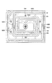
[0021]本発明は、基板支持アッセンブリと、大面積基板についてプロセスチャンバー内の基板の温度を制御する方法とを提供する。図2は、本発明の一実施形態によるプロセスチャンバー100を例示している。本発明は、カリフォルニア州サンタクララのアプライド・マテリアルズ・インクの一部門であるAKTから入手できるような大面積基板を処理するためのプラズマエンハンスト化学気相堆積プロセスチャンバーを参照して以下に説明する。しかしながら、本発明は、他のシステム構成、例えば、物理的気相堆積システム、イオンインプラントシステム、エッチングシステム、化学的気相堆積システム、及びプロセスチャンバー内の基板支持体上の基板の温度制御が望まれる他のシステムにも利用できることを理解されたい。
[0021] The present invention provides a substrate support assembly and a method for controlling the temperature of a substrate in a process chamber for large area substrates. FIG. 2 illustrates a
[0022]プロセスチャンバー100は、処理容積部140を部分的に画成する壁106及び底部108を有するチャンバー本体102を備えている。処理容積部140は、大面積ガラス基板のような基板112をプロセスチャンバー100に入れたり出したりするのを容易にするために、通常、ポート及びバルブ(図示せず)を通してアクセスされる。壁106は、蓋アッセンブリ110を支持し、これに収容されたポンピング充満部114は、処理容積部140を排出ポート(図示されていない種々のポンピング要素を含む)に結合し、ガス及びプロセス副産物をプロセスチャンバー100から排出させる。プロセスチャンバー100は、通常、1つ以上のソース化合物及び/又は先駆物質を送給するための1つ以上の供給源104、例えば、とりわけ、シリコン含有化合物供給源、酸素含有化合物供給源、水素ガス供給源、炭素含有化合物供給源、及び/又はその組合せに結合される。
The
[0023]基板支持アッセンブリ138は、一般に、チャンバー本体102の底部に配置される。この支持アッセンブリ138は、一般に、接地されており、電源122により蓋アッセンブリ110と基板支持アッセンブリ138との間に位置するガス分配プレートアッセンブリ118(又はプロセスチャンバー100の蓋アッセンブリ110内又はその付近に位置する他の電極)へ供給されるRF電力で、基板支持アッセンブリ138とガス分配プレートアッセンブリ118との間の処理容積部140に存在するガス、ソース化合物及び/又は先駆物質を励起させることができる。電源122からのRF電力は、一般に、化学気相堆積プロセスを推進するように基板112のサイズに適合するように選択される。一実施形態では、約400W以上、例えば、約2000W乃至約4000W、又は約10000W乃至約20000WのRF電力を電源122に印加して、処理容積部140に電界を発生することができる。例えば、本発明の低温基板堆積方法に適合するように、約0.2ワット/cm2以上、例えば、約0.2ワット/cm2乃至約0.8ワット/cm2、又は約0.45ワット/cm2の電力密度を使用することができる。電源122及びマッチングネットワーク(図示せず)は、処理容積部140内の先駆ガスからプロセスガスのプラズマを生成して維持する。13.56MHzの高周波RF電力を使用できるのが好ましいが、これは重要ではなく、それより低い周波数も使用できる。更に、チャンバーの壁は、セラミック材料又はアノード処理のアルミニウム材料で覆うことにより保護できる。
[0023] The
[0024]一般に、基板支持アッセンブリ138は、シャフト142に結合されると共に、リフトシステム(図示せず)に接続され、これは、基板支持アッセンブリ138を、上昇した処理位置(図示された)と、下降した基板移送位置との間で移動させる。シャフト142は、更に、基板支持アッセンブリ138と、プロセスチャンバー100の他の要素との間の電気リード及びサーモカップルリードのためのコンジットをなす。ベローズ146が基板支持アッセンブリ138に結合されて、処理容積部140とプロセスチャンバー100の外部の大気中との間に真空シールを与えると共に、基板支持アッセンブリ138の垂直移動を容易にする。基板支持アッセンブリ138のリフトシステムは、一般に、基板112とガス分配プレートアッセンブリ118との間の間隔が、処理中に、例えば、約400ミル以上の最適な大きさになるように調整される。この間隔を調整する能力は、広範囲な堆積条件にわたりプロセスを最適なものにする一方、大型基板の面積にわたり必要な膜均一性を維持できるようにする。
[0024] In general, the
[0025]基板支持アッセンブリ138は、基板処理中に処理容積部140内で基板112を支持するための基板支持面134を有する伝導性本体124を備えている。この伝導性本体124は、熱伝導率を与える金属又は金属合金材料で形成することができる。一実施形態において、伝導性本体124は、アルミニウム材料で作られる。しかしながら、他の適当な材料も使用できる。基板支持アッセンブリ138は、更に、基板処理中に基板支持面134に配置される基板112を取り巻くシャドーフレーム148も支持する。
[0025] The
[0026]一般的に、このシャドーフレーム148は、基板112及び基板支持アッセンブリ138の縁における堆積を防止して、基板112が支持アッセンブリ138にくっつかないようにする。シャドーフレーム148は、基板支持アッセンブリ138が下部の非処理位置(図示せず)にあるときにチャンバー本体102の内壁に沿って一般的に位置される。シャドーフレーム148は、基板支持アッセンブリ138が図2に示す上部の処理位置にあるときに、シャドーフレーム148の1つ以上の整列グルーブを1つ以上の整列ピン202に一致させることにより、基板支持アッセンブリ138の伝導性本体124に係合及び整列させることができる。1つ以上の整列ピン202は、伝導性本体124の周囲及びその付近に置かれた1つ以上の整列ピンホール204を通過するように適応される。1つ以上の整列ピン202は、任意であるが、基板ロード及びアンロードの間に伝導性本体124と共に移動できるように支持ピンプレート234により支持されてもよい。
[0026] Generally, the
[0027]温度制御される基板支持アッセンブリ138は、この基板支持アッセンブリ138及びこれに位置された基板112を所定の温度範囲、例えば、約100℃以上の設定点温度へ制御可能に加熱するために電源174に結合された1つ以上の電極及び/又は加熱素子132も備えることができる。一実施形態では、1つ以上の加熱素子132が伝導性本体124内に埋設される。
[0027] The temperature controlled
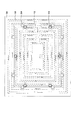
[0028]図3A−3Bは、本発明の1つ以上の態様に基づいて伝導性本体124に配置された1つ以上の加熱素子132の平面図である。例えば、図3Aに示すように、加熱素子132は、シャフト142を通して伝導性本体124に入り、伝導性本体124の中心領域の周りを1つ以上の内側ループで且つ伝導性本体124の外周を1つ以上の外側ループでループ形成し、次いで、シャフト142を通して出て、1つ以上の加熱素子132が伝導性本体124の大きさにわたって埋設されるようにする。
[0028] FIGS. 3A-3B are plan views of one or
[0029]更に、基板支持アッセンブリ138内に1つ以上のサーモカップル(図示せず)を使用することができる。一実施形態では、伝導性本体124の中心領域に対して1つと、外周に対して1つの、2つのサーモカップルが使用される。しかしながら、他のヒータ線又はチャンネル構成も使用できる。例えば、1つ以上の加熱素子132を伝導性本体124の背面に位置させるか、又はクランププレートにより伝導性本体124にクランプさせることもできる。1つ以上の加熱素子132は、約100℃以上の所定温度に抵抗性加熱されるか又は他の加熱手段で加熱されてもよい。
[0029] Additionally, one or more thermocouples (not shown) can be used in the
[0030]基板支持アッセンブリ138は、基板112を保持及び整列するように適応される付加的なメカニズムを備えてもよい。例えば、伝導性本体124は、複数の基板支持ピン222が貫通するための1つ以上の基板支持ピンホール224を含むことができ、これらは、伝導性本体124の僅かな距離上に基板112を支持するように適応される。基板支持ピン222は、プロセスチャンバー100の外部に配置された移送ロボット又は他の移送メカニズムにより、この移送ロボットの邪魔にならずに、基板112の配置又は除去を容易に行うために、基板112の周囲付近に位置させることができる。一実施形態では、基板支持ピン222は、基板処理中に電気的絶縁性を与えながらも熱伝導性であるように、とりわけ、セラミック材料、アノード処理された酸化アルミニウム材料のような絶縁材料で作ることができる。基板支持ピン222は、任意であるが、基板のロード及びアンロード中に基板112を持ち上げるために基板支持アッセンブリ138内を基板支持ピン222が移動できるように支持ピンプレート234により支持されてもよい。或いは又、基板支持ピン222をチャンバー底部に固定すると共に、基板支持ピン222が貫通するように伝導性本体124を垂直に移動可能としてもよい。
[0030] The
[0031]別の実施形態では、基板122が伝導性本体124の基板支持面134にのせられるときに、加熱素子132の少なくとも1つの外側ループが基板122の外周に整列するように構成される。例えば、伝導性本体124の寸法が基板112の寸法より大きいときには、加熱素子132の少なくとも1つの外側ループの位置は、伝導性本体124の1つ以上のピンホールの位置、例えば、基板支持ピンホール224又は整列ピンホール204の邪魔にならずに、基板112の周囲を包囲するように構成されてもよい。
In another embodiment, at least one outer loop of the
[0032]図3Bに示すように、本発明の一実施形態では、加熱素子132の少なくとも1つの外側ループは、基板112の外縁を取り巻くように位置される。好ましくは、加熱素子132の少なくとも1つの外側ループは、1つ以上の基板支持ピンホール224の位置、ひいては、基板112の縁を支持するための基板支持ピン222の位置の邪魔にならないように、伝導性本体124の中心から遠くに離れて、1つ以上の基板支持ピンホール224の周りに位置される。更に、本発明の別の実施形態では、加熱素子132の少なくとも1つの外側のループは、基板112の縁及び周囲へ加熱を与えるために、1つ以上の基板支持ピンホール224と伝導性本体124の外縁との間に位置される。
[0032] As shown in FIG. 3B, in one embodiment of the present invention, at least one outer loop of the
[0033]本発明の1つ以上の態様によれば、基板支持アッセンブリ138は、更に、伝導性本体124内に埋設された1つ以上の冷却チャンネル136も備えている。この1つ以上の冷却チャンネル136は、温度制御を維持すると共に、基板処理中に生じ得る温度変動、例えば、プロセスチャンバー100内にRFプラズマが発生したときの温度上昇又はスパイクを補償するように構成される。冷却チャンネル136の直径には、制限がなく、約1mm乃至約15mm、例えば、約9mmの適当な直径でよい。更に、冷却チャンネル136は、熱伝導率を与える金属又は金属合金材料で作ることができる。一実施形態では、冷却チャンネル136は、ステンレススチール材料で作られる。しかしながら、他の適当な材料構成を使用することもできる。
In accordance with one or more aspects of the present invention, the
[0034]冷却チャンネル136は、冷却流体、例えば、ガス状材料、水、冷却材、及び他の適当な冷却ガス又は液体材料を流すように適応される。好ましくは、ガス状材料が使用される。適当なガス状材料は、きれいな乾燥空気、圧縮空気、濾過された空気、窒素ガス、水素ガス、不活性ガス(例えば、アルゴンガス、ヘリウムガス、等)、及び他のガスを含むことができる。1つ以上の冷却チャンネル136内にガス状材料を流すことは、たとえ冷却水が便利に使用できても冷却水を流すより有益である。というのは、ガス状材料は、より広い温度範囲において冷却能力を発揮し、しかも、チャンバー要素や処理基板上の堆積膜のクオリティに影響するような水分漏れのおそれがないからである。例えば、約10℃ないし約25℃のガス状材料を使用して、1つ以上の冷却チャンネル136へ流し込み、室温から約200℃以上の高い温度までの温度冷却制御を与えることができるが、冷却水は、一般に、約20℃ないし約100℃で作用するだけである。
[0034] The
[0035]更に、冷却チャンネル136内を流れる冷却流体は、基板112が加熱素子132により加熱されるときの基板処理中に及び/又はチャンバーのアイドリング時間中に、冷却効率を制御するように、制御された流量で作用させることができる。例えば、直径が約9mmの例示的な冷却チャンネルの場合に、約25psi乃至約100psi、例えば、約50psiの圧力を使用して、ガス状冷却材料を流し込むことができる。従って、加熱素子132及び冷却チャンネル136を有する本発明の基板支持アッセンブリ138を使用すると、基板112の温度を一定に保持できると共に、基板112の大きな表面積全体にわたり均一な温度分布が維持される。
[0035] Further, the cooling fluid flowing in the
[0036]図4A−4Cは、基板支持アッセンブリ138の伝導性本体124に配置された加熱素子132及び冷却チャンネル136の構成を例示している。図4Aに示すように、冷却流体は、中央シャフトから流れ方向400Aに伝導性本体124に向かって延びる1つ以上の流入冷却チャンネルを通して伝導性本体124へ流れ込むことができ、ここで、1つ以上の流入冷却チャンネルは、伝導性本体124の周囲に向かって螺旋構成又は渦巻形状で延びる。
[0036] FIGS. 4A-4C illustrate the configuration of
[0037]次いで、図4Aに示すように、冷却流体は、流入冷却チャンネルから、流れ方向400Bに中心シャフトに向かって延びる1つ以上の流出冷却チャンネルへと流れ、ここで、1つ以上の流出冷却チャンネルは、伝導性本体124から螺旋構成で延びている。従って、全体的に、冷却チャンネル136は、一実施形態では、二重螺旋構成で構成することができ、流れ方向400A及び400Bで示すように、一方の螺旋は流入であり、他方の螺旋は流出である。更に、図4Aに示すように、冷却チャンネル136の隣接ループ即ちチャンネルは、流れ方向400A及び400Bで示すように、冷却流体を互いに逆方向に流すように構成される。
[0037] The cooling fluid then flows from the inflow cooling channel to one or more outflow cooling channels extending toward the central shaft in the
[0038]図4Bは、本発明の別の例示的冷却チャンネル及び加熱素子を示している。冷却チャンネル136は、シャフト142を通して伝導性本体124に入って、1つ以上の内側冷却ループ436Aを形成し、加熱素子132の1つ以上の内側ループの周りにループ形成するように構成される。また、冷却チャンネル136は、1つ以上の外側冷却ループ436Bを形成して、伝導性本体124の外周付近で加熱素子132の1つ以上の外側ループの周りにループ形成するように構成される。次いで、冷却チャンネル136は、シャフト142を通して出ることができる。一実施形態では、冷却チャンネル136の内側冷却ループ436A及び外側冷却ループ436Bは、螺旋、渦巻き構成で構成される。例えば、内側冷却ループ436A及び外側冷却ループ436Bは、伝導性本体124の中心部分から、伝導性本体124の周囲に向かい、次いで、基板支持アッセンブリ138のシャフト142の中心部分へループ形成して戻るように構成される。別の実施形態では、冷却チャンネル136の内側冷却ループ436A及び外側冷却ループ436Bは、基板支持ピン222が貫通するように構成された1つ以上の基板支持ピンホール224から離間され、伝導性本体124の1つ以上の基板支持ピンホール224の位置に邪魔にならないように適応される。
[0038] FIG. 4B illustrates another exemplary cooling channel and heating element of the present invention. The cooling
[0039]図4Cは、本発明の1つ以上の態様による別の例示的冷却チャンネル構成を示している。1つ以上の冷却チャンネルは、図4Cに矢印で示す流れ方向にループ形成する螺旋相互ループ「C」構成で構成することができる。従って、冷却チャンネル136を、伝導性本体124の寸法にわたって分布させることができる。
[0039] FIG. 4C illustrates another exemplary cooling channel configuration in accordance with one or more aspects of the present invention. One or more cooling channels may be configured in a helical inter-loop “C” configuration that loops in the flow direction indicated by the arrows in FIG. 4C. Accordingly, the cooling
[0040]図5は、本発明の1つ以上の態様による断面A−Aにわたる断面図である。図5に示すように、本発明の一実施形態では、冷却チャンネル136は、加熱素子132の上に位置されて、基板支持アッセンブリ138の伝導性本体124内に充分な温度制御を与えるように構成される。加熱素子132は、コイル510と、何らかの付加的な絶縁材料520とを含むことができる。更に、1つ以上の加熱素子132及び1つ以上の冷却チャンネル136のためのループ、管路又はチャンネルは、とりわけ、溶接、サンドブラスト、高圧ボンディング、接着剤ボンディング、鍛造のような既知のボンディング技術を使用して、基板支持アッセンブリ138の伝導性本体124に製造し及びボンディングすることができる。
[0040] FIG. 5 is a cross-sectional view across section AA according to one or more aspects of the present invention. As shown in FIG. 5, in one embodiment of the present invention, the cooling
[0041]一実施形態では、冷却チャンネル136のループ、管路及び/又はチャンネルを加熱素子132のチャンネル及び/又はループの周りに位置させて、冷却チャンネル136を伝導性本体124の寸法にわたって分布させることができるように構成される。例えば、図5に示すように、冷却チャンネル136の少なくとも2つ以上のループが、加熱素子132の1つのチャンネルの上に埋設される。好ましくは、加熱素子132の1つのチャンネルの上にある冷却チャンネル136の2つ以上のループは、互いに逆の流れ方向400A及び400Bに流れるガス状材料を含む。
[0041] In one embodiment, the loops, conduits and / or channels of the
[0042]従って、1つ以上の加熱素子132及び1つ以上の冷却チャンネル136が基板支持アッセンブリ138に配置されて、基板112を400℃以下の均一温度、例えば、約100℃乃至約200℃に維持する。加熱素子132の加熱効率は、電源174により調整することができ、また、冷却チャンネル136の冷却効率は、そこに流れるガス状材料の流量により調整することができ、加熱−冷却の二通りの制御が達成される。
[0042] Accordingly, one or
[0043]その結果、基板支持アッセンブリ138及びそこに位置される基板112は、常に、所定の設定点温度に制御可能に維持される。本発明の基板支持アッセンブリを使用すると、基板支持アッセンブリ138の伝導性本体124に対して、設定点温度の約±5℃以下の温度均一性を観察することができる。プロセスチャンバーにより多数の基板が処理された後でも、約±2℃以下というプロセス設定点温度反復性を観察することができる。一実施形態では、基板112の温度が一定に保たれ、正規化された温度変動は、約±10℃、例えば、約±5℃の温度変動である。
[0043] As a result, the
[0044]更に、伝導性本体124の下にベース支持プレートを位置させ、基板支持アッセンブリ138及びその上の基板112に構造上の支持を与えて、それらが重力や高温度のためにそれるのを防止すると共に、伝導性本体124と基板112との間に比較的均一で且つ反復性のある接触を確保することができる。従って、本発明の基板支持アッセンブリ138の伝導性本体124は、静電チャックを使用せずに大面積基板の温度を制御するための加熱及び冷却能力を伴う簡単な設計を提供する。というのは、真空チャックに対して基板の裏側に圧力、ガス又は流体を印加すると、大面積ガラス基板は、容易にガラスの割れを招くことがあるからである。
[0044] In addition, a base support plate is positioned under the
[0045]図2に戻ると、蓋アッセンブリ110は、通常、入口ポート180を備え、これを通して、供給源104により供給されるプロセスガスがプロセスチャンバー100へ導入される。また、入口ポート180は、洗浄剤源182にも結合され、これは、解離したフッ素のような洗浄剤をプロセスチャンバー100へ供給して、ガス分配プレートアッセンブリ118を含むプロセスチャンバーハードウェアから堆積副産物及び膜を除去する。
Returning to FIG. 2, the
[0046]ガス分配プレートアッセンブリ118は、通常、例えば、大面積基板については長方形で、ウェハについては円形の、基板112のプロフィールに実質的に従うように構成される。ガス分配プレートアッセンブリ118は、穿孔エリア116を備え、これを通して、供給源104から供給される先駆ガス及び他のガス、例えば、水素ガスが処理容積部140へ配送される。穿孔エリア116は、ガス分配プレートアッセンブリ118を通してプロセスチャンバー100へ至るガスの均一な分配を与えるように構成される。ガス分配プレートアッセンブリ118は、通常、ハンガープレート160から懸架された拡散プレート158を備えている。拡散プレート158を貫通して複数のガス通路162が形成され、ガス分配プレートアッセンブリ118を通して処理容積部140へ至るガスの所定の分配を許容する。
[0046] The gas
[0047]プロセスチャンバー100の種々の要素にインターフェイスしそしてそれらを制御するためにコントローラ190が含まれる。このコントローラ190は、通常、中央処理ユニット(CPU)194と、サポート回路196と、メモリ192とを備えている。CPU194は、種々のチャンバー、装置、及びチャンバー周辺機器を制御するための工業用設定に使用できる任意の形式のコンピュータプロセッサの1つでよい。CPU194に結合されるメモリ192、任意のソフトウェア、又はコンピュータ読み取り可能な媒体は、1つ以上の容易に入手できるメモリデバイス、例えば、ランダムアクセスメモリ(RAM)、リードオンリメモリ(ROM)、ハードディスク、CD、フロッピーディスク、又は他の形式のデジタル記憶装置を、メモリ記憶装置のためのローカル又はリモート用として含むことができる。サポート回路196は、CPU194を従来の仕方でサポートするためにCPU194に結合される。これらの回路は、キャッシュ、電源、クロック回路、入力/出力回路、サブシステム、等を含む。
[0047] A
[0048]一実施形態において、本発明のプロセスチャンバー100の基板支持アッセンブリ138は、長方形基板を処理するように適応される。フラットパネルディスプレイ用の長方形基板の表面積は、通常、大きく、例えば、約300mmx約400mm以上、例えば、約370mmx約470mm以上の長方形である。チャンバー本体102、伝導性本体124、及びプロセスチャンバー100の関連要素の寸法には、限度がなく、一般的に、プロセスチャンバー100で処理されるべき基板112のサイズ及び寸法より比例的に大きい。例えば、幅が約370mm乃至約2160mmで、長さが約470mm乃至約2460mmの大面積の方形の基板を処理するときには、伝導性本体は、幅が約430mm乃至約2300mmで、長さが約520mm乃至約2600mmでよく、一方、チャンバー本体102は、幅が約570mm乃至約2360mmで、長さが約570mm乃至約2660mmでよい。
[0048] In one embodiment, the
[0049]フラットパネルディスプレイの用途では、基板112は、可視スペクトルにおいて本質的に光学的に透明な材料、例えば、ガラス又は透明プラスチックで構成することができる。例えば、薄膜トランジスタの用途では、基板112は、高度の光学的透明性を有する大面積ガラス基板でよい。しかしながら、本発明は、任意の形式及びサイズの基板処理にも等しく適用できる。本発明の基板は、フラットパネルディスプレイ製造用の円形、方形、長方形、又は多角形でよい。更に、本発明は、フラットパネルディスプレイ(FPD)、フレキシブルディスプレイ、有機発光ダイオード(OLED)ディスプレイ、フレキシブル有機発光ダイオード(FOLED)ディスプレイ、ポリマー発光ダイオード(PLED)ディスプレイ、液晶ディスプレイ(LCD)、有機薄膜トランジスタ、能動的マトリクス、受動的マトリクス、頂面放射デバイス、底面放射デバイス、太陽電池、太陽パネル、等のデバイスを製造するための基板に適用されると共に、とりわけ、シリコンウェハ、ガラス基板、金属基板、プラスチック膜(例えば、ポリエチレンテレフタレート(PET)、ポリエチレンナフサレート(PEN)、等)、プラスチックエポキシ膜のいずれに適用することもできる。本発明は、低温PECVDプロセス、例えば、基板処理中に温度冷却制御が望まれるフレキシブルディスプレイ装置を製造するのに使用される技術に特に適している。
[0049] For flat panel display applications, the
[0050]図6は、プロセスチャンバー内の基板の温度を制御するための1つの例示的方法600を示すフローチャートである。運転中に、ステップ610において、プロセスチャンバー内の基板支持アッセンブリの基板支持面に基板が位置される。基板処理前に及び/又はその間に、基板支持アッセンブリの伝導性本体の頂部の基板支持面の温度が、設定点温度、例えば、約100℃ないし約200℃に保持される。ステップ620において、基板支持アッセンブリの伝導性本体に埋設された1つ以上の冷却チャンネルに冷却ガス又は空気が一定の流量で流し込まれる。
[0050] FIG. 6 is a flowchart illustrating one
[0051]一実施形態では、冷却ガスは、チャンバーのアイドリング時間、非処理時間、又はチャンバーの洗浄/保守時間中にも、冷却チャンネルに流し込むことができる。その結果、本発明の1つ以上の冷却チャンネルは、常にアクティブとなる。別の実施形態では、チャンバーのアイドリング時間中に使用される設定点温度は、基板処理中に設定される処理温度と同じ温度である。 [0051] In one embodiment, the cooling gas may flow into the cooling channel during chamber idle time, non-treatment time, or chamber cleaning / maintenance time. As a result, one or more cooling channels of the present invention are always active. In another embodiment, the set point temperature used during the chamber idle time is the same temperature as the process temperature set during substrate processing.
[0052]ステップ630において、基板の温度は、基板支持アッセンブリの伝導性本体に埋設された1つ以上の加熱素子の加熱効率を調整することにより基板処理中に一定に維持される。例えば、加熱素子の加熱効率は、加熱素子に接続された電源の電力を調整することにより調整できる。一実施形態では、基板の温度は、プラズマを誘起するか、或いはプラズマのエネルギーから発生される付加的な熱を基板に向けて、基板の表面の温度スパイク又は変動を防止するかどうかに関わらず、加熱素子に対する電源の電力を微同調することにより、基板の全面にわたり約100℃ないし約200度の一定処理温度に維持することができる。その結果、加熱及び冷却の両方の効率を調整するためのより複雑な2つ以上の制御ループに比して、加熱効率を調整するための1つの制御ループが、コントローラ190内のソフトウェア設計として必要とされるだけである。従って、本発明の方法600は、基板支持アッセンブリに対する加熱効率を制御することにより簡単で且つ信頼性のある温度制御メカニズムを提供する。しかしながら、本発明の基板支持アッセンブリ138は、加熱及び/又は冷却効率を調整することができる。
[0052] In
[0053]運転中に、基板支持アッセンブリの1つ以上の加熱素子は、約150℃の設定点温度に設定することができ、また、温度が約16℃のきれいな乾燥空気又は圧縮空気のガス状冷却材料を冷却チャンネルに一定流量で流し込んで、基板支持アッセンブリの基板支持面の温度を維持することができる。プラズマ又は付加的な熱源がプロセスチャンバー内で基板支持面の頂部付近に存在するときには、約±2℃の表面温度均一性で基板支持面の温度を約150℃に一定に維持するために、約50psiの圧力を使用して冷却材料の一定流がテストされる。約300℃の付加的な熱源が存在しても、基板支持面の温度には影響しないことがテストされ、基板支持面は、本発明の冷却チャンネル内に導入温度が約16℃の冷却流体を流すことにより約150℃に一定に保持されることがテストされている。冷却ガスは、基板支持アッセンブリを冷却してそこから流出された後に、約120℃の放出温度であることがテストされている。それ故、本発明の冷却チャンネル内に流れる冷却ガスは、冷却ガスの放出温度と導入温度との間の差が100℃を越えることで表わされる非常に効率的な冷却作用を示している。 [0053] During operation, one or more heating elements of the substrate support assembly can be set to a set point temperature of about 150 ° C. and the temperature of clean dry or compressed air at a temperature of about 16 ° C. A cooling material can be flowed into the cooling channel at a constant flow rate to maintain the temperature of the substrate support surface of the substrate support assembly. When a plasma or additional heat source is present in the process chamber near the top of the substrate support surface, in order to maintain the substrate support surface temperature constant at about 150 ° C. with a surface temperature uniformity of about ± 2 ° C., about A constant flow of cooling material is tested using a pressure of 50 psi. The presence of an additional heat source of about 300 ° C. has been tested to not affect the temperature of the substrate support surface, and the substrate support surface has a cooling fluid with an introduction temperature of about 16 ° C. in the cooling channel of the present invention. It has been tested to be held constant at about 150 ° C. by flowing. The cooling gas has been tested to have a discharge temperature of about 120 ° C. after cooling the substrate support assembly and flowing out of it. Therefore, the cooling gas flowing in the cooling channel of the present invention exhibits a very efficient cooling action which is represented by the difference between the discharge temperature of the cooling gas and the introduction temperature exceeding 100 ° C.
[0054]本発明の教示を組み込んだ多数の好ましい実施形態を図示して詳細に説明したが、当業者であれば、これらの教示を組み込んだ多数の他の変形実施形態も容易に案出できよう。以上の説明は、本発明の実施形態に向けられたが、本発明の基本的な範囲から逸脱せずに、本発明の他の及び更に別の実施形態を案出することもでき、本発明の範囲は、特許請求の範囲により決定される。 [0054] While a number of preferred embodiments incorporating the teachings of the present invention have been illustrated and described in detail, those skilled in the art can readily devise many other variations that incorporate these teachings. Like. Although the foregoing description has been directed to embodiments of the invention, other and further embodiments of the invention may be devised without departing from the basic scope of the invention. Is determined by the claims.
2…プロセスチャンバー、8…側壁、10…開口、12…基板、14…ガス入口、16…拡散プレート、18…支持プレート、20…支持シャフト、22…サセプタ、24…電源、34…距離、36…大きな距離、100…プロセスチャンバー、102…チャンバー本体、104…供給源、106…壁、108…底部、110…蓋アッセンブリ、112…基板、114…ポンピング充満部、116…穿孔エリア、118…ガス分配プレートアッセンブリ、122…電源、124…伝導性本体、132…加熱素子、134…基板支持面、136…冷却チャンネル、138…基板支持アッセンブリ、140…処理容積部、142…シャフト、146…ベローズ、148…シャドーフレーム、158…拡散プレート、160…ハンガープレート、162…ガス通路、174…電源、180…入口ポート、182…洗浄剤源、190…コントローラ、192…メモリ、194…CPU、196…サポート回路、202…整列ピン、204…整列ピンホール、222…基板支持ピン、224…基板支持ピンホール、234…支持ピンプレート、400A…流れ方向、400B…流れ方向、436A…内側冷却ループ、436B…外側冷却ループ、510…コイル、520…絶縁材料、600…方法、610…ステップ、620…ステップ、630…ステップ
2 ... Process chamber, 8 ... Side wall, 10 ... Opening, 12 ... Substrate, 14 ... Gas inlet, 16 ... Diffusion plate, 18 ... Support plate, 20 ... Support shaft, 22 ... Susceptor, 24 ... Power source, 34 ... Distance, 36 ... large distance, 100 ... process chamber, 102 ... chamber body, 104 ... source, 106 ... wall, 108 ... bottom, 110 ... lid assembly, 112 ... substrate, 114 ... pumping filling, 116 ... perforation area, 118 ... gas Distribution plate assembly, 122 ... Power source, 124 ... Conductive body, 132 ... Heating element, 134 ... Substrate support surface, 136 ... Cooling channel, 138 ... Substrate support assembly, 140 ... Processing volume, 142 ... Shaft, 146 ... Bellows, 148 ... Shadow frame, 158 ... Diffusion plate, 160 ... Hanger plate, 1 DESCRIPTION OF
Claims (17)
1つ以上の基板支持ピンホールを有する1つの熱伝導性本体であって、金属又は金属合金材料で形成される熱伝導性本体と、
上記熱伝導性本体の表面にあって、そこに上記基板を支持するように適応される基板支持面と、
上記熱伝導性本体内に埋設された1つ以上の加熱素子と、
上記熱伝導性本体内で上記1つ以上の加熱素子の周りに埋設された1つ以上の冷却チャンネルであって、上記1つ以上の冷却チャンネルは冷却流体を流すように適応された冷却チャンネルと、を備え、
上記1つ以上の冷却チャンネルは、上記基板支持ピンホールから離れて配置された内側冷却ループ及び外側冷却ループからなる渦巻状構造を形成し、上記内側冷却ループ及び外側冷却ループは、上記熱伝導性本体の中心部分から、上記熱伝導性本体の周囲に向かい、次いで、上記熱伝導性本体の中心部分へ戻るようにループ形成され、
隣接する上記内側冷却ループ及び上記外側冷却ループは、冷却流体を互いに逆方向に流すように構成される基板支持アッセンブリ。 In a substrate support assembly adapted to support a substrate in a process chamber,
A thermally conductive body having one or more substrate support pinholes, the thermally conductive body formed of a metal or metal alloy material;
A substrate support surface on the surface of the thermally conductive body and adapted to support the substrate thereon;
One or more heating elements embedded in the thermally conductive body;
One or more cooling channels embedded around the one or more heating elements in the thermally conductive body, wherein the one or more cooling channels are adapted to flow cooling fluid ; With
The one or more cooling channels form a spiral structure consisting of an inner cooling loop and an outer cooling loop disposed away from the substrate support pinhole, wherein the inner cooling loop and the outer cooling loop Looped from a central portion of the body toward the periphery of the thermally conductive body and then back to the central portion of the thermally conductive body;
The substrate support assembly, wherein the adjacent inner cooling loop and the outer cooling loop are configured to flow cooling fluids in opposite directions.
金属又は金属合金材料で形成される1つの熱伝導性本体と、
上記熱伝導性本体の表面にあって、そこに上記ガラス基板を支持するように適応される基板支持面と、
上記熱伝導性本体内に埋設された1つ以上の加熱素子と、
上記熱伝導性本体内の上記1つ以上の加熱素子の周りに埋設された1つ以上の冷却チャンネルであって、上記1つ以上の冷却チャンネルは冷却流体を流すように適応され、上記熱伝導性本体の中心部分から、上記熱伝導性本体の周囲に向かい、次いで、上記熱伝導性本体の中心部分へ戻るようにループ形成された1つ以上の冷却チャンネルと、を備え、
上記1つ以上の冷却チャンネルの隣接チャンネルが、冷却流体を互いに逆方向に流すように構成される基板支持アッセンブリ。 In a substrate support assembly adapted to support a glass substrate within a process chamber,
One thermally conductive body formed of a metal or metal alloy material;
A substrate support surface on the surface of the thermally conductive body and adapted to support the glass substrate therein;
One or more heating elements embedded in the thermally conductive body;
One or more cooling channels embedded around the one or more heating elements in the thermally conductive body, wherein the one or more cooling channels are adapted to flow a cooling fluid; One or more cooling channels looped from a central portion of the conductive body toward the periphery of the thermally conductive body and then back to the central portion of the thermally conductive body;
A substrate support assembly, wherein adjacent channels of the one or more cooling channels are configured to flow cooling fluids in opposite directions.
上記プロセスチャンバーの基板支持アッセンブリの基板支持面に上記基板を位置させるステップであって、上記基板支持アッセンブリは、
金属又は金属合金材料で形成される1つの熱伝導性本体、
上記熱伝導性本体の表面にあって、そこに上記基板を支持するように適応される基板支持面、
上記熱伝導性本体内に埋設された1つ以上の加熱素子、及び
上記熱伝導性本体内に埋設され、上記1つ以上の加熱素子の周りに位置された1つ以上の冷却チャンネルであって、上記1つ以上の冷却チャンネルは冷却流体を流すように適応され、内側冷却ループ及び外側冷却ループからなる渦巻状構造を形成し、上記熱伝導性本体の中心部分から、上記熱伝導性本体の周囲に向かい、次いで、上記熱伝導性本体の中心部分へ戻るようにループ形成され、隣接する上記内側冷却ループ及び上記外側冷却ループは、冷却流体を互いに逆方向に流すように構成されるチャンネルを含む、
基板支持アッセンブリであるようなステップと、
上記1つ以上の冷却チャンネル内にガス状の冷却材を流すステップと、
上記1つ以上の加熱素子の加熱電力を調整することにより上記基板の温度を、設定点温度における±5℃以下の温度均一性で、当該設定点温度に維持するステップと、を備えた方法。 In a method for maintaining the temperature of a substrate within a process chamber,
Positioning the substrate on a substrate support surface of a substrate support assembly of the process chamber, the substrate support assembly comprising:
One thermally conductive body formed of a metal or metal alloy material;
A substrate support surface on the surface of the thermally conductive body and adapted to support the substrate thereon;
One or more heating elements embedded in the thermally conductive body, and one or more cooling channels embedded in the thermally conductive body and positioned around the one or more heating elements, The one or more cooling channels are adapted to flow a cooling fluid to form a spiral structure comprising an inner cooling loop and an outer cooling loop, from a central portion of the thermally conductive body, Looped to the periphery and then back to the central portion of the thermally conductive body, the adjacent inner and outer cooling loops have channels configured to flow cooling fluids in opposite directions. Including,
A step that is a substrate support assembly;
Flowing a gaseous coolant through the one or more cooling channels;
Maintaining the temperature of the substrate at the set point temperature with temperature uniformity of ± 5 ° C. or less at the set point temperature by adjusting the heating power of the one or more heating elements.
The method of claim 15, wherein the one or more cooling channels comprise gaseous material having a temperature between 10 ° C. and 25 ° C. flowing therein.
Applications Claiming Priority (2)
| Application Number | Priority Date | Filing Date | Title |
|---|---|---|---|
| US11/206,245 US8709162B2 (en) | 2005-08-16 | 2005-08-16 | Active cooling substrate support |
| US11/206245 | 2005-08-16 |
Publications (3)
| Publication Number | Publication Date |
|---|---|
| JP2007053382A JP2007053382A (en) | 2007-03-01 |
| JP2007053382A5 JP2007053382A5 (en) | 2011-04-07 |
| JP5484650B2 true JP5484650B2 (en) | 2014-05-07 |
Family
ID=37766516
Family Applications (1)
| Application Number | Title | Priority Date | Filing Date |
|---|---|---|---|
| JP2006222039A Active JP5484650B2 (en) | 2005-08-16 | 2006-08-16 | Active cooling of substrate support |
Country Status (5)
| Country | Link |
|---|---|
| US (1) | US8709162B2 (en) |
| JP (1) | JP5484650B2 (en) |
| KR (1) | KR101312676B1 (en) |
| CN (1) | CN1919768B (en) |
| TW (1) | TWI338319B (en) |
Families Citing this family (341)
| Publication number | Priority date | Publication date | Assignee | Title |
|---|---|---|---|---|
| US8709162B2 (en) * | 2005-08-16 | 2014-04-29 | Applied Materials, Inc. | Active cooling substrate support |
| US7655542B2 (en) * | 2006-06-23 | 2010-02-02 | Applied Materials, Inc. | Methods and apparatus for depositing a microcrystalline silicon film for photovoltaic device |
| US7901509B2 (en) * | 2006-09-19 | 2011-03-08 | Momentive Performance Materials Inc. | Heating apparatus with enhanced thermal uniformity and method for making thereof |
| US20080173350A1 (en) * | 2007-01-18 | 2008-07-24 | Applied Materials, Inc. | Multi-junction solar cells and methods and apparatuses for forming the same |
| US8203071B2 (en) | 2007-01-18 | 2012-06-19 | Applied Materials, Inc. | Multi-junction solar cells and methods and apparatuses for forming the same |
| US7582515B2 (en) * | 2007-01-18 | 2009-09-01 | Applied Materials, Inc. | Multi-junction solar cells and methods and apparatuses for forming the same |
| US20080245414A1 (en) * | 2007-04-09 | 2008-10-09 | Shuran Sheng | Methods for forming a photovoltaic device with low contact resistance |
| US20080299326A1 (en) * | 2007-05-30 | 2008-12-04 | Asm Japan K.K. | Plasma cvd apparatus having non-metal susceptor |
| US7875486B2 (en) * | 2007-07-10 | 2011-01-25 | Applied Materials, Inc. | Solar cells and methods and apparatuses for forming the same including I-layer and N-layer chamber cleaning |
| US20090104733A1 (en) * | 2007-10-22 | 2009-04-23 | Yong Kee Chae | Microcrystalline silicon deposition for thin film solar applications |
| CN101842875A (en) * | 2007-11-02 | 2010-09-22 | 应用材料股份有限公司 | Plasma treatment between deposition processes |
| US20090130827A1 (en) * | 2007-11-02 | 2009-05-21 | Soo Young Choi | Intrinsic amorphous silicon layer |
| US7833885B2 (en) | 2008-02-11 | 2010-11-16 | Applied Materials, Inc. | Microcrystalline silicon thin film transistor |
| US8076222B2 (en) * | 2008-02-11 | 2011-12-13 | Applied Materials, Inc. | Microcrystalline silicon thin film transistor |
| KR101444711B1 (en) * | 2008-05-23 | 2014-09-26 | 주성엔지니어링(주) | Temperatute control system for substrate manufacturing apparatus |
| US8596336B2 (en) * | 2008-06-03 | 2013-12-03 | Applied Materials, Inc. | Substrate support temperature control |
| JP2010016225A (en) * | 2008-07-04 | 2010-01-21 | Tokyo Electron Ltd | Thermal control mechanism and semiconductor manufacturing device using the same |
| US8895842B2 (en) * | 2008-08-29 | 2014-11-25 | Applied Materials, Inc. | High quality TCO-silicon interface contact structure for high efficiency thin film silicon solar cells |
| US20100116788A1 (en) * | 2008-11-12 | 2010-05-13 | Lam Research Corporation | Substrate temperature control by using liquid controlled multizone substrate support |
| US20100184290A1 (en) * | 2009-01-16 | 2010-07-22 | Applied Materials, Inc. | Substrate support with gas introduction openings |
| JP5705133B2 (en) * | 2009-02-04 | 2015-04-22 | マットソン テクノロジー インコーポレイテッドMattson Technology, Inc. | Electrostatic chuck system and method for radially adjusting a temperature profile across a substrate surface |
| US20110114177A1 (en) * | 2009-07-23 | 2011-05-19 | Applied Materials, Inc. | Mixed silicon phase film for high efficiency thin film silicon solar cells |
| WO2011046664A2 (en) * | 2009-10-15 | 2011-04-21 | Applied Materials, Inc. | A barrier layer disposed between a substrate and a transparent conductive oxide layer for thin film silicon solar cells |
| US20110126875A1 (en) * | 2009-12-01 | 2011-06-02 | Hien-Minh Huu Le | Conductive contact layer formed on a transparent conductive layer by a reactive sputter deposition |
| US9267742B2 (en) | 2010-01-27 | 2016-02-23 | Applied Materials, Inc. | Apparatus for controlling the temperature uniformity of a substrate |
| US20110180233A1 (en) * | 2010-01-27 | 2011-07-28 | Applied Materials, Inc. | Apparatus for controlling temperature uniformity of a showerhead |
| JP2011181599A (en) * | 2010-02-26 | 2011-09-15 | Mitsubishi Heavy Ind Ltd | Apparatus and method for plasma film-forming |
| US10283321B2 (en) | 2011-01-18 | 2019-05-07 | Applied Materials, Inc. | Semiconductor processing system and methods using capacitively coupled plasma |
| WO2012134605A1 (en) * | 2011-03-25 | 2012-10-04 | Applied Materials, Inc. | Method and apparatus for thermocouple installation or replacement in a substrate support |
| WO2013009505A2 (en) | 2011-07-13 | 2013-01-17 | Applied Materials, Inc. | Methods of manufacturing thin film transistor devices |
| US20130023129A1 (en) | 2011-07-20 | 2013-01-24 | Asm America, Inc. | Pressure transmitter for a semiconductor processing environment |
| CN103828061B (en) | 2011-10-07 | 2018-02-13 | 应用材料公司 | Carry out the method for deposit silicon-containing materials using argon-dilution |
| US9234857B2 (en) | 2011-11-14 | 2016-01-12 | First Solar, Inc. | Method and apparatus providing temperature uniformity |
| US8900364B2 (en) * | 2011-11-29 | 2014-12-02 | Intermolecular, Inc. | High productivity vapor processing system |
| US20130284372A1 (en) * | 2012-04-25 | 2013-10-31 | Hamid Tavassoli | Esc cooling base for large diameter subsrates |
| US9089007B2 (en) * | 2012-04-27 | 2015-07-21 | Applied Materials, Inc. | Method and apparatus for substrate support with multi-zone heating |
| US9267739B2 (en) | 2012-07-18 | 2016-02-23 | Applied Materials, Inc. | Pedestal with multi-zone temperature control and multiple purge capabilities |
| US9132436B2 (en) | 2012-09-21 | 2015-09-15 | Applied Materials, Inc. | Chemical control features in wafer process equipment |
| US10714315B2 (en) | 2012-10-12 | 2020-07-14 | Asm Ip Holdings B.V. | Semiconductor reaction chamber showerhead |
| US10727092B2 (en) * | 2012-10-17 | 2020-07-28 | Applied Materials, Inc. | Heated substrate support ring |
| US20160376700A1 (en) | 2013-02-01 | 2016-12-29 | Asm Ip Holding B.V. | System for treatment of deposition reactor |
| US10256079B2 (en) | 2013-02-08 | 2019-04-09 | Applied Materials, Inc. | Semiconductor processing systems having multiple plasma configurations |
| TWI473903B (en) * | 2013-02-23 | 2015-02-21 | Hermes Epitek Corp | Gas Injector and Cover Plate Assembly for Semiconductor Equipment |
| US9406653B2 (en) | 2013-02-27 | 2016-08-02 | Applied Materials, Inc. | Integrated solution for solid state light sources in a process chamber |
| US9362130B2 (en) | 2013-03-01 | 2016-06-07 | Applied Materials, Inc. | Enhanced etching processes using remote plasma sources |
| JP5980147B2 (en) * | 2013-03-08 | 2016-08-31 | 日本発條株式会社 | Substrate support device |
| US10403521B2 (en) * | 2013-03-13 | 2019-09-03 | Applied Materials, Inc. | Modular substrate heater for efficient thermal cycling |
| USD717113S1 (en) * | 2013-03-13 | 2014-11-11 | Applied Materials, Inc. | Susceptor with heater |
| US11015245B2 (en) | 2014-03-19 | 2021-05-25 | Asm Ip Holding B.V. | Gas-phase reactor and system having exhaust plenum and components thereof |
| US9779971B2 (en) * | 2014-04-11 | 2017-10-03 | Applied Materials, Inc. | Methods and apparatus for rapidly cooling a substrate |
| US9309598B2 (en) | 2014-05-28 | 2016-04-12 | Applied Materials, Inc. | Oxide and metal removal |
| US10941490B2 (en) | 2014-10-07 | 2021-03-09 | Asm Ip Holding B.V. | Multiple temperature range susceptor, assembly, reactor and system including the susceptor, and methods of using the same |
| US9966240B2 (en) | 2014-10-14 | 2018-05-08 | Applied Materials, Inc. | Systems and methods for internal surface conditioning assessment in plasma processing equipment |
| US9355922B2 (en) | 2014-10-14 | 2016-05-31 | Applied Materials, Inc. | Systems and methods for internal surface conditioning in plasma processing equipment |
| US11637002B2 (en) | 2014-11-26 | 2023-04-25 | Applied Materials, Inc. | Methods and systems to enhance process uniformity |
| US10573496B2 (en) | 2014-12-09 | 2020-02-25 | Applied Materials, Inc. | Direct outlet toroidal plasma source |
| US10224210B2 (en) | 2014-12-09 | 2019-03-05 | Applied Materials, Inc. | Plasma processing system with direct outlet toroidal plasma source |
| US11257693B2 (en) | 2015-01-09 | 2022-02-22 | Applied Materials, Inc. | Methods and systems to improve pedestal temperature control |
| US9728437B2 (en) | 2015-02-03 | 2017-08-08 | Applied Materials, Inc. | High temperature chuck for plasma processing systems |
| US20160225652A1 (en) | 2015-02-03 | 2016-08-04 | Applied Materials, Inc. | Low temperature chuck for plasma processing systems |
| US10276355B2 (en) | 2015-03-12 | 2019-04-30 | Asm Ip Holding B.V. | Multi-zone reactor, system including the reactor, and method of using the same |
| US10458018B2 (en) | 2015-06-26 | 2019-10-29 | Asm Ip Holding B.V. | Structures including metal carbide material, devices including the structures, and methods of forming same |
| US9691645B2 (en) | 2015-08-06 | 2017-06-27 | Applied Materials, Inc. | Bolted wafer chuck thermal management systems and methods for wafer processing systems |
| US9741593B2 (en) | 2015-08-06 | 2017-08-22 | Applied Materials, Inc. | Thermal management systems and methods for wafer processing systems |
| US9349605B1 (en) | 2015-08-07 | 2016-05-24 | Applied Materials, Inc. | Oxide etch selectivity systems and methods |
| US10504700B2 (en) | 2015-08-27 | 2019-12-10 | Applied Materials, Inc. | Plasma etching systems and methods with secondary plasma injection |
| US10211308B2 (en) | 2015-10-21 | 2019-02-19 | Asm Ip Holding B.V. | NbMC layers |
| US10586718B2 (en) * | 2015-11-11 | 2020-03-10 | Applied Materials, Inc. | Cooling base with spiral channels for ESC |
| US11139308B2 (en) | 2015-12-29 | 2021-10-05 | Asm Ip Holding B.V. | Atomic layer deposition of III-V compounds to form V-NAND devices |
| JP6077147B2 (en) * | 2016-01-21 | 2017-02-08 | Sppテクノロジーズ株式会社 | Plasma substrate processing apparatus, control program thereof, and computer-readable recording medium recording the same |
| US10529554B2 (en) | 2016-02-19 | 2020-01-07 | Asm Ip Holding B.V. | Method for forming silicon nitride film selectively on sidewalls or flat surfaces of trenches |
| US10280510B2 (en) * | 2016-03-28 | 2019-05-07 | Applied Materials, Inc. | Substrate support assembly with non-uniform gas flow clearance |
| CN105734494B (en) * | 2016-04-12 | 2018-12-25 | 京东方科技集团股份有限公司 | A kind of vapor deposition support plate and evaporation coating device |
| US10367080B2 (en) | 2016-05-02 | 2019-07-30 | Asm Ip Holding B.V. | Method of forming a germanium oxynitride film |
| US10522371B2 (en) | 2016-05-19 | 2019-12-31 | Applied Materials, Inc. | Systems and methods for improved semiconductor etching and component protection |
| US10504754B2 (en) | 2016-05-19 | 2019-12-10 | Applied Materials, Inc. | Systems and methods for improved semiconductor etching and component protection |
| US11453943B2 (en) | 2016-05-25 | 2022-09-27 | Asm Ip Holding B.V. | Method for forming carbon-containing silicon/metal oxide or nitride film by ALD using silicon precursor and hydrocarbon precursor |
| US10612137B2 (en) | 2016-07-08 | 2020-04-07 | Asm Ip Holdings B.V. | Organic reactants for atomic layer deposition |
| US9859151B1 (en) | 2016-07-08 | 2018-01-02 | Asm Ip Holding B.V. | Selective film deposition method to form air gaps |
| KR102355419B1 (en) * | 2016-07-13 | 2022-01-24 | 어플라이드 머티어리얼스, 인코포레이티드 | An improved substrate support |
| US9812320B1 (en) | 2016-07-28 | 2017-11-07 | Asm Ip Holding B.V. | Method and apparatus for filling a gap |
| KR102532607B1 (en) | 2016-07-28 | 2023-05-15 | 에이에스엠 아이피 홀딩 비.브이. | Substrate processing apparatus and method of operating the same |
| US9887082B1 (en) | 2016-07-28 | 2018-02-06 | Asm Ip Holding B.V. | Method and apparatus for filling a gap |
| US10629473B2 (en) | 2016-09-09 | 2020-04-21 | Applied Materials, Inc. | Footing removal for nitride spacer |
| JP6847610B2 (en) * | 2016-09-14 | 2021-03-24 | 株式会社Screenホールディングス | Heat treatment equipment |
| US11339478B2 (en) | 2016-09-19 | 2022-05-24 | King Abdullah University Of Science And Technology | Susceptor |
| US9934942B1 (en) | 2016-10-04 | 2018-04-03 | Applied Materials, Inc. | Chamber with flow-through source |
| US10546729B2 (en) | 2016-10-04 | 2020-01-28 | Applied Materials, Inc. | Dual-channel showerhead with improved profile |
| US10062579B2 (en) | 2016-10-07 | 2018-08-28 | Applied Materials, Inc. | Selective SiN lateral recess |
| US11532757B2 (en) | 2016-10-27 | 2022-12-20 | Asm Ip Holding B.V. | Deposition of charge trapping layers |
| US10714350B2 (en) | 2016-11-01 | 2020-07-14 | ASM IP Holdings, B.V. | Methods for forming a transition metal niobium nitride film on a substrate by atomic layer deposition and related semiconductor device structures |
| US10163696B2 (en) | 2016-11-11 | 2018-12-25 | Applied Materials, Inc. | Selective cobalt removal for bottom up gapfill |
| US9768034B1 (en) | 2016-11-11 | 2017-09-19 | Applied Materials, Inc. | Removal methods for high aspect ratio structures |
| US10242908B2 (en) | 2016-11-14 | 2019-03-26 | Applied Materials, Inc. | Airgap formation with damage-free copper |
| US10026621B2 (en) | 2016-11-14 | 2018-07-17 | Applied Materials, Inc. | SiN spacer profile patterning |
| KR102546317B1 (en) | 2016-11-15 | 2023-06-21 | 에이에스엠 아이피 홀딩 비.브이. | Gas supply unit and substrate processing apparatus including the same |
| KR20180068582A (en) | 2016-12-14 | 2018-06-22 | 에이에스엠 아이피 홀딩 비.브이. | Substrate processing apparatus |
| US11581186B2 (en) | 2016-12-15 | 2023-02-14 | Asm Ip Holding B.V. | Sequential infiltration synthesis apparatus |
| US11447861B2 (en) | 2016-12-15 | 2022-09-20 | Asm Ip Holding B.V. | Sequential infiltration synthesis apparatus and a method of forming a patterned structure |
| KR20180070971A (en) | 2016-12-19 | 2018-06-27 | 에이에스엠 아이피 홀딩 비.브이. | Substrate processing apparatus |
| US10269558B2 (en) | 2016-12-22 | 2019-04-23 | Asm Ip Holding B.V. | Method of forming a structure on a substrate |
| US10566206B2 (en) | 2016-12-27 | 2020-02-18 | Applied Materials, Inc. | Systems and methods for anisotropic material breakthrough |
| US11979965B2 (en) | 2017-01-10 | 2024-05-07 | King Abdullah University Of Science And Technology | Susceptors for induction heating with thermal uniformity |
| US11390950B2 (en) | 2017-01-10 | 2022-07-19 | Asm Ip Holding B.V. | Reactor system and method to reduce residue buildup during a film deposition process |
| DE102017200588A1 (en) * | 2017-01-16 | 2018-07-19 | Ers Electronic Gmbh | Device for tempering a substrate and corresponding manufacturing method |
| US10403507B2 (en) | 2017-02-03 | 2019-09-03 | Applied Materials, Inc. | Shaped etch profile with oxidation |
| US10431429B2 (en) | 2017-02-03 | 2019-10-01 | Applied Materials, Inc. | Systems and methods for radial and azimuthal control of plasma uniformity |
| US10319739B2 (en) | 2017-02-08 | 2019-06-11 | Applied Materials, Inc. | Accommodating imperfectly aligned memory holes |
| US10468261B2 (en) | 2017-02-15 | 2019-11-05 | Asm Ip Holding B.V. | Methods for forming a metallic film on a substrate by cyclical deposition and related semiconductor device structures |
| US10943834B2 (en) | 2017-03-13 | 2021-03-09 | Applied Materials, Inc. | Replacement contact process |
| US10529563B2 (en) | 2017-03-29 | 2020-01-07 | Asm Ip Holdings B.V. | Method for forming doped metal oxide films on a substrate by cyclical deposition and related semiconductor device structures |
| US10319649B2 (en) | 2017-04-11 | 2019-06-11 | Applied Materials, Inc. | Optical emission spectroscopy (OES) for remote plasma monitoring |
| US10770286B2 (en) | 2017-05-08 | 2020-09-08 | Asm Ip Holdings B.V. | Methods for selectively forming a silicon nitride film on a substrate and related semiconductor device structures |
| US11276590B2 (en) | 2017-05-17 | 2022-03-15 | Applied Materials, Inc. | Multi-zone semiconductor substrate supports |
| US11276559B2 (en) | 2017-05-17 | 2022-03-15 | Applied Materials, Inc. | Semiconductor processing chamber for multiple precursor flow |
| US10497579B2 (en) | 2017-05-31 | 2019-12-03 | Applied Materials, Inc. | Water-free etching methods |
| US10920320B2 (en) | 2017-06-16 | 2021-02-16 | Applied Materials, Inc. | Plasma health determination in semiconductor substrate processing reactors |
| US10541246B2 (en) | 2017-06-26 | 2020-01-21 | Applied Materials, Inc. | 3D flash memory cells which discourage cross-cell electrical tunneling |
| US11306395B2 (en) | 2017-06-28 | 2022-04-19 | Asm Ip Holding B.V. | Methods for depositing a transition metal nitride film on a substrate by atomic layer deposition and related deposition apparatus |
| US10727080B2 (en) | 2017-07-07 | 2020-07-28 | Applied Materials, Inc. | Tantalum-containing material removal |
| US10541184B2 (en) | 2017-07-11 | 2020-01-21 | Applied Materials, Inc. | Optical emission spectroscopic techniques for monitoring etching |
| US10354889B2 (en) | 2017-07-17 | 2019-07-16 | Applied Materials, Inc. | Non-halogen etching of silicon-containing materials |
| KR20190009245A (en) | 2017-07-18 | 2019-01-28 | 에이에스엠 아이피 홀딩 비.브이. | Methods for forming a semiconductor device structure and related semiconductor device structures |
| US11374112B2 (en) | 2017-07-19 | 2022-06-28 | Asm Ip Holding B.V. | Method for depositing a group IV semiconductor and related semiconductor device structures |
| US10541333B2 (en) | 2017-07-19 | 2020-01-21 | Asm Ip Holding B.V. | Method for depositing a group IV semiconductor and related semiconductor device structures |
| US11018002B2 (en) | 2017-07-19 | 2021-05-25 | Asm Ip Holding B.V. | Method for selectively depositing a Group IV semiconductor and related semiconductor device structures |
| US10590535B2 (en) | 2017-07-26 | 2020-03-17 | Asm Ip Holdings B.V. | Chemical treatment, deposition and/or infiltration apparatus and method for using the same |
| US10170336B1 (en) | 2017-08-04 | 2019-01-01 | Applied Materials, Inc. | Methods for anisotropic control of selective silicon removal |
| US10043674B1 (en) | 2017-08-04 | 2018-08-07 | Applied Materials, Inc. | Germanium etching systems and methods |
| US10297458B2 (en) | 2017-08-07 | 2019-05-21 | Applied Materials, Inc. | Process window widening using coated parts in plasma etch processes |
| US10692741B2 (en) | 2017-08-08 | 2020-06-23 | Asm Ip Holdings B.V. | Radiation shield |
| US10770336B2 (en) | 2017-08-08 | 2020-09-08 | Asm Ip Holding B.V. | Substrate lift mechanism and reactor including same |
| US11769682B2 (en) | 2017-08-09 | 2023-09-26 | Asm Ip Holding B.V. | Storage apparatus for storing cassettes for substrates and processing apparatus equipped therewith |
| US11139191B2 (en) | 2017-08-09 | 2021-10-05 | Asm Ip Holding B.V. | Storage apparatus for storing cassettes for substrates and processing apparatus equipped therewith |
| US11830730B2 (en) | 2017-08-29 | 2023-11-28 | Asm Ip Holding B.V. | Layer forming method and apparatus |
| US11295980B2 (en) | 2017-08-30 | 2022-04-05 | Asm Ip Holding B.V. | Methods for depositing a molybdenum metal film over a dielectric surface of a substrate by a cyclical deposition process and related semiconductor device structures |
| US11056344B2 (en) | 2017-08-30 | 2021-07-06 | Asm Ip Holding B.V. | Layer forming method |
| KR102491945B1 (en) | 2017-08-30 | 2023-01-26 | 에이에스엠 아이피 홀딩 비.브이. | Substrate processing apparatus |
| KR102401446B1 (en) * | 2017-08-31 | 2022-05-24 | 에이에스엠 아이피 홀딩 비.브이. | Substrate processing apparatus |
| US10658205B2 (en) | 2017-09-28 | 2020-05-19 | Asm Ip Holdings B.V. | Chemical dispensing apparatus and methods for dispensing a chemical to a reaction chamber |
| US10403504B2 (en) | 2017-10-05 | 2019-09-03 | Asm Ip Holding B.V. | Method for selectively depositing a metallic film on a substrate |
| US10424487B2 (en) | 2017-10-24 | 2019-09-24 | Applied Materials, Inc. | Atomic layer etching processes |
| US10283324B1 (en) | 2017-10-24 | 2019-05-07 | Applied Materials, Inc. | Oxygen treatment for nitride etching |
| US10128086B1 (en) | 2017-10-24 | 2018-11-13 | Applied Materials, Inc. | Silicon pretreatment for nitride removal |
| US11022879B2 (en) | 2017-11-24 | 2021-06-01 | Asm Ip Holding B.V. | Method of forming an enhanced unexposed photoresist layer |
| US11639811B2 (en) | 2017-11-27 | 2023-05-02 | Asm Ip Holding B.V. | Apparatus including a clean mini environment |
| KR102597978B1 (en) | 2017-11-27 | 2023-11-06 | 에이에스엠 아이피 홀딩 비.브이. | Storage device for storing wafer cassettes for use with batch furnaces |
| US10256112B1 (en) | 2017-12-08 | 2019-04-09 | Applied Materials, Inc. | Selective tungsten removal |
| US10903054B2 (en) | 2017-12-19 | 2021-01-26 | Applied Materials, Inc. | Multi-zone gas distribution systems and methods |
| US11328909B2 (en) | 2017-12-22 | 2022-05-10 | Applied Materials, Inc. | Chamber conditioning and removal processes |
| US10854426B2 (en) | 2018-01-08 | 2020-12-01 | Applied Materials, Inc. | Metal recess for semiconductor structures |
| US10872771B2 (en) | 2018-01-16 | 2020-12-22 | Asm Ip Holding B. V. | Method for depositing a material film on a substrate within a reaction chamber by a cyclical deposition process and related device structures |
| TW202325889A (en) | 2018-01-19 | 2023-07-01 | 荷蘭商Asm 智慧財產控股公司 | Deposition method |
| US11482412B2 (en) | 2018-01-19 | 2022-10-25 | Asm Ip Holding B.V. | Method for depositing a gap-fill layer by plasma-assisted deposition |
| US11081345B2 (en) | 2018-02-06 | 2021-08-03 | Asm Ip Holding B.V. | Method of post-deposition treatment for silicon oxide film |
| US10896820B2 (en) | 2018-02-14 | 2021-01-19 | Asm Ip Holding B.V. | Method for depositing a ruthenium-containing film on a substrate by a cyclical deposition process |
| WO2019158960A1 (en) | 2018-02-14 | 2019-08-22 | Asm Ip Holding B.V. | A method for depositing a ruthenium-containing film on a substrate by a cyclical deposition process |
| US10679870B2 (en) | 2018-02-15 | 2020-06-09 | Applied Materials, Inc. | Semiconductor processing chamber multistage mixing apparatus |
| US10964512B2 (en) | 2018-02-15 | 2021-03-30 | Applied Materials, Inc. | Semiconductor processing chamber multistage mixing apparatus and methods |
| KR102636427B1 (en) | 2018-02-20 | 2024-02-13 | 에이에스엠 아이피 홀딩 비.브이. | Substrate processing method and apparatus |
| US10975470B2 (en) | 2018-02-23 | 2021-04-13 | Asm Ip Holding B.V. | Apparatus for detecting or monitoring for a chemical precursor in a high temperature environment |
| TWI716818B (en) | 2018-02-28 | 2021-01-21 | 美商應用材料股份有限公司 | Systems and methods to form airgaps |
| US10593560B2 (en) | 2018-03-01 | 2020-03-17 | Applied Materials, Inc. | Magnetic induction plasma source for semiconductor processes and equipment |
| US11473195B2 (en) | 2018-03-01 | 2022-10-18 | Asm Ip Holding B.V. | Semiconductor processing apparatus and a method for processing a substrate |
| US11629406B2 (en) | 2018-03-09 | 2023-04-18 | Asm Ip Holding B.V. | Semiconductor processing apparatus comprising one or more pyrometers for measuring a temperature of a substrate during transfer of the substrate |
| US10319600B1 (en) | 2018-03-12 | 2019-06-11 | Applied Materials, Inc. | Thermal silicon etch |
| US10497573B2 (en) | 2018-03-13 | 2019-12-03 | Applied Materials, Inc. | Selective atomic layer etching of semiconductor materials |
| US11114283B2 (en) | 2018-03-16 | 2021-09-07 | Asm Ip Holding B.V. | Reactor, system including the reactor, and methods of manufacturing and using same |
| KR102646467B1 (en) | 2018-03-27 | 2024-03-11 | 에이에스엠 아이피 홀딩 비.브이. | Method of forming an electrode on a substrate and a semiconductor device structure including an electrode |
| US11088002B2 (en) | 2018-03-29 | 2021-08-10 | Asm Ip Holding B.V. | Substrate rack and a substrate processing system and method |
| US11230766B2 (en) | 2018-03-29 | 2022-01-25 | Asm Ip Holding B.V. | Substrate processing apparatus and method |
| US10573527B2 (en) | 2018-04-06 | 2020-02-25 | Applied Materials, Inc. | Gas-phase selective etching systems and methods |
| US10490406B2 (en) | 2018-04-10 | 2019-11-26 | Appled Materials, Inc. | Systems and methods for material breakthrough |
| US10699879B2 (en) | 2018-04-17 | 2020-06-30 | Applied Materials, Inc. | Two piece electrode assembly with gap for plasma control |
| US10886137B2 (en) | 2018-04-30 | 2021-01-05 | Applied Materials, Inc. | Selective nitride removal |
| TWI811348B (en) | 2018-05-08 | 2023-08-11 | 荷蘭商Asm 智慧財產控股公司 | Methods for depositing an oxide film on a substrate by a cyclical deposition process and related device structures |
| KR102596988B1 (en) | 2018-05-28 | 2023-10-31 | 에이에스엠 아이피 홀딩 비.브이. | Method of processing a substrate and a device manufactured by the same |
| US11718913B2 (en) | 2018-06-04 | 2023-08-08 | Asm Ip Holding B.V. | Gas distribution system and reactor system including same |
| US11270899B2 (en) | 2018-06-04 | 2022-03-08 | Asm Ip Holding B.V. | Wafer handling chamber with moisture reduction |
| US11286562B2 (en) | 2018-06-08 | 2022-03-29 | Asm Ip Holding B.V. | Gas-phase chemical reactor and method of using same |
| US20190385828A1 (en) * | 2018-06-19 | 2019-12-19 | Lam Research Corporation | Temperature control systems and methods for removing metal oxide films |
| KR102568797B1 (en) | 2018-06-21 | 2023-08-21 | 에이에스엠 아이피 홀딩 비.브이. | Substrate processing system |
| US10797133B2 (en) | 2018-06-21 | 2020-10-06 | Asm Ip Holding B.V. | Method for depositing a phosphorus doped silicon arsenide film and related semiconductor device structures |
| CN112292477A (en) | 2018-06-27 | 2021-01-29 | Asm Ip私人控股有限公司 | Cyclic deposition methods for forming metal-containing materials and films and structures containing metal-containing materials |
| JP2021529254A (en) | 2018-06-27 | 2021-10-28 | エーエスエム・アイピー・ホールディング・ベー・フェー | Periodic deposition methods for forming metal-containing materials and films and structures containing metal-containing materials |
| US10612136B2 (en) | 2018-06-29 | 2020-04-07 | ASM IP Holding, B.V. | Temperature-controlled flange and reactor system including same |
| US10388513B1 (en) | 2018-07-03 | 2019-08-20 | Asm Ip Holding B.V. | Method for depositing silicon-free carbon-containing film as gap-fill layer by pulse plasma-assisted deposition |
| US10755922B2 (en) | 2018-07-03 | 2020-08-25 | Asm Ip Holding B.V. | Method for depositing silicon-free carbon-containing film as gap-fill layer by pulse plasma-assisted deposition |
| US10872778B2 (en) | 2018-07-06 | 2020-12-22 | Applied Materials, Inc. | Systems and methods utilizing solid-phase etchants |
| US10755941B2 (en) | 2018-07-06 | 2020-08-25 | Applied Materials, Inc. | Self-limiting selective etching systems and methods |
| US10672642B2 (en) | 2018-07-24 | 2020-06-02 | Applied Materials, Inc. | Systems and methods for pedestal configuration |
| US11053591B2 (en) | 2018-08-06 | 2021-07-06 | Asm Ip Holding B.V. | Multi-port gas injection system and reactor system including same |
| CN109192754B (en) * | 2018-08-08 | 2021-03-02 | Tcl华星光电技术有限公司 | Rigid bearing substrate and preparation method of flexible OLED display panel |
| US11430674B2 (en) | 2018-08-22 | 2022-08-30 | Asm Ip Holding B.V. | Sensor array, apparatus for dispensing a vapor phase reactant to a reaction chamber and related methods |
| US11024523B2 (en) | 2018-09-11 | 2021-06-01 | Asm Ip Holding B.V. | Substrate processing apparatus and method |
| KR20200030162A (en) | 2018-09-11 | 2020-03-20 | 에이에스엠 아이피 홀딩 비.브이. | Method for deposition of a thin film |
| US10892198B2 (en) | 2018-09-14 | 2021-01-12 | Applied Materials, Inc. | Systems and methods for improved performance in semiconductor processing |
| US11049751B2 (en) | 2018-09-14 | 2021-06-29 | Asm Ip Holding B.V. | Cassette supply system to store and handle cassettes and processing apparatus equipped therewith |
| US11049755B2 (en) | 2018-09-14 | 2021-06-29 | Applied Materials, Inc. | Semiconductor substrate supports with embedded RF shield |
| US11062887B2 (en) | 2018-09-17 | 2021-07-13 | Applied Materials, Inc. | High temperature RF heater pedestals |
| US11417534B2 (en) | 2018-09-21 | 2022-08-16 | Applied Materials, Inc. | Selective material removal |
| CN110970344A (en) | 2018-10-01 | 2020-04-07 | Asm Ip控股有限公司 | Substrate holding apparatus, system including the same, and method of using the same |
| US11232963B2 (en) | 2018-10-03 | 2022-01-25 | Asm Ip Holding B.V. | Substrate processing apparatus and method |
| KR102592699B1 (en) | 2018-10-08 | 2023-10-23 | 에이에스엠 아이피 홀딩 비.브이. | Substrate support unit and apparatuses for depositing thin film and processing the substrate including the same |
| US11682560B2 (en) | 2018-10-11 | 2023-06-20 | Applied Materials, Inc. | Systems and methods for hafnium-containing film removal |
| KR102546322B1 (en) | 2018-10-19 | 2023-06-21 | 에이에스엠 아이피 홀딩 비.브이. | Substrate processing apparatus and substrate processing method |
| KR102605121B1 (en) | 2018-10-19 | 2023-11-23 | 에이에스엠 아이피 홀딩 비.브이. | Substrate processing apparatus and substrate processing method |
| USD948463S1 (en) | 2018-10-24 | 2022-04-12 | Asm Ip Holding B.V. | Susceptor for semiconductor substrate supporting apparatus |
| US11121002B2 (en) | 2018-10-24 | 2021-09-14 | Applied Materials, Inc. | Systems and methods for etching metals and metal derivatives |
| US11087997B2 (en) | 2018-10-31 | 2021-08-10 | Asm Ip Holding B.V. | Substrate processing apparatus for processing substrates |
| KR20200051105A (en) | 2018-11-02 | 2020-05-13 | 에이에스엠 아이피 홀딩 비.브이. | Substrate support unit and substrate processing apparatus including the same |
| US11572620B2 (en) | 2018-11-06 | 2023-02-07 | Asm Ip Holding B.V. | Methods for selectively depositing an amorphous silicon film on a substrate |
| US11031242B2 (en) | 2018-11-07 | 2021-06-08 | Asm Ip Holding B.V. | Methods for depositing a boron doped silicon germanium film |
| US10818758B2 (en) | 2018-11-16 | 2020-10-27 | Asm Ip Holding B.V. | Methods for forming a metal silicate film on a substrate in a reaction chamber and related semiconductor device structures |
| US10847366B2 (en) | 2018-11-16 | 2020-11-24 | Asm Ip Holding B.V. | Methods for depositing a transition metal chalcogenide film on a substrate by a cyclical deposition process |
| US11437242B2 (en) | 2018-11-27 | 2022-09-06 | Applied Materials, Inc. | Selective removal of silicon-containing materials |
| US11217444B2 (en) | 2018-11-30 | 2022-01-04 | Asm Ip Holding B.V. | Method for forming an ultraviolet radiation responsive metal oxide-containing film |
| KR102636428B1 (en) | 2018-12-04 | 2024-02-13 | 에이에스엠 아이피 홀딩 비.브이. | A method for cleaning a substrate processing apparatus |
| US11158513B2 (en) | 2018-12-13 | 2021-10-26 | Asm Ip Holding B.V. | Methods for forming a rhenium-containing film on a substrate by a cyclical deposition process and related semiconductor device structures |
| JP2020096183A (en) | 2018-12-14 | 2020-06-18 | エーエスエム・アイピー・ホールディング・ベー・フェー | Method of forming device structure using selective deposition of gallium nitride, and system for the same |
| US11721527B2 (en) | 2019-01-07 | 2023-08-08 | Applied Materials, Inc. | Processing chamber mixing systems |
| US10920319B2 (en) | 2019-01-11 | 2021-02-16 | Applied Materials, Inc. | Ceramic showerheads with conductive electrodes |
| TWI819180B (en) | 2019-01-17 | 2023-10-21 | 荷蘭商Asm 智慧財產控股公司 | Methods of forming a transition metal containing film on a substrate by a cyclical deposition process |
| KR20200091543A (en) | 2019-01-22 | 2020-07-31 | 에이에스엠 아이피 홀딩 비.브이. | Semiconductor processing device |
| CN111524788B (en) | 2019-02-01 | 2023-11-24 | Asm Ip私人控股有限公司 | Method for topologically selective film formation of silicon oxide |
| JP2020136677A (en) | 2019-02-20 | 2020-08-31 | エーエスエム・アイピー・ホールディング・ベー・フェー | Periodic accumulation method for filing concave part formed inside front surface of base material, and device |
| KR102626263B1 (en) | 2019-02-20 | 2024-01-16 | 에이에스엠 아이피 홀딩 비.브이. | Cyclical deposition method including treatment step and apparatus for same |
| KR102638425B1 (en) | 2019-02-20 | 2024-02-21 | 에이에스엠 아이피 홀딩 비.브이. | Method and apparatus for filling a recess formed within a substrate surface |
| US11482533B2 (en) | 2019-02-20 | 2022-10-25 | Asm Ip Holding B.V. | Apparatus and methods for plug fill deposition in 3-D NAND applications |
| JP2020133004A (en) | 2019-02-22 | 2020-08-31 | エーエスエム・アイピー・ホールディング・ベー・フェー | Base material processing apparatus and method for processing base material |
| KR20200108242A (en) | 2019-03-08 | 2020-09-17 | 에이에스엠 아이피 홀딩 비.브이. | Method for Selective Deposition of Silicon Nitride Layer and Structure Including Selectively-Deposited Silicon Nitride Layer |
| KR20200108243A (en) | 2019-03-08 | 2020-09-17 | 에이에스엠 아이피 홀딩 비.브이. | Structure Including SiOC Layer and Method of Forming Same |
| US11742198B2 (en) | 2019-03-08 | 2023-08-29 | Asm Ip Holding B.V. | Structure including SiOCN layer and method of forming same |
| JP6918042B2 (en) * | 2019-03-26 | 2021-08-11 | 日本碍子株式会社 | Wafer mounting device |
| JP2020167398A (en) | 2019-03-28 | 2020-10-08 | エーエスエム・アイピー・ホールディング・ベー・フェー | Door opener and substrate processing apparatus provided therewith |
| KR20200116855A (en) | 2019-04-01 | 2020-10-13 | 에이에스엠 아이피 홀딩 비.브이. | Method of manufacturing semiconductor device |
| US11447864B2 (en) | 2019-04-19 | 2022-09-20 | Asm Ip Holding B.V. | Layer forming method and apparatus |
| KR20200125453A (en) | 2019-04-24 | 2020-11-04 | 에이에스엠 아이피 홀딩 비.브이. | Gas-phase reactor system and method of using same |
| KR20200130118A (en) | 2019-05-07 | 2020-11-18 | 에이에스엠 아이피 홀딩 비.브이. | Method for Reforming Amorphous Carbon Polymer Film |
| KR20200130121A (en) | 2019-05-07 | 2020-11-18 | 에이에스엠 아이피 홀딩 비.브이. | Chemical source vessel with dip tube |
| KR20200130652A (en) | 2019-05-10 | 2020-11-19 | 에이에스엠 아이피 홀딩 비.브이. | Method of depositing material onto a surface and structure formed according to the method |
| JP2020188255A (en) | 2019-05-16 | 2020-11-19 | エーエスエム アイピー ホールディング ビー.ブイ. | Wafer boat handling device, vertical batch furnace, and method |
| USD975665S1 (en) | 2019-05-17 | 2023-01-17 | Asm Ip Holding B.V. | Susceptor shaft |
| USD947913S1 (en) | 2019-05-17 | 2022-04-05 | Asm Ip Holding B.V. | Susceptor shaft |
| USD935572S1 (en) | 2019-05-24 | 2021-11-09 | Asm Ip Holding B.V. | Gas channel plate |
| USD922229S1 (en) | 2019-06-05 | 2021-06-15 | Asm Ip Holding B.V. | Device for controlling a temperature of a gas supply unit |
| KR20200141002A (en) | 2019-06-06 | 2020-12-17 | 에이에스엠 아이피 홀딩 비.브이. | Method of using a gas-phase reactor system including analyzing exhausted gas |
| KR20200143254A (en) | 2019-06-11 | 2020-12-23 | 에이에스엠 아이피 홀딩 비.브이. | Method of forming an electronic structure using an reforming gas, system for performing the method, and structure formed using the method |
| USD944946S1 (en) | 2019-06-14 | 2022-03-01 | Asm Ip Holding B.V. | Shower plate |
| USD931978S1 (en) | 2019-06-27 | 2021-09-28 | Asm Ip Holding B.V. | Showerhead vacuum transport |
| KR20210005515A (en) | 2019-07-03 | 2021-01-14 | 에이에스엠 아이피 홀딩 비.브이. | Temperature control assembly for substrate processing apparatus and method of using same |
| JP2021015791A (en) | 2019-07-09 | 2021-02-12 | エーエスエム アイピー ホールディング ビー.ブイ. | Plasma device and substrate processing method using coaxial waveguide |
| CN112216646A (en) | 2019-07-10 | 2021-01-12 | Asm Ip私人控股有限公司 | Substrate supporting assembly and substrate processing device comprising same |
| KR20210010307A (en) | 2019-07-16 | 2021-01-27 | 에이에스엠 아이피 홀딩 비.브이. | Substrate processing apparatus |
| KR20210010820A (en) | 2019-07-17 | 2021-01-28 | 에이에스엠 아이피 홀딩 비.브이. | Methods of forming silicon germanium structures |
| KR20210010816A (en) | 2019-07-17 | 2021-01-28 | 에이에스엠 아이피 홀딩 비.브이. | Radical assist ignition plasma system and method |
| US11643724B2 (en) | 2019-07-18 | 2023-05-09 | Asm Ip Holding B.V. | Method of forming structures using a neutral beam |
| CN112242296A (en) | 2019-07-19 | 2021-01-19 | Asm Ip私人控股有限公司 | Method of forming topologically controlled amorphous carbon polymer films |
| TW202113936A (en) | 2019-07-29 | 2021-04-01 | 荷蘭商Asm Ip私人控股有限公司 | Methods for selective deposition utilizing n-type dopants and/or alternative dopants to achieve high dopant incorporation |
| CN112309899A (en) | 2019-07-30 | 2021-02-02 | Asm Ip私人控股有限公司 | Substrate processing apparatus |
| CN112309900A (en) | 2019-07-30 | 2021-02-02 | Asm Ip私人控股有限公司 | Substrate processing apparatus |
| US11587815B2 (en) | 2019-07-31 | 2023-02-21 | Asm Ip Holding B.V. | Vertical batch furnace assembly |
| US11587814B2 (en) | 2019-07-31 | 2023-02-21 | Asm Ip Holding B.V. | Vertical batch furnace assembly |
| US11227782B2 (en) | 2019-07-31 | 2022-01-18 | Asm Ip Holding B.V. | Vertical batch furnace assembly |
| CN112323048B (en) | 2019-08-05 | 2024-02-09 | Asm Ip私人控股有限公司 | Liquid level sensor for chemical source container |
| USD965044S1 (en) | 2019-08-19 | 2022-09-27 | Asm Ip Holding B.V. | Susceptor shaft |
| USD965524S1 (en) | 2019-08-19 | 2022-10-04 | Asm Ip Holding B.V. | Susceptor support |
| JP2021031769A (en) | 2019-08-21 | 2021-03-01 | エーエスエム アイピー ホールディング ビー.ブイ. | Production apparatus of mixed gas of film deposition raw material and film deposition apparatus |
| USD979506S1 (en) | 2019-08-22 | 2023-02-28 | Asm Ip Holding B.V. | Insulator |
| USD949319S1 (en) | 2019-08-22 | 2022-04-19 | Asm Ip Holding B.V. | Exhaust duct |
| KR20210024423A (en) | 2019-08-22 | 2021-03-05 | 에이에스엠 아이피 홀딩 비.브이. | Method for forming a structure with a hole |
| USD930782S1 (en) | 2019-08-22 | 2021-09-14 | Asm Ip Holding B.V. | Gas distributor |
| USD940837S1 (en) | 2019-08-22 | 2022-01-11 | Asm Ip Holding B.V. | Electrode |
| US11286558B2 (en) | 2019-08-23 | 2022-03-29 | Asm Ip Holding B.V. | Methods for depositing a molybdenum nitride film on a surface of a substrate by a cyclical deposition process and related semiconductor device structures including a molybdenum nitride film |
| KR20210024420A (en) | 2019-08-23 | 2021-03-05 | 에이에스엠 아이피 홀딩 비.브이. | Method for depositing silicon oxide film having improved quality by peald using bis(diethylamino)silane |
| KR20210029090A (en) | 2019-09-04 | 2021-03-15 | 에이에스엠 아이피 홀딩 비.브이. | Methods for selective deposition using a sacrificial capping layer |
| KR20210029663A (en) | 2019-09-05 | 2021-03-16 | 에이에스엠 아이피 홀딩 비.브이. | Substrate processing apparatus |
| US11562901B2 (en) | 2019-09-25 | 2023-01-24 | Asm Ip Holding B.V. | Substrate processing method |
| CN112593212B (en) | 2019-10-02 | 2023-12-22 | Asm Ip私人控股有限公司 | Method for forming topologically selective silicon oxide film by cyclic plasma enhanced deposition process |
| TW202129060A (en) | 2019-10-08 | 2021-08-01 | 荷蘭商Asm Ip控股公司 | Substrate processing device, and substrate processing method |
| TW202115273A (en) | 2019-10-10 | 2021-04-16 | 荷蘭商Asm Ip私人控股有限公司 | Method of forming a photoresist underlayer and structure including same |
| KR20210045930A (en) | 2019-10-16 | 2021-04-27 | 에이에스엠 아이피 홀딩 비.브이. | Method of Topology-Selective Film Formation of Silicon Oxide |
| US11637014B2 (en) | 2019-10-17 | 2023-04-25 | Asm Ip Holding B.V. | Methods for selective deposition of doped semiconductor material |
| KR20210047808A (en) | 2019-10-21 | 2021-04-30 | 에이에스엠 아이피 홀딩 비.브이. | Apparatus and methods for selectively etching films |
| US11646205B2 (en) | 2019-10-29 | 2023-05-09 | Asm Ip Holding B.V. | Methods of selectively forming n-type doped material on a surface, systems for selectively forming n-type doped material, and structures formed using same |
| US11236424B2 (en) * | 2019-11-01 | 2022-02-01 | Applied Materials, Inc. | Process kit for improving edge film thickness uniformity on a substrate |
| KR20210054983A (en) | 2019-11-05 | 2021-05-14 | 에이에스엠 아이피 홀딩 비.브이. | Structures with doped semiconductor layers and methods and systems for forming same |
| US11501968B2 (en) | 2019-11-15 | 2022-11-15 | Asm Ip Holding B.V. | Method for providing a semiconductor device with silicon filled gaps |
| KR20210062561A (en) | 2019-11-20 | 2021-05-31 | 에이에스엠 아이피 홀딩 비.브이. | Method of depositing carbon-containing material on a surface of a substrate, structure formed using the method, and system for forming the structure |
| CN112951697A (en) | 2019-11-26 | 2021-06-11 | Asm Ip私人控股有限公司 | Substrate processing apparatus |
| US11450529B2 (en) | 2019-11-26 | 2022-09-20 | Asm Ip Holding B.V. | Methods for selectively forming a target film on a substrate comprising a first dielectric surface and a second metallic surface |
| CN112885692A (en) | 2019-11-29 | 2021-06-01 | Asm Ip私人控股有限公司 | Substrate processing apparatus |
| CN112885693A (en) | 2019-11-29 | 2021-06-01 | Asm Ip私人控股有限公司 | Substrate processing apparatus |
| JP2021090042A (en) | 2019-12-02 | 2021-06-10 | エーエスエム アイピー ホールディング ビー.ブイ. | Substrate processing apparatus and substrate processing method |
| KR20210070898A (en) | 2019-12-04 | 2021-06-15 | 에이에스엠 아이피 홀딩 비.브이. | Substrate processing apparatus |
| JP2021097227A (en) | 2019-12-17 | 2021-06-24 | エーエスエム・アイピー・ホールディング・ベー・フェー | Method of forming vanadium nitride layer and structure including vanadium nitride layer |
| US11527403B2 (en) | 2019-12-19 | 2022-12-13 | Asm Ip Holding B.V. | Methods for filling a gap feature on a substrate surface and related semiconductor structures |
| JP2021109175A (en) | 2020-01-06 | 2021-08-02 | エーエスエム・アイピー・ホールディング・ベー・フェー | Gas supply assembly, components thereof, and reactor system including the same |
| KR20210095050A (en) | 2020-01-20 | 2021-07-30 | 에이에스엠 아이피 홀딩 비.브이. | Method of forming thin film and method of modifying surface of thin film |
| TW202130846A (en) | 2020-02-03 | 2021-08-16 | 荷蘭商Asm Ip私人控股有限公司 | Method of forming structures including a vanadium or indium layer |
| TW202146882A (en) | 2020-02-04 | 2021-12-16 | 荷蘭商Asm Ip私人控股有限公司 | Method of verifying an article, apparatus for verifying an article, and system for verifying a reaction chamber |
| US11776846B2 (en) | 2020-02-07 | 2023-10-03 | Asm Ip Holding B.V. | Methods for depositing gap filling fluids and related systems and devices |
| US11781243B2 (en) | 2020-02-17 | 2023-10-10 | Asm Ip Holding B.V. | Method for depositing low temperature phosphorous-doped silicon |
| TW202203344A (en) | 2020-02-28 | 2022-01-16 | 荷蘭商Asm Ip控股公司 | System dedicated for parts cleaning |
| US11876356B2 (en) | 2020-03-11 | 2024-01-16 | Asm Ip Holding B.V. | Lockout tagout assembly and system and method of using same |
| KR20210116240A (en) | 2020-03-11 | 2021-09-27 | 에이에스엠 아이피 홀딩 비.브이. | Substrate handling device with adjustable joints |
| CN113394086A (en) | 2020-03-12 | 2021-09-14 | Asm Ip私人控股有限公司 | Method for producing a layer structure having a target topological profile |
| KR20210124042A (en) | 2020-04-02 | 2021-10-14 | 에이에스엠 아이피 홀딩 비.브이. | Thin film forming method |
| TW202146689A (en) | 2020-04-03 | 2021-12-16 | 荷蘭商Asm Ip控股公司 | Method for forming barrier layer and method for manufacturing semiconductor device |
| TW202145344A (en) | 2020-04-08 | 2021-12-01 | 荷蘭商Asm Ip私人控股有限公司 | Apparatus and methods for selectively etching silcon oxide films |
| US11821078B2 (en) | 2020-04-15 | 2023-11-21 | Asm Ip Holding B.V. | Method for forming precoat film and method for forming silicon-containing film |
| KR20210132600A (en) | 2020-04-24 | 2021-11-04 | 에이에스엠 아이피 홀딩 비.브이. | Methods and systems for depositing a layer comprising vanadium, nitrogen, and a further element |
| CN113555279A (en) | 2020-04-24 | 2021-10-26 | Asm Ip私人控股有限公司 | Method of forming vanadium nitride-containing layers and structures including the same |
| TW202146831A (en) | 2020-04-24 | 2021-12-16 | 荷蘭商Asm Ip私人控股有限公司 | Vertical batch furnace assembly, and method for cooling vertical batch furnace |
| KR20210134226A (en) | 2020-04-29 | 2021-11-09 | 에이에스엠 아이피 홀딩 비.브이. | Solid source precursor vessel |
| KR20210134869A (en) | 2020-05-01 | 2021-11-11 | 에이에스엠 아이피 홀딩 비.브이. | Fast FOUP swapping with a FOUP handler |
| KR20210141379A (en) | 2020-05-13 | 2021-11-23 | 에이에스엠 아이피 홀딩 비.브이. | Laser alignment fixture for a reactor system |
| TW202147383A (en) | 2020-05-19 | 2021-12-16 | 荷蘭商Asm Ip私人控股有限公司 | Substrate processing apparatus |
| KR20210145078A (en) | 2020-05-21 | 2021-12-01 | 에이에스엠 아이피 홀딩 비.브이. | Structures including multiple carbon layers and methods of forming and using same |
| KR20210145080A (en) | 2020-05-22 | 2021-12-01 | 에이에스엠 아이피 홀딩 비.브이. | Apparatus for depositing thin films using hydrogen peroxide |
| TW202201602A (en) | 2020-05-29 | 2022-01-01 | 荷蘭商Asm Ip私人控股有限公司 | Substrate processing device |
| TW202218133A (en) | 2020-06-24 | 2022-05-01 | 荷蘭商Asm Ip私人控股有限公司 | Method for forming a layer provided with silicon |
| TW202217953A (en) | 2020-06-30 | 2022-05-01 | 荷蘭商Asm Ip私人控股有限公司 | Substrate processing method |
| KR20220010438A (en) | 2020-07-17 | 2022-01-25 | 에이에스엠 아이피 홀딩 비.브이. | Structures and methods for use in photolithography |
| TW202204662A (en) | 2020-07-20 | 2022-02-01 | 荷蘭商Asm Ip私人控股有限公司 | Method and system for depositing molybdenum layers |
| TW202212623A (en) | 2020-08-26 | 2022-04-01 | 荷蘭商Asm Ip私人控股有限公司 | Method of forming metal silicon oxide layer and metal silicon oxynitride layer, semiconductor structure, and system |
| USD990534S1 (en) | 2020-09-11 | 2023-06-27 | Asm Ip Holding B.V. | Weighted lift pin |
| USD1012873S1 (en) | 2020-09-24 | 2024-01-30 | Asm Ip Holding B.V. | Electrode for semiconductor processing apparatus |
| TW202229613A (en) | 2020-10-14 | 2022-08-01 | 荷蘭商Asm Ip私人控股有限公司 | Method of depositing material on stepped structure |
| TW202217037A (en) | 2020-10-22 | 2022-05-01 | 荷蘭商Asm Ip私人控股有限公司 | Method of depositing vanadium metal, structure, device and a deposition assembly |
| TW202223136A (en) | 2020-10-28 | 2022-06-16 | 荷蘭商Asm Ip私人控股有限公司 | Method for forming layer on substrate, and semiconductor processing system |
| KR20220076343A (en) | 2020-11-30 | 2022-06-08 | 에이에스엠 아이피 홀딩 비.브이. | an injector configured for arrangement within a reaction chamber of a substrate processing apparatus |
| US11946137B2 (en) | 2020-12-16 | 2024-04-02 | Asm Ip Holding B.V. | Runout and wobble measurement fixtures |
| TW202231903A (en) | 2020-12-22 | 2022-08-16 | 荷蘭商Asm Ip私人控股有限公司 | Transition metal deposition method, transition metal layer, and deposition assembly for depositing transition metal on substrate |
| USD981973S1 (en) | 2021-05-11 | 2023-03-28 | Asm Ip Holding B.V. | Reactor wall for substrate processing apparatus |
| USD1023959S1 (en) | 2021-05-11 | 2024-04-23 | Asm Ip Holding B.V. | Electrode for substrate processing apparatus |
| USD980814S1 (en) | 2021-05-11 | 2023-03-14 | Asm Ip Holding B.V. | Gas distributor for substrate processing apparatus |
| USD980813S1 (en) | 2021-05-11 | 2023-03-14 | Asm Ip Holding B.V. | Gas flow control plate for substrate processing apparatus |
| WO2023009353A1 (en) * | 2021-07-26 | 2023-02-02 | Lam Research Corporation | Substrate supports with mesochannel assemblies |
| USD990441S1 (en) | 2021-09-07 | 2023-06-27 | Asm Ip Holding B.V. | Gas flow control plate |
| CN114975178B (en) * | 2022-05-18 | 2024-04-05 | 江苏微导纳米科技股份有限公司 | Temperature control assembly, semiconductor processing chamber and semiconductor processing equipment |
Family Cites Families (65)
| Publication number | Priority date | Publication date | Assignee | Title |
|---|---|---|---|---|
| US2571949A (en) * | 1948-11-10 | 1951-10-16 | Joseph B Sandler | Hot-water heater |
| DE2023598C3 (en) * | 1970-05-14 | 1976-01-02 | Bosch-Siemens Hausgeraete Gmbh, 7000 Stuttgart | Electric water heater for coffee machines |
| US3669812A (en) * | 1970-10-16 | 1972-06-13 | Bendix Corp | Substrate support module |
| DE2124303A1 (en) * | 1971-05-17 | 1972-10-26 | ||
| US4834855A (en) * | 1985-05-02 | 1989-05-30 | Hewlett-Packard Company | Method for sputter depositing thin films |
| JPH06101524B2 (en) * | 1985-09-18 | 1994-12-12 | 株式会社東芝 | Cooling element for semiconductor element |
| US5228501A (en) * | 1986-12-19 | 1993-07-20 | Applied Materials, Inc. | Physical vapor deposition clamping mechanism and heater/cooler |
| KR0129663B1 (en) * | 1988-01-20 | 1998-04-06 | 고다까 토시오 | Method and apparatus for etching process |
| US5079481A (en) * | 1990-08-02 | 1992-01-07 | Texas Instruments Incorporated | Plasma-assisted processing magneton with magnetic field adjustment |
| US5192849A (en) * | 1990-08-10 | 1993-03-09 | Texas Instruments Incorporated | Multipurpose low-thermal-mass chuck for semiconductor processing equipment |
| JP2662365B2 (en) * | 1993-01-28 | 1997-10-08 | アプライド マテリアルズ インコーポレイテッド | Single-substrate vacuum processing apparatus with improved discharge system |
| TW296534B (en) * | 1993-12-17 | 1997-01-21 | Tokyo Electron Co Ltd | |
| US5558717A (en) * | 1994-11-30 | 1996-09-24 | Applied Materials | CVD Processing chamber |
| US5906683A (en) * | 1996-04-16 | 1999-05-25 | Applied Materials, Inc. | Lid assembly for semiconductor processing chamber |
| US5844205A (en) * | 1996-04-19 | 1998-12-01 | Applied Komatsu Technology, Inc. | Heated substrate support structure |
| US6035101A (en) * | 1997-02-12 | 2000-03-07 | Applied Materials, Inc. | High temperature multi-layered alloy heater assembly and related methods |
| JP3917237B2 (en) * | 1997-05-20 | 2007-05-23 | 東京エレクトロン株式会社 | Resist film forming method |
| JP4185179B2 (en) * | 1997-07-14 | 2008-11-26 | キヤノンアネルバ株式会社 | Sputtering equipment |
| US6073576A (en) * | 1997-11-25 | 2000-06-13 | Cvc Products, Inc. | Substrate edge seal and clamp for low-pressure processing equipment |
| US6376815B1 (en) | 1998-01-12 | 2002-04-23 | Furukawa Electric Co., Ltd. | Highly gas tight substrate holder and method of manufacturing the same |
| US6072163A (en) * | 1998-03-05 | 2000-06-06 | Fsi International Inc. | Combination bake/chill apparatus incorporating low thermal mass, thermally conductive bakeplate |
| US6081414A (en) * | 1998-05-01 | 2000-06-27 | Applied Materials, Inc. | Apparatus for improved biasing and retaining of a workpiece in a workpiece processing system |
| US6147334A (en) * | 1998-06-30 | 2000-11-14 | Marchi Associates, Inc. | Laminated paddle heater and brazing process |
| JP2000124139A (en) | 1998-10-15 | 2000-04-28 | Hitachi Ltd | Plasma treating apparatus |
| JP4040814B2 (en) * | 1998-11-30 | 2008-01-30 | 株式会社小松製作所 | Disk heater and temperature control device |
| US6087632A (en) | 1999-01-11 | 2000-07-11 | Tokyo Electron Limited | Heat processing device with hot plate and associated reflector |
| JP2001102436A (en) * | 1999-05-07 | 2001-04-13 | Applied Materials Inc | Electrostatic chuck and its manufacturing method |
| US6740853B1 (en) * | 1999-09-29 | 2004-05-25 | Tokyo Electron Limited | Multi-zone resistance heater |
| NL1013944C2 (en) * | 1999-12-23 | 2001-06-26 | Plasma Optical Fibre Bv | A method of manufacturing a preform with a precisely defined refractive index profile by means of a chemical vapor deposition (CVD) technique. |
| US6477980B1 (en) | 2000-01-20 | 2002-11-12 | Applied Materials, Inc. | Flexibly suspended gas distribution manifold for plasma chamber |
| US6500356B2 (en) | 2000-03-27 | 2002-12-31 | Applied Materials, Inc. | Selectively etching silicon using fluorine without plasma |
| JP3589939B2 (en) * | 2000-04-27 | 2004-11-17 | 東京エレクトロン株式会社 | Heat treatment method |
| JP2001319886A (en) * | 2000-05-08 | 2001-11-16 | Tokyo Electron Ltd | System and method for heat treatment |
| US20010035403A1 (en) | 2000-05-18 | 2001-11-01 | Albert Wang | Method and structure for producing flat wafer chucks |
| KR20010111058A (en) | 2000-06-09 | 2001-12-15 | 조셉 제이. 스위니 | Full area temperature controlled electrostatic chuck and method of fabricating same |
| US6652655B1 (en) * | 2000-07-07 | 2003-11-25 | Applied Materials, Inc. | Method to isolate multi zone heater from atmosphere |
| AU2001271904A1 (en) * | 2000-07-10 | 2002-02-05 | Temptronic Corporation | Wafer chuck having with interleaved heating and cooling elements |
| JP4402860B2 (en) * | 2001-03-28 | 2010-01-20 | 忠弘 大見 | Plasma processing equipment |
| US20040206747A1 (en) * | 2001-04-11 | 2004-10-21 | Yasutaka Ito | Ceramic heater for semiconductor manufacturing/inspecting apparatus |
| US6506291B2 (en) * | 2001-06-14 | 2003-01-14 | Applied Materials, Inc. | Substrate support with multilevel heat transfer mechanism |
| JP4681763B2 (en) * | 2001-06-27 | 2011-05-11 | 住友化学株式会社 | Substrate fixing chuck and substrate peeling method from the chuck |
| US20030047283A1 (en) * | 2001-09-10 | 2003-03-13 | Applied Materials, Inc. | Apparatus for supporting a substrate and method of fabricating same |
| JP2003163244A (en) * | 2001-11-28 | 2003-06-06 | Taiheiyo Cement Corp | Wafer prober |
| US6908512B2 (en) * | 2002-09-20 | 2005-06-21 | Blue29, Llc | Temperature-controlled substrate holder for processing in fluids |
| US7347901B2 (en) * | 2002-11-29 | 2008-03-25 | Tokyo Electron Limited | Thermally zoned substrate holder assembly |
| US7270713B2 (en) * | 2003-01-07 | 2007-09-18 | Applied Materials, Inc. | Tunable gas distribution plate assembly |
| JP2004273619A (en) | 2003-03-06 | 2004-09-30 | Hitachi High-Technologies Corp | Test piece setting device for vacuum processing apparatus |
| US6951821B2 (en) * | 2003-03-17 | 2005-10-04 | Tokyo Electron Limited | Processing system and method for chemically treating a substrate |
| US7031600B2 (en) * | 2003-04-07 | 2006-04-18 | Applied Materials, Inc. | Method and apparatus for silicon oxide deposition on large area substrates |
| US6942753B2 (en) * | 2003-04-16 | 2005-09-13 | Applied Materials, Inc. | Gas distribution plate assembly for large area plasma enhanced chemical vapor deposition |
| US20050223986A1 (en) * | 2004-04-12 | 2005-10-13 | Choi Soo Y | Gas diffusion shower head design for large area plasma enhanced chemical vapor deposition |
| US7785672B2 (en) * | 2004-04-20 | 2010-08-31 | Applied Materials, Inc. | Method of controlling the film properties of PECVD-deposited thin films |
| US8083853B2 (en) * | 2004-05-12 | 2011-12-27 | Applied Materials, Inc. | Plasma uniformity control by gas diffuser hole design |
| US8074599B2 (en) * | 2004-05-12 | 2011-12-13 | Applied Materials, Inc. | Plasma uniformity control by gas diffuser curvature |
| CN102154628B (en) * | 2004-08-02 | 2014-05-07 | 维高仪器股份有限公司 | Multi-gas distribution injector for chemical vapor deposition reactors |
| US7544251B2 (en) * | 2004-10-07 | 2009-06-09 | Applied Materials, Inc. | Method and apparatus for controlling temperature of a substrate |
| US20060266288A1 (en) * | 2005-05-27 | 2006-11-30 | Applied Materials, Inc. | High plasma utilization for remote plasma clean |
| US7429718B2 (en) * | 2005-08-02 | 2008-09-30 | Applied Materials, Inc. | Heating and cooling of substrate support |
| US8709162B2 (en) * | 2005-08-16 | 2014-04-29 | Applied Materials, Inc. | Active cooling substrate support |
| US20070221128A1 (en) * | 2006-03-23 | 2007-09-27 | Soo Young Choi | Method and apparatus for improving uniformity of large-area substrates |
| US20070283884A1 (en) * | 2006-05-30 | 2007-12-13 | Applied Materials, Inc. | Ring assembly for substrate processing chamber |
| US20080035306A1 (en) * | 2006-08-08 | 2008-02-14 | White John M | Heating and cooling of substrate support |
| US8608852B2 (en) * | 2010-06-11 | 2013-12-17 | Applied Materials, Inc. | Temperature controlled plasma processing chamber component with zone dependent thermal efficiencies |
| US20120196242A1 (en) * | 2011-01-27 | 2012-08-02 | Applied Materials, Inc. | Substrate support with heater and rapid temperature change |
| JP5975754B2 (en) * | 2012-06-28 | 2016-08-23 | 株式会社日立ハイテクノロジーズ | Plasma processing apparatus and plasma processing method |
-
2005
- 2005-08-16 US US11/206,245 patent/US8709162B2/en active Active
-
2006
- 2006-08-02 TW TW095128335A patent/TWI338319B/en not_active IP Right Cessation
- 2006-08-15 CN CN2006101215010A patent/CN1919768B/en active Active
- 2006-08-16 JP JP2006222039A patent/JP5484650B2/en active Active
- 2006-08-16 KR KR1020060077289A patent/KR101312676B1/en active IP Right Grant
Also Published As
| Publication number | Publication date |
|---|---|
| US8709162B2 (en) | 2014-04-29 |
| TW200709256A (en) | 2007-03-01 |
| TWI338319B (en) | 2011-03-01 |
| JP2007053382A (en) | 2007-03-01 |
| US20070039942A1 (en) | 2007-02-22 |
| KR101312676B1 (en) | 2013-09-27 |
| KR20070021077A (en) | 2007-02-22 |
| CN1919768A (en) | 2007-02-28 |
| CN1919768B (en) | 2012-05-30 |
Similar Documents
| Publication | Publication Date | Title |
|---|---|---|
| JP5484650B2 (en) | Active cooling of substrate support | |
| US7429718B2 (en) | Heating and cooling of substrate support | |
| KR200465330Y1 (en) | Heating and cooling of substrate support | |
| US9396909B2 (en) | Gas dispersion apparatus | |
| JP5878813B2 (en) | Batch processing equipment | |
| JP5517392B2 (en) | Substrate support assembly, process chamber and method for maintaining the temperature of a substrate in the process chamber | |
| JP4877748B2 (en) | Substrate processing apparatus and processing gas discharge mechanism | |
| KR101027845B1 (en) | Substrate processing apparatus and substrate placing table | |
| TWI703901B (en) | Plasma processing device | |
| US20100163188A1 (en) | Mounting table structure and processing apparatus | |
| TW201222659A (en) | Apparatus for radial delivery of gas to a chamber and methods of use thereof | |
| KR20070073898A (en) | Substrate carrier for parallel wafer processing reactor | |
| KR20110027621A (en) | Mounting table structure and processing apparatus | |
| US20160032451A1 (en) | Remote plasma clean source feed between backing plate and diffuser | |
| TWI797339B (en) | Apparatus for suppressing parasitic plasma in plasma enhanced chemical vapor deposition chamber | |
| JPH10223621A (en) | Vacuum treating apparatus | |
| KR20170077013A (en) | Substrate processing apparatus, method of manufacturing semiconductor device, and recording medium | |
| US20070254112A1 (en) | Apparatus and method for high utilization of process chambers of a cluster system through staggered plasma cleaning | |
| US6508062B2 (en) | Thermal exchanger for a wafer chuck | |
| US9206512B2 (en) | Gas distribution system | |
| TW200834688A (en) | Prevention of film deposition on PECVD process chamber wall | |
| KR101111042B1 (en) | Heating and cooling of substrate support | |
| JP2011187543A (en) | Substrate processing apparatus, and method of manufacturing semiconductor device | |
| KR100830237B1 (en) | A structure for susceptor in large area substrate processing system | |
| JP4747404B2 (en) | Plasma processing equipment |
Legal Events
| Date | Code | Title | Description |
|---|---|---|---|
| A621 | Written request for application examination |
Free format text: JAPANESE INTERMEDIATE CODE: A621 Effective date: 20090814 |
|
| RD03 | Notification of appointment of power of attorney |
Free format text: JAPANESE INTERMEDIATE CODE: A7423 Effective date: 20101130 |
|
| RD04 | Notification of resignation of power of attorney |
Free format text: JAPANESE INTERMEDIATE CODE: A7424 Effective date: 20101210 |
|
| A521 | Request for written amendment filed |
Free format text: JAPANESE INTERMEDIATE CODE: A523 Effective date: 20110218 |
|
| A977 | Report on retrieval |
Free format text: JAPANESE INTERMEDIATE CODE: A971007 Effective date: 20110905 |
|
| A131 | Notification of reasons for refusal |
Free format text: JAPANESE INTERMEDIATE CODE: A131 Effective date: 20111025 |
|
| A601 | Written request for extension of time |
Free format text: JAPANESE INTERMEDIATE CODE: A601 Effective date: 20120123 |
|
| A602 | Written permission of extension of time |
Free format text: JAPANESE INTERMEDIATE CODE: A602 Effective date: 20120126 |
|
| A601 | Written request for extension of time |
Free format text: JAPANESE INTERMEDIATE CODE: A601 Effective date: 20120326 |
|
| A602 | Written permission of extension of time |
Free format text: JAPANESE INTERMEDIATE CODE: A602 Effective date: 20120329 |
|
| A521 | Request for written amendment filed |
Free format text: JAPANESE INTERMEDIATE CODE: A523 Effective date: 20120423 |
|
| A131 | Notification of reasons for refusal |
Free format text: JAPANESE INTERMEDIATE CODE: A131 Effective date: 20121009 |
|
| A521 | Request for written amendment filed |
Free format text: JAPANESE INTERMEDIATE CODE: A523 Effective date: 20130107 |
|
| A131 | Notification of reasons for refusal |
Free format text: JAPANESE INTERMEDIATE CODE: A131 Effective date: 20130521 |
|
| A601 | Written request for extension of time |
Free format text: JAPANESE INTERMEDIATE CODE: A601 Effective date: 20130816 |
|
| A602 | Written permission of extension of time |
Free format text: JAPANESE INTERMEDIATE CODE: A602 Effective date: 20130821 |
|
| A521 | Request for written amendment filed |
Free format text: JAPANESE INTERMEDIATE CODE: A523 Effective date: 20131120 |
|
| TRDD | Decision of grant or rejection written | ||
| A01 | Written decision to grant a patent or to grant a registration (utility model) |
Free format text: JAPANESE INTERMEDIATE CODE: A01 Effective date: 20140121 |
|
| A61 | First payment of annual fees (during grant procedure) |
Free format text: JAPANESE INTERMEDIATE CODE: A61 Effective date: 20140219 |
|
| R150 | Certificate of patent or registration of utility model |
Ref document number: 5484650 Country of ref document: JP Free format text: JAPANESE INTERMEDIATE CODE: R150 |
|
| R250 | Receipt of annual fees |
Free format text: JAPANESE INTERMEDIATE CODE: R250 |
|
| R250 | Receipt of annual fees |
Free format text: JAPANESE INTERMEDIATE CODE: R250 |
|
| R250 | Receipt of annual fees |
Free format text: JAPANESE INTERMEDIATE CODE: R250 |
|
| R250 | Receipt of annual fees |
Free format text: JAPANESE INTERMEDIATE CODE: R250 |
|
| R250 | Receipt of annual fees |
Free format text: JAPANESE INTERMEDIATE CODE: R250 |
|
| R250 | Receipt of annual fees |
Free format text: JAPANESE INTERMEDIATE CODE: R250 |
|
| R250 | Receipt of annual fees |
Free format text: JAPANESE INTERMEDIATE CODE: R250 |