JP5483242B2 - Method and apparatus for detecting dimmer phase angle and selectively determining a universal input voltage for a solid state lighting fixture - Google Patents
Method and apparatus for detecting dimmer phase angle and selectively determining a universal input voltage for a solid state lighting fixture Download PDFInfo
- Publication number
- JP5483242B2 JP5483242B2 JP2012539438A JP2012539438A JP5483242B2 JP 5483242 B2 JP5483242 B2 JP 5483242B2 JP 2012539438 A JP2012539438 A JP 2012539438A JP 2012539438 A JP2012539438 A JP 2012539438A JP 5483242 B2 JP5483242 B2 JP 5483242B2
- Authority
- JP
- Japan
- Prior art keywords
- dimmer
- voltage
- phase angle
- digital
- input
- Prior art date
- Legal status (The legal status is an assumption and is not a legal conclusion. Google has not performed a legal analysis and makes no representation as to the accuracy of the status listed.)
- Active
Links
Images


Classifications
-
- H—ELECTRICITY
- H05—ELECTRIC TECHNIQUES NOT OTHERWISE PROVIDED FOR
- H05B—ELECTRIC HEATING; ELECTRIC LIGHT SOURCES NOT OTHERWISE PROVIDED FOR; CIRCUIT ARRANGEMENTS FOR ELECTRIC LIGHT SOURCES, IN GENERAL
- H05B39/00—Circuit arrangements or apparatus for operating incandescent light sources
- H05B39/04—Controlling
- H05B39/041—Controlling the light-intensity of the source
- H05B39/044—Controlling the light-intensity of the source continuously
-
- Y—GENERAL TAGGING OF NEW TECHNOLOGICAL DEVELOPMENTS; GENERAL TAGGING OF CROSS-SECTIONAL TECHNOLOGIES SPANNING OVER SEVERAL SECTIONS OF THE IPC; TECHNICAL SUBJECTS COVERED BY FORMER USPC CROSS-REFERENCE ART COLLECTIONS [XRACs] AND DIGESTS
- Y02—TECHNOLOGIES OR APPLICATIONS FOR MITIGATION OR ADAPTATION AGAINST CLIMATE CHANGE
- Y02B—CLIMATE CHANGE MITIGATION TECHNOLOGIES RELATED TO BUILDINGS, e.g. HOUSING, HOUSE APPLIANCES OR RELATED END-USER APPLICATIONS
- Y02B20/00—Energy efficient lighting technologies, e.g. halogen lamps or gas discharge lamps
Landscapes
- Circuit Arrangement For Electric Light Sources In General (AREA)
Description
この出願は、2009年11月19日に出願の米国仮特許出願第61/262770号及び2009年12月11日に出願の米国仮特許出願第61/285580号に対する優先権を主張し、これらの出願の開示は、全体として参照によりここに組み込まれるものとする。 This application claims priority to US Provisional Patent Application No. 61/262770 filed on November 19, 2009 and US Provisional Patent Application No. 61/285580 filed on December 11, 2009. The disclosure of the application is hereby incorporated by reference in its entirety.
本発明は、一般に半導体照明器具の制御に向けられている。より詳しくは、本願で開示される様々な発明の方法及び装置は、ディマーフェーズ角度のデジタル検出及び/又は半導体照明システム用の調光器の存在に関する。また、本願で開示される様々な発明の方法及び装置は、検出されたディマーフェーズ角度に基づいて半導体照明器具への入力電圧を選択的に決定することに関する。 The present invention is generally directed to the control of semiconductor lighting fixtures. More particularly, the various inventive methods and apparatus disclosed herein relate to the digital detection of dimmer phase angles and / or the presence of dimmers for semiconductor lighting systems. The various inventive methods and apparatus disclosed herein also relate to selectively determining an input voltage to a solid state lighting fixture based on a detected dimmer phase angle.
デジタル又は半導体照明技術、すなわち、LEDのような半導体光源に基づく照明は、伝統的な蛍光灯、HID及び白熱電球の実行可能な代替物を提供する。LEDの機能的利点及び利益は、高いエネルギー変換、光効率、耐久性、低い稼働コスト及び他の多くを含む。LED技術の最近の進歩は、多くの用途で様々な照明効果を可能にする効率的且つロバストなフルスペクトル光源を提供した。 Digital or solid state lighting technology, ie lighting based on solid state light sources such as LEDs, provides a viable alternative to traditional fluorescent, HID and incandescent bulbs. The functional benefits and benefits of LEDs include high energy conversion, light efficiency, durability, low operating costs and many others. Recent advances in LED technology have provided efficient and robust full-spectrum light sources that enable various lighting effects in many applications.
これらのソースを具現化する器具の幾つかは、例えば、米国特許第6,016,038号及び第6,211,626号に詳述されるように、様々な色及び色変更照明効果を生成するためにLEDの出力を独立して制御するコントローラ又はプロセッサだけでなく、白色光及び/又は異なる色の光、例えば、赤、緑及び青の光を生じる一つ以上のLEDを含む照明モジュールを特徴とする。LED技術は、Philips Color Kinetics社から入手可能なESSENTIAL WHITEシリーズのような、ライン電圧で給電される照明器具を含む。斯様な照明器具は、120VACライン電圧(すなわち、入力メイン電圧)に対する電気低電圧(ELV)タイプの調光器のような後縁部調光技術を使用して調光可能である。 Some of the appliances that embody these sources produce a variety of color and color-changing lighting effects, for example, as detailed in US Pat. Nos. 6,016,038 and 6,211,626. In addition to a controller or processor that independently controls the output of the LEDs, the lighting module includes one or more LEDs that produce white light and / or light of different colors, e.g., red, green and blue light. Features. LED technology includes luminaires powered by line voltage, such as the ESSENTIAL WHITE series available from Philips Color Kinetics. Such luminaires can be dimmed using trailing edge dimming techniques such as an electrical low voltage (ELV) type dimmer for 120 VAC line voltage (ie, input main voltage).
多くの照明アプリケーションは、調光器を使用する。従来の調光器は、白熱(バルブ及びハロゲン)ランプで良好に動作する。しかしながら、コンパクト蛍光ランプ(CFL)、電子変成器を使用する低電圧ハロゲンランプ、並びにLED及びOLEDのような半導体照明(SSL)ランプを含む他のタイプの電子ランプで課題が発生する。特に、電子変成器を使用する低電圧ハロゲンランプは、電気低電圧(ELV)タイプの調光器又は抵抗容量性(RC)調光器のような、入力部に力率補正(PFC)回路を持つ負荷で適切に動く特別な調光器を使用して調光される。 Many lighting applications use dimmers. Conventional dimmers work well with incandescent (bulb and halogen) lamps. However, challenges arise with other types of electronic lamps, including compact fluorescent lamps (CFL), low voltage halogen lamps using electronic transformers, and solid state lighting (SSL) lamps such as LEDs and OLEDs. In particular, low voltage halogen lamps using electronic transformers have a power factor correction (PFC) circuit at the input, such as an electrical low voltage (ELV) dimmer or a resistive capacitive (RC) dimmer. Dimmed using a special dimmer that works properly with the load you have.
しかしながら、LED白色照明器具を含む従来の半導体照明器具は、入力電圧依存性がある。よって、様々なタイプの半導体白色照明器具は、特定のライン電圧でだけ動作し、このために照明器具は、それぞれ設計される。ライン電圧の値及び周波数は、ユーザの地理的な位置(例えば、米国市場は、通常、120VAC、60Hzのライン電圧を必要とする一方、ヨーロッパ市場は、通常、230VAC、50Hzのライン電圧を必要とする)及び取り付けられた半導体白色照明器具の物理的位置(例えば、高いアルコーブに取り付けられる器具は、通常、277VACのライン電圧を必要とする一方、キャビネット下の環境に取り付けられる器具は、通常、120VACのライン電圧を必要とする)のような様々な要因に依存して異なる。 However, conventional semiconductor lighting fixtures including LED white lighting fixtures are input voltage dependent. Thus, various types of solid-state white luminaires operate only at specific line voltages, and for this purpose, each luminaire is designed. The value and frequency of the line voltage depends on the user's geographical location (eg, the US market typically requires a line voltage of 120 VAC, 60 Hz, while the European market typically requires a line voltage of 230 VAC, 50 Hz. And the physical location of the attached semiconductor white light fixture (eg, fixtures attached to high alcoves typically require a line voltage of 277 VAC, while fixtures attached to the environment under the cabinet are typically 120 VAC Differ depending on various factors such as (requires line voltage).
様々なタイプの半導体白色照明器具間の斯様な動作上の違いは、製造業者及びユーザに対して混乱及び実際的な非効率性を生じさせる。例えば、電気契約者は、通常、特定の構成プロジェクトにおいて利用可能な異なるライン電圧の数に対応して、商品の複数のセットを手元に持たなければならない。商品のセットは取付けを通じて慎重に管理されなければならず、又は新規なLED白色照明器具は間違った入力ライン電圧の適用により壊されてしまう。加えて、異なる入力ライン電圧で動作するように設計されたLED白色照明器具は同じプリント回路基板を持つ一方で、他の部品は、例えば、100VAC、120VAC、230VAC又は277VAC入力ライン電圧での動作に適応するために必要な設計の違いに基づいて異なっている。各入力ライン電圧がそれ自身のカスタムメイドの材料表、ストック保持ユニット等を必要とするので、これは供給チェーン及び製造見地から非効率的である。需要を予測することが困難であるので、これを管理することは、困難であることがわかった。従って、マーケティング、供給チェーン及び製造は、汎用電圧入力を持つLED白色ライト又は他の半導体照明器具から利益を得るだろう。 Such operational differences between various types of semiconductor white light fixtures cause confusion and practical inefficiencies for manufacturers and users. For example, an electrical contractor typically has multiple sets of goods at hand, corresponding to the number of different line voltages available in a particular configuration project. The set of items must be carefully managed throughout the installation, or the new LED white luminaire can be destroyed by applying the wrong input line voltage. In addition, LED white light fixtures designed to operate with different input line voltages have the same printed circuit board, while other components can operate with, for example, 100 VAC, 120 VAC, 230 VAC or 277 VAC input line voltages. Different based on the design differences required to adapt. This is inefficient from the supply chain and manufacturing standpoint, as each input line voltage requires its own custom bill of materials, stock holding unit, and the like. It has proved difficult to manage because demand is difficult to predict. Thus, marketing, supply chain and manufacturing will benefit from LED white lights or other solid state lighting fixtures with universal voltage inputs.
また、従来の調光器は、通常、入力メイン電圧信号の各波形の一部を切って(チョッピングして)、残りの波形を照明器具へ渡す。先端又は順方向フェーズ調光器は、電圧信号波形の先端を切る。後縁部又は逆方向フェーズ調光器は、電圧信号波形の後縁部を切る。LEDドライバのような電子負荷は、通常、後縁部調光器でより良く動作する。 In addition, the conventional dimmer usually cuts (chops) a part of each waveform of the input main voltage signal and passes the remaining waveform to the luminaire. The tip or forward phase dimmer cuts the tip of the voltage signal waveform. The trailing edge or reverse phase dimmer cuts the trailing edge of the voltage signal waveform. Electronic loads such as LED drivers usually work better with trailing edge dimmers.
白熱及び他の従来の抵抗照明装置は、フェーズチョッピング調光器により生じるチョッピングされた正弦波に対してエラーなしで自然に反応する。対照的に、LED及び他の半導体照明負荷は、斯様なフェーズチョップ調光器に配置されるとき、ローエンドドロップ、トライアック誤作動、最小負荷課題、ハイエンドフリッカ及び光出力における大きなステップのような多くの課題を招く。これらの課題の幾つかは、調光器設定に依存している。従って、これらの課題に対処するために、調光器が設定されるフェーズ角度の設定を電気的に決定することが必要である。 Incandescent and other conventional resistive lighting devices react naturally without error to the chopped sine wave produced by the phase chopping dimmer. In contrast, LEDs and other solid state lighting loads, when placed in such phase chop dimmers, are much like low-end drops, triac malfunctions, minimum load issues, high-end flicker and large steps in light output. Invite the problem. Some of these challenges depend on dimmer settings. Therefore, in order to cope with these problems, it is necessary to electrically determine the setting of the phase angle at which the dimmer is set.
本開示は、半導体照明器具又は照明装置用の調光器のフェーズ角度を検出し、検出したフェーズ角度が決定閾値設定を超えるとき、調光器への電圧入力を決定し、フェーズ角度が前記閾値設定より低いとき、以前に決定された電圧入力を取り出すための発明の方法及び装置に向けられている。 The present disclosure detects a phase angle of a dimmer for a semiconductor lighting fixture or lighting device, determines a voltage input to the dimmer when the detected phase angle exceeds a determination threshold setting, and the phase angle is the threshold value When below a setting is directed to an inventive method and apparatus for retrieving a previously determined voltage input.
一般に、一つの見地では、半導体照明負荷に対する調光器の動作により設定されるディマーフェーズ角度を検出する装置は、デジタル入力部を有するプロセッサと、前記デジタル入力部と電圧源との間に接続された第1のダイオードと、前記デジタル入力部とグランドとの間に接続された第2のダイオードとを含む。当該装置は、更に、前記デジタル入力部と検出ノードとの間に接続された第1のキャパシタと、前記検出ノードとグランドとの間に接続された第2のキャパシタと、前記調光器から整流電圧を受信する整流電圧ノードと前記検出ノードとの間に接続された抵抗とを含む。前記プロセッサは、前記整流電圧に基づいて前記デジタル入力部でデジタルパルスをサンプリングし、サンプリングされたデジタルパルスの長さに基づいて前記ディマーフェーズ角度を識別するように構成される。 In general, in one aspect, an apparatus for detecting a dimmer phase angle set by operation of a dimmer for a solid state lighting load is connected between a processor having a digital input and the digital input and a voltage source. A first diode and a second diode connected between the digital input section and ground. The apparatus further includes a first capacitor connected between the digital input and a detection node, a second capacitor connected between the detection node and ground, and rectification from the dimmer. A rectified voltage node for receiving a voltage and a resistor connected between the detection node. The processor is configured to sample a digital pulse at the digital input based on the rectified voltage and identify the dimmer phase angle based on the length of the sampled digital pulse.
別の見地では、調光器、電力変換器及び半導体照明負荷を含む照明器具へ汎用電圧入力を選択的に供給する方法が提供される。当該方法は、前記調光器のフェーズ角度を検出するステップと、検出されたフェーズ角度が決定閾値より低いかどうかを決定するステップとを含む。前記検出されたフェーズ角度が前記決定閾値より低いとき、以前に決定された入力メイン電圧値に基づいて前記電力変換器の電力設定が決定される。前記検出されたフェーズ角度が前記決定閾値より低くないとき、入力メイン電圧値が計算され、計算された入力メイン電圧値に基づいて前記電力変換器の電力設定が決定される。 In another aspect, a method is provided for selectively providing a universal voltage input to a luminaire that includes a dimmer, a power converter, and a solid state lighting load. The method includes detecting a phase angle of the dimmer and determining whether the detected phase angle is below a decision threshold. When the detected phase angle is lower than the determination threshold, a power setting of the power converter is determined based on a previously determined input main voltage value. When the detected phase angle is not lower than the determination threshold, an input main voltage value is calculated, and a power setting of the power converter is determined based on the calculated input main voltage value.
更に他の見地では、LED用の調光器のオペレーションにより設定されるディマーフェーズ角度を検出するための方法が提供される。当該方法は、調光器から信号波形を持つ調光された整流電圧に対応するデジタル入力信号を受信する受信ステップと、信号波形の立ち上がりエッジに対応するデジタル入力信号のパルスの立ち上がりエッジを検出するステップと、パルスの長さを決定するために周期的にパルスをサンプリングするステップと、パルスの長さに基づいてディマーフェーズ角度を決定するステップとを含む。 In yet another aspect, a method is provided for detecting a dimmer phase angle set by operation of a dimmer for an LED. The method detects a digital input signal corresponding to a dimmed rectified voltage having a signal waveform from a dimmer, and detects a rising edge of a pulse of the digital input signal corresponding to the rising edge of the signal waveform. Sampling a pulse periodically to determine the length of the pulse, and determining a dimmer phase angle based on the length of the pulse.
本開示の目的のために本明細書において用いられる場合、「LED」という用語は、任意のエレクトロルミネセンスダイオード又は電気信号に応じて放射を生成することができる他のタイプのキャリア注入/接合型のシステムを含むことを理解されたい。従って、LEDという用語は、電流に応じて光を発する種々の半導体を使用した構造体、発光ポリマ、有機発光ダイオード(OLED)、エレクトロルミネセンスストリップ等を含むが、これらに限定されない。特に、LEDという用語は、赤外線スペクトル、紫外線スペクトル及び(一般に、約400ナノメートルから約700ナノメートルまでの放射波長を含む)可視スペクトルの種々の部分の一つ以上において放射を生成するように構成され得る(半導体及び有機発光ダイオードを含む)全てのタイプの発光ダイオードのことを意味する。LEDの幾つかの例は、赤外LED、紫外LED、赤色LED、青色LED、緑色LED、黄色LED、琥珀色LED、橙色LED及び白色LEDを含むが、これらに限定されない(以下に、更に述べられる。)。LEDは、あるスペクトル(例えば、狭帯域幅、広帯域幅)に対して種々の帯域幅(例えば、半値全幅、すなわちFWHM)及びある一般的な色分類(色のカテゴリー化)内の種々の主波長を持つ放射を生成するように構成及び/又は制御され得ることも理解されたい。 As used herein for the purposes of this disclosure, the term “LED” refers to any electroluminescent diode or other type of carrier injection / junction that can generate radiation in response to an electrical signal. It should be understood that these systems are included. Thus, the term LED includes, but is not limited to, structures using various semiconductors that emit light in response to current, light emitting polymers, organic light emitting diodes (OLEDs), electroluminescent strips, and the like. In particular, the term LED is configured to produce radiation in one or more of the various portions of the infrared spectrum, ultraviolet spectrum, and visible spectrum (generally including radiation wavelengths from about 400 nanometers to about 700 nanometers). It refers to all types of light emitting diodes (including semiconductor and organic light emitting diodes). Some examples of LEDs include, but are not limited to, infrared LEDs, ultraviolet LEDs, red LEDs, blue LEDs, green LEDs, yellow LEDs, amber LEDs, orange LEDs and white LEDs (described further below). .) LEDs have different bandwidths (eg, full width at half maximum or FWHM) and different dominant wavelengths within a common color classification (color categorization) for a spectrum (eg, narrow bandwidth, wide bandwidth). It should also be understood that it may be configured and / or controlled to produce radiation having:
例えば、本質的に白色の光を生成するように構成されたLED(例えば、白色LED)の1つの実行は、本質的に白色の光を形成するために組み合わせて混合するエレクトロルミネセンスの異なるスペクトルをそれぞれ発する幾つかのダイを含んでいる。他の実行では、白色光LEDは、第1のスペクトルを持つエレクトロルミネセンスを異なる第2のスペクトルに変換する蛍光材料に関連している。この実行の一例では、かなり短波長であり、狭帯域幅のスペクトルを持つエレクトロルミネセンスが蛍光材料を「ポンピング」し、該蛍光材料は、その結果として幾らかより広い帯域幅のスペクトルを持つより長い波長の放射を放つ。 For example, one implementation of an LED configured to produce essentially white light (e.g., a white LED) is a different spectrum of electroluminescence that mixes and mixes to form essentially white light. It includes several dies that each emit In other implementations, white light LEDs are associated with fluorescent materials that convert electroluminescence having a first spectrum into a different second spectrum. In one example of this implementation, electroluminescence with a much shorter wavelength and having a narrow bandwidth spectrum “pumps” the fluorescent material, resulting in the fluorescent material having a spectrum with a somewhat wider bandwidth. Emits long wavelength radiation.
LEDという用語は、LEDの物理的及び/又は電気的なパッケージのタイプを限定するものではないことも理解されたい。例えば、上述したように、LEDは、異なるスペクトルの放射をそれぞれ発するように構成された複数のダイ(例えば、個々に制御可能である又はそうではない。)を有する単一の発光デバイスを指す場合がある。また、LEDは、当該LED(例えば、幾つかのタイプの白色LED)の一体部分とみなされる蛍光体と関連し得る。一般に、LEDという用語は、パッケージ化されたLED、パッケージ化されていないLED、表面実装型LED、チップオンボード型LED、Tパッケージ実装型LED、放射パッケージ型LED、電力パッケージ型LED、何らかのタイプのケース(encasement)及び/又は光学素子(例えば、拡散レンズ)を含むLED等を指す。 It should also be understood that the term LED does not limit the physical and / or electrical package type of the LED. For example, as described above, an LED refers to a single light emitting device having multiple dies (eg, individually controllable or not) that are each configured to emit radiation of a different spectrum. There is. An LED can also be associated with a phosphor that is considered an integral part of the LED (eg, some types of white LEDs). In general, the term LED refers to packaged LEDs, unpackaged LEDs, surface mount LEDs, chip on board LEDs, T package mount LEDs, radiating package LEDs, power package LEDs, any type of An LED or the like including an encasement and / or an optical element (for example, a diffusing lens).
「光源」という用語は、(上述して規定された一つ以上のLEDを含む)LEDを使用したソース、白熱源(例えば、フィラメントランプ、ハロゲンランプ)、蛍光源、リン光源、高輝度放電源(例えば、ナトリウム、水銀及びメタルハライドランプ)、レーザ、他のタイプのエレクトロルミネセンス源、熱ルミネセンス源(例えば、炎)、キャンドルルミネセンス源(candle-luminescent source)(例えば、ガスマントル、カーボンアーク放射源)、フォトルミネセンス源(例えば、ガス放電源)、電子飽和を用いるカソードルミネセンス源、ガルバノルミネセンス源、クリスタロルミネセンス源、キネルミネセンス源(kine-lumincescent source)、熱ルミネセンス源、トリボルミネセンス源、ソノルミネセンス源、放射ルミネセンス源(radio luminescent source)及び発光ポリマを含むが、これらに限定されない種々の放射源の任意の一つ以上を意味すると理解されたい。 The term “light source” refers to sources using LEDs (including one or more LEDs as defined above), incandescent sources (eg, filament lamps, halogen lamps), fluorescent sources, phosphorous light sources, high intensity discharge sources (Eg, sodium, mercury and metal halide lamps), lasers, other types of electroluminescent sources, thermoluminescent sources (eg flame), candle-luminescent sources (eg gas mantle, carbon arc) Radiation sources), photoluminescence sources (eg gas discharge sources), cathodoluminescence sources with electron saturation, galvanoluminescence sources, crystalloluminescence sources, kine-lumincescent sources, thermoluminescence sources , Triboluminescence source, sonoluminescence source, radioluminescent source rce) and a light emitting polymer, and should be understood to mean any one or more of a variety of radiation sources including but not limited to.
所与の光源は、可視スペクトル内、可視スペクトル外又は両方の組み合わせで電磁放射を生成するように構成され得る。従って、「光」及び「放射線」という用語は、本明細書では区別なく用いられる。更に、照明器具は、一体化している構成要素として、1つ若しくはそれ以上のフィルタ(例えば、カラーフィルタ)、レンズ又は他の光学部品を含んでいてもよい。また、照明器具は、指示、表示及び/又は照明を含むが、これらに限定されない種々の用途のために構成され得ることを理解されたい。「照明源」は、特に室内又は室外空間を効果的に照明するために十分な輝度を有する放射を生成するように構成された光源である。これに関連して、「十分な輝度」とは、周囲照明(すなわち、間接的に知覚され、例えば、全体として又は部分的に知覚される前に種々の介在する表面の一つ以上から反射され得る光)を与えるために上記空間又は環境において生成される可視スペクトルでの十分な放射パワー(放射パワー又は「光束」については、全方向の光源からの合計の光出力を表すために「ルーメン」の単位が使用されることが多い。)を意味している。 A given light source may be configured to generate electromagnetic radiation within the visible spectrum, outside the visible spectrum, or a combination of both. Accordingly, the terms “light” and “radiation” are used interchangeably herein. In addition, the luminaire may include one or more filters (eg, color filters), lenses, or other optical components as an integral component. It should also be understood that the luminaire may be configured for a variety of applications including, but not limited to, indication, display and / or illumination. An “illumination source” is a light source that is configured to produce radiation having sufficient brightness, particularly to effectively illuminate an indoor or outdoor space. In this context, “sufficient brightness” refers to ambient illumination (ie, indirectly perceived, eg, reflected from one or more of various intervening surfaces before being perceived in whole or in part. Sufficient radiation power (radiation power or “flux”) in the visible spectrum generated in the space or environment to provide “light”, “lumen” to represent the total light output from the omnidirectional light source Is often used.)
「照明器具」という用語は、本明細書では、特定のフォームファクタ、アセンブリ又はパッケージにおける一つ以上の照明ユニットの実行又は配置について言及するために用いられる。「照明ユニット」という用語は、本明細書では、同じタイプ又は異なるタイプの一つ以上の光源を含む装置について言及するために用いられる。ある照明ユニットは、光源、筐体/ハウジングの機構の形状及び/又は電気的及び機械的接続の構成のために種々の取り付け機構のうちの任意の1つを有している。また、ある照明ユニットは、オプションで、光源の動作に関連する様々な他の構成要素(例えば、制御回路)と関係がある(例えば、それを含んでいる、それに結合されている及び/又はそれとともにパッケージされている。)。「LEDを使用した照明ユニット」は、単独の又は他のLEDを使用していない光源と組み合わせた上述したような一つ以上のLEDを使用した光源を含む照明ユニットのことを意味する。「マルチチャネル」照明ユニットは、放射線のそれぞれ異なるスペクトルを生成するように構成される少なくとも2つの光源を含むLEDベース又は非LEDベースの照明ユニットを指し、各異なる光源のスペクトルは、マルチチャネル照明ユニットの「チャネル」と呼ばれる。 The term “lighting fixture” is used herein to refer to the implementation or placement of one or more lighting units in a particular form factor, assembly or package. The term “lighting unit” is used herein to refer to a device that includes one or more light sources of the same type or different types. Some lighting units have any one of a variety of attachment mechanisms due to the configuration of the light source, the housing / housing mechanism and / or the electrical and mechanical connections. Also, certain lighting units are optionally associated with (eg, include, coupled to and / or associated with various other components (eg, control circuitry) related to the operation of the light source. Packaged with.) “Illumination unit using LEDs” means an illumination unit comprising a light source using one or more LEDs as described above, alone or in combination with a light source not using other LEDs. A “multi-channel” illumination unit refers to an LED-based or non-LED-based illumination unit that includes at least two light sources configured to generate different spectra of radiation, the spectrum of each different light source being a multi-channel illumination unit Called the "channel".
「コントローラ」という用語は、本明細書では、一つ以上の光源の動作に関連する種々の装置を広く説明するために用いられる。コントローラは、本明細書において述べられる様々な機能を実行するために(例えば、専用ハードウェアを用いて等の)種々の方法で実行され得る。「プロセッサ」は、本明細書において述べられる様々な機能を実行するためにソフトウェア(例えば、マイクロコード)を用いてプログラムされ得る一つ以上のマイクロプロセッサを使用するコントローラの一例である。コントローラは、プロセッサを用いて又は用いないで実行され、また、幾つかの機能を実行するための専用ハードウェアと他の機能を実行するためのプロセッサとの組み合わせ(例えば、一つ以上のプログラムされたマイクロプロセッサ及び関連回路)としても実行され得る。本開示の種々の実施の形態に使用され得るコントローラの構成要素の例は、従来のマイクロプロセッサ、特定用途向け集積回路(ASIC)及びフィールドプログラマブルゲートアレイ(FPGA)を含んでいるが、これらに限定されない。 The term “controller” is used herein to broadly describe the various devices involved in the operation of one or more light sources. The controller may be implemented in a variety of ways (eg, using dedicated hardware, etc.) to perform the various functions described herein. A “processor” is an example of a controller that uses one or more microprocessors that can be programmed with software (eg, microcode) to perform the various functions described herein. The controller may be executed with or without a processor, and a combination of dedicated hardware for performing some functions and a processor for performing other functions (eg, one or more programmed). It can also be implemented as a microprocessor and associated circuitry. Examples of controller components that may be used in various embodiments of the present disclosure include, but are not limited to, conventional microprocessors, application specific integrated circuits (ASICs), and field programmable gate arrays (FPGAs). Not.
様々な実行では、プロセッサ又はコントローラは、(例えば、RAM、PROM、EPROM及びEEPROMのような揮発性及び不揮発性コンピュータメモリ、フロッピー(登録商標)ディスク、コンパクトディスク、光ディスク並びに磁気テープである「メモリ」と一般にここでは呼ばれる)一つ以上の記憶媒体と関連する。幾つかの実行では、上記記憶媒体は、一つ以上のプロセッサ及び/又はコントローラ上で実行されるとき、ここで説明される機能の少なくとも幾つかを実施する一つ以上のプログラムによりコード化される。種々の記憶媒体は、本明細書において説明される本発明の種々の観点を実行するために、プロセッサ若しくはコントローラ内に固定されているか、又は該記憶媒体に記憶された一つ以上のプログラムがプロセッサにロードされ得るように移送可能である。本明細書において用いられる「プログラム」又は「コンピュータプログラム」という用語は、一つ以上のプロセッサ又はコントローラをプログラムするために使用され得る任意のタイプのコンピュータコード(例えば、ソフトウェア又はマイクロコード)を意味するために本明細書において汎用的意味で用いられる。 In various implementations, the processor or controller may be a “memory” (eg, volatile and non-volatile computer memory such as RAM, PROM, EPROM, and EEPROM, floppy disk, compact disk, optical disk, and magnetic tape). Associated with one or more storage media (commonly referred to herein as). In some implementations, the storage medium is encoded by one or more programs that, when executed on one or more processors and / or controllers, perform at least some of the functions described herein. . Various storage media may be fixed within a processor or controller, or one or more programs stored on the storage medium may be processor, to implement various aspects of the invention described herein. Can be transported so that it can be loaded. The term “program” or “computer program” as used herein refers to any type of computer code (eg, software or microcode) that can be used to program one or more processors or controllers. Therefore, it is used in a general sense in this specification.
1つのネットワーク実行では、ネットワークに結合される一つ以上の装置は、(例えば、マスター/スレーブ関係で)ネットワークに結合される一つ以上の他の装置のためのコントローラとして役に立つ。他の実行では、ネットワーク化された環境は、ネットワークに結合される一つ以上の装置を制御するように構成される一つ以上の専用コントローラを含む。一般に、ネットワークに結合される複数の装置各々は、通信媒体内にあるデータへのアクセスを持つが、所与の装置は、例えば、データに割り当てられる一つ以上の特定の識別子(例えば、「アドレス」)に基づいて、ネットワークとデータを選択的に交換するように構成されている(すなわち、データをネットワークから受信し及び/又はネットワークへデータを送信する)という点で、「アドレス指定可能である」。 In one network implementation, one or more devices coupled to the network serve as a controller for one or more other devices coupled to the network (eg, in a master / slave relationship). In other implementations, the networked environment includes one or more dedicated controllers configured to control one or more devices coupled to the network. In general, each of a plurality of devices coupled to a network has access to data residing in a communication medium, but a given device may, for example, have one or more specific identifiers (eg, “address” assigned to the data). ") Is configured to selectively exchange data with the network (ie, receive data from the network and / or send data to the network). "
本明細書において用いられる「ネットワーク」という用語は、ネットワークに結合された任意の2つ又はそれ以上のデバイスの間及び/又は複数のデバイス間の(例えば、デバイスの制御、データの記憶、データの交換等のための)情報の輸送を容易にする(照明コントローラ又はプロセッサを含む)2つ又はそれ以上のデバイスの任意の相互接続を意味する。容易に理解されるように、複数のデバイスを相互接続するのに適したネットワークの種々の実行は、種々のネットワークトポロジのいずれかを含み、種々の通信プロトコルのいずれかを使用する。また、本開示に係る種々のネットワークでは、2つのデバイス間のいずれか1つの接続は、2つの系の間の専用接続を表すか、又は代替として、非専用接続を表す。2つのデバイスのための情報を伝えることに加えて、そのような非専用接続は、必ずしも2つのデバイスのいずれのためでもない情報を伝える(例えば、オープンネットワーク接続)。更に、本明細書において述べられるようなデバイスの種々のネットワークが、ネットワーク全体にわたる情報の輸送を容易にするために、一つ以上の無線、有線/ケーブル及び/又は光ファイバリンクを使用し得ることは容易に理解されるべきである。 As used herein, the term “network” refers to between any two or more devices coupled to a network and / or between multiple devices (eg, device control, data storage, data Means any interconnection of two or more devices (including a lighting controller or processor) that facilitates the transport of information (such as for exchange). As will be readily appreciated, various implementations of networks suitable for interconnecting multiple devices include any of a variety of network topologies and use any of a variety of communication protocols. Also, in various networks according to the present disclosure, any one connection between two devices represents a dedicated connection between two systems, or alternatively represents a non-dedicated connection. In addition to conveying information for two devices, such non-dedicated connections convey information that is not necessarily for either of the two devices (eg, an open network connection). Further, various networks of devices as described herein may use one or more wireless, wired / cable and / or fiber optic links to facilitate the transport of information across the network. Should be easily understood.
上述の概念及び以下に極めて詳細に説明される更なる概念の全ての組み合わせは(そのような概念が相互に矛盾しないならば、)、本明細書において開示される発明の主観的事項の一部であると考えられることを理解されたい。特に、この開示の最後に示される特許請求の範囲の主観的事項の全ての組み合わせは、本明細書において開示される発明の主観的事項の一部であると考えられる。また、参照することにより組み込まれるいずれの開示にも表れ得る本明細書において明示的に使用される用語は、本明細書で開示される特定の概念と最も一貫性がある意味を与えられることも理解されたい。 All combinations of the above concepts and further concepts described in greater detail below (if such concepts do not contradict each other) are part of the subject matter of the invention disclosed herein. Please understand that it is considered. In particular, all combinations of claimed subject matter appearing at the end of this disclosure are considered to be part of the inventive subject matter disclosed herein. Also, terms explicitly used herein that may appear in any disclosure incorporated by reference may be given the meaning most consistent with the specific concepts disclosed herein. I want you to understand.
図において、類似の参照符号は、異なる図にわたって一般に同じ又は同様の部分を指す。また、図面は必ずしも縮尺通りというわけではなく、代わりに、本発明の原理を例示する際の強調が概してなされている。 In the drawings, like reference characters generally refer to the same or similar parts throughout the different views. Also, the drawings are not necessarily to scale, emphasis instead being placed upon illustrating the principles of the invention.
以下の詳細な説明において、限定的ではなく説明のため、具体的な詳細を開示する典型的な実施例が、本教示の完全な理解を提供するために、説明される。しかしながら、本願で開示された具体的な詳細から離れた本教示による他の実施例も添付の請求の範囲の範囲内にあることは、本開示の利益を持った当業者には明らかであろう。その上、良く知られた装置及び方法の説明は、典型的な実施例の説明をぼかさないために、省略される。斯様な方法及び装置は、明らかに本教示の範囲内である。 In the following detailed description, for purposes of explanation and not limitation, exemplary embodiments disclosing specific details are set forth in order to provide a thorough understanding of the present teachings. However, it will be apparent to one skilled in the art having the benefit of this disclosure that other embodiments according to the present teachings that depart from the specific details disclosed herein are within the scope of the appended claims. . Moreover, descriptions of well-known devices and methods are omitted so as not to obscure the description of exemplary embodiments. Such methods and apparatus are clearly within the scope of the present teachings.
出願人は、調光器が半導体照明器具に対して設定された調光レベル(ディマーフェーズ角度)を検出できる回路を提供することが有益であると認識し理解した。出願人は、半導体照明器具用の調光器の存在(又は、不在)を検出できる回路を提供することが有益であると認識し理解した。 Applicants have recognized and understood that it would be beneficial to provide a circuit that allows the dimmer to detect the dimming level (dimer phase angle) set for the solid state lighting fixture. Applicants have recognized and understood that it would be beneficial to provide a circuit that can detect the presence (or absence) of a dimmer for a solid state lighting fixture.
加えて、出願人は、100VAC、120VAC、208VAC、230VAC及び277VACのような様々な異なる入力メイン電圧を使用する半導体照明器具に対して汎用的な電力を付与することが有益であり、ディマー設定が決定閾値又はフェーズ角度を超えるとき、入力メイン電圧の値を正確に決定することが有益であると認識し理解した。 In addition, applicants are beneficial to provide universal power to solid state lighting fixtures that use a variety of different input mains voltages such as 100 VAC, 120 VAC, 208 VAC, 230 VAC and 277 VAC, and dimmer settings It has been recognized and understood that it is beneficial to accurately determine the value of the input main voltage when the decision threshold or phase angle is exceeded.
図1は、典型的な実施例による半導体照明器具及びフェーズ角度検出器を含む調光可能な照明システムを示すブロック図である。 FIG. 1 is a block diagram illustrating a dimmable lighting system including a solid state lighting fixture and a phase angle detector according to an exemplary embodiment.
図1を参照すると、調光可能な照明システム100は、調光器104及び整流回路105を含み、整流回路105は、電圧メイン101から(調光された)整流電圧Urectを供給する。電圧メイン101は、様々な実行に従って100VAC、120VAC、230VAC及び277VACのような異なる整流されてない入力メイン電圧を供給する。調光器104は、例えば、そのスライダ104aの垂直オペレーションに応じて電圧メイン101から電圧信号波形の前縁部(前縁部調光器)又は後縁部(後縁部調光器)をチョッピングすることにより調光機能を供給するフェーズチョッピング調光器である。一般に、整流電圧Urectの大きさは、低いフェーズ角度が低い整流電圧Urectに結果としてなるように、調光器104により設定されるフェーズ角度と比例している。図示された例では、スライダが、フェーズ角度を低下させるために下方へ移動して、半導体照明負荷140による光出力の量を減らし、フェーズ角度を増大させるために上方へ移動して、半導体照明負荷140による光出力の量を増大すると仮定される。
Referring to FIG. 1, a
調光可能な照明システム100は、更にフェーズ角度検出器110及び電力変換器120を含む。一般に、フェーズ角度検出器110は、整流電圧Urectに基づいて調光器104のフェーズ角度を検出する。様々な実施例において、フェーズ角度検出器110は、フェーズ角度検出器110が電力変換器120のオペレーションを制御するように構成される範囲で、例えば、制御ライン129を介して、電力変換器120へ電力制御信号を出力する。電力制御信号は、例えば、パルス符号変調(PCM)信号又は他のデジタル信号であり、検出されたフェーズ角度に基づいてフェーズ角度検出器110により決定されるデューティサイクルに従って上下のレベル間を交番させる。デューティサイクルは、約100パーセント(例えば、継続的に高い(H)レベル)から約0パーセント(例えば、継続的に低い(L)レベル)にわたり、例えば、半導体照明負荷140により放射される光のレベルを制御するように電力変換器120の電力設定を適切に調整するために、これらの間の任意のパーセンテージを含む。
The
様々な実施例において、電力変換器120は、整流回路105から整流電圧Urectを受信し、半導体照明負荷140に給電するための対応する直流電圧を出力する。電力変換器120は、例えば、スライダ104aのオペレーションにより設定される、整流回路105を介した調光器104からの電圧出力の大きさに少なくとも基づいて、整流電圧Urectと直流電圧との間で変換させる。このように、電力変換器120による直流電圧出力は、調光器104により付与されるディマーフェーズ角度(すなわち、調光のレベル)を反映する。
In various embodiments, the
図2は、典型的な実施例によるディマーフェーズ角度検出回路を含む調光制御システムを示す回路図である。例示的構成に従って、様々な典型的な部品に関して詳細が提供されるが、図2の通常の部品は図1のものと同様である。もちろん、他の構成も、本教示の要旨を逸脱しない範囲で実行されてもよい。 FIG. 2 is a circuit diagram illustrating a dimming control system including a dimmer phase angle detection circuit according to an exemplary embodiment. According to an exemplary configuration, details regarding various typical parts are provided, but the normal parts of FIG. 2 are similar to those of FIG. Of course, other configurations may be implemented without departing from the scope of the present teachings.
図2を参照すると、調光制御システム200は、整流回路205及びディマーフェーズ角度検出回路210(点線ボックス)を含む。整流回路105に関して上述されたように、整流回路205は、電圧メイン(図示せず)から(調光された)整流されてない電圧を受信するためにdim hot及びdim neutralにより示されるように調光器(図示せず)に接続されている。示された構成において、整流回路205は、整流電圧ノードN2とグランドとの間に接続される4つのダイオードD201―D204を含む。整流電圧ノードN2は、(調光された)整流電圧Urectを受信し、整流回路205と並列に接続された入力フィルタリングキャパシタC215を通じてグランドに接続されている。
Referring to FIG. 2, the dimming
フェーズ角度検出器210は、整流電圧Urectに基づいてディマーフェーズ角度(調光レベル)を検出し、様々な実施例において、図7を参照して後述される、電力制御信号をPWM出力部219から、例えば、LED負荷の動作を制御する電力変換器へ出力する。これは、フェーズ角度検出器210が、検出されたフェーズ角度に基づいて入力メインからLED負荷へ送られる電力の量を選択的に調整可能にする。 The phase angle detector 210 detects a dimmer phase angle (dimming level) based on the rectified voltage Urect, and in various embodiments, outputs a power control signal from the PWM output unit 219, which will be described later with reference to FIG. For example, it outputs to the power converter which controls operation | movement of LED load. This allows the phase angle detector 210 to selectively adjust the amount of power delivered from the input main to the LED load based on the detected phase angle.
示される典型的な実施例において、フェーズ角度検出回路210は、ディマーフェーズ角度を決定するために整流電圧Urectの波形を使用するマイクロコントローラ215を含む。マイクロコントローラ215は、第1のダイオードD211と第2のダイオードD212との間に接続されたデジタル入力部218を含む。第1のダイオードD211はデジタル入力部218に接続されたアノードと電圧源Vccに接続されたカソードとを持ち、第2のダイオード112はグランドに接続されたアノードとデジタル入力部218に接続されたカソードとを持つ。マイクロコントローラ215は、また、PWM出力部219のようなデジタル出力部を含む。
In the exemplary embodiment shown, the phase angle detection circuit 210 includes a
様々な実施例において、マイクロコントローラ215は、例えばMicrochip Technology社から入手可能なPIC12F683プロセッサであるが、本教示の要旨を逸脱しない範囲で、他のタイプのマイクロコントローラ又は他のプロセッサが含まれてもよい。例えば、マイクロコントローラ215の機能は、上述されたように、第1のダイオードD211と第2のダイオードD212との間のデジタル入力を受信するために接続される、一つ以上のプロセッサ及び/又はコントローラにより実行され、これらは、様々な機能を実施するために(例えば、メモリに保存された)ソフトウェア又はファームウェアを使用してプログラムされるか、又は、幾つかの機能を実施する専用ハードウェアと他の機能を実施するプロセッサ(例えば、一つ以上のプログラムされたマイクロプロセッサ及び関連する回路)との組合せとして実行されてもよい。様々な実施例において使用されるコントローラ部品の例は、制限されるわけではないが、上述のような従来のマイクロプロセッサ、マイクロコントローラ、ASIC及びFPGAを含む。
In various embodiments, the
フェーズ角度検出回路210は、更に、第1のキャパシタC213及び第2のキャパシタC214、並びに典型的に第1の抵抗R211及び第2の抵抗R212により示される抵抗のような様々な受動電子部品を含む。第1のキャパシタC213は、マイクロコントローラ215のデジタル入力部218と検出ノードN1との間に接続される。第2のキャパシタC214は、検出ノードN1とグランドとの間に接続される。第1の抵抗R211及び第2の抵抗R212は、整流電圧ノードN2と検出ノードN1との間に直列に接続される。示された実施例において、例えば、第1のキャパシタC213は約560pFの値を持ち、第2のキャパシタC214は10pFの値を持つ。また、例えば、第1の抵抗R211は約1Mオームの値を持ち、第2の抵抗R212は約1Mオームの値を持つ。しかしながら、第1のキャパシタC213及び第2のキャパシタC214並びに第1の抵抗R211及び第2の抵抗R212のそれぞれの値は、当業者には明らかなように、任意の特定の状況に対して固有の利点を提供するため又は様々な実行のアプリケーション特有の設計要件を満たすために変わってもよい。
The phase angle detection circuit 210 further includes various passive electronic components such as a first capacitor C213 and a second capacitor C214, and resistors typically represented by a first resistor R211 and a second resistor R212. . The first capacitor C213 is connected between the
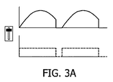
(調光された)整流電圧Urectは、マイクロコントローラ215のデジタル入力部218に交流結合される。第1の抵抗R211及び第2の抵抗R212は、デジタル入力部218への電流を制限する。整流電圧Urectの信号波形が高くなるとき、第1のキャパシタC213は、第1の抵抗R211及び第2の抵抗R212を通って立ち上がりエッジで充電される。例えば、第1のキャパシタC213が充電されている間、第1のダイオードD211は1ダイオード電圧降下分だけ電圧源Vccより上にデジタル入力部218をクランプする。信号波形がゼロでない限り、第1のキャパシタC213は充電されたままである。整流電圧Urectの信号波形の立ち下がりエッジで、第1のキャパシタC213は第2のキャパシタC214を通って放電され、デジタル入力部218は第2のダイオードD212によりグランドより1ダイオード電圧降下分低くクランプされる。後縁部調光器が用いられるとき、信号波形の立ち下がりエッジは波形のチョッピング部分の始まりに対応する。信号波形がゼロである限り、第1のキャパシタC213は放電されたままである。従って、デジタル入力部218の結果として生じる論理レベルデジタルパルスは、チョッピングされた整流電圧Urectの動きを密接にフォローし、これらの例が図3A乃至図3Cに示される。
The (dimmed) rectified voltage Urect is AC coupled to the
特に、図3A乃至図3Cは、典型的な実施例によるデジタル入力部218でのサンプル波形及び対応するデジタルパルスを示す。各図の一番上の波形は、チョッピングされた整流電圧Urectを示し、ここで、チョップの量は調光レベルを反映する。例えば、波形は、調光器の出力部に現れる全170V(又は、EUに対して340V)ピークの整流された正弦波の部分を示す。下の方形波は、マイクロコントローラ215のデジタル入力部218で見られる対応するデジタルパルスを示す。特に、各デジタルパルスの長さは、チョッピングされた波形に対応し、よって、調光器の内部スイッチが「オン」の時間量に等しい。デジタル入力部218を介してデジタルパルスを受信することにより、マイクロコントローラ215は、調光器が設定されたレベルを決定可能である。
In particular, FIGS. 3A-3C illustrate sample waveforms and corresponding digital pulses at the
図3Aは、調光器がその最も高い設定であるとき(波形の隣に示されるディマースライダの一番上の位置により示される)の整流電圧Urect及び対応するデジタルパルスのサンプル波形を示す。図3Bは、調光器が中程度の設定であるとき(波形の隣に示されるディマースライダの中間の位置により示される)の整流電圧Urect及び対応するデジタルパルスのサンプル波形を示す。図3Cは、調光器がその最も低い設定であるとき(波形の隣に示されるディマースライダの一番下の位置により示される)の整流電圧Urect及び対応するデジタルパルスのサンプル波形を示す。 FIG. 3A shows the sample waveform of the rectified voltage Urect and the corresponding digital pulse when the dimmer is at its highest setting (indicated by the top position of the dimmer slider shown next to the waveform). FIG. 3B shows a sample waveform of the rectified voltage Urect and the corresponding digital pulse when the dimmer is at a medium setting (indicated by the middle position of the dimmer slider shown next to the waveform). FIG. 3C shows a sample waveform of the rectified voltage Urect and the corresponding digital pulse when the dimmer is at its lowest setting (indicated by the bottom position of the dimmer slider shown next to the waveform).
図4は、典型的な実施例による調光器のディマーフェーズ角度を検出するプロセスを示す流れ図である。プロセスは、図2に示されるマイクロコントローラ215により実行されるファームウェア及び/又はソフトウェアにより、又は、更に一般的に、例えばプロセッサ又はコントローラにより、例えば図1に示されるフェーズ角度検出器110により実行される。
FIG. 4 is a flow diagram illustrating a process for detecting a dimmer phase angle of a dimmer according to an exemplary embodiment. The process is performed by firmware and / or software executed by the
図4のブロックS421において、入力信号のデジタルパルスの立ち上がりエッジ(例えば、図3A乃至図3Cの下の波形の立ち上がりエッジにより示される)は、例えば、第1のキャパシタC213の初期充電により検出される。マイクロコントローラ215のデジタル入力部218のサンプリングは、例えば、ブロックS422で始まる。示された実施例において、信号は、メイン半周期のちょうど下に等しい所定時間の間、デジタル的にサンプリングされる。信号がサンプリングされるたびに、サンプルが高レベル(例えば、デジタル「1」)又は低レベル(例えば、デジタル「0」)を持つかどうかがブロックS423で決定される。示された実施例において、サンプルがデジタル「1」であるかどうか決定するために、ブロックS423で比較がなされる。サンプルがデジタル「1」(ブロックS423:はい)であるとき、カウンタはブロックS424でインクリメントされ、サンプルがデジタル「1」でない(ブロックS423:いいえ)とき、小さな遅延がブロックS425で挿入される。サンプルがデジタル「1」又はデジタル「0」であると決定されるかどうかにかかわらず、(例えば、マイクロコントローラ215の)クロックサイクルの数が等しいように、遅延が挿入される。
In block S421 of FIG. 4, the rising edge of the digital pulse of the input signal (eg, indicated by the rising edge of the lower waveform in FIGS. 3A to 3C) is detected by, for example, initial charging of the first capacitor C213. . Sampling at the
ブロックS426において、全体のメイン半周期がサンプリングされたかどうかが決定される。メイン半周期が完了していないとき(ブロックS426:いいえ)、プロセスは、デジタル入力部218で再び信号をサンプリングするためにブロックS422へ戻る。メイン半周期が完了したとき(ブロックS426:はい)、サンプリングが止まり、ブロックS424で累算されたカウンタ値がブロックS427で現在のディマーフェーズ角度として識別され、カウンタはゼロへリセットされる。カウンタ値はメモリに保存され、この例は上述されている。マイクロコントローラ215は、その後、再びサンプリングを開始するため次の立ち上がりエッジを待つ。
In block S426, it is determined whether the entire main half cycle has been sampled. When the main half-cycle is not complete (block S426: No), the process returns to block S422 to sample the signal again at the
例えば、マイクロコントローラ215がメイン半周期の間、255個のサンプルをとると仮定される。調光レベル又はフェーズ角度が(例えば、図3Aに示されるように)その範囲の一番上近くのスライダにより設定されるとき、カウンタは図4のブロックS424で約255までインクリメントされる。調光レベルが(例えば、図3Cに示されるように)その範囲の下部近くのスライダにより設定されるとき、カウンタはブロックS424でわずか約10又は20までインクリメントされる。調光レベルが(例えば、図3Bに示されるように)その範囲の中央のどこかに設定されるとき、カウンタはブロックS424で約128までインクリメントされる。カウンタの値は、このように、マイクロコントローラ215に調光器が設定されたレベル又は調光器のフェーズ角度の正確な指標を与える。様々な実施例において、ディマーフェーズ角度は、例えば、カウンタ値の予め定められた機能を用いてマイクロコントローラ215により計算され、ここで、当該機能は、当業者に明らかなように、任意の特定の状況に対する固有の利点を提供するか又は様々な実行のアプリケーション特有の設計要件を満たすために変わってもよい。
For example, it is assumed that the
従って、調光器のフェーズ角度は、マイクロコントローラ(又は、他のプロセッサ若しくはコントローラ回路)のデジタル入力構造及び最小の受動部品を用いて電子的に検出される。実施例において、フェーズ角度検出は、交流結合回路、マイクロコントローラのダイオードクランプされたデジタル入力構造、及び調光設定レベルを決定するために実行される(例えば、ファームウェア、ソフトウェア及び/又はハードウェアにより実行される)アルゴリズムを使用して達成される。加えて、調光器の状況は、最小の部品数で測定され、マイクロコントローラのデジタル入力構造を利用している。 Thus, the phase angle of the dimmer is detected electronically using the digital input structure and minimal passive components of the microcontroller (or other processor or controller circuit). In an embodiment, phase angle detection is performed to determine the AC coupling circuit, the microcontroller diode-clamped digital input structure, and the dimming setting level (e.g., performed by firmware, software and / or hardware) To be achieved using an algorithm. In addition, the dimmer status is measured with a minimum number of parts and utilizes the digital input structure of the microcontroller.
位相角デジタル検出回路及び関連するアルゴリズムは、フェーズチョッピング調光器のフェーズ角度を知りたいと望まれる様々な状況で用いられる。例えば、フェーズチョッピング調光器への負荷として動作する電子トランスフォーマ(変成器)は、ディマーフェーズ角度を決定するために、この回路及び方法を使用する。ディマーフェーズ角度がわかると、半導体照明器具(例えばLED)に関する調光器との互換性及び調光のレベルが改善される。斯様な改善の例は、調光器設定を持つランプの色温度を制御し、調光器が原位置で処理できる最小の負荷を決定し、調光器が原位置で不規則に機能するときを決定し、光出力の最大及び最小範囲を増大させ、スライダ位置曲線に対するカスタムの調光ライトを作ることを含む。 The phase angle digital detection circuit and associated algorithms are used in various situations where it is desired to know the phase angle of the phase chopping dimmer. For example, an electronic transformer operating as a load to a phase chopping dimmer uses this circuit and method to determine the dimmer phase angle. Knowing the dimmer phase angle improves the dimmer compatibility and dimming level for solid state lighting fixtures (eg, LEDs). An example of such an improvement is to control the color temperature of a lamp with dimmer settings, determine the minimum load that the dimmer can handle in-situ, and the dimmer functions irregularly in-situ Including determining when, increasing the maximum and minimum range of light output, and creating a custom dimmable light for the slider position curve.
様々な実施例によるディマーフェーズ角度検出回路は、eW Blast Power Core、eW Burst Power Core、eW Cove MX Power Core及びeW PAR38等を含むPhilips Color Kinetics社から入手可能な様々なEssential White及び/又はeW製品で実行されている。更に、これは、様々な製品をよりフレンドリに調光させるための様々な製品に対する「スマートな」改善の構成要素として使用される。 Dimmer phase angle detection circuits according to various embodiments include various Essential White and / or various White products available from Philips Color Kinetics, including eW Burst Power Core, eW Burst Power Core, eW Cave MX Power Core, and eW PAR38. Running on. In addition, it is used as a “smart” improvement component for various products to make the various products more dimmable.
様々な実施例において、図2に示されるような典型的な検出回路のような検出回路は、同様に、フェーズチョッピング調光器の有無を決定するために用いられる。ディマーフェーズ角度と独立して発生する調光課題は、電力変換器が調光器の負荷として接続されているかどうかを最初に決定することにより、適切に処理される。これらの場合、調光器が存在するかに関する単純なバイナリの決定で充分であり、ディマーフェーズ角度に関する付加的情報が必要でないので、よって、調光器が存在するかどうかの単純なバイナリの検出より計算的に激しい上述のようなフェーズ角度検出を回避する。調光器の存在の決定は、例えば、LEDドライバを持つフェーズチョッピング調光器の互換性を改善するための幾つかの動作をするのに十分である。更に、バイナリの調光器存在アルゴリズムは、汎用入力メイン電圧を決定するような、より大きいアルゴリズムの一部として組み込まれてもよい。 In various embodiments, a detection circuit, such as the typical detection circuit as shown in FIG. 2, is similarly used to determine the presence or absence of a phase chopping dimmer. Dimming tasks that occur independently of the dimmer phase angle are handled appropriately by first determining whether the power converter is connected as a load on the dimmer. In these cases, a simple binary determination as to whether a dimmer is present is sufficient and no additional information about the dimmer phase angle is required, so a simple binary detection of whether a dimmer is present Avoid the more computationally intensive phase angle detection as described above. The determination of the presence of a dimmer is sufficient to do some operations to improve the compatibility of, for example, a phase chopping dimmer with an LED driver. In addition, a binary dimmer presence algorithm may be incorporated as part of a larger algorithm that determines the universal input main voltage.
図5は、典型的な実施例による調光器を持つ又は持たない照明器具のサンプル波形及び対応するデジタルパルスを示す。 FIG. 5 shows a sample waveform and corresponding digital pulse of a luminaire with or without a dimmer according to an exemplary embodiment.
図5を参照すると、波形の上のセットは、(隣接する調光器スイッチにより示される)接続された調光器を持って整流された入力メイン電圧及び対応する検出された論理レベルデジタルパルスを示す。波形の下のセットは、(隣接する調光器スイッチ全体が「X」により示される)接続される調光器のない整流された入力メイン電圧及び対応する検出された論理レベルデジタルパルスを示す。点線501は、調光器に対応する典型的な上位のレベル閾値を示す。上位のレベル閾値は、その最も高い設定で調光器の「オン」時間を経験的に測定し、製造業者データベースから「オン」時間を取り出す等を含む様々な手段により決定される。
Referring to FIG. 5, the upper set of waveforms shows the input main voltage rectified with the connected dimmer (indicated by the adjacent dimmer switch) and the corresponding detected logic level digital pulse. Show. The lower set of waveforms shows the rectified input main voltage and the corresponding detected logic level digital pulses without the connected dimmer (the entire adjacent dimmer switch is indicated by an “X”).
フェーズチョッピング調光器は、全整流メイン電圧正弦波を可能にせず、むしろ波形の上のセットに示されるように、その最も高い設定でさえ、各波形の区域をチョッピングする。比較すると、接続された調光器がない場合、波形の下のセットに示されるように、全整流メイン電圧正弦波は、通過可能である。例えば、フェーズ角度検出器210によって決定されるようなデジタルパルスが、上位のレベル閾値(波形の上のセットに示されるように)を越えて延在しない場合、調光器が存在すると決定される。デジタルパルスが上位のレベル閾値(波形の下のセットに示されるように)を越えて延在する場合、調光器が存在しないと決定される。 The phase chopping dimmer does not allow a full rectified main voltage sine wave, but rather chops each waveform area, even at its highest setting, as shown in the upper set of waveforms. By comparison, in the absence of a connected dimmer, the full rectified main voltage sine wave can pass as shown in the lower set of waveforms. For example, if a digital pulse as determined by phase angle detector 210 does not extend beyond the upper level threshold (as shown in the upper set of waveforms), it is determined that a dimmer is present. . If the digital pulse extends beyond the upper level threshold (as shown in the lower set of waveforms), it is determined that there is no dimmer.
図6は、典型的な実施例による調光器が存在するかどうかを決定するプロセスを示す流れ図である。プロセスは、例えば、図2のマイクロコントローラ215により実行されるファームウェア及び/又はソフトウェアにより実行される。
FIG. 6 is a flow diagram illustrating a process for determining whether a dimmer is present according to an exemplary embodiment. The process is performed, for example, by firmware and / or software executed by the
ブロックS621において、決定されたディマーフェーズ角度が取り出される。例えば、図4に示されたアルゴリズムに従って検出されるようなディマーフェーズ角度は、(例えば、ディマーフェーズ角度情報はブロックS247で格納された)メモリから取り出される。ディマーフェーズ角度(例えば、デジタルパルスの長さ)が上位のレベル閾値より小さいかどうかが、ブロックS622において決定される。ディマーフェーズ角度が上位のレベル閾値より小さくないとき(ブロックS622:いいえ)、プロセスはブロックS621へ戻り、決定されたディマーフェーズ角度が再び取り出されるので、ディマーフェーズ角度が監視され続ける。また、様々な実施例では、ディマー検出フラグは、調光器が存在しないことを示す「低い」に設定され、及び/又はプロセスは終了する。ディマーフェーズ角度が上位のレベル閾値より小さいと決定されるとき(ブロックS622:はい)、ディマー検出フラグは、例えば調光器の存在を示す、「高い」がブロックS623で設定される。もちろん、別の実施例では、本教示の要旨を逸脱しない範囲で、取り出されたフェーズ角度が、上位のレベル閾値より大きいか(小さいとは対照的に)どうかが決定されてもよい。 In block S621, the determined dimmer phase angle is retrieved. For example, the dimmer phase angle as detected according to the algorithm shown in FIG. 4 is retrieved from memory (eg, the dimmer phase angle information was stored in block S247). It is determined in block S622 whether the dimmer phase angle (eg, digital pulse length) is less than the upper level threshold. If the dimmer phase angle is not less than the upper level threshold (block S622: No), the process returns to block S621 and the dimmer phase angle continues to be monitored because the determined dimmer phase angle is again retrieved. Also, in various embodiments, the dimmer detection flag is set to “low” indicating that no dimmer is present and / or the process ends. When it is determined that the dimmer phase angle is smaller than the upper level threshold (block S622: Yes), the dimmer detection flag is set to “high” indicating the presence of a dimmer, for example, in block S623. Of course, in other embodiments, it may be determined whether the retrieved phase angle is greater (as opposed to smaller) than the upper level threshold without departing from the spirit of the present teachings.
従って、調光器の有無は、マイクロコントローラ(又は、他のプロセッサ若しくは処理回路)のデジタル入力構造及び最小の受動部品を用いて電子的に検出される。実施例において、調光器検出は、交流結合回路、マイクロコントローラダイオードクランプされたデジタル入力構造、及び調光器存在のバイナリ決定のために実行される(例えば、ファームウェア、ソフトウェア及び/又はハードウェアにより実行される)アルゴリズムを使用して達成される。上述のように、計算的により少ない強度及びタイミングに無関心なアルゴリズムが用いられてもよいが、例えば、半導体照明(例えば、LED)電力変換器がフェーズチョッピング調光器への負荷として接続されているかどうかを電子的に検出することは、図2に示される典型的な実施例の同じ部品を使用して達成されてもよい。 Thus, the presence or absence of a dimmer is electronically detected using the digital input structure and minimal passive components of the microcontroller (or other processor or processing circuit). In an embodiment, dimmer detection is performed for binary determination of dimmer presence (eg, by firmware, software and / or hardware), AC coupling circuit, microcontroller diode clamped digital input structure, and dimmer presence. This is accomplished using an algorithm that is executed. As noted above, algorithms that are computationally less concerned with less intensity and timing may be used, for example, whether a solid state lighting (eg, LED) power converter is connected as a load to the phase chopping dimmer The electronic detection of whether may be accomplished using the same parts of the exemplary embodiment shown in FIG.
調光器存在検出回路及び関連するアルゴリズムは、例えば、電子変成器がフェーズチョッピング調光器の負荷として接続されるかどうかを知っていることが望ましい様々な状況において用いられる。調光器の有無が決定されると、半導体照明器具(例えばLED)に関する調光器との互換性が改善される。斯様な改善の例は、調光器の全「オン」フェーズチョップによるハイエンド電力損失を補償し、調光器が存在しない場合、全ての不必要な機能を閉ざすことにより効率を増大し、調光器が存在する場合、調光器の最小の負荷要件を助けるためのブリーディング負荷に切り替わることを含む。 The dimmer presence detection circuit and associated algorithms are used, for example, in various situations where it is desirable to know whether an electronic transformer is connected as a load for a phase chopping dimmer. Once the presence or absence of the dimmer is determined, compatibility with the dimmer for semiconductor lighting fixtures (eg, LEDs) is improved. An example of such an improvement is to compensate for the high-end power loss due to the entire “on” phase chop of the dimmer, and in the absence of the dimmer, it increases efficiency by closing all unnecessary functions and dimming. If present, includes switching to a bleeding load to help the dimmer's minimum load requirements.
様々な実施例による調光器検出回路は、eW Blast Power Core、eW Burst Power Core、eW Cove MX Power Core及びeW PAR38等を含むPhilips Color Kinetics社から入手可能な様々なEssential White及び/又はeW製品で実行されている。更に、これは、様々な製品をよりフレンドリに調光させるための様々な製品に対する「スマートな」改善の構成要素として使用される。 Dimmer detection circuits according to various embodiments include various Essential White products and / or eW White products available from Philips Color Kinetics, including eW Blast Power Core, eW Burst Power Core, eW Cave MX Power Core, and eW PAR38. Running on. In addition, it is used as a “smart” improvement component for various products to make the various products more dimmable.
様々な実施例において、マイクロコントローラ215の機能は、ハードウェア、ファームウェア又はソフトウェアアーキテクチャの任意の組合せから構成される一つ以上の処理回路により実行され、様々な機能を実施可能にする実行可能なソフトウェア/ファームウェア実行コードを格納するためのそれ自身のメモリ(例えば、不揮発性メモリ)を含む。例えば、機能は、ASIC、FPGA等を使用して実行される。
In various embodiments, the functions of
出願人は、半導体照明器具のためのディマーフェーズ角度を検出できる回路に加えて、及び/又はフェーズチョッピング調光器が存在するかどうかにせよ、調光レベルが入力メイン電圧の決定をなすために十分高く設定されるとき、半導体照明器具に汎用電圧入力を供給するための入力メイン電圧を決定する回路を提供することが有益であることを認識し理解した。さもなければ、以前に決定された入力メイン電圧は、例えば、メモリから取り出される。 In addition to circuitry that can detect the dimmer phase angle for semiconductor luminaires and / or whether a phase chopping dimmer is present, Applicant will determine the dimming level to determine the input main voltage. It has been recognized and understood that it is beneficial to provide a circuit for determining an input main voltage for providing a general purpose voltage input to a solid state lighting fixture when set sufficiently high. Otherwise, the previously determined input main voltage is retrieved from the memory, for example.
図7は、様々な実施例による半導体照明器具用の典型的な照明システムを示す回路図である。図2の調光制御システム200と同様に、図7に示される調光制御システム700は、調光器(図示せず)に接続された整流回路705、ディマーフェーズ角度検出回路710(点線ボックス)、電力変換器720、入力波形サンプリング回路730(点線ボックス)及びLED負荷740を含む。マイクロコントローラ715は、ディマーフェーズ角度検出回路710及び入力波形サンプリング回路730両方に含まれる。
FIG. 7 is a circuit diagram illustrating an exemplary lighting system for a solid state lighting fixture according to various embodiments. Similar to the
示された構成において、整流回路705は、整流電圧ノードN2とグランドとの間に接続された4つのダイオードD701―D704を含む。整流電圧ノードN2は、(調光された)整流電圧Urectを受信し、整流回路705と並列に接続された入力フィルタリングキャパシタC715を介してグランドに接続される。
In the configuration shown,
ディマーフェーズ角度検出回路710は、制御ライン729に接続されたPWM出力部719のようなデジタル出力部を持つマイクロコントローラ715を含む。様々な実施例において、マイクロコントローラ715は例えばMicrochip Technology社から入手可能なPIC12F683であり、図2のマイクロコントローラ215に関して上述されたように、本教示の要旨を逸脱しない範囲で他のタイプのマイクロコントローラ又は他のプロセッサが含まれてもよい。示された実施例において、フェーズ角度検出回路710は、更に第1のキャパシタC213及び第2のキャパシタC214並びに第1の抵抗R211及び第2の抵抗R212を構成し実質的に同じ動作をする、第1のキャパシタC713及び第2のキャパシタC714並びに第1の抵抗R711及び第2の抵抗R712を含み、よって対応する説明は繰り返されない。従って、マイクロコントローラ715のデジタル入力部718での論理レベルデジタルパルスは、マイクロコントローラ715のデジタル入力部718に交流結合された、チョッピングされた整流電圧Urectの動きを密接にフォローする。
The dimmer phase
加えて、入力波形サンプリング回路730は、また、マイクロコントローラ715だけでなく、分割されたバージョンの整流電圧Urectを供給する第3の抵抗R731及び第4の抵抗R732を含む電圧分割器を含む。示された実施例において、第3の抵抗R731は整流電圧ノードN2と波形サンプリングノードN3との間に接続され、第4の抵抗R732は波形サンプリングノードN3とグランドとの間に接続される。実施例において、例えば、第3の抵抗R731は約1.5Mオームの値を持ち、第4の抵抗R732は約15kオームの値を持つ。しかしながら、第3の抵抗R731及び第4の抵抗R732それぞれの値は、当業者にとって明らかなように、任意の特定の状況に対する固有の利点を提供するか又は様々な実行のアプリケーション特有の設計要件を満たすために変わってもよい。
In addition, the input
入力波形サンプリング回路730は、分割されたバージョンの整流回路705からの入力整流電圧Urectを基本的に供給し、マイクロコントローラ715によりアナログ入力部717を介した入力波形の正確な表現を決定可能にする。マイクロコントローラ715は、チョッピングされていない入力メイン電圧、すなわち、調光器への入力部での電圧を決定するために、当該波形を使用する。上述のディマーフェーズ角度検出回路710の一部として、マイクロコントローラ715は、また、調光器のフェーズ角度(又は、調光レベル)に関する情報を受信する。
The input
上述のように、電力変換器720は、例えば参照により本願に組み込まれる米国特許第7,256,554号にて説明されたように、開ループ又はフィードフォワード形式で動作する。マイクロコントローラ715は、制御ライン729を介してPWM出力部719で電力制御信号出力を用いて電力変換器720の電力設定を調整可能である。様々な実施例において、電力変換器720は、例えばSTマイクロエレクトロニクス社から入手可能なL6562であり、本教示の要旨を逸脱しない範囲で他のタイプのマイクロコントローラ、電力変換器及び他のプロセッサが含まれてもよい。
As described above,
一般に、マイクロコントローラ715により実行されるソフトウェア及び/又はファームウェアアルゴリズムは、図8Aに示されるように、高いディマーフェーズ角度(チョッピングが少ない波形)で入力メイン電圧がより正確に決定できるという事実を利用し、これは、電力変換器720の電力設定をより正確に設定するために用いられる。しかしながら、図8Bに示されるように、低いディマーフェーズ角度(より重くチョッピングされた波形)での入力メイン電圧の決定は、計算的に重くなり、測定のためにほとんどの波形が利用できないので、ハイエンドマイクロコントローラ又は他のプロセッサ若しくはコントローラを必要とする。従って、様々な実施例によると、図9を参照して後述される例として、低いディマーフェーズ角度で斯様な重い分析を実施する代わりに、電力制御信号は、例えば、調光器が高いディマーフェーズ角度であるときに計算された入力メイン電圧の以前に決定され格納された値に基づいて設定されるか、又は図13を参照して後述される例として、より柔軟性のある(しかし、正確でない)分別(binning)アルゴリズムを使用して計算される。これは、ハイエンドマイクロコントローラ及び/又は比較的長い処理時間を組み込む必要性を回避する。
In general, the software and / or firmware algorithm executed by the
あるディマーフェーズ角度を超えると入力波形及び入力メイン電圧のより正確な決定が発生する当該ディマーフェーズ角度は、決定閾値と呼ばれる。様々な実施例において、決定閾値は、マイクロコントローラ715が入力メイン電圧の正確な決定をするために充分なサンプルを収集可能である調光器の予め定められたフェーズ角度である。従って、決定閾値は、例えば、マイクロコントローラ715の速度及びチョッピングされた波形から入力メイン電圧を決定するために用いられるアルゴリズムの効果のような様々な要因に依存して変化する。従って、マイクロコントローラ715のコストと、制御ライン729を介して電力変換器720へマイクロコントローラ715により供給される電力信号の正確さとは、トレードオフである。
The dimmer phase angle at which a more accurate determination of the input waveform and input main voltage occurs when a certain dimmer phase angle is exceeded is called the decision threshold. In various embodiments, the decision threshold is a dimmer predetermined phase angle that allows the
図8Aは、例えば、図14及び図15それぞれを参照して後述されるピーク及び傾斜検出アルゴリズムを用いて、図7に示される入力波形サンプリング回路730及びアナログ入力部717を介して、正確な入力電圧測定がマイクロコントローラ715によりなされる典型的な実施例による決定閾値を上回るフェーズ角度を持つ調光器のサンプル波形を示す。図8Bは、決定閾値より低いフェーズ角度を持つ調光器のサンプル波形を示し、典型的な実施例によると、例えば、ディマーフェーズ角度が決定閾値を超えるときに計算された以前に決定された入力電圧及び対応する最後の最良の電力設定が、電力変換器の電力を設定するために用いられる。代わりに、以前に決定された入力電圧が利用できないとき、入力電圧及び対応する電力設定は、図13を参照して後述される例の分別のような計算より幾らか不正確な代わりの方法を用いて決定される。
FIG. 8A shows an accurate input via the input
図9は、典型的な実施例による検出されたディマーフェーズ角度に基づいて入力メイン電圧及び対応する電力設定を決定するプロセスを示す流れ図である。 FIG. 9 is a flow diagram illustrating a process for determining an input main voltage and a corresponding power setting based on a detected dimmer phase angle according to an exemplary embodiment.
図9を参照して、示された実施例では、プロセスが半導体照明器具の最初のパワーアップに従って実行されているかどうかがブロックS910において最初に決定され、これは、最初の電力が半導体照明器具に付与されるときに発生する。最初のパワーアップでないとき(ブロックS910:いいえ)、ブロックS920において、以前に決定された入力メイン電圧値が、EEPROMのようなメモリから取り出される。代わりに、メモリは、RAM、ROM、PROM、EPROM、USBドライブ、フロッピー(登録商標)ディスク、コンパクトディスク、光ディスク、磁気テープ等のような任意のタイプの揮発性又は不揮発性コンピュータメモリを含む。以前に決定された入力メイン電圧値は、例えば、事前に取り付けられたルックアップテーブル又は関連の他の手段を使用して、電力変換器720の関連する電力設定と相関される。関連する電力設定はマイクロコントローラ715から電力制御信号出力部を介して電力変換器720に付与されるので、現在の入力メイン電圧が決定されている間、半導体照明器具は通常動作する。
Referring to FIG. 9, in the illustrated embodiment, it is first determined in block S910 whether the process is being performed according to the first power up of the solid state lighting fixture, which is the first power to the solid state lighting fixture. Occurs when granted. When it is not the first power-up (block S910: No), in block S920, the previously determined input main voltage value is retrieved from a memory such as an EEPROM. Instead, the memory includes any type of volatile or non-volatile computer memory such as RAM, ROM, PROM, EPROM, USB drive, floppy disk, compact disk, optical disk, magnetic tape, and the like. The previously determined input main voltage value is correlated with the associated power setting of
ディマーフェーズ角度は、ブロックS921において検出される。ディマーフェーズ角度は、例えば、上述されたように図4に示されるディマーフェーズ角度検出プロセスに従って得られる。ブロックS922において、ディマーフェーズ角度が決定閾値より低いかどうかが決定される。ディマーフェーズ角度が決定閾値より低いとき(ブロックS922:はい)、以前に決定された入力メイン電圧及び最後の最良の電力設定と呼ばれる関連する電力設定が、ブロックS924において現在の電力設定として使われる。実施例において、最後の最良の電力設定は、ブロックS920で取り出された入力メイン電圧に基づいて決定された電力設定であり、ディマーフェーズ角度が決定閾値より低いときブロックS924において単に変えられないままである。 The dimmer phase angle is detected in block S921. The dimmer phase angle is obtained, for example, according to the dimmer phase angle detection process shown in FIG. 4 as described above. In block S922, it is determined whether the dimmer phase angle is below a decision threshold. When the dimmer phase angle is below the decision threshold (block S922: yes), the previously determined input main voltage and the associated power setting called the last best power setting is used as the current power setting in block S924. In an embodiment, the last best power setting is a power setting determined based on the input main voltage retrieved at block S920, and remains simply unchanged at block S924 when the dimmer phase angle is below the decision threshold. is there.
ディマーフェーズ角度が決定閾値より低くないとき(ブロックS922:いいえ)、新しい入力メイン電圧及び対応する電力設定がブロックS926において決定される。実施例において、入力波形サンプリング回路730及びマイクロコントローラ715のアナログ入力波形分割器が、正確な入力メイン電圧及び電力設定を決定するために、例えば図14及び図15を参照して後述されるピーク及び傾斜検出アルゴリズムで使用される。例えば、マイクロコントローラ715は、後述される図10のコントローラ1020と実質的に同じように実行され、よって、(図10のA/D1022のような)AD変換器からDC電圧信号のデジタル値を受信し、当該デジタル値は、第3の抵抗R731及び第4の抵抗R732を含む電圧分割器から分割されたバージョンの整流電圧Urectに対応する。
When the dimmer phase angle is not below the decision threshold (block S922: No), a new input main voltage and corresponding power setting is determined in block S926. In an embodiment, the input
ディマーフェーズ角度が上記決定閾値より上であることが知られているので、図13を参照して後述されるように、複数の予め決定された入力電圧及び電力設定のうちの1つに制限(すなわち、分別)することと対照的に、正確な入力メイン電圧が、連続して決定される。言い換えると、図14及び図15のピーク及び傾斜検出方法は、入力メイン電圧の値を特に決定し、よって正確な電力設定を決定するために使用できる。前述のように、入力メイン電圧の決定された値は、例えば、事前に取り付けられたルックアップテーブル又は関連の他の手段を使用して、電力設定と相関される。 Since the dimmer phase angle is known to be above the decision threshold, it is limited to one of a plurality of predetermined input voltage and power settings (as will be described later with reference to FIG. 13). In contrast to sorting, the correct input main voltage is determined continuously. In other words, the peak and slope detection methods of FIGS. 14 and 15 can be used to specifically determine the value of the input main voltage and thus determine the exact power setting. As described above, the determined value of the input main voltage is correlated with the power setting using, for example, a pre-installed look-up table or other related means.
ブロックS910を再び参照して、最初のパワーアップが決定されるとき(ブロックS910:はい)、メモリからロードする、以前に決定された入力メイン電圧電力設定はない。よって、プロセスは、ブロックS921に関して上述されたように、ディマーフェーズ角度が検出されるブロックS911へ進む。ブロックS912において、ディマーフェーズ角度が決定閾値より低いかどうかが決定される。ディマーフェーズ角度が決定閾値より低くないとき(ブロックS912:いいえ)、新しい入力メイン電圧及び対応する電力設定が、上述のように、ブロックS926において決定される。 Referring back to block S910, when the first power up is determined (block S910: yes), there is no previously determined input main voltage power setting to load from memory. Thus, the process proceeds to block S911 where the dimmer phase angle is detected as described above with respect to block S921. In block S912, it is determined whether the dimmer phase angle is below a decision threshold. When the dimmer phase angle is not below the decision threshold (block S912: No), a new input main voltage and corresponding power setting is determined at block S926, as described above.
しかしながら、ディマー設定が決定閾値より低いとき(ブロックS912:はい)、取り出されるべき以前に決定された入力メイン電圧がないので、分別検出アルゴリズムが、複数の分別、例えば、120V、230V又は277Vの1つの入力メイン電圧を配置するようにブロックS914において実行される。分別検出アルゴリズムの例は、図13を参照して以下に説明される。その後、分別された電圧に対応する電力設定は、例えば、波形のより正確な決定、よって入力メイン電圧及び電力設定が分別なしになされる図9の方法の後続のパフォーマンスに従って、ディマーフェーズ角度が決定閾値を上回って動いたと決定されるまで、電力変換器720により用いられる。様々な実施例において、ブロックS914は、本教示の要旨を逸脱しない範囲で、入力電圧を推定するためブロックS926の入力電圧決定アルゴリズムより少ないチョッピングされた波形を必要とする(よって、より低いディマーフェーズ角度で機能する)分別以外のアルゴリズムを含んでもよい。
However, when the dimmer setting is lower than the decision threshold (block S912: yes), there is no previously determined input main voltage to be retrieved, so the classification detection algorithm can be used for multiple classifications, eg, 120V, 230V or
フェーズ角度及び決定閾値検出回路並びに関連するアルゴリズムは、電力変換器の電力設定を設定することが望ましい様々な状況において用いられる。様々な実施例によると、負荷LED電力は、例えば、ディマーフェーズ角度が決定閾値を超えるとき、比較的低い電力/低コストプロセッサを使用して、入力メイン電圧の連続的な範囲にわたって調整される。例えば、LED負荷に対する実際の電力は、マイクロコントローラが電力変換器へ送信する信号及びRMS入力電圧により決定される。 Phase angle and decision threshold detection circuits and associated algorithms are used in various situations where it is desirable to set the power settings of a power converter. According to various embodiments, the load LED power is adjusted over a continuous range of input main voltage using, for example, a relatively low power / low cost processor when the dimmer phase angle exceeds a decision threshold. For example, the actual power for the LED load is determined by the signal that the microcontroller sends to the power converter and the RMS input voltage.
分別プロセスは、例えば、マイクロコントローラから電力変換器へ送信された電力制御信号を、限定された数のあり得る値(例えば、入力メイン電圧120V、230V又は277Vに応じて3つの値)へ設定する。LEDへの実際の電力がRMS入力電圧及びマイクロコントローラ信号により決定されるので、RMS入力電圧が例えば179V又は208Vであるとき、正確な電力がLEDに供給されない。例えば、分別実行は、100V(一般に、日本で使われる)と120V(一般に北アメリカで使われる)と間の違いを決定しない。分別実行はマイクロコントローラからの電力制御信号を120Vに対して適当な値に設定するが、結果として、100Vで動くとき、RMS入力電圧は、より低くなり、よって、LEDに供給される電力及び光出力は正しくない。同様に、欧州において、入力メイン電圧は220V又は240Vであり、これは同じ課題を生じる。例えば、図2のデジタルフェーズ角度検出回路の使用は、ディマー設定が十分に高いとき、少なくともこれらの状況で決定されるべき正確な入力メイン電圧(及び対応する電力設定)を可能にする。 The fractionation process, for example, sets the power control signal transmitted from the microcontroller to the power converter to a limited number of possible values (eg, three values depending on the input main voltage 120V, 230V or 277V). . Since the actual power to the LED is determined by the RMS input voltage and the microcontroller signal, when the RMS input voltage is, for example, 179V or 208V, the correct power is not supplied to the LED. For example, fractional execution does not determine the difference between 100V (typically used in Japan) and 120V (commonly used in North America). The fractional run sets the power control signal from the microcontroller to an appropriate value for 120V, but as a result, when operating at 100V, the RMS input voltage is lower, thus the power and light supplied to the LEDs. The output is incorrect. Similarly, in Europe, the input main voltage is 220V or 240V, which causes the same problem. For example, the use of the digital phase angle detection circuit of FIG. 2 allows for an accurate input main voltage (and corresponding power setting) to be determined at least in these situations when the dimmer setting is sufficiently high.
また、上述のように、重くチョッピングされた正弦波の入力メイン電圧を決定することは、困難である。よって、ディマーフェーズ角度が非常に低い(例えば、図8Bに示されるように)とき、チョッピングされた区域が一部にある全正弦波を決定することは高コストで計算的に重い。様々な実施例によると、これは、例えば、マイクロコントローラ715の処理パワー又は負荷を大幅に増大する必要なしに、正確な決定がなされる、調光器が決定閾値を超えるときだけ、入力メイン電圧を決定することにより回避できる。
Also, as described above, it is difficult to determine the input main voltage of a heavily chopped sine wave. Thus, when the dimmer phase angle is very low (eg, as shown in FIG. 8B), determining a full sine wave with some chopped areas is expensive and computationally heavy. According to various embodiments, this is done only when the dimmer exceeds the decision threshold, for example, when an accurate decision is made without having to significantly increase the processing power or load of the
図10は、典型的な実施例による半導体照明器具及び入力電圧コントローラを含む照明システムを示すブロック図である。図10を参照すると、入力電圧コントローラ1010は、電圧分割器1015、A/Dコンバータ1022、コントローラ1020及び遷移モード力率補正(PFC)コントローラ1030を含む。
FIG. 10 is a block diagram illustrating a lighting system including a solid state lighting fixture and an input voltage controller according to an exemplary embodiment. Referring to FIG. 10, the
電圧分割器1015は、電力源から整流電圧を受信する。一般に、整流電圧は、例えば、約90VACと約277VACとの間の電圧値を持つ入力メイン又はACライン電圧信号及び対応する波形である。入力メイン電圧信号は、半導体照明器具1040を給電するために用いられる。電圧分割器1015は、分割されたバージョンの整流入力メイン電圧信号に対応する信号を供給する。電圧信号は、アナログの入力電圧信号としてA/Dコンバータ1022へ供給される。
The
示された実施例において、電圧分割器1015は、コントローラ1020の入力部に接続されるノードN11と整流入力メイン電圧源との間に直列に接続される第1の抵抗1011及び第2の抵抗1012を含む。電圧分割器1015は、更に、ノードN11とグランドとの間に接続された第3の抵抗1013を含む。実施例では、第1の抵抗1011及び第2の抵抗1012各々は、約750kオームの抵抗を持ち、第3の抵抗113は約13kオームの抵抗を持つ。他の実施例では、第1乃至第3の抵抗1011―1013の抵抗値及び/又は電圧分割器1015の構成は、当業者にとって明らかなように、任意の特定の状況に対する固有の利点を提供するか又は様々な実行のアプリケーション特有の設計要件を満たすために変わってもよいことは理解される。
In the illustrated embodiment, the
A/Dコンバータ1022は、電圧分割器1015からアナログ入力電圧信号を受信し、アナログの入力電圧信号を整流入力メイン電圧の波形を示すデジタル値へ変換する。コントローラ1020は、A/Dコンバータ1022からデジタル値を受信し、デジタル値に基づいて入力メイン電圧の電圧レベルを決定する。コントローラ1020は、入力メイン電圧の決定された電圧レベルに基づいて制御信号を調整し、半導体照明器具1040を制御するために、PFCコントローラ1030へ制御信号を出力する。例えば、制御信号に基づいて、PFCコントローラ1030は、後述されるように、入力メイン電圧(例えば、120VAC、230VAC又は277VAC)の任意の検出値に対する30Wの定常状態で半導体照明器具1040を動作させるために、電力変調制御信号を出力する。
The A /
コントローラ1020は、本教示の要旨を逸脱しない範囲で、上述のように、ハードウェア、ファームウェア又はソフトウェアアーキテクチャの組合せから構成される。また、コントローラ1020は、電圧コントローラ1010の様々な機能を実施可能にする実行可能なソフトウェア/ファームウェア実行コードを格納するためのそれ自身のメモリ(例えば、不揮発性メモリ)を含む。例えば、様々な実施例では、コントローラ1020は、マイクロプロセッサ、ASIC、FPGA、Microchip Technology社から入手可能なPIC12F683マイクロコントローラのようなマイクロコントローラ等として実行される。同様に、PFCコントローラ1030は、本教示の要旨を逸脱しない範囲で、ハードウェア、ファームウェア又はソフトウェアアーキテクチャの任意の組合せから構成される。例えば、様々な実施例では、PFCコントローラ1030は、マイクロプロセッサ、ASIC、FPGA、STマイクロエレクトロニクス社から入手可能なL6562PFCコントローラのようなマイクロコントローラ等として実行される。加えて、別々に示されているが、A/Dコンバータ1022及び/又はPFCコントローラ1030並びに関連する機能が、様々な実施例において、コントローラ1020内に組み込まれてもよいことは理解される。更に、様々な実施例では、コントローラ1020及びPFCコントローラ1030は、本教示の要旨を逸脱しない範囲で、例えば図7の電力コントローラ720及びマイクロコントローラ715により実行される。
The
図11は、典型的な実施例によるコントローラ1020のブロック図である。図11を参照すると、コントローラ1020は、プロセッサ1024、ROM1026、RAM1027及びPWM信号発生器1028を含む。
FIG. 11 is a block diagram of a
上述のように、A/Dコンバータ1022は、電圧分割器1015から入力信号を受信し、入力信号を整流入力メイン電圧の波形を示すデジタル値へ変換する。デジタル値は、処理のためプロセッサ1024により受信され、また、例えば、バス1021を介してROM1026及び/又はRAM1027に格納される。プロセッサ1024は、電圧コントローラ1010の様々な機能を実施可能にする実行可能なソフトウェア/ファームウェア実行コードを格納するためのそれ自身のメモリ(例えば、不揮発性メモリ)を含む。代わりに、実行コードは、ROM1026及び/又はRAM1027内の指定されたメモリ位置に格納される。ROM1026は、PROM、EPROM、EEPROM等のような有形のコンピュータ可読の記憶メディアの任意の数、タイプ及び組合せを含む。更に、ROM1026及び/又はRAM1027は、例えば、プロセッサ1024により以前の入力メイン電圧計算の結果及び統計的データを格納する。
As described above, the A /
PWM信号発生器1028は、プロセッサ1024からの命令又は制御信号に応じて、制御信号としてPWM信号を生成し出力する。とりわけ、示された実施例では、PWM信号発生器1028は、プロセッサ1024により決定される入力メイン電圧の値に依存して、PWM制御信号のパルス幅を変化させる。例えば、PWM信号発生器1028は、入力メイン電圧のより高い値に応じて、より短いパルス幅を持つPWM制御信号を生成する。PWM制御信号はコントローラ1020からPFCコントローラ1030へ出力され、PFCコントローラ1030は、PWM制御信号のパルス幅に関連する半導体照明器具140の電力変調を制御する。例えば、PFCコントローラ1030は、より大きいパルス幅に応じて半導体照明器具1040への電流を増大するように構成され、よって、低い電圧値(例えば、120VAC)に対する一定電力を維持する。同様に、PFCコントローラ1030は、より短いパルス幅に応じて、半導体照明器具1040への電流を減少するように構成され、よって、高い電圧値(例えば、277VAC)に対する一定電力を維持する。
The
例えば実施例において、PFCコントローラ1030は、その装置上に専用の電流設定ピンを持つ。電流設定ピン上に電圧基準を設定することにより、PFCコントローラ1030は、電流設定ピン上に見られる電圧基準に関する電力量を半導体照明器具1040へ送達する。(入力電圧波形に依存してパルス幅を変えながら)コントローラ1020から出力されたPWM制御信号出力は、PFCコントローラ1030のフィルタ回路(図示せず)を通過して、効果的にPFCコントローラ1030の電流設定ピン上の電圧基準を変える。これは、半導体照明器具1040のLEDアレイ1045のLEDを通過する全体の電力の変化を可能にする。もちろん、他のタイプの制御信号、及び半導体照明器具1040を制御する方法は、本教示の範囲内に組み込まれる。
For example, in an embodiment, the PFC controller 1030 has a dedicated current setting pin on the device. By setting the voltage reference on the current setting pin, the PFC controller 1030 delivers the amount of power related to the voltage reference found on the current setting pin to the solid
再び図10を参照すると、半導体照明器具1040は、例えば、Philips Color Kinetics社から入手可能な照明器具、Essential Whiteである。半導体照明器具1040は、典型的なLEDアレイ1045のような光源又は照明源及びスイッチ1041を含む。スイッチ1041は、PFCコントローラ1030から受信された電力変調制御信号に応じてLEDアレイ1045への電力のオン/オフを切り替え、これは同時に定常状態電流を変える。例えば、「オン」時間の量は、LEDアレイ1045のLEDを通る電流量を決定する。このようにLEDアレイ1045への電力の切り替えタイミング又はサイクルは、入力メイン電圧の様々な値に対して調整される。例えば、より高い入力メイン電圧(例えば、277VAC)は、定常状態電力(例えば、30W)をLEDアレイ1045へ供給するために、低い入力メイン電圧(例えば、120VAC)より短い「オン」間隔(結果的により少ない電流になる)を要求する。
Referring again to FIG. 10, the
図12は、典型的な実施例による半導体照明器具の電力を制御するプロセスを示す流れ図である。図12に示される様々なステップ及び/又はオペレーションは、例えば、図10及び図11を参照して上述されたA/Dコンバータ1022及びコントローラ1020により実行されてもよい。
FIG. 12 is a flow diagram illustrating a process for controlling the power of a solid state lighting fixture according to an exemplary embodiment. The various steps and / or operations shown in FIG. 12 may be performed by, for example, the A /
ブロックS1210において、整流ACライン電圧又は入力メイン電圧信号は、半導体照明器具を給電するために受信される。入力メイン電圧信号の大きさ又は値は、既知ではなく、120VAC、230VAC又は277VACのような様々な利用可能な入力メイン電圧の任意の一つである。ブロックS1212において、入力メイン電圧信号は、例えば、入力メイン電圧信号の波形に対応する分割された信号を供給する電圧分割器1015により、分割された信号へ変換される。分割された信号は、入力メイン電圧信号の波形を表わすデジタル値を供給するためにブロックS1214において、例えば、A/Dコンバータ1022によりアナログ信号からデジタル信号へ変換される。
In block S1210, a rectified AC line voltage or input main voltage signal is received to power a solid state lighting fixture. The magnitude or value of the input main voltage signal is not known and is any one of a variety of available input main voltages, such as 120 VAC, 230 VAC, or 277 VAC. In block S1212, the input main voltage signal is converted into a divided signal by, for example, a
オペレーションS1216において、入力メイン電圧信号の大きさ又は値は、図13乃至図15を参照して以下に更に詳細に説明されるデジタル値を使用して、例えばコントローラ1020及び/又はプロセッサ1024により決定される。一般に、ピーク検出アルゴリズムは、入力メイン電圧が高い値か又は中間の値(例えば、277VAC又は220―240VAC)を持つかどうかを決定するために実行される。しかしながら、ピーク検出アルゴリズム単独では、例えば、入力メイン電圧が低い値(例えば、120VAC)を持つとき、又は入力メイン電圧信号が調光された中間の値(例えば、230VAC)を持つとき、入力メイン電圧の値を検出できない。ピーク検出アルゴリズムが入力メイン電圧の値を検出できないとき、入力メイン電圧信号波形の立ち上がりエッジの傾斜が低い値又は中間の値に対応するかどうかを決定するための傾斜検出アルゴリズムが実施される。
In operation S1216, the magnitude or value of the input main voltage signal is determined, for example, by the
入力メイン電圧の値が決定された後、ブロックS1218で、決定された値に基づいて、制御信号が生成され、例えばPFCコントローラ1030へ出力される。制御信号に基づいて、半導体照明器具の電力変調は、入力メイン電圧値を考慮するように調整される。 After the value of the input main voltage is determined, a control signal is generated based on the determined value in block S1218 and output to the PFC controller 1030, for example. Based on the control signal, the power modulation of the solid state lighting fixture is adjusted to take into account the input main voltage value.
図13は、典型的な実施例による入力メイン電圧信号の値を決定するプロセスを示す流れ図である。より詳しくは、図13は、入力メイン電圧(又は、ACライン電圧)の値が複数の予め定められた電圧値(例えば、低い、中間、又は高い)の1つと関連している典型的な実施例を示す。プロセスは、入力メイン電圧が予め定められた電圧値の1つに対応する「ビン」に置かれるので、「分別」と呼ばれる。 FIG. 13 is a flow diagram illustrating a process for determining the value of the input main voltage signal according to an exemplary embodiment. More particularly, FIG. 13 illustrates an exemplary implementation in which the value of the input main voltage (or AC line voltage) is associated with one of a plurality of predetermined voltage values (eg, low, medium, or high). An example is shown. The process is called “fractionation” because the input main voltage is placed in a “bin” corresponding to one of the predetermined voltage values.
様々な実施例において、フェーズチョッピング調光器により生じるチョッピングされた正弦波が入力メイン電圧の正確な値を決定可能にするのに十分なときはいつでも、入力メイン電圧の正確な値は、例えば、図13のブロックS1320及びS1350に示されるピーク及び傾斜検出プロセスに基づいて決定される。例えば、図7乃至図9を参照して上述されたように、ディマーフェーズ角度が決定閾値を超えるとき(例えば、図8Aに示されるように)、入力メイン電圧の正確な値が比較的ほとんど処理パワーなしに計算される。 In various embodiments, whenever the chopped sine wave produced by the phase chopping dimmer is sufficient to allow the exact value of the input main voltage to be determined, the exact value of the input main voltage is, for example, It is determined based on the peak and slope detection process shown in blocks S1320 and S1350 of FIG. For example, as described above with reference to FIGS. 7-9, when the dimmer phase angle exceeds the decision threshold (eg, as shown in FIG. 8A), the exact value of the input main voltage is relatively little processed. Calculated without power.
図13を参照すると、プロセスは、例えばブロックS1312及びS1314により示されるように、最初に初期化される。初期化は、完全に省略されるか、又は本教示の要旨を逸脱しない範囲で、代替の実施例で入力メイン電圧の値を決定するプロセス内の他の時に実施されてもよいが、実施例において、初期化は、半導体照明器具をパワーアップする際にだけ実施される。利用できるとき、以前に決定された入力メイン電圧値がブロックS1312でメモリから取り出され、例えば、コントローラ1020により出力される制御信号は、ブロックS1314で以前に決定された入力メイン電圧値に基づいて最初に設定される。例えば、制御信号がPWM制御信号である場合、PWMパルス幅又はデューティサイクルは、以前に決定された入力メイン電圧値に従って先ず設定される。例えば、半導体照明器具がオンされるたびに、入力メイン電圧の値が決定され、例えば、ROM1026に格納される。従って、入力メイン電圧の現在の値が決定されている間、半導体照明器具は入力メイン電圧の以前に決定された値で動作される。これは、決定プロセスの間、フリッカ又は他の悪影響を防止する。
Referring to FIG. 13, the process is first initialized, for example, as indicated by blocks S1312 and S1314. Initialization may be omitted at any other time within the process of determining the value of the input main voltage in alternative embodiments, as long as it is omitted entirely or does not depart from the spirit of the present teachings. The initialization is performed only when powering up the solid state lighting fixture. When available, the previously determined input main voltage value is retrieved from the memory at block S1312, for example, the control signal output by the
オペレーションS1320において、ピーク検出アルゴリズムは、例えば、A/Dコンバータ122により供給されるデジタル値に基づいて、入力メイン電圧信号のピーク及び周波数を検出するために実施される。オペレーションS1320のピーク検出アルゴリズムは、典型的な実施例による入力メイン電圧信号の信号ピーク及び周波数を決定するプロセスを示す流れ図である図14を参照して詳述される。 In operation S1320, the peak detection algorithm is implemented to detect the peak and frequency of the input main voltage signal based on, for example, a digital value supplied by the A / D converter 122. The peak detection algorithm of operation S1320 is described in detail with reference to FIG. 14, which is a flow diagram illustrating the process of determining the signal peak and frequency of the input main voltage signal according to an exemplary embodiment.
図14を参照すると、(例えば、図12のブロックS1214からの)DC電圧信号のデジタル値は、入力メイン電圧信号波形のピークに対応する最大デジタル値を識別し格納するために、及び/又は入力メイン電圧信号の周波数を識別するために、予め定められた数のサイクル(例えば、20サイクル)の間、又は、所定の期間(例えば、150mS)の間、読み取られる。例えば、プロセッサ1024は、A/Dコンバータ1022からDC電圧信号の多くのデジタル値をサンプリングする。最大デジタル値を識別するために、分割された信号(分割されたバージョンの整流入力メイン電圧に対応する)のデジタル値は、ブロックS1421において読み取られ、ブロックS1422において最大値と比較される。最大値は、予め定められた閾値、又は前に読み取られたデジタル値の中から最大値であると前もって決定され格納されたデジタル値である。
Referring to FIG. 14, the digital value of the DC voltage signal (eg, from block S1214 of FIG. 12) is used to identify and store the maximum digital value corresponding to the peak of the input main voltage signal waveform and / or input. To identify the frequency of the main voltage signal, it is read for a predetermined number of cycles (eg, 20 cycles) or for a predetermined period of time (eg, 150 mS). For example, the
読み取られたデジタル値が最大値より大きいとき(ブロックS1422:はい)、読み取られたデジタル値は、その後読み取られたデジタル値との比較に使われるため、ブロックS1423において新しい最大値として格納される。読み取られたデジタル値が最大値より大きくないとき(ブロックS1422:いいえ)、ブロックS1423は、スキップされる。付加的なサイクル(又は時間)がデジタル値を読み取るために残っているかどうかが、ブロックS1424において決定される。例えば、サイクル数又は経過時間は、予め定められた閾値又はデジタル値を読み取るための所定の時間とそれぞれ比較される。付加的なサイクル又は時間があるとき(ブロックS1424:はい)、ブロックS1421乃至S1423は、繰り返される。付加的なサイクル又はデジタル値を読み取るための時間がないとき(ブロックS1424:いいえ)、サンプリングされたデジタル値の中の現在の最大値が、波形のピークの値とみなされる。 When the read digital value is greater than the maximum value (block S1422: Yes), the read digital value is stored in block S1423 as a new maximum value for subsequent comparison with the read digital value. When the read digital value is not larger than the maximum value (block S1422: No), block S1423 is skipped. Whether additional cycles (or times) remain to read the digital value is determined in block S1424. For example, the number of cycles or elapsed time is compared to a predetermined threshold or a predetermined time for reading a digital value, respectively. When there are additional cycles or times (block S1424: yes), blocks S1421 to S1423 are repeated. When there is no additional cycle or time to read the digital value (block S1424: No), the current maximum value among the sampled digital values is considered the value of the waveform peak.
入力メイン電圧の波形の周波数は、例えば、ゼロクロス間又は隣接するピーク値間のタイミングを比較することにより、ブロックS1425において計算される。例えば、入力メイン電圧が通常半導体照明器具取付けの地理的な位置により表わされている50Hz又は60HzであるかがブロックS1425において決定される。波形の周波数は、後述されるように、図13のオペレーションS1350において計算される波形の傾斜に直接影響するので、波形の周波数が決定される。実施例において、波形の周波数は、サイクル期間にわたって波形の波上のポイント(例えば、波のピーク又は開始点)をサンプリングし、隣接する波間の時間量を計算することにより決定される。 The frequency of the waveform of the input main voltage is calculated in block S1425, for example, by comparing timing between zero crossings or adjacent peak values. For example, it is determined in block S1425 whether the input main voltage is typically 50 Hz or 60 Hz represented by the geographical location of the solid state lighting fixture installation. As will be described later, the frequency of the waveform directly affects the slope of the waveform calculated in operation S1350 of FIG. 13, and therefore the waveform frequency is determined. In an embodiment, the frequency of the waveform is determined by sampling a point on the waveform wave (eg, a wave peak or starting point) over a cycle period and calculating the amount of time between adjacent waves.
図14のブロックS1425において周波数を決定した後に、プロセスは図13に戻る。図13のブロックS1332乃至S1335において、入力メイン電圧信号の値が、対応する波形の傾斜を決定する必要なく決定できるかどうかが決定される。特に、ブロックS1332において、波形のピーク値は、入力メイン電圧信号の値が最大電圧値(例えば、277VAC)であるかどうかを決定するために予め定められた第1の閾値と比較される。ピーク値が第1の閾値より大きいとき(ブロックS1332:はい)、ブロックS1333において入力メイン電圧信号の値が最大電圧値であることが決定される。 After determining the frequency in block S1425 of FIG. 14, the process returns to FIG. In blocks S1332 to S1335 of FIG. 13, it is determined whether the value of the input main voltage signal can be determined without having to determine the slope of the corresponding waveform. In particular, in block S1332, the peak value of the waveform is compared to a predetermined first threshold value to determine whether the value of the input main voltage signal is a maximum voltage value (eg, 277 VAC). When the peak value is greater than the first threshold (block S1332: yes), it is determined in block S1333 that the value of the input main voltage signal is the maximum voltage value.
ピークの値が第1の閾値より大きくないとき(ブロックS1332:いいえ)、プロセスは、入力メイン電圧信号の値が中間の電圧値(例えば、230VAC)であるか、又は可能性がある中間の電圧値(例えば、220VAC乃至240VAC)の範囲であるかどうかを決定するために波形のピーク値が予め定められた第2の閾値と比較されるS1334へと進む。ピーク値が第2の閾値より大きいとき(ブロックS1334:はい)、ブロックS1335において、入力メイン電圧信号の値が中間の電圧値(又は、可能性がある中間の電圧値の範囲)であることが決定される。 When the peak value is not greater than the first threshold (block S1332: NO), the process determines whether the value of the input main voltage signal is an intermediate voltage value (eg, 230 VAC) or an intermediate voltage that may be Proceed to S1334 where the peak value of the waveform is compared to a predetermined second threshold to determine if it is in the range of values (eg, 220 VAC to 240 VAC). When the peak value is greater than the second threshold (block S1334: yes), the value of the input main voltage signal may be an intermediate voltage value (or a range of possible intermediate voltage values) in block S1335. It is determined.
ピーク値が第2の閾値より大きくないとき(ブロックS1334:いいえ)、プロセスは、波形の傾斜に基づいて、入力メイン電圧信号の値を決定する。すなわち、ピーク値が第2の閾値より大きくないとき、入力メイン電圧信号は、低い電圧値(例えば、120VAC)か、又は調光された中間の電圧値(例えば、230VAC)であり、どちらの状況かは、ピーク値の決定だけに基づいて区別がつかない。 When the peak value is not greater than the second threshold (block S1334: NO), the process determines the value of the input main voltage signal based on the slope of the waveform. That is, when the peak value is not greater than the second threshold, the input main voltage signal is a low voltage value (eg, 120 VAC) or a dimmed intermediate voltage value (eg, 230 VAC), Is indistinguishable based solely on determining the peak value.
例えば、図16A及び図16Bは、それぞれ120VACライン電圧信号及び調光された230VACライン電圧信号の波形のサンプルトレースである。図16Aと図16Bとの比較は、対応する波形の周波数及びピークが実質的に同じであるが、波形の傾斜が異なることを示す。特に、図16Bの波形の傾斜は、図16Aの波形の傾斜より概して急である。従って、傾斜を計算することにより(例えば、図13のオペレーションS1350において)、調光に関係なく、入力メイン電圧信号が120VACか又は230VACであるという決定がなされる。もちろん、図16Bの調光された230VACライン電圧信号の傾斜と同様の傾斜を持つ波形を持つ調光された120VACのライン電圧信号(図示せず)は、低いピークに基づいて依然識別可能である。従って、実施例では、傾斜計算が断定的でない場合、付加的なピーク比較(図示せず)が実施される。 For example, FIGS. 16A and 16B are sample traces of the waveforms of a 120 VAC line voltage signal and a dimmed 230 VAC line voltage signal, respectively. Comparison of FIG. 16A and FIG. 16B shows that the frequency and peak of the corresponding waveform are substantially the same, but the slope of the waveform is different. In particular, the slope of the waveform of FIG. 16B is generally steeper than the slope of the waveform of FIG. 16A. Accordingly, by calculating the slope (eg, in operation S1350 of FIG. 13), a determination is made that the input main voltage signal is 120 VAC or 230 VAC regardless of dimming. Of course, a dimmed 120 VAC line voltage signal (not shown) having a waveform with a slope similar to that of the dimmed 230 VAC line voltage signal of FIG. 16B is still distinguishable based on the low peak. . Thus, in the example, if the slope calculation is not definitive, an additional peak comparison (not shown) is performed.
従って、ブロックS1334において、ピーク値が第2の閾値より大きくないと決定されるとき(ブロックS1334:いいえ)、プロセスは、例えば、A/Dコンバータ1022により供給されるデジタル値に基づいて入力メイン電圧信号波形の立ち上がりエッジに対応する傾斜を決定するために、オペレーションS1350により示される傾斜検出アルゴリズムを実施する。オペレーションS1350の傾斜検出アルゴリズムは、典型的な実施例による入力メイン電圧信号波形の傾斜を決定するプロセスを示す流れ図である図15を参照して詳細に説明される。
Thus, when it is determined at block S1334 that the peak value is not greater than the second threshold (block S1334: NO), the process may be based on a digital value supplied by the A /
図15を参照すると、ブロックS1451において、参照基準が、傾斜決定のために選択される。参照基準の選択は、例えば、上述されたオペレーションS1320及び図14において、前もって決定されていた入力メイン電圧信号の周波数に基づく。参照基準は、調光されていない低い電圧値及び調光された中間の電圧値に対応する各可能性がある周波数での傾斜又は傾斜の範囲を関連付けるので、計算された傾斜は各々と比較される。例えば、図17は、サンプル傾斜を示すグラフであり、参照基準はこのサンプル傾斜に基づいている。傾斜1710は調光された230VACライン電圧信号の波形の立ち上がりエッジに対応し、傾斜1720は調光された120VACライン電圧信号の波形の立ち上がりエッジに対応する。上述されたように、より高い入力メイン電圧信号の値(傾斜1710)が、より急である。
Referring to FIG. 15, in block S1451, a reference criterion is selected for slope determination. The selection of the reference standard is based on, for example, the frequency of the input main voltage signal determined in advance in the above-described operation S1320 and FIG. Since the reference standard associates a slope or range of slopes at each possible frequency corresponding to the undimmed low voltage value and the dimmed intermediate voltage value, the calculated slopes are compared with each other. The For example, FIG. 17 is a graph showing the sample slope, and the reference standard is based on this sample slope. The
ブロックS1452において、分割されたバージョンの整流入力メイン電圧に対応するデジタル値が読み込まれる(例えば、A/Dコンバータ1022から)。実施例において、入力メイン電圧信号の波形は、(読み込まれたデジタル値を使用して)例えば約2.5ms時間にわたってサンプリングされなければならない。約2.5msは、ELV調光器が最低レベルに調光されるとき利用できる波形の最小量であるからである。サンプリングが約2.5msより多く発生する場合、AC信号が調光器によりチョッピングできるので、AC信号が存在しない。ブロックS1453において、読み込まれたデジタル値に基づいて、入力メイン電圧信号の波形の立ち上がりエッジが識別される。例えば、時間にわたってデジタル値を監視することにより、一連の減少又は不変のデジタル値をフォローして、増大し始めるデジタル値を識別するとすぐに、立ち上がりエッジは識別される。 In block S1452, a digital value corresponding to the divided version of the rectified input main voltage is read (eg, from the A / D converter 1022). In an embodiment, the waveform of the input main voltage signal must be sampled (eg, using a read digital value), for example, over a period of about 2.5 ms. This is because about 2.5 ms is the minimum amount of waveform available when the ELV dimmer is dimmed to the lowest level. If sampling occurs more than about 2.5 ms, there is no AC signal because the AC signal can be chopped by the dimmer. In block S1453, the rising edge of the waveform of the input main voltage signal is identified based on the read digital value. For example, by monitoring digital values over time, a rising edge is identified as soon as it follows a series of decreasing or unchanged digital values and identifies a digital value that begins to increase.
波形の立ち上がりエッジが識別されると、ブロックS1454において、立ち上がりエッジの少なくとも一部を表す複数のデジタル値を使用して、立ち上がりエッジの傾斜が計算される。例えば、デジタル値の予め定められた数又はサンプリングが収集されるか、又は、デジタル値は所定の期間にわたって収集されてもよい。実施例において、立ち上がりエッジの傾斜は、立ち上がりエッジに対応する選択されたデジタル値の各々を、先行するデジタル値と比較することにより計算される。例えば、波形の立ち上がりエッジを表わす10個のデジタル値を使用して、隣接するデジタル値間の約50のカウントの増加(図17の1710を参照)は、230VACのライン電圧を示す一方で、隣接するデジタル値間の約25のカウントの増加(図17の曲線1720を参照)は、120VACのライン電圧を示すだろう。
Once the rising edge of the waveform is identified, in block S1454, the slope of the rising edge is calculated using a plurality of digital values representing at least a portion of the rising edge. For example, a predetermined number or sampling of digital values may be collected, or the digital values may be collected over a predetermined period. In an embodiment, the slope of the rising edge is calculated by comparing each selected digital value corresponding to the rising edge with the preceding digital value. For example, using 10 digital values representing the rising edge of the waveform, an increase of about 50 counts between adjacent digital values (see 1710 in FIG. 17) indicates a line voltage of 230 VAC, while adjacent An increase of about 25 counts between digital values (see
ブロックS1455において、計算された傾斜は、入力メイン電圧信号の周波数に依存するブロックS1451において選択された参照基準と比較される。示された実施例において、計算された傾斜は、説明の目的のために低い電圧値(例えば、120VAC)に対応する参照基準とだけ比較される。しかしながら、様々な実施例では、計算された傾斜が、本教示の要旨を逸脱しない範囲で、低い電圧及び中間の電圧(例えば、230VAC)の参照基準のどちらか又は両方と比較されてもよいことは理解される。計算された傾斜が低い電圧値に対応することを比較が示すとき(ブロックS1455:はい)、低い電圧値カウンタはブロックS1456においてインクリメントされ、計算された傾斜が低い電圧値に対応しないことを比較が示すとき(ブロックS1455:いいえ)、中間の電圧値カウンタがブロックS1457においてインクリメントされる。 In block S1455, the calculated slope is compared to the reference criterion selected in block S1451 that depends on the frequency of the input main voltage signal. In the illustrated embodiment, the calculated slope is compared only with a reference standard corresponding to a low voltage value (eg, 120 VAC) for illustrative purposes. However, in various embodiments, the calculated slope may be compared to either or both of the low voltage and intermediate voltage (eg, 230 VAC) reference standards without departing from the scope of the present teachings. Is understood. When the comparison indicates that the calculated slope corresponds to a low voltage value (block S1455: Yes), the low voltage value counter is incremented in block S1456 to compare that the calculated slope does not correspond to a low voltage value. When indicated (block S1455: No), the intermediate voltage value counter is incremented in block S1457.
ブロックS1458において、付加的なサンプリングサイクルが残っているかどうかが決定される。例えば、傾斜の予め定められた数(例えば、60)がデジタル値の対応するセットに対して計算され、又は、傾斜計算が時間(例えば、450mS)の所定の期間にわたって繰り返され収集される。付加的なサンプリングサイクルが残っているとき(ブロックS1458:はい)、プロセスは始まりに戻り、ブロックS1451乃至ブロックS1458が繰り返される。付加的なサンプリングサイクルが残っていないとき(ブロックS1458:いいえ)、プロセスは、入力メイン電圧信号の値が決定されるS1459へ進む。例えば、カウンタ値の少なくとも1つは、入力メイン電圧信号の値が中間の電圧値又は低い電圧値であることを傾斜が単独で又は集合的に示すかどうかを決定するために、予め定められた閾値と比較される。 In block S1458, it is determined whether additional sampling cycles remain. For example, a predetermined number of slopes (eg, 60) are calculated for a corresponding set of digital values, or slope calculations are repeated and collected over a predetermined period of time (eg, 450 mS). When additional sampling cycles remain (block S1458: yes), the process returns to the beginning and blocks S1451 through S1458 are repeated. If there are no additional sampling cycles left (block S1458: No), the process proceeds to S1459 where the value of the input main voltage signal is determined. For example, at least one of the counter values may be predetermined to determine whether the slope alone or collectively indicates that the value of the input main voltage signal is an intermediate voltage value or a low voltage value. Compared to threshold.
実施例において、中間の電圧値カウンタだけが、入力メイン電圧信号の値が中間の電圧値であるかどうかを示すために選択された予め定められた閾値と比較されるが、様々な実施例では一方のカウンタ又は両方のカウンタを比較するか、又は他の相当する識別技術を実行してもよい。計算されている傾斜の予め定められた数が60である例において、中間の電圧に対して予め定められた閾値は20であり、この場合、中間の電圧値を示す計算された傾斜の数が20を超えるときだけ、プロセスは入力メイン電圧信号の値が中間の電圧であると決定する。 In an embodiment, only the intermediate voltage value counter is compared to a predetermined threshold selected to indicate whether the value of the input main voltage signal is an intermediate voltage value, although in various embodiments One counter or both counters may be compared or other corresponding identification techniques may be performed. In the example where the predetermined number of calculated slopes is 60, the predetermined threshold for an intermediate voltage is 20, in which case the calculated number of slopes indicating the intermediate voltage value is Only when it exceeds 20, the process determines that the value of the input main voltage signal is an intermediate voltage.
図15のブロックS1459において電圧値を決定した後に、プロセスは図13に戻る。結果に依存して、入力メイン電圧信号の値は、ブロックS1360における低い電圧値又はブロックS1361における中間の電圧値のうちの1つであると決定される。ブロックS1370において、(ブロックS1333、S1335、S1360又はS1361の1つからの)決定された電圧値は、最初にブロックS1312においてメモリから取り出された前に格納された電圧値と比較される。決定された電圧値が前に格納された電圧値と同じであるとき(ブロックS1370:はい)、プロセスは終了する。この場合、(例えば、コントローラ1020により出力される)制御信号は、初期化プロセスにより供給された設定から不変のままである。すなわち、制御信号は、前に格納された電圧値に基づき続いている。決定された電圧値が前に格納された電圧値と同じでないとき(ブロックS1370:いいえ)、入力メイン電圧信号の新しい電圧値が、(例えば、ROM1026に)格納されて、制御信号を変えるために適用される。それに応じて、(コントローラ1020から制御信号を受信する)PFCコントローラ1030は、変更電圧値のための調整のために半導体照明器具1040に供給される電力変調制御信号を変える。
After determining the voltage value in block S1459 of FIG. 15, the process returns to FIG. Depending on the result, the value of the input main voltage signal is determined to be one of a low voltage value in block S1360 or an intermediate voltage value in block S1361. In block S 1370, the determined voltage value (from one of blocks S 1333, S 1335, S 1360 or S 1361) is first compared to the previously stored voltage value retrieved from the memory in block S 1312. When the determined voltage value is the same as the previously stored voltage value (block S1370: yes), the process ends. In this case, the control signal (eg, output by the controller 1020) remains unchanged from the settings supplied by the initialization process. That is, the control signal continues based on the previously stored voltage value. When the determined voltage value is not the same as the previously stored voltage value (block S1370: NO), the new voltage value of the input main voltage signal is stored (eg, in ROM 1026) to change the control signal. Applied. In response, the PFC controller 1030 (receiving the control signal from the controller 1020) changes the power modulation control signal supplied to the solid
複数の発明の実施例が本願明細書に説明され例示されてきたが、当業者は、機能を実施し及び/又は、本願明細書において説明されている結果及び/又は利点の一つ以上を得るための様々な他の手段及び/又は構造を直ちに構想するだろうし、斯様なバリエーション及び/又は変更の各々は、本願明細書において説明されている発明の実施例の範囲内であるとみなされる。例えば、図13は、入力メイン電圧が電圧分別プロセスに従った3つの値、277VAC、230VAC及び120VACにそれぞれ対応する高い電圧値、中間の電圧値又は低い電圧値のうちの1つであると決定される典型的な実施例に向けられている。しかしながら、本教示の要旨を逸脱しない範囲で、様々な付加的な実施例は、(例えば、277VAC、230VAC及び120VAC以外の)異なる電圧値又は電圧値の範囲を決定し及び/又は入力メイン電圧の(例えば、3より多いか、又は少ない)異なる数の電圧値を決定するために構成されてもよい。 While embodiments of the invention have been described and illustrated herein, those skilled in the art will perform the functions and / or obtain one or more of the results and / or advantages described herein. Various other means and / or structures for will immediately envision, and each such variation and / or modification is considered to be within the scope of the embodiments of the invention described herein. . For example, FIG. 13 determines that the input main voltage is one of three values according to the voltage separation process, a high voltage value, an intermediate voltage value, or a low voltage value corresponding to 277 VAC, 230 VAC, and 120 VAC, respectively. Directed to an exemplary embodiment. However, without departing from the scope of the present teachings, various additional embodiments may determine different voltage values or ranges of voltage values (eg, other than 277 VAC, 230 VAC, and 120 VAC) and / or the input main voltage. It may be configured to determine a different number of voltage values (eg, greater than or less than 3).
様々な本発明の実施例が本願明細書において図と共に説明されると共に、当業者は機能を実行し、並びに/又は結果及び/若しくは本願明細書において記載されている効果の一つ以上を得るための様々な他の手段及び/若しくは構造を容易に構想するが、斯様なバリエーション及び/又は変更態様の各々は本願明細書において記載されている発明の実施例の範囲内であると考えられる。さらに一般的にいえば、当業者は、本願明細書において記載されているすべてのパラメータ、寸法、物質及び構成が例示的なものであり、実際のパラメータ、寸法、物質及び/又は構成は、本発明の教示が使用される特定のアプリケーション又はアプリケーションに依存することは、容易に理解されるだろう。当業者は、本願明細書において記載されている特定の発明の実施例に対して多くの等価物を、ルーチン試験だけを使用して理解され、確認できるだろう。したがって、前述の実施例が単なる例示により表わされていて、添付の請求の範囲及びその等価物の範囲内で、発明の実施例が、特に説明されたり、クレームされたもの以外でも実践されるということは理解されるべきである。本開示の発明の実施例は、本願明細書において説明された個々の特徴、システム、物品、材料、キット及び/又は方法に向いている。加えて、斯様な特徴、システム、物品、材料、キット及び/又は方法が相互に矛盾していない場合、斯様な2つ以上の特徴、システム、物品、材料、キット及び/又は方法の何れの組合せも本開示の発明の範囲の中に含まれる。 Various embodiments of the present invention are described herein with figures, and those skilled in the art may perform the functions and / or obtain one or more of the results and / or effects described herein. While various other means and / or structures are readily envisioned, each such variation and / or modification is considered to be within the scope of the embodiments of the invention described herein. More generally, those skilled in the art will appreciate that all parameters, dimensions, materials and configurations described herein are exemplary, and that actual parameters, dimensions, materials and / or configurations are It will be readily appreciated that the teachings of the invention depend on the particular application or application used. Those skilled in the art will understand and be able to ascertain using no more than routine testing, many equivalents to the specific inventive embodiments described herein. Thus, the foregoing embodiments have been represented by way of example only, and within the scope of the appended claims and their equivalents, embodiments of the invention may be practiced other than those specifically described or claimed. That should be understood. Inventive embodiments of the present disclosure are directed to the individual features, systems, articles, materials, kits and / or methods described herein. In addition, if such features, systems, articles, materials, kits and / or methods are not in conflict with each other, any of such two or more features, systems, articles, materials, kits and / or methods Combinations of these are also included within the scope of the invention of this disclosure.
本願明細書において定められ、使用されるすべての定義は、辞書定義、参照した文献での定義及び/又は定義された用語の通常の意味にわたって管理するように理解されるべきである。 All definitions defined and used herein are to be understood as governing over the dictionary definition, the definition in the referenced literature, and / or the ordinary meaning of the defined term.
本願明細書及び請求項において使用された不定冠詞「a」及び「an」は、明らかに反対が示されない限り、「少なくとも1つ」を意味すると理解されるべきである。 The indefinite articles "a" and "an" used in the specification and claims are to be understood as meaning "at least one" unless the contrary is clearly indicated.
本願明細書及び請求項において使用されたフレーズ「及び/又は」は、連接された要素、すなわち、ある場合には共同して存在し、他の場合には分離的に存在する要素の「一方又は両方」を意味すると理解されるべきである。「及び/又は」でリストされた複数の要素は、同じ様式、すなわち、連接された要素の「一つ以上」と解釈されるべきである。他の要素は、特に特定されたそれらの要素と関係するにせよ又は無関係であるにせよ、「及び/又は」フレーズによって特に特定された要素以外にオプションであってもよい。したがって、非限定的な例として、「A及び/又はB」という参照は、「を有する」ような制限のない用語と共に用いられるとき、ある実施例においては、Aだけ(オプションで、B以外の要素を含む)を指すことができ、他の実施例においては、Bだけ(オプションで、A以外の要素を含む)を指すことができ、更に他の実施例においては、A及びB(オプションで、他の要素を含む)を指すことができる等である。 As used herein in the specification and in the claims, the phrase “and / or” includes “one or more of the connected elements, that is, the elements that exist together in some cases and exist separately in other cases. It should be understood to mean both. Multiple elements listed with “and / or” should be construed in the same manner, ie, “one or more” of the concatenated elements. Other elements may be optional in addition to the elements specifically identified by the “and / or” phrase, whether related to or unrelated to those elements specifically identified. Thus, as a non-limiting example, the reference “A and / or B”, when used with an unrestricted term such as “having”, in certain embodiments, only A (optionally other than B) In other embodiments, only B (optionally, including elements other than A) may be referred to, and in still other embodiments, A and B (optionally included). , Including other elements) and so on.
本願明細書及び請求項において使用されるように、「又は」は、上記「及び/又は」と同じ意味を持つと理解されるべきである。例えば、リストの項目を分けるとき、「又は」又は「及び/又は」は、含んでいるとして解釈されるべきであり、すなわち、少なくとも1つを含むが、多くの要素の数若しくは要素のリスト1つより多くも含み、オプションで、リストに載ってない追加の項目も含むものとして解釈されるべきである。対照的に、「一つだけ」、「正確に一つ」又は請求項で使用されるときは「から成る」のような明らかに指示した用語だけは、多くの要素又は要素のリストの正確に1つの要素を含むことを参照する。概して、本願明細書で用いられる用語「又は」は、「何れか」「の一つ」「も一つだけ」又は「の正確に一つ」のような排他性の用語が先に来るとき、排他的な択一物(すなわち「一方又は他方であって両方ではない」)を示すものとして解釈されるだけである。請求項において使用されるとき、「基本的に」「から成る」ことは、特許法の分野において用いられるような通常の意味を有する。
As used herein in the specification and in the claims, “or” should be understood to have the same meaning as “and / or” above. For example, when separating items in a list, “or” or “and / or” should be construed as containing, ie including at least one, but a number of elements or a list of
明細書及び請求項で使用されているように、一つ以上の要素のリストに関して「少なくとも一つの」フレーズは、要素のリストのうちの何れの一つ以上の要素から選択された少なくとも一つの要素を意味し、要素のリストの範囲内で特にリストされた各要素の少なくとも一つを必ずしも含む必要もなく、要素のリスト内の何れの要素の組み合わせも除外するわけでもないことは理解されるべきである。この定義はまた、「少なくとも一つの」フレーズが参照する要素のリストの範囲内で特に特定される要素以外に、特に特定された要素に関係があるかないかにかかわらず、要素がオプション的にあることを許容する。したがって、非限定的な例として、「A及びBの少なくとも一つ」(又は、同等に、「A又はBの少なくとも一つ」、又は、同等に「A及び/又はBの少なくとも一つ」)は、一方の実施例において、Bがない(B以外の要素をオプションで含んで)少なくとも一つのA、オプションで一つより多くのAを参照し、他方の実施例において、Aがない(A以外の要素をオプションで含んで)少なくとも一つのB、オプションで一つより多くのBを参照し、更に他の実施例において、少なくとも一つのA、オプションで一つより多くのA、少なくとも一つのB、オプションで一つより多くのB(オプションで他の要素を含んで)を参照する等である。 As used in the specification and claims, an “at least one” phrase with respect to a list of one or more elements is at least one element selected from any one or more elements of the list of elements. It should be understood that at least one of each element specifically listed within the list of elements need not necessarily be included, nor does it exclude any combination of elements in the list of elements. It is. This definition also means that an element is optional, regardless of whether it is specifically related to an element other than those specifically specified within the list of elements to which the “at least one” phrase refers. Is acceptable. Thus, as a non-limiting example, “at least one of A and B” (or equivalently, “at least one of A or B” or equivalently “at least one of A and / or B”) Refers to at least one A, optionally with more than one A, without B in one embodiment (optionally including elements other than B), and without A in the other embodiment (A (Optionally including non-elements) with reference to at least one B, optionally more than one B, and in yet other embodiments at least one A, optionally more than one A, at least one B, optionally referring to more than one B (optionally including other elements), etc.
明らかに反対の示されない限り、複数のステップ又は行為を含むとここにクレームされた何れの方法においても、当該方法のステップ又は行為の順番は、当該方法のステップ又は行為が列挙される順番に必ずしも限られているわけではないことも理解されるべきである。また、請求項内の参照符号は、非限定的であって、請求の範囲に何ら影響を持つべきではない。 Unless expressly stated to the contrary, in any method claimed herein as including a plurality of steps or actions, the order of the steps or actions of the method is not necessarily the order in which the steps or actions of the method are listed. It should also be understood that it is not limited. Also, reference signs in the claims are non-limiting and should have no effect on the scope of the claims.
特許請求の範囲において、括弧内に現れる任意の参照符号又は他のキャラクタは、単に便宜的に付与されたものであり、如何なる態様においても特許請求の範囲を限定する意図はない。 In the claims, any reference signs or other characters appearing in parentheses are provided for convenience only and are not intended to limit the claims in any way.
Claims (9)
Applications Claiming Priority (5)
| Application Number | Priority Date | Filing Date | Title |
|---|---|---|---|
| US26277009P | 2009-11-19 | 2009-11-19 | |
| US61/262,770 | 2009-11-19 | ||
| US28558009P | 2009-12-11 | 2009-12-11 | |
| US61/285,580 | 2009-12-11 | ||
| PCT/IB2010/051594 WO2011061633A1 (en) | 2009-11-19 | 2010-04-13 | Method and apparatus for detecting dimmer phase angle and selectively determining universal input voltage for solid state lighting fixtures |
Publications (3)
| Publication Number | Publication Date |
|---|---|
| JP2013511803A JP2013511803A (en) | 2013-04-04 |
| JP2013511803A5 JP2013511803A5 (en) | 2013-05-30 |
| JP5483242B2 true JP5483242B2 (en) | 2014-05-07 |
Family
ID=42314290
Family Applications (1)
| Application Number | Title | Priority Date | Filing Date |
|---|---|---|---|
| JP2012539438A Active JP5483242B2 (en) | 2009-11-19 | 2010-04-13 | Method and apparatus for detecting dimmer phase angle and selectively determining a universal input voltage for a solid state lighting fixture |
Country Status (10)
| Country | Link |
|---|---|
| US (1) | US8816593B2 (en) |
| EP (1) | EP2502465B1 (en) |
| JP (1) | JP5483242B2 (en) |
| KR (1) | KR101733399B1 (en) |
| CN (1) | CN102668717B (en) |
| BR (1) | BR112012011642A2 (en) |
| CA (1) | CA2781235C (en) |
| RU (1) | RU2529465C2 (en) |
| TW (1) | TW201119501A (en) |
| WO (1) | WO2011061633A1 (en) |
Families Citing this family (67)
| Publication number | Priority date | Publication date | Assignee | Title |
|---|---|---|---|---|
| US8791655B2 (en) * | 2009-05-09 | 2014-07-29 | Innosys, Inc. | LED lamp with remote control |
| TW201119504A (en) * | 2009-08-18 | 2011-06-01 | Koninkl Philips Electronics Nv | Method and apparatus providing universal voltage input for solid state light fixtures |
| US9510401B1 (en) | 2010-08-24 | 2016-11-29 | Cirrus Logic, Inc. | Reduced standby power in an electronic power control system |
| US9313840B2 (en) | 2011-06-03 | 2016-04-12 | Cirrus Logic, Inc. | Control data determination from primary-side sensing of a secondary-side voltage in a switching power converter |
| CN102202448B (en) * | 2011-06-04 | 2013-12-18 | 魏其萃 | Light dimming control device for light-emitting diode (LED) illumination |
| EP2584866B1 (en) * | 2011-10-20 | 2015-07-22 | Rohm Co., Ltd. | A dimmable energy-efficient electronic lamp |
| CN103108435B (en) * | 2011-11-14 | 2017-05-24 | 欧司朗股份有限公司 | Damping circuit, light-emitting diode (LED) driver and LED lighting system |
| US20130147387A1 (en) * | 2011-12-07 | 2013-06-13 | Texas Instruments Incorporated | Systems and Methods of LED Dimmer Compatibility |
| EP2792060A2 (en) * | 2011-12-14 | 2014-10-22 | Cirrus Logic, Inc. | Adaptive current control timing and responsive current control for interfacing with a dimmer |
| ES1076452Y (en) * | 2011-12-30 | 2012-06-07 | Guerrero Joaquin Carretero | POWER SUPPLY WITH REGULATION OF OUTPUT INTENSITY |
| TWI471063B (en) * | 2012-01-02 | 2015-01-21 | Lextar Electronics Corp | Illumination controlling circuit and illumination controlling method |
| US8614552B2 (en) * | 2012-01-06 | 2013-12-24 | Lumenpulse Lighting, Inc. | Detection of the position of an ELV dimmer for controlling operation of an isolated electrical load |
| EP2810532B1 (en) | 2012-02-01 | 2019-05-22 | Signify Holding B.V. | Driver device and driving method for driving a load, in particular in led unit comprising one or more leds |
| JP5763851B2 (en) | 2012-02-02 | 2015-08-12 | コーニンクレッカ フィリップス エヌ ヴェ | LED light source |
| WO2013138634A1 (en) * | 2012-03-14 | 2013-09-19 | Marvell World Trade Ltd | Method and apparatus for starting up |
| US10340692B2 (en) | 2012-04-19 | 2019-07-02 | Pass & Seymour, Inc. | Universal power control device |
| US9520794B2 (en) | 2012-07-25 | 2016-12-13 | Philips Lighting Holding B.V | Acceleration of output energy provision for a load during start-up of a switching power converter |
| JP6035954B2 (en) * | 2012-07-27 | 2016-11-30 | 東芝ライテック株式会社 | Interface circuit |
| JP6145980B2 (en) * | 2012-09-14 | 2017-06-14 | 東芝ライテック株式会社 | Lighting device |
| TWI465150B (en) * | 2012-10-19 | 2014-12-11 | Lextar Electronics Corp | Dimmer circuit and lighting apparatus using the same |
| CN103024994B (en) | 2012-11-12 | 2016-06-01 | 昂宝电子(上海)有限公司 | Use dimming control system and the method for TRIAC dimmer |
| CN104768290B (en) * | 2012-12-28 | 2017-06-09 | 电子科技大学 | Multipath current-source switching device |
| KR101521644B1 (en) * | 2013-01-11 | 2015-05-19 | 주식회사 포스코엘이디 | Ac led luminescent apparatus comprising the same with voltage edge detector |
| US9565782B2 (en) | 2013-02-15 | 2017-02-07 | Ecosense Lighting Inc. | Field replaceable power supply cartridge |
| WO2014181210A1 (en) * | 2013-05-08 | 2014-11-13 | Koninklijke Philips N.V. | Method and apparatus for digital detection of the phase-cut angle of a phase-cut dimming signal |
| US9345088B2 (en) * | 2013-06-07 | 2016-05-17 | Texas Instruments Incorporated | LED control circuits and methods |
| CN104253532B (en) * | 2013-06-28 | 2017-09-15 | 台达电子工业股份有限公司 | Power converter, power conversion system and electric power conversion method |
| KR20150078614A (en) | 2013-12-31 | 2015-07-08 | 삼성전기주식회사 | Power driver for LED(light emitting diode) illumination and control method thereof |
| US9538610B2 (en) * | 2014-04-14 | 2017-01-03 | Osram Sylvania Inc. | Circuits for phase-cut analog dimming of solid state light sources |
| US9214862B2 (en) | 2014-04-17 | 2015-12-15 | Philips International, B.V. | Systems and methods for valley switching in a switching power converter |
| CN103957634B (en) | 2014-04-25 | 2017-07-07 | 广州昂宝电子有限公司 | Illuminator and its control method |
| CN106605148A (en) * | 2014-06-30 | 2017-04-26 | 天工方案公司 | Circuits, devices and methods for selecting voltage sources |
| CN104470060B (en) * | 2014-10-20 | 2017-09-15 | 深圳市华星光电技术有限公司 | Simulation light modulation change-over circuit and display device |
| US10477636B1 (en) | 2014-10-28 | 2019-11-12 | Ecosense Lighting Inc. | Lighting systems having multiple light sources |
| US9325236B1 (en) | 2014-11-12 | 2016-04-26 | Koninklijke Philips N.V. | Controlling power factor in a switching power converter operating in discontinuous conduction mode |
| US11306897B2 (en) | 2015-02-09 | 2022-04-19 | Ecosense Lighting Inc. | Lighting systems generating partially-collimated light emissions |
| US9869450B2 (en) | 2015-02-09 | 2018-01-16 | Ecosense Lighting Inc. | Lighting systems having a truncated parabolic- or hyperbolic-conical light reflector, or a total internal reflection lens; and having another light reflector |
| AT16197U1 (en) * | 2015-02-12 | 2019-03-15 | Tridonic Gmbh & Co Kg | Operating device for a lighting device, system and method for operating a control gear |
| US9746159B1 (en) | 2015-03-03 | 2017-08-29 | Ecosense Lighting Inc. | Lighting system having a sealing system |
| US9568665B2 (en) | 2015-03-03 | 2017-02-14 | Ecosense Lighting Inc. | Lighting systems including lens modules for selectable light distribution |
| US9651216B2 (en) | 2015-03-03 | 2017-05-16 | Ecosense Lighting Inc. | Lighting systems including asymmetric lens modules for selectable light distribution |
| US9651227B2 (en) | 2015-03-03 | 2017-05-16 | Ecosense Lighting Inc. | Low-profile lighting system having pivotable lighting enclosure |
| US9872351B2 (en) * | 2015-04-07 | 2018-01-16 | Liteideas, Llc | Device and method for encoding a signal on alternating current lines |
| CN104883782A (en) * | 2015-05-20 | 2015-09-02 | 重庆大学 | LED switch driving circuit with low cost |
| USD785218S1 (en) | 2015-07-06 | 2017-04-25 | Ecosense Lighting Inc. | LED luminaire having a mounting system |
| USD782093S1 (en) | 2015-07-20 | 2017-03-21 | Ecosense Lighting Inc. | LED luminaire having a mounting system |
| USD782094S1 (en) | 2015-07-20 | 2017-03-21 | Ecosense Lighting Inc. | LED luminaire having a mounting system |
| US9651232B1 (en) | 2015-08-03 | 2017-05-16 | Ecosense Lighting Inc. | Lighting system having a mounting device |
| WO2017207352A1 (en) * | 2016-06-01 | 2017-12-07 | Philips Lighting Holding B.V. | Error detection on integrated circuit input/output pins |
| US11467211B2 (en) | 2016-06-01 | 2022-10-11 | Signify Holding B.V. | Error detection on integrated circuit input/output pins |
| CN106102245B (en) * | 2016-07-20 | 2019-02-12 | 杭州士兰微电子股份有限公司 | LED dimmer, LED light-dimming method and LED drive device |
| CN110463348B (en) | 2017-01-15 | 2021-11-05 | 生态照明公司 | Lighting system and system for determining a periodic value of a phase angle of a waveform power input |
| CN107645804A (en) | 2017-07-10 | 2018-01-30 | 昂宝电子(上海)有限公司 | System for LED switch control |
| US11387743B2 (en) * | 2017-07-20 | 2022-07-12 | Panasonic Intellectual Property Management Co., Ltd. | Power supply device and control method for stably operating a device when a frequency of an input power supply fluctuates |
| US10542601B2 (en) | 2017-07-25 | 2020-01-21 | Liteideas, Llc | Smart dimming system incorporating a three-pin connector |
| CN107682953A (en) | 2017-09-14 | 2018-02-09 | 昂宝电子(上海)有限公司 | LED illumination System and its control method |
| US10483850B1 (en) | 2017-09-18 | 2019-11-19 | Ecosense Lighting Inc. | Universal input-voltage-compatible switched-mode power supply |
| CN107995730B (en) | 2017-11-30 | 2020-01-07 | 昂宝电子(上海)有限公司 | System and method for phase-based control in connection with TRIAC dimmers |
| CN108200685B (en) | 2017-12-28 | 2020-01-07 | 昂宝电子(上海)有限公司 | LED lighting system for silicon controlled switch control |
| CN109922564B (en) | 2019-02-19 | 2023-08-29 | 昂宝电子(上海)有限公司 | Voltage conversion system and method for TRIAC drive |
| CN109819551A (en) * | 2019-02-22 | 2019-05-28 | 无锡安特源科技股份有限公司 | A kind of constant current light modulating device for LED light |
| CN110493913B (en) | 2019-08-06 | 2022-02-01 | 昂宝电子(上海)有限公司 | Control system and method for silicon controlled dimming LED lighting system |
| CN110831295B (en) | 2019-11-20 | 2022-02-25 | 昂宝电子(上海)有限公司 | Dimming control method and system for dimmable LED lighting system |
| CN110831289B (en) | 2019-12-19 | 2022-02-15 | 昂宝电子(上海)有限公司 | LED drive circuit, operation method thereof and power supply control module |
| CN111031635B (en) | 2019-12-27 | 2021-11-30 | 昂宝电子(上海)有限公司 | Dimming system and method for LED lighting system |
| CN111432526B (en) | 2020-04-13 | 2023-02-21 | 昂宝电子(上海)有限公司 | Control system and method for power factor optimization of LED lighting systems |
| US11211538B1 (en) | 2020-12-23 | 2021-12-28 | Joseph L. Pikulski | Thermal management system for electrically-powered devices |
Family Cites Families (15)
| Publication number | Priority date | Publication date | Assignee | Title |
|---|---|---|---|---|
| JPS61195591A (en) * | 1985-02-25 | 1986-08-29 | 松下電工株式会社 | Digital type quantity of light control circuit |
| US5872429A (en) * | 1995-03-31 | 1999-02-16 | Philips Electronics North America Corporation | Coded communication system and method for controlling an electric lamp |
| US6016038A (en) | 1997-08-26 | 2000-01-18 | Color Kinetics, Inc. | Multicolored LED lighting method and apparatus |
| US6211626B1 (en) | 1997-08-26 | 2001-04-03 | Color Kinetics, Incorporated | Illumination components |
| JP3824139B2 (en) * | 2001-08-10 | 2006-09-20 | 朝日松下電工株式会社 | lighting equipment |
| AUPS131202A0 (en) * | 2002-03-25 | 2002-05-09 | Clipsal Integrated Systems Pty Ltd | Circuit arrangement for power control |
| US7038396B2 (en) * | 2003-10-22 | 2006-05-02 | Amf Technology, Inc. | Electronic high intensity discharge lamp driver |
| US7233115B2 (en) | 2004-03-15 | 2007-06-19 | Color Kinetics Incorporated | LED-based lighting network power control methods and apparatus |
| EP1884143A2 (en) * | 2005-05-10 | 2008-02-06 | Koninklijke Philips Electronics N.V. | Universal line voltage dimming method and system |
| US7656103B2 (en) * | 2006-01-20 | 2010-02-02 | Exclara, Inc. | Impedance matching circuit for current regulation of solid state lighting |
| EP2103196A2 (en) | 2006-08-22 | 2009-09-23 | Koninklijke Philips Electronics N.V. | Automatic dimming range recognition method |
| US7986101B2 (en) * | 2006-11-20 | 2011-07-26 | Seasonal Specialties, Llc | Variable effect light string |
| JP4844460B2 (en) * | 2007-04-23 | 2011-12-28 | パナソニック電工株式会社 | Electronic switch |
| US8102167B2 (en) * | 2008-03-25 | 2012-01-24 | Microsemi Corporation | Phase-cut dimming circuit |
| TWI405502B (en) * | 2009-08-13 | 2013-08-11 | Novatek Microelectronics Corp | Dimmer circuit of light emitted diode and isolated voltage generator and dimmer method thereof |
-
2010
- 2010-04-13 RU RU2012125270/07A patent/RU2529465C2/en active
- 2010-04-13 US US13/509,863 patent/US8816593B2/en active Active
- 2010-04-13 KR KR1020127015758A patent/KR101733399B1/en active IP Right Grant
- 2010-04-13 JP JP2012539438A patent/JP5483242B2/en active Active
- 2010-04-13 BR BR112012011642-8A patent/BR112012011642A2/en not_active Application Discontinuation
- 2010-04-13 CN CN201080052507.1A patent/CN102668717B/en active Active
- 2010-04-13 CA CA2781235A patent/CA2781235C/en active Active
- 2010-04-13 EP EP10722183.0A patent/EP2502465B1/en not_active Not-in-force
- 2010-04-13 WO PCT/IB2010/051594 patent/WO2011061633A1/en active Application Filing
- 2010-04-30 TW TW099113932A patent/TW201119501A/en unknown
Also Published As
| Publication number | Publication date |
|---|---|
| CA2781235A1 (en) | 2011-05-26 |
| JP2013511803A (en) | 2013-04-04 |
| RU2529465C2 (en) | 2014-09-27 |
| CN102668717B (en) | 2014-10-29 |
| BR112012011642A2 (en) | 2020-03-31 |
| EP2502465B1 (en) | 2014-02-26 |
| TW201119501A (en) | 2011-06-01 |
| KR20120105003A (en) | 2012-09-24 |
| US20120235585A1 (en) | 2012-09-20 |
| EP2502465A1 (en) | 2012-09-26 |
| CA2781235C (en) | 2017-12-05 |
| US8816593B2 (en) | 2014-08-26 |
| CN102668717A (en) | 2012-09-12 |
| WO2011061633A1 (en) | 2011-05-26 |
| KR101733399B1 (en) | 2017-07-21 |
| RU2012125270A (en) | 2013-12-27 |
Similar Documents
| Publication | Publication Date | Title |
|---|---|---|
| JP5483242B2 (en) | Method and apparatus for detecting dimmer phase angle and selectively determining a universal input voltage for a solid state lighting fixture | |
| JP5829676B2 (en) | Method and apparatus for adjusting the light output range of a semiconductor lighting load based on maximum and minimum dimmer settings | |
| JP5780533B2 (en) | Method and apparatus for detecting the presence of a dimmer and controlling the power distributed to a solid state lighting load | |
| JP5759491B2 (en) | Method and apparatus for extending the dimming range of a semiconductor lighting fixture | |
| JP5837036B2 (en) | Method and apparatus for expanding the dimming range of a solid state lighting fixture | |
| JP5584764B2 (en) | Universal voltage input providing method and apparatus for semiconductor lighting apparatus | |
| US8975820B2 (en) | Smooth dimming of solid state light source using calculated slew rate |
Legal Events
| Date | Code | Title | Description |
|---|---|---|---|
| A521 | Request for written amendment filed |
Free format text: JAPANESE INTERMEDIATE CODE: A523 Effective date: 20130411 |
|
| A621 | Written request for application examination |
Free format text: JAPANESE INTERMEDIATE CODE: A621 Effective date: 20130411 |
|
| A977 | Report on retrieval |
Free format text: JAPANESE INTERMEDIATE CODE: A971007 Effective date: 20131217 |
|
| TRDD | Decision of grant or rejection written | ||
| A01 | Written decision to grant a patent or to grant a registration (utility model) |
Free format text: JAPANESE INTERMEDIATE CODE: A01 Effective date: 20140114 |
|
| RD02 | Notification of acceptance of power of attorney |
Free format text: JAPANESE INTERMEDIATE CODE: A7422 Effective date: 20140207 |
|
| A61 | First payment of annual fees (during grant procedure) |
Free format text: JAPANESE INTERMEDIATE CODE: A61 Effective date: 20140207 |
|
| R150 | Certificate of patent or registration of utility model |
Ref document number: 5483242 Country of ref document: JP Free format text: JAPANESE INTERMEDIATE CODE: R150 |
|
| S111 | Request for change of ownership or part of ownership |
Free format text: JAPANESE INTERMEDIATE CODE: R313113 |
|
| R350 | Written notification of registration of transfer |
Free format text: JAPANESE INTERMEDIATE CODE: R350 |
|
| R250 | Receipt of annual fees |
Free format text: JAPANESE INTERMEDIATE CODE: R250 |
|
| R250 | Receipt of annual fees |
Free format text: JAPANESE INTERMEDIATE CODE: R250 |
|
| R250 | Receipt of annual fees |
Free format text: JAPANESE INTERMEDIATE CODE: R250 |
|
| S531 | Written request for registration of change of domicile |
Free format text: JAPANESE INTERMEDIATE CODE: R313531 |
|
| S533 | Written request for registration of change of name |
Free format text: JAPANESE INTERMEDIATE CODE: R313533 |
|
| R350 | Written notification of registration of transfer |
Free format text: JAPANESE INTERMEDIATE CODE: R350 |
|
| R250 | Receipt of annual fees |
Free format text: JAPANESE INTERMEDIATE CODE: R250 |
|
| R250 | Receipt of annual fees |
Free format text: JAPANESE INTERMEDIATE CODE: R250 |
|
| R250 | Receipt of annual fees |
Free format text: JAPANESE INTERMEDIATE CODE: R250 |
|
| R250 | Receipt of annual fees |
Free format text: JAPANESE INTERMEDIATE CODE: R250 |