JP6035954B2 - Interface circuit - Google Patents
Interface circuit Download PDFInfo
- Publication number
- JP6035954B2 JP6035954B2 JP2012167632A JP2012167632A JP6035954B2 JP 6035954 B2 JP6035954 B2 JP 6035954B2 JP 2012167632 A JP2012167632 A JP 2012167632A JP 2012167632 A JP2012167632 A JP 2012167632A JP 6035954 B2 JP6035954 B2 JP 6035954B2
- Authority
- JP
- Japan
- Prior art keywords
- circuit
- voltage
- controlled
- dimmer
- control signal
- Prior art date
- Legal status (The legal status is an assumption and is not a legal conclusion. Google has not performed a legal analysis and makes no representation as to the accuracy of the status listed.)
- Active
Links
Images


Classifications
-
- H—ELECTRICITY
- H05—ELECTRIC TECHNIQUES NOT OTHERWISE PROVIDED FOR
- H05B—ELECTRIC HEATING; ELECTRIC LIGHT SOURCES NOT OTHERWISE PROVIDED FOR; CIRCUIT ARRANGEMENTS FOR ELECTRIC LIGHT SOURCES, IN GENERAL
- H05B45/00—Circuit arrangements for operating light-emitting diodes [LED]
- H05B45/10—Controlling the intensity of the light
-
- H—ELECTRICITY
- H05—ELECTRIC TECHNIQUES NOT OTHERWISE PROVIDED FOR
- H05B—ELECTRIC HEATING; ELECTRIC LIGHT SOURCES NOT OTHERWISE PROVIDED FOR; CIRCUIT ARRANGEMENTS FOR ELECTRIC LIGHT SOURCES, IN GENERAL
- H05B45/00—Circuit arrangements for operating light-emitting diodes [LED]
- H05B45/30—Driver circuits
- H05B45/37—Converter circuits
- H05B45/3725—Switched mode power supply [SMPS]
-
- H—ELECTRICITY
- H05—ELECTRIC TECHNIQUES NOT OTHERWISE PROVIDED FOR
- H05B—ELECTRIC HEATING; ELECTRIC LIGHT SOURCES NOT OTHERWISE PROVIDED FOR; CIRCUIT ARRANGEMENTS FOR ELECTRIC LIGHT SOURCES, IN GENERAL
- H05B45/00—Circuit arrangements for operating light-emitting diodes [LED]
- H05B45/30—Driver circuits
- H05B45/31—Phase-control circuits
- H05B45/315—Reverse phase-control circuits
Landscapes
- Circuit Arrangement For Electric Light Sources In General (AREA)
- Optical Modulation, Optical Deflection, Nonlinear Optics, Optical Demodulation, Optical Logic Elements (AREA)
Description
本発明の実施形態は、インタフェース回路に関する。 Embodiments described herein relate generally to an interface circuit.
近年、照明装置において、照明光源は白熱電球や蛍光灯から省エネルギー・長寿命の光源、例えば発光ダイオード(Light-emitting diode:LED)への置き換えが進んでいる。また、例えば、EL(Electro-Luminescence)や有機発光ダイオード(Organic light-emitting diode:OLED)など新たな照明光源も開発されている。
2線式調光器は、トライアックがターンオンする位相を制御するように構成され、白熱電球の調光器として普及している。そのような調光器は、交流電圧のゼロクロスから最大値の間で導通する位相を制御する位相制御の構成と、最大値とゼロクロスとの間で遮断する位相を制御する逆位相制御の構成とが用いられている。そのため、LEDなどの照明光源もこれらの調光器で調光できることが望ましい。
2. Description of the Related Art In recent years, in illumination devices, replacement of incandescent bulbs and fluorescent lamps with light-saving, long-life light sources such as light-emitting diodes (LEDs) has been progressing. In addition, new illumination light sources such as EL (Electro-Luminescence) and organic light-emitting diode (OLED) have been developed.
Two-wire dimmers are configured to control the phase at which the triac turns on, and are popular as dimmers for incandescent bulbs. Such a dimmer includes a phase control configuration that controls a phase that conducts between the zero cross of the AC voltage and the maximum value, and an anti-phase control configuration that controls the phase that is cut off between the maximum value and the zero cross. Is used. Therefore, it is desirable that illumination light sources such as LEDs can also be dimmed by these dimmers.
調光器の有無及び種類に応じて、調光器を安定動作させるインタフェース回路を提供することを目的とする。 An object of the present invention is to provide an interface circuit that stably operates a dimmer according to the presence and type of the dimmer.
実施形態のインタフェース回路は、整流回路と、検出回路と、第1の回路と、第2の回路と、制御回路と、を備える。前記整流回路は、一対の入力端子間に入力される交流電圧であって、調光器により位相制御または逆位相制御された交流電圧、または調光器を介さない位相連続した交流電圧を整流する。前記検出回路は、前記交流電圧を検出して検出電圧として出力する。前記第1の回路は、入力される第1の制御信号に基づいてオンまたはオフに制御され、オンのとき前記一対の入力端子間に第1の電流を流し、オフのとき前記第1の電流を遮断する。前記第2の回路は、入力される第2の制御信号に基づいてオンまたはオフに制御され、オンのとき前記一対の入力端子間に前記第1の電流よりも大きい第2の電流を流し、オフのとき前記第2の電流を遮断する。制御回路は、前記第1の制御信号と前記第2の制御信号とを生成する。前記調光器によって前記逆位相制御された前記交流電圧が入力される場合には、前記第1の回路は、前記検出電圧が規定値よりも小さいときはオンに制御され、前記検出電圧が前記規定値以上のときは、少なくとも前記検出電圧が低下して前記検出電圧が前記規定値以下になるまでオンに制御される。前記第2の回路は、オフに制御される。 The interface circuit of the embodiment includes a rectifier circuit, a detection circuit, a first circuit, a second circuit, and a control circuit . The rectifier circuit rectifies an AC voltage input between a pair of input terminals, the AC voltage being phase-controlled or reversed-phase controlled by a dimmer, or an alternating-current voltage not passing through the dimmer. . The detection circuit detects the AC voltage and outputs it as a detection voltage. The first circuit is controlled to be turned on or off based on an input first control signal. When the first circuit is on, the first current flows between the pair of input terminals. When the first circuit is off, the first current is supplied. Shut off. The second circuit is controlled to be turned on or off based on an input second control signal, and when turned on, a second current larger than the first current flows between the pair of input terminals, When the switch is off, the second current is cut off. The control circuit generates the first control signal and the second control signal. When the AC voltage having the antiphase control by the dimmer is input, the first circuit is controlled to be on when the detection voltage is smaller than a predetermined value, and the detection voltage is When the value is equal to or greater than the specified value, the control is turned on until at least the detected voltage decreases and the detected voltage becomes equal to or less than the specified value. The second circuit is controlled to be off.
調光器の有無及び種類に応じて、調光器を安定動作させるインタフェース回路が提供される。 An interface circuit for stably operating the dimmer is provided according to the presence and type of the dimmer.
以下、実施例について図面を参照して詳細に説明する。なお、本願明細書と各図において、既出の図に関して前述したものと同様の要素には同一の符号を付して詳細な説明は適宜省略する。 Hereinafter, embodiments will be described in detail with reference to the drawings. Note that, in the present specification and each drawing, the same elements as those described above with reference to the previous drawings are denoted by the same reference numerals, and detailed description thereof is omitted as appropriate.
(第1の実施形態)
図1は、第1の実施形態に係るインタフェース回路を例示する回路図である。
第1の実施形態のインタフェース回路1は、交流電源2から調光器3を介して供給される交流電圧VCT及び第1の制御信号VB1、第2の制御信号VB2を入力して、直流電圧VDCを、例えば照明機器4などに出力するインタフェース回路である。なお、照明機器4は、例えば発光ダイオード(LED)などの照明光源を有し、インタフェース回路1を介して交流電源2から電力を供給されて点灯する。また、照明機器4は、インタフェース回路1を介して、調光器3により調光することができる。
(First embodiment)
FIG. 1 is a circuit diagram illustrating an interface circuit according to the first embodiment.
The interface circuit 1 of the first embodiment receives an AC voltage VCT, a first control signal VB1, and a second control signal VB2 supplied from an
交流電源2は、例えば商用電源である。また、本実施形態においては、調光器3として、電源電圧VINを供給する一対の電源ラインの一方の端子5、7間に直列に挿入された構成を例示しているが、他の構成でもよい。また、調光器3を用いない構成でもよい。
The
調光器3は、一般に交流電圧のゼロクロスから交流電圧の絶対値が最大値となる期間において導通する位相を制御する位相制御(leading edge)の方式と、交流電圧の絶対値が最大値となってから交流電圧がゼロクロスする期間において遮断する位相を制御する逆位相制御(trailing edge)の方式とがある。 The dimmer 3 generally has a phase control (leading edge) method for controlling a conducting phase in a period in which the absolute value of the AC voltage reaches the maximum value from the zero cross of the AC voltage, and the absolute value of the AC voltage becomes the maximum value. Then, there is a method of anti-phase control (trailing edge) for controlling the phase to be cut off during the period in which the AC voltage is zero-crossed.
位相制御する調光器は、回路構成が簡単であり、比較的大きな電力負荷を扱うことができる。しかし、トライアックが使用されている場合は、軽負荷動作が困難で、電源電圧が一時的に低下するいわゆる電源ディップが発生すると不安定動作に陥りやすい。また、容量性負荷を接続した場合は、突入電流が発生するため容量性負荷との相性が悪いなどの特徴がある。 The dimmer for phase control has a simple circuit configuration and can handle a relatively large power load. However, when a triac is used, a light load operation is difficult, and an unstable operation is likely to occur if a so-called power supply dip in which the power supply voltage temporarily decreases occurs. In addition, when a capacitive load is connected, an inrush current is generated, so that the compatibility with the capacitive load is poor.
一方、逆位相制御する調光器は、軽負荷でも動作可能であり、容量性負荷を接続しても突入電流が発生せず、また電源ディップが発生しても動作が安定である。しかし、回路構成が複雑であり、温度が上昇し易いため、重負荷に向かない。また、誘導性負荷を接続した場合は、サージが発生するなどの特徴がある。 On the other hand, the dimmer that performs anti-phase control can operate even with a light load, does not generate an inrush current even when a capacitive load is connected, and operates stably even when a power supply dip occurs. However, since the circuit configuration is complicated and the temperature easily rises, it is not suitable for heavy loads. Further, when an inductive load is connected, there is a feature that a surge occurs.
調光器の負荷として、例えば白熱電球などの低インピーダンス素子が接続される場合は、交流電圧の全位相で電流が流れるため、調光器が誤動作することはない。しかし、調光器の負荷として、例えばLEDなどの照明光源を点灯させる点灯回路が接続される場合は、交流電圧の位相に応じて入力インピーダンスが変化し、調光器が誤動作する可能性がある。そこで、本実施形態のインタフェース回路1は、調光器の有無と、調光器が接続されている場合には調光器が位相制御するかまたは逆位相制御するかの種類とに応じて、電流を流して調光器を安定動作させる。 When a low impedance element such as an incandescent lamp is connected as a load of the dimmer, for example, a current flows in all phases of the AC voltage, so that the dimmer does not malfunction. However, when a lighting circuit for lighting an illumination light source such as an LED is connected as a load of the dimmer, the input impedance changes according to the phase of the AC voltage, and the dimmer may malfunction. . Therefore, the interface circuit 1 of the present embodiment, depending on the presence or absence of the dimmer and the type of phase control or antiphase control of the dimmer when the dimmer is connected, Current is passed to make the dimmer operate stably.
図2は、位相制御する調光器を例示する回路図である。
調光器3aは、電源ラインに直列に挿入されたトライアック12、トライアック12に直列に接続されたインダクタ100と、トライアック12とインダクタ100の直列回路に並列に接続された位相回路13と、トライアック12のゲートと位相回路13との間に接続されたダイアック14と、トライアック12とインダクタ100の直列回路に並列に接続されたフィルタコンデンサ101と、を有する。
FIG. 2 is a circuit diagram illustrating a dimmer for phase control.
The
トライアック12は、通常は主電極間が遮断状態であり、ゲートにパルス信号が入力されると導通する。トライアック12は、交流の電源電圧VINが正極性のときと負極性のときの双方向に電流を流すことができる。
位相回路13は、可変抵抗15とタイミングコンデンサ16とで構成され、タイミングコンデンサ16の両端に位相が遅延した電圧を生成する。また、可変抵抗15の抵抗値を変化させると、時定数が変化し、遅延時間が変化する。
The
The
ダイアック14は、位相回路13のコンデンサに充電される電圧が一定値を超えるとパルス電圧を生成し、トライアック12を導通させる。
位相回路13の時定数を変化させてダイアック14がパルスを生成するタイミングを制御することにより、トライアック12が導通するタイミングを調整することができる。したがって、調光器3aは、交流電圧VCTにおける位相制御の導通期間を調整することができる。
When the voltage charged in the capacitor of the
By controlling the timing at which the
インダクタ100は、トライアック12の破壊を防止するために電流iの変化率di/dtを小さくする。フィルタコンデンサ101は、インダクタ100のフィルタとして雑音を防止するために設けられる。
The
位相制御の可能な範囲は、例えば、最小幅が、電源電圧VINの半周期の10%〜25%である。例えば交流電源2が周波数50Hzの商用電源の場合は、半周期は10msであり、最小時間幅は、1ms〜2.5msになる。また、調光器3aを通過した交流電圧VCTの絶対値は、ピーク電圧である最大値の25%〜65%程度である。例えば交流電源2が実効値100Vの商用電源の場合は、ピーク電圧が141Vであり、発生できる交流電圧VCTは、30V〜90Vである。
The possible range of the phase control is, for example, a minimum width of 10% to 25% of a half cycle of the power supply voltage VIN. For example, when the
図3は、逆位相制御する調光器を例示する回路図である。
調光器3bは、整流回路34、40と、半導体スイッチ35と、フォトカプラ36と、ダイオード37と、抵抗38と、コンデンサ39と、調光制御回路41とを有する。
整流回路34は、一対の電源ラインの片側に直列に挿入される。半導体スイッチ35は、例えばFETであり、整流回路34の一対の出力端子間に接続される。また、整流回路34の一対の出力端子間に、ダイオード37、抵抗38及びコンデンサ39が直列に接続され、半導体スイッチ35を導通させるバイアス回路を構成している。
FIG. 3 is a circuit diagram illustrating a dimmer that performs antiphase control.
The
The
フォトカプラ36は、受光素子36aと発光素子36bとを有し、受光素子36aは、半導体スイッチ35の制御端子(ゲート)とバイアス回路を構成するコンデンサ39との間に接続される。フォトカプラ36の受光素子36aが導通すると、コンデンサ39の電圧を半導体スイッチ35の制御端子に印加する。
The
整流回路40は、一対の電源ラインに並列に接続される。調光制御回路41は、整流回路40の一対の出力端子間に接続される。また、調光制御回路41の出力には、フォトカプラ36の発光素子36bが接続される。発光素子36bが発光すると、受光素子36aが導通して、コンデンサ39の電圧が半導体スイッチ35の制御端子に印加される。その結果、半導体スイッチ35は導通して、調光器3bは導通状態になる。また、発光素子36bが発光しないときは、受光素子36aは遮断し、半導体スイッチ35が遮断して、調光器3bは遮断状態になる。
The
調光制御回路41は、例えばマイクロコンピュータやマイクロプロセッサ(MPU)で構成され、発光素子36bを発光させるタイミングを調整して、入力される電源電圧VINにおける位相制御の導通期間を制御して調光する。
The dimming
逆位相制御の可能な範囲は、例えば、最小幅が、電源電圧VINの半周期の10%〜35%である。例えば交流電源2が周波数50Hzの商用電源の場合は、半周期は10msであり、最小時間幅は、1ms〜3.5msになる。
In a possible range of the antiphase control, for example, the minimum width is 10% to 35% of the half cycle of the power supply voltage VIN. For example, when the
再度図1に戻ると、インタフェース回路1は、整流回路10と、平滑コンデンサ11と、チョークコイル17と、コンデンサ18と、負荷回路19と、を有している。
Returning to FIG. 1 again, the interface circuit 1 includes a
整流回路10は、ダイオードブリッジで構成されている。整流回路10の入力端子10a、10bは、チョークコイル17を介して一対の入力端子5、6に接続される。整流回路10の入力端子10a、10bには、調光器3を介して位相制御または逆位相制御された交流電圧VCTが入力される。なお、本実施形態においては、調光器3を用いた構成を例示しているが、調光器3aまたは3bを用いる構成でも良く、また、調光器を用いない構成も可能である。
The
平滑コンデンサ11は、整流回路10の高電位端子10cと低電位端子10dとに接続され、平滑コンデンサ11の両端には、平滑化された直流電圧VDCが生成される。直流電圧VDCは、調光インタフェース回路1の出力電圧として、出力端子8、9から出力される。なお、整流回路10は、調光器3から入力される交流電圧VCTを整流できればよく、他の構成でもよい。
The smoothing
負荷回路19は、整流回路10の入力端子10a、10bに接続され、一対の入力端子5、6にチョークコイル17を介して電流を流す。負荷回路19は、一対の整流素子21、22、スイッチング素子25、検出回路42、第1の回路43、及び第2の回路44などを有している。
The
一対の整流素子21、22は、例えばダイオードであり、チョークコイル17を介して、一対の入力端子5、6にそれぞれのアノードが接続される。また、一対の整流素子21、22のそれぞれのカソードが接続され、一対の整流素子21、22は、一対の入力端子5、6に逆導通の方向で直列に接続される。
The pair of rectifying
スイッチング素子25は、例えばFETであり、例えばGaN−HEMTであり、ノーマリオン形の素子である。スイッチング素子25のドレインは、整流素子21のカソード及び整流素子22のカソードに接続され、スイッチング素子25のソースは、第1の回路43及び第2の回路44を介して、低電位端子10dに接続され、スイッチング素子25のゲートは、低電位端子10dに接続される。
The switching
検出回路42は、抵抗(第1の抵抗)23、抵抗(第2の抵抗)24、抵抗(第3の抵抗)31を有している。抵抗23、24は、チョークコイル17を介して、一対の入力端子5、6に直列に接続される。なお、抵抗23の抵抗値と抵抗24の抵抗値とは、等しく設定される。また、抵抗31は、抵抗23、24の接続点と低電位端子10dとの間に接続される。抵抗31の両端の電圧は、交流電圧VCTの絶対値を検出した検出電圧VRとして出力される。検出電圧VRは、制御端子33bを介して、マイクロプロセッサ32に出力される。
The
第1の回路43は、抵抗27とトランジスタ29とを有している。抵抗27の一端は、スイッチング素子25のソースに接続され、抵抗27の他端は、トランジスタ29のドレインに接続される。トランジスタ29のソースは、低電位端子10dに接続され、トランジスタ29のゲートは、抵抗及び制御端子33cを介してマイクロプロセッサ32に接続される。トランジスタ29のゲートには、マイクロプロセッサ32から第1の制御信号VB1が入力される。
The
第2の回路44は、抵抗26とトランジスタ28とコンデンサ30とを有する。抵抗26の一端は、スイッチング素子25のソースに接続され、抵抗26の他端は、コンデンサ30を介してトランジスタ28のドレインに接続される。トランジスタ28のソースは、低電位端子10dに接続され、トランジスタ28のゲートは、抵抗及び制御端子33dを介してマイクロプロセッサ32に接続される。トランジスタ28のゲートには、マイクロプロセッサから第2の制御信号VB2が入力される。なお、トランジスタ28、29は、例えばFETであり、例えばNチャンネル型MOSFET(NMOS)である。
The
また、マイクロプロセッサ32は、制御端子33a、33eを介して高電位端子10c、低電位端子10dにそれぞれ接続される。マイクロプロセッサ32には、基準電位として低電位端子10dの電位、平滑コンデンサ11の電位として高電位端子10cの電位がそれぞれ入力される。マイクロプロセッサ32は、制御端子33a、33b、33eを介して入力される信号に基づいて、インタフェース回路1を制御する第1の制御信号VB1、第2の制御信号VB2を制御端子33c、33dに出力する。
The
次に、インタフェース回路1の動作について、調光器が無い場合、位相制御する調光器3aがある場合及び逆位相制御する調光器3bがある場合の順に説明する。
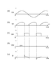
図4は、調光器が無い場合のインタフェース回路の主要な信号を例示する波形図であり、(a)は電源電圧VIN、(b)は検出電圧VR、(c)は第1の制御信号VB1、(d)は第2の制御信号VB2、(e)は電流IBである。
なお、本実施形態は、調光器がない構成のため、インタフェース回路1に入力される交流電圧VCTは、交流電源2の電源電圧VINと等しい。
Next, the operation of the interface circuit 1 will be described in the order of when there is no dimmer, when there is a dimmer 3a for phase control, and when there is a dimmer 3b for reverse phase control.
FIG. 4 is a waveform diagram illustrating main signals of the interface circuit when there is no dimmer, where (a) is the power supply voltage VIN, (b) is the detection voltage VR, and (c) is the first control signal. VB1, (d) is the second control signal VB2, and (e) is the current IB.
Since the present embodiment is configured without a dimmer, the AC voltage VCT input to the interface circuit 1 is equal to the power supply voltage VIN of the
交流電源2は、例えば周波数50Hz、電圧100Vの商用電源である。交流電源2の電源電圧VINがゼロクロスして、例えば、電源電圧VINが、入力端子5側を正極性、入力端子6側を負極性とする位相になっているとする。交流電圧VCT(=VIN)は、整流素子21を介して、スイッチング素子25のドレインに供給される。スイッチング素子25は、ノーマリオン形の素子のため、オンしている。
The
また、整流素子22は、遮断状態である。抵抗24の両端の電圧は、トランジスタ28のベース・エミッタ間に接続された抵抗32の両端の電圧よりも高い。その結果、整流回路10における入力端子10bと低電位端子10dとの間が導通状態になる。
検出電圧VRは、電源電圧VINの絶対値を、抵抗23、31で分割した電圧になり、電源電圧VINに応じて変化する(図4(a)、(b))。
Further, the rectifying
The detection voltage VR is a voltage obtained by dividing the absolute value of the power supply voltage VIN by the
また、第1の制御信号VB1は、ハイレベルであり(図4(c))、トランジスタ29はオンする。その結果、第1の回路43はオンに制御されて、第1の電流が一対の入力端子5、6の間に流れる(図4(e))。また、第2の制御信号VB2は、ローレベルであり(図4(d))、トランジスタ28はオフする。その結果、第2の回路44はオフに制御されて、第2の電流は遮断される。
The first control signal VB1 is at a high level (FIG. 4C), and the
時間が経過し電源電圧VINの位相が進むと、検出電圧VRは最大値を経て、しだいに減少していく(図4(a))。第1の回路43は、入力端子5、6の間に第1の電流を流す。
電源電圧VINがゼロクロスして、電源電圧VINの極性が反転して入力端子5側が負極性、入力端子6側が正極性になると、整流素子21がオフする。この場合の動作は、整流素子21、22の動作及び抵抗23、24の動作がそれぞれ入れ替わる点を除いて、上記と同様である。
As time elapses and the phase of the power supply voltage VIN advances, the detection voltage VR reaches its maximum value and gradually decreases (FIG. 4 (a)). The
When the power supply voltage VIN is zero-crossed and the polarity of the power supply voltage VIN is reversed so that the
次に、電源電圧VINがゼロクロスして、電源電圧VINの極性が反転して入力端子5側が正極性、入力端子6側が負極性になると、整流素子22がオフの状態に戻り、以下同様の動作を繰り返す。
Next, when the power supply voltage VIN is zero-crossed and the polarity of the power supply voltage VIN is reversed so that the
図5は、位相制御する調光器3aがある場合のインタフェース回路の主要な信号を例示する波形図であり、(a)は電源電圧VIN、(b)は検出電圧VR、(c)は第1の制御信号VB1、(d)は第2の制御信号VB2、(e)は電流IBである。
なお、本実施形態は、位相制御する調光器3aがある構成のため、インタフェース回路1に入力される交流電圧VCTは、調光器3aが導通状態のときに交流電源2の電源電圧VINと等しい。また、交流電源2は、周波数50Hz、電圧100Vの商用電源である。
FIG. 5 is a waveform diagram illustrating main signals of the interface circuit when there is a dimmer 3a for phase control, where (a) is a power supply voltage VIN, (b) is a detection voltage VR, and (c) is a first voltage. 1 control signal VB1, (d) is the second control signal VB2, and (e) is the current IB.
Since the present embodiment has a configuration with the dimmer 3a for phase control, the AC voltage VCT input to the interface circuit 1 is equal to the power supply voltage VIN of the
交流電源2の電源電圧VINがゼロクロスして、例えば、電源電圧VINが、入力端子5側を正極性、入力端子6側を負極性とする位相になっているとする(図5(a))。調光器3aは遮断状態のため、交流電圧VCTの絶対値は小さいままであり、電源電圧VINは、調光器3aに掛かっている。
Assume that the power supply voltage VIN of the
検出電圧VRが規定値V1より小さい期間は、第1の制御信号VB1として、ハイレベルが入力される(図5(b)、(c))。第1の回路43は、オンに制御され、入力端子5、6の間に第1の電流が流れる。また、検出電圧VRが規定値V1よりも小さい期間は、第2の制御信号VB2として、ローレベルが入力される(図5(b)、(d))。第2の回路44は、オフに制御され、第2の電流は流れない。その結果、入力端子5、6の間には、第1の電流が電流IBとして流れる(図5(e))。
During a period in which the detection voltage VR is smaller than the specified value V1, a high level is input as the first control signal VB1 (FIGS. 5B and 5C). The
交流電源2の電源電圧VINの絶対値が上昇して、調光器3aが導通すると、交流電圧VCTはほぼ電源電圧VINと等しくなる。その結果、検出電圧VRは規定値V1以上に上昇し(図5(b))、第1の制御信号VB1として、ローレベルが入力される(図5(c))。第1の回路43はオフに制御され、第1の電流は遮断される。
When the absolute value of the power supply voltage VIN of the
また、検出電圧VRが規定値V1以上になったとき、第2の制御信号VB2として、ハイレベルが入力される(図5(d))。第2の回路44にけるトランジスタ28はオンになり、抵抗26を介してコンデンサ30に充電電流が第2の電流として流れる。この充電電流によりコンデンサ30は充電されてスイッチング素子25のソース電位が上昇していく。スイッチング素子25のゲート・ソース間電圧(負極性)が、しきい値電圧よりも低下するとスイッチング素子25はオフする。その結果、第2の電流は、パルス電流として流れる(図5(e))。この第2の電流のピーク値は、第1の電流よりも大きく設定され、調光器3aを完全にオンさせる。
When the detection voltage VR becomes equal to or higher than the specified value V1, a high level is input as the second control signal VB2 (FIG. 5 (d)). The
電源電圧VINの位相が進み、検出電圧VRが規定値V1よりも小さくなる期間は、第1の制御信号VB1として、ハイレベルが入力される(図5(b)、(c))。第1の回路43はオンに制御され、第1の電流が入力端子5、6の間に流れる。また、この期間は、第2の制御信号VB2として、ローレベルが入力される(図5(b)、(d))。第2の回路44は、オフに制御される。なお、上記のとおり、第2の電流はパルス電流のため既に第1の電流に対して十分に小さくなっており、入力端子5、6の間の電流IBは、第1の電流になっている。
During a period in which the phase of the power supply voltage VIN advances and the detection voltage VR is smaller than the specified value V1, a high level is input as the first control signal VB1 (FIGS. 5B and 5C). The
電源電圧VINがゼロクロスして、電源電圧VINの極性が反転して入力端子5側が負極性、入力端子6側が正極性になると、整流素子21がオフする。この場合の動作は、整流素子21、22の動作及び抵抗23、24の動作がそれぞれ入れ替わる点を除いて、上記と同様である。
When the power supply voltage VIN is zero-crossed and the polarity of the power supply voltage VIN is reversed so that the
次に、電源電圧VINがゼロクロスして、電源電圧VINの極性が反転して入力端子5側が正極性、入力端子6側が負極性になると、整流素子22がオフの状態に戻り、以下同様の動作を繰り返す。
Next, when the power supply voltage VIN is zero-crossed and the polarity of the power supply voltage VIN is reversed so that the
なお、本実施形態においては、第2の回路44がコンデンサ30を有し、第2の制御信号VB2として、検出電圧VRが規定値V1以上のときにハイレベルとなる信号が入力される構成を例示している。しかし、第2の回路44からコンデンサ30を削除して、第2の制御信号VB2として、検出電圧VRが規定値V1以上になったときにハイレベルになる所定幅のパルス信号を入力してもよい。
In the present embodiment, the
図6は、逆位相制御する調光器3bがある場合のインタフェース回路の主要な信号を例示する波形図であり、(a)は電源電圧VIN、(b)は検出電圧VR、(c)は第1の制御信号VB1、(d)は第2の制御信号VB2、(e)は電流IBである。
なお、本実施形態は、逆位相制御する調光器3bがある構成のため、インタフェース回路1に入力される交流電圧VCTは、調光器3bが導通状態のときに交流電源2の電源電圧VINと等しい。また、交流電源2は、周波数50Hz、電圧100Vの商用電源である。
FIG. 6 is a waveform diagram illustrating main signals of the interface circuit when there is a dimmer 3b that performs antiphase control. FIG. 6A is a power supply voltage VIN, FIG. 6B is a detection voltage VR, and FIG. The first control signal VB1, (d) is the second control signal VB2, and (e) is the current IB.
In the present embodiment, since the dimmer 3b that performs antiphase control is provided, the AC voltage VCT input to the interface circuit 1 is the power supply voltage VIN of the
交流電源2の電源電圧VINがゼロクロスして、例えば、電源電圧VINが、入力端子5側を正極性、入力端子6側を負極性とする位相になっているとする(図6(a))。調光器3bは遮断状態のため、交流電圧VCTの絶対値は小さいままであり、電源電圧VINは、調光器3bに掛かっている。
Assume that the power supply voltage VIN of the
交流電源2の電源電圧VINがゼロクロスして、例えば、電源電圧VINが、入力端子5側を正極性、入力端子6側を負極性とする位相になっている状態から、電源電圧VINが上昇して、検出電圧VRが規定値V1に達するまでの動作は、導通状態の調光器3bを介して電源電圧VINとほぼ等しい交流電圧VCTが入力端子5、6に入力されている点以外は、図4を参照して説明した調光器がない場合と同様である。
The power supply voltage VIN rises from the state where the power supply voltage VIN of the
検出電圧VRが規定値V1よりも小さい期間は、第1の制御信号VB1として、ハイレベルが入力される(図6(b)、(c))。第1の回路43は、オンに制御され、入力端子5、6の間に第1の電流が流れる。また、検出電圧VRに依存せずに、第2の制御信号VB2として、ローベルが入力される(図6(d))。その結果、第2の回路44はオフに制御され、第2の電流は遮断されている。
During a period in which the detection voltage VR is smaller than the specified value V1, a high level is input as the first control signal VB1 (FIGS. 6B and 6C). The
時間が経過し電源電圧VINの位相が進むと、検出電圧VRが規定値V1以上に上昇する(図6(b))。第1の制御信号VB1として、ローレベルが入力される(図6(c))。第1の回路43は、オフに制御され、入力端子5、6間の第1の電流は遮断される。なお、上記のとおり、第2の制御信号VB2として、常にローレベルが入力されるため(図6(d))、第2の回路44は、オフに制御され、第2の電流は遮断されている。その結果、入力端子5、6間の電流IBはゼロになる(図6(e))。
When time elapses and the phase of the power supply voltage VIN advances, the detection voltage VR rises to a specified value V1 or more (FIG. 6B). A low level is input as the first control signal VB1 (FIG. 6C). The
また、時間が経過し電源電圧VINの位相が進むと、調光器3bが遮断状態になり、検出電圧VRは低下していく(図6(b))。このとき、少なくとも検出電圧VRが規定値V1以下になるまでの期間は、第1の制御信号VB1として、ハイレベルが入力される(図6(c))。第1の回路43は、入力端子5、6の間に第1の電流を流す。その結果、入力端子5、6間に接続された雑音防止用のコンデンサなどに蓄積された電荷が放電されて、入力端子5、6に入力される交流電圧VCTを速やかにゼロに低下させることができる。
Further, when time elapses and the phase of the power supply voltage VIN advances, the dimmer 3b is cut off and the detection voltage VR decreases (FIG. 6B). At this time, a high level is input as the first control signal VB1 at least until the detection voltage VR becomes equal to or lower than the specified value V1 (FIG. 6C). The
時間が経過し電源電圧VINがゼロクロスして、電源電圧VINの極性が反転して入力端子5側が負極性、入力端子6側が正極性になると、整流素子21がオフする。この場合の動作は、整流素子21、22の動作及び抵抗23、24の動作がそれぞれ入れ替わる点を除いて、上記と同様である。
When time elapses and the power supply voltage VIN is zero-crossed and the polarity of the power supply voltage VIN is reversed and the
次に、電源電圧VINがゼロクロスして、電源電圧VINの極性が反転して入力端子5側が正極性、入力端子6側が負極性になると、整流素子22がオフの状態に戻り、以下同様の動作を繰り返す。
Next, when the power supply voltage VIN is zero-crossed and the polarity of the power supply voltage VIN is reversed so that the
なお、本実施形態においては、検出電圧VRが規定値V1以上の期間は、第1の制御信号VB1として、ローレベルが入力され、第1の回路43がオフに制御され構成を例示した。しかし、調光器3bが遮断状態になったときに、検出電圧VRが規定値V1以上の期間における、少なくとも検出電圧VRが規定値V1以下になるまでの期間に第1の回路43がオンに制御できればよく、例えば、検出電圧VRが規定値V1以上の期間にも、第1の制御信号VB1として、ハイレベルが入力されて、第1の回路43をオンに制御する構成としてもよい。
In the present embodiment, the configuration in which the low level is input as the first control signal VB1 and the
本実施形態においては、調光器の有無及び種類に応じて入力される第1の制御信号VB1、第2の制御信号VB2により入力端子5、6間に流れる電流IBが制御されるため、調光器を安定動作させることができる。
In the present embodiment, the current IB flowing between the
また、本実施形態においては、調光器が位相制御する調光器3aの場合に対応して、調光器3aが遮断状態のときに第1の電流を流すため、交流電圧VCTをゼロ近傍に低下させることができる。その結果、調光器3aを確実に遮断状態にすることができる。また、調光器3aが導通状態になった直後に第1の電流よりも大きい第2の電流を流すため、調光器3aの導通状態がばらつくことなく、調光器3aを確実に導通状態にすることができる。 Further, in the present embodiment, in correspondence with the case of the dimmer 3a whose phase is controlled by the dimmer, since the first current flows when the dimmer 3a is in the cut-off state, the AC voltage VCT is set to near zero. Can be lowered. As a result, the dimmer 3a can be reliably turned off. In addition, since the second current larger than the first current flows immediately after the dimmer 3a is turned on, the dimmer 3a is surely turned on without causing the conductive state of the dimmer 3a to vary. Can be.
また、本実施形態においては、調光器が逆位相制御する調光器3bの場合に対応して、調光器3bが導通状態から遮断状態になるときに、第1の電流を流すため、入力端子5、6間に接続されたノイズ除去用のコンデンサなどに蓄積された電荷を放電させることができる。その結果、交流電圧VCTをゼロ近傍に低下させて、調光器3bを確実に遮断状態にすることができる。
Further, in the present embodiment, since the dimmer 3b is switched from the conductive state to the cut-off state in response to the dimmer 3b whose anti-phase control is performed by the dimmer, the first current is caused to flow. Charges accumulated in a noise removing capacitor connected between the
なお、本実施形態においては、インタフェース回路1の外部にマイクロプロセッサ(MPU)32が設けられ、交流電圧の絶対値を検出して検出電圧VRとして外部に接続されたマイクロプロセッサ32に出力し、またマイクロプロセッサ32から入力される第1の制御信号VB1、第2の制御信号VB2などにより制御される構成を例示している。しかし、第1の制御信号VB1、第2の制御信号VB2をインタフェース回路1の内部で生成する構成も可能である。
In this embodiment, a microprocessor (MPU) 32 is provided outside the interface circuit 1 to detect the absolute value of the AC voltage and output it to the
(第2の実施形態)
図7は、第2の実施形態に係るインタフェース回路を例示する回路図である。
本実施形態のインタフェース回路1aにおいては、第1の実施形態のインタフェース回路1に、制御回路20が追加されている。インタフェース回路1aにおける制御回路20以外の構成は、インタフェース回路1の構成と同様である。
(Second Embodiment)
FIG. 7 is a circuit diagram illustrating an interface circuit according to the second embodiment.
In the
制御回路20は、例えばマイクロプロセッサであり、外部から調光器の有無及び種類を示す信号を入力して、第1の制御信号VB1、第2の制御信号VB2を生成する。ここで、調光器の有無及び種類を示す信号は、例えば、交流電圧VCTが調光器3bにより逆位相制御されていることを示す第1の信号、交流電圧VCTが調光器3aにより位相制御されていることを示す第2の信号、調光器がなく交流電圧VCTの位相連続していることを示す第3の信号である。例えば、第1の信号は端子33f、第2の信号は端子33g、第3の信号は端子33hをそれぞれ介して入力される。なお、制御回路20は、第1の実施形態におけるインタフェース回路の外部に接続されたマイクロプロセッサと同一の構成とすることができる。
The
図8は、インタフェース回路における負荷回路の動作を例示する模式図である。
第1の回路43、第2の回路44は、制御回路20から出力される第1の制御信号VB1、第2の制御信号VB2をそれぞれ入力して、図8に表したように動作する。
FIG. 8 is a schematic view illustrating the operation of the load circuit in the interface circuit.
The
調光器の有無及び種類については、交流電源が、例えば商用電源の場合など、一度検出しておけば比較的長期間、同一である場合が多く、外部から、例えば、第1〜第3の信号として設定することができる。調光器の有無及び種類に対応して、制御回路20が第1の制御信号VB1、第2の制御信号VB2を生成するため、取り扱いが容易になる。
このように、本実施形態においては、制御回路20が設けられているため、調光器の有無及び種類に対応することが容易になる。
As for the presence and type of the dimmer, the AC power source is often the same for a relatively long period of time once detected, for example, in the case of a commercial power source. It can be set as a signal. Since the
Thus, in this embodiment, since the
(第3の実施形態)
図9は、第3の実施形態に係るインタフェース回路を例示する回路図である。
本実施形態のインタフェース回路1bにおいては、第2の実施形態のインタフェース回路1aにおける制御回路20の替わりに、制御回路20aが設けられ、さらに電源回路45が追加されている。インタフェース回路1bにおける制御回路20a及び電源回路45以外の構成は、インタフェース回路1aの構成と同様である。
(Third embodiment)
FIG. 9 is a circuit diagram illustrating an interface circuit according to the third embodiment.
In the
制御回路20aは、制御回路20と比較して、調光器の有無及び種類を示す第1〜第3の信号が入力されず、検出電圧VR、高電位端子10cの電位を入力して、第1の制御信号VB1、第2の制御信号VB2を生成する点が異なる。制御回路20aは、例えばマイクロプロセッサで構成される。
Compared with the
電源回路45は、制御回路20aに電源を供給する。電源回路45は、抵抗46、50、コンデンサ47、ツェナーダイオード48、ダイオード49、トランジスタ51を有している。抵抗46とコンデンサ47は、平滑回路を構成し、制御回路20aに平滑化した電圧を供給する。また、ツェナーダイオード48とトランジスタ51は、安定化電源を構成している。ダイオード49は、保護ダイオードである。なお、本実施形態では、トランジスタ51としてPNPトランジスタを用い、ツェナーダイオード48で基準電圧を生成する構成を例示したが、制御回路に安定化した電圧を供給できれば他の構成でもよい。
The
図10は、制御回路の動作を説明するフローチャートである。
まず、制御回路20aは、検出電圧VRを入力して、傾きdVR/dtを求める(ステップS1)。
次に、求めた傾きdVR/dtの絶対値|dVR/dt|と、所定値とを比較して、傾きの絶対値|dVR/dt|が、所定値以上であるかを求める(ステップS2)。
FIG. 10 is a flowchart for explaining the operation of the control circuit.
First, the
Next, the absolute value | dVR / dt | of the obtained slope dVR / dt is compared with a predetermined value to determine whether the absolute value | dVR / dt | of the slope is equal to or larger than the predetermined value (step S2). .
傾きの絶対値|dVR/dt|が、所定値以上の場合は、調光器があると判断する(ステップS2:Yes)。交流電圧VCTが調光器3aにより位相制御されている場合、調光器3aが遮断状態から導通状態に変化するときに検出電圧VRの傾きが急変する。また、調光器3bにより逆位相制御されている場合、調光器3bが導通状態から遮断状態に変化するときに検出電圧VRの傾きが急変する。一方、調光器がない場合は、検出電圧VRはほぼ正弦波であり、検出電圧VRの傾きは急変せず、所定値よりも小さくなる。そこで、本実施形態においては、傾きの絶対値|dVR/dt|が、所定値以上の場合は、調光器があると判断し(ステップS2:Yes)、所定値よりも小さい場合は、調光器がないと判断する(ステップS2:No)。 If the absolute value | dVR / dt | of the slope is equal to or greater than a predetermined value, it is determined that there is a dimmer (step S2: Yes). When the AC voltage VCT is phase-controlled by the dimmer 3a, the slope of the detection voltage VR changes suddenly when the dimmer 3a changes from the cut-off state to the conductive state. In addition, when the anti-phase control is performed by the dimmer 3b, the slope of the detection voltage VR changes suddenly when the dimmer 3b changes from the conductive state to the cutoff state. On the other hand, when there is no dimmer, the detection voltage VR is almost a sine wave, and the slope of the detection voltage VR does not change suddenly and becomes smaller than a predetermined value. Therefore, in the present embodiment, if the absolute value | dVR / dt | of the slope is equal to or greater than a predetermined value, it is determined that there is a dimmer (step S2: Yes), and if the absolute value | dVR / dt | It is determined that there is no optical device (step S2: No).
調光器がないと判断された場合は(ステップS2:No)、ステップS3に進み、第1の回路43をオンに制御する第1の制御信号VB1、第2の回路44をオフに制御する第2の制御信号VB2を生成して終了する(ステップS3)。
When it is determined that there is no dimmer (step S2: No), the process proceeds to step S3, and the first control signal VB1 for controlling the
また、調光器があると判断された場合は(ステップS2:Yes)、ステップS4に進み、検出電圧VRの規定値V1における傾きdVR/dtが所定値以上かを求める(ステップS4)。 If it is determined that there is a dimmer (step S2: Yes), the process proceeds to step S4, and it is determined whether the slope dVR / dt at the specified value V1 of the detection voltage VR is equal to or greater than a predetermined value (step S4).
検出電圧VRの規定値V1における傾きdVR/dtが所定値以上の場合は、交流電圧VCTは、調光器3aにより位相制御されていると判断する(ステップS4:Yes)。交流電圧VCTが調光器3aにより位相制御されている場合、調光器3aが遮断状態から導通状態に変化して、検出電圧VRが規定値V1以上になるときに検出電圧VRの傾きが急変する。また、調光器3bにより逆位相制御されている場合、検出電圧VRが規定値V1以上になるときは調光器がない場合と同様に検出電圧VRの傾きは急変しない。そこで、検出電圧VRの規定値V1における傾きdVR/dtが所定値以上の場合は、交流電圧VCTが調光器3aにより位相制御されていると判断し(ステップS4:Yes)、所定値よりも小さい場合は、交流電圧VCTが調光器3bにより逆位相制御されていると判断する(ステップS4:No)。 When the slope dVR / dt at the specified value V1 of the detection voltage VR is equal to or greater than a predetermined value, it is determined that the AC voltage VCT is phase-controlled by the dimmer 3a (step S4: Yes). When the AC voltage VCT is phase-controlled by the dimmer 3a, the slope of the detection voltage VR changes suddenly when the dimmer 3a changes from the cut-off state to the conduction state and the detection voltage VR becomes equal to or higher than the specified value V1. To do. In addition, when the anti-phase control is performed by the dimmer 3b, the slope of the detection voltage VR does not change abruptly when the detection voltage VR becomes equal to or higher than the specified value V1 as in the case where there is no dimmer. Therefore, if the slope dVR / dt of the detection voltage VR at the specified value V1 is equal to or greater than a predetermined value, it is determined that the AC voltage VCT is phase-controlled by the dimmer 3a (step S4: Yes), and is greater than the predetermined value. If it is smaller, it is determined that the AC voltage VCT is controlled in reverse phase by the dimmer 3b (step S4: No).
交流電圧VCTが調光器3aにより位相制御されていると判断された場合は(ステップS4:Yes)、ステップS5に進み、第1の回路43を、検出電圧VRが規定値V1よりも小さいときはオンに制御し、検出電圧VRが規定値V1以上のときはオフに制御する第1の制御信号VB1を生成する(ステップS5)。また、第2の回路44を、検出電圧VRが規定値V1以上になったときに、所定期間オンに制御する第2の制御信号VB2を生成して終了する(ステップS5)。
When it is determined that the AC voltage VCT is phase-controlled by the dimmer 3a (step S4: Yes), the process proceeds to step S5, and the
交流電圧VCTが調光器3bにより逆位相制御されていると判断された場合は(ステップS4:No)、ステップS6に進み、第1の回路43を、検出電圧VRが規定値V1よりも小さいときはオンに制御し、検出電圧VRが規定値V1以上のときは、少なくとも検出電圧VRが低下して検出電圧VRが規定値V1以下になるまでオンに制御する第1の制御信号VB1を生成する(ステップS6)。また、第2の回路44を、オフに制御する第2の制御信号VB2を生成して終了する(ステップS6)。
If it is determined that the AC voltage VCT is controlled in reverse phase by the dimmer 3b (step S4: No), the process proceeds to step S6, and the detection voltage VR is smaller than the specified value V1 in the
本実施形態においては、検出電圧VRの傾きdVR/dtに基づいて、調光器の有無を検出し、検出電圧VRが規定値V1以上に上昇するときの検出電圧VRの傾きに基づいて、交流電圧VCTが位相制御、逆位相制御されているかを検出する。 In the present embodiment, the presence or absence of a dimmer is detected based on the slope dVR / dt of the detection voltage VR, and the alternating current is based on the slope of the detection voltage VR when the detection voltage VR rises to a specified value V1 or more. It is detected whether the voltage VCT is subjected to phase control or antiphase control.
図11は、制御回路の動作を説明する他のフローチャートである。
まず、制御回路20aは、検出電圧VRを入力して、検出電圧VRが規定値V1以下の期間の幅を求める(ステップS11)。
次に、求めた期間の長さと、所定値とを比較して、期間の長さが、所定値以上であるかを求める(ステップS12)。
FIG. 11 is another flowchart for explaining the operation of the control circuit.
First, the
Next, the determined length of the period is compared with a predetermined value to determine whether the length of the period is equal to or greater than the predetermined value (step S12).
期間の長さが、所定値以上の場合は、調光器があると判断する(ステップS12:Yes)。
図2を参照して説明したように、位相制御する調光器3aは、検出電圧VRが規定値V1以下である期間の最小時間幅は、交流電圧VCTの周期(電源電圧VINの半周期)の10%〜25%である。交流電源2の周波数が50Hzの場合においては、半周期は10msであり、最小時間幅は、例えば1ms〜2.5msになる。また、図3を参照して説明したように、逆位相制御する調光器3bは、検出電圧VRが規定値V1以下である期間の最小幅は、交流電圧VCTの周期(電源電圧VINの半周期)の10%〜35%である。交流電源2の周波数が50Hzの場合においては、最小時間幅は、例えば1ms〜2.5msになる。
If the length of the period is equal to or greater than the predetermined value, it is determined that there is a dimmer (step S12: Yes).
As described with reference to FIG. 2, in the dimmer 3 a that controls the phase, the minimum time width of the period in which the detection voltage VR is equal to or less than the specified value V1 is the period of the AC voltage VCT (half period of the power supply voltage VIN). 10% to 25%. When the frequency of the
したがって、検出電圧VRが規定値V1以下である期間を、例えば調光器がない場合の値に対してしきい値0.5msで判定することにより、調光器の有無を検出することができる。そこで、本具体例においては、検出電圧VRが規定値V1以下である期間の長さが、所定値以上の場合は、調光器があると判断し(ステップS12:Yes)、所定値よりも小さい場合は、調光器がないと判断する(ステップS12:No)。 Therefore, the presence or absence of the dimmer can be detected by determining the period during which the detection voltage VR is equal to or less than the specified value V1, for example, with a threshold value of 0.5 ms with respect to the value when there is no dimmer. . Therefore, in this specific example, if the length of the period during which the detection voltage VR is equal to or less than the specified value V1 is equal to or greater than a predetermined value, it is determined that there is a dimmer (step S12: Yes), and is greater than the predetermined value. If it is smaller, it is determined that there is no dimmer (step S12: No).
調光器がないと判断された場合は(ステップS12:No)、ステップS3に進み、第1の回路43をオンに制御する第1の制御信号VB1、第2の回路44をオフに制御する第2の制御信号VB2を生成して終了する(ステップS3)。なお、ステップS3は、図10を参照して説明したステップS3と同様である。
When it is determined that there is no dimmer (step S12: No), the process proceeds to step S3, and the first control signal VB1 for controlling the
また、調光器があると判断された場合は(ステップS12:Yes)、ステップS13に進み、検出電圧VRが規定値V1以上になった直後の検出電圧VRを求める(ステップS13)。
次に、検出電圧VRが規定値V1以上になった直後の検出電圧VRが所定値以上かを求める(ステップS14)。
If it is determined that there is a dimmer (step S12: Yes), the process proceeds to step S13, and the detection voltage VR immediately after the detection voltage VR becomes equal to or higher than the specified value V1 is obtained (step S13).
Next, it is determined whether or not the detected voltage VR immediately after the detected voltage VR becomes equal to or higher than the specified value V1 (step S14).
図10のステップS4を参照して説明したように、交流電圧VCTが調光器3aにより位相制御されている場合、調光器3aが遮断状態から導通状態に変化して、検出電圧VRが規定値V1以上になるときに検出電圧VRの傾きが急変する。その結果、検出電圧VRが規定値V1以上になった直後の検出電圧VRは、相対的に大きい値になる。また、調光器3bにより逆位相制御されている場合、検出電圧VRが規定値V1以上になるときは調光器がない場合と同様に検出電圧VRの傾きは急変しない。その結果、検出電圧VRが規定値V1以上になった直後の検出電圧VRは、相対的に小さい値になる。そこで、検出電圧VRが規定値V1以上になった直後の検出電圧VRが所定値以上の場合は、交流電圧VCTが調光器3aにより位相制御されていると判断し(ステップS14:Yes)、所定値よりも小さい場合は、交流電圧VCTが調光器3bにより逆位相制御されていると判断する(ステップS14:No)。 As described with reference to step S4 of FIG. 10, when the AC voltage VCT is phase-controlled by the dimmer 3a, the dimmer 3a changes from the cut-off state to the conductive state, and the detection voltage VR is defined. The slope of the detection voltage VR changes suddenly when the value V1 or more. As a result, the detection voltage VR immediately after the detection voltage VR becomes equal to or higher than the specified value V1 becomes a relatively large value. In addition, when the anti-phase control is performed by the dimmer 3b, the slope of the detection voltage VR does not change abruptly when the detection voltage VR becomes equal to or higher than the specified value V1 as in the case where there is no dimmer. As a result, the detection voltage VR immediately after the detection voltage VR becomes equal to or higher than the specified value V1 is a relatively small value. Therefore, if the detection voltage VR immediately after the detection voltage VR becomes equal to or higher than the specified value V1 is equal to or higher than the predetermined value, it is determined that the AC voltage VCT is phase-controlled by the dimmer 3a (step S14: Yes). If it is smaller than the predetermined value, it is determined that the AC voltage VCT is controlled in reverse phase by the dimmer 3b (step S14: No).
交流電圧VCTが調光器3aにより位相制御されていると判断された場合は(ステップS14:Yes)、ステップS5に進み、第1の回路43を、検出電圧VRが規定値V1よりも小さいときはオンに制御し、検出電圧VRが規定値V1以上のときはオフに制御する第1の制御信号VB1を生成する(ステップS5)。また、第2の回路44を、検出電圧VRが規定値V1以上になったときに、所定期間オンに制御する第2の制御信号VB2を生成して終了する(ステップS5)。なお、ステップS5は、図10を参照して説明したステップS5と同様である。
When it is determined that the phase of the AC voltage VCT is controlled by the dimmer 3a (step S14: Yes), the process proceeds to step S5, and the
交流電圧VCTが調光器3bにより逆位相制御されていると判断された場合は(ステップS14:No)、ステップS6に進み、第1の回路43を、検出電圧VRが規定値V1よりも小さいときはオンに制御し、検出電圧VRが規定値V1以上のときは、少なくとも検出電圧VRが低下して検出電圧VRが規定値V1以下になるまでオンに制御する第1の制御信号VB1を生成する(ステップS6)。また、第2の回路44を、オフに制御する第2の制御信号VB2を生成して終了する(ステップS6)。なお、ステップS6は、図10を参照して説明したステップS6と同様である。
When it is determined that the AC voltage VCT is controlled in reverse phase by the dimmer 3b (step S14: No), the process proceeds to step S6, and the detection voltage VR is smaller than the specified value V1 in the
本実施形態においては、検出電圧VRが規定値V1以下の期間の長さに基づいて、調光器の有無を検出し、検出電圧VRが規定値V1以上になった直後の検出電圧VRに基づいて、交流電圧VCTが位相制御されているか、または逆位相制御されているかを検出する。 In the present embodiment, the presence or absence of a dimmer is detected based on the length of the period in which the detection voltage VR is equal to or less than the specified value V1, and based on the detection voltage VR immediately after the detection voltage VR becomes equal to or greater than the specified value V1. Thus, it is detected whether the AC voltage VCT is phase-controlled or anti-phase-controlled.
なお、上記においては、検出電圧VRが規定値V1以下の期間の長さ、または、検出電圧VRの傾きdVR/dtに基づいて、調光器の有無を検出する具体例について説明した。また、検出電圧VRが規定値V1以上になった直後の検出電圧VR、または検出電圧VRが規定値V1以上になるときの検出電圧VRの傾きに基づいて、調光器の種類祖検出する具体例について説明した。しかし、上記の実施形態で説明した組み合わせの他に、他の任意の組合で用いることができる。 In the above description, the specific example in which the presence or absence of the dimmer is detected based on the length of the period in which the detection voltage VR is equal to or less than the specified value V1 or the gradient dVR / dt of the detection voltage VR has been described. Further, based on the detection voltage VR immediately after the detection voltage VR becomes equal to or higher than the specified value V1 or the inclination of the detection voltage VR when the detection voltage VR becomes equal to or higher than the specified value V1, the type of the dimmer is detected. An example was described. However, in addition to the combinations described in the above embodiments, other arbitrary combinations can be used.
本実施形態においては、検出電圧が規定値V1より小さいときの期間の長さと、検出電圧VRの傾きdVR/dt及び検出電圧VRが規定値V1以上に上昇した直後の電圧値の少なくともいずれかに基づいて、交流電圧VCTが位相制御、逆位相制御または位相連続しているかを検出し、第1の制御信号VB1、第2の制御信号VB2を生成する。その結果、外部から調光器の有無及び種類を示す信号を入力することなく、第1の実施形態と同様の効果を得ることができる。 In the present embodiment, at least one of the length of the period when the detected voltage is smaller than the specified value V1, the slope dVR / dt of the detected voltage VR, and the voltage value immediately after the detected voltage VR rises to the specified value V1 or more. Based on this, it is detected whether the AC voltage VCT is phase-controlled, anti-phase-controlled, or phase-continuous, and the first control signal VB1 and the second control signal VB2 are generated. As a result, the same effect as that of the first embodiment can be obtained without inputting a signal indicating the presence and type of the dimmer from the outside.
以上、具体例を参照しつつ実施形態について説明したが、それらに限定されるものではなく、種々の変形が可能である。 As described above, the embodiments have been described with reference to specific examples. However, the embodiments are not limited thereto, and various modifications are possible.
例えば、各実施形態において、第1の制御信号VB1、第2の制御信号VB2が、ハイレベルとローレベルとの二値信号を用いる構成を例示した。しかし、第1の制御信号VB1、第2の制御信号VB2は、例えば連続的に変化可能なアナログ信号、例えば段階的に変化可能な多値信号を用いて、第1の電流の電流値、第2の電流の電流値を制御する構成とすることもできる。例えば、検出電圧VRが増加すると第1の電流が減少するように第1の制御信号VB1を変化させて、第1の回路43に定電力特性を持たせる構成とすることもできる。例えば、調光器がない場合など、第1の回路43が連続的にオンに制御されるため、定電力特性とすることにより消費電力を低減することができる。
For example, in each embodiment, the configuration in which the first control signal VB1 and the second control signal VB2 use binary signals of a high level and a low level is exemplified. However, the first control signal VB1 and the second control signal VB2 are, for example, analog signals that can be changed continuously, for example, multilevel signals that can be changed stepwise, The current value of the second current can also be controlled. For example, the
また、スイッチング素子25は、ノーマリオン形の素子であればよく、MOSFETの他にHEMTを用いることができる。また、HEMTは、GaN系HEMTには限定されない。例えば、半導体基板に炭化珪素(SiC)や窒化ガリウム(GaN)やダイヤモンドのようなワイドバンドギャップを有する半導体(ワイドバンドギャップ半導体)を用いて形成した半導体素子でもよい。ここで、ワイドバンドギャップ半導体とは、バンドギャップが約1.4eVのヒ化ガリウム(GaAs)よりもバンドギャップの広い半導体をいう。例えば、バンドギャップが1.5eV以上の半導体、リン化ガリウム(GaP、バンドギャップ約2.3eV)、窒化ガリウム(GaN、バンドギャップ約3.4eV)、ダイアモンド(C、バンドギャップ約5.27eV)、窒化アルミニウム(AlN、バンドギャップ約5.9eV)、炭化ケイ素(SiC)などが含まれる。このようなワイドバンドギャップ半導体素子は、耐圧を等しくする場合、シリコン半導体素子よりも小さくできるため、インタフェース回路の小形化が可能となる。
The switching
本発明のいくつかの実施形態および実施例を説明したが、これらの実施形態または実施例は、例として提示したものであり、発明の範囲を限定することは意図していない。これら新規な実施形態または実施例は、その他の様々な形態で実施されることが可能であり、発明の要旨を逸脱しない範囲で、種々の省略、置き換え、変更を行うことができる。これら実施形態または実施例やその変形は、発明の範囲や要旨に含まれるとともに、特許請求の範囲に記載された発明とその均等の範囲に含まれる。 Although several embodiments and examples of the present invention have been described, these embodiments or examples are presented as examples and are not intended to limit the scope of the invention. These novel embodiments or examples can be implemented in various other forms, and various omissions, replacements, and changes can be made without departing from the spirit of the invention. These embodiments or examples and modifications thereof are included in the scope and gist of the invention, and are included in the invention described in the claims and the equivalents thereof.
1、1a、1b…インタフェース回路、 2…交流電源、 3、3a、3b…調光器、 4…照明機器、 5、6…入力端子、 8、9…出力端子、 10、40…整流回路、 10a、10b…入力端子(整流回路の入力端子)、 10c…高電位端子、 10d…低電位端子、 11…平滑コンデンサ、 12…トライアック、 13…位相回路、 14…ダイアック、 15…可変抵抗、 16…タイミングコンデンサ、 17…チョークコイル、 18、30、39、47…コンデンサ、 19…負荷回路、 20、20a…制御回路、 21、22…整流素子、 23…第1の抵抗、 24…第2の抵抗、 25…スイッチング素子、 26、27、32、38、46…抵抗、 31…第3の抵抗、 28、29…トランジスタ、 33a、33b、33c、33d、33e、33f…制御端子、33g、33h…端子、 34、40…整流回路、 35…半導体スイッチ、 36…フォトカプラ、 36a…受光素子、 36b…発光素子、 37、49…ダイオード、 41…調光制御回路、 42…検出回路、 43…第1の回路、 44…第2の回路、 45…電源回路、 48…ツェナーダイオード、 49…ダイオード、 51…トランジスタ、 100…インダクタ、 101…フィルタコンデンサ
DESCRIPTION OF
Claims (9)
前記交流電圧を検出して検出電圧として出力する検出回路と、
入力される第1の制御信号に基づいてオンまたはオフに制御され、オンのとき前記一対の入力端子間に第1の電流を流し、オフのとき前記第1の電流を遮断する第1の回路と、
入力される第2の制御信号に基づいてオンまたはオフに制御され、オンのとき前記一対の入力端子間に前記第1の電流よりも大きい第2の電流を流し、オフのとき前記第2の電流を遮断する第2の回路と、
前記第1の制御信号と前記第2の制御信号とを生成する制御回路と、
を備え、
前記調光器によって逆位相制御された前記交流電圧が入力される場合には、
前記第1の回路は、前記検出電圧が規定値よりも小さいときはオンに制御され、前記検出電圧が前記規定値以上のときは、少なくとも前記検出電圧が低下して前記検出電圧が前記規定値以下になるまでオンに制御され、
前記第2の回路は、オフに制御されるインタフェース回路。 A rectifier circuit that rectifies an alternating voltage input between a pair of input terminals and is phase-controlled or reversed-phase controlled by a dimmer, or a phase-continuous alternating voltage that does not pass through a dimmer;
A detection circuit that detects the alternating voltage and outputs it as a detection voltage;
A first circuit that is controlled to be turned on or off based on a first control signal that is input, and that causes a first current to flow between the pair of input terminals when turned on and blocks the first current when turned off. When,
The second control signal is controlled to be turned on or off based on the input second control signal, and when turned on, a second current larger than the first current flows between the pair of input terminals, and when turned off, the second current is passed. A second circuit for interrupting the current;
A control circuit for generating the first control signal and the second control signal;
With
When the AC voltage that is antiphase controlled by the dimmer is input,
The first circuit is controlled to be on when the detected voltage is smaller than a specified value, and when the detected voltage is equal to or higher than the specified value, at least the detected voltage is lowered and the detected voltage is set to the specified value. Controlled on until
The second circuit is an interface circuit controlled to be turned off .
前記第1の回路は、前記検出電圧が規定値よりも小さいときはオンに制御され、前記検出電圧が前記規定値以上のときはオフに制御され、
前記第2の回路は、前記検出電圧が前記規定値以上になったときに、所定期間オンに制御される請求項1記載のインタフェース回路。 When the AC voltage phase-controlled by the dimmer is input,
The first circuit is controlled to be on when the detection voltage is smaller than a specified value, and is controlled to be off when the detection voltage is equal to or higher than the specified value.
The interface circuit according to claim 1, wherein the second circuit is controlled to be turned on for a predetermined period when the detection voltage becomes equal to or higher than the specified value.
前記第1の回路は、オンに制御され、
前記第2の回路は、オフに制御される請求項1記載のインタフェース回路。 When the AC voltage is input without going through the dimmer,
The first circuit is controlled to be on;
The interface circuit according to claim 1, wherein the second circuit is controlled to be turned off.
前記交流電圧を検出して検出電圧として出力する検出回路と、
入力される第1の制御信号に基づいてオンまたはオフに制御され、オンのとき前記一対の入力端子間に第1の電流を流し、オフのとき前記第1の電流を遮断する第1の回路と、
入力される第2の制御信号に基づいてオンまたはオフに制御され、オンのとき前記一対の入力端子間に前記第1の電流よりも大きい第2の電流を流し、オフのとき前記第2の電流を遮断する第2の回路と、
を備え、
前記第1の回路は、前記検出電圧が増加すると前記第1の電流が減少する定電力特性を有するインタフェース回路。 A rectifier circuit that rectifies an alternating voltage input between a pair of input terminals and is phase-controlled or reversed-phase controlled by a dimmer, or a phase-continuous alternating voltage that does not pass through a dimmer;
A detection circuit that detects the alternating voltage and outputs it as a detection voltage;
A first circuit that is controlled to be turned on or off based on a first control signal that is input, and that causes a first current to flow between the pair of input terminals when turned on and blocks the first current when turned off. When,
The second control signal is controlled to be turned on or off based on the input second control signal, and when turned on, a second current larger than the first current flows between the pair of input terminals, and when turned off, the second current is passed. A second circuit for interrupting the current;
With
The first circuit is an interface circuit having a constant power characteristic in which the first current decreases as the detection voltage increases.
前記調光器によって逆位相制御された前記交流電圧が入力される場合には、 When the AC voltage that is antiphase controlled by the dimmer is input,
前記第1の回路は、前記検出電圧が規定値よりも小さいときはオンに制御され、前記検出電圧が前記規定値以上のときは、少なくとも前記検出電圧が低下して前記検出電圧が前記規定値以下になるまでオンに制御され、 The first circuit is controlled to be on when the detected voltage is smaller than a specified value, and when the detected voltage is equal to or higher than the specified value, at least the detected voltage is lowered and the detected voltage is set to the specified value. Controlled on until
前記第2の回路は、オフに制御される請求項5記載のインタフェース回路。 The interface circuit according to claim 5, wherein the second circuit is controlled to be turned off.
前記調光器によって位相制御された前記交流電圧が入力される場合には、 When the AC voltage phase-controlled by the dimmer is input,
前記第1の回路は、前記検出電圧が規定値よりも小さいときはオンに制御され、前記検出電圧が前記規定値以上のときはオフに制御され、 The first circuit is controlled to be on when the detection voltage is smaller than a specified value, and is controlled to be off when the detection voltage is equal to or higher than the specified value.
前記第2の回路は、前記検出電圧が前記規定値以上になったときに、所定期間オンに制御される請求項5記載のインタフェース回路。 The interface circuit according to claim 5, wherein the second circuit is controlled to be turned on for a predetermined period when the detected voltage becomes equal to or higher than the specified value.
前記調光器を介さずに前記交流電圧が入力される場合には、 When the AC voltage is input without going through the dimmer,
前記第1の回路は、オンに制御され、 The first circuit is controlled to be on;
前記第2の回路は、オフに制御される請求項5記載のインタフェース回路。 The interface circuit according to claim 5, wherein the second circuit is controlled to be turned off.
Priority Applications (4)
| Application Number | Priority Date | Filing Date | Title |
|---|---|---|---|
| JP2012167632A JP6035954B2 (en) | 2012-07-27 | 2012-07-27 | Interface circuit |
| US13/617,940 US20140028209A1 (en) | 2012-07-27 | 2012-09-14 | Interface circuit and interface method |
| EP12184927.7A EP2690928A1 (en) | 2012-07-27 | 2012-09-19 | Interface circuit and interface method |
| CN201310038771.5A CN103582237B (en) | 2012-07-27 | 2013-01-31 | Interface circuit |
Applications Claiming Priority (1)
| Application Number | Priority Date | Filing Date | Title |
|---|---|---|---|
| JP2012167632A JP6035954B2 (en) | 2012-07-27 | 2012-07-27 | Interface circuit |
Publications (2)
| Publication Number | Publication Date |
|---|---|
| JP2014026883A JP2014026883A (en) | 2014-02-06 |
| JP6035954B2 true JP6035954B2 (en) | 2016-11-30 |
Family
ID=47225924
Family Applications (1)
| Application Number | Title | Priority Date | Filing Date |
|---|---|---|---|
| JP2012167632A Active JP6035954B2 (en) | 2012-07-27 | 2012-07-27 | Interface circuit |
Country Status (4)
| Country | Link |
|---|---|
| US (1) | US20140028209A1 (en) |
| EP (1) | EP2690928A1 (en) |
| JP (1) | JP6035954B2 (en) |
| CN (1) | CN103582237B (en) |
Families Citing this family (6)
| Publication number | Priority date | Publication date | Assignee | Title |
|---|---|---|---|---|
| US9490611B2 (en) | 2013-04-18 | 2016-11-08 | Abl Ip Holding Llc | Universal load control cabinet |
| JP2015185380A (en) * | 2014-03-24 | 2015-10-22 | パナソニックIpマネジメント株式会社 | Led illuminating device |
| US9215772B2 (en) * | 2014-04-17 | 2015-12-15 | Philips International B.V. | Systems and methods for minimizing power dissipation in a low-power lamp coupled to a trailing-edge dimmer |
| US10028347B2 (en) * | 2014-05-22 | 2018-07-17 | Ozuno Holdings Limited | Zero-crossing detection circuit for a dimmer circuit |
| TWI511104B (en) * | 2014-10-07 | 2015-12-01 | Wistron Corp | Methods for operating interactive whiteboards and apparatuses using the same |
| CN206894939U (en) * | 2016-11-14 | 2018-01-16 | 常州市巨泰电子有限公司 | The controller of LED with bluetooth |
Family Cites Families (8)
| Publication number | Priority date | Publication date | Assignee | Title |
|---|---|---|---|---|
| US8558470B2 (en) * | 2006-01-20 | 2013-10-15 | Point Somee Limited Liability Company | Adaptive current regulation for solid state lighting |
| JP5698738B2 (en) * | 2009-06-25 | 2015-04-08 | コーニンクレッカ フィリップス エヌ ヴェ | Drivers working with Wall Dimmer |
| US8222832B2 (en) * | 2009-07-14 | 2012-07-17 | Iwatt Inc. | Adaptive dimmer detection and control for LED lamp |
| EP2502465B1 (en) * | 2009-11-19 | 2014-02-26 | Koninklijke Philips N.V. | Method and apparatus for detecting dimmer phase angle and selectively determining universal input voltage for solid state lighting fixtures |
| CN102714896B (en) * | 2009-11-20 | 2015-09-09 | 路创电子公司 | For the controllable-load circuit of load control device |
| JP2011165394A (en) * | 2010-02-05 | 2011-08-25 | Sharp Corp | Led drive circuit, dimming device, led illumination fixture, led illumination device, and led illumination system |
| JP5031865B2 (en) * | 2010-03-23 | 2012-09-26 | シャープ株式会社 | LED drive circuit, LED illumination lamp, LED illumination device, and LED illumination system |
| JP2012134001A (en) * | 2010-12-21 | 2012-07-12 | Sharp Corp | Led drive circuit and led illumination lamp using the same |
-
2012
- 2012-07-27 JP JP2012167632A patent/JP6035954B2/en active Active
- 2012-09-14 US US13/617,940 patent/US20140028209A1/en not_active Abandoned
- 2012-09-19 EP EP12184927.7A patent/EP2690928A1/en not_active Withdrawn
-
2013
- 2013-01-31 CN CN201310038771.5A patent/CN103582237B/en active Active
Also Published As
| Publication number | Publication date |
|---|---|
| CN103582237B (en) | 2017-07-25 |
| CN103582237A (en) | 2014-02-12 |
| JP2014026883A (en) | 2014-02-06 |
| US20140028209A1 (en) | 2014-01-30 |
| EP2690928A1 (en) | 2014-01-29 |
Similar Documents
| Publication | Publication Date | Title |
|---|---|---|
| JP6103478B2 (en) | Power supply circuit and lighting device | |
| JP6035954B2 (en) | Interface circuit | |
| JP6086318B2 (en) | Power supply circuit and lighting device | |
| JP6257022B2 (en) | Power supply circuit and lighting device | |
| US8963439B2 (en) | Power supply for lighting and luminaire | |
| US8803433B2 (en) | Lighting power source and luminaire | |
| JP6048725B2 (en) | Detection circuit | |
| US8836234B2 (en) | Power supply for lighting and luminaire | |
| JP2015065040A (en) | Power supply unit and illumination device | |
| JP2015185360A (en) | Lighting circuit, illumination device, and illumination system | |
| US8884536B2 (en) | Lighting power source and luminaire | |
| US20150084529A1 (en) | Power Supply Device, Luminaire, and Lighting System | |
| US20140159604A1 (en) | Power Supply Circuit and Luminaire | |
| JP6201360B2 (en) | Lighting power supply and lighting device | |
| EP2924862A1 (en) | Power supply circuit and luminaire device | |
| JP2015185377A (en) | Lighting circuit, illumination device, and illumination system | |
| JP6164129B2 (en) | Lighting circuit and lighting device | |
| JP6296339B2 (en) | Lighting circuit and lighting device | |
| JP6179741B2 (en) | Lighting power supply and lighting device | |
| JP5904455B2 (en) | Lighting power supply and lighting device |
Legal Events
| Date | Code | Title | Description |
|---|---|---|---|
| A621 | Written request for application examination |
Free format text: JAPANESE INTERMEDIATE CODE: A621 Effective date: 20150305 |
|
| A977 | Report on retrieval |
Free format text: JAPANESE INTERMEDIATE CODE: A971007 Effective date: 20160223 |
|
| A131 | Notification of reasons for refusal |
Free format text: JAPANESE INTERMEDIATE CODE: A131 Effective date: 20160229 |
|
| A521 | Request for written amendment filed |
Free format text: JAPANESE INTERMEDIATE CODE: A523 Effective date: 20160502 |
|
| TRDD | Decision of grant or rejection written | ||
| A01 | Written decision to grant a patent or to grant a registration (utility model) |
Free format text: JAPANESE INTERMEDIATE CODE: A01 Effective date: 20161004 |
|
| A61 | First payment of annual fees (during grant procedure) |
Free format text: JAPANESE INTERMEDIATE CODE: A61 Effective date: 20161017 |
|
| R151 | Written notification of patent or utility model registration |
Ref document number: 6035954 Country of ref document: JP Free format text: JAPANESE INTERMEDIATE CODE: R151 |