JP5394043B2 - Semiconductor substrate, semiconductor device using the same, and manufacturing method thereof - Google Patents
Semiconductor substrate, semiconductor device using the same, and manufacturing method thereof Download PDFInfo
- Publication number
- JP5394043B2 JP5394043B2 JP2008291094A JP2008291094A JP5394043B2 JP 5394043 B2 JP5394043 B2 JP 5394043B2 JP 2008291094 A JP2008291094 A JP 2008291094A JP 2008291094 A JP2008291094 A JP 2008291094A JP 5394043 B2 JP5394043 B2 JP 5394043B2
- Authority
- JP
- Japan
- Prior art keywords
- semiconductor
- semiconductor substrate
- layer
- substrate
- crystal plane
- Prior art date
- Legal status (The legal status is an assumption and is not a legal conclusion. Google has not performed a legal analysis and makes no representation as to the accuracy of the status listed.)
- Expired - Fee Related
Links
- 239000004065 semiconductor Substances 0.000 title claims description 218
- 239000000758 substrate Substances 0.000 title claims description 175
- 238000004519 manufacturing process Methods 0.000 title claims description 20
- 239000013078 crystal Substances 0.000 claims description 117
- 239000010408 film Substances 0.000 claims description 69
- 238000000034 method Methods 0.000 claims description 35
- 230000015572 biosynthetic process Effects 0.000 claims description 16
- 238000010438 heat treatment Methods 0.000 claims description 9
- 239000010409 thin film Substances 0.000 claims description 9
- 238000010884 ion-beam technique Methods 0.000 claims description 5
- 230000001678 irradiating effect Effects 0.000 claims 1
- 238000005304 joining Methods 0.000 claims 1
- 239000010410 layer Substances 0.000 description 201
- VYPSYNLAJGMNEJ-UHFFFAOYSA-N Silicium dioxide Chemical compound O=[Si]=O VYPSYNLAJGMNEJ-UHFFFAOYSA-N 0.000 description 24
- 229910052814 silicon oxide Inorganic materials 0.000 description 23
- 239000012535 impurity Substances 0.000 description 17
- 239000011229 interlayer Substances 0.000 description 17
- XUIMIQQOPSSXEZ-UHFFFAOYSA-N Silicon Chemical compound [Si] XUIMIQQOPSSXEZ-UHFFFAOYSA-N 0.000 description 16
- 229910052710 silicon Inorganic materials 0.000 description 16
- 239000010703 silicon Substances 0.000 description 16
- 229910052581 Si3N4 Inorganic materials 0.000 description 13
- 230000008569 process Effects 0.000 description 13
- HQVNEWCFYHHQES-UHFFFAOYSA-N silicon nitride Chemical compound N12[Si]34N5[Si]62N3[Si]51N64 HQVNEWCFYHHQES-UHFFFAOYSA-N 0.000 description 13
- 238000005229 chemical vapour deposition Methods 0.000 description 10
- 239000010949 copper Substances 0.000 description 10
- RYGMFSIKBFXOCR-UHFFFAOYSA-N Copper Chemical compound [Cu] RYGMFSIKBFXOCR-UHFFFAOYSA-N 0.000 description 9
- 229910052802 copper Inorganic materials 0.000 description 9
- 229910021332 silicide Inorganic materials 0.000 description 9
- FVBUAEGBCNSCDD-UHFFFAOYSA-N silicide(4-) Chemical compound [Si-4] FVBUAEGBCNSCDD-UHFFFAOYSA-N 0.000 description 9
- 239000000969 carrier Substances 0.000 description 8
- 229910052751 metal Inorganic materials 0.000 description 8
- 239000002184 metal Substances 0.000 description 8
- 239000011521 glass Substances 0.000 description 7
- 239000001257 hydrogen Substances 0.000 description 7
- 229910052739 hydrogen Inorganic materials 0.000 description 7
- 150000002500 ions Chemical class 0.000 description 7
- IJGRMHOSHXDMSA-UHFFFAOYSA-N Atomic nitrogen Chemical compound N#N IJGRMHOSHXDMSA-UHFFFAOYSA-N 0.000 description 6
- UFHFLCQGNIYNRP-UHFFFAOYSA-N Hydrogen Chemical compound [H][H] UFHFLCQGNIYNRP-UHFFFAOYSA-N 0.000 description 6
- 239000007789 gas Substances 0.000 description 6
- 238000000926 separation method Methods 0.000 description 6
- ZOXJGFHDIHLPTG-UHFFFAOYSA-N Boron Chemical compound [B] ZOXJGFHDIHLPTG-UHFFFAOYSA-N 0.000 description 5
- 229910052796 boron Inorganic materials 0.000 description 5
- BOTDANWDWHJENH-UHFFFAOYSA-N Tetraethyl orthosilicate Chemical compound CCO[Si](OCC)(OCC)OCC BOTDANWDWHJENH-UHFFFAOYSA-N 0.000 description 4
- 238000005411 Van der Waals force Methods 0.000 description 4
- 238000001678 elastic recoil detection analysis Methods 0.000 description 4
- 239000000463 material Substances 0.000 description 4
- 230000001681 protective effect Effects 0.000 description 4
- 238000004458 analytical method Methods 0.000 description 3
- 125000004429 atom Chemical group 0.000 description 3
- QVGXLLKOCUKJST-UHFFFAOYSA-N atomic oxygen Chemical compound [O] QVGXLLKOCUKJST-UHFFFAOYSA-N 0.000 description 3
- 238000010586 diagram Methods 0.000 description 3
- 230000005684 electric field Effects 0.000 description 3
- 238000005530 etching Methods 0.000 description 3
- -1 hydrogen ions Chemical class 0.000 description 3
- 238000005468 ion implantation Methods 0.000 description 3
- 150000004767 nitrides Chemical class 0.000 description 3
- 229910052757 nitrogen Inorganic materials 0.000 description 3
- 239000001301 oxygen Substances 0.000 description 3
- 229910052760 oxygen Inorganic materials 0.000 description 3
- 230000003071 parasitic effect Effects 0.000 description 3
- 238000007747 plating Methods 0.000 description 3
- 238000005001 rutherford backscattering spectroscopy Methods 0.000 description 3
- 238000003860 storage Methods 0.000 description 3
- WQJQOUPTWCFRMM-UHFFFAOYSA-N tungsten disilicide Chemical compound [Si]#[W]#[Si] WQJQOUPTWCFRMM-UHFFFAOYSA-N 0.000 description 3
- 229910021342 tungsten silicide Inorganic materials 0.000 description 3
- MYMOFIZGZYHOMD-UHFFFAOYSA-N Dioxygen Chemical compound O=O MYMOFIZGZYHOMD-UHFFFAOYSA-N 0.000 description 2
- 102100040844 Dual specificity protein kinase CLK2 Human genes 0.000 description 2
- 101000749291 Homo sapiens Dual specificity protein kinase CLK2 Proteins 0.000 description 2
- 230000001133 acceleration Effects 0.000 description 2
- 230000009471 action Effects 0.000 description 2
- 229910052785 arsenic Inorganic materials 0.000 description 2
- RQNWIZPPADIBDY-UHFFFAOYSA-N arsenic atom Chemical compound [As] RQNWIZPPADIBDY-UHFFFAOYSA-N 0.000 description 2
- 230000004888 barrier function Effects 0.000 description 2
- 230000005540 biological transmission Effects 0.000 description 2
- 229910052795 boron group element Inorganic materials 0.000 description 2
- 239000003990 capacitor Substances 0.000 description 2
- 238000004891 communication Methods 0.000 description 2
- 238000005520 cutting process Methods 0.000 description 2
- 229910001882 dioxygen Inorganic materials 0.000 description 2
- 230000000694 effects Effects 0.000 description 2
- 230000005669 field effect Effects 0.000 description 2
- 229910000449 hafnium oxide Inorganic materials 0.000 description 2
- BHEPBYXIRTUNPN-UHFFFAOYSA-N hydridophosphorus(.) (triplet) Chemical compound [PH] BHEPBYXIRTUNPN-UHFFFAOYSA-N 0.000 description 2
- 239000012212 insulator Substances 0.000 description 2
- 239000000203 mixture Substances 0.000 description 2
- 125000004433 nitrogen atom Chemical group N* 0.000 description 2
- 230000010355 oscillation Effects 0.000 description 2
- 125000004430 oxygen atom Chemical group O* 0.000 description 2
- 238000002161 passivation Methods 0.000 description 2
- 238000005268 plasma chemical vapour deposition Methods 0.000 description 2
- 229910052696 pnictogen Inorganic materials 0.000 description 2
- 229910021420 polycrystalline silicon Inorganic materials 0.000 description 2
- 239000005368 silicate glass Substances 0.000 description 2
- 239000002356 single layer Substances 0.000 description 2
- 238000004544 sputter deposition Methods 0.000 description 2
- 229910016909 AlxOy Inorganic materials 0.000 description 1
- JBRZTFJDHDCESZ-UHFFFAOYSA-N AsGa Chemical compound [As]#[Ga] JBRZTFJDHDCESZ-UHFFFAOYSA-N 0.000 description 1
- 102100040862 Dual specificity protein kinase CLK1 Human genes 0.000 description 1
- 229910001218 Gallium arsenide Inorganic materials 0.000 description 1
- 101000749294 Homo sapiens Dual specificity protein kinase CLK1 Proteins 0.000 description 1
- GPXJNWSHGFTCBW-UHFFFAOYSA-N Indium phosphide Chemical compound [In]#P GPXJNWSHGFTCBW-UHFFFAOYSA-N 0.000 description 1
- BLRPTPMANUNPDV-UHFFFAOYSA-N Silane Chemical compound [SiH4] BLRPTPMANUNPDV-UHFFFAOYSA-N 0.000 description 1
- 230000004913 activation Effects 0.000 description 1
- 229910052782 aluminium Inorganic materials 0.000 description 1
- XAGFODPZIPBFFR-UHFFFAOYSA-N aluminium Chemical compound [Al] XAGFODPZIPBFFR-UHFFFAOYSA-N 0.000 description 1
- 238000004364 calculation method Methods 0.000 description 1
- 239000003985 ceramic capacitor Substances 0.000 description 1
- 230000008859 change Effects 0.000 description 1
- 238000006243 chemical reaction Methods 0.000 description 1
- GPTXWRGISTZRIO-UHFFFAOYSA-N chlorquinaldol Chemical compound ClC1=CC(Cl)=C(O)C2=NC(C)=CC=C21 GPTXWRGISTZRIO-UHFFFAOYSA-N 0.000 description 1
- 239000010941 cobalt Substances 0.000 description 1
- 229910017052 cobalt Inorganic materials 0.000 description 1
- GUTLYIVDDKVIGB-UHFFFAOYSA-N cobalt atom Chemical compound [Co] GUTLYIVDDKVIGB-UHFFFAOYSA-N 0.000 description 1
- 238000000151 deposition Methods 0.000 description 1
- 230000009977 dual effect Effects 0.000 description 1
- 230000006870 function Effects 0.000 description 1
- WIHZLLGSGQNAGK-UHFFFAOYSA-N hafnium(4+);oxygen(2-) Chemical compound [O-2].[O-2].[Hf+4] WIHZLLGSGQNAGK-UHFFFAOYSA-N 0.000 description 1
- 230000001771 impaired effect Effects 0.000 description 1
- 239000004973 liquid crystal related substance Substances 0.000 description 1
- 239000007769 metal material Substances 0.000 description 1
- 229910021421 monocrystalline silicon Inorganic materials 0.000 description 1
- 229910021334 nickel silicide Inorganic materials 0.000 description 1
- RUFLMLWJRZAWLJ-UHFFFAOYSA-N nickel silicide Chemical compound [Ni]=[Si]=[Ni] RUFLMLWJRZAWLJ-UHFFFAOYSA-N 0.000 description 1
- 230000003647 oxidation Effects 0.000 description 1
- 238000007254 oxidation reaction Methods 0.000 description 1
- TWNQGVIAIRXVLR-UHFFFAOYSA-N oxo(oxoalumanyloxy)alumane Chemical compound O=[Al]O[Al]=O TWNQGVIAIRXVLR-UHFFFAOYSA-N 0.000 description 1
- BPUBBGLMJRNUCC-UHFFFAOYSA-N oxygen(2-);tantalum(5+) Chemical compound [O-2].[O-2].[O-2].[O-2].[O-2].[Ta+5].[Ta+5] BPUBBGLMJRNUCC-UHFFFAOYSA-N 0.000 description 1
- 230000002093 peripheral effect Effects 0.000 description 1
- 238000000206 photolithography Methods 0.000 description 1
- 238000005498 polishing Methods 0.000 description 1
- 239000010453 quartz Substances 0.000 description 1
- 239000010980 sapphire Substances 0.000 description 1
- 229910052594 sapphire Inorganic materials 0.000 description 1
- 229910000077 silane Inorganic materials 0.000 description 1
- 238000003892 spreading Methods 0.000 description 1
- 230000007480 spreading Effects 0.000 description 1
- 238000005728 strengthening Methods 0.000 description 1
- 239000000126 substance Substances 0.000 description 1
- MZLGASXMSKOWSE-UHFFFAOYSA-N tantalum nitride Chemical compound [Ta]#N MZLGASXMSKOWSE-UHFFFAOYSA-N 0.000 description 1
- 229910001936 tantalum oxide Inorganic materials 0.000 description 1
- NXHILIPIEUBEPD-UHFFFAOYSA-H tungsten hexafluoride Chemical compound F[W](F)(F)(F)(F)F NXHILIPIEUBEPD-UHFFFAOYSA-H 0.000 description 1
- 238000004506 ultrasonic cleaning Methods 0.000 description 1
Images


Classifications
-
- H—ELECTRICITY
- H01—ELECTRIC ELEMENTS
- H01L—SEMICONDUCTOR DEVICES NOT COVERED BY CLASS H10
- H01L21/00—Processes or apparatus adapted for the manufacture or treatment of semiconductor or solid state devices or of parts thereof
- H01L21/70—Manufacture or treatment of devices consisting of a plurality of solid state components formed in or on a common substrate or of parts thereof; Manufacture of integrated circuit devices or of parts thereof
- H01L21/77—Manufacture or treatment of devices consisting of a plurality of solid state components or integrated circuits formed in, or on, a common substrate
- H01L21/78—Manufacture or treatment of devices consisting of a plurality of solid state components or integrated circuits formed in, or on, a common substrate with subsequent division of the substrate into plural individual devices
- H01L21/82—Manufacture or treatment of devices consisting of a plurality of solid state components or integrated circuits formed in, or on, a common substrate with subsequent division of the substrate into plural individual devices to produce devices, e.g. integrated circuits, each consisting of a plurality of components
- H01L21/84—Manufacture or treatment of devices consisting of a plurality of solid state components or integrated circuits formed in, or on, a common substrate with subsequent division of the substrate into plural individual devices to produce devices, e.g. integrated circuits, each consisting of a plurality of components the substrate being other than a semiconductor body, e.g. being an insulating body
-
- H—ELECTRICITY
- H01—ELECTRIC ELEMENTS
- H01L—SEMICONDUCTOR DEVICES NOT COVERED BY CLASS H10
- H01L27/00—Devices consisting of a plurality of semiconductor or other solid-state components formed in or on a common substrate
- H01L27/02—Devices consisting of a plurality of semiconductor or other solid-state components formed in or on a common substrate including semiconductor components specially adapted for rectifying, oscillating, amplifying or switching and having potential barriers; including integrated passive circuit elements having potential barriers
- H01L27/12—Devices consisting of a plurality of semiconductor or other solid-state components formed in or on a common substrate including semiconductor components specially adapted for rectifying, oscillating, amplifying or switching and having potential barriers; including integrated passive circuit elements having potential barriers the substrate being other than a semiconductor body, e.g. an insulating body
- H01L27/1203—Devices consisting of a plurality of semiconductor or other solid-state components formed in or on a common substrate including semiconductor components specially adapted for rectifying, oscillating, amplifying or switching and having potential barriers; including integrated passive circuit elements having potential barriers the substrate being other than a semiconductor body, e.g. an insulating body the substrate comprising an insulating body on a semiconductor body, e.g. SOI
- H01L27/1207—Devices consisting of a plurality of semiconductor or other solid-state components formed in or on a common substrate including semiconductor components specially adapted for rectifying, oscillating, amplifying or switching and having potential barriers; including integrated passive circuit elements having potential barriers the substrate being other than a semiconductor body, e.g. an insulating body the substrate comprising an insulating body on a semiconductor body, e.g. SOI combined with devices in contact with the semiconductor body, i.e. bulk/SOI hybrid circuits
-
- H—ELECTRICITY
- H01—ELECTRIC ELEMENTS
- H01L—SEMICONDUCTOR DEVICES NOT COVERED BY CLASS H10
- H01L29/00—Semiconductor devices specially adapted for rectifying, amplifying, oscillating or switching and having potential barriers; Capacitors or resistors having potential barriers, e.g. a PN-junction depletion layer or carrier concentration layer; Details of semiconductor bodies or of electrodes thereof ; Multistep manufacturing processes therefor
- H01L29/02—Semiconductor bodies ; Multistep manufacturing processes therefor
- H01L29/04—Semiconductor bodies ; Multistep manufacturing processes therefor characterised by their crystalline structure, e.g. polycrystalline, cubic or particular orientation of crystalline planes
- H01L29/045—Semiconductor bodies ; Multistep manufacturing processes therefor characterised by their crystalline structure, e.g. polycrystalline, cubic or particular orientation of crystalline planes by their particular orientation of crystalline planes
Landscapes
- Engineering & Computer Science (AREA)
- Power Engineering (AREA)
- Microelectronics & Electronic Packaging (AREA)
- General Physics & Mathematics (AREA)
- Physics & Mathematics (AREA)
- Computer Hardware Design (AREA)
- Condensed Matter Physics & Semiconductors (AREA)
- Chemical & Material Sciences (AREA)
- Crystallography & Structural Chemistry (AREA)
- Ceramic Engineering (AREA)
- Manufacturing & Machinery (AREA)
- Thin Film Transistor (AREA)
- Metal-Oxide And Bipolar Metal-Oxide Semiconductor Integrated Circuits (AREA)
Description
本発明は絶縁表面上に半導体層がもうけられた所謂SOI(Silicon on Insulator)構造を有する半導体基板及び半導体装置、並びにそれらの作製方法に関する。 The present invention relates to a semiconductor substrate and a semiconductor device having a so-called SOI (Silicon on Insulator) structure in which a semiconductor layer is provided on an insulating surface, and a manufacturing method thereof.
単結晶半導体のインゴットを薄くスライスして作製されるシリコンウェハに代わり、絶縁表面に薄い単結晶半導体層を設けたシリコン・オン・インシュレータ(以下、「SOI」ともいう)と呼ばれる半導体基板を使った集積回路が開発されている。SOI基板を使った集積回路は、トランジスタのドレインと基板間における寄生容量を低減し、半導体集積回路の性能を向上させるものとして注目を集めている。 Instead of a silicon wafer produced by thinly slicing a single crystal semiconductor ingot, a semiconductor substrate called a silicon on insulator (hereinafter also referred to as “SOI”) having a thin single crystal semiconductor layer provided on an insulating surface was used. Integrated circuits have been developed. An integrated circuit using an SOI substrate has attracted attention as an element that reduces the parasitic capacitance between the drain of the transistor and the substrate and improves the performance of the semiconductor integrated circuit.
SOI基板の製造方法は様々なものがあるが、SOI層の品質と生産しやすさ(スループット)を両立させたものとして、スマートカット(登録商標)と呼ばれるSOI基板が知られている。このSOI基板は、シリコン層からなるボンドウェハに水素イオンを注入し、別のウェハ(ベースウェハ)と室温で張り合わせる。張り合わせにはファン・デル・ワールス力を利用し、室温で強固な接合を形成することができる。その結果、ベースウェハと接合されたボンドウェハは、500℃程度の温度で熱処理することで、水素イオンが注入された層を境界として分離する。 There are various methods for manufacturing an SOI substrate, and an SOI substrate called Smart Cut (registered trademark) is known as a product that balances the quality of the SOI layer and the ease of production (throughput). In this SOI substrate, hydrogen ions are implanted into a bond wafer made of a silicon layer and bonded to another wafer (base wafer) at room temperature. For bonding, van der Waals force can be used to form a strong bond at room temperature. As a result, the bond wafer bonded to the base wafer is heat-treated at a temperature of about 500 ° C., and is separated with the layer into which hydrogen ions are implanted as a boundary.
また高耐熱性ガラスである結晶化ガラス上に、スマートカット法を利用して得られた単結晶シリコン薄膜を形成する方法が知られている(特許文献1参照)。 Further, a method of forming a single crystal silicon thin film obtained by using a smart cut method on a crystallized glass which is a high heat resistant glass is known (see Patent Document 1).
SOI基板上にCMOSFETを用いた集積回路を作製する場合、チャネル部分の導電型がN型の半導体で形成されるN導電型薄膜トランジスタ(以下TFTと記す)とチャネル部分の導電型がP型の半導体で形成されるP導電型TFTを同一基板上に作製する必要がある。さらに、それぞれのTFTの動作特性をより高めるためには、チャネル形成領域の結晶の面方位が重要となる。N導電型のTFTの場合、キャリアである電子の移動度が最も高くなる結晶の面方位が{100}面であり、P導電型のTFTの場合、キャリアである正孔の移動度が最も高くなる結晶の方位が{110}面である。つまり、N導電型とP導電型によって最適なチャネル形成領域の結晶の面方位が異なる。 When an integrated circuit using a CMOSFET is manufactured over an SOI substrate, an N-conductivity thin film transistor (hereinafter referred to as TFT) formed of a semiconductor whose channel portion is an N-type semiconductor and a semiconductor whose channel portion is a P-type semiconductor. It is necessary to fabricate a P-conductivity type TFT formed in (1) on the same substrate. Furthermore, in order to further improve the operating characteristics of each TFT, the crystal plane orientation of the channel formation region is important. In the case of an N conductivity type TFT, the crystal plane orientation in which the mobility of electrons as carriers is highest is the {100} plane, and in the case of a P conductivity type TFT, the mobility of holes as carriers is the highest. The crystal orientation is the {110} plane. That is, the optimum crystal plane orientation of the channel formation region differs depending on the N conductivity type and the P conductivity type.
それに対して、一枚の単結晶半導体基板からイオン注入剥離法を用いて形成したSOI基板は、SOI層の単結晶半導体の結晶面方位が一つに限定される。例えば、{100}方位の半導体基板から形成されるSOI層の面方位は、全領域に渡って{100}方位となる。したがって、イオン注入剥離法によって形成されるSOI層を用いてCMOS回路を作製する場合、各TFTのチャネル形成領域を最適な結晶面方位を有する単結晶半導体膜で形成することができないため、回路の動作特性をより高めることが難しいという課題がある。 In contrast, an SOI substrate formed from one single crystal semiconductor substrate by an ion implantation separation method is limited to one crystal plane orientation of the single crystal semiconductor of the SOI layer. For example, the plane orientation of the SOI layer formed from a {100} oriented semiconductor substrate is the {100} orientation over the entire region. Therefore, when a CMOS circuit is manufactured using an SOI layer formed by an ion implantation separation method, a channel formation region of each TFT cannot be formed of a single crystal semiconductor film having an optimal crystal plane orientation. There is a problem that it is difficult to further improve the operating characteristics.
本発明は、上記課題を鑑み成されたものであり、同一基板平面上に形成されたN導電型TFTのチャネル領域とP導電型TFTのチャネル形成領域となる単結晶半導体層の結晶面方位が、それぞれのTFTにおいて最適な結晶面方位となるように、単結晶半導体層を形成する。 The present invention has been made in view of the above problems, and the crystal plane orientations of a single crystal semiconductor layer serving as a channel formation region of an N conductivity type TFT and a P conductivity type TFT formed on the same substrate plane are as follows. A single crystal semiconductor layer is formed so as to have an optimum crystal plane orientation in each TFT.
本発明の代表的な構成は次の通りである。円形の単結晶半導体基板を矩形状に成形し、2種類の単結晶半導体基板を各々複数枚形成する。この際、2種類の単結晶半導体基板は、基板側面が互いに異なる結晶面方位を有する様に形成する。例えば、一方は側面の結晶面方位が{100}であり、もう一方は{110}とする。2種類の矩形状単結晶半導体基板それぞれの表面に絶縁膜を形成した後、絶縁膜を介し2種類の矩形状単結晶半導体基板を交互に複数枚重ね合わせ接合し、四角柱状の半導体インゴットを作製する。すなわち、四角柱状の半導体インゴットの6つの面のうち4つ側面は、第1の結晶面方位を有する半導体層と、第2の結晶面方位を有する半導体層とが縞状に交互に分布した単結晶半導体表面となる。半導体インゴットを、第1の結晶面方位を有する半導体層と、第2の結晶面方位を有する半導体層とが縞状に交互に分布した単結晶半導体表面と平行に薄くスライスし、表面をCMP(Chemical Mechanical Polishing)等により研磨し、基板面上に第1の結晶面方位を有する半導体層と、第2の結晶面方位を有する半導体層とが、縞状に交互に配置された矩形状半導体基板を形成する。 A typical configuration of the present invention is as follows. A circular single crystal semiconductor substrate is formed into a rectangular shape, and a plurality of two types of single crystal semiconductor substrates are formed. At this time, the two types of single crystal semiconductor substrates are formed so that the substrate side surfaces have different crystal plane orientations. For example, the crystal plane orientation of one side is {100}, and the other is {110}. After forming an insulating film on the surface of each of the two types of rectangular single crystal semiconductor substrates, a plurality of two types of rectangular single crystal semiconductor substrates are alternately stacked and bonded via the insulating film to produce a rectangular columnar semiconductor ingot. To do. That is, four of the six surfaces of the quadrangular columnar semiconductor ingot have a single surface in which the semiconductor layers having the first crystal plane orientation and the semiconductor layers having the second crystal plane orientation are alternately distributed in stripes. It becomes a crystalline semiconductor surface. A semiconductor ingot is sliced thinly in parallel with a single crystal semiconductor surface in which a semiconductor layer having a first crystal plane orientation and a semiconductor layer having a second crystal plane orientation are alternately distributed in a stripe pattern, and the surface is subjected to CMP ( A rectangular semiconductor substrate, which is polished by chemical mechanical polishing or the like, and a semiconductor layer having a first crystal plane orientation and a semiconductor layer having a second crystal plane orientation are alternately arranged in a stripe pattern on the substrate surface Form.
次に、基板面上に第1の結晶面方位を有する半導体層と、第2の結晶面方位を有する半導体層とが、縞状に交互に配置された矩形状半導体基板の表面に絶縁膜を形成した後、基板表面から所定の深さの領域に水素イオン等を添加し脆化層を形成する。絶縁膜上に接合層を形成し、絶縁基板と接合層とを接合し、接合した状態で加熱処理を施すことで脆化層に亀裂が生じ、矩形状半導体基板が分離して、第1の結晶面方位を有する半導体層と、第2の結晶面方位を有する半導体層とが、縞状に交互に配置された単結晶半導体膜が絶縁基板上に形成される。 Next, an insulating film is formed on the surface of a rectangular semiconductor substrate in which a semiconductor layer having a first crystal plane orientation and a semiconductor layer having a second crystal plane orientation are alternately arranged in a stripe pattern on the substrate surface After the formation, hydrogen ions or the like are added to a region at a predetermined depth from the substrate surface to form an embrittlement layer. A bonding layer is formed over the insulating film, the insulating substrate and the bonding layer are bonded, and heat treatment is performed in the bonded state, whereby the embrittlement layer is cracked, and the rectangular semiconductor substrate is separated, so that the first A single crystal semiconductor film in which a semiconductor layer having a crystal plane orientation and a semiconductor layer having a second crystal plane orientation are alternately arranged in a stripe pattern is formed over an insulating substrate.
本発明により、絶縁基板上に異なる結晶面方位を有する単結晶半導体層を形成することが可能となる。また、上記過程において基板面上に異なる結晶面方位を有する単結晶半導体基板の形成が可能となる。これにより、N導電型TFT及びP導電型TFTのチャネル形成領域に、それぞれ適した結晶方位の選択が可能となり、各TFTの電界効果移動度の向上、すなわち、より動作特性の高い半導体装置の作製が可能となる。また、低電圧で駆動することが可能となり、半導体集積回路の低消費電力化を図ることができる。 According to the present invention, a single crystal semiconductor layer having different crystal plane orientations can be formed over an insulating substrate. In the above process, a single crystal semiconductor substrate having different crystal plane orientations on the substrate surface can be formed. As a result, it is possible to select suitable crystal orientations for the channel formation regions of the N-conducting TFT and the P-conducting TFT, respectively, improving the field effect mobility of each TFT, that is, producing a semiconductor device with higher operating characteristics Is possible. In addition, it is possible to drive with a low voltage, so that the power consumption of the semiconductor integrated circuit can be reduced.
また、一回の分離熱処理工程で、絶縁基板上に異なる結晶面方位を有する単結晶半導体薄層が形成できるため、工程の簡略化が図られる。 In addition, since the single crystal semiconductor thin layer having different crystal plane orientations can be formed over the insulating substrate in one separation heat treatment process, the process can be simplified.
本発明の実施の形態について、図面を用いて以下に説明する。但し、本発明は以下の説明に限定されず、本発明の趣旨及びその範囲から逸脱することなくその形態及び詳細をさまざまに変更しうることは当業者であれば容易に理解される。従って、本発明は以下に示す実施の形態の記載内容に限定して解釈されるものではない。なお、以下に説明する本発明の構成において、同じか又は対応する要素を指す符号は異なる図面間で共通して用いることとする。 Embodiments of the present invention will be described below with reference to the drawings. However, the present invention is not limited to the following description, and it is easily understood by those skilled in the art that modes and details can be variously changed without departing from the spirit and scope of the present invention. Therefore, the present invention should not be construed as being limited to the description of the embodiments below. Note that in the structure of the present invention described below, reference numerals indicating the same or corresponding elements are used in common in different drawings.
(実施の形態1)
本実施の形態では、絶縁基板上に異なる結晶面方位を有する単結晶半導体層を形成する工程について説明する。まず、結晶面方位が{100}であるN導電型の半導体基板を矩形状に形成する。その際、基板側面の結晶面方位が{100}となるように第1の半導体基板101を形成する(図1(A))。同様に、結晶面方位が{100}であるP導電型の半導体基板を矩形状に形成する。その際、基板側面の結晶面方位が{110}となるように第2の半導体基板102を形成する(図1(B))。ここで、第1の半導体基板101及び第2の半導体基板102としては、シリコン、ガリウムヒ素、インジウムリンなどの半導体基板を適用することができる。
(Embodiment 1)
In this embodiment, a process for forming a single crystal semiconductor layer having different crystal plane orientations over an insulating substrate will be described. First, an N conductivity type semiconductor substrate having a crystal plane orientation of {100} is formed in a rectangular shape. At that time, the first semiconductor substrate 101 is formed so that the crystal plane orientation on the side surface of the substrate is {100} (FIG. 1A). Similarly, a P-conductivity type semiconductor substrate having a crystal plane orientation of {100} is formed in a rectangular shape. At that time, the
次に、第1の半導体基板101及び第2の半導体基板102の一方の表面に酸化珪素膜103及び104を形成する。酸化珪素膜は、例えばTEOSガスと酸素ガスとの混合ガスを用いて化学気相成長法(CVD法:Chemical Vapor Deposition法)またはプラズマ化学気相成長法(プラズマCVD法)等により形成され、10nm以上800nm以下の膜厚で形成することが望ましい。
Next,
次に、第1の半導体基板101と第2の半導体基板102とを交互に複数枚接合し、積層構造を有する四角柱状の半導体インゴット201を作製する(図2(A))。接合は第1の半導体基板101の一方の表面に形成された酸化珪素膜103と第2の半導体基板102の酸化珪素膜104が形成されていない表面及び第2の半導体基板102の一方の表面に形成された酸化珪素膜104と第1の半導体基板101の酸化珪素膜103が形成されていない表面とが密接することにより形成され、接合の形成は室温で行うことが可能である。この接合は原子レベルで行われ、ファン・デル・ワールス力が作用して室温で強固な接合が形成される。必要であれば半導体インゴット201に熱処理を施し、更に接合を強化してもよい。また、第1の半導体基板101及び第2の半導体基板102の両表面に酸化珪素膜103及び104を形成し接合してもよい。
Next, a plurality of first semiconductor substrates 101 and
これにより、半導体インゴット201を形成する6つの面のうち4つの面において、交互に異なる結晶面方位が縞状に現れる。なお、半導体インゴット201の大きさ及び縞状の各層の厚さは用いる半導体基板の径の大きさ、厚さ、重ね合わせる枚数等により適宜選択できる。
As a result, different crystal plane orientations alternately appear in stripes on four of the six surfaces forming the
なお、本実施の形態においては、半導体基板をあらかじめ矩形状に形成した後、基板の接合を行ったが、円形の状態で第1の半導体基板と第2の半導体基板を円形状基板の中心を回転軸として互いに位置を45°または135℃ずらしながら交互に接合し、その後四角柱状に形成してもよい。 Note that in this embodiment, the semiconductor substrates are formed in a rectangular shape in advance and then bonded to each other. However, the first semiconductor substrate and the second semiconductor substrate are arranged in the circular state at the center of the circular substrate. Alternatively, the rotation axes may be alternately joined while being shifted from each other by 45 ° or 135 ° C., and then formed into a quadrangular prism shape.
後の分離熱処理工程での作業性を考慮し半導体インゴット201を交互に異なる結晶面方位が縞状に現れる面と平行に薄くスライスし、基板表面をCMP等により平坦化することで矩形状の半導体基板202を形成する(図2(B))。以上より、同一平面上に第1の結晶面方位を有する複数の第1の半導体層と第1の結晶面方位とは異なる第2の結晶面方位を有する複数の第2の半導体層が縞状に交互に配置され、複数の絶縁層が、第1の半導体層と第2の半導体層の間に配置されている半導体基板を作製することができる。勿論、半導体インゴットのまま後の工程を行うことも可能である。
In consideration of workability in the subsequent separation heat treatment step, the
以下に、図3および4に示すように、半導体基板202から絶縁基板305上に単結晶半導体層を形成する工程について説明する。なお、絶縁基板305には、ガラス、石英、サファイア等が適応可能である。
Hereinafter, a process of forming a single crystal semiconductor layer from the
まず、半導体基板202上に酸化窒化珪素膜301、窒化酸化珪素膜302を順次成膜する(図3(A))。なお、本明細書において、酸化窒化珪素膜とは、その組成として、窒素原子よりも酸素原子の含有量が多いものであって、ラザフォード後方散乱法(RBS:Rutherford Backscattering Spectrometry)及び水素前方散乱法(HFS:Hydrogen Forward Scattering)を用いて測定した場合に、濃度範囲として酸素が50〜70原子%、窒素が0.5〜15原子%、珪素が25〜35原子%、水素が0.1〜10原子%の範囲で含まれるものをいう。窒化酸化珪素膜とは、その組成として、酸素原子よりも窒素原子の含有量が多いものであって、RBS及びHFSを用いて測定した場合に、濃度範囲として酸素が5〜30原子%、窒素が20〜55原子%、珪素が25〜35原子%、水素が10〜30原子%の範囲で含まれるものをいう。但し、酸化窒化珪素膜または窒化酸化珪素膜を構成する原子の合計を100原子%としたとき、窒素、酸素、Si及び水素の含有比率が上記の範囲内に含まれるものとする。ここで、酸化窒化珪素膜301、窒化酸化珪素膜302は、次に行う脆化層を形成するためのイオン照射工程で半導体基板が金属などの不純物に汚染されることを防止し、また、照射されるイオンの衝撃による基板表面の損傷を防止する保護膜としての役割を有する。この保護膜は、酸化珪素膜、窒化珪素膜、酸化窒化珪素膜、窒化酸化珪素膜等の絶縁膜を適宜選択し用いてもよい。なお、本実施の形態において、保護膜は積層膜であるが、単層膜としてもよい。
First, a silicon oxynitride film 301 and a silicon
次に、半導体基板202に、電界によって加速されたイオンビーム203を照射し、脆化層303を形成する(図3(B))。半導体基板202から絶縁基板上に形成される単結晶半導体膜の厚さは、脆化層303が形成される領域の深さによって決まる。当該単結晶半導体層の厚さは5nm乃至500nm、好ましくは10nm乃至200nmとする。なお、脆化層303が形成される領域の深さは、イオンビームの加速エネルギーとイオンビームの入射角によって制御できる。
Next, the
イオン照射の際に用いるガスとしては水素ガス、希ガス等があるが、本実施の形態では水素ガスを用いることが好ましい。水素ガスを用いた場合生成するイオン種は、H+、H2 +及びH3 +であるが、H3 +が最も多く照射されることが好ましい。H3 +はH+、H2 +よりもイオンの添加効率がよく、照射時間の短縮を図ることができる。また、後の分離熱処理工程において脆化層に亀裂が生じやすくなる。 Gases used for ion irradiation include hydrogen gas, rare gas, and the like, but in this embodiment, hydrogen gas is preferably used. The ion species generated when hydrogen gas is used are H + , H 2 + and H 3 + , and it is preferable that H 3 + is irradiated most. H 3 + has higher ion addition efficiency than H + and H 2 + and can shorten the irradiation time. In addition, the embrittlement layer is likely to crack in the subsequent separation heat treatment step.
次に、窒化酸化珪素膜302上に接合層304を形成する。接合層は、平滑で親水性の接合面を有することが好ましく、接合層304はCVD法等により形成される酸化珪素膜が好適である。酸化珪素膜の厚さは10nm乃至200nm、好ましくは20nm乃至50nmの厚さとする。
Next, a
次に、絶縁基板305の基板表面と半導体基板202上に形成された接合層304とを超音波洗浄等の方法で洗浄した後、密着させ接合を行う(図3(C))。接合は、絶縁基板305と接合層304との間にファン・デル・ワールス力が作用することによって行われ、常温で接合することができる。この際、絶縁基板305と接合層304との間に絶縁基板側の接合層としての酸化珪素膜を設けてもよい。
Next, the substrate surface of the insulating
絶縁基板305と半導体基板202の接合を形成した後、400℃乃至650℃の熱処理を行い、半導体基板202から単結晶半導体層306を剥離(分離)する。この熱処理により、脆化層303に形成された微小な空孔に体積変化が起こり、脆化層に沿って亀裂が生じ、破断面が形成される。この破断面に沿って単結晶半導体層306を剥離することができる(図3(D))。また、この熱処理により絶縁基板305と半導体基板202の接合界面が加熱されるため、接合界面に水素結合よりも強固な共有結合が形成され接合が強化される。このようにして、絶縁基板305上に異なる結晶面方位を有する単結晶半導体層306が形成される。単結晶半導体層306は、図4に示すような{110}面を有する第1の半導体層306a及び{100}面を有する第2の半導体層306bが複数個集まって形成されている。第1の半導体層306aはP導電型TFTのチャネル形成領域とし、第2の半導体層306bはN導電型TFTのチャネル形成領域とすることができる。
After the bonding between the insulating
本実施の形態によれば、一回の分離熱処理工程で絶縁基板に異なる結晶面方位を有する単結晶半導体層を形成することができるため、工程の簡略化が可能である。また、N導電型TFTを結晶面方位が{100}である領域に形成し、P導電型TFTを結晶面方位が{110}である領域に形成することで、N導電型TFT及びP導電型TFTの電界効果移動度が高められた半導体集積回路を提供することができる。 According to this embodiment, a single crystal semiconductor layer having different crystal plane orientations can be formed over an insulating substrate in a single separation heat treatment step, so that the process can be simplified. Further, the N conductivity type TFT and the P conductivity type are formed by forming the N conductivity type TFT in the region where the crystal plane orientation is {100} and forming the P conductivity type TFT in the region where the crystal plane orientation is {110}. A semiconductor integrated circuit in which the field effect mobility of the TFT is increased can be provided.
さらに、図4に示すようにP導電型TFTのチャネル長方向307aを結晶軸<110>と平行に、N導電型TFTのチャネル長方向307bを結晶軸<100>と平行に揃えることで、よりTFTの動作性能が高くなる。 Further, as shown in FIG. 4, the channel length direction 307a of the P-conductivity type TFT is aligned in parallel with the crystal axis <110>, and the channel length direction 307b of the N-conductivity type TFT is aligned in parallel with the crystal axis <100>. The operating performance of the TFT increases.
本実施の形態においては、2種類の半導体基板(P導電型及びN導電型)を用いたが、例えば、P導電型(またはN導電型)半導体基板を用いて絶縁基板305上に2種類の結晶面方位を有する単結晶半導体層306を形成し、結晶面方位が{110}(または{100})である領域にN導電型(またはP導電型)ウェルを形成してもよい。
In this embodiment, two types of semiconductor substrates (P conductivity type and N conductivity type) are used. For example, two types of semiconductor substrates are used on the insulating
(実施の形態2)
実施の形態1では結晶面方位が{100}である半導体基板を用いたが、本実施の形態では、図5および6に示すように、結晶面方位が{110}である半導体基板を用いて半導体基板212を作製する場合について説明する。
(Embodiment 2)
In the first embodiment, a semiconductor substrate having a crystal plane orientation of {100} is used. However, in this embodiment, a semiconductor substrate having a crystal plane orientation of {110} is used as shown in FIGS. A case where the semiconductor substrate 212 is manufactured will be described.
まず、結晶面方位が{110}であるP導電型の半導体基板を矩形状に形成する。その際、基板側面に結晶面方位{100}と{110}とが交互に現れるように第1の半導体基板111を形成する(図5(A))。同様に、結晶面方位が{110}であるN導電型の半導体基板を矩形状に形成する。その際、基板側面に結晶面方位{100}と{110}とが交互に現れるように第2の半導体基板112を形成する(図5(B))。 First, a P-conductivity type semiconductor substrate having a crystal plane orientation of {110} is formed in a rectangular shape. At that time, the first semiconductor substrate 111 is formed so that crystal plane orientations {100} and {110} appear alternately on the side surface of the substrate (FIG. 5A). Similarly, an N conductivity type semiconductor substrate having a crystal plane orientation of {110} is formed in a rectangular shape. At that time, the second semiconductor substrate 112 is formed so that crystal plane orientations {100} and {110} appear alternately on the side surface of the substrate (FIG. 5B).
次に、実施の形態1と同様に、第1の半導体基板111及び第2の半導体基板112の一方の表面に酸化珪素膜103及び104を形成する。酸化珪素膜は、例えばTEOSガスと酸素ガスとの混合ガスを用いてCVD法またはプラズマCVD法等により形成され、10nm以上800nm以下の膜厚で形成することが望ましい。
Next, as in
次に、第1の半導体基板111と第2の半導体基板112を交互に複数枚接合し、積層構造を有する四角柱状の半導体インゴット211を作製する(図6(A))。この際、半導体インゴット211の側面に結晶面方位{100}と{110}とが交互に現れるように接合する。接合は第1の半導体基板111の一方の表面に形成された酸化珪素膜103と第2の半導体基板112の酸化珪素膜104が形成されていない表面及び第2の半導体基板112の一方の表面に形成された酸化珪素膜104と第1の半導体基板111の酸化珪素膜103が形成されていない表面とが密接することにより形成され、接合の形成は室温で行うことが可能である。この接合は原子レベルで行われ、ファン・デル・ワールス力が作用して室温で強固な接合が形成される。必要であれば半導体インゴット211に熱処理を施し、更に接合を強化してもよい。また、第1の半導体基板111及び第2の半導体基板112の両表面に酸化珪素膜103及び104を形成し接合してもよい。
Next, a plurality of first semiconductor substrates 111 and second semiconductor substrates 112 are alternately bonded to each other, so that a quadrangular
これにより、半導体インゴット211を形成する6つの面のうち4つの面において交互に異なる結晶面方位が縞状に現れる。なお、半導体インゴット211の大きさ及び縞状の各層の厚さは用いる半導体基板の径の大きさ、厚さ、重ね合わせる枚数等により適宜選択できる。
As a result, different crystal plane orientations appear alternately in four faces among the six faces forming the
なお、本実施の形態においては、半導体基板をあらかじめ矩形状に形成した後、基板の接合を行ったが、円形の状態で第1の半導体基板と第2の半導体基板を円形状基板の中心を回転軸として互いに位置を90°または270℃ずらしながら交互に積層し、半導体インゴットを作製した後、四角柱状に形成してもよい。 Note that in this embodiment, the semiconductor substrates are formed in a rectangular shape in advance and then bonded to each other. However, the first semiconductor substrate and the second semiconductor substrate are arranged in the circular state at the center of the circular substrate. Alternatively, the semiconductor ingots may be alternately stacked while being shifted from each other by 90 ° or 270 ° C. as the rotation axis, and then formed into a quadrangular prism shape.
次に、実施の形態1と同様に、半導体インゴット211を異なる結晶面方位が縞状に現れる面と平行に薄くスライスし、基板表面をCMP等により平坦化することで矩形状の半導体基板212を形成する(図6(B))。なお、該矩形状の半導体基板212から絶縁基板上に単結晶半導体層を転置する工程については、実施の形態1に記載の方法に準じる。
Next, as in the first embodiment, the
(実施の形態3)
本実施の形態では、CMOS回路を用いた半導体装置の一例として、インバーター回路を作製する工程例について説明する。なお、本発明はこのような単純な回路に限定されず、マイクロプロセッサをはじめとする様々な集積回路を実現することができる。図7乃至図13において(A)はインバーター回路の上面図を示し、(B)はA−B線に対応する断面図を示す。
(Embodiment 3)
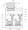
In this embodiment, an example of a process for manufacturing an inverter circuit will be described as an example of a semiconductor device using a CMOS circuit. Note that the present invention is not limited to such a simple circuit, and various integrated circuits including a microprocessor can be realized. 7A to 13A are top views of the inverter circuit, and FIG. 7B is a cross-sectional view corresponding to the line AB.
図4にしめされた単結晶半導体層306が絶縁膜417を介して絶縁基板305上に形成されているSOI基板を用いて半導体装置を作製する。また、実施例2の図6(B)に示した半導体基板212を単結晶半導体層の形成に利用してもよい。まず、単結晶半導体層306をエッチングにより島状に加工し、{110}面を有する第1の半導体層306aから第1の活性層400aを、{100}面を有する第2の半導体層306bから第2の活性層400bを複数個形成する。第1の活性層400aはP導電型TFTのチャネル形成領域に、第2の活性層400bはN導電型TFTのチャネル形成領域に用いる。このとき、単結晶半導体層306と同時に絶縁膜417もエッチングしてもよい。なお、絶縁膜417は、酸化窒化珪素膜301、窒化酸化珪素膜302及び接合層304の積層絶縁膜である。
A semiconductor device is manufactured using an SOI substrate in which the single
図7(A)及び(B)は、島状に加工された第1の活性層400a及び第2の活性層400bが設けられた絶縁基板305にゲート絶縁層及びゲート電極を形成する工程を示している。第1の活性層400a及び第2の活性層400b上には、ゲート絶縁層401を介して、ゲート電極層402が設けられる。ゲート絶縁層401としては、酸化珪素(SiOx)、酸化窒化珪素(SiOxNy)、酸化ハフニウム(HfOx)、酸化アルミニウム(AlxOy)(x>y>0)、酸化タンタル(TaxOy、x>y>0)などの材料を適用することができる。図7(B)では、ゲート絶縁層401とゲート電極層402の側端部が揃うように加工されているが、ゲート電極層402のエッチングにおいてゲート絶縁層401を残すように加工してもよい。例えば、ゲート絶縁層401をテーパ状に残すような加工をしてもよい。
7A and 7B show a process of forming a gate insulating layer and a gate electrode over the insulating
ゲート電極層402は単層構造であっても、積層構造であってもよい。本実施の形態では、第1のゲート電極層403、第2のゲート電極層404の積層構造の場合を示す。ゲート絶縁層401に高誘電率物質(high−k材料)を用いる場合には、ゲート電極層402を多結晶シリコン、シリサイド、金属若しくは金属窒化物で形成し、好適には金属若しくは金属窒化物で形成することが望ましい。ゲート電極層が積層構造であることを考慮すると、ゲート絶縁層401と接する第1のゲート電極層403を金属窒化物材料で形成し、第2のゲート電極層404を金属材料で形成することができる。この組み合わせを用いることによって、ゲート絶縁層が薄膜化した場合でもゲート電極に空乏層が広がってしまうことを積極的に防止でき、微細化した場合にもトランジスタの駆動能力を損なうことを防止することができる。
The
図8はゲート電極層402上に第1の絶縁層405を形成する工程を示している。第1の絶縁層405として、酸化珪素膜若しくは酸化窒化珪素膜をCVD法やスパッタ法により形成する。他の形態として、ゲート電極層402を酸化又は窒化処理により絶縁化して同様の層を形成してもよい。第1の絶縁層405はゲート電極層402の側壁にも1nm乃至10nmの厚さで形成されるようにする。第1の絶縁層405は、第1の活性層400a及び第2の活性層400bに対し、価電子制御を目的とした不純物が添加されないオフセット領域を形成するためにも設けている。
FIG. 8 shows a step of forming the first insulating
図9は、第1の活性層400a及び第2の活性層400bに極浅不純物領域(ソースドレインエクステンション)を形成する工程を示している。この極浅不純物領域によって、短チャネル効果を抑制することができる。P導電型TFTの第1の活性層400aに対しては第13族元素が添加される第1の極浅不純物領域406を形成し、N導電型TFTの第2の活性層400bに対しては第15族元素が添加される第2の極浅不純物領域407を形成する。なお図9(A)において、極浅不純物領域406、407を分かりやすく示すため、ゲート電極層402周囲の第1の絶縁層405のみを示し、第1の絶縁層405の外側に極浅不純物領域406、407を点線で示すが、第1の絶縁層405は、第1の活性層400a、第2の活性層400b、ゲート電極層402の全体を覆っている。この極浅不純物領域の不純物濃度は、例えば、第1の極浅不純物領域406については、硼素を15keV、3×10¹³/cm2のドーズ量でイオン注入を行い、第2の極浅不純物領域407については、砒素を15keV、2×1014/cm2のドーズ量でイオン注入を行う。
FIG. 9 shows a process of forming an extremely shallow impurity region (source / drain extension) in the first
次いで、図10で示すように、ゲート電極層402の側面に第1のサイドウオール408、第2のサイドウオール409を形成する。例えば、第1のサイドウオール408、第2のサイドウオール409は窒化珪素膜で形成される。これらのサイドウオールは異方性エッチングにより自己整合的に形成する。
Next, as illustrated in FIG. 10, a
この場合、第1の活性層400a側の第1のサイドウオール408と、第2の活性層400b側の第2のサイドウオール409の幅を同じとなるように加工しても良いが、好ましくはこの両者の幅が異なるように加工する。P導電型TFTである第1の活性層400aに対する第1のサイドウオール408の幅は、N導電型TFTである第2の活性層400bに対する第2のサイドウオール409の幅よりも厚くするとよい。P導電型TFTにおいてソース領域及びドレイン領域を形成するために注入される硼素は拡散しやすく、短チャネル効果を誘起しやすいためである。むしろ、このような構成とすることで、P導電型TFTにおいて、ソース領域及びドレイン領域に高濃度の硼素を添加することが可能となり、ソース領域及びドレイン領域を低抵抗化することができる。
In this case, the
サイドウオールを形成した後、図11で示すように、第1の絶縁層405の露出部をエッチングした後、ソース領域及びドレイン領域を自己整合的に形成する。この工程は、価電子制御する不純物イオンを電界で加速して注入するイオン注入法で行うことができる。図11(B)には、第1の活性層400aには第13族元素を添加して、ソース領域及びドレイン領域となる第1の不純物領域410を形成する状態を示す。また第2の活性層400bには第15族元素を添加して、ソース領域及びドレイン領域となる第2の不純物領域411を形成する。例えば、P導電型TFTの第1の活性層400aについては、硼素を30keV、3×10¹⁵/cm2のドーズ量でイオン注入する。N導電型TFTの第2の活性層400bについては、砒素を50keV、5×1015/cm2のドーズ量でイオン注入する。上記のイオン種、加速電圧及びドーズ量のドーピング条件は例示であって、適宜設定した条件とすることもできる。
After the sidewall is formed, as shown in FIG. 11, the exposed portion of the first insulating
ソース領域及びドレイン領域をさらに低抵抗化するには、第1及び第2の活性層に対して、シリサイド層を形成してもよい。シリサイド層としては、コバルトシリサイド若しくはニッケルシリサイドを適用すればよく、少なくともソース領域及びドレイン領域をシリサイド化すればよく、活性層の上面及び端面に対してシリサイド層を形成することとなる。なお、上記活性層の厚さが薄い場合等には、活性層の底部までシリサイド反応を進めて、低抵抗化を図ってもよい。また、ゲート電極層402に多結晶シリコンを用いている場合には、ゲート電極層402をさらに低抵抗化するためにも、第1の絶縁層405をエッチングしてゲート電極層の上面にシリサイド層を形成するとよい。ソース領域及びドレイン領域に対するシリサイド層と、ゲート電極層に対するシリサイド層とは同時に作製することができる。
In order to further reduce the resistance of the source region and the drain region, a silicide layer may be formed for the first and second active layers. As the silicide layer, cobalt silicide or nickel silicide may be applied, and at least the source region and the drain region may be silicided, and the silicide layer is formed on the upper surface and the end surface of the active layer. If the active layer is thin, the silicide reaction may be advanced to the bottom of the active layer to reduce the resistance. In the case where polycrystalline silicon is used for the
図12では、パッシベーション層412、第1の層間絶縁層413、コンタクトプラグ414を形成する工程を示す。パッシベーション層412は窒化珪素膜、窒化酸化珪素膜などをCVD法で全面に成膜する。第1の層間絶縁層413は、リンシリケートガラス(PSG)若しくはボロンリンシリケートガラス(BPSG)をCVD法で成膜し、リフローにより平坦化して形成する。または、CVD法でテトラエトキシシラン(Tetra−Ethyl−Ortho−Silicate、 Si(OCH2CH3)4)を用いて酸化珪素膜を形成し、その後CMPで平坦化してもよい。コンタクトプラグ414は、第1の層間絶縁層413に形成したコンタクトホールを埋め込むようにタングステンシリサイドで形成する。タングステンシリサイドは六フッ化タングステン(WF6)とシラン(SiH4)を用いてCVD法で形成する。
FIG. 12 shows a step of forming a
配線の多層化は、半導体素子及び該素子を用いた装置の構成に応じて考慮される。図13では、第1の層間絶縁層413の上に、第2の層間絶縁層415と配線416を設けた構成を示している。配線はタングステンシリサイドで形成しても良いし、ダマシン法によりCu配線を設けてもよい。
Multi-layered wiring is considered according to the configuration of a semiconductor element and a device using the element. FIG. 13 illustrates a structure in which a second
(実施の形態4)
本実施の形態は、半導体素子を有する装置(半導体装置)の一例としてマイクロプロセッサの態様について図14を参照して説明する。
(Embodiment 4)
In this embodiment, an example of a microprocessor will be described with reference to FIG. 14 as an example of a device having a semiconductor element (semiconductor device).
図14はマイクロプロセッサ501の一例を示す。このマイクロプロセッサ501では、N導電型TFTを構成する活性層と、P導電型TFTを構成する活性層の結晶面方位が異なっている。
FIG. 14 shows an example of the
このマイクロプロセッサ501は、演算回路502(Arithmetic logic unit。ALUともいう。)、演算回路制御部503(ALU Controller)、命令解析部504(Instruction Decoder)、割り込み制御部505(Interrupt Controller)、タイミング制御部506(Timing Controller)、レジスタ507(Register)、レジスタ制御部508(Register Controller)、バスインターフェース509(Bus I/F)、読み出し専用メモリ510、及びROMインターフェース511(ROM I/F)を有している。
The
バスインターフェース509を介してマイクロプロセッサ501に入力された命令は、命令解析部504に入力されてデコードされた後、演算回路制御部503、割り込み制御部505、レジスタ制御部508、タイミング制御部506に入力される。演算回路制御部503、割り込み制御部505、レジスタ制御部508、タイミング制御部506は、デコードされた命令に基づき、各種制御を行う。具体的に演算回路制御部503は、演算回路502の動作を制御するための信号を生成する。また、割り込み制御部505は、マイクロプロセッサ501のプログラム実行中に、外部の入出力装置や、周辺回路からの割り込み要求を、その優先度やマスク状態から判断し、処理する。レジスタ制御部508は、レジスタ507のアドレスを生成し、マイクロプロセッサの状態に応じてレジスタ507の読み出しや書き込みを行う。
An instruction input to the
またタイミング制御部506は、演算回路502、演算回路制御部503、命令解析部504、割り込み制御部505、レジスタ制御部508の動作のタイミングを制御する信号を生成する。例えばタイミング制御部506は、基準クロック信号CLK1を元に、内部クロック信号CLK2を生成する内部クロック生成部を備えており、クロック信号CLK2を上記各種回路に供給する。なお、図14に示すマイクロプロセッサ501は、その構成を簡略化して示した一例にすぎず、実際のCPUはその用途によって多種多様な構成を有している。
The
本実施の形態のマイクロプロセッサは、P導電型TFTの第1の活性層とN導電型TFTに供する第2の活性層が、絶縁基板の同一面に設けられ、かつ、その両者の結晶面方位が異なっている。このように、TFTのチャネルを流れるキャリアにとって移動度が高くなる結晶面を適用することにより、マイクロプロセッサの動作の高速化を図ることができる。また、低電圧で駆動することが可能となり、低消費電力化を図ることができる。すなわち、キャリアが原子で散乱される確率を低減することができ、それによって電子又はホールの受ける抵抗を減少させ、マイクロプロセッサの性能向上を図ることができる。 In the microprocessor according to the present embodiment, the first active layer of the P-conductivity type TFT and the second active layer provided for the N-conductivity type TFT are provided on the same surface of the insulating substrate, and the crystal plane orientations of the both are provided. Is different. In this manner, the operation of the microprocessor can be speeded up by applying a crystal plane whose mobility is high for carriers flowing through the channel of the TFT. In addition, it is possible to drive at a low voltage, so that power consumption can be reduced. That is, the probability that carriers are scattered by atoms can be reduced, whereby the resistance received by electrons or holes can be reduced, and the performance of the microprocessor can be improved.
(実施の形態5)
本実施の形態は、半導体素子を有する装置の一例として通信回路を有し非接触でデータの入出力が可能なマイクロコンピュータの態様について図15を参照して説明する。
(Embodiment 5)
In this embodiment, an example of a microcomputer that includes a communication circuit and can input and output data without contact will be described with reference to FIG. 15 as an example of a device having a semiconductor element.
図15は本実施の形態に係るマイクロコンピュータ512のブロック図を示している。このマイクロコンピュータ512は、アンテナ回路513、アナログ回路部514及びデジタル回路部515を有している。アナログ回路部514として、共振容量を有する共振回路516、定電圧回路517、整流回路518、復調回路519と、変調回路520、リセット回路521、発振回路522、電源管理回路523を有している。デジタル回路部515は、RFインターフェース524、制御レジスタ525、クロックコントローラ526、インターフェース527、中央処理ユニット528、ランダムアクセスメモリ529、読み出し専用メモリ530を有している。また、マイクロコンピュータ512の動作に必要な電力は、無線信号をアンテナ回路513が受信したものを、整流回路518を経て整流された電力が蓄電部531に充電される。蓄電部531はセラミックコンデンサーや電気二重層コンデンサーなどのキャパシタで構成される。蓄電部531はマイクロコンピュータ512と一体形成されている必要はなく、別部品としてマイクロコンピュータ512を構成する絶縁表面を有する基板に取り付けられていれば良い。
FIG. 15 is a block diagram of the
このような構成のマイクロコンピュータ512の動作は以下の通りである。アンテナ回路513が受信した信号は共振回路516により誘導起電力を生じる。入力された信号は、復調回路519で復調され、制御命令やデータ信号がデジタル回路部515に出力される。リセット回路521は、デジタル回路部515をリセットし初期化する信号を生成する。例えば、電源電圧の上昇に遅延して立ち上がる信号をリセット信号として生成する。発振回路522は、定電圧回路517により生成される制御信号に応じて、クロック信号の周波数とデューティー比を変更する。ローパスフィルタで形成される復調回路519は、例えば振幅変調(ASK)方式の受信信号の振幅の変動を二値化する。変調回路520は、送信データを振幅変調(ASK)方式の送信信号の振幅を変動させて送信する。変調回路520は、共振回路516の共振点を変化させることで通信信号の振幅を変化させている。クロックコントローラ526は、電源電圧又は中央処理ユニット528における消費電流に応じてクロック信号の周波数とデューティー比を変更するための制御信号を生成している。電源電圧の監視は電源管理回路523が行っている。
The operation of the
アンテナ回路513からマイクロコンピュータ512に入力された信号は復調回路519で復調された後、RFインターフェース524で制御コマンドやデータなどに分解される。制御コマンドは制御レジスタ525に格納される。制御コマンドには読み出し専用メモリ530に記憶されているデータの読み出し、ランダムアクセスメモリ529へのデータの書き込み、中央処理ユニット528への演算命令などが含まれている。中央処理ユニット528は、インターフェース527を介して読み出し専用メモリ530、ランダムアクセスメモリ529、制御レジスタ525にアクセスする。インターフェース527は、中央処理ユニット528が要求するアドレスより、読み出し専用メモリ530、ランダムアクセスメモリ529、制御レジスタ525のいずれかに対するアクセス信号を生成する機能を有している。
A signal input from the
中央処理ユニット528の演算方式は、読み出し専用メモリ530にOS(オペレーティングシステム)を記憶させておいて、起動とともにプログラムを読み出し実行する方式を採用することができる。また、専用回路で演算回路を構成して、演算処理をハードウェア的に処理する方式を採用することもできる。ハードウェアとソフトウェアを併用する方式では、専用の演算回路で一部の処理を行い、残りの演算をプログラムを使って中央処理ユニット528が実行する方式を適用することができる。
As a calculation method of the central processing unit 528, a method in which an OS (operating system) is stored in the read-
図16は、上記のような構成を有する本実施の形態に係るマイクロコンピュータの外観を示す。絶縁基板305に複数の活性層が設けられ、それによりN導電型TFT及びP導電型TFTが形成される素子形成層532を有している。素子形成層532は、図15におけるアナログ回路部514及びデジタル回路部515を形成する。アンテナ533は絶縁基板305上に設けられている。また、このアンテナ533に替えてアンテナ接続端子を設けても良い。図16で示すアンテナ533は磁界型のスパイラルアンテナを示すが、電界型のアンテナとしてダイポールアンテナなどと組み合わせても良い。
FIG. 16 shows the appearance of the microcomputer according to the present embodiment having the above-described configuration. The insulating
図17は、図16で示すマイクロコンピュータの要部を示し、断面構造を模式的に示している。絶縁基板305上には第1の活性層400a及び第2の活性層400bによってP導電型TFT及びN導電型TFTが形成されている。第2の層間絶縁層415よりも下層の構成は図13と同様であるので省略する。
FIG. 17 shows a main part of the microcomputer shown in FIG. 16 and schematically shows a cross-sectional structure. A P-conductivity type TFT and an N-conductivity type TFT are formed on the insulating
第1の配線416上には第3の層間絶縁層534、第4の層間絶縁層535が形成されている。第3の層間絶縁層534は酸化珪素膜、第4の層間絶縁層535は窒化珪素膜で形成し、デュアルダマシンにより、第3の層間絶縁層534に形成される開口部は、第4の層間絶縁層535に形成される開口部より狭くなっている。その開口部に窒化タンタルなどのバリアメタル536を形成し、銅メッキにより銅配線537を形成している。さらに第5の層間絶縁層538、第6の層間絶縁層539を形成し、第6の層間絶縁層539に対してのみ開口部を形成し、該開口部にバリアメタル540及び銅メッキによる銅配線541を設ける。銅配線541上には、第7の層間絶縁層542が形成されており、アンテナ533を銅配線541に接続するための開口部を形成する。そして、アンテナ533を第7の層間絶縁層542上に設け、銅配線541と接続させる。図17では、アンテナ533と銅配線541との境界にシード層543を形成するが、該シード層はアンテナ533を銅メッキ法で形成する場合に設けられる。アンテナ533はインクジェット法や印刷法等により直接描画することもでき、スパッタリングによりアルミニウムなどの導電膜を堆積し、それをフォトリソグラフィー法でアンテナ形状に加工してもよい。
A third
このようなマイクロコンピュータは、絶縁基板305として大面積のガラス基板を用いることによって生産性を向上させることができる。例えば、市場に流通している第4世代の液晶パネルには730mm×920mmのガラス基板が採用されており、面積は671600mm2である。このようなガラス基板からマイクロコンピュータを取り出す場合、チップの切しろの分を無視したとしても、2mm角で切り出す場合には概算でも34万個を取り出すことができる。ガラス基板の厚さは0.4〜0.7mmであり、TFTの活性層を固定する面と反対側の面に保護フィルムを貼れば、装置全体として0.1〜0.3mm程度まで薄くすることも可能である。
Such a microcomputer can improve productivity by using a large-area glass substrate as the insulating
本実施の形態のマイクロコンピュータは、P導電型TFTの第1の活性層とN導電型TFTに供する第2の活性層が、絶縁基板の同一面に設けられ、かつ、その両者の結晶面方位が異なっている。このように、TFTのチャネルを流れるキャリアにとって移動度が高くなる結晶面を適用することにより、マイクロコンピュータの動作の高速化を図ることができる。また、低電圧で駆動することが可能となり、低消費電力化を図ることができる。すなわち、キャリアが原子で散乱される確率を低減することができ、それによって電子又はホールの受ける抵抗を減少させ、マイクロコンピュータの性能向上を図ることができる。 In the microcomputer of this embodiment, the first active layer of the P-conductivity type TFT and the second active layer used for the N-conductivity type TFT are provided on the same surface of the insulating substrate, and the crystal plane orientations of both Is different. In this manner, the operation of the microcomputer can be speeded up by applying a crystal plane whose mobility is high for carriers flowing in the TFT channel. In addition, it is possible to drive at a low voltage, so that power consumption can be reduced. That is, the probability that carriers are scattered by atoms can be reduced, whereby the resistance received by electrons or holes can be reduced, and the performance of the microcomputer can be improved.
(実施の形態6)
本実施の形態では、同一表面上に二つの異なる結晶面方位を有する半導体基板202を用いたCMOSトランジスタについて説明する。
(Embodiment 6)
In this embodiment, a CMOS transistor using a
図18は半導体基板202を用いて形成したCMOSトランジスタの一例である。第1の活性層400a、第2の活性層400b、絶縁領域701、不純物領域702及び703、ゲート絶縁層704、ゲート電極層705、第1の絶縁層706、第2の絶縁層707、配線708等により構成される。P電型トランジスタが形成される第1の活性層400aとN導電型トランジスタが形成される第2の活性層400bは互いに結晶面方位が異なっており、それぞれのチャネルを流れるキャリアにとって移動度が高くなる結晶面を適用している。また、N導電型トランジスタとP導電型トランジスタは絶縁領域701の存在により完全に分離されている。
FIG. 18 illustrates an example of a CMOS transistor formed using the
図19は従来の半導体基板を用いて形成したCMOSトランジスタの一例である。N導電型基板809、P導電型のウェル810、不純物領域802及び803、ゲート絶縁層804、ゲート電極層805、第1の絶縁層806、第2の絶縁層807、配線808等により構成される。N導電型トランジスタとP導電型トランジスタの活性層は同一の結晶面方位を有している。また、従来のCOMSトランジスタでは、N導電型トランジスタとP導電型トランジスタが電気的に完全に分離されていないため、基板内部にPNPNという寄生サイリスタ構造が形成される。これにより、入力電圧が電源電圧の範囲を超えて入力されるとラッチアップが発生する。ラッチアップはCMOSトランジスタ特有の不良モードである。
FIG. 19 shows an example of a CMOS transistor formed using a conventional semiconductor substrate. An N
本実施の形態のCMOSトランジスタは、N導電型トランジスタの活性層とP導電型トランジスタの活性層をそれぞれのチャネルを流れるキャリアにとって移動度が高くなる結晶面方位を適用することにより、動作の高速化を図ることができる。また、低電圧で駆動することが可能となり、低消費電力化を図ることができる。また、本実施の形態のCMOSトランジスタでは絶縁領域701の存在により、ウェルを形成する必要がなく工程の簡略化が可能であり、基板内部に寄生サイリスタ構造を有しないため、ラッチアップの抑制を図ることができる。
In the CMOS transistor of this embodiment, the operation speed is increased by applying a crystal plane orientation in which the mobility for carriers flowing through the respective channels is applied to the active layer of the N-conductivity type transistor and the active layer of the P-conductivity type transistor. Can be achieved. In addition, it is possible to drive at a low voltage, so that power consumption can be reduced. Further, in the CMOS transistor of this embodiment, due to the presence of the
101 第1の半導体基板
102 第2の半導体基板
103 酸化珪素膜
104 酸化珪素膜
111 第1の半導体基板
112 第2の半導体基板
201 半導体インゴット
202 半導体基板
203 イオンビーム
211 半導体インゴット
212 半導体基板
301 酸化窒化珪素膜
302 窒化酸化珪素膜
303 脆化層
304 接合層
305 絶縁基板
306 単結晶半導体層
306a 第1の半導体層
306b 第2の半導体層
307a P導電型TFTのチャネル長方向
307b N導電型TFTのチャネル長方向
101
Claims (6)
基板側面の結晶面方位が、前記第1の結晶面方位と異なる第2の結晶面方位である第2の半導体基板の表面に絶縁膜を形成し、
前記第1の半導体基板と前記第2の半導体基板とを前記絶縁膜を介して交互に複数枚接合することにより半導体インゴットを形成し、
前記半導体インゴットを、前記第1の結晶面方位を有する第1の半導体層と、前記第2の結晶面方位を有する第2の半導体層とが、交互に配置される面と平行にスライスし、
前記第1の半導体層と、前記第2の半導体層とが、交互に配置された半導体基板を形成し、
前記半導体基板にイオンビームを照射し、前記半導体基板中に脆化層を形成し、
前記半導体基板と、絶縁基板とを重ね合わせ、
前記半導体基板と、前記絶縁基板とを重ね合わせた状態で熱処理を行って、前記脆化層に亀裂を生じさせ、前記半導体基板から単結晶半導体層を分離させ、
前記絶縁基板上に前記第1の半導体層と、前記第2の半導体層とが交互に配置された該単結晶半導体層を形成し、
前記第1の半導体層に、それぞれチャネル形成領域を有する複数個の第1の薄膜トランジスタを形成し、
前記第2の半導体層に、それぞれチャネル形成領域を有する複数個の第2の薄膜トランジスタを形成することを特徴とする半導体装置の作製方法。 Forming an insulating film on the surface of the first semiconductor substrate in which the crystal plane orientation of the substrate side surface is the first crystal plane orientation;
Forming an insulating film on the surface of the second semiconductor substrate in which the crystal plane orientation of the substrate side surface is a second crystal plane orientation different from the first crystal plane orientation;
Forming a semiconductor ingot by alternately bonding a plurality of the first semiconductor substrate and the second semiconductor substrate via the insulating film;
Slicing the semiconductor ingot in parallel with the plane in which the first semiconductor layer having the first crystal plane orientation and the second semiconductor layer having the second crystal plane orientation are alternately arranged,
Forming a semiconductor substrate in which the first semiconductor layer and the second semiconductor layer are alternately arranged;
Irradiating the semiconductor substrate with an ion beam, forming an embrittlement layer in the semiconductor substrate,
The semiconductor substrate and the insulating substrate are overlaid,
Heat treatment is performed in a state where the semiconductor substrate and the insulating substrate are overlapped to cause a crack in the embrittlement layer, and a single crystal semiconductor layer is separated from the semiconductor substrate,
Forming the single crystal semiconductor layer in which the first semiconductor layer and the second semiconductor layer are alternately arranged on the insulating substrate;
Forming a plurality of first thin film transistors each having a channel formation region in the first semiconductor layer;
A method for manufacturing a semiconductor device, comprising: forming a plurality of second thin film transistors each having a channel formation region in the second semiconductor layer.
前記第1の結晶面方位は、{100}であって、
前記第2の結晶面方位は、{110}であることを特徴とする半導体装置の作製方法。 In claim 1 ,
The first crystal plane orientation is {100},
The method for manufacturing a semiconductor device, wherein the second crystal plane orientation is {110}.
前記第1の薄膜トランジスタは、チャネル長方向の結晶軸が<100>となるように形成されたN導電型薄膜トランジスタであって、
前記第2の薄膜トランジスタは、チャネル長方向の結晶軸が<110>となるように形成されたP導電型薄膜トランジスタであることを特徴とする半導体装置の作製方法。 The first thin film transistor according to claim 1 or 2 , wherein the first thin film transistor is an N-conductivity thin film transistor formed so that a crystal axis in a channel length direction is <100>.
The method for manufacturing a semiconductor device, wherein the second thin film transistor is a P-conductivity thin film transistor formed so that a crystal axis in a channel length direction is <110>.
基板側面の結晶面方位が、前記第1の結晶面方位と異なる第2の結晶面方位である第2の半導体基板の表面に絶縁膜を形成し、
前記第1の半導体基板と、前記第2の半導体基板とを前記絶縁膜を介して交互に複数枚接合することにより半導体インゴットを形成し、
前記半導体インゴットにおいて、前記第1の結晶面方位を有する第1の半導体層と、前記第2の結晶面方位を有する第2の半導体層とが、交互に配置される面と平行にスライスすることを特徴とする半導体基板の作製方法。 Forming an insulating film on the surface of the first semiconductor substrate in which the crystal plane orientation of the substrate side surface is the first crystal plane orientation;
Forming an insulating film on the surface of the second semiconductor substrate in which the crystal plane orientation of the substrate side surface is a second crystal plane orientation different from the first crystal plane orientation;
Forming a semiconductor ingot by alternately joining a plurality of the first semiconductor substrate and the second semiconductor substrate via the insulating film;
In the semiconductor ingot, the first semiconductor layer having the first crystal plane orientation and the second semiconductor layer having the second crystal plane orientation are sliced in parallel with the alternately arranged planes. A manufacturing method of a semiconductor substrate characterized by the above.
前記第1の半導体基板の側面の結晶面方位は、{100}であって、
前記第2の半導体基板の側面の結晶面方位は、{110}であることを特徴とする半導体基板の作製方法。 In claim 4 ,
The crystal plane orientation of the side surface of the first semiconductor substrate is {100},
A method for manufacturing a semiconductor substrate, wherein a crystal plane orientation of a side surface of the second semiconductor substrate is {110}.
前記第1の半導体基板は、P導電型であって、
前記第2の半導体基板は、N導電型であることを特徴とする半導体基板の作製方法。 In claim 4 or claim 5 ,
The first semiconductor substrate is of P conductivity type,
The method for manufacturing a semiconductor substrate, wherein the second semiconductor substrate is of N conductivity type.
Priority Applications (1)
| Application Number | Priority Date | Filing Date | Title |
|---|---|---|---|
| JP2008291094A JP5394043B2 (en) | 2007-11-19 | 2008-11-13 | Semiconductor substrate, semiconductor device using the same, and manufacturing method thereof |
Applications Claiming Priority (3)
| Application Number | Priority Date | Filing Date | Title |
|---|---|---|---|
| JP2007298799 | 2007-11-19 | ||
| JP2007298799 | 2007-11-19 | ||
| JP2008291094A JP5394043B2 (en) | 2007-11-19 | 2008-11-13 | Semiconductor substrate, semiconductor device using the same, and manufacturing method thereof |
Publications (3)
| Publication Number | Publication Date |
|---|---|
| JP2009147313A JP2009147313A (en) | 2009-07-02 |
| JP2009147313A5 JP2009147313A5 (en) | 2011-11-24 |
| JP5394043B2 true JP5394043B2 (en) | 2014-01-22 |
Family
ID=40640958
Family Applications (1)
| Application Number | Title | Priority Date | Filing Date |
|---|---|---|---|
| JP2008291094A Expired - Fee Related JP5394043B2 (en) | 2007-11-19 | 2008-11-13 | Semiconductor substrate, semiconductor device using the same, and manufacturing method thereof |
Country Status (2)
| Country | Link |
|---|---|
| US (2) | US7879689B2 (en) |
| JP (1) | JP5394043B2 (en) |
Families Citing this family (5)
| Publication number | Priority date | Publication date | Assignee | Title |
|---|---|---|---|---|
| US20100176495A1 (en) * | 2009-01-12 | 2010-07-15 | International Business Machines Corporation | Low cost fabrication of double box back gate silicon-on-insulator wafers |
| US7767546B1 (en) * | 2009-01-12 | 2010-08-03 | International Business Machines Corporation | Low cost fabrication of double box back gate silicon-on-insulator wafers with built-in shallow trench isolation in back gate layer |
| US20100176482A1 (en) | 2009-01-12 | 2010-07-15 | International Business Machine Corporation | Low cost fabrication of double box back gate silicon-on-insulator wafers with subsequent self aligned shallow trench isolation |
| US8587063B2 (en) * | 2009-11-06 | 2013-11-19 | International Business Machines Corporation | Hybrid double box back gate silicon-on-insulator wafers with enhanced mobility channels |
| US11521972B2 (en) | 2020-05-01 | 2022-12-06 | Tokyo Electron Limited | High performance multi-dimensional device and logic integration |
Family Cites Families (27)
| Publication number | Priority date | Publication date | Assignee | Title |
|---|---|---|---|---|
| JPH01162376A (en) * | 1987-12-18 | 1989-06-26 | Fujitsu Ltd | Manufacture of semiconductor device |
| JPH07101679B2 (en) * | 1988-11-01 | 1995-11-01 | 三菱電機株式会社 | Wafer for electronic device, rod-shaped substrate for wafer, and electronic device |
| JPH0590117A (en) | 1991-09-27 | 1993-04-09 | Toshiba Corp | Single crystal thin film semiconductor device |
| JPH07297377A (en) | 1994-04-21 | 1995-11-10 | Mitsubishi Electric Corp | Semiconductor device and manufacture thereof |
| JPH11163363A (en) | 1997-11-22 | 1999-06-18 | Semiconductor Energy Lab Co Ltd | Semiconductor device and its forming method |
| JP2000012864A (en) * | 1998-06-22 | 2000-01-14 | Semiconductor Energy Lab Co Ltd | Manufacture of semiconductor device |
| JP3432187B2 (en) * | 1999-09-22 | 2003-08-04 | シャープ株式会社 | Method for manufacturing semiconductor device |
| US20020031909A1 (en) * | 2000-05-11 | 2002-03-14 | Cyril Cabral | Self-aligned silicone process for low resistivity contacts to thin film silicon-on-insulator mosfets |
| US6583440B2 (en) * | 2000-11-30 | 2003-06-24 | Seiko Epson Corporation | Soi substrate, element substrate, semiconductor device, electro-optical apparatus, electronic equipment, method of manufacturing the soi substrate, method of manufacturing the element substrate, and method of manufacturing the electro-optical apparatus |
| CN100403543C (en) * | 2001-12-04 | 2008-07-16 | 信越半导体株式会社 | Pasted wafer and method for producing pasted wafer |
| US6908797B2 (en) * | 2002-07-09 | 2005-06-21 | Semiconductor Energy Laboratory Co., Ltd. | Method of manufacturing a semiconductor device |
| US6818529B2 (en) * | 2002-09-12 | 2004-11-16 | Applied Materials, Inc. | Apparatus and method for forming a silicon film across the surface of a glass substrate |
| JP3927165B2 (en) | 2003-07-03 | 2007-06-06 | 株式会社東芝 | Semiconductor device |
| US6821826B1 (en) * | 2003-09-30 | 2004-11-23 | International Business Machines Corporation | Three dimensional CMOS integrated circuits having device layers built on different crystal oriented wafers |
| US20050275018A1 (en) * | 2004-06-10 | 2005-12-15 | Suresh Venkatesan | Semiconductor device with multiple semiconductor layers |
| DE102004031708B4 (en) * | 2004-06-30 | 2008-02-07 | Advanced Micro Devices, Inc., Sunnyvale | Method for producing a substrate with crystalline semiconductor regions of different properties |
| JP2006040911A (en) * | 2004-07-22 | 2006-02-09 | Renesas Technology Corp | Semiconductor device and its manufacturing method |
| US7312487B2 (en) * | 2004-08-16 | 2007-12-25 | International Business Machines Corporation | Three dimensional integrated circuit |
| US7235433B2 (en) * | 2004-11-01 | 2007-06-26 | Advanced Micro Devices, Inc. | Silicon-on-insulator semiconductor device with silicon layers having different crystal orientations and method of forming the silicon-on-insulator semiconductor device |
| US7298009B2 (en) * | 2005-02-01 | 2007-11-20 | Infineon Technologies Ag | Semiconductor method and device with mixed orientation substrate |
| US7372720B1 (en) * | 2005-02-16 | 2008-05-13 | Altera Corporation | Methods and apparatus for decreasing soft errors and cell leakage in integrated circuit structures |
| US7432149B2 (en) * | 2005-06-23 | 2008-10-07 | Taiwan Semiconductor Manufacturing Company, Ltd. | CMOS on SOI substrates with hybrid crystal orientations |
| US7709317B2 (en) * | 2005-11-14 | 2010-05-04 | International Business Machines Corporation | Method to increase strain enhancement with spacerless FET and dual liner process |
| US7288458B2 (en) * | 2005-12-14 | 2007-10-30 | Freescale Semiconductor, Inc. | SOI active layer with different surface orientation |
| EP1993130A3 (en) * | 2007-05-17 | 2011-09-07 | Semiconductor Energy Laboratory Co., Ltd. | Semiconductor device and method for manufacturing the same |
| JP2009076879A (en) * | 2007-08-24 | 2009-04-09 | Semiconductor Energy Lab Co Ltd | Semiconductor device |
| US8232598B2 (en) * | 2007-09-20 | 2012-07-31 | Semiconductor Energy Laboratory Co., Ltd. | Display device and method for manufacturing the same |
-
2008
- 2008-11-13 JP JP2008291094A patent/JP5394043B2/en not_active Expired - Fee Related
- 2008-11-18 US US12/273,010 patent/US7879689B2/en not_active Expired - Fee Related
-
2011
- 2011-01-25 US US13/013,063 patent/US8653568B2/en not_active Expired - Fee Related
Also Published As
| Publication number | Publication date |
|---|---|
| US8653568B2 (en) | 2014-02-18 |
| US20110114998A1 (en) | 2011-05-19 |
| US7879689B2 (en) | 2011-02-01 |
| US20090127591A1 (en) | 2009-05-21 |
| JP2009147313A (en) | 2009-07-02 |
Similar Documents
| Publication | Publication Date | Title |
|---|---|---|
| JP5364281B2 (en) | Method for manufacturing semiconductor device | |
| JP5354952B2 (en) | Semiconductor device | |
| KR102330115B1 (en) | Method for forming a semiconductor-on-insulator(soi) substrate | |
| TWI395295B (en) | Integrated circuit and method for its manufacture | |
| JP2012169640A (en) | Semiconductor device | |
| TWI588993B (en) | Semiconductor component and method for fabricating the same | |
| JP5394043B2 (en) | Semiconductor substrate, semiconductor device using the same, and manufacturing method thereof | |
| US20200098618A1 (en) | Semiconductor-on-insulator (soi) substrate, method for forming thereof, and integrated circuit | |
| US8501585B2 (en) | Manufacturing method of semiconductor device | |
| US6229179B1 (en) | Intelligent power integrated circuit | |
| US20090302482A1 (en) | Structure and Method for Forming Hybrid Substrate | |
| TW200826230A (en) | Semiconductor device and method for manufacturing the same | |
| US9583397B1 (en) | Source/drain terminal contact and method of forming same | |
| US11923237B2 (en) | Manufacturing method of semiconductor device | |
| US20230015572A1 (en) | Liner layer for backside contacts of semiconductor devices | |
| TW202238837A (en) | Method for fabricating semiconductor device | |
| JP2002009015A (en) | Semiconductor device and its manufacturing method | |
| JP2004207528A (en) | Semiconductor device and its manufacturing method | |
| JP2004273589A (en) | Semiconductor device and its fabricating process | |
| JP2004207529A (en) | Semiconductor device and its manufacturing method | |
| JP2001257274A (en) | Semiconductor device and its manufacturing method |
Legal Events
| Date | Code | Title | Description |
|---|---|---|---|
| RD02 | Notification of acceptance of power of attorney |
Free format text: JAPANESE INTERMEDIATE CODE: A7422 Effective date: 20110914 |
|
| A521 | Request for written amendment filed |
Free format text: JAPANESE INTERMEDIATE CODE: A523 Effective date: 20111012 |
|
| A621 | Written request for application examination |
Free format text: JAPANESE INTERMEDIATE CODE: A621 Effective date: 20111012 |
|
| A977 | Report on retrieval |
Free format text: JAPANESE INTERMEDIATE CODE: A971007 Effective date: 20130718 |
|
| A131 | Notification of reasons for refusal |
Free format text: JAPANESE INTERMEDIATE CODE: A131 Effective date: 20130723 |
|
| A521 | Request for written amendment filed |
Free format text: JAPANESE INTERMEDIATE CODE: A523 Effective date: 20130827 |
|
| TRDD | Decision of grant or rejection written | ||
| A01 | Written decision to grant a patent or to grant a registration (utility model) |
Free format text: JAPANESE INTERMEDIATE CODE: A01 Effective date: 20131001 |
|
| A61 | First payment of annual fees (during grant procedure) |
Free format text: JAPANESE INTERMEDIATE CODE: A61 Effective date: 20131016 |
|
| R150 | Certificate of patent or registration of utility model |
Free format text: JAPANESE INTERMEDIATE CODE: R150 |
|
| R250 | Receipt of annual fees |
Free format text: JAPANESE INTERMEDIATE CODE: R250 |
|
| LAPS | Cancellation because of no payment of annual fees |