JP5322418B2 - Laser processing method and laser processing apparatus - Google Patents
Laser processing method and laser processing apparatus Download PDFInfo
- Publication number
- JP5322418B2 JP5322418B2 JP2007242846A JP2007242846A JP5322418B2 JP 5322418 B2 JP5322418 B2 JP 5322418B2 JP 2007242846 A JP2007242846 A JP 2007242846A JP 2007242846 A JP2007242846 A JP 2007242846A JP 5322418 B2 JP5322418 B2 JP 5322418B2
- Authority
- JP
- Japan
- Prior art keywords
- laser light
- workpiece
- region
- laser
- processing method
- Prior art date
- Legal status (The legal status is an assumption and is not a legal conclusion. Google has not performed a legal analysis and makes no representation as to the accuracy of the status listed.)
- Active
Links
Images


Classifications
-
- B—PERFORMING OPERATIONS; TRANSPORTING
- B23—MACHINE TOOLS; METAL-WORKING NOT OTHERWISE PROVIDED FOR
- B23K—SOLDERING OR UNSOLDERING; WELDING; CLADDING OR PLATING BY SOLDERING OR WELDING; CUTTING BY APPLYING HEAT LOCALLY, e.g. FLAME CUTTING; WORKING BY LASER BEAM
- B23K26/00—Working by laser beam, e.g. welding, cutting or boring
- B23K26/009—Working by laser beam, e.g. welding, cutting or boring using a non-absorbing, e.g. transparent, reflective or refractive, layer on the workpiece
Landscapes
- Engineering & Computer Science (AREA)
- Physics & Mathematics (AREA)
- Optics & Photonics (AREA)
- Plasma & Fusion (AREA)
- Mechanical Engineering (AREA)
- Dicing (AREA)
- Processing Of Stones Or Stones Resemblance Materials (AREA)
- Laser Beam Processing (AREA)
Abstract
Description
本発明は、板状の加工対象物を切断予定ラインに沿って切断するためのレーザ加工方法及びレーザ加工装置に関する。 The present invention relates to a laser processing method and a laser processing apparatus for cutting a plate-like processing object along a scheduled cutting line.
従来のレーザ加工方法として、板状の加工対象物にレーザ光を照射することにより、加工対象物の切断予定ラインに沿って、加工対象物の厚さ方向に並ぶように、切断の起点となる複数列の改質領域を加工対象物の内部に形成する方法が知られている(例えば、特許文献1参照)。
ところで、上述したようなレーザ加工方法では、加工対象物においてレーザ光が入射するレーザ光入射面(例えば、加工対象物の表面)に対向する所定の面(例えば、加工対象物の裏面)に最も近い改質領域は、所定の面の極近傍に形成されることが好ましい。また、レーザ光入射面に最も近い改質領域は、レーザ光入射面の極近傍に形成されることが好ましい。なぜなら、これらの改質領域が所定の面やレーザ光入射面から離れた位置に形成されると、加工対象物を切断した際に、加工対象物の厚さ方向における切断面の各端部が切断予定ラインから大きく外れるおそれがあるからである。 By the way, in the laser processing method as described above, a predetermined surface (for example, the back surface of the processing object) facing the laser light incident surface (for example, the surface of the processing object) on which the laser light is incident on the processing object is the most. The near modified region is preferably formed in the very vicinity of the predetermined surface. The modified region closest to the laser light incident surface is preferably formed in the immediate vicinity of the laser light incident surface. Because, when these modified regions are formed at a position away from a predetermined surface or laser light incident surface, when the workpiece is cut, each end of the cut surface in the thickness direction of the workpiece is This is because there is a risk that the line will be greatly separated from the planned cutting line.
しかしながら、上述したようなレーザ加工方法にあっては、所定の面に最も近い改質領域を所定の面の極近傍に形成しようとしても、例えば、加工対象物の厚さが切断予定ラインに沿って変化していると、所定の面に最も近い改質領域が部分的に所定の面から離れた位置に形成されるおそれがある。また、レーザ光入射面に最も近い改質領域をレーザ光入射面の極近傍に形成しようとしても、例えば、吸収係数の温度依存性(詳細は後述する)により、レーザ光入射面が溶融等の損傷を受けるおそれがある。このように、所定の面に最も近い改質領域を所定の面の極近傍に形成しようとしても困難なことが多かった。 However, in the laser processing method as described above, even if an attempt is made to form the modified region closest to the predetermined surface in the very vicinity of the predetermined surface, for example, the thickness of the processing object follows the planned cutting line. If there is a change, the modified region closest to the predetermined surface may be partially formed at a position away from the predetermined surface. Further, even if an attempt is made to form the modified region closest to the laser light incident surface in the very vicinity of the laser light incident surface, for example, due to the temperature dependence of the absorption coefficient (details will be described later) Risk of damage. As described above, it is often difficult to form the modified region closest to the predetermined surface in the very vicinity of the predetermined surface.
そこで、本発明は、このような事情に鑑みてなされたものであり、所定の面に最も近い改質領域を所定の面の極近傍に形成したり、レーザ光入射面に最も近い改質領域をレーザ光入射面の極近傍に形成したりすることができるレーザ加工方法及びレーザ加工装置を提供することを目的とする。 Therefore, the present invention has been made in view of such circumstances, and the modified region closest to the predetermined surface is formed in the very vicinity of the predetermined surface, or the modified region closest to the laser light incident surface. An object of the present invention is to provide a laser processing method and a laser processing apparatus capable of forming a laser beam near the laser light incident surface.
上記目的を達成するために、本発明に係るレーザ加工方法は、板状の加工対象物にレーザ光を照射することにより、加工対象物の切断予定ラインに沿って、加工対象物の厚さ方向に並ぶように、切断の起点となる複数列の改質領域を加工対象物の内部に形成するレーザ加工方法であって、加工対象物においてレーザ光が入射するレーザ光入射面に対向し且つ加工対象物が備える金属膜におけるレーザ光入射面側の面である所定の面で反射されたレーザ光の反射光を加工対象物に照射することにより、複数列の改質領域のうち、所定の面に最も近い改質領域及びレーザ光入射面に最も近い改質領域の少なくとも1列を含む1列又は複数列の改質領域を形成し、所定の面に最も近い改質領域を形成する場合には、当該改質領域を形成すると同時に、切断予定ラインに沿って弱化領域を金属膜に形成することを特徴とする。 In order to achieve the above object, a laser processing method according to the present invention irradiates a plate-like processing object with laser light, thereby along the planned cutting line of the processing object, in the thickness direction of the processing object. Is a laser processing method for forming a plurality of rows of modified regions as starting points of cutting inside a workpiece so as to be aligned with each other, and facing the laser light incident surface on which laser light is incident on the workpiece and processing by irradiating the reflected light of the laser light incident surface side of the surface der Ru predetermined surface in reflected laser light in the metal layer the object is provided in the object, among the modified regions in a plurality of rows, a predetermined When forming one or a plurality of modified regions including at least one of the modified region closest to the surface and the modified region closest to the laser light incident surface, and forming the modified region closest to the predetermined surface At the same time as forming the modified region The weakened area along the line to cut and forming the metal film.
このレーザ加工方法では、加工対象物においてレーザ光が入射するレーザ光入射面に対向する所定の面で反射されたレーザ光の反射光を加工対象物に照射することで、複数列の改質領域のうち、所定の面に最も近い改質領域及びレーザ光入射面に最も近い改質領域の少なくとも1列を含む1列又は複数列の改質領域を形成する。これにより、所定の面に最も近い改質領域を所定の面の極近傍に形成したり、レーザ光入射面に最も近い改質領域をレーザ光入射面の極近傍に形成したりすることが可能となる。 In this laser processing method, a plurality of rows of modified regions are irradiated by irradiating the processing object with reflected light of the laser light reflected by a predetermined surface facing the laser light incident surface on which the laser light is incident on the processing object. Among them, one or more modified regions including at least one row of the modified region closest to the predetermined surface and the modified region closest to the laser light incident surface are formed. This makes it possible to form the modified region closest to the predetermined surface in the vicinity of the predetermined surface, or to form the modified region closest to the laser light incident surface in the vicinity of the laser light incident surface. It becomes.
なお、各改質領域は、加工対象物にレーザ光を照射することにより、加工対象物の内部において多光子吸収その他の光吸収を生じさせることで形成される。 Each modified region is formed by causing multiphoton absorption or other light absorption inside the processing object by irradiating the processing object with laser light.
本発明に係るレーザ加工方法においては、複数列の改質領域を切断の起点として、切断予定ラインに沿って加工対象物を切断することが好ましい。これにより、加工対象物を切断予定ラインに沿って精度良く切断することができる。 In the laser processing method according to the present invention, it is preferable to cut the object to be processed along the scheduled cutting line using a plurality of modified regions as starting points for cutting. As a result, the workpiece can be accurately cut along the scheduled cutting line.
本発明に係るレーザ加工方法においては、加工対象物は半導体基板を備え、改質領域は溶融処理領域を含む場合がある。 In the laser processing method according to the present invention, the workpiece may include a semiconductor substrate, and the modified region may include a melt processing region.
本発明によれば、制御性良く、所定の面に最も近い改質領域を所定の面の極近傍に形成したり、レーザ光入射面に最も近い改質領域をレーザ光入射面の極近傍に形成したりすることができる。 According to the present invention, the modified region closest to the predetermined surface is formed in the vicinity of the predetermined surface with good controllability, or the modified region closest to the laser light incident surface is formed in the vicinity of the laser light incident surface. Or can be formed.
以下、本発明の好適な実施形態について、図面を参照して詳細に説明する。本実施形態のレーザ加工方法では、加工対象物の内部に改質領域を形成するために多光子吸収という現象を利用する。そこで、最初に、多光子吸収により改質領域を形成するためのレーザ加工方法について説明する。 DESCRIPTION OF EMBODIMENTS Hereinafter, preferred embodiments of the present invention will be described in detail with reference to the drawings. In the laser processing method of the present embodiment, a phenomenon called multiphoton absorption is used in order to form a modified region inside the workpiece. Therefore, first, a laser processing method for forming a modified region by multiphoton absorption will be described.
材料の吸収のバンドギャップEGよりも光子のエネルギーhνが小さいと光学的に透明となる。よって、材料に吸収が生じる条件はhν>EGである。しかし、光学的に透明でも、レーザ光の強度を非常に大きくするとnhν>EGの条件(n=2,3,4,・・・)で材料に吸収が生じる。この現象を多光子吸収という。パルス波の場合、レーザ光の強度はレーザ光の集光点のピークパワー密度(W/cm2)で決まり、例えばピークパワー密度が1×108(W/cm2)以上の条件で多光子吸収が生じる。ピークパワー密度は、(集光点におけるレーザ光の1パルス当たりのエネルギー)÷(レーザ光のビームスポット断面積×パルス幅)により求められる。また、連続波の場合、レーザ光の強度はレーザ光の集光点の電界強度(W/cm2)で決まる。 Photon energy hν is smaller than the band gap E G of absorption of the material becomes transparent. Therefore, a condition under which absorption occurs in the material is hv> E G. However, even when optically transparent, increasing the intensity of the laser beam very Nhnyu> of E G condition (n = 2,3,4, ···) the intensity of laser light becomes very high. This phenomenon is called multiphoton absorption. In the case of a pulse wave, the intensity of the laser beam is determined by the peak power density (W / cm 2 ) at the condensing point of the laser beam. For example, the multiphoton is obtained under conditions where the peak power density is 1 × 10 8 (W / cm 2 ) or more. Absorption occurs. The peak power density is determined by (energy per pulse of laser light at the condensing point) / (laser beam cross-sectional area of laser light × pulse width). In the case of a continuous wave, the intensity of the laser beam is determined by the electric field intensity (W / cm 2 ) at the condensing point of the laser beam.
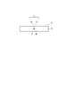
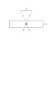
このような多光子吸収を利用する本実施形態に係るレーザ加工方法の原理について、図1〜図6を参照して説明する。図1に示すように、ウェハ状(板状)の加工対象物1の表面3には、加工対象物1を切断するための切断予定ライン5がある。切断予定ライン5は直線状に延びた仮想線である。本実施形態に係るレーザ加工方法では、図2に示すように、多光子吸収が生じる条件で加工対象物1の内部に集光点Pを合わせてレーザ光Lを照射して改質領域7を形成する。なお、集光点Pとは、レーザ光Lが集光する箇所のことである。また、切断予定ライン5は、直線状に限らず曲線状であってもよいし、仮想線に限らず加工対象物1に実際に引かれた線であってもよい。
The principle of the laser processing method according to this embodiment using such multiphoton absorption will be described with reference to FIGS. As shown in FIG. 1, there is a planned
そして、レーザ光Lを切断予定ライン5に沿って(すなわち、図1の矢印A方向に)相対的に移動させることにより、集光点Pを切断予定ライン5に沿って移動させる。これにより、図3〜図5に示すように、改質領域7が切断予定ライン5に沿って加工対象物1の内部に形成され、この改質領域7が切断起点領域8となる。ここで、切断起点領域8とは、加工対象物1が切断される際に切断(割れ)の起点となる領域を意味する。この切断起点領域8は、改質領域7が連続的に形成されることで形成される場合もあるし、改質領域7が断続的に形成されることで形成される場合もある。
Then, the condensing point P is moved along the planned
本実施形態に係るレーザ加工方法は、加工対象物1がレーザ光Lを吸収することにより加工対象物1を発熱させて改質領域7を形成するものではない。加工対象物1にレーザ光Lを透過させ加工対象物1の内部に多光子吸収を発生させて改質領域7を形成している。よって、加工対象物1の表面3ではレーザ光Lがほとんど吸収されないので、加工対象物1の表面3が溶融することはない。
The laser processing method according to the present embodiment does not form the modified
加工対象物1の内部に切断起点領域8を形成すると、この切断起点領域8を起点として割れが発生し易くなるため、図6に示すように、比較的小さな力で加工対象物1を切断することができる。よって、加工対象物1の表面3に不必要な割れを発生させることなく、加工対象物1を高精度に切断することが可能になる。
If the
この切断起点領域8を起点とした加工対象物1の切断には、次の2通りが考えられる。1つは、切断起点領域8形成後、加工対象物1に人為的な力が印加されることにより、切断起点領域8を起点として加工対象物1が割れ、加工対象物1が切断される場合である。これは、例えば加工対象物1の厚さが大きい場合の切断である。人為的な力が印加されるとは、例えば、加工対象物1の切断起点領域8に沿って加工対象物1に曲げ応力やせん断応力を加えたり、加工対象物1に温度差を与えることにより熱応力を発生させたりすることである。他の1つは、切断起点領域8を形成することにより、切断起点領域8を起点として加工対象物1の断面方向(厚さ方向)に向かって自然に割れ、結果的に加工対象物1が切断される場合である。これは、例えば加工対象物1の厚さが小さい場合には、1列の改質領域7により切断起点領域8が形成されることで可能となり、加工対象物1の厚さが大きい場合には、厚さ方向に複数列形成された改質領域7により切断起点領域8が形成されることで可能となる。なお、この自然に割れる場合も、切断する箇所において、切断起点領域8が形成されていない部位に対応する部分の表面3上にまで割れが先走ることがなく、切断起点領域8を形成した部位に対応する部分のみを割断することができるので、割断を制御よくすることができる。近年、シリコンウェハ等の加工対象物1の厚さは薄くなる傾向にあるので、このような制御性のよい割断方法は大変有効である。
The following two types of cutting of the
さて、本実施形態に係るレーザ加工方法において、多光子吸収により形成される改質領域としては、次の(1)〜(3)の場合がある。 In the laser processing method according to the present embodiment, there are the following cases (1) to (3) as modified regions formed by multiphoton absorption.
(1)改質領域が1つ又は複数のクラックを含むクラック領域の場合
加工対象物(例えばガラスやLiTaO3からなる圧電材料)の内部に集光点を合わせて、集光点における電界強度が1×10⁸(W/cm2)以上で且つパルス幅が1μs以下の条件でレーザ光を照射する。このパルス幅の大きさは、多光子吸収を生じさせつつ加工対象物の表面に余計なダメージを与えずに、加工対象物の内部にのみクラック領域を形成できる条件である。これにより、加工対象物の内部には多光子吸収による光学的損傷という現象が発生する。この光学的損傷により加工対象物の内部に熱ひずみが誘起され、これにより加工対象物の内部にクラック領域が形成される。電界強度の上限値としては、例えば1×1012(W/cm2)である。パルス幅は例えば1ns〜200nsが好ましい。なお、多光子吸収によるクラック領域の形成は、例えば、第45回レーザ熱加工研究会論文集(1998年.12月)の第23頁〜第28頁の「固体レーザー高調波によるガラス基板の内部マーキング」に記載されている。
(1) In the case where the modified region is a crack region including one or a plurality of cracks, the focusing point is set inside the object to be processed (for example, a piezoelectric material made of glass or LiTaO 3 ), and the electric field strength at the focusing point is Irradiation with laser light is performed under conditions of 1 × 10 8 (W / cm 2 ) or more and a pulse width of 1 μs or less. The magnitude of this pulse width is a condition that allows a crack region to be formed only inside the workpiece without causing extra damage to the surface of the workpiece while causing multiphoton absorption. As a result, a phenomenon of optical damage due to multiphoton absorption occurs inside the workpiece. This optical damage induces thermal strain inside the workpiece, thereby forming a crack region inside the workpiece. The upper limit value of the electric field strength is, for example, 1 × 10 12 (W / cm 2 ). The pulse width is preferably 1 ns to 200 ns, for example. The formation of the crack region by multiphoton absorption is described in, for example, “Inside of glass substrate by solid-state laser harmonics” on pages 23-28 of the 45th Laser Thermal Processing Research Papers (December 1998). It is described in “Marking”.
本発明者は、電界強度とクラックの大きさとの関係を実験により求めた。実験条件は次ぎの通りである。 The inventor obtained the relationship between the electric field strength and the size of the cracks by experiment. The experimental conditions are as follows.
(A)加工対象物:パイレックス(登録商標)ガラス(厚さ700μm)
(B)レーザ
光源:半導体レーザ励起Nd:YAGレーザ
波長:1064nm
レーザ光スポット断面積:3.14×10⁻⁸cm2
発振形態:Qスイッチパルス
繰り返し周波数:100kHz
パルス幅:30ns
出力:出力<1mJ/パルス
レーザ光品質:TEM00
偏光特性:直線偏光
(C)集光用レンズ
レーザ光波長に対する透過率:60パーセント
(D)加工対象物が載置される載置台の移動速度:100mm/秒
(A) Workpiece: Pyrex (registered trademark) glass (thickness 700 μm)
(B) Laser
Light source: Semiconductor laser pumped Nd: YAG laser
Wavelength: 1064nm
Laser light spot cross-sectional area: 3.14 × 10 −8 cm 2
Oscillation form: Q switch pulse
Repeat frequency: 100 kHz
Pulse width: 30ns
Output: Output <1mJ / pulse
Laser light quality: TEM 00
Polarization characteristics: Linearly polarized light (C) Condensing lens
Transmittance with respect to laser beam wavelength: 60% (D) Moving speed of mounting table on which workpiece is mounted: 100 mm / second
なお、レーザ光品質がTEM00とは、集光性が高くレーザ光の波長程度まで集光可能を意味する。 Note that the laser light quality TEM 00 means that the light condensing performance is high and the light can be condensed up to the wavelength of the laser light.
図7は上記実験の結果を示すグラフである。横軸はピークパワー密度であり、レーザ光がパルスレーザ光なので電界強度はピークパワー密度で表される。縦軸は1パルスのレーザ光により加工対象物の内部に形成されたクラック部分(クラックスポット)の大きさを示している。クラックスポットが集まりクラック領域となる。クラックスポットの大きさは、クラックスポットの形状のうち最大の長さとなる部分の大きさである。グラフ中の黒丸で示すデータは集光用レンズ(C)の倍率が100倍、開口数(NA)が0.80の場合である。一方、グラフ中の白丸で示すデータは集光用レンズ(C)の倍率が50倍、開口数(NA)が0.55の場合である。ピークパワー密度が1011(W/cm2)程度から加工対象物の内部にクラックスポットが発生し、ピークパワー密度が大きくなるに従いクラックスポットも大きくなることが分かる。 FIG. 7 is a graph showing the results of the experiment. The horizontal axis represents the peak power density. Since the laser beam is a pulsed laser beam, the electric field strength is represented by the peak power density. The vertical axis represents the size of a crack portion (crack spot) formed inside the workpiece by one pulse of laser light. Crack spots gather to form a crack region. The size of the crack spot is the size of the portion having the maximum length in the shape of the crack spot. Data indicated by black circles in the graph is for the case where the magnification of the condenser lens (C) is 100 times and the numerical aperture (NA) is 0.80. On the other hand, the data indicated by the white circles in the graph is when the magnification of the condenser lens (C) is 50 times and the numerical aperture (NA) is 0.55. From the peak power density of about 10 11 (W / cm 2 ), it can be seen that a crack spot is generated inside the workpiece, and the crack spot increases as the peak power density increases.
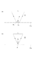
次に、クラック領域形成による加工対象物の切断のメカニズムについて、図8〜図11を参照して説明する。図8に示すように、多光子吸収が生じる条件で加工対象物1の内部に集光点Pを合わせてレーザ光Lを照射して切断予定ラインに沿って内部にクラック領域9を形成する。クラック領域9は1つ又は複数のクラックを含む領域である。このように形成されたクラック領域9が切断起点領域となる。図9に示すように、クラック領域9を起点として(すなわち、切断起点領域を起点として)クラックがさらに成長し、図10に示すように、クラックが加工対象物1の表面3と裏面21とに到達し、図11に示すように、加工対象物1が割れることにより加工対象物1が切断される。加工対象物1の表面3と裏面21とに到達するクラックは自然に成長する場合もあるし、加工対象物1に力が印加されることにより成長する場合もある。
Next, the mechanism of cutting the workpiece by forming the crack region will be described with reference to FIGS. As shown in FIG. 8, under the condition that multiphoton absorption occurs, the converging point P is aligned with the inside of the
(2)改質領域が溶融処理領域の場合
加工対象物(例えばシリコンのような半導体材料)の内部に集光点を合わせて、集光点における電界強度が1×10⁸(W/cm2)以上で且つパルス幅が1μs以下の条件でレーザ光を照射する。これにより加工対象物の内部は多光子吸収によって局所的に加熱される。この加熱により加工対象物の内部に溶融処理領域が形成される。溶融処理領域とは一旦溶融後再固化した領域や、まさに溶融状態の領域や、溶融状態から再固化する状態の領域であり、相変化した領域や結晶構造が変化した領域ということもできる。また、溶融処理領域とは単結晶構造、非晶質構造、多結晶構造において、ある構造が別の構造に変化した領域ということもできる。つまり、例えば、単結晶構造から非晶質構造に変化した領域、単結晶構造から多結晶構造に変化した領域、単結晶構造から非晶質構造及び多結晶構造を含む構造に変化した領域を意味する。加工対象物がシリコン単結晶構造の場合、溶融処理領域は例えば非晶質シリコン構造である。電界強度の上限値としては、例えば1×1012(W/cm2)である。パルス幅は例えば1ns〜200nsが好ましい。
(2) When the reforming region is a melt processing region The focusing point is set inside the object to be processed (for example, a semiconductor material such as silicon), and the electric field strength at the focusing point is 1 × 10 8 (W / cm 2). ) Irradiation with laser light is performed under the above conditions with a pulse width of 1 μs or less. As a result, the inside of the workpiece is locally heated by multiphoton absorption. By this heating, a melt processing region is formed inside the workpiece. The melt treatment region is a region once solidified after melting, a region in a molten state, or a region re-solidified from a molten state, and can also be referred to as a phase-changed region or a region in which the crystal structure has changed. The melt treatment region can also be said to be a region in which one structure is changed to another structure in a single crystal structure, an amorphous structure, or a polycrystalline structure. In other words, for example, a region changed from a single crystal structure to an amorphous structure, a region changed from a single crystal structure to a polycrystalline structure, or a region changed from a single crystal structure to a structure including an amorphous structure and a polycrystalline structure. To do. When the object to be processed has a silicon single crystal structure, the melt processing region has, for example, an amorphous silicon structure. The upper limit value of the electric field strength is, for example, 1 × 10 12 (W / cm 2 ). The pulse width is preferably 1 ns to 200 ns, for example.
本発明者は、シリコンウェハの内部で溶融処理領域が形成されることを実験により確認した。実験条件は次の通りである。 The inventor has confirmed through experiments that a melt-processed region is formed inside a silicon wafer. The experimental conditions are as follows.
(A)加工対象物:シリコンウェハ(厚さ350μm、外径4インチ)
(B)レーザ
光源:半導体レーザ励起Nd:YAGレーザ
波長:1064nm
レーザ光スポット断面積:3.14×10⁻⁸cm2
発振形態:Qスイッチパルス
繰り返し周波数:100kHz
パルス幅:30ns
出力:20μJ/パルス
レーザ光品質:TEM00
偏光特性:直線偏光
(C)集光用レンズ
倍率:50倍
N.A.:0.55
レーザ光波長に対する透過率:60パーセント
(D)加工対象物が載置される載置台の移動速度:100mm/秒
(A) Workpiece: silicon wafer (thickness 350 μm, outer diameter 4 inches)
(B) Laser
Light source: Semiconductor laser pumped Nd: YAG laser
Wavelength: 1064nm
Laser light spot cross-sectional area: 3.14 × 10 −8 cm 2
Oscillation form: Q switch pulse
Repeat frequency: 100 kHz
Pulse width: 30ns
Output: 20μJ / pulse
Laser light quality: TEM 00
Polarization characteristics: Linearly polarized light (C) Condensing lens
Magnification: 50 times
N. A. : 0.55
Transmittance with respect to laser beam wavelength: 60% (D) Moving speed of mounting table on which workpiece is mounted: 100 mm / second
図12は、上記条件でのレーザ加工により切断されたシリコンウェハの一部における断面の写真を表した図である。シリコンウェハ11の内部に溶融処理領域13が形成されている。なお、上記条件により形成された溶融処理領域13の厚さ方向の大きさは100μm程度である。
FIG. 12 is a view showing a photograph of a cross section of a part of a silicon wafer cut by laser processing under the above conditions. A
溶融処理領域13が多光子吸収により形成されたことを説明する。図13は、レーザ光の波長とシリコン基板の内部の透過率との関係を示すグラフである。ただし、シリコン基板の表面側と裏面側それぞれの反射成分を除去し、内部のみの透過率を示している。シリコン基板の厚さtが50μm、100μm、200μm、500μm、1000μmの各々について上記関係を示した。
The fact that the
例えば、Nd:YAGレーザの波長である1064nmにおいて、シリコン基板の厚さが500μm以下の場合、シリコン基板の内部ではレーザ光が80%以上透過することが分かる。図12に示すシリコンウェハ11の厚さは350μmであるので、多光子吸収による溶融処理領域13はシリコンウェハ11の中心付近、つまり表面から175μmの部分に形成される。この場合の透過率は、厚さ200μmのシリコンウェハを参考にすると、90%以上なので、レーザ光がシリコンウェハ11の内部で吸収されるのは僅かであり、ほとんどが透過する。このことは、シリコンウェハ11の内部でレーザ光が吸収されて、溶融処理領域13がシリコンウェハ11の内部に形成(つまりレーザ光による通常の加熱で溶融処理領域が形成)されたものではなく、溶融処理領域13が多光子吸収により形成されたことを意味する。多光子吸収による溶融処理領域の形成は、例えば、溶接学会全国大会講演概要第66集(2000年4月)の第72頁〜第73頁の「ピコ秒パルスレーザによるシリコンの加工特性評価」に記載されている。
For example, when the thickness of the silicon substrate is 500 μm or less at the wavelength of the Nd: YAG laser of 1064 nm, it can be seen that the laser light is transmitted by 80% or more inside the silicon substrate. Since the thickness of the
なお、シリコンウェハは、溶融処理領域によって形成される切断起点領域を起点として断面方向に向かって割れを発生させ、その割れがシリコンウェハの表面と裏面とに到達することにより、結果的に切断される。シリコンウェハの表面と裏面に到達するこの割れは自然に成長する場合もあるし、シリコンウェハに力が印加されることにより成長する場合もある。そして、切断起点領域からシリコンウェハの表面と裏面とに割れが自然に成長する場合には、切断起点領域を形成する溶融処理領域が溶融している状態から割れが成長する場合と、切断起点領域を形成する溶融処理領域が溶融している状態から再固化する際に割れが成長する場合とのいずれもある。ただし、どちらの場合も溶融処理領域はシリコンウェハの内部のみに形成され、切断後の切断面には、図12のように内部にのみ溶融処理領域が形成されている。このように、加工対象物の内部に溶融処理領域によって切断起点領域を形成すると、割断時、切断起点領域ラインから外れた不必要な割れが生じにくいので、割断制御が容易となる。ちなみに、溶融処理領域の形成は、多光子吸収が原因の場合のみでなく、他の吸収作用が原因の場合もある。 Note that a silicon wafer is cracked as a result of generating cracks in the cross-sectional direction starting from the cutting start region formed by the melt processing region and reaching the front and back surfaces of the silicon wafer. The The cracks that reach the front and back surfaces of the silicon wafer may grow naturally or may grow by applying force to the silicon wafer. And when a crack naturally grows from the cutting start region to the front and back surfaces of the silicon wafer, the case where the crack grows from a state where the melt treatment region forming the cutting starting region is melted, and the cutting starting region There are both cases where cracks grow when the solidified region is melted from the molten state. However, in either case, the melt processing region is formed only inside the silicon wafer, and the melt processing region is formed only inside the cut surface after cutting as shown in FIG. In this way, when the cutting start region is formed by the melt processing region inside the workpiece, unnecessary cracking off the cutting start region line is unlikely to occur during cleaving, so that cleaving control is facilitated. Incidentally, the formation of the melt processing region is not only caused by multiphoton absorption, but may also be caused by other absorption effects.
(3)改質領域が屈折率変化領域の場合
加工対象物(例えばガラス)の内部に集光点を合わせて、集光点における電界強度が1×10⁸(W/cm2)以上で且つパルス幅が1ns以下の条件でレーザ光を照射する。パルス幅を極めて短くして、多光子吸収を加工対象物の内部に起こさせると、多光子吸収によるエネルギーが熱エネルギーに転化せずに、加工対象物の内部にはイオン価数変化、結晶化又は分極配向等の永続的な構造変化が誘起されて屈折率変化領域が形成される。電界強度の上限値としては、例えば1×1012(W/cm2)である。パルス幅は例えば1ns以下が好ましく、1ps以下がさらに好ましい。多光子吸収による屈折率変化領域の形成は、例えば、第42回レーザ熱加工研究会論文集(1997年.11月)の第105頁〜第111頁の「フェムト秒レーザー照射によるガラス内部への光誘起構造形成」に記載されている。
(3) When the modified region is a refractive index changing region The focusing point is set inside the object to be processed (for example, glass), and the electric field intensity at the focusing point is 1 × 10 8 (W / cm 2 ) or more. Laser light is irradiated under the condition that the pulse width is 1 ns or less. When the pulse width is made extremely short and multiphoton absorption occurs inside the workpiece, the energy due to the multiphoton absorption is not converted into thermal energy, and the ion valence change and crystallization occur inside the workpiece. Alternatively, a permanent structural change such as polarization orientation is induced to form a refractive index change region. The upper limit value of the electric field strength is, for example, 1 × 10 12 (W / cm 2 ). For example, the pulse width is preferably 1 ns or less, and more preferably 1 ps or less. The formation of the refractive index changing region by multiphoton absorption is described in, for example, “The Femtosecond Laser Irradiation to the Inside of Glass” on
以上、多光子吸収により形成される改質領域として(1)〜(3)の場合を説明したが、ウェハ状の加工対象物の結晶構造やその劈開性などを考慮して切断起点領域を次のように形成すれば、その切断起点領域を起点として、より一層小さな力で、しかも精度良く加工対象物を切断することが可能になる。 As described above, the cases of (1) to (3) have been described as the modified regions formed by multiphoton absorption. However, considering the crystal structure of the wafer-like workpiece and its cleavage property, the cutting origin region is described below. If it forms in this way, it will become possible to cut | disconnect a process target object with much smaller force from the cutting | disconnection starting point area | region as a starting point with still smaller force.
すなわち、シリコンなどのダイヤモンド構造の単結晶半導体からなる基板の場合は、(111)面(第1劈開面)や(110)面(第2劈開面)に沿った方向に切断起点領域を形成するのが好ましい。また、GaAsなどの閃亜鉛鉱型構造のIII−V族化合物半導体からなる基板の場合は、(110)面に沿った方向に切断起点領域を形成するのが好ましい。さらに、サファイア(Al2O3)などの六方晶系の結晶構造を有する基板の場合は、(0001)面(C面)を主面として(1120)面(A面)或いは(1100)面(M面)に沿った方向に切断起点領域を形成するのが好ましい。 That is, in the case of a substrate made of a single crystal semiconductor having a diamond structure such as silicon, the cutting start region is formed in a direction along the (111) plane (first cleavage plane) or the (110) plane (second cleavage plane). Is preferred. In the case of a substrate made of a zinc-blende-type III-V group compound semiconductor such as GaAs, it is preferable to form the cutting start region in the direction along the (110) plane. Further, in the case of a substrate having a hexagonal crystal structure such as sapphire (Al 2 O 3 ), the (1120) plane (A plane) or (1100) plane ( It is preferable to form the cutting start region in a direction along the (M plane).
なお、上述した切断起点領域を形成すべき方向(例えば、単結晶シリコン基板における(111)面に沿った方向)、或いは切断起点領域を形成すべき方向に直交する方向に沿って基板にオリエンテーションフラットを形成すれば、そのオリエンテーションフラットを基準とすることで、切断起点領域を形成すべき方向に沿った切断起点領域を容易且つ正確に基板に形成することが可能になる。 Note that the orientation flat on the substrate along the direction in which the above-described cutting start region is to be formed (for example, the direction along the (111) plane in the single crystal silicon substrate) or the direction perpendicular to the direction in which the cutting start region is to be formed. By using the orientation flat as a reference, it is possible to easily and accurately form the cutting start area along the direction in which the cutting start area is to be formed on the substrate.
次に、本発明の好適な実施形態について説明する。 Next, a preferred embodiment of the present invention will be described.
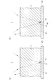
図14及び図15に示すように、加工対象物1は、いわゆるMEMSウェハであり、厚さ300μmのシリコンウェハ(半導体基板)11と、複数の機能素子15を含んでシリコンウェハ11の表面に形成された機能素子層16と、シリコンウェハ11の裏面に形成された金属膜17と、を備えている。機能素子15は、例えば、機械要素部品、センサ、アクチュエータ、電子回路等であり、シリコンウェハ11のオリエンテーションフラット6に平行な方向及び垂直な方向にマトリックス状に多数形成されている。金属膜17は金からなり、その厚さは3μmである。
As shown in FIGS. 14 and 15, the
以上のように構成された加工対象物1を以下のようにして機能素子15毎に切断する。まず、図16に示すように、加工対象物1の裏面21、すなわち金属膜17の裏面にエキスパンドテープ23を貼り付ける。そして、機能素子層16を上側にして加工対象物1をレーザ加工装置の載置台(図示せず)上に固定する。
The
続いて、図17に示すように、加工対象物1の表面3、すなわち機能素子層16の表面をレーザ光入射面として、シリコンウェハ11の表面から320μmの位置(シリコンウェハ11の外部)が集光点となる集光用レンズの位置(加工対象物のレーザ光入射面(ここでは、表面3)に対向するレーザ光反射面(ここでは、金属膜17の表面17a)をレーザ光が透過すると仮定した場合。以下、同様。)でレーザ光Lを照射し、載置台の移動によって、隣り合う機能素子15,15間を通るように格子状に設定された切断予定ライン5(図14の破線参照)に沿ってレーザ光Lをスキャンする。
Subsequently, as shown in FIG. 17, the
このとき、加工対象物1の表面3に対向する金属膜17の表面(所定の面)17a、すなわち金属膜17におけるレーザ光入射面側の面でレーザ光Lが反射され、その反射光RLがシリコンウェハ11に照射されて、シリコンウェハ11の内部における裏面21の極近傍に集光する。これにより、シリコンウェハ11の内部における裏面21の極近傍に、溶融処理領域131及び微小空洞14が切断予定ライン5に沿って形成される。なお、この場合のレーザ光の照射条件は、パルス幅150ns、エネルギー15μJである。また、上述した「シリコンウェハ11の表面から320μmの位置」は、球面収差等を考慮しない理論上の「集光点Pを合わせる位置」を意味している。
At this time, the laser light L is reflected by the surface (predetermined surface) 17a of the
ここで、微小空洞14について説明する。一般的に、シリコンウェハ11の内部に集光点を合わせて、集光点におけるピークパワー密度が1×10⁸(W/cm2)以上で且つパルス幅が1μs以下の条件でレーザ光を照射すると、シリコンウェハ11の内部に、溶融処理領域13及び微小空洞14が対になって形成される場合がある。微小空洞14は、溶融処理領域13と離れて形成される場合もあるし、溶融処理領域13と連続して形成される場合もあるが、レーザ光の進行方向において溶融処理領域13の下流側に形成される。上述した場合では、微小空洞14が溶融処理領域131に対して加工対象物1の表面3側に形成されているため、溶融処理領域131及び微小空洞14の形成に反射光RLが寄与しているといえる。なお、溶融処理領域13及び微小空洞14が対になって形成される原理については、特開2005−57257号公報に詳細に記載されている。
Here, the
更に、図18に示すように、加工対象物1の表面3をレーザ光入射面としてシリコンウェハ11の内部に集光点Pを合わせてレーザ光Lを照射し、載置台の移動によって、隣り合う機能素子15,15間を通るように格子状に設定された切断予定ライン5に沿ってレーザ光Lをスキャンする。
Further, as shown in FIG. 18, the
この切断予定ライン5に沿ったレーザ光Lのスキャンを1本の切断予定ライン5に対して5回行うが、シリコンウェハ11の表面と集光点Pを合わせる位置との距離を各回毎に変えることで、溶融処理領域131とシリコンウェハ11の表面との間に、5列の溶融処理領域132を切断予定ライン5に沿って形成する。なお、1本の切断予定ライン5に対してシリコンウェハ11の内部に形成される溶融処理領域132の列数は、シリコンウェハ11の厚さ等に応じて変化するものであり、5列に限定されない。また、各溶融処理領域132に対して加工対象物1の裏面21側に、溶融処理領域132と対になる微小空洞14が形成される場合がある。また、溶融処理領域131,132には、クラックが混在する場合もある。
The scanning of the laser beam L along the
続いて、図19に示すように、エキスパンドテープ23を拡張させ、溶融処理領域131,132を切断の起点として、切断予定ライン5に沿って加工対象物1を切断する。このとき、エキスパンドテープ23が拡張させられているため、切断されることで得られた複数の半導体チップ25が互いに離間することになる。
Subsequently, as shown in FIG. 19, the
なお、上述したレーザ加工方法は、図26に示すレーザ加工装置によって実施される。図26に示すように、レーザ加工装置100は、レーザ光Lを出射するレーザ光源101と、レーザ光Lの光軸の向きを90°変えるように配置されたダイクロイックミラー103と、レーザ光Lを集光するための集光用レンズ105と、を備えている。また、レーザ加工装置100は、集光用レンズ105で集光されたレーザ光Lが照射される加工対象物1を支持するための載置台107と、載置台107をX、Y、Z軸方向に移動させるためのステージ111と、レーザ光Lの出力やパルス幅等の調節やステージ111の移動等、レーザ加工装置100の全体を制御する制御部115と、を備えている。
The above-described laser processing method is performed by the laser processing apparatus shown in FIG. As shown in FIG. 26, the
このレーザ加工装置100においては、レーザ光源101から出射されたレーザ光Lは、ダイクロイックミラー103によってその光軸の向きを90°変えられ、載置台107上に載置された加工対象物1に向かって集光用レンズ105によって集光される。これと共に、ステージ111が移動させられ、加工対象物1がレーザ光Lに対して切断予定ライン5に沿って相対移動させられる。これにより、切断予定ライン5に沿って、切断の起点となる改質領域が加工対象物1に形成されることとなる。
In this
以上説明したように、上述したレーザ加工方法では、加工対象物1のレーザ光入射面である表面3に対向する金属膜17の表面17aで反射されたレーザ光Lの反射光RLをシリコンウェハ11に照射することで、6列の溶融処理領域131,132のうち、金属膜17の表面17aに最も近い溶融処理領域131を形成している。これにより、図20に示すように、溶融処理領域131を金属膜17の表面17aの極近傍に形成することができる。シリコンウェハ11の厚さが切断予定ライン5に沿って変化している場合や、シリコンウェハ11が高濃度ドープウェハ等で、レーザ光Lの透過率が低い場合等で表面17aの近傍で且つ同じ高さ位置を保って溶融処理領域131を切断予定ライン5に沿って形成することが困難であっても、このように、金属膜17の表面17aに最も近い溶融処理領域131の形成に反射光RLを利用することで、切断予定ライン5に沿って溶融処理領域131を金属膜17の表面17aの極近傍に高い密度で安定して形成することができる。そのため、加工対象物1を切断した際に切断面の裏面21側の端部が切断予定ライン5から外れるのを防止して、加工対象物1を切断予定ライン5に沿って精度良く切断することが可能となる。
As described above, in the laser processing method described above, the reflected light RL of the laser light L reflected from the
ここで、金属膜17の表面17aで反射されたレーザ光Lの反射光RLを利用した場合に、溶融処理領域131が金属膜17の表面17aの極近傍に形成される原理について説明する。
Here, in the case of using reflected light RL of the laser light L reflected by the
本発明者が推測する第1の原理は、次の通りである。図21に示すように、シリコンウェハ11の裏面、すなわち金属膜17の表面17a近傍に集光点を合わせてレーザ光Lを照射すると、球面収差の影響で、中心光線と周囲光線との集光度が劣化し、各光線が一点に集光せず、各光線、特に周囲光線の集光箇所がレーザ光Lの光軸方向にずれる。これにより、金属膜17の表面17a下で集光するように進行する光線の集光箇所が、金属膜17の表面17aでの反射によって、金属膜17の表面17a上で集光する光線の集光箇所に補完される。従って、切断予定ライン5に沿って溶融処理領域131が金属膜17の表面17aの極近傍に高い密度で形成されることになる。球面収差を考えなければ理論的には、溶融処理領域131は集光点の位置であるシリコンウェハ11の裏面上に形成されるはずであるが、反射による影響で溶融処理領域131の形成位置が上側にずれるともいえる。
The first principle estimated by the present inventor is as follows. As shown in FIG. 21, when the laser beam L is irradiated with the condensing point on the back surface of the
本発明者が推測する第2の原理は、次の通りである。図22(a)に示すように、シリコンウェハ11の外部が集光点となる集光用レンズの位置、すなわち金属膜17の表面17a下に集光点を合わせてレーザ光Lを照射すると、金属膜17の表面17aでレーザ光Lが反射されて、その反射光RLがシリコンウェハ11の内部に集光する。金属膜17の表面17aで反射される前には集光度が低いためレーザ光Lがシリコンウェハ11に殆ど吸収されず、反射光RLの集光点Pの位置で局所的に高温となる。そのため、吸収係数の温度依存性により集光点Pの位置で吸収係数が高まり反射光RLの集光点Pの位置から、反射光RLの進行方向において集光点Pの上流側(反射表面17a側)で反射光RLが吸収され易くなる。その結果、切断予定ライン5に沿って溶融処理領域131が金属膜17の表面17aの極近傍に高い密度で(すなわち、分割性の高い改質領域として)形成されることになる。
The second principle estimated by the present inventor is as follows. As shown in FIG. 22A, when the laser beam L is irradiated with the focusing point positioned below the
なお、図22(b)に示すように、シリコンウェハ11の内部、すなわち金属膜17の表面17a上に集光点Pを合わせてレーザ光Lを照射すると、集光点Pの上側の位置でも温度が高くなる。そのため、吸収係数の温度依存性により集光点Pの上側の位置で吸収係数が高まり、レーザ光Lの吸収が始まる。これにより、レーザ光Lの進行方向において集光点Pの近傍に進行するレーザ光Lが減少し、集光点Pの上側の部分がレーザ光Lの光軸に沿って局所的に高温となる。そのため、吸収係数の温度依存性により集光点Pの上側の部分で吸収係数が高まり、レーザ光Lが吸収される。その結果、溶融処理領域13の形成に利用し得るレーザ光Lのエネルギーが減少するため、切断予定ライン5に沿って溶融処理領域13が金属膜17の表面17a(の近傍)から若干離れた上側の位置に低い密度で形成されることになる。これは、厚いウェハにおいてはレーザ光入射面から深い位置になるほど吸収の影響が大きくなってレーザ光のエネルギーが減少し、加工閾値を超えるためには吸収による温度依存の影響が無視できないからであると推測される。
As shown in FIG. 22B, when the laser beam L is irradiated with the condensing point P on the inside of the
本発明は、上記実施形態に限定されるものではない。 The present invention is not limited to the above embodiment.
例えば、上記実施形態では、金属膜17の表面17aで反射されたレーザ光Lの反射光RLをシリコンウェハ11に照射することで、金属膜17の表面17aの極近傍に溶融処理領域131を形成したが、図23及び図24に示すように、加工対象物1の表面3の極近傍に溶融処理領域131を形成してもよい。この場合には、加工対象物1の表面3をレーザ光入射面として、シリコンウェハ11の表面から600μmの位置(シリコンウェハ11の外部)に集光点を合わせて、パルス幅150ns、エネルギー15μJの条件でレーザ光Lを照射する。これにより、上述した吸収係数の温度依存性に起因して加工対象物1の表面3が溶融等の損傷を受けるのを防止して、加工対象物1の表面3の極近傍に溶融処理領域131を形成することができる。しかも、加工対象物1を切断した際に切断面の表面3側の端部が切断予定ライン5から外れるのを防止して、加工対象物1を切断予定ライン5に沿って精度良く切断することが可能となる。
For example, in the above embodiment, by irradiating the reflected light RL of the laser light L reflected by the
なお、金属膜17の表面17aに最も近い溶融処理領域13や、加工対象物1の表面3に最も近い溶融処理領域13だけでなく、複数列の溶融処理領域13のうち、金属膜17の表面17aに最も近い溶融処理領域13、及び加工対象物1の表面3に最も近い溶融処理領域13の少なくとも1列を含む複数列の溶融処理領域13を、金属膜17の表面17aで反射されたレーザ光Lの反射光RLを利用して形成してもよい。
It should be noted that the surface of the
また、図25に示すように、金属膜17の表面17aに最も近い溶融処理領域131を形成すると同時に、加工対象物1の裏面21に、所定の深さを有する弱化領域18を切断予定ライン5に沿って形成してもよい。この場合には、加工対象物1の表面3をレーザ光入射面として、シリコンウェハ11の表面から305μmの位置(シリコンウェハ11の外部)に集光点を合わせて、パルス幅150ns、エネルギー15μJの条件でレーザ光Lを照射する。このとき、加工対象物1の裏面21は金属膜17の裏面であるが、この場合であっても、所定の深さを有する弱化領域18が切断予定ライン5に沿って金属膜17に形成されているため、比較的小さな外力で、切断予定ライン5に沿って加工対象物1を精度良く切断することが可能となる。しかも、溶融処理領域131がシリコンウェハ11の内部に形成されているため、溶融処理領域131からパーティクルが発生するのを防止することができる。
Further, as shown in FIG. 25, at the same time forms the closest molten processed
また、上記実施形態では、レーザ光Lを反射する面が金属膜17の表面17aであったが、加工対象物1が金属膜17を備えず、例えば、レーザ光Lを反射する面がシリコンウェハ11の裏面であってもよい。この場合には、レーザ光Lがシリコンウェハ11の裏面で一部反射されて、その反射光RLがシリコンウェハ11に照射されることになる。そして、機能素子15は、例えば、結晶成長により形成された半導体動作層、フォトダイオード等の受光素子、レーザダイオード等の発光素子、或いは回路として形成された回路素子等であってもよい。
Moreover, in the said embodiment, although the surface which reflects the laser beam L was the
また、上記実施形態では、加工対象物1の表面3をレーザ光入射面としたが、加工対象物1が金属膜17を備えない場合には、加工対象物1の裏面21をレーザ光入射面としてもよい。加工対象物1の裏面21をレーザ光入射面とする場合には、一例として、次のように加工対象物1を複数の半導体チップ25に切断する。すなわち、機能素子層16の表面に保護テープを貼り付け、保護テープにより機能素子層16を保護した状態で、レーザ加工装置の載置台に、加工対象物1を保持した保護テープを固定する。そして、加工対象物1の裏面21をレーザ光入射面としてシリコンウェハ11にレーザ光Lを照射することにより、切断予定ライン5に沿って溶融処理領域131,132を形成する。続いて、載置台に固定された保護テープを加工対象物1と共に離隔させる。そして、加工対象物1の裏面21にエキスパンドテープ23を貼り付けて、機能素子層16の表面から保護テープを剥がした後、エキスパンドテープ23を拡張させて、溶融処理領域131,132を切断の起点として加工対象物1を切断予定ライン5に沿って切断すると共に、切断されることで得られた複数の半導体チップ25を互いに離間させる。
Moreover, in the said embodiment, although the
また、上記実施形態では、シリコンウェハ11の内部に溶融処理領域131,132を形成したが、ガラスや圧電材料等、他の材料からなるウェハの内部に、クラック領域や屈折率変化領域等、他の改質領域を形成してもよい。
In the above embodiment, inside molten processed
また、次のようにして改質領域7を加工対象物1に形成してもよい。まず、図27(a)に示すように、加工対象物1のレーザ光入射面(ここでは、表面3)に対向するレーザ光反射面(ここでは、裏面21)の近傍の位置が集光点Pとなるようにレーザ光Lを照射することで改質領域7aを形成する。その後、図27(b)に示すように、レーザ光反射面をレーザ光が透過すると仮定した場合にレーザ光Lの進行方向においてレーザ光反射面の下流側(レーザ光反射面に対してレーザ光源(レーザ光出射側)と反対側)の位置が集光点Pとなるようにレーザ光Lを照射することでその反射光RLにより改質領域7bを形成する。このように、改質領域7aと改質領域7bとを重ねて形成することで、密度が高い(すなわち、分割性が高い)改質領域7を加工対象物1に形成することができる。
Further, the modified
加工対象物1にレーザ光Lを照射することにより、1本の切断予定ライン5に沿って加工対象物1の厚さ方向に並ぶように複数列の改質領域7を加工対象物1の少なくとも内部に形成する場合に限定されず、1本の切断予定ライン5に沿って1列の改質領域7を加工対象物1の少なくとも内部に形成してもよい。
By irradiating the
1…加工対象物、3…表面(レーザ光入射面)、5…切断予定ライン、11…シリコンウェハ(半導体基板)、131,132…溶融処理領域(改質領域)、17…金属膜、17a…表面(所定の面)、L…レーザ光、RL…反射光。
1 ... workpiece, 3 ... surface (laser light entrance surface), 5 ... line to cut, 11 ... silicon wafer (semiconductor substrate), 13 1, 13 2 ... molten processed region (modified region), 17 ...
Claims (9)
前記加工対象物においてレーザ光が入射するレーザ光入射面に対向し且つ前記加工対象物が備える金属膜における前記レーザ光入射面側の面である所定の面で反射されたレーザ光の反射光を前記加工対象物に照射することにより、複数列の前記改質領域のうち、前記所定の面に最も近い改質領域及び前記レーザ光入射面に最も近い改質領域の少なくとも1列を含む1列又は複数列の改質領域を形成し、
前記所定の面に最も近い前記改質領域を形成する場合には、当該改質領域を形成すると同時に、前記切断予定ラインに沿って弱化領域を前記金属膜に形成することを特徴とするレーザ加工方法。 By irradiating a plate-like workpiece with laser light, modification of a plurality of rows serving as starting points of cutting so as to line up in the thickness direction of the workpiece along the planned cutting line of the workpiece A laser processing method for forming a region inside the workpiece,
The workpiece the laser light to face the incident surface and the workpiece reflected light of the reflected laser beams in the plane der Ru predetermined surface of the laser light incident surface side of the metal film included in the laser light is incident at 1 to include at least one row of a modified region closest to the predetermined surface and a modified region closest to the laser light incident surface among a plurality of the modified regions. Forming a modified region of a row or multiple rows ,
When forming the modified region closest to the predetermined surface, the weakened region is formed in the metal film along the planned cutting line at the same time as forming the modified region. Method.
前記加工対象物のレーザ光入射面に対向し且つ前記加工対象物が備える金属膜における前記レーザ光入射面側の面であるレーザ光反射面をレーザ光が透過すると仮定した場合に、レーザ光の進行方向において前記レーザ光反射面の下流側の位置が、レーザ光を前記加工対象物に集光するための集光用レンズによって集光されるレーザ光の集光点となるように、前記集光用レンズを配置し、前記加工対象物にレーザ光を照射することにより、複数列の前記改質領域のうち、前記レーザ光反射面に最も近い改質領域及び前記レーザ光入射面に最も近い改質領域の少なくとも1列を含む1列又は複数列の改質領域を形成し、
前記レーザ光反射面に最も近い前記改質領域を形成する場合には、当該改質領域を形成すると同時に、前記切断予定ラインに沿って弱化領域を前記金属膜に形成することを特徴とするレーザ加工方法。 By irradiating a plate-like workpiece with laser light , modification of a plurality of rows serving as starting points of cutting so as to line up in the thickness direction of the workpiece along the planned cutting line of the workpiece A laser processing method for forming a region inside the workpiece,
When said laser beam opposite to the incident surface and the surface der of the the metal film workpiece comprises laser light entrance surface side Ru laser light reflecting surface of the laser beam of the object is assumed to transmit a laser beam The downstream position of the laser light reflecting surface in the traveling direction is a condensing point of the laser light collected by a condensing lens for condensing the laser light on the workpiece. By arranging a condensing lens and irradiating the workpiece with laser light , among the modified regions in a plurality of rows, the modified region closest to the laser light reflecting surface and the laser light incident surface Forming one or more modified regions including at least one row of near modified regions ;
When forming the modified region closest to the laser light reflecting surface, a weakened region is formed in the metal film along the planned cutting line simultaneously with forming the modified region. Processing method.
前記加工対象物のレーザ光入射面に対向し且つ前記加工対象物が備える金属膜における前記レーザ光入射面側の面であるレーザ光反射面をレーザ光が透過すると仮定した場合に、レーザ光の進行方向において前記レーザ光反射面の下流側の位置が、レーザ光を前記加工対象物に集光するための集光用レンズによって集光されるレーザ光の集光点となるように、前記集光用レンズを配置し、前記加工対象物にレーザ光を照射することにより、複数列の前記改質領域のうち、前記レーザ光反射面に最も近い改質領域及び前記レーザ光入射面に最も近い改質領域の少なくとも1列を含む1列又は複数列の改質領域を形成し、
前記レーザ光反射面に最も近い前記改質領域を形成する場合には、当該改質領域を形成すると同時に、前記切断予定ラインに沿って弱化領域を前記金属膜に形成することを特徴とするレーザ加工装置。 By irradiating a plate-like workpiece with laser light , modification of a plurality of rows serving as starting points of cutting so as to line up in the thickness direction of the workpiece along the planned cutting line of the workpiece A laser processing apparatus for forming a region inside the workpiece,
When said laser beam opposite to the incident surface and the surface der of the the metal film workpiece comprises laser light entrance surface side Ru laser light reflecting surface of the laser beam of the object is assumed to transmit a laser beam The downstream position of the laser light reflecting surface in the traveling direction is a condensing point of the laser light collected by a condensing lens for condensing the laser light on the workpiece. By arranging a condensing lens and irradiating the workpiece with laser light , among the modified regions in a plurality of rows, the modified region closest to the laser light reflecting surface and the laser light incident surface Forming one or more modified regions including at least one row of near modified regions ;
When forming the modified region closest to the laser light reflecting surface, a weakened region is formed in the metal film along the planned cutting line simultaneously with forming the modified region. Processing equipment.
Priority Applications (1)
| Application Number | Priority Date | Filing Date | Title |
|---|---|---|---|
| JP2007242846A JP5322418B2 (en) | 2006-09-19 | 2007-09-19 | Laser processing method and laser processing apparatus |
Applications Claiming Priority (3)
| Application Number | Priority Date | Filing Date | Title |
|---|---|---|---|
| JP2006253259 | 2006-09-19 | ||
| JP2006253259 | 2006-09-19 | ||
| JP2007242846A JP5322418B2 (en) | 2006-09-19 | 2007-09-19 | Laser processing method and laser processing apparatus |
Publications (3)
| Publication Number | Publication Date |
|---|---|
| JP2008100284A JP2008100284A (en) | 2008-05-01 |
| JP2008100284A5 JP2008100284A5 (en) | 2009-07-23 |
| JP5322418B2 true JP5322418B2 (en) | 2013-10-23 |
Family
ID=39434998
Family Applications (1)
| Application Number | Title | Priority Date | Filing Date |
|---|---|---|---|
| JP2007242846A Active JP5322418B2 (en) | 2006-09-19 | 2007-09-19 | Laser processing method and laser processing apparatus |
Country Status (1)
| Country | Link |
|---|---|
| JP (1) | JP5322418B2 (en) |
Cited By (4)
| Publication number | Priority date | Publication date | Assignee | Title |
|---|---|---|---|---|
| US10562130B1 (en) | 2018-12-29 | 2020-02-18 | Cree, Inc. | Laser-assisted method for parting crystalline material |
| US10576585B1 (en) | 2018-12-29 | 2020-03-03 | Cree, Inc. | Laser-assisted method for parting crystalline material |
| US10611052B1 (en) | 2019-05-17 | 2020-04-07 | Cree, Inc. | Silicon carbide wafers with relaxed positive bow and related methods |
| US11024501B2 (en) | 2018-12-29 | 2021-06-01 | Cree, Inc. | Carrier-assisted method for parting crystalline material along laser damage region |
Families Citing this family (7)
| Publication number | Priority date | Publication date | Assignee | Title |
|---|---|---|---|---|
| JP5491761B2 (en) * | 2009-04-20 | 2014-05-14 | 浜松ホトニクス株式会社 | Laser processing equipment |
| CN103079747B (en) * | 2010-07-12 | 2016-08-03 | 罗芬-西纳技术有限公司 | The method being carried out material process by laser filament effect |
| JP5658043B2 (en) * | 2011-01-07 | 2015-01-21 | 株式会社ディスコ | Split method |
| JP2012238746A (en) | 2011-05-12 | 2012-12-06 | Disco Abrasive Syst Ltd | Division method of optical device wafer |
| JP2014082317A (en) * | 2012-10-16 | 2014-05-08 | Disco Abrasive Syst Ltd | Wafer processing method |
| JP6189066B2 (en) * | 2013-03-27 | 2017-08-30 | 株式会社ディスコ | Wafer processing method |
| CN112518141B (en) * | 2020-11-24 | 2022-07-15 | 无锡光导精密科技有限公司 | Laser induced cutting method and device |
Family Cites Families (2)
| Publication number | Priority date | Publication date | Assignee | Title |
|---|---|---|---|---|
| JP3626442B2 (en) * | 2000-09-13 | 2005-03-09 | 浜松ホトニクス株式会社 | Laser processing method |
| JP4424302B2 (en) * | 2005-11-16 | 2010-03-03 | 株式会社デンソー | Manufacturing method of semiconductor chip |
-
2007
- 2007-09-19 JP JP2007242846A patent/JP5322418B2/en active Active
Cited By (10)
| Publication number | Priority date | Publication date | Assignee | Title |
|---|---|---|---|---|
| US10562130B1 (en) | 2018-12-29 | 2020-02-18 | Cree, Inc. | Laser-assisted method for parting crystalline material |
| US10576585B1 (en) | 2018-12-29 | 2020-03-03 | Cree, Inc. | Laser-assisted method for parting crystalline material |
| US11024501B2 (en) | 2018-12-29 | 2021-06-01 | Cree, Inc. | Carrier-assisted method for parting crystalline material along laser damage region |
| US11219966B1 (en) | 2018-12-29 | 2022-01-11 | Wolfspeed, Inc. | Laser-assisted method for parting crystalline material |
| US11826846B2 (en) | 2018-12-29 | 2023-11-28 | Wolfspeed, Inc. | Laser-assisted method for parting crystalline material |
| US11901181B2 (en) | 2018-12-29 | 2024-02-13 | Wolfspeed, Inc. | Carrier-assisted method for parting crystalline material along laser damage region |
| US11911842B2 (en) | 2018-12-29 | 2024-02-27 | Wolfspeed, Inc. | Laser-assisted method for parting crystalline material |
| US10611052B1 (en) | 2019-05-17 | 2020-04-07 | Cree, Inc. | Silicon carbide wafers with relaxed positive bow and related methods |
| US11034056B2 (en) | 2019-05-17 | 2021-06-15 | Cree, Inc. | Silicon carbide wafers with relaxed positive bow and related methods |
| US11654596B2 (en) | 2019-05-17 | 2023-05-23 | Wolfspeed, Inc. | Silicon carbide wafers with relaxed positive bow and related methods |
Also Published As
| Publication number | Publication date |
|---|---|
| JP2008100284A (en) | 2008-05-01 |
Similar Documents
| Publication | Publication Date | Title |
|---|---|---|
| JP4954653B2 (en) | Laser processing method | |
| JP5322418B2 (en) | Laser processing method and laser processing apparatus | |
| JP4197693B2 (en) | Laser processing method and semiconductor device | |
| JP4198123B2 (en) | Laser processing method | |
| JP4907984B2 (en) | Laser processing method and semiconductor chip | |
| JP4907965B2 (en) | Laser processing method | |
| KR101428823B1 (en) | Laser processing method and laser processing apparatus | |
| JP5138219B2 (en) | Laser processing method | |
| JP4917257B2 (en) | Laser processing method | |
| JP4536407B2 (en) | Laser processing method and object to be processed | |
| JP4776994B2 (en) | Processing object cutting method | |
| JP4781661B2 (en) | Laser processing method | |
| JP4829781B2 (en) | Laser processing method and semiconductor chip | |
| JP5312761B2 (en) | Cutting method | |
| JP2007142206A (en) | Laser machining method | |
| JP2009206534A (en) | Method of forming cutting start area | |
| JP5177992B2 (en) | Processing object cutting method | |
| JP2005012203A (en) | Laser machining method | |
| JP5122161B2 (en) | Processing object cutting method | |
| JP2008110400A (en) | Laser processing method |
Legal Events
| Date | Code | Title | Description |
|---|---|---|---|
| A521 | Written amendment |
Free format text: JAPANESE INTERMEDIATE CODE: A523 Effective date: 20090608 |
|
| A621 | Written request for application examination |
Free format text: JAPANESE INTERMEDIATE CODE: A621 Effective date: 20100902 |
|
| A977 | Report on retrieval |
Free format text: JAPANESE INTERMEDIATE CODE: A971007 Effective date: 20120206 |
|
| A131 | Notification of reasons for refusal |
Free format text: JAPANESE INTERMEDIATE CODE: A131 Effective date: 20120619 |
|
| A521 | Written amendment |
Free format text: JAPANESE INTERMEDIATE CODE: A523 Effective date: 20120820 |
|
| A131 | Notification of reasons for refusal |
Free format text: JAPANESE INTERMEDIATE CODE: A131 Effective date: 20130108 |
|
| TRDD | Decision of grant or rejection written | ||
| A01 | Written decision to grant a patent or to grant a registration (utility model) |
Free format text: JAPANESE INTERMEDIATE CODE: A01 Effective date: 20130618 |
|
| A61 | First payment of annual fees (during grant procedure) |
Free format text: JAPANESE INTERMEDIATE CODE: A61 Effective date: 20130716 |
|
| R150 | Certificate of patent or registration of utility model |
Ref document number: 5322418 Country of ref document: JP Free format text: JAPANESE INTERMEDIATE CODE: R150 Free format text: JAPANESE INTERMEDIATE CODE: R150 |