JP2005012203A - Laser machining method - Google Patents
Laser machining method Download PDFInfo
- Publication number
- JP2005012203A JP2005012203A JP2004157965A JP2004157965A JP2005012203A JP 2005012203 A JP2005012203 A JP 2005012203A JP 2004157965 A JP2004157965 A JP 2004157965A JP 2004157965 A JP2004157965 A JP 2004157965A JP 2005012203 A JP2005012203 A JP 2005012203A
- Authority
- JP
- Japan
- Prior art keywords
- region
- workpiece
- cutting
- laser
- forming
- Prior art date
- Legal status (The legal status is an assumption and is not a legal conclusion. Google has not performed a legal analysis and makes no representation as to the accuracy of the status listed.)
- Pending
Links
Images


Landscapes
- Processing Of Stones Or Stones Resemblance Materials (AREA)
- Laser Beam Processing (AREA)
- Dicing (AREA)
Abstract
Description
本発明は、半導体材料基板、圧電材料基板やガラス基板等の加工対象物の切断に使用されるレーザ加工方法に関する。 The present invention relates to a laser processing method used for cutting an object to be processed such as a semiconductor material substrate, a piezoelectric material substrate or a glass substrate.
近年、SAWフィルタ用としてITD電極等をパターン形成したタンタル酸リチウム基板(特許文献1参照)や、発光素子用としてGaN等のIII−V族化合物半導体を結晶成長させたサファイア基板(特許文献2参照)等、硬度が高い加工対象物を高精度に切断する技術が求められている。 In recent years, a lithium tantalate substrate (see Patent Document 1) on which an ITD electrode or the like is patterned for a SAW filter, or a sapphire substrate on which a III-V group compound semiconductor such as GaN is grown for a light emitting element (see Patent Document 2) ) And the like, a technique for cutting a workpiece having high hardness with high accuracy is required.
このような加工対象物を切断するための従来一般的な方法として、ブレードにより加工対象物をフルカットする方法や、或いは、ブレードにより加工対象物の表面に溝を形成した後(ハーフカット)、その溝に沿って加工対象物を割って切断する方法等がある。 As a conventional general method for cutting such a workpiece, a method of fully cutting the workpiece with a blade, or after forming a groove on the surface of the workpiece with a blade (half cut), There is a method of cutting the workpiece along the groove.
なお、特許文献3には、次のような窒化物半導体素子の製造方法が記載されている。すなわち、基板上に窒化物半導体が形成されてなる半導体ウェハを加工対象物とし、その基板において窒化物半導体が形成された面と反対側の面に溝を形成する。続いて、その反対側の面側からレーザ光を照射して溝の底面又はその内側にブレイク・ラインを形成する。そして、ローラによりブレイク・ラインに沿って荷重をかけ、半導体ウェハを切断して窒化物半導体素子を得る。
しかしながら、特に、上述したような硬度が高い加工対象物については、ブレードによる切削に多大な時間を要するばかりか、ブレードの摩耗が激しくブレードを頻繁に交換しなければならないため、加工対象物の切断効率が悪化してしまうという問題がある。 However, especially for workpieces with high hardness as described above, cutting with the blade not only takes a lot of time, but the blades are so worn that the blade must be frequently replaced. There is a problem that the efficiency deteriorates.
そこで、本発明は、このような事情に鑑みてなされたものであり、硬度が高い加工対象物であっても効率の良い切断を可能にするレーザ加工方法を提供することを目的とする。 Therefore, the present invention has been made in view of such circumstances, and an object of the present invention is to provide a laser processing method that enables efficient cutting even for a workpiece having high hardness.
上記目的を達成するために、本発明に係るレーザ加工方法は、ウェハ状の加工対象物の一方の面に加工対象物の切断予定ラインに沿って溝を形成する工程と、溝を形成した後、加工対象物の他方の面をレーザ光入射面として加工対象物の内部に集光点を合わせてレーザ光を照射し、加工対象物の内部に改質領域を形成し、この改質領域によって、切断予定ラインに沿ってレーザ光入射面から所定距離内側に切断起点領域を形成する工程とを備えることを特徴とする。 In order to achieve the above object, the laser processing method according to the present invention includes a step of forming a groove along one of the cutting lines of the workpiece on one surface of the wafer-like workpiece, and after forming the groove. The other surface of the object to be processed is the laser light incident surface, and the laser beam is irradiated with the focusing point inside the object to be processed, and a modified region is formed inside the object to be processed. And a step of forming a cutting start region in a predetermined distance from the laser light incident surface along the scheduled cutting line.
このレーザ加工方法においては、切断予定ラインに沿って加工対象物の一方の面に溝を形成した後に、切断予定ラインに沿って加工対象物の内部に改質領域による切断起点領域を形成する。このように、加工対象物の内部に切断起点領域が形成されると、自然に或いは比較的小さな力を加えることで、切断起点領域を起点として割れが発生し、その割れが溝の底面と加工対象物の他方の面とに到達する。したがって、加工対象物の硬度が高い場合であっても、ブレードによりフルカットする方法や、加工対象物の表面に溝のみを形成して割断する方法に比べ、切断予定ラインに沿って加工対象物を効率良く切断することが可能になる。しかも、切断起点領域の形成に際しては、加工対象物の他方の面側から加工対象物の内部にレーザ光を集光させるため、形成した溝の形状に拘わらず、切断起点領域を加工対象物の内部に確実に形成することができる。これは、例えば溝の形成にブレードを用い、形成した溝の底面形状が平滑でない場合に極めて有効である。 In this laser processing method, after forming a groove on one surface of the workpiece along the planned cutting line, a cutting start region by the modified region is formed inside the processing target along the planned cutting line. As described above, when the cutting start region is formed inside the workpiece, a crack is generated from the cutting start region by applying a natural or relatively small force, and the crack is formed on the bottom surface of the groove. To the other side of the object. Therefore, even if the hardness of the workpiece is high, compared to the method of full cutting with a blade or the method of cutting only by forming grooves on the surface of the workpiece, the workpiece is processed along the planned cutting line. Can be cut efficiently. In addition, when forming the cutting start region, the laser beam is focused on the inside of the processing target from the other surface side of the processing target, so that the cutting starting point region of the processing target is not limited to the shape of the formed groove. It can be reliably formed inside. This is extremely effective when, for example, a blade is used to form the groove, and the bottom shape of the formed groove is not smooth.
なお、切断起点領域とは、加工対象物が切断される際に切断の起点となる領域を意味する。この切断起点領域は、改質領域が連続的に形成されることで形成される場合もあるし、改質領域が断続的に形成されることで形成される場合もある。 In addition, a cutting | disconnection starting point area | region means the area | region used as the starting point of cutting | disconnection when a workpiece is cut | disconnected. The cutting start region may be formed by continuously forming the modified region, or may be formed by intermittently forming the modified region.
また、切断起点領域を形成した後、加工対象物において切断予定ラインに沿った切断予定部分にストレスを生じさせる工程を更に備えてもよい。上述したように、加工対象物の内部に切断起点領域を形成すると、切断起点領域を起点とした割れが自然に発生して加工対象物が切断される場合もあるが、加工対象物の厚さや硬度、溝の深さ等によっては自然に切断されない場合もある。このような場合に、切断予定部分にストレスを生じさせると、切断起点領域を起点とした割れを溝の底面と加工対象物の裏面とに確実に到達させることができ、切断予定ラインに沿って加工対象物を切断すること可能になる。そして、このようなストレスを生じさせる工程を備えることで、一方の面に形成する溝のサイズ(特に、深さ方向)を小さくすることが可能となり、結果として加工対象物の効率の良い切断を達成できる。 Moreover, after forming a cutting | disconnection starting point area | region, you may further provide the process of producing stress in the planned cutting part along a cutting planned line in a workpiece. As described above, when the cutting start region is formed inside the processing target object, the processing target object may be cut due to a natural occurrence of a crack starting from the cutting start region. Depending on the hardness, groove depth, etc., it may not be cut naturally. In such a case, if stress is generated in the planned cutting portion, the crack starting from the cutting start region can be surely reached the bottom surface of the groove and the back surface of the workpiece, along the cutting planned line. The workpiece can be cut. And by providing the process which produces such a stress, it becomes possible to make small the size (especially depth direction) of the groove | channel formed in one surface, and as a result, the efficient cutting | disconnection of a workpiece is carried out. Can be achieved.
なお、「切断予定ラインに沿った切断予定部分にストレスを生じさせる」とは、切断予定部分に引張応力や曲げ応力、或いはせん断応力等を生じさせたり、切断予定部分に温度差を与えて熱応力を生じさせたりすることである。そして、切断予定部分のみに選択的にストレスを生じさせる場合に限らず、例えば、加工対象物全体にストレスを生じさせた結果として、切断予定部分にストレスが生じるような場合も含む。 “Stress is generated in the part to be cut along the line to be cut” means that a tensile stress, bending stress, shear stress, etc. is generated in the part to be cut or a temperature difference is given to the part to be cut and heat is applied. Or creating stress. And not only the case where stress is selectively generated only in the part to be cut, but also the case where stress is generated in the part to be cut as a result of causing stress to the entire workpiece, for example.
また、切断予定部分にストレスを生じさせる際には、加工対象物の一方の面又は他方の面に取り付けられた拡張可能部材を拡張させることで、切断予定部分にストレスを生じさせることが好ましい。これにより、切断予定部分にストレスを容易に生じさせることができ、加工対象物を切断予定ラインに沿って容易に切断することが可能になる。 Further, when stress is generated in the part to be cut, it is preferable to cause stress in the part to be cut by expanding an expandable member attached to one surface or the other surface of the workpiece. Thereby, stress can be easily generated in the planned cutting portion, and the workpiece can be easily cut along the planned cutting line.
また、加工対象物の一方の面に拡張可能部材が取り付けられる場合において、切断起点領域を形成する際には、切断起点領域を起点として溝の底面に割れが到達するように切断起点領域を形成することが好ましく、一方、加工対象物の他方の面に拡張可能部材が取り付けられる場合において、切断起点領域を形成する際には、切断起点領域を起点として他方の面に割れが到達するように切断起点領域を形成することが好ましい。このように、切断起点領域の形成において、切断起点領域を起点とした割れを拡張可能部材側に到達させると、拡張可能部材の拡張による加工対象物の割断精度をより一層向上させることができる。 In addition, when the expandable member is attached to one surface of the workpiece, when the cutting start region is formed, the cutting start region is formed so that the crack reaches the groove bottom surface starting from the cutting start region. On the other hand, in the case where the expandable member is attached to the other surface of the workpiece, on the other hand, when forming the cutting start region, the crack reaches the other surface starting from the cutting start region. It is preferable to form a cutting start region. As described above, in the formation of the cutting start region, if the crack starting from the cutting start region reaches the expandable member side, the cleaving accuracy of the workpiece by the expansion of the expandable member can be further improved.
また、加工対象物は半導体基板を有し、半導体基板の内部に形成される改質領域は溶融処理領域を含む場合がある。この溶融処理領域は上述した改質領域の一例であるため、この場合にも、加工対象物の硬度に拘わらず、切断予定ラインに沿って加工対象物を効率良く切断することが可能になる。 Further, the object to be processed has a semiconductor substrate, and the modified region formed inside the semiconductor substrate may include a melt processing region. Since this melting treatment region is an example of the above-described modified region, in this case as well, the workpiece can be efficiently cut along the planned cutting line regardless of the hardness of the workpiece.
また、加工対象物は半導体基板を有し、半導体基板の内部に形成される改質領域は、溶融処理領域と、その溶融処理領域に対してレーザ光入射面の反対側に位置する微小空洞とを含む場合がある。この溶融処理領域及び微小空洞は上述した改質領域の一例であるため、この場合にも、加工対象物の硬度に拘わらず、切断予定ラインに沿って加工対象物を効率良く切断することが可能になる。 In addition, the object to be processed has a semiconductor substrate, and the modified region formed inside the semiconductor substrate includes a melt processing region and a microcavity located on the opposite side of the laser light incident surface with respect to the melt processing region. May be included. Since the melt processing region and the microcavity are examples of the above-described modified region, in this case as well, the workpiece can be efficiently cut along the planned cutting line regardless of the hardness of the workpiece. become.
さらに、本発明に係るレーザ加工方法は、ウェハ状の加工対象物の一方の面に加工対象物の切断予定ラインに沿って溝を形成する工程と、溝を形成した後、加工対象物の一方の面に拡張可能部材を取り付ける工程と、拡張可能部材を取り付けた後、加工対象物の他方の面をレーザ光入射面として加工対象物の内部に集光点を合わせてレーザ光を照射し、加工対象物の内部に改質領域を形成し、この改質領域によって、切断予定ラインに沿ってレーザ光入射面から所定距離内側に切断起点領域を形成する工程と、切断起点領域を形成した後、加工対象物の一方の面に取り付けられた拡張可能部材を拡張させることで、切断予定部分にストレスを生じさ、加工対象物を切断予定ラインに沿って切断する工程とを備えることを特徴とする。 Furthermore, the laser processing method according to the present invention includes a step of forming a groove along a line to be cut of the workpiece on one surface of the wafer-like workpiece, and after forming the groove, one of the workpieces Attaching the expandable member to the surface, and after attaching the expandable member, the other surface of the object to be processed is the laser light incident surface, and the laser beam is irradiated with the focusing point inside the object to be processed, Forming a modified region inside the workpiece, forming a cutting start region within a predetermined distance from the laser light incident surface along the planned cutting line, and forming the cutting starting region by the modified region A step of expanding the expandable member attached to one surface of the workpiece to cause stress in the portion to be cut and cutting the workpiece along the line to be cut. To do.
このレーザ加工方法においても、上述したレーザ加工方法と同様の理由から、硬度が高い加工対象物であっても効率良く切断することが可能になる。しかも、切断予定ラインに沿って溝が形成された加工対象物の一方の面に拡張可能部材を取り付けて、その拡張可能部材を拡張させるため、加工対象物には溝が広げられるように力が作用し、その結果、切断予定ラインに沿って形成された切断起点領域との協働により、加工対象物を切断予定ラインに沿って容易に切断することが可能になる。 In this laser processing method, it is possible to efficiently cut even a processing object having high hardness for the same reason as the laser processing method described above. Moreover, in order to expand the expandable member by attaching the expandable member to one surface of the workpiece in which the groove is formed along the planned cutting line, a force is applied to the workpiece so that the groove is widened. As a result, it is possible to easily cut the workpiece along the planned cutting line by cooperating with the cutting start region formed along the planned cutting line.
本発明によれば、硬度が高い加工対象物であっても効率良く切断することが可能になる。 According to the present invention, it is possible to efficiently cut even a workpiece having high hardness.
以下、本発明に係るレーザ加工方法の好適な実施形態について、図面を参照して詳細に説明する。本発明に係るレーザ加工方法においては、加工対象物の内部に改質領域を形成する。そして、加工対象物の内部に改質領域を形成するためにレーザ光による多光子吸収を利用する。そこで、最初に、多光子吸収により改質領域を形成するためのレーザ加工方法について説明する。 Hereinafter, a preferred embodiment of a laser processing method according to the present invention will be described in detail with reference to the drawings. In the laser processing method according to the present invention, the modified region is formed inside the object to be processed. Then, multiphoton absorption by laser light is used to form a modified region inside the workpiece. Therefore, first, a laser processing method for forming a modified region by multiphoton absorption will be described.
材料の吸収のバンドギャップEGよりも光子のエネルギーhνが小さいと光学的に透明となる。よって、材料に吸収が生じる条件はhν>EGである。しかし、光学的に透明でも、レーザ光の強度を非常に大きくするとnhν>EGの条件(n=2,3,4,・・・)で材料に吸収が生じる。この現象を多光子吸収という。パルス波の場合、レーザ光の強度はレーザ光の集光点のピークパワー密度(W/cm2)で決まり、例えばピークパワー密度が1×108(W/cm2)以上の条件で多光子吸収が生じる。ピークパワー密度は、(集光点におけるレーザ光の1パルス当たりのエネルギー)÷(レーザ光のビームスポット断面積×パルス幅)により求められる。また、連続波の場合、レーザ光の強度はレーザ光の集光点の電界強度(W/cm2)で決まる。 Photon energy hν is smaller than the band gap E G of absorption of the material becomes transparent. Therefore, a condition under which absorption occurs in the material is hv> E G. However, even when optically transparent, increasing the intensity of the laser beam very Nhnyu> of E G condition (n = 2,3,4, ···) the intensity of laser light becomes very high. This phenomenon is called multiphoton absorption. In the case of pulsed waves, the intensity of laser light is determined by the peak power density of the focus point of the laser beam (W / cm 2), for example, the peak power density multiphoton at 1 × 10 8 (W / cm 2) or more conditions Absorption occurs. The peak power density is determined by (energy per pulse of laser light at the condensing point) / (laser beam cross-sectional area of laser light × pulse width). In the case of a continuous wave, the intensity of the laser beam is determined by the electric field intensity (W / cm 2 ) at the condensing point of the laser beam.
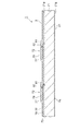
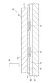
このような多光子吸収を利用する本実施形態に係るレーザ加工方法の原理について、図1〜図6を参照して説明する。図1に示すように、ウェハ状(平板状)の加工対象物1の表面3には、加工対象物1を切断するための切断予定ライン5がある。切断予定ライン5は直線状に延びた仮想線である。本実施形態に係るレーザ加工方法では、図2に示すように、多光子吸収が生じる条件で加工対象物1の内部に集光点Pを合わせてレーザ光Lを照射して改質領域7を形成する。なお、集光点Pとは、レーザ光Lが集光する箇所のことである。また、切断予定ライン5は、直線状に限らず曲線状であってもよいし、仮想線に限らず加工対象物1に実際に引かれた線であってもよい。
The principle of the laser processing method according to this embodiment using such multiphoton absorption will be described with reference to FIGS. As shown in FIG. 1, there is a scheduled
そして、レーザ光Lを切断予定ライン5に沿って(すなわち、図1の矢印A方向に)相対的に移動させることにより、集光点Pを切断予定ライン5に沿って移動させる。これにより、図3〜図5に示すように、改質領域7が切断予定ライン5に沿って加工対象物1の内部に形成され、この改質領域7が切断起点領域8となる。本実施形態に係るレーザ加工方法は、加工対象物1がレーザ光Lを吸収することにより加工対象物1を発熱させて改質領域7を形成するものではない。加工対象物1にレーザ光Lを透過させ加工対象物1の内部に多光子吸収を発生させて改質領域7を形成している。よって、加工対象物1の表面3ではレーザ光Lがほとんど吸収されないので、加工対象物1の表面3が溶融することはない。
Then, the condensing point P is moved along the
加工対象物1の内部に切断起点領域8を形成すると、この切断起点領域8を起点として割れが発生し易くなるため、図6に示すように、比較的小さな力で加工対象物1を切断することができる。よって、加工対象物1の表面3に不必要な割れを発生させることなく、加工対象物1を高精度に切断することが可能になる。
If the cutting
この切断起点領域8を起点とした加工対象物1の切断には、次の2通りが考えられる。1つは、切断起点領域8形成後、加工対象物1に人為的な力が印加されることにより、切断起点領域8を起点として加工対象物1が割れ、加工対象物1が切断される場合である。これは、例えば加工対象物1の厚さが大きい場合の切断である。人為的な力が印加されるとは、例えば、加工対象物1の切断起点領域8に沿って加工対象物1に曲げ応力やせん断応力を加えたり、加工対象物1に温度差を与えることにより熱応力を発生させたりすることである。他の1つは、切断起点領域8を形成することにより、切断起点領域8を起点として加工対象物1の断面方向(厚さ方向)に向かって自然に割れ、結果的に加工対象物1が切断される場合である。これは、例えば加工対象物1の厚さが小さい場合には、1列の改質領域7により切断起点領域8が形成されることで可能となり、加工対象物1の厚さが大きい場合には、厚さ方向に複数列形成された改質領域7により切断起点領域8が形成されることで可能となる。なお、この自然に割れる場合も、切断する箇所において、切断起点領域8が形成されていない部位に対応する部分の表面3上にまで割れが先走ることがなく、切断起点領域8を形成した部位に対応する部分のみを割断することができるので、割断を制御よくすることができる。近年、シリコンウェハ等の加工対象物1の厚さは薄くなる傾向にあるので、このような制御性のよい割断方法は大変有効である。
The following two types of cutting of the
さて、本実施形態に係るレーザ加工方法において、多光子吸収により形成される改質領域としては、次の(1)〜(4)の場合がある。 In the laser processing method according to the present embodiment, the modified regions formed by multiphoton absorption include the following cases (1) to (4).
(1)改質領域が1つ又は複数のクラックを含むクラック領域の場合
加工対象物(例えばガラスやLiTaO3からなる圧電材料)の内部に集光点を合わせて、集光点における電界強度が1×10⁸(W/cm2)以上で且つパルス幅が1μs以下の条件でレーザ光を照射する。このパルス幅の大きさは、多光子吸収を生じさせつつ加工対象物の表面に余計なダメージを与えずに、加工対象物の内部にのみクラック領域を形成できる条件である。これにより、加工対象物の内部には多光子吸収による光学的損傷という現象が発生する。この光学的損傷により加工対象物の内部に熱ひずみが誘起され、これにより加工対象物の内部にクラック領域が形成される。電界強度の上限値としては、例えば1×1012(W/cm2)である。パルス幅は例えば1ns〜200nsが好ましい。なお、多光子吸収によるクラック領域の形成は、例えば、第45回レーザ熱加工研究会論文集(1998年.12月)の第23頁〜第28頁の「固体レーザー高調波によるガラス基板の内部マーキング」に記載されている。
(1) In the case where the modified region is a crack region including one or a plurality of cracks, the focusing point is set inside the object to be processed (for example, a piezoelectric material made of glass or LiTaO 3 ), and the electric field strength at the focusing point is Irradiation with laser light is performed under conditions of 1 × 10 8 (W / cm 2 ) or more and a pulse width of 1 μs or less. The magnitude of this pulse width is a condition that allows a crack region to be formed only inside the workpiece without causing extra damage to the surface of the workpiece while causing multiphoton absorption. As a result, a phenomenon of optical damage due to multiphoton absorption occurs inside the workpiece. This optical damage induces thermal strain inside the workpiece, thereby forming a crack region inside the workpiece. The upper limit value of the electric field strength is, for example, 1 × 10 12 (W / cm 2 ). The pulse width is preferably 1 ns to 200 ns, for example. The formation of the crack region by multiphoton absorption is described in, for example, “Inside of glass substrate by solid-state laser harmonics” on pages 23-28 of the 45th Laser Thermal Processing Research Papers (December 1998). It is described in “Marking”.
本発明者は、電界強度とクラックの大きさとの関係を実験により求めた。実験条件は次ぎの通りである。 The inventor obtained the relationship between the electric field strength and the size of the cracks by experiment. The experimental conditions are as follows.
(A)加工対象物:パイレックス(登録商標)ガラス(厚さ700μm)
(B)レーザ
光源:半導体レーザ励起Nd:YAGレーザ
波長:1064nm
レーザ光スポット断面積:3.14×10⁻⁸cm2
発振形態:Qスイッチパルス
繰り返し周波数:100kHz
パルス幅:30ns
出力:出力<1mJ/パルス
レーザ光品質:TEM00
偏光特性:直線偏光
(C)集光用レンズ
レーザ光波長に対する透過率:60パーセント
(D)加工対象物が載置される載置台の移動速度:100mm/秒
(A) Workpiece: Pyrex (registered trademark) glass (thickness 700 μm)
(B) Laser
Light source: Semiconductor laser pumped Nd: YAG laser
Wavelength: 1064nm
Laser light spot cross-sectional area: 3.14 × 10 −8 cm 2
Oscillation form: Q switch pulse
Repeat frequency: 100 kHz
Pulse width: 30ns
Output: Output <1mJ / pulse
Laser light quality: TEM 00
Polarization characteristics: Linearly polarized light (C) Condensing lens
Transmittance with respect to laser beam wavelength: 60% (D) Moving speed of mounting table on which workpiece is mounted: 100 mm / second
なお、レーザ光品質がTEM00とは、集光性が高くレーザ光の波長程度まで集光可能を意味する。 Note that the laser light quality TEM 00 means that the light condensing performance is high and the light can be condensed up to the wavelength of the laser light.
図7は上記実験の結果を示すグラフである。横軸はピークパワー密度であり、レーザ光がパルスレーザ光なので電界強度はピークパワー密度で表される。縦軸は1パルスのレーザ光により加工対象物の内部に形成されたクラック部分(クラックスポット)の大きさを示している。クラックスポットが集まりクラック領域となる。クラックスポットの大きさは、クラックスポットの形状のうち最大の長さとなる部分の大きさである。グラフ中の黒丸で示すデータは集光用レンズ(C)の倍率が100倍、開口数(NA)が0.80の場合である。一方、グラフ中の白丸で示すデータは集光用レンズ(C)の倍率が50倍、開口数(NA)が0.55の場合である。ピークパワー密度が1011(W/cm2)程度から加工対象物の内部にクラックスポットが発生し、ピークパワー密度が大きくなるに従いクラックスポットも大きくなることが分かる。 FIG. 7 is a graph showing the results of the experiment. The horizontal axis represents the peak power density. Since the laser beam is a pulsed laser beam, the electric field strength is represented by the peak power density. The vertical axis represents the size of a crack portion (crack spot) formed inside the workpiece by one pulse of laser light. Crack spots gather to form a crack region. The size of the crack spot is the size of the portion having the maximum length in the shape of the crack spot. Data indicated by black circles in the graph is for the case where the magnification of the condenser lens (C) is 100 times and the numerical aperture (NA) is 0.80. On the other hand, the data indicated by the white circles in the graph is when the magnification of the condenser lens (C) is 50 times and the numerical aperture (NA) is 0.55. From the peak power density of about 10 11 (W / cm 2 ), it can be seen that a crack spot is generated inside the workpiece, and the crack spot increases as the peak power density increases.
次に、クラック領域形成による加工対象物の切断のメカニズムについて、図8〜図11を参照して説明する。図8に示すように、多光子吸収が生じる条件で加工対象物1の内部に集光点Pを合わせてレーザ光Lを照射して切断予定ラインに沿って内部にクラック領域9を形成する。クラック領域9は1つ又は複数のクラックを含む領域である。このように形成されたクラック領域9が切断起点領域となる。図9に示すように、クラック領域9を起点として(すなわち、切断起点領域を起点として)クラックがさらに成長し、図10に示すように、クラックが加工対象物1の表面3と裏面21とに到達し、図11に示すように、加工対象物1が割れることにより加工対象物1が切断される。加工対象物1の表面3と裏面21とに到達するクラックは自然に成長する場合もあるし、加工対象物1に力が印加されることにより成長する場合もある。
Next, the mechanism of cutting the workpiece by forming the crack region will be described with reference to FIGS. As shown in FIG. 8, the laser beam L is irradiated with the focusing point P inside the
(2)改質領域が溶融処理領域の場合
加工対象物(例えばシリコンのような半導体材料)の内部に集光点を合わせて、集光点における電界強度が1×10⁸(W/cm2)以上で且つパルス幅が1μs以下の条件でレーザ光を照射する。これにより加工対象物の内部は多光子吸収によって局所的に加熱される。この加熱により加工対象物の内部に溶融処理領域が形成される。溶融処理領域とは一旦溶融後再固化した領域や、まさに溶融状態の領域や、溶融状態から再固化する状態の領域であり、相変化した領域や結晶構造が変化した領域ということもできる。また、溶融処理領域とは単結晶構造、非晶質構造、多結晶構造において、ある構造が別の構造に変化した領域ということもできる。つまり、例えば、単結晶構造から非晶質構造に変化した領域、単結晶構造から多結晶構造に変化した領域、単結晶構造から非晶質構造及び多結晶構造を含む構造に変化した領域を意味する。加工対象物がシリコン単結晶構造の場合、溶融処理領域は例えば非晶質シリコン構造である。電界強度の上限値としては、例えば1×1012(W/cm2)である。パルス幅は例えば1ns〜200nsが好ましい。
(2) When the reforming region is a melt processing region The focusing point is set inside the object to be processed (for example, a semiconductor material such as silicon), and the electric field strength at the focusing point is 1 × 10 8 (W / cm 2). ) Irradiation with laser light is performed under the above conditions with a pulse width of 1 μs or less. As a result, the inside of the workpiece is locally heated by multiphoton absorption. By this heating, a melt processing region is formed inside the workpiece. The melt treatment region is a region once solidified after melting, a region in a molten state, or a region re-solidified from a molten state, and can also be referred to as a phase-changed region or a region in which the crystal structure has changed. The melt treatment region can also be said to be a region in which one structure is changed to another structure in a single crystal structure, an amorphous structure, or a polycrystalline structure. In other words, for example, a region changed from a single crystal structure to an amorphous structure, a region changed from a single crystal structure to a polycrystalline structure, or a region changed from a single crystal structure to a structure including an amorphous structure and a polycrystalline structure. To do. When the object to be processed has a silicon single crystal structure, the melt processing region has, for example, an amorphous silicon structure. The upper limit value of the electric field strength is, for example, 1 × 10 12 (W / cm 2 ). The pulse width is preferably 1 ns to 200 ns, for example.
本発明者は、シリコンウェハの内部で溶融処理領域が形成されることを実験により確認した。実験条件は次の通りである。 The inventor has confirmed through experiments that a melt-processed region is formed inside a silicon wafer. The experimental conditions are as follows.
(A)加工対象物:シリコンウェハ(厚さ350μm、外径4インチ)
(B)レーザ
光源:半導体レーザ励起Nd:YAGレーザ
波長:1064nm
レーザ光スポット断面積:3.14×10⁻⁸cm2
発振形態:Qスイッチパルス
繰り返し周波数:100kHz
パルス幅:30ns
出力:20μJ/パルス
レーザ光品質:TEM00
偏光特性:直線偏光
(C)集光用レンズ
倍率:50倍
N.A.:0.55
レーザ光波長に対する透過率:60パーセント
(D)加工対象物が載置される載置台の移動速度:100mm/秒
(A) Workpiece: silicon wafer (thickness 350 μm, outer diameter 4 inches)
(B) Laser
Light source: Semiconductor laser pumped Nd: YAG laser
Wavelength: 1064nm
Laser light spot cross-sectional area: 3.14 × 10 −8 cm 2
Oscillation form: Q switch pulse
Repeat frequency: 100 kHz
Pulse width: 30ns
Output: 20μJ / pulse
Laser light quality: TEM 00
Polarization characteristics: Linearly polarized light (C) Condensing lens
Magnification: 50 times
N. A. : 0.55
Transmittance with respect to laser beam wavelength: 60% (D) Moving speed of mounting table on which workpiece is mounted: 100 mm / second
図12は、上記条件でのレーザ加工により切断されたシリコンウェハの一部における断面の写真を表した図である。シリコンウェハ11の内部に溶融処理領域13が形成されている。なお、上記条件により形成された溶融処理領域13の厚さ方向の大きさは100μm程度である。
FIG. 12 is a view showing a photograph of a cross section of a part of a silicon wafer cut by laser processing under the above conditions. A
溶融処理領域13が多光子吸収により形成されたことを説明する。図13は、レーザ光の波長とシリコン基板の内部の透過率との関係を示すグラフである。ただし、シリコン基板の表面側と裏面側それぞれの反射成分を除去し、内部のみの透過率を示している。シリコン基板の厚さtが50μm、100μm、200μm、500μm、1000μmの各々について上記関係を示した。
The fact that the
例えば、Nd:YAGレーザの波長である1064nmにおいて、シリコン基板の厚さが500μm以下の場合、シリコン基板の内部ではレーザ光が80%以上透過することが分かる。図12に示すシリコンウェハ11の厚さは350μmであるので、多光子吸収による溶融処理領域13はシリコンウェハ11の中心付近、つまり表面から175μmの部分に形成される。この場合の透過率は、厚さ200μmのシリコンウェハを参考にすると、90%以上なので、レーザ光がシリコンウェハ11の内部で吸収されるのは僅かであり、ほとんどが透過する。このことは、シリコンウェハ11の内部でレーザ光が吸収されて、溶融処理領域13がシリコンウェハ11の内部に形成(つまりレーザ光による通常の加熱で溶融処理領域が形成)されたものではなく、溶融処理領域13が多光子吸収により形成されたことを意味する。多光子吸収による溶融処理領域の形成は、例えば、溶接学会全国大会講演概要第66集(2000年4月)の第72頁〜第73頁の「ピコ秒パルスレーザによるシリコンの加工特性評価」に記載されている。
For example, when the thickness of the silicon substrate is 500 μm or less at the wavelength of the Nd: YAG laser of 1064 nm, it can be seen that the laser light is transmitted by 80% or more inside the silicon substrate. Since the thickness of the
なお、シリコンウェハは、溶融処理領域によって形成される切断起点領域を起点として断面方向に向かって割れを発生させ、その割れがシリコンウェハの表面と裏面とに到達することにより、結果的に切断される。シリコンウェハの表面と裏面に到達するこの割れは自然に成長する場合もあるし、シリコンウェハに力が印加されることにより成長する場合もある。そして、切断起点領域からシリコンウェハの表面と裏面とに割れが自然に成長する場合には、切断起点領域を形成する溶融処理領域が溶融している状態から割れが成長する場合と、切断起点領域を形成する溶融処理領域が溶融している状態から再固化する際に割れが成長する場合とのいずれもある。ただし、どちらの場合も溶融処理領域はシリコンウェハの内部のみに形成され、切断後の切断面には、図12のように内部にのみ溶融処理領域が形成されている。このように、加工対象物の内部に溶融処理領域によって切断起点領域を形成すると、割断時、切断起点領域ラインから外れた不必要な割れが生じにくいので、割断制御が容易となる。 Note that a silicon wafer is cracked as a result of generating cracks in the cross-sectional direction starting from the cutting start region formed by the melt processing region and reaching the front and back surfaces of the silicon wafer. The The cracks that reach the front and back surfaces of the silicon wafer may grow naturally or may grow by applying force to the silicon wafer. And when a crack naturally grows from the cutting start region to the front and back surfaces of the silicon wafer, the case where the crack grows from a state where the melt treatment region forming the cutting starting region is melted, and the cutting starting region There are both cases where cracks grow when the solidified region is melted from the molten state. However, in either case, the melt processing region is formed only inside the silicon wafer, and the melt processing region is formed only inside the cut surface after cutting as shown in FIG. In this way, when the cutting start region is formed by the melt processing region inside the workpiece, unnecessary cracking off the cutting start region line is unlikely to occur during cleaving, so that cleaving control is facilitated.
(3)改質領域が溶融処理領域及び微小空洞の場合
加工対象物(例えばシリコンのような半導体材料)の内部に集光点を合わせて、集光点における電界強度が1×10⁸(W/cm2)以上で且つパルス幅が1μs以下の条件でレーザ光を照射する。これにより、加工対象物の内部には溶融処理領域と微小空洞とが形成される場合がある。なお、電界強度の上限値としては、例えば1×1012(W/cm2)である。パルス幅は例えば1ns〜200nsが好ましい。
(3) When the modified region is a melt-processed region and a microcavity The focusing point is set inside the object to be processed (for example, a semiconductor material such as silicon), and the electric field strength at the focusing point is 1 × 10 8 (W / Cm 2 ) or more and the pulse width is 1 μs or less. As a result, a melt processing region and a microcavity may be formed inside the workpiece. In addition, as an upper limit of an electric field strength, it is 1 * 10 < 12 > (W / cm < 2 >), for example. The pulse width is preferably 1 ns to 200 ns, for example.
図14に示すように、シリコンウェハ11の表面3側からレーザ光Lを入射させた場合、微小空洞14は、溶融処理領域13に対して裏面21側に形成される。図14では、溶融処理領域13と微小空洞14とが離れて形成されているが、溶融処理領域13と微小空洞14とが連続して形成される場合もある。つまり、多光子吸収によって溶融処理領域13及び微小空洞14が対になって形成される場合、微小空洞14は、溶融処理領域13に対してシリコンウェハ11におけるレーザ光入射面の反対側に形成されることになる。
As shown in FIG. 14, when the laser beam L is incident from the
このように、シリコンウェハ11にレーザ光Lを透過させシリコンウェハ11の内部に多光子吸収を発生させて溶融処理領域13を形成した場合に、それぞれの溶融処理領域13に対応した微小空洞14が形成される原理については必ずしも明らかではない。ここでは、溶融処理領域13及び微小空洞14が対になった状態で形成される原理に関して本発明者らが想定する2つの仮説を説明する。
As described above, when the
本発明者らが想定する第1の仮説は次の通りである。すなわち、図15に示すように、シリコンウェハ11の内部の集光点Pに焦点を合わせてレーザ光Lを照射すると、集光点Pの近傍に溶融処理領域13が形成される。従来は、このレーザ光Lとして、レーザ光源から照射されるレーザ光Lの中心部分の光(図15中、L4及びL5に相当する部分の光)を使用することとしていた。これは、レーザ光Lのガウシアン分布の中心部分を使用するためである。
The first hypothesis assumed by the present inventors is as follows. That is, as shown in FIG. 15, when the laser beam L is focused on the condensing point P inside the
本発明者らはレーザ光Lがシリコンウェハ11の表面3に与える影響をおさえるためにレーザ光Lを広げることとした。その一手法として、レーザ光源から照射されるレーザ光Lを所定の光学系でエキスパンドしてガウシアン分布の裾野を広げて、レーザ光Lの周辺部分の光(図15中、L1〜L3及びL6〜L8に相当する部分の光)のレーザ強度を相対的に上昇させることとした。このようにエキスパンドしたレーザ光Lをシリコンウェハ11に透過させると、既に説明したように集光点Pの近傍では溶融処理領域13が形成され、その溶融処理領域13に対応した部分に微小空洞14が形成される。つまり、溶融処理領域13と微小空洞14とはレーザ光Lの光軸(図15中の一点鎖線)に沿った位置に形成される。微小空洞14が形成される位置は、レーザ光Lの周辺部分の光(図15中、L1〜L3及びL6〜L8に相当する部分の光)が理論上集光される部分に相当する。
The inventors decided to broaden the laser light L in order to suppress the influence of the laser light L on the
このようにレーザ光Lの中心部分の光(図15中、L4及びL5に相当する部分の光)と、レーザ光Lの周辺部分の光(図15中、L1〜L3及びL6〜L8に相当する部分の光)とがそれぞれ集光される部分がシリコンウェハ11の厚さ方向において異なるのは、レーザ光Lを集光するレンズの球面収差によるものと考えられる。本発明者らが想定する第1の仮説は、この集光位置の差が何らかの影響を及ぼしているのではないかというものである。
As described above, light at the center of the laser light L (light corresponding to L4 and L5 in FIG. 15) and light at the peripheral portion of the laser light L (corresponding to L1 to L3 and L6 to L8 in FIG. 15). It is considered that the portions where the light is condensed in the thickness direction of the
本発明者らが想定する第2の仮説は、レーザ光Lの周辺部分の光(図15中、L1〜L3及びL6〜L8に相当する部分の光)が集光される部分は理論上のレーザ集光点であるから、この部分の光強度が高く微細構造変化が起こっているためにその周囲が実質的に結晶構造が変化していない微小空洞14が形成され、溶融処理領域13が形成されている部分は熱的な影響が大きく単純に溶解して再固化したというものである。
The second hypothesis assumed by the present inventors is that the portion where the light around the laser beam L (the portions corresponding to L1 to L3 and L6 to L8 in FIG. 15) is condensed is theoretically Since it is a laser condensing point, since the light intensity of this portion is high and a fine structure change has occurred, a
ここで、溶融処理領域13は上記(2)で述べた通りのものであるが、微小空洞14は、その周囲が実質的に結晶構造が変化していないものである。シリコンウェハ11がシリコン単結晶構造の場合には、微小空洞14の周囲はシリコン単結晶構造のままの部分が多い。
Here, the melt-processed
本発明者らは、シリコンウェハ11の内部で溶融処理領域13及び微小空洞14が形成されることを実験により確認した。実験条件は次の通りである。
The present inventors have confirmed through experiments that the
(A)加工対象物:シリコンウェハ(厚さ100μm)
(B)レーザ
光源:半導体レーザ励起Nd:YAGレーザ
波長:1064nm
繰り返し周波数:40kHz
パルス幅:30nsec
パルスピッチ:7μm
加工深さ:8μm
パルスエネルギー:50μJ/パルス
(C)集光用レンズ
NA:0.55
(D)加工対象物が載置される載置台の移動速度:280mm/sec
(A) Workpiece: silicon wafer (
(B) Laser Light source: Semiconductor laser excitation Nd: YAG laser Wavelength: 1064 nm
Repeat frequency: 40 kHz
Pulse width: 30nsec
Pulse pitch: 7μm
Processing depth: 8μm
Pulse energy: 50 μJ / pulse (C) Condensing lens NA: 0.55
(D) Movement speed of the mounting table on which the workpiece is placed: 280 mm / sec
図16は、上記条件でのレーザ加工により切断されたシリコンウェハ11の切断面の写真を表した図である。図16において(a)と(b)とは同一の切断面の写真を異なる縮尺で示したものである。同図に示すように、シリコンウェハ11の内部には、1パルスのレーザ光Lの照射により形成された溶融処理領域13及び微小空洞14の対が、切断面に沿って(すなわち、切断予定ラインに沿って)所定のピッチで形成されている。
FIG. 16 is a view showing a photograph of a cut surface of the
なお、図16に示す切断面の溶融処理領域13は、シリコンウェハ11の厚さ方向(図中の上下方向)の幅が13μm程度で、レーザ光Lを移動する方向(図中の左右方向)の幅が3μm程度である。また、微小空洞14は、シリコンウェハ11の厚さ方向の幅が7μm程度で、レーザ光Lを移動する方向の幅が1.3μm程度である。溶融処理領域13と微小空洞14との間隔は1.2μm程度である。
16 has a width of about 13 μm in the thickness direction (vertical direction in the figure) of the
(4)改質領域が屈折率変化領域の場合
加工対象物(例えばガラス)の内部に集光点を合わせて、集光点における電界強度が1×10⁸(W/cm2)以上で且つパルス幅が1ns以下の条件でレーザ光を照射する。パルス幅を極めて短くして、多光子吸収を加工対象物の内部に起こさせると、多光子吸収によるエネルギーが熱エネルギーに転化せずに、加工対象物の内部にはイオン価数変化、結晶化又は分極配向等の永続的な構造変化が誘起されて屈折率変化領域が形成される。電界強度の上限値としては、例えば1×1012(W/cm2)である。パルス幅は例えば1ns以下が好ましく、1ps以下がさらに好ましい。多光子吸収による屈折率変化領域の形成は、例えば、第42回レーザ熱加工研究会論文集(1997年.11月)の第105頁〜第111頁の「フェムト秒レーザー照射によるガラス内部への光誘起構造形成」に記載されている。
(4) When the modified region is a refractive index changing region The focusing point is set inside the object to be processed (for example, glass), and the electric field strength at the focusing point is 1 × 10 8 (W / cm 2 ) or more and Laser light is irradiated under the condition that the pulse width is 1 ns or less. When the pulse width is made extremely short and multiphoton absorption occurs inside the workpiece, the energy due to the multiphoton absorption is not converted into thermal energy, and the ion valence change and crystallization occur inside the workpiece. Alternatively, a permanent structural change such as polarization orientation is induced to form a refractive index change region. The upper limit value of the electric field strength is, for example, 1 × 10 12 (W / cm 2 ). For example, the pulse width is preferably 1 ns or less, and more preferably 1 ps or less. The formation of the refractive index changing region by multiphoton absorption is described in, for example, “The Femtosecond Laser Irradiation to the Inside of Glass” on pages 105 to 111 of the 42nd Laser Thermal Processing Research Institute Proceedings (November 1997). Photo-induced structure formation ”.
以上、多光子吸収により形成される改質領域として(1)〜(4)の場合を説明したが、ウェハ状の加工対象物の結晶構造やその劈開性などを考慮して切断起点領域を次のように形成すれば、その切断起点領域を起点として、より一層小さな力で、しかも精度良く加工対象物を切断することが可能になる。 As described above, the cases of (1) to (4) have been described as the modified regions formed by multiphoton absorption. However, the cutting starting region is determined in consideration of the crystal structure of the wafer-like workpiece and its cleavage. If it forms in this way, it will become possible to cut | disconnect a process target object with much smaller force from the cutting | disconnection starting point area | region as a starting point, and still more accurately.
すなわち、シリコンなどのダイヤモンド構造の単結晶半導体からなる基板の場合は、(111)面(第1劈開面)や(110)面(第2劈開面)に沿った方向に切断起点領域を形成するのが好ましい。また、GaAsなどの閃亜鉛鉱型構造のIII−V族化合物半導体からなる基板の場合は、(110)面に沿った方向に切断起点領域を形成するのが好ましい。さらに、サファイア(Al2O3)などの六方晶系の結晶構造を有する基板の場合は、(0001)面(C面)を主面として(1120)面(A面)或いは(1100)面(M面)に沿った方向に切断起点領域を形成するのが好ましい。 That is, in the case of a substrate made of a single crystal semiconductor having a diamond structure such as silicon, the cutting start region is formed in a direction along the (111) plane (first cleavage plane) or the (110) plane (second cleavage plane). Is preferred. In the case of a substrate made of a zinc-blende-type III-V group compound semiconductor such as GaAs, it is preferable to form the cutting start region in the direction along the (110) plane. Furthermore, in the case of a substrate having a hexagonal crystal structure such as sapphire (Al 2 O 3 ), the (1120) plane (A plane) or (1100) plane ( It is preferable to form the cutting start region in a direction along the (M plane).
なお、上述した切断起点領域を形成すべき方向(例えば、単結晶シリコン基板における(111)面に沿った方向)、或いは切断起点領域を形成すべき方向に直交する方向に沿って基板にオリエンテーションフラットを形成すれば、そのオリエンテーションフラットを基準とすることで、切断起点領域を形成すべき方向に沿った切断起点領域を容易且つ正確に基板に形成することが可能になる。 Note that the orientation flat is formed on the substrate along the direction in which the above-described cutting start region is to be formed (for example, the direction along the (111) plane in the single crystal silicon substrate) or the direction perpendicular to the direction in which the cutting start region is to be formed. By using the orientation flat as a reference, it is possible to easily and accurately form the cutting start area along the direction in which the cutting start area is to be formed on the substrate.
[第1実施形態]
次に、第1実施形態に係るレーザ加工方法について説明する。なお、図19〜図22は、図18に示すXIX−XIX線に沿っての部分断面図である。
[First Embodiment]
Next, the laser processing method according to the first embodiment will be described. 19 to 22 are partial cross-sectional views along the line XIX-XIX shown in FIG.
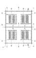
図17に示すように、加工対象物1は、タンタル酸リチウム等の圧電基板であり、その表面(一方の面)3には、多数のSAWフィルタ素子51がフォトリソグラフィ技術によって形成されている。各SAWフィルタ素子51は、図18に示すように、ITD電極52を表面波の伝搬方向に並設させたトランスバーサル型のフィルタであり、各ITD電極52は、細線状の金属膜53によって並列に接続されている。また、各SAWフィルタ素子51は、細線状の金属膜54によって矩形状に仕切られており、この金属膜54に対しては、ITD電極52を接続する金属膜53の一部が近接配置されている。
As shown in FIG. 17, the
このような電極構成を採用することで、加工対象物1が急激な温度変化にさらされて焦電効果により焦電荷が発生しても、金属膜53を介して焦電荷が瞬時に移動するため、ITD電極52の放電破壊を防止することができる。
By adopting such an electrode configuration, even if the
以上のように構成された加工対象物1を以下のようにして金属膜54に沿って格子状に切断する。まず、加工対象物1の金属膜54上に切断予定ライン5を設定し(図18参照)、この加工対象物1に対する切断予定ライン5の位置データを記憶手段(例えば、コンピュータのメモリ等)に保存する。
The
続いて、ダイシングソーを用いて加工対象物1の表面3に溝を形成する(溝形成工程)。すなわち、図19に示すように、加工対象物1の裏面(他方の面)21に保護フィルム56を貼り付けて、表面3を上方に向けて加工対象物1をダイシングソーの載置台57上に真空チャック等で固定する。そして、記憶手段に記憶された切断予定ライン5の位置データに基づいて加工対象物1に対してブレード58を相対移動させ、加工対象物1の表面3に溝を形成する。なお、ブレード58は、例えば、刃先がダイヤモンドにより形成された回転ブレードである。
Subsequently, a groove is formed on the
これにより、加工対象物1の表面3には、図20に示すように、切断予定ライン5に沿って所定深さの溝59が形成される。また、同時に加工対象物1の表面3から金属膜54と金属膜53の一部とが除去されて、SAWフィルタ素子51について所望の動作が得られることになる。
As a result, a
溝形成工程の後、レーザ加工装置を用いて加工対象物1の内部に切断起点領域を形成する(切断起点領域形成工程)。すなわち、図21に示すように、加工対象物1の裏面21から保護フィルム56を取り除き、加工対象物1の表面3に保護フィルム61を貼り付けて、裏面21を上方に向けて加工対象物1をレーザ加工装置の載置台62上に真空チャック等で固定する。そして、裏面21をレーザ光入射面として加工対象物1の内部に集光点Pを合わせて、上述した多光子吸収が生じる条件でレーザ光Lを照射し、同時に、記憶手段に記憶された切断予定ライン5の位置データに基づいて加工対象物1に対して集光点Pを相対移動させる。
After the groove forming step, a cutting starting point region is formed inside the
これにより、加工対象物1の裏面21と溝59の底面59aとの間の切断予定部分60には、切断予定ライン5に沿って改質領域7により切断起点領域8が形成される。このように、溝形成工程と切断起点領域形成工程とにおいて切断予定ライン1についての同じ位置データを使用することで、溝59と切断起点領域8との位置ずれを防止することができる。
As a result, the cutting
切断起点領域形成工程の後、フィルム拡張装置を用いて切断予定部分60にストレスを生じさせる(ストレス印加工程)。すなわち、図22に示すように、加工対象物1の表面3から保護フィルム61を取り除き、加工対象物1の裏面21に拡張フィルム(拡張可能部材)63を貼り付けて、拡張フィルム63を外方側にエキスパンドし、切断予定部分60に引張応力やせん断応力等のストレスを生じさせる。
After the cutting start region forming step, stress is generated in the planned cutting
これにより、切断起点領域8を起点として割れ64が発生し、この割れ64が溝59の底面59aと加工対象物1の裏面21とに到達して、加工対象物1が切断予定ライン5に沿って複数のチップ66に切断される。なお、拡張フィルム63の拡張に伴い各チップ66が互いに離間するため、各チップ66を容易且つ確実にピックアップすることが可能になる。
As a result, a
以上のように、第1実施形態に係るレーザ加工方法においては、切断予定ライン5に沿って加工対象物1の表面3に溝59を形成した後に、切断予定ライン5に沿って加工対象物1の内部に改質領域7による切断起点領域8を形成する。そのため、例えば、加工対象物1の表面3に溝59のみを形成したものに比べ、より小さな力で拡張フィルム63を拡張させて加工対象物1を個々のチップ66に切断することができる。したがって、上述したタンタル酸リチウムその他の酸化物単結晶(水晶、ニオブ酸リチウム、サファイア等)或いは光透過性セラミックス等、硬度の高い加工対象物1であっても、ブレード58によりフルカットする方法や、加工対象物1の表面3に溝59のみを形成して割断する方法に比べ、切断予定ライン5に沿って加工対象物1を効率良く切断することが可能になる。
As described above, in the laser processing method according to the first embodiment, after forming the
また、溝形成工程においては、ブレード58により溝59を形成するため、溝59の底面59aに多数のマイクロクラックが発生し得る。そのため、切断起点領域形成工程において加工対象物1の表面3側からレーザ光Lを照射すると、マイクロクラックにより散乱等が生じ、加工対象物1の内部にレーザ光Lを効率良く集光することができない。しかしながら、本実施形態のレーザ加工方法においては、加工対象物1の裏面21側から加工対象物1の内部にレーザ光Lを集光させるため、形成した溝59の形状に拘わらず、切断起点領域8を加工対象物1の内部に確実に形成することができる。なお、切断起点領域8を起点とした割れ64は前述のマイクロクラックと連結し易くなるため、当該マイクロクラックは、割れ64が溝59の底面59a内に確実に収まるのを促進させる。
In the groove forming step, since the
さらに、溝形成工程及び切断起点領域形成工程の後にストレス印加工程を備えているため、溝59の深さや幅を小さくすることが可能となる。したがって、加工対象物1の切断時間のより一層の短縮化や、溝59の形成による切削屑の減少化を達成できる。しかも、溝59の幅を小さくすることで、加工対象物1から得られるチップ66の数を増加させることができる。
Furthermore, since the stress applying step is provided after the groove forming step and the cutting start region forming step, the depth and width of the
[第2実施形態]
次に、第2実施形態に係るレーザ加工方法について説明する。なお、図24〜図28は、図23に示すXXIV−XXIV線に沿っての部分断面図である。
[Second Embodiment]
Next, a laser processing method according to the second embodiment will be described. 24 to 28 are partial cross-sectional views along the line XXIV-XXIV shown in FIG.
図23及び図24に示すように、加工対象物1は、シリコンからなる基板71と、複数の機能素子72を含んで基板71の表面71aに形成された積層部73と、基板71の裏面71bに形成されたダイボンド樹脂層74とを備えている。ダイボンド樹脂層74は、紫外線や赤外線等の電磁波の照射により或いは加熱により、粘着性を有するようになるもの又は粘着度を増大させるものであり、チップパッケージに固定する際の接着剤として機能する。なお、基板71の裏面71bには、ダイボンド樹脂層74に代わって、金やアルミニウム等の金属膜或いは有機膜が形成される場合もある。
As shown in FIGS. 23 and 24, the
機能素子72は、基板71の表面71aに積層された層間絶縁膜76と、層間絶縁膜76上に配置された配線層77と、配線層77を覆うように層間絶縁膜76上に積層された層間絶縁膜78と、層間絶縁膜78上に配置された配線層79とを有している。配線層77と基板71とは、層間絶縁膜76を貫通する導電性プラグ81によって電気的に接続され、配線層79と配線層77とは、層間絶縁膜78を貫通する導電性プラグ82によって電気的に接続されている。
The
なお、機能素子72は、基板71のオリエンテーションフラット71cに平行な方向及び垂直な方向にマトリックス状に多数形成されているが、層間絶縁膜76,78は、基板71の表面71a全体を覆うように隣り合う機能素子72,72間に渡って形成されている。
A large number of
以上のように構成された加工対象物1を以下のようにして機能素子72毎に切断する。まず、加工対象物1に対し、隣り合う機能素子72,72間を通るように切断予定ライン5を格子状に設定し(図23参照)、この加工対象物1に対する切断予定ライン5の位置データを記憶手段に保存する。
The
続いて、ダイシングソーを用いて加工対象物1の裏面(一方の面)21に溝を形成する(溝形成工程)。すなわち、図25に示すように、加工対象物1の表面(他方の面)3に保護フィルム56を貼り付けて、裏面21を上方に向けて加工対象物1をダイシングソーの載置台57上に真空チャック等で固定する。そして、記憶手段に記憶された切断予定ライン5の位置データに基づいて加工対象物1に対してブレード58を相対移動させ、加工対象物1の裏面21に溝を形成する。これにより、加工対象物1の裏面21には、図26に示すように、切断予定ライン5に沿って所定深さの溝59が形成される。なお、保護フィルム56の代えて、加工対象物1の表面3に、ガラスや樹脂等からなるプレート状の保護部材を両面テープや粘着剤等により取り付けてもよい。
Subsequently, a groove is formed on the back surface (one surface) 21 of the
溝形成工程の後、レーザ加工装置を用いて加工対象物1の内部に切断起点領域を形成する(切断起点領域形成工程)。すなわち、図27に示すように、加工対象物1の表面3から保護フィルム56を取り除き、加工対象物1の裏面21に拡張フィルム(拡張可能部材)63を貼り付けて、表面3を上方に向けて加工対象物1をレーザ加工装置の載置台62上に真空チャック等で固定する。そして、表面3をレーザ光入射面として加工対象物1の内部に集光点Pを合わせて、上述した多光子吸収が生じる条件でレーザ光Lを照射し、同時に、記憶手段に記憶された切断予定ライン5の位置データに基づいて加工対象物1に対して集光点Pを相対移動させる。なお、層間絶縁膜76,78は、レーザ光Lに対して透過性を有する材料(SiO2やSiN等)からなっている。
After the groove forming step, a cutting starting point region is formed inside the
これにより、加工対象物1の表面3と溝59の底面59aとの間の切断予定部分60には、切断予定ライン5に沿って改質領域7により切断起点領域8が形成される。このように、溝形成工程と切断起点領域形成工程とにおいて切断予定ライン1についての同じ位置データを使用することで、溝59と切断起点領域8との位置ずれを防止することができる。なお、基板71はシリコンからなる半導体基板であるため、改質領域7は溶融処理領域である。
As a result, the cutting
切断起点領域形成工程の後、フィルム拡張装置を用いて切断予定部分60にストレスを生じさせる(ストレス印加工程)。すなわち、図28に示すように、加工対象物1の裏面21に貼り付けられた拡張フィルム63を外方側にエキスパンドし、切断予定部分60に引張応力やせん断応力等のストレスを生じさせる。
After the cutting start region forming step, stress is generated in the planned cutting
これにより、切断起点領域8を起点として割れ64が発生し、この割れ64が溝59の底面59aと加工対象物1の表面3とに到達して、加工対象物1が切断予定ライン5に沿って複数のチップ66に切断される。なお、拡張フィルム63の拡張に伴い各チップ66が互いに離間するため、各チップ66を容易且つ確実にピックアップすることが可能になる。
As a result, a
以上のように、第2実施形態に係るレーザ加工方法においては、切断予定ライン5に沿って加工対象物1の裏面21に溝59を形成した後に、切断予定ライン5に沿って加工対象物1の内部に改質領域7による切断起点領域8を形成する。したがって、第1実施形態に係るレーザ加工方法と同様の理由から、硬度の高い加工対象物1であっても、ブレード58によりフルカットする方法や、加工対象物1の裏面21に溝59のみを形成して割断する方法に比べ、切断予定ライン5に沿って加工対象物1を効率良く切断することが可能になる。
As described above, in the laser processing method according to the second embodiment, the
また、ストレス印加工程においては、切断予定ライン5に沿って溝59が形成された加工対象物1の裏面21に拡張フィルム63を貼り付けて、その拡張フィルム63を拡張させるため、加工対象物1には溝59が広げられるように力が作用し、その結果、切断予定ライン5に沿って形成された切断起点領域8との協働により、加工対象物1を切断予定ライン5に沿って容易に切断することが可能になる。
In addition, in the stress application step, the
本発明は上記実施形態には限定されない。例えば、第1及び第2実施形態に係るレーザ加工方法は、加工対象物1の内部で多光子吸収を生じさせて改質領域7を形成した場合であったが、加工対象物1の内部で多光子吸収と同等の光吸収を生じさせて改質領域7を形成することができる場合もある。
The present invention is not limited to the above embodiment. For example, the laser processing method according to the first and second embodiments is a case where the modified
また、第2実施形態に係るレーザ加工方法は、シリコンからなる基板71の内部に改質領域7として溶融処理領域を形成する場合であったが、改質領域7として溶融処理領域及び微小空洞を形成してもよい。
In the laser processing method according to the second embodiment, the melt processing region is formed as the modified
また、第1及び第2実施形態に係るレーザ加工方法の溝形成工程ではブレード58により溝59を形成したが、エッチング等、他の方法により溝59を形成してもよい。また、加工対象物1の厚さや硬度、溝59の深さ等によっては、切断起点領域8の形成と同時に(或いは、その後に)、切断起点領域8を起点として割れ64が自然に発生して加工対象物1が切断される場合がある。このような場合には、拡張フィルム63を拡張させるといったストレス印加工程が不要になるため、加工対象物1の更に効率の良い切断が可能となる。
In the groove forming step of the laser processing method according to the first and second embodiments, the
また、溝形成工程及び切断起点領域形成工程の後にストレス印加工程を備える場合でも、切断起点領域8を起点として自然に発生する割れ64を加工対象物1の裏面21又は溝59の底面59aのいずれか一方に到達させてもよい。このような制御は、例えば、切断予定部分60の厚さ方向における中心位置から裏面21又は底面59aのいずれか一方に偏倚させて改質領域7を形成することで可能になる。特に、割れ64を拡張フィルム63側の面に到達させると(加工対象物1の表面3側に拡張フィルム63を貼り付ける場合もある)、拡張フィルム63の拡張による加工対象物1の割断精度をより一層向上させることができる。
Even when the stress applying step is provided after the groove forming step and the cutting start region forming step, the
なお、「切断予定部分60の厚さ方向における中心位置から加工対象物1の裏面21側に偏倚させて改質領域7を形成する」とは、切断起点領域8を構成する改質領域7が、切断予定部分60の厚さ方向における厚さ(すなわち、裏面21と底面59aとの距離)の半分の位置から裏面21側に偏倚して形成されることを意味する。つまり、切断予定部分60の厚さ方向における改質領域7の幅の中心位置が、切断予定部分60の厚さ方向における中心位置から裏面21側に偏倚して位置している場合を意味し、改質領域7の全ての部分が切断予定部分60の厚さ方向における中心位置に対して裏面21側に位置している場合のみに限る意味ではない。溝59の底面59a側に偏倚させて改質領域7を形成する場合についても同様である。
Note that “the modified
また、溝形成工程後の加工対象物1において、切断予定部分60の厚さ方向における厚さが比較的厚い場合には、図29に示すように、切断起点領域形成工程おいて、切断予定ライン5に沿って切断予定部分60に改質領域7を複数列形成することが好ましい。これは、拡張フィルム63の拡張により、加工対象物1を切断予定ライン5に沿って容易に切断することが可能になると共に、加工対象物1の積層部73を切断予定ライン5に沿ってより一層精度良く切断することが可能になるからである。
In addition, in the
1…加工対象物、3…表面、5…切断予定ライン、7…改質領域、8…切断起点領域、11…シリコンウェハ(半導体基板)、13…溶融処理領域、14…微小空洞、21…裏面、59…溝、59a…底面、60…切断予定部分、63…拡張フィルム(拡張可能部材)、64…割れ、L…レーザ光、P…集光点。
DESCRIPTION OF
Claims (8)
前記溝を形成した後、前記加工対象物の他方の面をレーザ光入射面として前記加工対象物の内部に集光点を合わせてレーザ光を照射し、前記加工対象物の内部に改質領域を形成し、この改質領域によって、前記切断予定ラインに沿って前記レーザ光入射面から所定距離内側に切断起点領域を形成する工程とを備えることを特徴とするレーザ加工方法。 Forming a groove along a cutting line of the workpiece on one surface of the wafer-like workpiece;
After forming the groove, the other surface of the object to be processed is a laser beam incident surface, and a laser beam is irradiated with the focusing point inside the object to be processed, and a modified region is formed inside the object to be processed. And forming a cutting start region by a predetermined distance inside the laser light incident surface along the planned cutting line by the modified region.
前記溝を形成した後、前記加工対象物の前記一方の面に拡張可能部材を取り付ける工程と、
前記拡張可能部材を取り付けた後、前記加工対象物の他方の面をレーザ光入射面として前記加工対象物の内部に集光点を合わせてレーザ光を照射し、前記加工対象物の内部に改質領域を形成し、この改質領域によって、前記切断予定ラインに沿って前記レーザ光入射面から所定距離内側に切断起点領域を形成する工程と、
切断起点領域を形成した後、前記加工対象物の前記一方の面に取り付けられた拡張可能部材を拡張させることで、前記切断予定部分にストレスを生じさ、前記加工対象物を切断予定ラインに沿って切断する工程とを備えることを特徴とするレーザ加工方法。 Forming a groove along a cutting line of the workpiece on one surface of the wafer-like workpiece;
Attaching the expandable member to the one surface of the workpiece after forming the groove;
After attaching the expandable member, the other surface of the object to be processed is set as a laser light incident surface, and the laser beam is irradiated with a focusing point inside the object to be processed, and the inside of the object to be processed is modified. Forming a material region, and forming a cutting start region inside the predetermined distance from the laser light incident surface along the planned cutting line by the modified region;
After forming the cutting start region, by expanding the expandable member attached to the one surface of the workpiece, stress is generated in the planned cutting portion, and the processing target is cut along the planned cutting line. And a step of cutting.
Priority Applications (1)
| Application Number | Priority Date | Filing Date | Title |
|---|---|---|---|
| JP2004157965A JP2005012203A (en) | 2003-05-29 | 2004-05-27 | Laser machining method |
Applications Claiming Priority (2)
| Application Number | Priority Date | Filing Date | Title |
|---|---|---|---|
| JP2003152880 | 2003-05-29 | ||
| JP2004157965A JP2005012203A (en) | 2003-05-29 | 2004-05-27 | Laser machining method |
Publications (1)
| Publication Number | Publication Date |
|---|---|
| JP2005012203A true JP2005012203A (en) | 2005-01-13 |
Family
ID=34106783
Family Applications (1)
| Application Number | Title | Priority Date | Filing Date |
|---|---|---|---|
| JP2004157965A Pending JP2005012203A (en) | 2003-05-29 | 2004-05-27 | Laser machining method |
Country Status (1)
| Country | Link |
|---|---|
| JP (1) | JP2005012203A (en) |
Cited By (21)
| Publication number | Priority date | Publication date | Assignee | Title |
|---|---|---|---|---|
| JP2006086509A (en) * | 2004-08-17 | 2006-03-30 | Denso Corp | Method for dividing semiconductor substrate |
| JP2007087973A (en) * | 2005-09-16 | 2007-04-05 | Rohm Co Ltd | Manufacture of nitride semiconductor device, method for manufacturing nitride semiconductor device, and nitride semiconductor light-emitting device obtained by the same |
| JP2007134454A (en) * | 2005-11-09 | 2007-05-31 | Toshiba Corp | Method of manufacturing semiconductor device |
| JP2007235008A (en) * | 2006-03-03 | 2007-09-13 | Denso Corp | Dividing method for wafer, and chip |
| JP2008078440A (en) * | 2006-09-22 | 2008-04-03 | Dowa Holdings Co Ltd | Light-emitting element, and its manufacturing method |
| JP2009290148A (en) * | 2008-06-02 | 2009-12-10 | Disco Abrasive Syst Ltd | Method of dividing wafer |
| JP2010239163A (en) * | 2003-07-18 | 2010-10-21 | Hamamatsu Photonics Kk | Semiconductor chip |
| JP2012028734A (en) * | 2010-06-24 | 2012-02-09 | Toshiba Mach Co Ltd | Dicing method |
| JP2012146724A (en) * | 2011-01-07 | 2012-08-02 | Disco Abrasive Syst Ltd | Processing method of optical device wafer and optical device |
| JP2012199399A (en) * | 2011-03-22 | 2012-10-18 | Panasonic Corp | Laser processing method and laser processing apparatus |
| WO2013039150A1 (en) * | 2011-09-16 | 2013-03-21 | 浜松ホトニクス株式会社 | Laser machining method |
| WO2013039012A1 (en) * | 2011-09-16 | 2013-03-21 | 浜松ホトニクス株式会社 | Laser machining method and laser machining device |
| US20130082358A1 (en) * | 2010-03-05 | 2013-04-04 | Disco Corporation | Single crystal substrate with multilayer film, manufacturing method for single crystal substrate with multilayer film, and element manufacturing method |
| WO2013141032A1 (en) * | 2012-03-23 | 2013-09-26 | シャープ株式会社 | Semiconductor light emitting element, method for manufacturing semiconductor light emitting element, semiconductor light emitting device, and substrate |
| JP2015005558A (en) * | 2013-06-19 | 2015-01-08 | 株式会社ディスコ | Wafer processing method |
| JP2015005648A (en) * | 2013-06-21 | 2015-01-08 | 株式会社ディスコ | Wafer processing method |
| JP2015207604A (en) * | 2014-04-17 | 2015-11-19 | 株式会社ディスコ | Wafer processing method |
| CN106601876A (en) * | 2015-10-19 | 2017-04-26 | 映瑞光电科技(上海)有限公司 | LED chip structure and manufacturing method thereof |
| US20170190000A1 (en) * | 2005-09-08 | 2017-07-06 | Imra America, Inc. | Transparent material processing with an ultrashort pulse laser |
| JP2018098379A (en) * | 2016-12-14 | 2018-06-21 | 株式会社ディスコ | Interposer manufacturing method |
| WO2018230297A1 (en) * | 2017-06-15 | 2018-12-20 | 株式会社デンソー | Semiconductor device and method for manufacturing same |
-
2004
- 2004-05-27 JP JP2004157965A patent/JP2005012203A/en active Pending
Cited By (27)
| Publication number | Priority date | Publication date | Assignee | Title |
|---|---|---|---|---|
| JP2010239163A (en) * | 2003-07-18 | 2010-10-21 | Hamamatsu Photonics Kk | Semiconductor chip |
| US8852698B2 (en) | 2003-07-18 | 2014-10-07 | Hamamatsu Photonics K.K. | Laser beam machining method, laser beam machining apparatus, and laser beam machining product |
| JP2006086509A (en) * | 2004-08-17 | 2006-03-30 | Denso Corp | Method for dividing semiconductor substrate |
| US20170190000A1 (en) * | 2005-09-08 | 2017-07-06 | Imra America, Inc. | Transparent material processing with an ultrashort pulse laser |
| JP2007087973A (en) * | 2005-09-16 | 2007-04-05 | Rohm Co Ltd | Manufacture of nitride semiconductor device, method for manufacturing nitride semiconductor device, and nitride semiconductor light-emitting device obtained by the same |
| JP2007134454A (en) * | 2005-11-09 | 2007-05-31 | Toshiba Corp | Method of manufacturing semiconductor device |
| JP2007235008A (en) * | 2006-03-03 | 2007-09-13 | Denso Corp | Dividing method for wafer, and chip |
| JP2008078440A (en) * | 2006-09-22 | 2008-04-03 | Dowa Holdings Co Ltd | Light-emitting element, and its manufacturing method |
| JP2009290148A (en) * | 2008-06-02 | 2009-12-10 | Disco Abrasive Syst Ltd | Method of dividing wafer |
| US20130082358A1 (en) * | 2010-03-05 | 2013-04-04 | Disco Corporation | Single crystal substrate with multilayer film, manufacturing method for single crystal substrate with multilayer film, and element manufacturing method |
| JP2012028734A (en) * | 2010-06-24 | 2012-02-09 | Toshiba Mach Co Ltd | Dicing method |
| JP2012146724A (en) * | 2011-01-07 | 2012-08-02 | Disco Abrasive Syst Ltd | Processing method of optical device wafer and optical device |
| JP2012199399A (en) * | 2011-03-22 | 2012-10-18 | Panasonic Corp | Laser processing method and laser processing apparatus |
| WO2013039012A1 (en) * | 2011-09-16 | 2013-03-21 | 浜松ホトニクス株式会社 | Laser machining method and laser machining device |
| JP2013063453A (en) * | 2011-09-16 | 2013-04-11 | Hamamatsu Photonics Kk | Laser machining method |
| WO2013039150A1 (en) * | 2011-09-16 | 2013-03-21 | 浜松ホトニクス株式会社 | Laser machining method |
| TWI594832B (en) * | 2011-09-16 | 2017-08-11 | Hamamatsu Photonics Kk | Laser processing method |
| WO2013141032A1 (en) * | 2012-03-23 | 2013-09-26 | シャープ株式会社 | Semiconductor light emitting element, method for manufacturing semiconductor light emitting element, semiconductor light emitting device, and substrate |
| JPWO2013141032A1 (en) * | 2012-03-23 | 2015-08-03 | シャープ株式会社 | Semiconductor light emitting device, method for manufacturing semiconductor light emitting device, semiconductor light emitting device, and substrate |
| JP2015005558A (en) * | 2013-06-19 | 2015-01-08 | 株式会社ディスコ | Wafer processing method |
| JP2015005648A (en) * | 2013-06-21 | 2015-01-08 | 株式会社ディスコ | Wafer processing method |
| JP2015207604A (en) * | 2014-04-17 | 2015-11-19 | 株式会社ディスコ | Wafer processing method |
| CN106601876A (en) * | 2015-10-19 | 2017-04-26 | 映瑞光电科技(上海)有限公司 | LED chip structure and manufacturing method thereof |
| JP2018098379A (en) * | 2016-12-14 | 2018-06-21 | 株式会社ディスコ | Interposer manufacturing method |
| WO2018230297A1 (en) * | 2017-06-15 | 2018-12-20 | 株式会社デンソー | Semiconductor device and method for manufacturing same |
| JP2019004053A (en) * | 2017-06-15 | 2019-01-10 | 株式会社デンソー | Semiconductor device and manufacturing method thereof |
| US11145515B2 (en) | 2017-06-15 | 2021-10-12 | Denso Corporation | Manufacturing method of semiconductor device with attached film |
Similar Documents
| Publication | Publication Date | Title |
|---|---|---|
| JP4907984B2 (en) | Laser processing method and semiconductor chip | |
| JP4536407B2 (en) | Laser processing method and object to be processed | |
| JP4954653B2 (en) | Laser processing method | |
| JP4829781B2 (en) | Laser processing method and semiconductor chip | |
| JP5138219B2 (en) | Laser processing method | |
| JP4198123B2 (en) | Laser processing method | |
| JP4917257B2 (en) | Laser processing method | |
| JP4200177B2 (en) | Laser processing method and semiconductor device | |
| JP4781661B2 (en) | Laser processing method | |
| JP4908652B2 (en) | Substrate on which cutting start region is formed | |
| JP4776994B2 (en) | Processing object cutting method | |
| JP4907965B2 (en) | Laser processing method | |
| JP4762653B2 (en) | Laser processing method and laser processing apparatus | |
| JP2005012203A (en) | Laser machining method | |
| JP5322418B2 (en) | Laser processing method and laser processing apparatus | |
| WO2008035679A1 (en) | Laser processing method and laser processing apparatus | |
| JP5177992B2 (en) | Processing object cutting method | |
| JP5122161B2 (en) | Processing object cutting method | |
| JP2004351477A (en) | Laser beam machining method |