JP5268232B2 - Optical device - Google Patents
Optical device Download PDFInfo
- Publication number
- JP5268232B2 JP5268232B2 JP2006108860A JP2006108860A JP5268232B2 JP 5268232 B2 JP5268232 B2 JP 5268232B2 JP 2006108860 A JP2006108860 A JP 2006108860A JP 2006108860 A JP2006108860 A JP 2006108860A JP 5268232 B2 JP5268232 B2 JP 5268232B2
- Authority
- JP
- Japan
- Prior art keywords
- optical filter
- electrode
- piezoelectric member
- filter
- dust
- Prior art date
- Legal status (The legal status is an assumption and is not a legal conclusion. Google has not performed a legal analysis and makes no representation as to the accuracy of the status listed.)
- Expired - Fee Related
Links
Images


Landscapes
- Blocking Light For Cameras (AREA)
- Camera Bodies And Camera Details Or Accessories (AREA)
- Studio Devices (AREA)
Abstract
Description
本発明は、光学フィルタを用いる光学装置に関する。 The present invention relates to an optical device using an optical filter .
近年、ファインダ装置を有し、カメラ本体に対して撮影光学系であるレンズが交換可能な一眼レフレックス方式のデジタルカメラが実用化されている。このデジタルカメラにおいては、そのカメラ本体にユーザが所望するレンズを装着することが可能であるので、単一のカメラ本体に対して複数種類のレンズを選択的に使用することができる。また、カメラ本体には、シャッタ機構、絞り機構などの機械的に動作する各種の機構が内蔵されている。 In recent years, a single-lens reflex digital camera having a finder device and capable of exchanging a lens as a photographing optical system with respect to a camera body has been put into practical use. In this digital camera, since a lens desired by the user can be attached to the camera body, a plurality of types of lenses can be selectively used for a single camera body. Further, the camera body incorporates various mechanisms that operate mechanically, such as a shutter mechanism and an aperture mechanism.
このようなレンズが交換可能な一眼レフレックス方式のデジタルカメラにおいては、レンズをカメラ本体から取り外す際に、外部から塵、埃(以下、塵埃と記す)がカメラ本体内へ侵入することがある。また、各種の機械的機構の動作により、当該機構を構成する部材から磨耗紛などの塵埃が発生する場合がある。このような塵埃が例えば撮像素子の撮像面またはその前方に配置されている光学部材(カバー部材)の表面に付着すると、デジタルカメラにより撮像された画像には、塵埃による像いわゆる影が写り込むことになり、画質劣化を招くことになる。 In such a single-lens reflex digital camera in which the lens can be exchanged, when removing the lens from the camera body, dust and dust (hereinafter referred to as dust) may enter the camera body from the outside. In addition, due to the operation of various mechanical mechanisms, dust such as wear dust may be generated from members constituting the mechanism. When such dust adheres to, for example, the imaging surface of the imaging device or the surface of an optical member (cover member) arranged in front of the imaging surface, an image captured by the digital camera includes a so-called shadow of the dust. As a result, the image quality is deteriorated.
このため、撮像素子の撮像面側を封止、保護する防塵部材を設け、加振手段によって防塵部材に振動を与えることで、この防塵部材の表面に付着する塵埃などを除去する技術が提案されている(例えば特許文献1参照)。
しかしながら、従来の一眼レフレックス方式のデジタルカメラにおいて、上述したような防塵部材の表面に付着する塵埃を除去する機構(塵埃除去機構)を採用する場合、多くの機構部品が追加されることになる。これは、小型化が要求される一眼レフレックス方式のデジタルカメラに対しては、実装スペースの観点からすると、好ましくない。 However, in a conventional single-lens reflex digital camera, when a mechanism (dust removing mechanism) for removing dust adhering to the surface of the dust-proof member as described above is employed, many mechanical parts are added. . This is not preferable from the viewpoint of mounting space for a single-lens reflex digital camera that requires downsizing.
また、上記塵埃除去機構はシャッタ機構と撮像デバイス間に配置されるので、塵埃除去機構の設置に要するスペースをシャッタ機構と撮像デバイス間に確保する必要があり、シャッタ機構と撮像デバイス間の距離を必要以上に長くする必要がある。しかしながら、シャッタ効率の観点からは、シャッタ機構と撮像デバイス間の距離は、極力短くする方がよい。従って、上記塵埃除去機構が追加されると、シャッタ機構と撮像デバイス間の距離が必然的に長くなり、シャッタ効率が低下することになる。 Further, since the dust removal mechanism is disposed between the shutter mechanism and the imaging device, it is necessary to secure a space required for the installation of the dust removal mechanism between the shutter mechanism and the imaging device. It needs to be longer than necessary. However, from the viewpoint of shutter efficiency, it is better to make the distance between the shutter mechanism and the imaging device as short as possible. Therefore, when the dust removing mechanism is added, the distance between the shutter mechanism and the imaging device is inevitably increased, and the shutter efficiency is lowered.
本発明の第1の目的は、光入射面に付着した塵埃を効率よく除去することができる光学装置を提供することにある。 A first object of the present invention is to provide an optical device capable of efficiently removing dust adhering to a light incident surface.
本発明は、上記第1の目的を達成するため、予め設定されている透過特性を有するフィルタ本体と、透過性を有し、前記フィルタ本体の光入射面上に重ね合わせて接合されている圧電部材と、前記圧電部材に形成され、駆動電圧の印加により前記圧電部材の光入射面上に表面弾性波を励振させるすだれ状電極トランスデューサと、前記すだれ状電極トランスデューサに駆動電圧を印加する駆動電圧印加手段を備え、前記すだれ状電極トランスデューサは、互いに対向するように配置される一対のすだれ状電極と、アース電極とを含み、前記アース電極は前記表面弾性波の波長の1/2の電極幅を有し、対となる前記すだれ状電極の間に配置され、前記駆動電圧印加手段によって前記一対のすだれ状電極の一方に印加される駆動電圧と前記一対のすだれ状電極の他方に印加される駆動電圧とは位相がπ/2(rad)ずれていることを特徴とする。 In order to achieve the first object, the present invention provides a filter main body having a preset transmission characteristic, and a piezoelectric element that has transparency and is superposed and bonded on the light incident surface of the filter main body. A member, an interdigital transducer which is formed on the piezoelectric member and excites a surface acoustic wave on the light incident surface of the piezoelectric member by applying a driving voltage; and a driving voltage application which applies a driving voltage to the interdigital transducer And the interdigital transducer includes a pair of interdigital electrodes arranged to face each other and an earth electrode, and the earth electrode has an electrode width of ½ of the wavelength of the surface acoustic wave. The driving voltage applied to one of the pair of interdigital electrodes by the driving voltage applying means and the pair of interdigital electrodes. The drive voltage applied to the other interdigital transducer, characterized that you have phase shifted π / 2 (rad).
本発明の光学フィルタによれば、光入射面に付着した塵埃を除去することができるとともに、実装スペースを小さくすることができる。 According to the optical filter of the present invention, dust attached to the light incident surface can be removed and the mounting space can be reduced.
本発明の撮像装置によれば、シャッタ効率を低下させることなく、撮像された画像に写り込む影の要因となる塵埃を除去することができる。 According to the imaging apparatus of the present invention, it is possible to remove dust that causes a shadow to appear in a captured image without reducing shutter efficiency.
以下、本発明の実施の形態について図面を参照しながら説明する。 Hereinafter, embodiments of the present invention will be described with reference to the drawings.
(第1の実施の形態)
図1は本発明の第1の実施の形態に係る光学フィルタの構成を示す斜視図である。図2は図1の光学フィルタに代わる他の光学フィルタの構成を示す斜視図である。
(First embodiment)
FIG. 1 is a perspective view showing the configuration of the optical filter according to the first embodiment of the present invention. FIG. 2 is a perspective view showing a configuration of another optical filter in place of the optical filter of FIG.
光学フィルタ1は、図1に示すように、矩形平板状のフィルタ本体2を備える。フィルタ本体2は、予め設定されている透過特性を有するとともに、圧電性を有する部材からなる。このフィルタ本体2は、例えば水晶などから構成される。また、フィルタ本体2の透過特性は、例えば、入射する光に対して、予め設定されている帯域の光の透過を制限するような特性にすることができる。このフィルタ本体2には、入射する光のうち、有効な光を受け入れるための有効領域4が規定されている。
As shown in FIG. 1, the optical filter 1 includes a rectangular flat plate-
フィルタ本体2の一方の面(光入射面)には、電極3aが形成され、電極3aは、有効領域4と干渉しないように、該有効領域4の外側に配置されている。また、フィルタ本体2の他方の面には、透明電極3bが形成され、該透明電極3bは、フィルタ本体2の他方の面を覆う矩形の平面形状を有する。この透明電極3bは、少なくとも可視光領域において透過性を有する材料から構成される。電極3aと透明電極3b間には、交流電圧5が印加される。
An
電極3aと透明電極3b間に交流電圧5が印加されると、交流電圧5の極性に追随するように、フィルタ本体2の電気分極状態が変化し、その圧電性からフィルタ本体2が振動する。この振動により、フィルタ本体2の表面(光入射面)上に付着している塵埃が除去される。
When the
上記光学フィルタ1に代えて、図2に示すような構造を有する光学フィルタ1’を構成することも可能である。この光学フィルタ1’の場合、矩形平板状のフィルタ本体2の一方の面(光入射面)に、2つの電極3が設けられ、各電極3は、有効領域4と干渉しないように該有効領域4の外側に配置されている。各電極3間には、交流電圧5が印加される。これにより、フィルタ本体2は振動され、フィルタ本体2の表面上の塵埃が除去される。
Instead of the optical filter 1, an optical filter 1 'having a structure as shown in FIG. In the case of this optical filter 1 ′, two
ここで、本実施の形態においては、光学フィルタ1,1’のフィルタ本体2を構成する材料として、水晶が用いられている。しかし、この水晶の電気機械結合係数は小さいので、強い振動を得ることはできない。そのため、塵埃の除去効率の点から、水晶からなるフィルタ本体2に電極を直接形成し、このフィルタ本体2を励振させることは効果的ではない。換言すれば、強い振動を必要としない比較的付着力の小さな塵埃を対象とするのであれば、本実施の形態の構成を採用することは効果的である。
Here, in the present embodiment, quartz is used as a material constituting the
(第2の実施の形態)
次に、本発明の第2の実施の形態について図3を参照しながら説明する。図3は本発明の第2の実施の形態に係る光学フィルタの構成を示す斜視図である。
(Second Embodiment)
Next, a second embodiment of the present invention will be described with reference to FIG. FIG. 3 is a perspective view showing the configuration of the optical filter according to the second embodiment of the present invention.
本実施の形態は、上記第1の実施の形態の光学フィルタより、塵埃の除去効率が高い光学フィルタを提供する。この光学フィルタにおいては、フィルタ本体の光入射面に、光透過性および複屈折性を有しかつ電気機械結合係数が大きな圧電部材が接合されている。この圧電部材の各面には、それぞれ電極が形成され、各電極間には、交流電圧が印加される。この構成において、各電極間に交流電圧が印加されると、圧電部材が励振され、圧電部材の表面に付着した塵埃を高い効率で除去することが可能である。 The present embodiment provides an optical filter with higher dust removal efficiency than the optical filter of the first embodiment. In this optical filter, a piezoelectric member having optical transparency and birefringence and a large electromechanical coupling coefficient is joined to the light incident surface of the filter body. An electrode is formed on each surface of the piezoelectric member, and an AC voltage is applied between the electrodes. In this configuration, when an AC voltage is applied between the electrodes, the piezoelectric member is excited, and dust attached to the surface of the piezoelectric member can be removed with high efficiency.
具体的には、図3に示すように、光学フィルタ201は、光透過性および複屈折性を有するフィルタ本体203を備える。フィルタ本体203の一方の面(光入射面)には、大きな矩形平板状の圧電部材202が接合されている。圧電部材202は、大きな電気機械結合係数を有するとともに、透過性および複屈折性を有する。圧電部材202には、被写体からの光を受け入れるための有効領域206が規定されている。
Specifically, as shown in FIG. 3, the
圧電部材202の一方の面(光入射面)には、電極204が形成され、この電極204は、有効領域206と干渉しないように有効領域206の外側に配置されている。また、圧電部材202の他方の面(フィルタ本体203との対向面)には、当該他方の面を覆う透明電極205が形成され、この透明電極205は接地されている。
An
電極204と透明電極205間に交流電圧207が印加されると、交流電圧207の極性に追随するように、圧電部材202の電気分極状態が変化し、その圧電性から圧電部材202が振動する。この振動により、圧電部材202の一方の面(光入射面)上に付着している塵埃を取り除くことができる。
When an
本実施の形態においては、圧電部材202の構成部材として、厚さ0.4mmのLiNbO3が用いられている。透明電極205の構成部材としては、厚さ0.1mmのITOが用いられている。フィルタ本体203の構成部材としては、厚さ2.54mmの水晶が用いられている。そして、このように構成された光学フィルタ201による、常光線と異常光線との分離幅は、約15μmになる。
In the present embodiment, LiNbO 3 having a thickness of 0.4 mm is used as a constituent member of the
ここで、フィルタ本体203は、水晶から構成されているが、これに代えて、フィルタ本体203の構成部材として、可視光領域の光を透過する透過性を有し、常光線と異常光線に屈折率差が生じる部材を用いることができる。例えば、LiNbO3などを使用することができる。従って、圧電部材202およびフィルタ本体203を、LiNbO3の1つの部材から構成することが可能である。この場合、光学フィルタを、圧電部材202およびフィルタ本体203を兼ねる1つの平板状部材と、この平板状部材の一方の面に形成された透明電極204と、この平板状部材の他方の面に形成された透明電極205とから構成することができる。その結果、構造が単純化された光学フィルタを得ることができる。
Here, the filter
また、フィルタ本体203のみに光学フィルタとしての機能を持たせる場合、圧電部材202を、複屈折性を示さないが、可視光領域において光透過性を有する圧電材(例えばZnOなど)から構成することも可能である。
Further, when only the filter
(第3の実施の形態)
次に、本発明の第3の実施の形態について図4〜図7を参照しながら説明する。図4は本発明の第3の実施の形態に係る光学フィルタの構成を示す斜視図である。図5は図4の梯子状電極304の形成方法を模式的に示す図である。図6は図4の交流電圧307の波形図である。図7は図4の圧電部材302の表面に励振される表面弾性波による塵埃の移動状態を模式的に示す斜視図である。
(Third embodiment)
Next, a third embodiment of the present invention will be described with reference to FIGS. FIG. 4 is a perspective view showing a configuration of an optical filter according to the third embodiment of the present invention. FIG. 5 is a diagram schematically showing a method of forming the
本実施の形態は、光入射面上に表面弾性波を励振させるためのトランスデューサを形成することによって、表面弾性波が伝播する光入射面のみが振動する光学フィルタを提供する。ここで、光学フィルタの厚さが表面弾性波の波長に対して十分大きければ、光入射面の反対側の面が振動することはない。これにより、光学フィルタと他の部材(例えば撮像素子)とを接合する部分において、不要な振動がなく、光学フィルタ他の部材との接合を簡単な構造で行うことができる。また、この接合構造の簡単化により、光学フィルタと他の部材(例えば撮像素子)との間に形成される空間を外部から遮断する構造を簡素化することができる。 This embodiment provides an optical filter in which only a light incident surface on which a surface acoustic wave propagates vibrates by forming a transducer for exciting a surface acoustic wave on the light incident surface. Here, if the thickness of the optical filter is sufficiently large with respect to the wavelength of the surface acoustic wave, the surface opposite to the light incident surface will not vibrate. Thereby, in the part which joins an optical filter and another member (for example, image pick-up element), there is no unnecessary vibration and joining with an optical filter other member can be performed with a simple structure. Further, by simplifying the joining structure, it is possible to simplify the structure for blocking the space formed between the optical filter and another member (for example, an image sensor) from the outside.
光学フィルタ上の表面弾性波の励振法には、間接励振法と直接励振法の二種類の励振法がある。間接励振法とは、縦振動子または横振動子の振動を、グリースなどを介して光学フィルタ表面に与える励振法である。この間接励振法には、くさび型トランスデューサを用いた方法などがある。しかし、間接励振の場合、グリースを用いて、振動子と表面弾性波が伝播する光学フィルタを弾性的に結合させるためのカプラが必要であり、構造が大型化するなどの短所がある。 There are two types of excitation methods for surface acoustic waves on an optical filter: an indirect excitation method and a direct excitation method. The indirect excitation method is an excitation method in which vibration of a longitudinal vibrator or a transverse vibrator is applied to the surface of an optical filter through grease or the like. This indirect excitation method includes a method using a wedge type transducer. However, in the case of indirect excitation, a coupler for elastically coupling the vibrator and the optical filter through which the surface acoustic wave propagates using grease is necessary, and there is a disadvantage that the structure is enlarged.
これに対し、直接励振法は、光学フィルタに正負となる電極を設け、圧電性の光学フィルタ内部に入り込んだ電界により、直接、表面弾性波を励振する方法である。光学フィルタ上に電極をフォトエッチング法などで形成すれば、トランスデューサを比較的簡便に作製することができ、小型化も図ることができる。 On the other hand, the direct excitation method is a method in which positive and negative electrodes are provided on an optical filter, and a surface acoustic wave is directly excited by an electric field that has entered the piezoelectric optical filter. If the electrode is formed on the optical filter by a photoetching method or the like, the transducer can be manufactured relatively easily and the size can be reduced.
そのため、小型化が要求される携帯機器に適した光学フィルタとして、直接励振法を利用した光学フィルタが好ましい。この種の光学フィルタとしては、単相電極トランスデューサまたはすだれ状電極トランスデューサ(IDT:interdigital transducer)などのトランスデューサが形成された光学フィルタが考えられる。本実施の形態においては、単相電極トランスデューサが形成された光学フィルタについて説明する。 Therefore, an optical filter using a direct excitation method is preferable as an optical filter suitable for a portable device that is required to be downsized. As this type of optical filter, an optical filter in which a transducer such as a single-phase electrode transducer or an interdigital transducer (IDT) is formed can be considered. In the present embodiment, an optical filter in which a single-phase electrode transducer is formed will be described.
本実施の形態の光学フィルタ301は、具体的には図4に示すように、光透過性および複屈折性を有するフィルタ本体303を備える。フィルタ本体303の一方の面(光入射面)には、矩形平板状の圧電部材302が接合されている。圧電部材302は、大きな電気機械結合係数を有するとともに、透過性および複屈折性を有する。圧電部材302には、被写体からの光を受け入れるための有効領域306が規定されている。
Specifically, as shown in FIG. 4, the
圧電部材302には、単相電極トランスデューサ304が形成されている。この単相電極トランスデューサ304は、梯子状電極304aと、透明電極304bとを含む。梯子状電極304aは、圧電部材302の一方の面(光入射面)上に形成され、有効領域306と干渉しないように配置されている。また、透明電極304bは、圧電部材302の他方の面(フィルタ本体303との対向面)に形成され、圧電部材302の他方の面を覆うような平板形状を有する。透明電極304bは接地されている。
A single-
梯子状電極304aと透明電極304b間には、交流電圧307が印加される。これにより、圧電部材302の一方の面(光入射面)には、表面弾性波308が励振される。
An
本実施の形態においては、圧電部材302として、厚さ0.4mmのLiNbO3が用いられている。また、透明電極304bとしては、厚さ0.1mmのITOが用いられている。また、フィルタ本体303としては、厚さ2.54mmの水晶が用いられている。この構成の場合、常光線と異常光線との分離幅として、約15μmが得られている。
In the present embodiment,
また、圧電部材302における表面弾性波の伝播速度をV、交流電圧307の周波数をf、梯子状電極304aの電極間のピッチをPとすると、このピッチPは、次の(1)式に従って設定される。
Further, assuming that the propagation velocity of the surface acoustic wave in the
P=V/f …(1)
本実施の形態においては、表面弾性波の伝播速度Vが4000m/sec、交流電圧307の周波数fが50MHzであるとし、梯子状電極304aの電極間のピッチPは、上記(1)式により、80μmに設定されているとする。そして、このピッチPを有する梯子状電極304aが形成された場合、表面弾性波308が最も強く励振されたことが確認されている。
P = V / f (1)
In the present embodiment, it is assumed that the propagation velocity V of the surface acoustic wave is 4000 m / sec, the frequency f of the
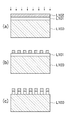
上記梯子状電極304aは、例えばフォトエッチング法により形成することができる。このフォトエッチング方法においては、収差が小さいレンズを用いて原画が1段または2段縮小され、それによりフォトマスクが形成される。このフォトマスクは、ポジまたはネガタイプのレジストが塗布された基板表面に対して、密着または数μmのギャップを設けた状態で保持される。そして、このフォトマスクを用いて高圧水銀灯などの光源により基板表面が露光され、フォトマスクに対応する電極パターンが基板表面に形成される。
The
具体的には、ネガタイプのレジストが用いられる場合、図5(a)に示すように、圧電部材L100上にアルミニウムなどの金属L101が蒸着され、この金属L101上にスピンコーターによりレジストL102が塗布される。次いで、フォトマスク(図示せず)を用いて露光、現像が行われる。これにより、図5(b)に示すように、レジストL102において、電極パターンが形成される。この段階においては、電極を形成する部位のレジストが残存し、その他の部位のレジストはない。次いで、図5(c)に示すように、レジストが残っていない部分(電極を形成しない部位)の金属(アルミニウム)が、NaOHあるいはリン酸系のエッチング液により、除去される。そして、圧電部材L100上に残存する金属部分のレジストがレジスト除去液により、取り除かれる。このような工程を経ることによって、最終的に、梯子状電極304aが形成される。
Specifically, when a negative type resist is used, as shown in FIG. 5A, a metal L101 such as aluminum is vapor-deposited on the piezoelectric member L100, and a resist L102 is applied onto the metal L101 by a spin coater. The Next, exposure and development are performed using a photomask (not shown). Thereby, as shown in FIG.5 (b), an electrode pattern is formed in the resist L102. At this stage, the resist in the part for forming the electrode remains, and there is no resist in the other part. Next, as shown in FIG. 5C, the metal (aluminum) in the portion where the resist is not left (the portion where the electrode is not formed) is removed with NaOH or a phosphoric acid-based etching solution. Then, the resist of the metal portion remaining on the piezoelectric member L100 is removed by the resist removing liquid. Through these steps, a
単相電極トランスデューサ304に対する交流電圧307の印加は、図6に示すように、予め定められた時間に亘り、時間Bが経過する毎に繰り返し行われる。すなわち、交流電圧307の印加は、予め定められた時間中、周期的に繰り返し行われる。ここで、1回当たりの交流電圧307の印加時間は、時間Aに設定されている。本実施の形態においては、時間Aが20μsecに設定され、時間Bが200μsecに設定されている。そして、上記交流電圧307の印加を周期的に繰り返し行う予め定められた時間としては、例えば15秒以上に設定されている。また、圧電部材302などの発熱を抑制するために、時間Aを短くし、時間Bを長くするように設定すればよい。
Application of the
ここで、除去可能な塵埃の大きさは、少なくとも伝播波長V/f以上の大きさである。よって、交流電圧の周波数fを高くするほど、除去可能な塵埃の大きさを小さくすることができる。これに対し、交流電圧のVp−pを一定にした状態において、交流電圧の周波数fを高くするほど、励振される表面弾性波の振幅は、漸次小さくなる。すなわち、表面弾性波の振幅が圧電部材の表面粗さ程度の振幅に達する程度に交流電圧の周波数fを高くすると、逆に、塵埃の除去は困難になり、除去率は低下する。 Here, the size of the dust that can be removed is at least the propagation wavelength V / f or more. Therefore, the higher the frequency f of the AC voltage, the smaller the size of dust that can be removed. On the other hand, in a state where the AC voltage Vp-p is constant, the amplitude of the surface acoustic wave to be excited gradually decreases as the frequency f of the AC voltage is increased. That is, if the frequency f of the AC voltage is increased to such an extent that the amplitude of the surface acoustic wave reaches the amplitude of the surface roughness of the piezoelectric member, it is difficult to remove dust and the removal rate decreases.
よって、上述した交流電圧の周期的な印加方法は、周波数fが高い交流電圧を用いる場合に、交流電圧のVp−pをさらに高くすることを容易にし、より小さな塵埃の除去に大きな効力を発揮する。 Therefore, the periodic application method of the AC voltage described above makes it easy to further increase the AC voltage Vp-p when using an AC voltage having a high frequency f, and exhibits a great effect in removing smaller dust. To do.
上記単相電極トランスデューサ304(電極304a,304b間)に上記交流電圧307が印加されると、図7に示すように、圧電部材302の表面(光入射面)のみに表面弾性波308が励振され、表面弾性波308の伝播部位が楕円運動する。ここで、圧電部材302の表面には、この表面に付着した塵埃311の重力による自重、および静電気力などによる予圧309が働いている。このとき、表面弾性波308の伝播部位の楕円運動と上記予圧309により、付着している塵埃311には、摩擦力310が働き、これにより、付着している塵埃311は、図中の矢印312が示す方向(電極304へ向う方向)へ移動する。そして、上記交流電圧307が予め定められた期間(例えば15秒以上の期間)に亘り印加されると、圧電部材302の表面上にある塵埃311が、取り除かれることになる。
When the
また、交流電圧の周波数fが数MHz以上あるので、耳障りな騒音が発生することはなく、優れた静音性が得られる。 In addition, since the frequency f of the AC voltage is several MHz or more, no harsh noise is generated, and excellent silence is obtained.
次に、上記光学フィルタ301による塵埃の除去効果を確認するための実験方法およびその結果について説明する。ここでは、光学フィルタ301の光入射面(圧電部材302の表面)に付着する塵埃としては、例えば一眼レフレックス方式のデジタルカメラにおいて、レンズ交換時などに外部から侵入するものが想定されている。また、シャッタの動作に伴い当該シャッタの構成部材から生じる磨耗紛などの塵埃が想定されている。本実験においては、上記想定された塵埃に相当する塵埃として、エポキシ系、PC系、ABS系、ポリスチレン系などの樹脂類、フッ素ゴムおよびアルミニウムなどから構成され、塵埃の一粒の大きさが100μm程度に揃えられているものが用いられる。ここで、上記塵埃を構成する成分は、すべて同じ比率で配合されたものである。
Next, an experimental method for confirming the dust removal effect by the
本実験においては、まず、上記塵埃が、圧電部材302の有効領域306にふりかけられる。この塵埃をふりかける操作は、有効領域306における塵埃の付着密度が略均一になるように行われ、その結果は、顕微鏡により観察される。ここでは、最終的に、塵埃の付着密度が、約1000粒/mm2であることが確認されている。そして、圧電部材30
2の表面に表面弾性波308を励振させるために、上記単相電極トランスデューサ304に対して交流電圧307が、上述したように予め定められた期間に亘り周期的に繰り返し印加される。その後、有効領域306上の塵埃の除去状態が、顕微鏡を用いて観察される。その結果、有効領域306から全ての塵埃が取り除かれたことを確認することができた。
In this experiment, first, the dust is sprinkled on the
In order to excite the surface
本実施の形態においては、上記第2の実施の形態において述べたと同様に、フィルタ本体303のみに光学フィルタの機能を持たせるように構成することも可能である。この場合、圧電部材302として、複屈折性を示さないが、可視光領域において光透過性を有する圧電部材例えばZnOなどが使用される。
In the present embodiment, as described in the second embodiment, only the filter
(第4の実施の形態)
次に、本発明の第4の実施の形態について図8を参照しながら説明する。図8は本発明の第4の実施の形態に係る光学フィルタの構成を示す斜視図である。
(Fourth embodiment)
Next, a fourth embodiment of the present invention will be described with reference to FIG. FIG. 8 is a perspective view showing a configuration of an optical filter according to the fourth embodiment of the present invention.
本実施の形態の光学フィルタは、図8に示すように、すだれ状電極トランスデューサ404が形成されている光学フィルタ401である。この光学フィルタ401は、具体的には、光透過性および複屈折性を有するフィルタ本体403を備える。フィルタ本体403の一方の面(光入射面)には、矩形平板状の圧電部材402が接着剤により接合されている。この接着剤としては、例えば屈折率が1.5であるアクリル系またはエポキシ系の接着剤が用いられる。圧電部材402は、大きな電気機械結合係数を有するとともに、透過性および複屈折性を有する。圧電部材402には、有効領域406が規定されている。圧電部材402には、すだれ状電極トランスデューサ404が形成されている。このすだれ状電極トランスデューサ404は、圧電部材402の一方の面(光入射面)に互いに対向するように形成された1対のすだれ状電極404aを含む。各すだれ状電極404aは、有効領域406と干渉しないように配置されている。各すだれ状電極404aは、例えば上記第3の形態において述べたフォトエッチング方法などにより形成される。
As shown in FIG. 8, the optical filter of the present embodiment is an
各すだれ状電極404a間には、交流電圧405が印加される。これにより、圧電部材402の一方の面(光入射面)には、表面弾性波407が励振される。
An
本実施の形態においては、圧電部材402として、厚さ0.4mmのLiNbO3が用いられている。また、フィルタ本体403としては、厚さ2.54mmの水晶が用いられている。この構成の場合、常光線と異常光線との分離幅として、約15μmが得られている。
In the present embodiment,
また、圧電部材402における表面弾性波の伝播速度Vが4000m/sec、交流電圧405の周波数fが50MHzであるとして、すだれ状電極404aの電極間のピッチPが、上記(1)式に基づいて80μmに設定されている。そして、すだれ状電極404aの電極間のピッチPが80μmである場合において、表面弾性波407が最も強く励振されたことが確認されている。
Further, assuming that the propagation velocity V of the surface acoustic wave in the
また、圧電部材402の厚さをtとすると、t>V/fの関係式を満足するように圧電部材402を形成することが好ましい。表面弾性波407のエネルギーのうち、90%以上のエネルギーが、圧電部材402の表面から圧電部材402を伝播する波長λ(=V/f)分の深さ以内に、集中するので、1波長分以上の深さにおいては、生じる振動は僅少となる。換言すれば、圧電部材402の厚さtが、t>V/f(さらに好ましくは、t>2V/f(=二波長分))の関係を満足すれば、フィルタ本体403と圧電部材402との境界部分においては、振動はほとんど発生しない。これにより、圧電部材402が、それに励起される振動により、フィルタ本体402から剥がれる恐れはなく、光学フィルタ401全体の機械的強度を維持することができる。
In addition, when the thickness of the
(第5の実施の形態)
次に、本発明の第5の実施の形態について図9および図10を参照しながら説明する。図9は本発明の第5の実施の形態に係る光学フィルタの構成を示す斜視図である。図10は図9のグループ形一方向性すだれ状電極トランスデューサ504の詳細を示す平面図である。
(Fifth embodiment)
Next, a fifth embodiment of the present invention will be described with reference to FIGS. FIG. 9 is a perspective view showing a configuration of an optical filter according to the fifth embodiment of the present invention. FIG. 10 is a plan view showing details of the group-type unidirectional
上記第4の実施の形態の光学フィルタに採用されているすだれ状電極トランスデューサ(図8)の場合、表面弾性波が、電極の両側の領域において、互いに対向する方向(図8中の表面弾性波の伝播方向とその反対方向)へそれぞれ励振される。従って、交流電圧により投入された電力は、両方向に伝播する表面弾性波に二分され、投入電力のすべてが塵埃除去のために使用されないことになる。すなわち、塵埃の除去効率が悪い。 In the interdigital transducer (FIG. 8) employed in the optical filter of the fourth embodiment, the surface acoustic waves are opposed to each other in the regions on both sides of the electrode (surface acoustic waves in FIG. 8). Direction of propagation and the opposite direction). Therefore, the electric power input by the AC voltage is divided into two by surface acoustic waves propagating in both directions, and all the input electric power is not used for dust removal. That is, dust removal efficiency is poor.
そこで、本実施の形態においては、一方向性すだれ状電極トランスデューサが用いられている。この一方向性すだれ状電極トランスデューサは、塵埃の除去効率を向上させ、消費電力を少なくするという利点を有する。この一方向性すだれ状電極トランスデューサにより、表面弾性波を撮像領域のみにおいて励振することができ、理論的には、投入された電力のすべてが塵埃除去のために使用されることになる。すなわち、本実施の形態の光学フィルタは、上記第4の実施の形態の光学フィルタに比して、より少ない電力で塵埃を除去することができるという効果を奏する。 Therefore, in this embodiment, a unidirectional interdigital transducer is used. This unidirectional interdigital transducer has the advantages of improving dust removal efficiency and reducing power consumption. With this unidirectional interdigital transducer, surface acoustic waves can be excited only in the imaging region, and theoretically, all of the input power is used for dust removal. That is, the optical filter of the present embodiment has an effect that dust can be removed with less electric power than the optical filter of the fourth embodiment.
ここで、一方向性すだれ状電極トランスデューサとしては、単相形一方向性のもの、多相形一方向性のものがあるが、投入電力に対して塵埃除去に費やされる電力の割合をより大きくするためには、多相形一方向性のものを用いることが好ましい。さらに、多相形一方向性すだれ状電極トランスデューサとしては、三相形一方向性のもの、グループ形一方向性のものがあるが、このグループ形一方向性のものを用いることがより好ましい。 Here, as the unidirectional interdigital transducer, there are single-phase unidirectional and multi-phase unidirectional, but in order to increase the ratio of power consumed for dust removal to the input power. It is preferable to use a multiphase unidirectional one. Further, as the multiphase unidirectional interdigital transducer, there are a three-phase unidirectional and a group-type unidirectional, and it is more preferable to use this group-type unidirectional.
本実施の形態の光学フィルタ501においては、図9に示すように、上記第4の実施の形態のすだれ状電極トランスデューサに代えて、グループ形一方向性すだれ状電極トランスデューサ504が形成されている。ここで、圧電部材502、フィルタ本体503は、上記第4の実施の形態における圧電部材402、フィルタ本体403と同等のものであり、その説明は省略する。
In the
グループ形一方向性すだれ状電極トランスデューサ504は、有効領域506と干渉しないように圧電部材502の表面上に形成されている。グループ形一方向性すだれ状電極トランスデューサ504は、互いに対向するように配置されている一対の電極(すだれ状電極)504aと、アース電極504bとを含む。電極504aの一方には、交流電圧505が印加される。電極504aの他方には、交流電圧505がπ/2(rad)の位相器508を介して印加される。すなわち、電極504aの他方には、位相がπ/2(rad)ずれた交流電圧が印加されることになる。
The group-type unidirectional
各電極504aにおいては、図10に示すように、電極間のピッチPが、表面弾性波の波長λ(=V/f)となるように設定されている。また、アース電極504bは、λ/2の電極幅を有し、対となる各電極504aからなるグループ間で励振された表面弾性波が同位相となるように配置されている。本実施の形態においては、圧電部材502の表面弾性波の伝播速度Vが4000m/sであり、交流電圧505の周波数fが50MHzであるので、各電極504aにおける電極間のピッチPは、80μm(λ=V/f)に設定されている。また、アース電極504bの電極幅(λ/2)は、40μmに設定されている。
In each
このグループ形一方向性すだれ状電極トランスデューサ504においては、各電極504aに対して、位相が異なる交流電圧505が印加されるので、圧電部材502の表面上には、一方向性の表面弾性波が励振される。ここで、交流電圧505の印加は、上述したように、予め定められた時間に亘り、周期的に繰り返し行われる。
In this group-type unidirectional
このグループ形一方向性すだれ状電極トランスデューサ504においては、各電極504aのピッチPが80μmで、アース電極504bの電極幅が40μmであるときに、表面弾性波507が最も強く励振されたことが確認されている。また、このときの振動振幅は、約28nmであり、これは、上記第4の実施の形態において同じ交流電圧が印加された場合の約2倍である。
In this group-type unidirectional
(第6の実施の形態)
次に、本発明の第6の実施の形態について図11を参照しながら説明する。図11は上記第5の実施の形態の光学フィルタを搭載する一眼レフレックス方式のデジタルカメラの構成を模式的に示す縦断面図である。
(Sixth embodiment)
Next, a sixth embodiment of the present invention will be described with reference to FIG. FIG. 11 is a longitudinal sectional view schematically showing the configuration of a single-lens reflex digital camera equipped with the optical filter of the fifth embodiment.
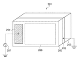
本実施の形態においては、上記第5の実施の形態の光学フィルタを、一眼レフレックス方式のデジタルカメラの光学フィルタに適用した場合を説明する。 In the present embodiment, a case will be described in which the optical filter of the fifth embodiment is applied to an optical filter of a single-lens reflex digital camera.
一眼レフレックス方式のデジタルカメラは、図11に示すように、レンズ装置102を取り外し可能に装着するカメラ本体100を備える。ここで、レンズ装置102には、撮影光の光路L1を規定する撮影光学系103と、撮影光学系103へ光路L1に沿って入射する光量を規制するための絞り104と、端子102aとが組み込まれている。この端子102aは、レンズ装置102がカメラ本体100のマウント機構101と係合されるときに、このマウント機構101に設けられている端子101aと電気的に接続される。これにより、レンズ装置102とカメラ本体100とは電気的に接続され、カメラ本体100は、レンズ装置102の焦点距離、絞り104の設定値など、レンズ装置102が保持する情報を取得することが可能になる。
As shown in FIG. 11, the single-lens reflex digital camera includes a
カメラ本体100は、上記マウント機構101および予め定められた範囲内で可動するハーフミラー111を有する。ハーフミラー111は、上記撮影光学系103から上記光路L1に沿って入射した撮影光のうち、一部をフォーカシングスクリーン105へ向けて反射し、残りを透過する。このハーフミラー111の屈折率は、約1.5であり、その厚さは0.5mmである。ハーフミラー111は、第1の光路分割位置と第2の光路分割位置との間で移動する。ここで、第1の光路分割位置とは、ハーフミラー111が光の一部をフォーカシングスクリーン105へ導く(反射する)位置である。第2の光路分割位置とは、撮光学系103からの光を直接、固体撮像装置15へ導くために、ハーフミラー111が光路L1から退避した位置である(図11中の破線で示した位置111’)。
The
フォーカシングスクリーン105上には、ハーフミラー111により反射された光が結像され、この光像は、ペンタプリズム112内部を経てファインダレンズ109から外部へ導かれる。これにより、撮影者は、ファインダレンズ109を介して、フォーカシングスクリーン105上に結像された光像を観察することができる。上記フォーカシングスクリーン105上には、情報表示ユニット142により、特定の情報(例えばシャッタ速度、絞り値、撮影モードなど)が表示される。
On the focusing
このハーフミラー111の背後には、可動型のサブミラー122が設けられている。このサブミラー122は、ハーフミラー111を透過した光のうち、光路L1に近い光を反射し、この反射光は、焦点検出ユニット121へ導かれる。この焦点検出ユニット121は、サブミラー122からの反射光を受光し、この受光した光に基づいて位相差検出方式による焦点検出を行う。
A
上記サブミラー122は、ハーフミラー111の保持部材(図示せず)に設けられた回転軸(図示せず)を中心に角度的に回転しながら、ハーフミラー111の動きに連動して移動する。ここで、ハーフミラー111が第1の光路分割位置にあるとき、サブミラー122は、ハーフミラー111を透過した光を焦点検出ユニット121へ向けて反射する位置にある。これに対し、ハーフミラー111が第2の光路分割位置へ移動すると、これに連動して、サブミラー122は、光路L1から退避した位置へ移動する(図11中の破線で示した位置122’)。
The
上記ハーフミラー111の背面側には、固体撮像装置15の固体撮像素子15bへ入射する光量を調節するためのフォーカルプレンシャッタ50、光学フィルタ11、固体撮像装置15などが順に配置されている。これらの詳細については、後述する。
On the back side of the
また、カメラ本体100には、可動式閃光発光ユニット114、表示部107、メインスイッチ119、レリーズボタン120、スイッチ123が設けられている。
In addition, the
閃光発光ユニット114は、カメラ本体100に収納される収納位置とカメラ本体100から外部へ露出する発光位置との間で移動可能である。表示部107は、液晶ディスプレイなどから構成され、撮影画像、または撮影モードおよび撮影条件などを含む各種情報を表示する。
The flash
メインスイッチ119は、カメラ本体100を起動させるためのスイッチである。レリーズボタン120は、2段階で押圧操作可能なボタンである。このレリーズボタン120が半押し操作(SW1がオン)されると、撮影準備動作(測光動作や焦点調節動作等)が開始される。また、レリーズボタン120が全押し操作(SW2がオン)されると、撮影動作(固体撮像素子15bから読み出された画像データのメモリへの記録)が開始される。スイッチ123は、カメラ本体100に設定されているモードをクリーニングモードに切り替えるためのモード切り換えスイッチである。このクリーニングモードは、カメラ本体100の光学フィルタ11の表面に付着した異物(塵、埃などの塵埃)を除去するためのモードであり、その詳細については後述する。
The
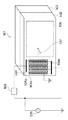
次に、フォーカルプレンシャッタ50および固体撮像装置15周りの構成について図12を参照しながら説明する。図12は図11のフォーカルプレンシャッタ50および固体撮像装置15周りの構成を示す縦断面図である。
Next, the configuration around the
フォーカルプレンシャッタ50は、図12に示すように、先膜21と、後幕22と、押え板24と、カバー板25と、中間板23とを有する。先幕21は、複数のシャッタ羽根21a〜21dから構成される。後幕22は、複数のシャッタ羽根から構成される。押え板24は、後幕22の押え板であり、その中央部には、撮像光を受け入れるための開口24aが設けられている。カバー板25は、先幕21の押え板であり、その中央部には、撮像光を受け入れるための開口25aが設けられている。中間板23は、押え板24とカバー板25との間に挿入されている。この中間板23により、押え板24とカバー板25との間の空間は、先幕21の駆動スペースと後幕22の駆動スペースのそれぞれに分離されている。
As shown in FIG. 12, the
フォーカルプレンシャッタ50の背面側に配置されている光学フィルタ11は、上記第5の実施の形態の光学フィルタ501に相当する構成からなる。ここで、光学フィルタ11は、撮影光学系103からの光のうち、予め定められた帯域の光の通過を制限するような特性を有するように構成されている。光学フィルタ11の縁部は、保持部材12に保持され、保持部材12は、光学フィルタ11と一体化されて支持部材13に支持されている。支持部材13は、カメラ本体100のシャーシ(図示せず)に固定されている。
The
光学フィルタ11の背面側に配置されている固体撮像装置15は、光学フィルタ11側に向けて開口する基体15aを有する。基体15a内には、固体撮像素子15bが組み込まれている。固体撮像素子15bは、例えば増幅型固体撮像素子の1つであるCMOSプロセスコンパチブルのセンサからなる。この固体撮像素子15bには、複数の接続端子15cと接続され、固体撮像素子15bは、各接続端子15cを介して、基板17と電気的に接続される。基体15aの開口部は、固体撮像素子15bを保護するための透明のカバー部材15dにより覆われ、このカバー部材15dにより、基体15a内の空間は、外部と封止されている。
The solid-
このカバー部材15dと光学フィルタ11との間には、間隔が開けられており、カバー部材15dと光学フィルタ11間に生じる空間は、シール部材16により、外部と封止されている。これにより、カバー部材15dと光学フィルタ11間の空間へ塵埃が侵入することが防止されている。基板17および固体撮像装置15は一体化されて保持板18に保持され、保持板18は、カメラ本体100のシャーシ(図示せず)にビス(図示せず)により固定されている。
A space is provided between the
次に、本実施の形態のデジタルカメラの制御構成について図13を参照しながら説明する。図13は図11のデジタルカメラの制御構成を示すブロック図である。 Next, the control configuration of the digital camera of the present embodiment will be described with reference to FIG. FIG. 13 is a block diagram showing a control configuration of the digital camera of FIG.
本実施の形態における制御構成は、図13に示すように、カメラ本体100に設けられているカメラシステム制御部135を有する。カメラシステム制御部135は、CPU600、ROM601およびRAM602を有する。CPU600は、ROM601に格納されているプログラムに従って、カメラ全体の制御を行うとともに、各種の個別制御を行う。RAM602は、CPU600の作業領域を提供する。
As shown in FIG. 13, the control configuration in the present embodiment includes a camera
カメラシステム制御部135は、レンズ装置102がマウント機構101を介してカメラ本体100と装着されると、端子101aと端子102aとが電気的に接続される。これにより、カメラシステム制御部135は、レンズシステム制御部141と通信可能になる。レンズシステム制御部141は、レンズ装置102の状態(絞り104の絞り値、焦点距離、フォーカスレンズ位置など)を示すレンズ状態信号を、カメラシステム制御部135へ送出する。
When the
カメラシステム制御部135には、上記レンズ状態信号、操作検出部136からの検出信号、AF制御部140からの信号などが入力される。ここで、操作検出部136は、メインスイッチ119、レリーズボタン120、スイッチ123などの操作の有無を検出し、その検出結果を示す操作検出信号をカメラシステム制御部135へ出力する。AF制御部140は、スイッチ焦点検出ユニット121からの出力信号に基づいて撮影光学系103の焦点調節状態(デフォーカス量)を示す信号を生成し、カメラシステム制御部135へ出力する。焦点検出ユニット121は、撮影画面内の予め定められた位置に設けられた焦点検出領域内における像の合焦状態を検出し、この検出結果を示す信号を出力する。
The camera
カメラシステム制御部135は、上記レンズ状態信号、操作検出部136からの検出信号、AF制御部140からの信号などに基づいて、レンズシステム制御部141およびカメラ本体100の各部のそれぞれに対して個別に制御信号を生成する。この制御信号は、動作タイミング、動作内容などを制御するための信号である。
The camera
ここで、カメラ本体100には、ハーフミラー駆動部138、シャッタ制御部145、光学フィルタ駆動部139、基板17が設けられており、それぞれに対する制御信号がカメラシステム制御部135により個別に生成される。また、A/D変換器130、RGB画像処理部131、YC処理部132、記録処理部133、再生処理部133、情報表示部142などが設けられており、それぞれに対する制御信号がカメラシステム制御部135により個別に生成される。
Here, the
レンズシステム制御部141は、カメラシステム制御部135からの制御信号に基づいて、絞り104を駆動する絞り駆動部143の駆動信号を生成する。絞り駆動部143は、上記駆動信号により、絞り104の絞り口径が上記制御信号により指示された絞り値になるように、絞り104を駆動する。また、レンズシステム制御部141は、カメラシステム制御部135からの制御信号に基づいて、撮影光学系103のフォーカスレンズを駆動するAFモータ147の駆動信号を生成する。この駆動信号により、AFモータ147は、上記フォーカスレンズを上記制御信号により指示された位置へ移動させる。
The lens
カメラ本体100のハーフミラー駆動部138は、カメラシステム制御部135からの制御信号に基づいて、ハーフミラー111を駆動する。シャッタ制御部145は、カメラシステム制御部135からの制御信号に基づいてフォーカルプレンシャッタ50を駆動する。光学フィルタ駆動部139は、カメラシステム制御部135からの制御信号に基づいて、光学フィルタ11のグループ形一方向性すだれ状電極トランスデューサ(図8の504)に対して予め定められた周波数の交流電圧を予め定められた期間に亘り周期的に繰り返し印加する。これにより、光学フィルタ11の表面(光入射面)には、表面弾性波が励振される。基板17は、カメラシステム制御部135からの制御信号に基づいて、予め定められたタイミングで、固体撮像装置15の撮像信号(電気信号)を読み出し、この読み出された撮像信号を、A/D変換器130へ出力する。
The half
A/D変換器130は、上記撮像信号の振幅に応じて、当該撮像信号を例えば10ビットのR,G,Bの各デジタル信号に変換する。RGB画像処理部131は、A/D変換器130から入力されたR,G,Bの各デジタル信号に対して、ホワイトバランス、ガンマ補正、補間演算による高解像度化処理などを施す。YC処理部132は、RGB画像処理部131から入力されたR,G,Bの各デジタル信号から、輝度信号Yおよび色差信号R−Y,B−Yを生成する。この生成された輝度信号Yおよび色差信号R−Y,B−Yは、画像信号として、記録処理部133へ入力される。A/D変換器130、RGB画像処理部131、YC処理部132のそれぞれの動作は、カメラシステム制御部135からそれぞれに対して出力される制御信号により制御される。
The A /
記録処理部133は、カメラシステム制御部135からの制御信号に基づいて、入力された画像信号を例えばCFカード(登録商標)などのメモリ(図示せず)への書き込み処理、またメモリからの画像信号の読み出し処理を行う。再生処理部134は、カメラシステム制御部135からの制御信号に基づいて、上記メモリから読み出された画像信号を再生し、表示部107に出力する。この再生処理部134および表示部107を、 Bluetooth(登録商標)などの無線通信を介して接続するような構成を採用することも可能である。この場合、このカメラで撮像された画像をカメラから離れた位置でモニタすることができる。
Based on the control signal from the camera
情報表示ユニット142は、カメラシステム制御部135からの制御信号に基づいて、フォーカシングスクリーン105上に特定の情報を表示する。この表示する特定の情報は、カメラシステム制御部135から、上記制御信号とともに与えられる情報である。閃光発光ユニット114は、カメラシステム制御部135からの制御信号に基づいて、予め定められたタイミングで閃光を発光する。
The
次に、本実施の形態におけるクリーニングモードについて図14を参照しながら説明する。図14はカメラシステム制御部135によるクリーニングモードを実施するための手順を示すフローチャートである。この手順は、カメラシステム制御部135のROM601に記憶されているプログラムに従ってCPU600により実行される。
Next, the cleaning mode in the present embodiment will be described with reference to FIG. FIG. 14 is a flowchart showing a procedure for performing the cleaning mode by the camera
クリーニングモードは、上述したように、カメラ本体100の光学フィルタ11の表面に付着した塵埃を除去するためのモードである。このクリーニングモードは、スイッチ123の切り換え操作に応答して、実施されることになる。
The cleaning mode is a mode for removing dust adhering to the surface of the
カメラシステム制御部135のCPU600は、図16に示すように、操作検出部136からの信号に基づいて、スイッチ123の操作によるクリーニングモードへの切り換えが行われたか否かを監視している(ステップS100)。ここで、クリーニングモードへの切り換えが行われたことが検出されると、CPU600は、クリーニングモードへの切り換え直前に設定されていたモードおよび撮影条件(シャッタ速度、絞り値など)をRAM602に記憶する(ステップS101)。そして、CPU600は、光学フィルタ駆動部139に対して、交流電圧の印加を指示するための制御信号を出力する(ステップS102)。光学フィルタ駆動部139は、上記制御信号に基づいて、光学フィルタ11のグループ形一方向性すだれ状電極トランスデューサに対して予め定められた周波数の交流電圧の印加を開始する。
As shown in FIG. 16, the
次いで、CPU600は、タイマ(図示せず)に予め定められた時間をセットし、タイマによる予め定められた時間の計時を開始する(ステップS103)。そして、CPU600は、このタイマによる予め定められた時間の計時終了を待つ(ステップS104)。この予め定められた時間中、交流電圧は、光学フィルタ11のグループ形一方向性すだれ状電極トランスデューサに対して予め定められた期間に亘り周期的に繰り返し印加され、光学フィルタ11の表面には、表面弾性波が励振される。本実施の形態においては、予め定められた時間として例えば20秒が設定されている。そして、上記表面弾性波により、光学フィルタ11の表面に付着した塵埃は、当該表面上から離脱し、カメラ本体100の下部へ向けて落下する。
Next,
そして、上記タイマによる予め定められた時間の計時が終了すると、CPU600は、光学フィルタ駆動部139に対して、交流電圧の印加停止を指示するための制御信号を出力する(ステップS105)。光学フィルタ駆動部139は、上記制御信号に基づいて、光学フィルタ11上の電極への交流電圧の印加を停止する。これにより、光学フィルタ11の表面上における表面弾性波の励振は停止され、クリーニングモードが終了する。
When the predetermined time measurement by the timer ends, the
次いで、CPU600は、クリーニングモードが終了した旨のメッセージを表示部107に表示する(ステップS106)。そして、CPU600は、上記ステップS101においてRAM602に記憶したモードおよび撮影条件などを読み出し、この読み出されたモードおよび撮影条件に対応する状態への復帰を行う(ステップS107)。そして、CPU600は、本処理を終了する。
Next, the
このように本実施の形態によれば、上記第5の実施の形態の光学フィルタ(501)を光学フィルタ11として用いることによって、固体撮像装置15とシャッタ50間の距離を、従来の塵埃除去機構を用いた場合に比して大幅に低減することができる。すなわち、シャッタ効率を低下させることなく、撮像された画像に写り込む影の要因となる塵埃を除去することができる。
As described above, according to the present embodiment, by using the optical filter (501) of the fifth embodiment as the
また、光学フィルタ11の表面に表面弾性波を励振させることにより、光学フィルタ11の表面上の塵埃を容易に除去することができる。すなわち、レンズ交換などの際に侵入する塵埃またはシャッタ50の駆動時に生じる磨耗紛などが光学フィルタ11の表面上に付着したとしても、その塵埃を除去することが可能である。その結果、常に良好な画質による撮影を行うことができる一眼レフレックス方式のデジタルカメラを提供することができる。
Moreover, dust on the surface of the
本実施の形態においては、上記第5の実施の形態の光学フィルタ(501)の構成に相当する構成を有する光学フィルタ11として用いている。これに代えて、上記第1〜第4の実施の形態の光学フィルタのいずれかに相当する構成を有する光学フィルタ11を用いることも可能である。そして、この場合も、同様の効果を得ることができる。
In the present embodiment, it is used as the
本実施の形態においては、スイッチ123の操作に応じて、クリーニングモードの実施が制御されるが、これに代えて、電源投入をトリガーとしてクリーニングモードを実施するようなシーケンスを採用することも可能である。また、撮影動作が終了すると、これをトリガーとしてクリーニングモードを実施するようなシーケンスを採用することも可能である。
In the present embodiment, the execution of the cleaning mode is controlled in accordance with the operation of the
1,1’,11,201,301,401,501 光学フィルタ
2,203,303,403,503 フィルタ本体
3,3a,3b,204,205,304a,304b,404a,404b,504a,504b 電極
5,206,307,405,505 交流電圧
304 単相電極トランスデューサ
404 すだれ状電極トランスデューサ
504 グループ形一方向性すだれ状電極トランスデューサ
1, 1 ', 11, 201, 301, 401, 501
Claims (3)
透過性を有し、前記フィルタ本体の光入射面上に重ね合わせて接合されている圧電部材と、
前記圧電部材に形成され、駆動電圧の印加により前記圧電部材の光入射面上に表面弾性波を励振させるすだれ状電極トランスデューサと、
前記すだれ状電極トランスデューサに駆動電圧を印加する駆動電圧印加手段を備え、
前記すだれ状電極トランスデューサは、互いに対向するように配置される一対のすだれ状電極と、アース電極とを含み、
前記アース電極は前記表面弾性波の波長の1/2の電極幅を有し、対となる前記すだれ状電極の間に配置され、
前記駆動電圧印加手段によって前記一対のすだれ状電極の一方に印加される駆動電圧と前記一対のすだれ状電極の他方に印加される駆動電圧とは位相がπ/2(rad)ずれていることを特徴とする光学装置。 A filter body having a preset transmission characteristic;
A piezoelectric member having transparency and bonded to the light incident surface of the filter body in an overlapping manner;
An interdigital transducer that is formed on the piezoelectric member and excites a surface acoustic wave on the light incident surface of the piezoelectric member by applying a driving voltage;
Drive voltage application means for applying a drive voltage to the interdigital transducer,
The interdigital transducer includes a pair of interdigital electrodes arranged to face each other, and a ground electrode,
The ground electrode has an electrode width of ½ of the wavelength of the surface acoustic wave, and is disposed between the pair of interdigital electrodes,
The drive voltage applied to one of the pair of interdigital electrodes by the drive voltage applying means and the drive voltage applied to the other of the pair of interdigital electrodes are shifted in phase by π / 2 (rad). Optical device characterized.
Priority Applications (2)
| Application Number | Priority Date | Filing Date | Title |
|---|---|---|---|
| JP2006108860A JP5268232B2 (en) | 2006-04-11 | 2006-04-11 | Optical device |
| US11/733,313 US7787031B2 (en) | 2006-04-11 | 2007-04-10 | Image-pickup apparatus for dust prevention |
Applications Claiming Priority (1)
| Application Number | Priority Date | Filing Date | Title |
|---|---|---|---|
| JP2006108860A JP5268232B2 (en) | 2006-04-11 | 2006-04-11 | Optical device |
Publications (3)
| Publication Number | Publication Date |
|---|---|
| JP2007279592A JP2007279592A (en) | 2007-10-25 |
| JP2007279592A5 JP2007279592A5 (en) | 2009-05-21 |
| JP5268232B2 true JP5268232B2 (en) | 2013-08-21 |
Family
ID=38681078
Family Applications (1)
| Application Number | Title | Priority Date | Filing Date |
|---|---|---|---|
| JP2006108860A Expired - Fee Related JP5268232B2 (en) | 2006-04-11 | 2006-04-11 | Optical device |
Country Status (1)
| Country | Link |
|---|---|
| JP (1) | JP5268232B2 (en) |
Families Citing this family (5)
| Publication number | Priority date | Publication date | Assignee | Title |
|---|---|---|---|---|
| JP5109412B2 (en) * | 2007-03-02 | 2012-12-26 | セイコーエプソン株式会社 | Dust-proof substrate and electro-optical device using the same |
| JP5094628B2 (en) * | 2008-08-08 | 2012-12-12 | キヤノン株式会社 | Imaging apparatus and control method thereof |
| JP5402130B2 (en) * | 2009-03-19 | 2014-01-29 | 株式会社ニコン | Optical apparatus and imaging apparatus |
| JP6380385B2 (en) * | 2013-05-22 | 2018-08-29 | リコーイメージング株式会社 | Imaging apparatus and control method thereof |
| CN107911594B (en) * | 2017-12-19 | 2019-09-13 | Oppo广东移动通信有限公司 | Bracket component and its manufacturing method, camera and electronic equipment |
Family Cites Families (3)
| Publication number | Priority date | Publication date | Assignee | Title |
|---|---|---|---|---|
| JP2001359287A (en) * | 2000-06-12 | 2001-12-26 | Minolta Co Ltd | Surface acoustic wave optical element |
| JP4282226B2 (en) * | 2000-12-28 | 2009-06-17 | オリンパス株式会社 | camera |
| JP2005072778A (en) * | 2003-08-21 | 2005-03-17 | Canon Inc | Optical equipment |
-
2006
- 2006-04-11 JP JP2006108860A patent/JP5268232B2/en not_active Expired - Fee Related
Also Published As
| Publication number | Publication date |
|---|---|
| JP2007279592A (en) | 2007-10-25 |
Similar Documents
| Publication | Publication Date | Title |
|---|---|---|
| JP5003216B2 (en) | Imaging device and optical device | |
| JP5004677B2 (en) | Optical device | |
| JP5110971B2 (en) | Optical device | |
| CN101770144B (en) | Vibrating device and image equipment having the same | |
| CN101770143B (en) | Vibrating device and image equipment having the same | |
| JP2007129642A (en) | Imaging device | |
| US7787031B2 (en) | Image-pickup apparatus for dust prevention | |
| JP4891154B2 (en) | Optical device | |
| JP4804251B2 (en) | Imaging device and imaging unit | |
| JP5268232B2 (en) | Optical device | |
| JP4719705B2 (en) | Imaging device and imaging unit | |
| JP4759462B2 (en) | Imaging device and imaging unit | |
| JP2008028669A (en) | Imaging apparatus | |
| JP4859212B2 (en) | Imaging device | |
| JP4921060B2 (en) | Imaging device and imaging unit | |
| JP5264302B2 (en) | Imaging device | |
| JP5762034B2 (en) | Foreign object removal unit and optical apparatus provided with the same | |
| JP5159198B2 (en) | Imaging device | |
| JP2009159268A (en) | Optical apparatus | |
| JP4788384B2 (en) | Imaging device | |
| JP5283837B2 (en) | Optical equipment | |
| JP4926586B2 (en) | Imaging device and imaging unit | |
| JP5228507B2 (en) | Optical component, imaging device and optical apparatus | |
| JP5268236B2 (en) | Imaging device and imaging unit | |
| JP2008026530A (en) | Imaging apparatus |
Legal Events
| Date | Code | Title | Description |
|---|---|---|---|
| A521 | Request for written amendment filed |
Free format text: JAPANESE INTERMEDIATE CODE: A523 Effective date: 20090402 |
|
| A621 | Written request for application examination |
Free format text: JAPANESE INTERMEDIATE CODE: A621 Effective date: 20090402 |
|
| A977 | Report on retrieval |
Free format text: JAPANESE INTERMEDIATE CODE: A971007 Effective date: 20120209 |
|
| A131 | Notification of reasons for refusal |
Free format text: JAPANESE INTERMEDIATE CODE: A131 Effective date: 20120221 |
|
| A521 | Request for written amendment filed |
Free format text: JAPANESE INTERMEDIATE CODE: A523 Effective date: 20120420 |
|
| A131 | Notification of reasons for refusal |
Free format text: JAPANESE INTERMEDIATE CODE: A131 Effective date: 20121120 |
|
| A521 | Request for written amendment filed |
Free format text: JAPANESE INTERMEDIATE CODE: A523 Effective date: 20130118 |
|
| A131 | Notification of reasons for refusal |
Free format text: JAPANESE INTERMEDIATE CODE: A131 Effective date: 20130212 |
|
| A521 | Request for written amendment filed |
Free format text: JAPANESE INTERMEDIATE CODE: A523 Effective date: 20130411 |
|
| TRDD | Decision of grant or rejection written | ||
| A01 | Written decision to grant a patent or to grant a registration (utility model) |
Free format text: JAPANESE INTERMEDIATE CODE: A01 Effective date: 20130430 |
|
| A61 | First payment of annual fees (during grant procedure) |
Free format text: JAPANESE INTERMEDIATE CODE: A61 Effective date: 20130507 |
|
| LAPS | Cancellation because of no payment of annual fees |