JP5247556B2 - Optical device - Google Patents
Optical device Download PDFInfo
- Publication number
- JP5247556B2 JP5247556B2 JP2009074859A JP2009074859A JP5247556B2 JP 5247556 B2 JP5247556 B2 JP 5247556B2 JP 2009074859 A JP2009074859 A JP 2009074859A JP 2009074859 A JP2009074859 A JP 2009074859A JP 5247556 B2 JP5247556 B2 JP 5247556B2
- Authority
- JP
- Japan
- Prior art keywords
- vibration
- vibration detection
- detection electrode
- pass filter
- optical low
- Prior art date
- Legal status (The legal status is an assumption and is not a legal conclusion. Google has not performed a legal analysis and makes no representation as to the accuracy of the status listed.)
- Expired - Fee Related
Links
Images


Classifications
-
- G—PHYSICS
- G03—PHOTOGRAPHY; CINEMATOGRAPHY; ANALOGOUS TECHNIQUES USING WAVES OTHER THAN OPTICAL WAVES; ELECTROGRAPHY; HOLOGRAPHY
- G03B—APPARATUS OR ARRANGEMENTS FOR TAKING PHOTOGRAPHS OR FOR PROJECTING OR VIEWING THEM; APPARATUS OR ARRANGEMENTS EMPLOYING ANALOGOUS TECHNIQUES USING WAVES OTHER THAN OPTICAL WAVES; ACCESSORIES THEREFOR
- G03B17/00—Details of cameras or camera bodies; Accessories therefor
- G03B17/28—Locating light-sensitive material within camera
-
- G—PHYSICS
- G03—PHOTOGRAPHY; CINEMATOGRAPHY; ANALOGOUS TECHNIQUES USING WAVES OTHER THAN OPTICAL WAVES; ELECTROGRAPHY; HOLOGRAPHY
- G03B—APPARATUS OR ARRANGEMENTS FOR TAKING PHOTOGRAPHS OR FOR PROJECTING OR VIEWING THEM; APPARATUS OR ARRANGEMENTS EMPLOYING ANALOGOUS TECHNIQUES USING WAVES OTHER THAN OPTICAL WAVES; ACCESSORIES THEREFOR
- G03B17/00—Details of cameras or camera bodies; Accessories therefor
- G03B17/02—Bodies
-
- H—ELECTRICITY
- H04—ELECTRIC COMMUNICATION TECHNIQUE
- H04N—PICTORIAL COMMUNICATION, e.g. TELEVISION
- H04N23/00—Cameras or camera modules comprising electronic image sensors; Control thereof
- H04N23/50—Constructional details
- H04N23/54—Mounting of pick-up tubes, electronic image sensors, deviation or focusing coils
-
- H—ELECTRICITY
- H04—ELECTRIC COMMUNICATION TECHNIQUE
- H04N—PICTORIAL COMMUNICATION, e.g. TELEVISION
- H04N23/00—Cameras or camera modules comprising electronic image sensors; Control thereof
- H04N23/80—Camera processing pipelines; Components thereof
- H04N23/81—Camera processing pipelines; Components thereof for suppressing or minimising disturbance in the image signal generation
- H04N23/811—Camera processing pipelines; Components thereof for suppressing or minimising disturbance in the image signal generation by dust removal, e.g. from surfaces of the image sensor or processing of the image signal output by the electronic image sensor
Landscapes
- Engineering & Computer Science (AREA)
- Multimedia (AREA)
- Signal Processing (AREA)
- Physics & Mathematics (AREA)
- General Physics & Mathematics (AREA)
- Studio Devices (AREA)
- Camera Bodies And Camera Details Or Accessories (AREA)
Description
本発明は、撮像装置等の光学装置において、光軸上に配設された光学部材を振動させて、その表面に付着した塵埃等の異物を除去する技術に関する。 The present invention relates to a technique for removing foreign matters such as dust attached to the surface of an optical device such as an imaging device by vibrating an optical member disposed on an optical axis.
被写体像を電気信号に変換して撮像するデジタルカメラ等の撮像装置では、撮影光束を撮像素子で受光し、その撮像素子から出力される光電変換信号を画像データに変換して、メモリカード等の記録媒体に記録する。撮像素子としては、CCD(Charge Coupled Device)やCMOSセンサ(Complementary Metal Oxide Semiconductor)等が用いられる。 In an imaging device such as a digital camera that captures a subject image by converting it into an electrical signal, the imaging light beam is received by the imaging device, a photoelectric conversion signal output from the imaging device is converted into image data, and a memory card, etc. Record on a recording medium. A CCD (Charge Coupled Device), a CMOS sensor (Complementary Metal Oxide Semiconductor), or the like is used as the imaging element.
このような撮像装置では、撮像素子の被写体側に、光学ローパスフィルタや赤外吸収フィルタが配置されるが、これらフィルタの表面に塵埃等の異物が付着すると、その付着部分が黒い点となって撮影画像に写り込み、画像の見栄えが低下してしまう。 In such an image pickup apparatus, an optical low-pass filter and an infrared absorption filter are arranged on the subject side of the image pickup element. When foreign matter such as dust adheres to the surface of these filters, the attached portion becomes a black dot. The image appears in the photographed image, and the image looks poor.
特にレンズ交換可能なデジタル一眼レフカメラでは、シャッタやクイックリターンミラーといった機械的な作動部が撮像素子の近傍に配置されており、それらの作動部から発生した塵埃等の異物が撮像素子やフィルタの表面に付着することがある。また、レンズ交換時に、レンズマウントの開口から塵埃等の異物がカメラ本体内に入り込み、これが付着することもある。 Especially in digital SLR cameras with interchangeable lenses, mechanical operation parts such as shutters and quick return mirrors are arranged in the vicinity of the image sensor, and foreign matters such as dust generated from these operation parts are captured by the image sensor and filter. May adhere to the surface. In addition, when the lens is replaced, foreign matter such as dust may enter the camera body from the opening of the lens mount and adhere to it.
このような現象を回避するために、特許文献1には、撮像素子の被写体側に撮影光束を透過させる防塵フィルタを設け、これを圧電素子で振動させることにより、防塵フィルタの表面に付着した塵埃等の異物を除去する技術が提案されている。
In order to avoid such a phenomenon, in
この際、塵埃等の異物を効率よく除去するためには、圧電素子により防塵フィルタを共振周波数で振動させて、振動の振幅を大きくさせることが望ましい。しかし、共振周波数は防塵フィルタの外形、板厚、物性値等により決定されるため、加工精度や製造工程等のバラツキ発生要因により、各々の防塵フィルタごとに共振周波数は異なる。 At this time, in order to efficiently remove foreign matters such as dust, it is desirable to vibrate the dustproof filter at the resonance frequency by the piezoelectric element to increase the amplitude of the vibration. However, since the resonance frequency is determined by the outer shape, plate thickness, physical property value, and the like of the dustproof filter, the resonance frequency differs for each dustproof filter due to factors such as processing accuracy and manufacturing process variations.
そこで、特許文献1に開示されたカメラにおいては、円形の防塵フィルタ(防塵用光学部材)の周縁部に振動を与えるための圧電素子を配置し、光学部材の振動状態を検出するために、圧電素子上に駆動用とは別に検出用の電極を1つ設ける。そして、その電極電圧をモニタしながら共振周波数を探し出し、その共振周波数を用いて光学部材を振動させ、光学部材の表面に付着した塵埃等を除去するようにしている。
Therefore, in the camera disclosed in
一般的に、防塵フィルタを振動させる周波数を変化させると、様々な振動モードが現れる。そして、各々の振動モードに応じて、振動の節の発生位置は異なる。節は振幅がゼロの箇所であるので、節の発生位置によっては、防塵フィルタの異物除去能力を阻害してしまう。ゆえに、狙いの振動モードの近傍の周波数において、除去能力を阻害してしまう振動モードが発生することがしばしば起こりうる。特に、円形よりも矩形の防塵フィルタを振動させる場合、その現象が顕著である。よって、狙いの振動モードを発生させる周波数を正確に探し出すことが重要である。さらに具体的に言うと、狙いの位置に節が発生する周波数を探し出すことが重要である。 Generally, various vibration modes appear when the frequency for vibrating the dustproof filter is changed. And the generation | occurrence | production position of the vibration node differs according to each vibration mode. Since the node is a portion where the amplitude is zero, the foreign matter removing ability of the dustproof filter is hindered depending on the position where the node is generated. Therefore, it is often possible that a vibration mode that inhibits the removal capability occurs at a frequency in the vicinity of the target vibration mode. In particular, when a dustproof filter having a rectangular shape rather than a circular shape is vibrated, the phenomenon is remarkable. Therefore, it is important to accurately find the frequency that generates the target vibration mode. More specifically, it is important to find the frequency at which the node occurs at the target position.
しかしながら、上述した振動検出用の電極を1つ設ける構成では、狙いの位置に節が発生する周波数であるか否かを判断することは困難である。つまり、狙いの振動モードを発生させる周波数を正確に把握することは困難である。 However, in the above-described configuration in which one electrode for vibration detection is provided, it is difficult to determine whether or not the frequency is a frequency at which a node is generated at the target position. That is, it is difficult to accurately grasp the frequency that generates the target vibration mode.
本発明は以上のような状況に鑑みてなされたものであり、圧電部材により被振動部材を振動させる際に、狙いの位置に節を発生させる周波数を正確に検出できるようにすることを目的とする。 The present invention has been made in view of the above situation, and it is an object of the present invention to accurately detect a frequency at which a node is generated at a target position when a vibrating member is vibrated by a piezoelectric member. To do.
本発明の光学装置は、被振動部材と、第一面に設けられた駆動電極、前記第一面に前記駆動電極とは独立して設けられた第一の振動検出電極及び第二の振動検出電極、及び前記第一面の裏面である第二面に設けられたグランド電極を有し、前記被振動部材の表面に付着した異物を除去するために前記被振動部材を振動させる圧電部材と、前記駆動電極に接続され、前記圧電部材を駆動する駆動手段と、前記第一の振動検出電極及び前記第二の振動検出電極から出力される信号に基づいて前記被振動部材の振動状態を検出する振動検出手段と、前記振動検出手段により検出された結果に基づいて前記被振動部材が所定の振動モードで振動しているか否かを判定する判定手段とを備え、前記第一の振動検出電極及び前記第二の振動検出電極は同一形状であり、かつ、前記所定の振動モードにおいて発生する所定の振動の節を軸として対称となるように、前記第一面に配置されていることを特徴とする。 The optical device of the present invention, and the object to be vibration member, a driving electrode provided on the first surface, the first vibration detection electrode and the second vibration detection electrodes provided independently of the driving electrode on the first surface , and have a ground electrode provided on the second surface is a rear surface of the first surface, and a piezoelectric member that Ru is vibrated the object to be vibration member for removing foreign matters adhering to the surface of the object to be vibration member, Based on signals output from the drive means connected to the drive electrode and driving the piezoelectric member, and from the first vibration detection electrode and the second vibration detection electrode, the vibration state of the member to be vibrated is detected. Vibration detection means, and determination means for determining whether or not the member to be vibrated in a predetermined vibration mode based on a result detected by the vibration detection means, the first vibration detection electrode and The second vibration detection electrode is the same It is Jo, and the section of a predetermined vibration generated in the predetermined vibration mode so as to be symmetrical as an axis, characterized in that it is disposed on the first surface.
本発明によれば、圧電部材により被振動部材を振動させる際に、狙いの振動モードを発生させる、つまり狙いの位置に節を発生させる周波数を正確に検出することができる。これにより、被振動部材の表面に付着した塵埃等の異物の除去を効果的に行うことが可能になる。 According to the present invention, it is possible to accurately detect a frequency at which a target vibration mode is generated, that is, a node is generated at a target position, when the vibrating member is vibrated by the piezoelectric member. This makes it possible to effectively remove foreign matters such as dust attached to the surface of the vibration member.
以下、添付図面を参照して、本発明の好適な実施の形態について説明する。
<カメラの構成>
図1は、本実施の形態に係る光学装置としての撮像装置、具体的にはデジタル一眼レフカメラの主要部の電気的構成を示すブロック図である。図1において、カメラ本体に内蔵されたマイクロコンピュータからなる中央処理装置(以下、「MPU」という。)100は、カメラの動作制御を司るものであり、各要素に対して様々な処理や指示を実行する。
DESCRIPTION OF EXEMPLARY EMBODIMENTS Hereinafter, preferred embodiments of the invention will be described with reference to the accompanying drawings.
<Camera configuration>
FIG. 1 is a block diagram illustrating an electrical configuration of a main part of an imaging apparatus as an optical apparatus according to the present embodiment, specifically, a digital single lens reflex camera. In FIG. 1, a central processing unit (hereinafter referred to as “MPU”) 100 comprising a microcomputer built in the camera body controls the operation of the camera, and performs various processes and instructions on each element. Run.
MPU100には、ミラー駆動回路101、焦点検出回路102、シャッタ駆動回路103、映像信号処理回路104、スイッチセンサ回路105、測光回路106が接続されている。また、LCD駆動回路107、バッテリチェック回路108、時刻計測回路109、電力供給回路110、圧電素子駆動回路111、振動検出回路112が接続されている。これらの回路は、MPU100の制御により動作するものである。
Connected to the
MPU100は、撮影レンズユニット200a内のレンズ制御回路201とマウント接点21を介して通信を行う。マウント接点21は、撮影レンズユニット200aが接続されるとMPU100へ信号を送信する機能も有する。これにより、レンズ制御回路201は、MPU100との間で通信を行い、AF駆動回路202及び絞り駆動回路203を介して撮影レンズユニット200a内の撮影レンズ200及び絞り204の駆動を行う。なお、図1では便宜上1枚の撮影レンズ200のみを図示しているが、実際は多数のレンズ群によって構成される。
The MPU 100 communicates with the
AF駆動回路202は、例えばステッピングモータによって構成され、レンズ制御回路201の制御により撮影レンズ200内のフォーカスレンズ位置を変化させ、撮像素子33に撮影光束の焦点を合わせるように調整する。絞り駆動回路203は、例えばオートアイリス等によって構成され、レンズ制御回路201の制御により絞り204を変化させ、光学的な絞り値を得る。
The
メインミラー6は、図1に示す撮影光軸に対して45°の角度に保持された状態で、撮影レンズ200を通過する撮影光束をペンタダハミラー22へ導くと共に、その一部を透過させてサブミラー30へ導く。サブミラー30は、メインミラー6を透過した撮影光束を焦点検出センサユニット31へ導く。
The
ミラー駆動回路101は、例えばDCモータとギヤトレイン等によって構成され、メインミラー6を、ファインダにより被写体像を観察可能とする位置と、撮影光束から待避する位置とに駆動する。メインミラー6が駆動すると、同時にサブミラー30も、焦点検出センサユニット31へ撮影光束を導く位置と、撮影光束から待避する位置とに移動する。
The
焦点検出センサユニット31は、不図示の結像面近傍に配置されたフィールドレンズ、反射ミラー、2次結像レンズ、絞り、複数のCCDからなるラインセンサ等によって構成され、位相差方式の焦点検出を行う。焦点検出センサユニット31から出力される信号は、焦点検出回路102へ供給され、被写体像信号に換算された後、MPU100に送信される。MPU100は、被写体像信号に基づいて位相差検出法による焦点検出演算を行う。そして、デフォーカス量及びデフォーカス方向を求め、これに基づいて、レンズ制御回路201及びAF駆動回路202を介して撮影レンズ200内のフォーカスレンズを合焦位置まで駆動する。
The focus
ペンタダハミラー22は、メインミラー6により反射された撮影光束を正立正像に変換反射する。撮影者はファインダ光学系を介してファインダ接眼窓18から被写体像を観察することができる。ペンタダハミラー22は、撮影光束の一部を測光センサ23へも導く。測光回路106は、測光センサ23の出力を得て、観察面上の各エリアの輝度信号に変換し、MPU100に出力する。MPU100は、輝度信号に基づいて露出値を算出する。
The
シャッタユニット(機械フォーカルプレーンシャッタ)32は、撮影者がファインダにより被写体像を観察している時には、シャッタ先幕が遮光位置にあると共に、シャッタ後幕が露光位置にある。次いで、撮影時には、シャッタ先幕が遮光位置から露光位置へ移動する露光走行を行って被写体からの光を通過させ、撮像素子33で撮像を行う。所望のシャッタ秒時の経過後、シャッタ後幕が露光位置から遮光位置へ移動する遮光走行を行って撮影を完了する。機械フォーカルプレーンシャッタ32は、MPU100の指令を受けたシャッタ駆動回路103により制御される。
The shutter unit (mechanical focal plane shutter) 32 has a shutter front curtain in a light shielding position and a shutter rear curtain in an exposure position when a photographer observes a subject image with a finder. Next, at the time of shooting, the shutter front curtain travels from the light shielding position to the exposure position, passes light from the subject, and the
撮像ユニット400は、光学ローパスフィルタ410、圧電素子430、撮像素子33が後述する他の部品と共にユニット化されたものである。撮像素子33は、被写体の光学像を光電変換して電気信号にするものであり、本実施の形態ではCMOSセンサが用いられるが、その他にもCCD型、CMOS型及びCID型等様々な形態があり、いずれの形態の撮像デバイスを採用してもよい。撮像素子33の前方に配置された光学ローパスフィルタ410は、水晶からなる1枚の複屈折板であり、その形状は矩形状である。圧電素子430は、単板の圧電素子(ピエゾ素子)であり、MPU100の指示を受けた圧電素子駆動回路111により加振され、その振動を光学ローパスフィルタ410に伝えるように構成されている。
In the
クランプ/CDS(相関二重サンプリング)回路34は、A/D変換する前の基本的なアナログ処理を行うものであり、クランプレベルを変更することも可能である。AGC(自動利得調整装置)35は、A/D変換する前の基本的なアナログ処理を行うものであり、AGC基本レベルを変更することも可能である。A/D変換器36は、撮像素子33のアナログ出力信号をデジタル信号に変換する。
The clamp / CDS (correlated double sampling) circuit 34 performs basic analog processing before A / D conversion, and the clamp level can be changed. The AGC (automatic gain adjusting device) 35 performs basic analog processing before A / D conversion, and can change the AGC basic level. The A /
映像信号処理回路104は、デジタル化された画像データに対してガンマ/ニー処理、フィルタ処理、モニタ表示用の情報合成処理等、ハードウエアによる画像処理全般を実行する。この映像信号処理回路104からのモニタ表示用の画像データは、カラー液晶駆動回路113を介してカラー液晶モニタ19に表示される。また、映像信号処理回路104は、MPU100の指示に従って、メモリコントローラ38を通じてバッファメモリ37に画像データを保存することもできる。さらに、映像信号処理回路104は、JPEG等の画像データ圧縮処理を行うこともできる。連写撮影等、連続して撮影が行われる場合は、一旦バッファメモリ37に画像データを格納し、メモリコントローラ38を通して未処理の画像データを順次読み出すこともできる。これにより、映像信号処理回路104は、A/D変換器36から入力されてくる画像データの速度に関わらず、画像処理や圧縮処理を順次行うことができる。
The video
メモリコントローラ38は、外部インタフェース40から入力される画像データをメモリ39に記憶し、メモリ39に記憶されている画像データを外部インタフェース40から出力する機能を有する。メモリ39としては、カメラ本体に着脱可能なフラッシュメモリ等が用いられる。
The
スイッチセンサ回路105は、各スイッチの操作状態に応じて入力信号をMPU100に送信する。スイッチSW1(7a)は、レリーズボタンの第1ストローク(半押し)によりONする。スイッチSW2(7b)は、レリーズボタンの第2ストローク(全押し)によりONする。スイッチSW2(7b)がONされると、撮影開始の指示がMPU100に送信される。また、スイッチセンサ回路105には、メイン操作ダイヤル8、サブ操作ダイヤル20、撮影モード設定ダイヤル14、メインスイッチ43、クリーニング指示操作部材44が接続されている。クリーニング指示操作部材44は、光学ローパスフィルタ410の表面に付着した塵埃等の異物を手動で除去するための動作を指示するためのものである。
The
LCD駆動回路107は、MPU100の指示に従って、LCD表示パネル9やファインダ内液晶表示装置41を駆動する。
The
バッテリチェック回路108は、MPU100の指示に従って、バッテリチェックを行い、その検出結果をMPU100に送信する。電源42は、カメラの各要素に対して電源を供給する。
The
時刻計測回路109は、メインスイッチ43がOFFされて次にONされるまでの時間や日付を計測し、MPU100からの指示に従って、計測結果をMPU100に送信する。
The
<異物除去構造>
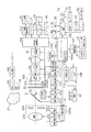
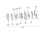
次に、本実施の形態における光学ローパスフィルタ410を加振する異物除去構造について説明する。図2は、本実施の形態に係る撮像ユニット400まわり保持構造を示すためのカメラ内部の概略構成を示す分解斜視図である。図3は、図2における撮像ユニット400の構成を概略的に示す分解斜視図である。
<Foreign matter removal structure>
Next, a foreign matter removing structure for exciting the optical low-
図2において、カメラ本体の骨格となる本体シャーシ300の被写体側には、被写体側から順に、ミラーボックス5、シャッタユニット32が配設される。また、本体シャーシ300の撮影者側には、撮像ユニット400が配設される。撮像ユニット400は、撮影レンズユニット200aが取り付けられる基準となるマウント部2の取付面に撮像素子33の撮像面が所定の距離を空けて且つ平行になるように調整されて固定される。
In FIG. 2, the
図3において、光学ローパスフィルタ410は、水晶からなる1枚の複屈折板であり、その形状は矩形状である。この光学ローパスフィルタ410が本発明でいう板状の矩形部材をなす被振動部材であり、撮像素子33の前方に光軸上に配設された光学部材に相当するものである。光学ローパスフィルタ410は、撮影有効領域外の両側に一対の圧電素子430a及び430bを配置し、撮影光軸中心に対して直交する方向(カメラ左右方向)は対称である。このようにした光学ローパスフィルタ410の表面には、光学的なコーティングが施されている。
In FIG. 3, an optical low-
圧電素子430a及び430bは、電圧の印加により光軸と直交する方向に主として伸縮振動し、光学ローパスフィルタ410を振動させる。圧電素子430a及び430bは、光学ローパスフィルタ410の向かい合う二辺近傍にそれぞれ接着される(貼着される)。より詳しくは、圧電素子430a及び430bは、単板の矩形の短冊形状を呈し、光学ローパスフィルタ410の周縁部において、圧電素子430a及び430bの長辺が光学ローパスフィルタ410の短辺(側辺)に平行になるように配置されて接着保持される。すなわち、圧電素子430a及び430bは、光学ローパスフィルタ410のカメラ左右方向の辺の付近に平行に貼着され、辺に平行な複数の節部を有するように光学ローパスフィルタ410を波状に振動させる。この圧電素子430a及び430bが本発明でいう圧電部材に相当するものである。
The
光学ローパスフィルタ保持部材420は、樹脂製又は金属製であり、光学ローパスフィルタ410を保持し、撮像素子保持部材510にビス固定される。
The optical low-pass
付勢部材440は、光学ローパスフィルタ410及び不図示の遮光マスクを撮像素子33の方向に付勢し、光学ローパスフィルタ保持部材420に係止される。付勢部材440は、カメラ本体のグランドに接地され、光学ローパスフィルタ410の表面(光学的なコーティングが施された面)もカメラ本体のグランドに接地される。これにより、光学ローパスフィルタ410の表面への塵埃等の静電気的な付着を抑制することができる。
The urging
弾性部材450は、断面が略円形の枠状を呈し、光学ローパスフィルタ410と光学ローパスフィルタ保持部材420とで挟まれて密着保持される。この密着力は、付勢部材440の撮像素子33方向への付勢力により決定される。なお、弾性部材450はゴムでもよいし、弾性体であれば、ポロンやプラスチック等の高分子重合体を用いてもよい。
The
光学部材460は、位相板(偏光解消板)と赤外カットフィルタと光学ローパスフィルタ410に対して屈折方向が90°異なる複屈折板とを貼り合わせた光学部材であり、光学ローパスフィルタ保持部材420に接着固定される。
The
撮像素子保持部材510は、矩形の開口部を有する板状を呈し、その開口部に撮像素子33を露出させるように撮像素子33が固着する。撮像素子保持部材510の周囲には、ミラーボックス5に3ヵ所でビス固定するための腕部が設けられている。
The imaging
マスク520は、撮像素子33に撮影光路外からの余計な光が入射することを防ぐためのものであり、光学ローパスフィルタ保持部材420と撮像素子33とで挟まれて密着保持される。
The
左右一対の撮像素子付勢部材530は、板バネ状であり、撮像素子保持部材510にビス固定され、撮像素子33を撮像素子保持部材510に押し付ける。
The pair of left and right image
以上の構成をとることにより、光学ローパスフィルタ410は、付勢部材440と弾性部材450とで挟み込まれて振動自在に支持される。
By adopting the above configuration, the optical low-
<圧電素子の電極配置>
図4は、図3における圧電素子430a及び430bの詳細を説明するための図である。図4に示すように、圧電素子430上には電極が配置されている。圧電素子430のB面(本発明でいう第一面)は、光学ローパスフィルタ410に振動を励起するための+相と、振動検出のためのSa相及びSb相と、G相とに分割されている。これらの+相、Sa相、Sb相、G相が、それぞれ本発明でいう駆動電極、第一の振動検出電極、第二の振動検出電極、グランド電極に相当するものである。また、圧電素子430のC面(本発明でいう第一面の裏面である第二面)は、不図示の導電材等により電気的に接続されてB面のG相と同電位に保たれている。
<Electrode arrangement of piezoelectric element>
FIG. 4 is a diagram for explaining the details of the
B面には不図示の圧電素子用フレキシブルプリント基板が接着等により固着され、それぞれの電極に接続される。+相は制御回路である圧電素子駆動回路111が接続され、回路から周期的な電圧が印加されることにより圧電素子430は伸縮運動する。また、G相はグランドに接続される。また、Sa相、Sb相はそれぞれ独立して振動検出回路112に接続される。圧電素子駆動回路111が本発明でいう駆動手段、振動検出回路112が本発明でいう振動検出手段に相当するものである。
A flexible printed circuit board for piezoelectric elements (not shown) is fixed to the B surface by adhesion or the like, and is connected to each electrode. The + phase is connected to a piezoelectric
Sa相及びSb相は振動検出相であり、圧電素子430が伸縮することにより発生する分極電荷(圧電効果)を取り出すための相である。このSa相及びSb相は同一形状であり、詳しくは後述するが、光学ローパスフィルタ410を狙いの振動モードで振動させた際に発生する振動の節を軸として対称に配置されている。
The Sa phase and the Sb phase are vibration detection phases, and are phases for taking out polarization charges (piezoelectric effect) generated by the expansion and contraction of the
このように電極配置された圧電素子430のC面が光学ローパスフィルタ410に接着等により固着され、圧電素子430と光学ローパスフィルタ410とが一体的に運動するように構成されている。よって、圧電素子430に周期的な電圧を印加することで、光学ローパスフィルタ410を振動させることができる。
The C surface of the
<振動の説明>
次に、図5〜図12を用いて、本実施の形態における光学ローパスフィルタ410の振動の説明を行う。本実施の形態では、塵埃等の異物を搬送することのできる振動を光学ローパスフィルタ410に発生させ、異物を除去している。具体的に言うと、光学ローパスフィルタ410に接着された圧電素子430a及び430bを、次数の1つ異なる二つの曲げ振動を、時間位相をずらして励起することによって異物の搬送を行っている。なお、搬送動作の原理の説明に目的を絞るため、必要最小限の構成である、光学ローパスフィルタ410、圧電素子430a及び430bの構成で説明を行う。
<Description of vibration>
Next, the vibration of the optical low-
図5は、本実施の形態における光学ローパスフィルタ410に励起される2つの振動モードの周波数と振幅の関係を示すグラフである。図5に示すように、f(m)で示される周波数でm次の振動モードが励起され、f(m+1)で示される周波数でm+1次の振動モードが励起される。ここで、圧電素子430a及び430bに印加する電圧の周波数fをf(m)<f<f(m+1)に設定すると、m次のモードとm+1次のモード両方の共振を利用することができる。fをf<f(m)に設定すると、m次の共振を利用することはできるが、f(m+1)次の共振点から離れるため、m+1次モードの振幅を大きくすることは困難となる。また、f(m+1)<fとした場合は、m+1次のモードのみ振幅が大きくなってしまう。本実施の形態では、両方の振動モードを利用するため、周波数fはf(m)<f<f(m+1)となる範囲で設定する。
FIG. 5 is a graph showing the relationship between the frequency and amplitude of the two vibration modes excited by the optical low-
図6(A)及び図6(B)は、mが奇数の場合のm次及びm+1次の振動モード形状、並びに圧電素子430a及び430bに印加される電圧を示す図である。また、図7(A)及び図7(B)は、mが偶数の場合のm次及びm+1次の振動モード形状、並びに圧電素子430a及び430bに印加される電圧を示す図である。
FIGS. 6A and 6B are diagrams illustrating m-order and m + 1-order vibration mode shapes when m is an odd number, and voltages applied to the
図6(A)及び図6(B)では、mが奇数のときの例としてm=9の場合を示す。図6(A)に示すように、それぞれのモードで圧電素子430の長手方向に平行な向きに(同一方向に)複数の節が等間隔で現れる。図6(B)には、それぞれのモードで圧電素子430a及び430bに印加される交流電圧の振幅と時間的位相が、実数成分と虚数成分で表されている。(1)はm次の振動モードの、(2)はm+1次の振動モードの、(3)はm+1次の振動モードを90°時間位相をずらしたものの、交流電圧を示している。なお、ここでは、ある周波数の交流電圧に対するm次振動モードとm+1次振動モードの振幅比をA:1として、2つのモードで同じ振幅を出すために、各モードの電圧をm次の振動モードの振幅で規格化している。光学ローパスフィルタ410にm次の振動モードと、時間位相が90°異なるm+1次の振動モードを同時に励起させるためには、(1)と(3)の交流電圧を足せばよい。すなわち、(4)に示すような、交流電圧を印加すればよい。
6A and 6B show a case where m = 9 as an example when m is an odd number. As shown in FIG. 6A, a plurality of nodes appear at equal intervals in the direction parallel to the longitudinal direction of the piezoelectric element 430 (in the same direction) in each mode. In FIG. 6B, the amplitude and temporal phase of the alternating voltage applied to the
同様にして、図7(A)及び図7(B)には、mが偶数のときの例としてm=10の場合において、振動モード形状と、圧電素子430a及び430bに印加される交流電圧とを示す。
Similarly, FIGS. 7A and 7B show the vibration mode shape and the AC voltage applied to the
なお、本実施の形態では、m次とm+1次の振動モードの位相差を90°としたが、交流電圧の振幅、位相、及び周波数を制御することで2つのモードの重ね合わせ方は任意に制御することが可能である。 In this embodiment, the phase difference between the m-th order and m + 1-order vibration modes is set to 90 °. However, by controlling the amplitude, phase, and frequency of the AC voltage, the two modes can be arbitrarily superimposed. It is possible to control.
次に、上記の制御方法によって、2つの振動モードを同時に励起した場合の光学ローパスフィルタ410の挙動について説明する。図8に示すように、光学ローパスフィルタ410に対して、9次と10次の振動モードを同時に励起する場合を考える。図中A,Bで示されているのが、9次、10次の振動モード形状である。光学ローパスフィルタ410の左端から右端までを0〜360の数値で表している。また、図中に示すように、光学ローパスフィルタ410の長辺方向をX、短辺方向をY、面の法線方向をZとする。
Next, the behavior of the optical low-
上記の2つのモードを時間位相を90°ずらして、同時に励起した場合の光学ローパスフィルタ410の各時間位相での挙動を図9〜図12に示す。図9〜図12における各時間位相において、図中Cは9次の振動モード波形、Dは10次の振動モード波形を表している。また、Eが2つのモードが合成された波形、つまり実際の光学ローパスフィルタ410の振幅を表している。Fは光学ローパスフィルタ410のZ方向の加速度である。
FIGS. 9 to 12 show the behavior of the optical low-
光学ローパスフィルタ410の表面に付着した異物は、光学ローパスフィルタ410が変形することによって、法線方向の力を受けて移動して行く。つまり、Z方向の加速度を示す曲線Fが正の値をとるとき、異物は面外に突き上げられ、この時間位相における光学ローパスフィルタ410の変位を示す曲線Eの法線方向の力を受ける。図中rn(n=1、2、3、…)で示した区間では、異物は右方向(X方向の正の向き)に力を受ける。図中ln(n=1、2、3、…)で示した区間では、異物は左方向(X方向負の向き)に力を受ける。結果として、Xn(n=1、2、3、…)で示す場所に異物は移動する。本実施の形態では、このXn(n=1、2、3、…)が時間位相が進むにつれてX方向正の向きに移動して行くことによって、異物がX方向正の向きに移動して行く。
The foreign matter adhering to the surface of the optical low-
本実施の形態では、2つのモードの時間位相差を90°としたが、これに限らず、0°より大きく180°より小さく設定してもよい。この場合でも、上記Xnにあたる箇所がX方向正の向きに移動して行くので、異物をX方向正の向きに搬送することが可能である。また、2つのモードの時間位相差を−180°より大きく0°より小さくする場合は、上記Xnに相当する箇所がX方向負の向きに移動して行くので、上記の例とは反対方向に異物を搬送することが可能である。 In this embodiment, the time phase difference between the two modes is set to 90 °. However, the present invention is not limited to this, and it may be set larger than 0 ° and smaller than 180 °. Even in this case, since the portion corresponding to Xn moves in the positive direction in the X direction, the foreign matter can be conveyed in the positive direction in the X direction. Further, when the time phase difference between the two modes is made larger than −180 ° and smaller than 0 °, the portion corresponding to the above Xn moves in the negative direction of the X direction, so that it is in the opposite direction to the above example. It is possible to transport foreign matter.
また、異物の搬送力は光学ローパスフィルタ410の加速度によって決定される。光学ローパスフィルタ410の加速度aは、駆動周波数をf、振幅をP、駆動電圧をV、k1、k2を比例定数として、以下の式で表される。
a=k1P(2πf)2=k2V(2πf)2
つまり、異物の搬送力は光学ローパスフィルタ410の振幅及び駆動周波数の二乗に比例する。よって、圧電素子430に印加する交流電圧Vと周波数fを上げることで、搬送力を上げることができる。
In addition, the foreign substance conveyance force is determined by the acceleration of the optical low-
a = k 1 P (2πf) 2 = k 2 V (2πf) 2
That is, the foreign substance conveyance force is proportional to the amplitude of the optical low-
<振動状態の検出>
上述したように周波数f(f(m)<f<f(m+1))で光学ローパスフィルタ410を振動させ、異物を搬送させる。このとき、周波数fは、f(m)からf(m+1)の間で、最も搬送に適した振動モードが励起される周波数でなければならない。
<Detection of vibration state>
As described above, the optical low-
図13は光学ローパスフィルタ410の振動モードの概略図であり、図13(A)は周波数fにおける振動モード、図13(B)は周波数fの近傍のある1つの周波数における振動モードを表している。図中の点線は、振動の節を表している。
13A and 13B are schematic diagrams of vibration modes of the optical low-
図13(A)の振動モードが搬送能力を最大限発揮できるモードであり、狙いの振動モード(所定の振動モード)である。このモードでは、縦方向(光学ローパスフィルタ410の短辺に平行な方向、換言すれば、異物の搬送方向に直交する方向)に節が発生する(m次振動モード(図中ではm=10))。それに加え、上下に1つずつ横方向(光学ローパスフィルタ410の長辺に平行な方向、換言すれば、異物の搬送方向に平行な方向)に節が発生する。この横方向の節は、異物の搬送を阻害するものであるが、異物を除去すべき有効光束(撮影エリア)の外部にあるため、有効光束内の異物除去能力は確保される。
The vibration mode in FIG. 13 (A) is a mode in which the conveyance capability can be maximized, and is a target vibration mode (predetermined vibration mode). In this mode, nodes occur in the vertical direction (the direction parallel to the short side of the optical low-
一方、図13(B)は、図13(A)に加えてさらに上下に1つずつ横方向の節が多く発生する振動モードであり、周波数fの近傍に存在するものである。このモードは、有効光束内に異物搬送能力を阻害する横方向の節が存在しており、異物搬送の振動を起こす上で、使用を避けるべきモードである。また、横方向の節が増えるにつれて、縦方向の振幅は小さくなってしまい、その結果さらに搬送能力は落ちることになる。 On the other hand, FIG. 13B is a vibration mode in which a large number of horizontal nodes are generated one above the other in addition to FIG. 13A, and is present in the vicinity of the frequency f. This mode is a mode that should be avoided in order to cause vibration of foreign matter conveyance because there is a lateral node that hinders the foreign matter conveyance ability in the effective light beam. In addition, as the number of nodes in the horizontal direction increases, the amplitude in the vertical direction decreases, and as a result, the conveyance capacity further decreases.
本説明では一例として、図13(B)に示す振動モードを取り上げたが、周波数fの近傍には他にも様々な振動モードが存在し、その多くが横方向の節を数多く含むものである。そのような振動モードを使用すると、搬送能力は大きく損なわれてしまう。よって、振動モードが図13(A)に示すようになる、言い換えると、横方向の節の発生箇所が有効光束の外部で上下に1つずつとなる周波数fを正確に検出し、その周波数fを使用することが異物を搬送させる振動を発生させる上で非常に重要になってくる。 In this description, the vibration mode shown in FIG. 13B is taken as an example, but there are various other vibration modes in the vicinity of the frequency f, and many of them include a large number of nodes in the horizontal direction. When such a vibration mode is used, the conveyance capability is greatly impaired. Therefore, the vibration mode is as shown in FIG. 13A, in other words, the frequency f at which the horizontal node is generated one by one above and below the effective light flux is accurately detected, and the frequency f It is very important to generate vibrations that convey foreign substances.
以下では、図14及び図15を参照して、周波数fの検出方法について説明する。図14は、周波数fにおける振動モードを光学ローパスフィルタ410、圧電素子430a及び430bの構成で表している。図中の点線は、振動の節を表している。縦方向の節はm次(図中ではm=10)、横方向の節は1次の振動モードである。図14に示すように、横方向の節は光学ローパスフィルタ410の中心軸(異物の搬送方向に平行な中心軸)を対称に上下に1つずつ(上下に一対)発生する。その「下側」の横方向の節を軸として対称に、同一形状の振動検出電極Sa及びSbを圧電素子430a、430b上に配置する。ここで、振動検出電極Sa及びSbの電圧出力は、圧電素子430a、430bのいずれにおいても同じであるので、圧電素子430a、430bのいずれか一方に振動検出電極Sa及びSbを配置しても良い。また、「下側」ではなく、「上側」の横方向の節を軸として対称に振動検出電極Sa及びSbを配置するようにしても良い。
Hereinafter, a method for detecting the frequency f will be described with reference to FIGS. 14 and 15. FIG. 14 shows the vibration mode at the frequency f by the configuration of the optical low-
ここで、振動検出電極Sa及びSbは光学ローパスフィルタ410の中心軸に対して「上側」もしくは「下側」のいずれか一方のみに配置されることが望ましい。なぜなら、横節は中心軸対称であるので「上側」と「下側」の振動検出電極Sa及びSbによる出力波形の関係は同じであり、いずれか一方を見れば十分であるからである。さらに、「上側」と「下側」の両方に振動検出電極を配置してしまうと、駆動相である+相の面積が小さくなり、光学ローパスフィルタ410を振動させる能力そのものが阻害されてしまうからである。
Here, it is desirable that the vibration detection electrodes Sa and Sb are disposed only on either the “upper side” or the “lower side” with respect to the central axis of the optical low-
図15は、上記のように配置された振動検出電極Sa及びSbの出力電圧の波形を表している。圧電素子430の振動に伴って、圧電効果により電極Sa及びSbには正弦波の電圧が発生する。このとき、電極Gは常にグランド(0[V])に保たれており、振動検出回路112により、図15に示される正弦波形が得られる。ここで検出される電位差は、圧電素子430の、ひいては光学ローパスフィルタ410の振動振幅に比例するものである。したがって、出力電圧波形をモニタすることで、圧電素子430の、ひいては光学ローパスフィルタ410の振動状態を検出することが可能となる。
FIG. 15 shows the waveform of the output voltage of the vibration detection electrodes Sa and Sb arranged as described above. Along with the vibration of the
図15(A)に、周波数fにおける振動モード時の出力を示す。振動検出電極Sa及びSbの出力電圧値Vsa及びVsbはいずれも同電圧Vaであり、かつ、逆位相(位相が180°異なる)となる。これは、圧電素子430の伸縮は振動の節を境として180°位相が異なることを利用している。逆に言うと、図15(A)のような出力が得られるということは、振動検出電極Sa及びSbが軸対称形状であるとき、その対称軸上に横節が発生していることを意味している。
FIG. 15A shows the output in the vibration mode at the frequency f. The output voltage values Vsa and Vsb of the vibration detection electrodes Sa and Sb are both the same voltage Va and have opposite phases (the phases differ by 180 °). This utilizes the fact that the expansion and contraction of the
一方、図15(B)及び図15(C)に、周波数fの近傍の周波数における振動モード時の出力を示す。図15(B)は、図13(B)で示すような振動モード時の出力を表している。振動検出電極Sa及びSbの出力電圧値Vsa及びVsbはいずれも同電圧Vbであり、かつ、逆位相(位相が180°異なる)となる。ただし、図15(A)と比較すると、Vb<Vaとなっている。これは、図13(B)のように、振動検出電極Sa及びSbの対称軸上に横節がありつつ、さらにその対称軸上以外の箇所にも横節が発生すると、圧電素子430の伸縮量が小さくなり、その結果出力が小さくなるからである。よって、Vb<Vaとなる。
On the other hand, FIG. 15B and FIG. 15C show outputs in the vibration mode at frequencies near the frequency f. FIG. 15B shows an output in the vibration mode as shown in FIG. The output voltage values Vsa and Vsb of the vibration detection electrodes Sa and Sb are both the same voltage Vb and have opposite phases (the phases differ by 180 °). However, Vb <Va as compared with FIG. As shown in FIG. 13B, when a horizontal node is present on the symmetry axis of the vibration detection electrodes Sa and Sb and a horizontal node is generated at a location other than the symmetry axis, the
また、図15(C)は、振動検出電極Sa及びSbの対称軸上に横節がなく、振動検出電極Sa及びSbが共に横節に対して同一側にある場合の振動モード時の出力を表している。振動検出電極Saの出力電圧値VsaはVca、振動検出電極Sbの出力電圧値VsbはVcbであり、両者の出力電圧波形は同位相となる。 FIG. 15C shows the output in the vibration mode when there is no horizontal node on the symmetry axis of the vibration detection electrodes Sa and Sb, and the vibration detection electrodes Sa and Sb are both on the same side with respect to the horizontal node. Represents. The output voltage value Vsa of the vibration detection electrode Sa is Vca, the output voltage value Vsb of the vibration detection electrode Sb is Vcb, and both output voltage waveforms have the same phase.
以上のことから、ある周波数で圧電素子430を駆動し、図15(A)に示される出力波形とは異なる図15(B)又は図15(C)の出力波形が検出された場合は、その周波数は狙いの位置に節が発生していない、つまり狙いの振動モードではないことが分かる。よって、振動検出電極Sa及びSbの出力電圧波形から異物の搬送能力を最大限発揮できる周波数を正確に特定することができる。
From the above, when the
次に、図16に、搬送振動を発生させる周波数fを決定する動作を示す。ステップS101において、MPU100の指示により周波数fの検出を開始する。ステップS102において、圧電素子駆動回路111によりf(m)<f<f(m+1)において、ある周波数fで圧電素子430を振動させる。ステップS103において、その時の振動検出電極Sa及びSbの出力電圧波形を振動検出回路112にて読み取る。そして、ステップS104において、振動検出電極Sa及びSbの出力電圧値Vsa及びVsbがいずれも同電圧(同じ大きさ)で、かつ、所定値Vconst以上であり、さらに両者が逆位相(位相が180°異なる)であるか否かをMPU100にて判断する。このMPU100が本発明でいう判定手段に相当する。なお、所定値Vconstは、図15(A)の出力Vaに係数をかけて決定される値である。そして、条件を満たさない場合は、狙いの位置に横節が発生していない、つまり狙いの振動モードではないと判断し、周波数fを異なる値に変えて、ステップS102〜ステップS105を繰り返し実行する。つまり、条件を満たすまで、周波数fを漸次変化させながら、ステップS102〜ステップS105を繰り返し実行する。そして、ステップS104において条件を満たすと、ステップS105において周波数fを搬送振動を発生させる周波数fとして決定する。その後、ステップS107に移行し、周波数fの検出を終了する。
Next, FIG. 16 shows an operation for determining the frequency f for generating the carrier vibration. In step S101, the detection of the frequency f is started by an instruction from the
この周波数fの検出動作は、工場での量産工程内で行うことはもとより、ユーザ使用時においても行うことが可能である。これは、カメラの使用環境(例えば使用温度や圧電素子の長時間使用による経時変化)によって、異物の搬送に適した周波数fの値が変化するからである。ユーザが異物除去のためのクリーニング動作を行うたびに、毎回最適な周波数fを決定し、その周波数fを用いることで、その使用環境中で最大の異物搬送能力を発揮することができる。 The detection operation of the frequency f can be performed not only in a mass production process at a factory but also when used by a user. This is because the value of the frequency f suitable for the conveyance of the foreign matter changes depending on the use environment of the camera (for example, change over time due to use temperature or long-time use of the piezoelectric element). Each time the user performs a cleaning operation for removing foreign matter, the optimum frequency f is determined each time, and by using the frequency f, the maximum foreign matter conveying ability can be exhibited in the usage environment.
また、この周波数fの検出動作を、故障検知もしくは異常検知として利用することも可能である。上記の周波数の検出動作時において、検出される振幅が想定される振幅を大幅に下回る場合や、振動検出波形が異常な形を示す場合、この異物除去ユニットが異常であると認識でき、異物除去ユニットの動作停止及び交換等の対処を施すことができる。 Further, the detection operation of the frequency f can be used as failure detection or abnormality detection. If the detected amplitude is significantly lower than the expected amplitude during the above frequency detection operation, or if the vibration detection waveform shows an abnormal shape, this foreign matter removal unit can be recognized as abnormal and the foreign matter removal It is possible to take measures such as stopping and replacing the unit.
<異物除去動作>
次に、図17を参照して、光学ローパスフィルタ410の表面に付着した塵埃等の異物を除去する動作について説明する。ステップS1で、メインスイッチ43により電源がONされたか否かを判定する。電源がONされると、ステップS2で、カメラシステムを起動させるための処理を行い、電力供給回路110を制御して各回路へ電力を供給し、システムを初期設定し、カメラとして撮影動作可能にするためのカメラシステムON動作を行う。
<Foreign matter removal operation>
Next, with reference to FIG. 17, an operation for removing foreign matters such as dust adhering to the surface of the optical low-
次に、ステップS3で、撮影者によりクリーニング指示操作部材44が操作されたか否かを判定し、操作されている場合はステップS4に進み、操作されていない場合はステップS5へ進む。なお、本実施の形態ではクリーニング指示操作部材44を設けたが、本発明はこれに限定されるものではない。例えば、クリーニングモードへの移行を指示するための操作部材は、機械的なボタンに限らず、カラー液晶モニタ19に表示されたメニューから、カーソルキーや指示ボタン等を用いて指示するものであっても良い。
Next, in step S3, it is determined whether or not the cleaning
ステップS4では、クリーニングモード開始の指令を受けて、カメラ本体をクリーニングモードの状態に移行させる。まず電力供給回路110は、クリーニングモードに必要な電力をカメラ本体の各部へ供給する。また、これに並行して電源42の電池残量を検出して、その結果をMPU100へ送信する。MPU100は、クリーニングモード開始の信号を受け取ると、まず搬送振動を発生させる周波数fを検出するモードを実行し、周波数fを決定する(図16を参照)。そして、圧電素子駆動回路111はMPU100より指示を受けて、決定された周波数fの周期電圧を生成し、圧電素子430a及び430bを、次数の1つ異なる二つの曲げ振動を、時間位相をずらして励起させる。これによって光学ローパスフィルタ410に搬送波を発生させ、異物を搬送により除去する。クリーニングモードが終了するとステップS5に進む。
In step S4, in response to the instruction to start the cleaning mode, the camera body is shifted to the cleaning mode. First, the
ステップS5で、スイッチSW1(7a)、スイッチSW2(7b)、メイン操作ダイヤル8、サブ操作ダイヤル20、撮影モード設定ダイヤル14、他のスイッチ等の信号を受け、カメラ動作を行う。カメラ動作は、一般的に知られるカメラの撮影/設定等を行うモードで、ここでは詳細な説明は省略する。
In step S5, signals from the switch SW1 (7a), the switch SW2 (7b), the main operation dial 8, the
次に、ステップS6で、カメラが待機状態においてメインスイッチ43にて電源がOFFされたか否かを判定し、OFFされるとステップS7に進み、OFFされていなければステップS3に戻る。 Next, in step S6, it is determined whether the power is turned off by the main switch 43 when the camera is in a standby state. If turned off, the process proceeds to step S7, and if not turned off, the process returns to step S3.
ステップS7では、ステップS4と同様のクリーニングモードを実行後、ステップS8に進む。ここで、ステップS7におけるクリーニングモードでは、カメラの消費電力、動作時間等を考慮して、圧電素子430の駆動周波数、駆動時間、制御法等のパラメータをステップS4と異ならしめても良いことは言うまでも無い。
In step S7, after executing the same cleaning mode as in step S4, the process proceeds to step S8. Here, in the cleaning mode in step S7, parameters such as the driving frequency, driving time, and control method of the
ステップS8では、MPU100の制御により各回路を終了させるための制御を行い、必要な情報等をEEPROM100aに格納し、電力供給回路110を制御して各回路への電源供給を遮断する電源OFF動作を行う。このように、撮影者が意図した任意のタイミングだけではなく、電源OFFのタイミングでもクリーニングモードが実行される。すなわち、光学ローパスフィルタ410の表面に付着した異物を除去する動作を行ってから、カメラシステムOFF動作を行うようにしている。
In step S8, control for terminating each circuit is performed under the control of the
ここで、光学ローパスフィルタ410の表面に付着した異物には様々なものが存在するが、一般的に異物が付着した状態で長期間放置すると、クリーニングモードで振動をかけても除去しにくいことが実験的に解明した。これは、環境(温度や湿度)の変化で結露することにより液架橋力等の付着力が増大したり、環境の変化で塵埃が膨潤、乾燥を繰り返すことにより粘着したりすることによるものと考えられる。また、ゴム等の弾性材では、自身に含まれる油脂等が時間と共にブリードして粘着する。そのため、電源OFF操作のタイミングでクリーニングモードを実行することが、異物を除去しにくい状態になっている可能性の高い長期間未使用状態後の電源ON操作のタイミングで行うよりも、より効率的・効果的である。
Here, there are various kinds of foreign matters attached to the surface of the optical low-
以上詳述したように、本実施の形態では、光学ローパスフィルタ410を搬送振動させる際、搬送に最も適した狙いの振動モードを発生させる周波数を正確に検出することができる。したがって、その周波数を用いることにより、光学ローパスフィルタ410上の異物を効率よく搬送し、除去することができる。
As described above in detail, in the present embodiment, when the optical low-
なお、本発明でいう光学部材は光学ローパスフィルタ410に限定されるものではない。上述した実施の形態では水晶複屈折板に振動を励起する構成としたが、複屈折板の材質は水晶ではなくニオブ酸リチウムを用いてもよい。また、複屈折板と位相板と赤外吸収フィルタとの貼り合わせによって構成される光学ローパスフィルタや赤外吸収フィルタ単体に振動を励起する構成にしてもよい。また、複屈折板の前に配置したガラス板単体に振動を励起する構成にしてもよい。
The optical member referred to in the present invention is not limited to the optical low-
以上、本発明を実施する場合の好適な実施の形態を説明したが、本発明はこの実施の形態にのみ限定されるものではなく、本発明の趣旨を実現する範囲内で適宜変更可能である。例えば、本実施の形態ではデジタルカメラに本発明を適用した例を説明したが、液晶プロジェクタ等の光学装置にも本発明を適用することが可能である。液晶プロジェクタのような光学装置においても、投影光学系の光学部材の表面に塵埃等の異物が付着した場合、異物の影が投影されてしまうため、本実施の形態と同様の構成を取り得る。 As mentioned above, although preferred embodiment in the case of implementing this invention was described, this invention is not limited only to this embodiment, In the range which implement | achieves the meaning of this invention, it can change suitably. . For example, in this embodiment, an example in which the present invention is applied to a digital camera has been described. However, the present invention can also be applied to an optical apparatus such as a liquid crystal projector. Even in an optical apparatus such as a liquid crystal projector, when a foreign matter such as dust adheres to the surface of the optical member of the projection optical system, a shadow of the foreign matter is projected, and thus the same configuration as in this embodiment can be taken.
100:MPU、111:圧電素子駆動回路、112:振動検出回路、400:撮像ユニット、410:光学ローパスフィルタ、430:圧電素子 100: MPU, 111: Piezoelectric element drive circuit, 112: Vibration detection circuit, 400: Imaging unit, 410: Optical low-pass filter, 430: Piezoelectric element
Claims (6)
第一面に設けられた駆動電極、前記第一面に前記駆動電極とは独立して設けられた第一の振動検出電極及び第二の振動検出電極、及び前記第一面の裏面である第二面に設けられたグランド電極を有し、前記被振動部材の表面に付着した異物を除去するために前記被振動部材を振動させる圧電部材と、
前記駆動電極に接続され、前記圧電部材を駆動する駆動手段と、
前記第一の振動検出電極及び前記第二の振動検出電極から出力される信号に基づいて前記被振動部材の振動状態を検出する振動検出手段と、
前記振動検出手段により検出された結果に基づいて前記被振動部材が所定の振動モードで振動しているか否かを判定する判定手段とを備え、
前記第一の振動検出電極及び前記第二の振動検出電極は同一形状であり、かつ、前記所定の振動モードにおいて発生する所定の振動の節を軸として対称となるように、前記第一面に配置されていることを特徴とする光学装置。 A vibrating member;
Driving electrodes provided on the first surface, the first vibration detection electrode and the second vibration detection electrodes provided independently of the driving electrode on the first surface, and a second is a back of the first surface have a ground electrode provided on a surface, the piezoelectric member Ru said vibrating the object to be vibration member for removing foreign matters adhering to the surface of the object to be vibration member,
Drive means connected to the drive electrode for driving the piezoelectric member;
Vibration detection means for detecting a vibration state of the member to be vibrated based on signals output from the first vibration detection electrode and the second vibration detection electrode;
Determination means for determining whether the member to be vibrated is vibrating in a predetermined vibration mode based on a result detected by the vibration detection means;
The first vibration detection electrode and the second vibration detection electrode have the same shape, and are symmetric with respect to a predetermined vibration node generated in the predetermined vibration mode on the first surface. An optical device that is arranged.
前記被振動部材の向かい合う二辺近傍にそれぞれ接着された一対の圧電部材を備え、
前記一対の圧電部材のうち少なくともいずれか一方が前記第一の振動検出電極及び前記第二の振動検出電極を設けられ、
前記駆動手段は、次数の1つ異なる二つの曲げ振動を、前記一対の圧電部材に時間位相をずらして励起することにより、前記被振動部材に振動を発生させることを特徴とする請求項1に記載の光学装置。 The vibrating member is a plate-like rectangular member,
The example Bei a pair of piezoelectric members that are bonded respectively to the two sides near opposite of the vibration member,
At least one of the pair of piezoelectric members is provided with the first vibration detection electrode and the second vibration detection electrode,
2. The drive unit according to claim 1 , wherein two vibrations having different orders are excited in the pair of piezoelectric members by shifting a time phase to generate vibrations in the member to be vibrated. The optical device described.
前記圧電部材は、前記被写体像の有効光束の外部において前記光学部材に接着され、
前記第一の振動検出電極及び前記第二の振動検出電極の対称軸となる所定の振動の節は、前記被写体像の有効光束の外部にあることを特徴とする請求項1乃至4のいずれか1項に記載の光学装置。 The vibrating member is an optical member disposed on the optical axis in front of an image sensor that photoelectrically converts a subject image,
The piezoelectric member is bonded to the optical member outside the effective light beam of the subject image ,
5. A predetermined vibration node that is an axis of symmetry of the first vibration detection electrode and the second vibration detection electrode is outside the effective light beam of the subject image. The optical device according to item 1.
前記第一の振動検出電極及び前記第二の振動検出電極からの出力電圧値のそれぞれが逆位相であるとき、前記所定の振動モードであると判定することを特徴とする請求項1乃至5のいずれか1項に記載の光学装置。 The determination means is the first vibration detection electrode and the second the voltage of the output voltage value is above both Tokoro value from the vibration detecting electrode obtained by the vibration detecting means,
6. The predetermined vibration mode is determined when the output voltage values from the first vibration detection electrode and the second vibration detection electrode are in opposite phases, respectively . The optical device according to any one of the above.
Priority Applications (2)
| Application Number | Priority Date | Filing Date | Title |
|---|---|---|---|
| JP2009074859A JP5247556B2 (en) | 2009-03-25 | 2009-03-25 | Optical device |
| US12/730,103 US8063536B2 (en) | 2009-03-25 | 2010-03-23 | Optical apparatus |
Applications Claiming Priority (1)
| Application Number | Priority Date | Filing Date | Title |
|---|---|---|---|
| JP2009074859A JP5247556B2 (en) | 2009-03-25 | 2009-03-25 | Optical device |
Publications (3)
| Publication Number | Publication Date |
|---|---|
| JP2010232713A JP2010232713A (en) | 2010-10-14 |
| JP2010232713A5 JP2010232713A5 (en) | 2012-05-17 |
| JP5247556B2 true JP5247556B2 (en) | 2013-07-24 |
Family
ID=42783905
Family Applications (1)
| Application Number | Title | Priority Date | Filing Date |
|---|---|---|---|
| JP2009074859A Expired - Fee Related JP5247556B2 (en) | 2009-03-25 | 2009-03-25 | Optical device |
Country Status (2)
| Country | Link |
|---|---|
| US (1) | US8063536B2 (en) |
| JP (1) | JP5247556B2 (en) |
Families Citing this family (10)
| Publication number | Priority date | Publication date | Assignee | Title |
|---|---|---|---|---|
| JP5858605B2 (en) | 2010-11-04 | 2016-02-10 | キヤノン株式会社 | Piezoelectric vibrator driving method, dust removing device using the driving method, and ultrasonic motor |
| JP5725882B2 (en) * | 2011-01-25 | 2015-05-27 | キヤノン株式会社 | Foreign object removal unit and optical apparatus provided with the same |
| JP5762034B2 (en) * | 2011-02-09 | 2015-08-12 | キヤノン株式会社 | Foreign object removal unit and optical apparatus provided with the same |
| JP5693310B2 (en) * | 2011-03-17 | 2015-04-01 | キヤノン株式会社 | Foreign matter removing apparatus and optical apparatus including the same |
| JP5882796B2 (en) * | 2011-03-31 | 2016-03-09 | キヤノン株式会社 | Driving method for vibrating body, vibrating device, driving device having the vibrating device, and optical apparatus |
| JP2013218259A (en) * | 2012-03-16 | 2013-10-24 | Canon Inc | Dust removing device and imaging device |
| JP5885552B2 (en) * | 2012-03-21 | 2016-03-15 | キヤノン株式会社 | Vibration device, drive device having the vibration device, and optical apparatus |
| DE202014102312U1 (en) | 2014-05-16 | 2015-08-18 | Sick Ag | Optoelectronic sensor |
| DE102015105385A1 (en) * | 2015-04-09 | 2016-10-13 | Valeo Schalter Und Sensoren Gmbh | A method of cleaning a head-up display of a motor vehicle, head-up display and motor vehicle |
| DE102015207625A1 (en) * | 2015-04-27 | 2016-10-27 | Conti Temic Microelectronic Gmbh | Camera apparatus, method for cleaning a camera apparatus and method of manufacturing a camera apparatus |
Family Cites Families (15)
| Publication number | Priority date | Publication date | Assignee | Title |
|---|---|---|---|---|
| US4768256A (en) * | 1986-11-07 | 1988-09-06 | Motoda Electronics Co., Ltd. | Ultrasonic wiper |
| JP2650303B2 (en) * | 1988-02-25 | 1997-09-03 | アイシン精機株式会社 | Mirror cleaning equipment |
| US5025187A (en) * | 1988-05-30 | 1991-06-18 | Aisin Seiki Kabushiki Kaisha | Actuator and control system for cleaning of mirror-like objects |
| JPH027057U (en) * | 1988-06-23 | 1990-01-17 | ||
| JPH0241949A (en) * | 1988-07-30 | 1990-02-13 | Aisin Seiki Co Ltd | Automobile mirror cleaning device |
| US5132840A (en) * | 1989-01-12 | 1992-07-21 | Aisin Seiki Kabushiki Kaisha | Cleaning apparatus for automotive rear view mirror |
| JPH03281464A (en) * | 1990-03-29 | 1991-12-12 | Aisin Seiki Co Ltd | Waterdrop removal device |
| JP4282226B2 (en) * | 2000-12-28 | 2009-06-17 | オリンパス株式会社 | camera |
| JP4002785B2 (en) * | 2002-05-17 | 2007-11-07 | オリンパス株式会社 | Optical device with dustproof function |
| JP4039904B2 (en) * | 2002-07-18 | 2008-01-30 | オリンパス株式会社 | Electronic imaging device |
| US7084553B2 (en) * | 2004-03-04 | 2006-08-01 | Ludwiczak Damian R | Vibrating debris remover |
| JP4724584B2 (en) * | 2006-03-29 | 2011-07-13 | キヤノン株式会社 | Dust removing device, image reading device, and imaging device |
| JP5003216B2 (en) * | 2007-03-12 | 2012-08-15 | 株式会社ニコン | Imaging device and optical device |
| JP4891154B2 (en) * | 2007-05-31 | 2012-03-07 | キヤノン株式会社 | Optical device |
| JP4871802B2 (en) * | 2007-07-09 | 2012-02-08 | キヤノン株式会社 | Driving device and imaging device |
-
2009
- 2009-03-25 JP JP2009074859A patent/JP5247556B2/en not_active Expired - Fee Related
-
2010
- 2010-03-23 US US12/730,103 patent/US8063536B2/en not_active Expired - Fee Related
Also Published As
| Publication number | Publication date |
|---|---|
| US8063536B2 (en) | 2011-11-22 |
| US20100246001A1 (en) | 2010-09-30 |
| JP2010232713A (en) | 2010-10-14 |
Similar Documents
| Publication | Publication Date | Title |
|---|---|---|
| JP5247556B2 (en) | Optical device | |
| JP4871802B2 (en) | Driving device and imaging device | |
| JP4926855B2 (en) | Optical device | |
| JP5004677B2 (en) | Optical device | |
| JP4764265B2 (en) | Imaging device | |
| JP5110971B2 (en) | Optical device | |
| US7969500B2 (en) | Optical apparatus having device for removing foreign substance | |
| JP4719705B2 (en) | Imaging device and imaging unit | |
| JP2015231173A (en) | Imaging apparatus | |
| JP5693310B2 (en) | Foreign matter removing apparatus and optical apparatus including the same | |
| JP6460824B2 (en) | Optical apparatus and control method thereof | |
| JP5094628B2 (en) | Imaging apparatus and control method thereof | |
| JP5159198B2 (en) | Imaging device | |
| JP2009159268A (en) | Optical apparatus | |
| JP2008028615A (en) | Imaging unit | |
| JP5482548B2 (en) | Imaging device | |
| JP5484084B2 (en) | Imaging unit and imaging apparatus | |
| JP2011142395A (en) | Image pickup unit and image pickup apparatus | |
| JP2010127986A (en) | Imaging device | |
| JP2008203554A (en) | Imaging device | |
| JP2008026530A (en) | Imaging apparatus | |
| JP2007134802A (en) | Imaging apparatus | |
| JP2009267536A (en) | Imaging apparatus | |
| JP2015126420A (en) | Imaging apparatus, control method and program thereof | |
| JP2010141574A (en) | Imaging device |
Legal Events
| Date | Code | Title | Description |
|---|---|---|---|
| A521 | Request for written amendment filed |
Free format text: JAPANESE INTERMEDIATE CODE: A523 Effective date: 20120323 |
|
| A621 | Written request for application examination |
Free format text: JAPANESE INTERMEDIATE CODE: A621 Effective date: 20120323 |
|
| A977 | Report on retrieval |
Free format text: JAPANESE INTERMEDIATE CODE: A971007 Effective date: 20130228 |
|
| TRDD | Decision of grant or rejection written | ||
| A01 | Written decision to grant a patent or to grant a registration (utility model) |
Free format text: JAPANESE INTERMEDIATE CODE: A01 Effective date: 20130312 |
|
| A61 | First payment of annual fees (during grant procedure) |
Free format text: JAPANESE INTERMEDIATE CODE: A61 Effective date: 20130409 |
|
| R151 | Written notification of patent or utility model registration |
Ref document number: 5247556 Country of ref document: JP Free format text: JAPANESE INTERMEDIATE CODE: R151 |
|
| FPAY | Renewal fee payment (event date is renewal date of database) |
Free format text: PAYMENT UNTIL: 20160419 Year of fee payment: 3 |
|
| LAPS | Cancellation because of no payment of annual fees |