JP4871802B2 - Driving device and imaging device - Google Patents
Driving device and imaging device Download PDFInfo
- Publication number
- JP4871802B2 JP4871802B2 JP2007179740A JP2007179740A JP4871802B2 JP 4871802 B2 JP4871802 B2 JP 4871802B2 JP 2007179740 A JP2007179740 A JP 2007179740A JP 2007179740 A JP2007179740 A JP 2007179740A JP 4871802 B2 JP4871802 B2 JP 4871802B2
- Authority
- JP
- Japan
- Prior art keywords
- drive electrode
- electrode
- vibration
- pass filter
- optical low
- Prior art date
- Legal status (The legal status is an assumption and is not a legal conclusion. Google has not performed a legal analysis and makes no representation as to the accuracy of the status listed.)
- Expired - Fee Related
Links
Images


Classifications
-
- G—PHYSICS
- G02—OPTICS
- G02B—OPTICAL ELEMENTS, SYSTEMS OR APPARATUS
- G02B27/00—Optical systems or apparatus not provided for by any of the groups G02B1/00 - G02B26/00, G02B30/00
- G02B27/0006—Optical systems or apparatus not provided for by any of the groups G02B1/00 - G02B26/00, G02B30/00 with means to keep optical surfaces clean, e.g. by preventing or removing dirt, stains, contamination, condensation
-
- G—PHYSICS
- G02—OPTICS
- G02B—OPTICAL ELEMENTS, SYSTEMS OR APPARATUS
- G02B7/00—Mountings, adjusting means, or light-tight connections, for optical elements
- G02B7/006—Filter holders
-
- G—PHYSICS
- G03—PHOTOGRAPHY; CINEMATOGRAPHY; ANALOGOUS TECHNIQUES USING WAVES OTHER THAN OPTICAL WAVES; ELECTROGRAPHY; HOLOGRAPHY
- G03B—APPARATUS OR ARRANGEMENTS FOR TAKING PHOTOGRAPHS OR FOR PROJECTING OR VIEWING THEM; APPARATUS OR ARRANGEMENTS EMPLOYING ANALOGOUS TECHNIQUES USING WAVES OTHER THAN OPTICAL WAVES; ACCESSORIES THEREFOR
- G03B19/00—Cameras
- G03B19/02—Still-picture cameras
- G03B19/12—Reflex cameras with single objective and a movable reflector or a partly-transmitting mirror
-
- H—ELECTRICITY
- H04—ELECTRIC COMMUNICATION TECHNIQUE
- H04N—PICTORIAL COMMUNICATION, e.g. TELEVISION
- H04N23/00—Cameras or camera modules comprising electronic image sensors; Control thereof
- H04N23/80—Camera processing pipelines; Components thereof
- H04N23/81—Camera processing pipelines; Components thereof for suppressing or minimising disturbance in the image signal generation
- H04N23/811—Camera processing pipelines; Components thereof for suppressing or minimising disturbance in the image signal generation by dust removal, e.g. from surfaces of the image sensor or processing of the image signal output by the electronic image sensor
Landscapes
- Physics & Mathematics (AREA)
- General Physics & Mathematics (AREA)
- Optics & Photonics (AREA)
- Engineering & Computer Science (AREA)
- Multimedia (AREA)
- Signal Processing (AREA)
- Camera Bodies And Camera Details Or Accessories (AREA)
- Studio Devices (AREA)
Description
本発明は、塵埃等の異物をふるい落とす技術、デジタルカメラ等の撮像装置における撮像素子の前方に配置された光学部材の表面に付着した塵埃等の異物をふるい落とす技術に関するものである。 The present invention relates to a technique for screening off foreign matters such as dust, and a technique for screening out foreign substances such as dust attached to the surface of an optical member disposed in front of an image sensor in an imaging apparatus such as a digital camera.
被写体像を電気信号に変換して撮像するデジタルカメラ等の撮像装置では、撮影光束を撮像素子で受光し、その撮像素子から出力される光電変換信号を画像データに変換して、メモリカード等の記録媒体に記録する。撮像素子としては、CCD(Charge Coupled Device)やCMOSセンサ(Complementary Metal Oxide Semiconductor)等が用いられる。 In an imaging device such as a digital camera that captures a subject image by converting it into an electrical signal, the imaging light beam is received by the imaging device, a photoelectric conversion signal output from the imaging device is converted into image data, and a memory card, etc. Record on a recording medium. A CCD (Charge Coupled Device), a CMOS sensor (Complementary Metal Oxide Semiconductor), or the like is used as the imaging device.
このような撮像装置では、撮像素子の被写体側に、光学ローパスフィルタや赤外吸収フィルタが配置されるが、これらフィルタの表面に塵埃等の異物が付着すると、その付着部分が黒い点となって撮影画像に写り込み、画像の見栄えが低下してしまう。 In such an image pickup apparatus, an optical low-pass filter and an infrared absorption filter are arranged on the subject side of the image pickup element. When foreign matter such as dust adheres to the surface of these filters, the attached portion becomes a black dot. The image appears in the photographed image, and the image looks poor.
特にレンズ交換可能なデジタル一眼レフカメラでは、シャッタやクイックリターンミラーといった機械的な作動部が撮像素子の近傍に配置されており、それらの作動部から発生した塵埃等の異物が撮像素子やフィルタの表面に付着することがある。また、レンズ交換時に、レンズマウントの開口から塵埃等の異物がカメラ本体内に入り込み、これが付着することもある。 Especially in digital SLR cameras with interchangeable lenses, mechanical operation parts such as shutters and quick return mirrors are arranged in the vicinity of the image sensor, and foreign matters such as dust generated from these operation parts are captured by the image sensor and filter. May adhere to the surface. In addition, when the lens is replaced, foreign matter such as dust may enter the camera body from the opening of the lens mount and adhere to it.
このような現象を回避するために、特許文献1や特許文献2には、撮像素子の被写体側に撮影光束を透過させる防塵フィルタを設け、これを圧電素子で振動させることにより、防塵フィルタの表面に付着した塵埃等の異物を除去する技術が提案されている。
In order to avoid such a phenomenon, in Patent Document 1 and
この際、塵埃等の異物を効率よく除去するためには、圧電素子により防塵フィルタを共振周波数で振動させて、振動の振幅を大きくさせることがのぞましい。しかし、共振周波数は防塵フィルタの外形、板厚、物性値などにより決定されるので、加工精度や製造工程などのバラツキ発生要因により、各々の防塵フィルタごとに共振周波数は異なる。 At this time, in order to efficiently remove foreign matters such as dust, it is preferable to vibrate the dust-proof filter with a piezoelectric element at a resonance frequency to increase the amplitude of the vibration. However, since the resonance frequency is determined by the outer shape, plate thickness, physical property value, etc. of the dustproof filter, the resonance frequency is different for each dustproof filter depending on factors such as processing accuracy and manufacturing process.
そこで、特許文献1に開示されたカメラにおいては、円形の防塵フィルタ(防塵用光学部材)の周縁部に振動を与えるための圧電素子を配置し、光学部材の振動状態を検出するために、圧電素子上に駆動用とは別に検出用の電極を1つ設ける。そして、その電極電圧をモニタしながら共振周波数を探し出し、その共振周波数を用いて光学部材を振動させ、光学部材の表面に付着した塵埃等を除去するようにしている。 Therefore, in the camera disclosed in Patent Document 1, a piezoelectric element for applying vibration to the peripheral portion of a circular dustproof filter (dustproof optical member) is arranged, and a piezoelectric element is used to detect the vibration state of the optical member. One detection electrode is provided on the element separately from the one for driving. The resonance frequency is found while monitoring the electrode voltage, and the optical member is vibrated using the resonance frequency to remove dust and the like attached to the surface of the optical member.
また、特許文献2に開示されたカメラにおいては、特許文献1と同様に、円形の防塵フィルタ(防塵用光学部材)の周縁部に振動を与えるための圧電素子を配置する。そして、光学部材の振動状態を検出するために、圧電素子上に駆動用とは別に検出用の電極を1つ設け、その電極電圧をモニタする。その上で、あらかじめ記憶させておいた正常電圧値と比較し、振動状態が異常と判断されたら塵埃除去動作を行わないようにしている。
ところで、圧電素子を駆動させるための回路として、一般的にハーフブリッジ回路が使用されている。入力電圧(電源電圧もしくは昇圧電圧)がそのまま圧電素子の駆動電圧となるシンプルな回路構成である。一方、別の構成としてHブリッジ(フルブリッジ)回路がある。これはハーフブリッジ回路に対して構成が複雑ではあるが、入力電圧に対して2倍の駆動電圧を圧電素子に印加することができる。よって、同電圧を圧電素子に印加する際は、Hブリッジはハーフブリッジに対して1/2の入力電圧ですみ、回路素子の耐圧規格を下げることができ、回路の小型化を図ることが出来る。 Incidentally, a half-bridge circuit is generally used as a circuit for driving the piezoelectric element. This is a simple circuit configuration in which the input voltage (power supply voltage or boosted voltage) is directly used as the driving voltage of the piezoelectric element. On the other hand, there is an H bridge (full bridge) circuit as another configuration. Although this is complicated in configuration with respect to the half-bridge circuit, a driving voltage twice as large as the input voltage can be applied to the piezoelectric element. Therefore, when the same voltage is applied to the piezoelectric element, the H-bridge requires only a half of the input voltage with respect to the half-bridge, so that the withstand voltage standard of the circuit element can be lowered and the circuit can be downsized. .
しかしながら、上述した振動検出の構成は、圧電素子の駆動回路がハーフブリッジ回路においては問題ないものの、Hブリッジ回路に適用した場合には適切に検出ができない。 However, although the above-described vibration detection configuration has no problem in the case where the driving circuit of the piezoelectric element is a half-bridge circuit, it cannot be appropriately detected when applied to an H-bridge circuit.
本発明は、上記問題点に鑑みてなされたものであり、回路の小型化に寄与するHブリッジ回路を制御回路とした圧電素子であっても、適切に被振動部材の振動状態を検出できる駆動装置および撮像装置を提供することを目的とする。 The present invention has been made in view of the above-described problems, and is a drive that can appropriately detect the vibration state of a member to be vibrated even with a piezoelectric element having an H bridge circuit that contributes to circuit miniaturization as a control circuit. An object is to provide a device and an imaging device.
上述した課題を解決し、目的を達成するために、本発明に係わる駆動装置は、被振動部材と、前記被振動部材を振動させる圧電部材と、前記圧電部材の第一面に形成される第一駆動電極と、前記圧電部材の前記第一面の裏面となる第二面に形成される第二駆動電極と、前記圧電部材の前記第一面に、前記第一駆動電極とは独立して形成される振動検出電極と、前記圧電部材の前記第二面に、前記第二駆動電極とは独立して形成されるグランド電極と、前記第一駆動電極および前記第二駆動電極に接続され、前記第一駆動電極に電圧が印加されるときには前記第二駆動電極をグランドに接続し、前記第二駆動電極に電圧が印加されるときには前記第一駆動電極をグランドに接続する制御回路と、前記振動検出電極に接続され、前記被振動部材の共振周波数を検出する共振周波数検出手段とを有し、前記制御回路が前記第一駆動電極または前記第二駆動電極に電圧を印加すると、前記被振動部材に定在波が発生するものであって、前記圧電部材の短辺方向の長さを前記定在波の波長の1/2以下とするとともに、前記定在波の節部間の中心線上に重なるように、前記圧電部材を前記被振動部材に固定することを特徴とする。 To solve the above problems and achieve the object, the driving device according to the present invention, and the object to be vibration member, a pressure conductive member to which the Ru vibrating the object to be vibration member, it is formed on the first surface of the piezoelectric member A first drive electrode, a second drive electrode formed on a second surface that is the back surface of the first surface of the piezoelectric member, and the first drive electrode independent of the first drive electrode. Connected to the first drive electrode and the second drive electrode, the vibration detection electrode formed on the second surface of the piezoelectric member, and a ground electrode formed independently of the second drive electrode. A control circuit that connects the second drive electrode to ground when a voltage is applied to the first drive electrode, and connects the first drive electrode to ground when a voltage is applied to the second drive electrode; , Connected to the vibration detection electrode, and Resonance frequency detecting means for detecting a vibration frequency, and when the control circuit applies a voltage to the first drive electrode or the second drive electrode, a standing wave is generated in the vibration member. The length of the piezoelectric member in the short side direction is set to ½ or less of the wavelength of the standing wave, and the piezoelectric member is oscillated so as to overlap the center line between the nodes of the standing wave. It is fixed to a member.
また、本発明に係わる駆動装置は、被振動部材と、前記被振動部材を振動させる圧電部材と、前記圧電部材の第一面に形成される第一駆動電極と、前記圧電部材の前記第一面の裏面となる第二面に形成される第二駆動電極と、前記圧電部材の前記第一面に、前記第一駆動電極とは独立して形成され、前記第二駆動電極と電気的に接続される第三駆動電極と、前記圧電部材の前記第一面に、前記第一駆動電極と前記第三駆動電極とは独立して形成される振動検出電極と、前記圧電部材の前記第二面に、前記第二駆動電極とは独立して形成される第一グランド電極と、前記圧電部材の前記第一面に、前記第一駆動電極と前記第三駆動電極と前記振動検出電極とは独立して形成され、前記第一グランド電極と電気的に接続される第二グランド電極と、前記第一駆動電極と前記第二駆動電極と前記第三駆動電極に接続され、前記第一駆動電極に電圧が印加されるときには前記第二駆動電極および前記第三駆動電極をグランドに接続し、前記第二駆動電極または前記第三駆動電極に電圧が印加されるときには前記第一駆動電極をグランドに接続する制御回路と、前記振動検出電極に接続され、前記被振動部材の共振周波数を検出する共振周波数検出手段とを有することを特徴とする。 The driving apparatus according to the present invention, and the object to be vibration member, wherein the pressure conductive member Ru vibrating the object to be vibration member, a first driving electrode formed on the first surface of the piezoelectric member, wherein said piezoelectric member A second drive electrode formed on the second surface as the back surface of the first surface; and formed on the first surface of the piezoelectric member independently of the first drive electrode; A third drive electrode that is electrically connected, a vibration detection electrode formed independently of the first drive electrode and the third drive electrode on the first surface of the piezoelectric member, and the piezoelectric member A first ground electrode formed independently of the second drive electrode on the second surface, and the first drive electrode, the third drive electrode, and the vibration detection electrode on the first surface of the piezoelectric member. A second ground electrode formed independently of the first ground electrode and electrically connected to the first ground electrode; Connected to the first drive electrode, the second drive electrode and the third drive electrode, and when a voltage is applied to the first drive electrode, the second drive electrode and the third drive electrode are connected to the ground; When a voltage is applied to the second drive electrode or the third drive electrode, the control circuit connects the first drive electrode to the ground, and the vibration detection electrode is connected to detect the resonance frequency of the vibration member. Resonance frequency detecting means.
本発明によれば、回路の小型化に寄与するHブリッジ回路を制御回路とした圧電素子であっても、適切に被振動部材の振動状態を検出できる。 According to the present invention, the vibration state of the member to be vibrated can be appropriately detected even with a piezoelectric element having a control circuit that is an H-bridge circuit that contributes to circuit miniaturization.
以下、添付図面を参照して、本発明の好適な実施の形態について説明する。 DESCRIPTION OF EXEMPLARY EMBODIMENTS Hereinafter, preferred embodiments of the invention will be described with reference to the accompanying drawings.
<カメラの構成>
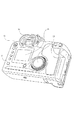
図1〜3を参照して、本発明の実施の形態に係るデジタル一眼レフカメラについて説明する。図1および図2は、本実施の形態に係るデジタル一眼レフカメラの外観図である。図1は、カメラを前面側(被写体側)から見た斜視図であって、撮影レンズユニットを外した状態を示す。図2は、カメラを撮影者側(背面側)から見た斜視図である。
<Camera configuration>
With reference to FIGS. 1-3, the digital single-lens reflex camera which concerns on embodiment of this invention is demonstrated. 1 and 2 are external views of a digital single-lens reflex camera according to the present embodiment. FIG. 1 is a perspective view of the camera viewed from the front side (subject side), and shows a state in which the taking lens unit is removed. FIG. 2 is a perspective view of the camera as viewed from the photographer side (back side).
図1に示すように、カメラ本体1には、撮影時に撮影者が安定して握り易いように被写体側に突出したグリップ部1aが設けられている。 As shown in FIG. 1, the camera body 1 is provided with a grip portion 1 a that protrudes toward the subject side so that the photographer can stably grip the camera body during shooting.
カメラ本体1のマウント部2には、撮影レンズユニット(図1、2では不図示)が着脱可能に固定される。マウント接点21は、カメラ本体1と撮影レンズユニットとの間で制御信号、状態信号、データ信号等の通信を可能にすると共に、撮影レンズユニット側に電力を供給する。マウント接点21は、電気通信のみならず、光通信、音声通信等が可能なように構成してもよい。マウント部2の横には、撮影レンズユニットを取り外す際に押し込むレンズロック解除ボタン4が配置されている。
A photographic lens unit (not shown in FIGS. 1 and 2) is detachably fixed to the
カメラ本体1内には、撮影レンズを通過した撮影光束が導かれるミラーボックス5が設けられており、ミラーボックス5内にメインミラー(クイックリターンミラー)6が配設されている。メインミラー6は、撮影光束をペンタダハミラー22(図3を参照)の方向へ導くために撮影光軸に対して45°の角度に保持される状態と、撮像素子33(図3を参照)の方向へ導くために撮影光束から退避した位置に保持される状態とを取り得る。
In the camera body 1, there is provided a
カメラ上部のグリップ1a側には、撮影開始の起動スイッチとしてのレリーズボタン7と、撮影時の動作モードに応じてシャッタスピードやレンズ絞り値を設定するためのメイン操作ダイヤル8と、撮影系の上面動作モード設定ボタン10とが配置されている。これら操作部材の操作結果の一部は、LCD表示パネル9に表示される。レリーズボタン7は、第1ストロークでSW1(図3の7a)がONし、第2ストロークでSW2(図3の7b)がONする構成となっている。また、上面動作モード設定ボタン10は、レリーズボタン7の1回の押込みで連写になるか1コマのみの撮影となるかの設定や、セルフ撮影モードの設定等を行うためのものであり、LCD表示パネル9にその設定状況が表示される。
On the grip 1a on the upper side of the camera, a release button 7 as a start switch for shooting, a main operation dial 8 for setting a shutter speed and a lens aperture value according to an operation mode at the time of shooting, and an upper surface of the shooting system An operation
カメラ上部の中央には、カメラ本体1に対してポップアップするストロボユニット11と、フラッシュ取り付け用のシュー溝12およびフラッシュ接点13とが設けられている。
A
カメラ上部の右寄りには、撮影モード設定ダイヤル14が配置されている。
A shooting
カメラのグリップ1aに対して反対側の側面には、開閉可能な外部端子蓋15が設けられている。外部端子蓋15を開けた内部には、外部インタフェースとしてビデオ信号出力用ジャック16およびUSB出力用コネクタ17が納められている。
An
図2に示すように、カメラ背面の上方には、ファインダ接眼窓18が設けられている。また、カメラ背面の中央付近には、画像表示可能なカラー液晶モニタ19が設けられている。
As shown in FIG. 2, a
カラー液晶モニタ19の横には、サブ操作ダイヤル20が配置されている。サブ操作ダイヤル20は、メイン操作ダイヤル8の機能の補助的役割を担うものである。例えばカメラのAEモードでは、自動露出装置により算出された適正露出値に対する露出補正量を設定するために使用される。シャッタスピードおよびレンズ絞り値の各々を使用者の意志により設定するマニュアルモードでは、メイン操作ダイヤル8でシャッタスピードを設定し、サブ操作ダイヤル20でレンズ絞り値を設定するように使用される。また、このサブ操作ダイヤル20は、カラー液晶モニタ19に表示される撮影済み画像の表示を選択するためにも使用される。
A
さらに、カメラ背面には、カメラの動作を起動もしくは停止するためのメインスイッチ43と、クリーニングモードを動作させるためのクリーニング指示操作部材44とが配置されている。クリーニング指示操作部材44は、詳しくは後述するが、光学ローパスフィルタ410の表面に付着した塵埃等の異物をふるい落とす動作を指示するためのものである。なお、クリーニングモードは、クリーニング指示操作部材44を用いて任意に動作させることもできるし、メインスイッチ43をONした際、或いはOFFした際、或いはその両方のタイミングで自動で動作させることもできる。
Further, a main switch 43 for starting or stopping the operation of the camera and a cleaning
図3は、本実施の形態に係るデジタル一眼レフカメラの主要な電気的構成を示すブロック図である。なお、図1、2と共通する部分には同一の符号を付す。カメラ本体1に内蔵されたマイクロコンピュータからなる中央処理装置(以下、「MPU」と称する)100は、カメラの動作制御を司るものであり、各要素に対して様々な処理や指示を実行する。MPU100に内蔵されたEEPROM100aは、時刻計測回路109の計時情報やその他の情報を記憶することができる。
FIG. 3 is a block diagram showing the main electrical configuration of the digital single-lens reflex camera according to the present embodiment. In addition, the same code | symbol is attached | subjected to the part which is common in FIG. A central processing unit (hereinafter, referred to as “MPU”) 100 formed of a microcomputer built in the camera body 1 controls operation of the camera, and executes various processes and instructions for each element. The EEPROM 100a built in the MPU 100 can store time information of the
MPU100には、ミラー駆動回路101、焦点検出回路102、シャッタ駆動回路103、映像信号処理回路104、スイッチセンス回路105、測光回路106が接続されている。また、LCD駆動回路107、バッテリチェック回路108、時刻計測回路109、電力供給回路110、圧電素子駆動回路111、振動検出回路112が接続されている。これらの回路は、MPU100の制御により動作するものである。
Connected to the MPU 100 are a
MPU100は、撮影レンズユニット200a内のレンズ制御回路201とマウント接点21を介して通信を行う。マウント接点21は、撮影レンズユニット200aが接続されるとMPU100へ信号を送信する機能も有する。これにより、レンズ制御回路201は、MPU100との間で通信を行い、AF駆動回路202および絞り駆動回路203を介して撮影レンズユニット200a内の撮影レンズ200および絞り204の駆動を行う。なお、図3では便宜上1枚の撮影レンズ200のみを図示しているが、実際は多数のレンズ群によって構成される。
The MPU 100 communicates with the
AF駆動回路202は、例えばステッピングモータによって構成され、レンズ制御回路201の制御により撮影レンズ200内のフォーカスレンズ位置を変化させ、撮像素子33に撮影光束の焦点を合わせるように調整する。絞り駆動回路203は、例えばオートアイリス等によって構成され、レンズ制御回路201の制御により絞り204を変化させ、光学的な絞り値を得る。
The
メインミラー6は、図3に示す撮影光軸に対して45°の角度に保持された状態で、撮影レンズ200を通過する撮影光束をペンタダハミラー22へ導くと共に、その一部を透過させてサブミラー30へ導く。サブミラー30は、メインミラー6を透過した撮影光束を焦点検出センサユニット31へ導く。 The main mirror 6 guides the photographic light beam passing through the photographic lens 200 to the penta roof mirror 22 and transmits a part thereof while being held at an angle of 45 ° with respect to the photographic optical axis shown in FIG. Guide to submirror 30. The sub mirror 30 guides the photographic light beam transmitted through the main mirror 6 to the focus detection sensor unit 31.
ミラー駆動回路101は、例えばDCモータとギヤトレイン等によって構成され、メインミラー6を、ファインダにより被写体像を観察可能とする位置と、撮影光束から待避する位置とに駆動する。メインミラー6が駆動すると、同時にサブミラー30も、焦点検出センサユニット31へ撮影光束を導く位置と、撮影光束から待避する位置とに移動する。
The
焦点検出センサユニット31は、不図示の結像面近傍に配置されたフィールドレンズ、反射ミラー、2次結像レンズ、絞り、複数のCCDからなるラインセンサ等によって構成され、位相差方式の焦点検出を行う。焦点検出センサユニット31から出力される信号は、焦点検出回路102へ供給され、被写体像信号に換算された後、MPU100に送信される。MPU100は、被写体像信号に基づいて位相差検出法による焦点検出演算を行う。そして、デフォーカス量およびデフォーカス方向を求め、これに基づいて、レンズ制御回路201およびAF駆動回路202を介して撮影レンズ200内のフォーカスレンズを合焦位置まで駆動する。
The focus detection sensor unit 31 is composed of a field lens, a reflection mirror, a secondary imaging lens, a diaphragm, a line sensor composed of a plurality of CCDs, etc. arranged in the vicinity of an imaging surface (not shown), and a phase difference type focus detection. I do. A signal output from the focus detection sensor unit 31 is supplied to the focus detection circuit 102, converted into a subject image signal, and then transmitted to the MPU 100. The MPU 100 performs focus detection calculation by the phase difference detection method based on the subject image signal. Then, the defocus amount and the defocus direction are obtained, and based on this, the focus lens in the photographic lens 200 is driven to the in-focus position via the
ペンタダハミラー22は、メインミラー6により反射された撮影光束を正立正像に変換反射する。撮影者はファインダ光学系を介してファインダ接眼窓18から被写体像を観察することができる。ペンタダハミラー22は、撮影光束の一部を測光センサ23へも導く。測光回路106は、測光センサ23の出力を得て、観察面上の各エリアの輝度信号に変換し、MPU100に出力する。MPU100は、輝度信号に基づいて露出値を算出する。
The penta roof mirror 22 converts and reflects the photographing light beam reflected by the main mirror 6 into an erect image. The photographer can observe the subject image from the
シャッタユニット(フォーカルプレーンシャッタ)32は、撮影者がファインダにより被写体像を観察している時には、シャッタ先幕が遮光位置にあると共に、シャッタ後幕が露光位置にある。次いで、撮影時には、シャッタ先幕が遮光位置から露光位置へ移動する露光走行を行って被写体からの光を通過させ、撮像素子33で撮像を行う。所望のシャッタ秒時の経過後、シャッタ後幕が露光位置から遮光位置へ移動する遮光走行を行って撮影を完了する。フォーカルプレーンシャッタ32は、MPU100の指令を受けたシャッタ駆動回路103により制御される。
The shutter unit (focal plane shutter) 32 has a shutter front curtain in a light shielding position and a shutter rear curtain in an exposure position when a photographer observes a subject image with a finder. Next, at the time of shooting, the shutter front curtain travels from the light shielding position to the exposure position, passes light from the subject, and the
撮像ユニット400は、光学ローパスフィルタ410、圧電部材と複数の電極からなる圧電素子430、撮像素子33が後述する他の部品と共にユニット化されたものである。撮像素子33は、被写体像を光電変換するものであり、本実施の形態ではCMOSセンサが用いられるが、その他にもCCD等様々な撮像素子があり、いずれのものを採用してもよい。撮像素子33の前方に配置された光学ローパスフィルタ410は、水晶からなる1枚の複屈折板であり、その形状は矩形状である。
The
クランプ/CDS(相関二重サンプリング)回路34は、A/D変換する前の基本的なアナログ処理を行うものであり、クランプレベルを変更することも可能である。AGC(自動利得調整装置)35は、A/D変換する前の基本的なアナログ処理を行うものであり、AGC基本レベルを変更することも可能である。A/D変換器36は、撮像素子33のアナログ出力信号をデジタル信号に変換する。
The clamp / CDS (correlated double sampling) circuit 34 performs basic analog processing before A / D conversion, and the clamp level can be changed. The AGC (automatic gain adjusting device) 35 performs basic analog processing before A / D conversion, and can change the AGC basic level. The A / D converter 36 converts the analog output signal of the
映像信号処理回路104は、デジタル化された画像データに対してガンマ/ニー処理、フィルタ処理、モニタ表示用の情報合成処理等、ハードウエアによる画像処理全般を実行する。この映像信号処理回路104からのモニタ表示用の画像データは、カラー液晶駆動回路113を介してカラー液晶モニタ19に表示される。また、映像信号処理回路104は、MPU100の指示に従って、メモリコントローラ38を通じてバッファメモリ37に画像データを保存することもできる。さらに、映像信号処理回路104は、JPEG等の画像データ圧縮処理を行うこともできる。連写撮影等、連続して撮影が行われる場合は、一旦バッファメモリ37に画像データを格納し、メモリコントローラ38を通して未処理の画像データを順次読み出すこともできる。これにより、映像信号処理回路104は、A/D変換器36から入力されてくる画像データの速度に関わらず、画像処理や圧縮処理を順次行うことができる。
The video
メモリコントローラ38は、外部インタフェース40から入力される画像データをメモリ39に記憶し、メモリ39に記憶されている画像データを外部インタフェース40から出力する機能を有する。なお、外部インタフェース40は、図1におけるビデオ信号出力用ジャック16およびUSB出力用コネクタ17が相当する。メモリ39としては、カメラ本体に着脱可能なフラッシュメモリ等が用いられる。
The memory controller 38 has a function of storing the image data input from the external interface 40 in the memory 39 and outputting the image data stored in the memory 39 from the external interface 40. The external interface 40 corresponds to the video
スイッチセンス回路105は、各スイッチの操作状態に応じて入力信号をMPU100に送信する。スイッチSW1(7a)は、レリーズボタン7の第1ストローク(半押し)によりONする。スイッチSW2(7b)は、レリーズボタン7の第2ストローク(全押し)によりONする。スイッチSW1(7a)がONされると、撮影準備開始の指示がMPU100に送信され、スイッチSW2(7b)がONされると、撮影開始の指示がMPU100に送信される。また、メイン操作ダイヤル8、サブ操作ダイヤル20、撮影モード設定ダイヤル14、メインスイッチ43、クリーニング指示操作部材44が接続されている。
The
LCD駆動回路107は、MPU100の指示に従って、LCD表示パネル9やファインダ内液晶表示装置41を駆動する。 The LCD drive circuit 107 drives the LCD display panel 9 and the in-finder liquid crystal display device 41 in accordance with instructions from the MPU 100.
バッテリチェック回路108は、MPU100の指示に従って、バッテリチェックを行い、その検出結果をMPU100に送信する。電源42は、カメラの各要素に対して電源を供給する。 The battery check circuit 108 performs a battery check according to an instruction from the MPU 100 and transmits the detection result to the MPU 100. The power supply 42 supplies power to each element of the camera.
時刻計測回路109は、メインスイッチ43がOFFされて次にONされるまでの時間や日付を計測し、MPU100からの指示に従って、計測結果をMPU100に送信する。
The
<異物除去構造>
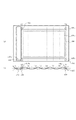
次に、図4〜6を参照して、本実施の形態における光学ローパスフィルタ410を加振する異物除去構造について説明する。図4は、撮像ユニット400まわり保持構造を示すためのカメラ内部の概略構成を示す分解斜視図である。図5は、撮像ユニット400の構成を示す分解斜視図である。
<Foreign matter removal structure>
Next, with reference to FIGS. 4-6, the foreign material removal structure which vibrates the optical low-
図4に示すように、カメラ本体の骨格となる本体シャーシ300の被写体側には、被写体側から順に、ミラーボックス5、シャッタユニット32が配設される。また、本体シャーシ300の撮影者側には、撮像ユニット400が配設される。撮像ユニット400は、撮影レンズユニットが取り付けられる基準となるマウント部2の取付面に撮像素子33の撮像面が所定の距離を空けてかつ平行になるように調整されて固定される。
As shown in FIG. 4, the
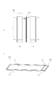
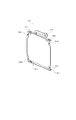
図5に示すように、光学ローパスフィルタ410は、水晶からなる1枚の複屈折板であり、その形状は矩形状である。この光学ローパスフィルタ410が本発明でいう被振動部材であり、撮像素子33の前方に配設された光学素子に相当するものである。光学ローパスフィルタ410は、撮影有効領域410aの一側方に圧電素子430を配置する周縁部410bを有しており、撮影光軸中心に対して直交する方向(カメラ左右方向)に非対称である。このように、撮影有効領域410aと周縁部410bとが重ならないように設定することで、被写体像の有効光束に圧電素子430が侵入しないように担保されている。
As shown in FIG. 5, the optical low-
また、このようにした光学ローパスフィルタ410の表面には、導電性を持たせるための導電コーティングと、反射防止膜などの光学的なコーティングが施されている。
The surface of the optical low-
圧電素子430は、後述するように1枚の圧電部材上に複数の電極が一体的に形成されており、短冊状の外形を有する。そして、光学ローパスフィルタ410の周縁部410bに、圧電素子430の長辺が光学ローパスフィルタ410の短辺(側辺)に平行になるように接着される。すなわち、圧電素子430は、光学ローパスフィルタ410の四辺のうち一辺近傍で平行に接着される。光学ローパスフィルタは、その一辺に平行な複数の腹部および節部が生じるように振動される。具体的な振動の様子については後述する。
As will be described later, the
420は樹脂製又は金属製の光学ローパスフィルタ保持部材であり、光学ローパスフィルタ410を保持し、撮像素子保持部材510にビス固定される。
An optical low-pass
470は圧電素子430に電圧を印加するための圧電素子用フレキシブルプリント基板であり、圧電素子430の各電極に接続される。
470 is a piezoelectric element flexible printed circuit board for applying a voltage to the
440は付勢部材であり、光学ローパスフィルタ410の撮影有効領域410a外の4ヶ所において当接して撮像素子33方向に付勢し(図12および図13を参照)、光学ローパスフィルタ保持部材420に係止される。付勢部材440は接地されており、付勢部材440と接する光学ローパスフィルタ410の表面(導電コーティングおよび光学的なコーティングが施された面)も接地される。これにより、光学ローパスフィルタ410の表面への塵埃等の静電気的な付着を抑制することができる。
450は断面が略円形の枠状の弾性部材であり、光学ローパスフィルタ410と光学ローパスフィルタ保持部材420とで挟まれて密着保持される。この密着力は、付勢部材440の撮像素子33方向への付勢力により決定される。なお、弾性部材450はゴムでもよいし、弾性体であれば、ポロンやプラスチック等の高分子重合体を用いてもよい。
460は位相板(偏光解消板)と、赤外カットフィルタと、光学ローパスフィルタ410に対して屈折方向が90°異なる複屈折板とを貼り合わせた光学部材であり、光学ローパスフィルタ保持部材420に接着固定される。
510は板状の撮像素子保持部材であり、矩形の開口部を有し、その開口部に撮像素子33を露出させるように撮像素子33が固着する。撮像素子保持部材510の周囲には、ミラーボックス5に3ヵ所でビス固定するための固定箇所が設けられている。
Reference numeral 510 denotes a plate-shaped image sensor holding member having a rectangular opening, and the
520は撮像素子33に撮影光路外からの余分な光が入射することを防ぐためのマスクであり、光学ローパスフィルタ保持部材420と撮像素子33とで挟まれて密着保持される。
530は左右一対の板バネ状の撮像素子付勢部材であり、撮像素子保持部材510にビス固定され、撮像素子33を撮像素子保持部材510に押し付ける。
以上の構成をとることにより、光学ローパスフィルタ410は、付勢部材440と弾性部材450とで挟み込まれて振動自在に支持される。詳しくは後述するが、光学ローパスフィルタ410の支持位置(支持部位)は、光学ローパスフィルタ410の振動の節部近傍であることが望ましい。なお、節部とは振幅がほぼ零となる位置のことをいう。
By adopting the above configuration, the optical low-
図6は、図4におけるA−A線断面図である。ただし、撮像素子保持部材510は省略してある。マスク520の撮影者側の面は撮像素子33と当接し、被写体側の面は光学ローパスフィルタ保持部材420と当接する。マスク520の撮影者側および被写体側にはそれぞれ両面テープが用いられている。光学ローパスフィルタ保持部材420は、マスク520の両面テープにより、撮像素子33に密閉固定保持される。また、光学部材460は、光学ローパスフィルタ保持部材420の所定の保持部に、外周部において接着されて保持される。これにより、光学ローパスフィルタ保持部材420と撮像素子33とマスク520と光学部材460とにより囲まれる空間は封止され、塵埃等の異物の侵入を防ぐ密閉空間が形成される。
6 is a cross-sectional view taken along line AA in FIG. However, the image sensor holding member 510 is omitted. The surface on the photographer side of the
一方、弾性部材450の撮影者側の面は光学ローパスフィルタ保持部材420と当接し、被写体側の面は光学ローパスフィルタ410と当接する。光学ローパスフィルタ410は付勢部材440の弾性により撮像素子33方向へと付勢されているので、弾性部材450は変形し、光学ローパスフィルタ410および光学ローパスフィルタ保持部材420に対して隙間無く密着する。これにより、光学ローパスフィルタ410と光学ローパスフィルタ保持部材420と弾性部材450と光学部材460とにより囲まれる空間は封止され、塵埃等の異物の侵入を防ぐ密閉空間が形成される。
On the other hand, the surface on the photographer side of the
<圧電素子の電極配置>
図7(a)、図7(b)、図8(a)および図8(b)は、圧電素子430の詳細を説明するための図である。このうち、図7(a)および図7(b)は、電極の配置を最も簡略化した場合を説明するための図であり、図8(a)および図8(b)は、本実施の形態においてより好ましい電極の配置を説明するための図である。
<Electrode arrangement of piezoelectric element>
FIGS. 7A, 7 </ b> B, 8 </ b> A, and 8 </ b> B are diagrams for explaining details of the
まずは、電極の配置を最も簡略化した場合について説明する。図7(a)は、圧電素子430の表面(第一面側、ここではF面とする)と、裏面(第二面側、ここではB面とする)と、側面を示す図であり、図7(b)は、F面側から見た場合の斜視図である。図示するように、圧電素子430は、1枚のピエゾ素子である圧電部材430aと、この上に設けられた4つの電極である、電極AF、電極AB、電極SF、電極SBから成る。
First, the case where the arrangement of the electrodes is most simplified will be described. FIG. 7A is a diagram showing a front surface (first surface side, here F surface), a back surface (second surface side, here B surface), and a side surface of the
このうち電極AFと電極ABは、圧電部材430aを挟んで対向して配置された、光学ローパスフィルタ410に定在波を励起させるための駆動電極(第一駆動電極、第二駆動電極)である。制御回路である圧電素子駆動回路111が、これらの電極に交互に電圧を印加することにより、矢印Y方向と平行な節と腹を複数有する定在波振動を発生させる。
Among these, the electrode AF and the electrode AB are drive electrodes (first drive electrode, second drive electrode) that are disposed to face each other with the
また、電極SFは、圧電部材430a、ひいては光学ローパスフィルタ410に発生した振動を検出するための振動検出電極である。具体的には、この電極SFに圧電部材430aを挟んで対向して設けられた、常時接地されたグランド電極である電極SBに対して、電極SFの発生する電荷電圧がどのように変化するかを監視して振動を検出する。
Further, the electrode SF is a vibration detection electrode for detecting vibration generated in the
駆動電極である電極AFと電極ABは、光学ローパスフィルタに定在波振動を発生させるための電極なので、大きな駆動力を得るために、電極SFと電極SBに対して相対的にできる限り大きいことが好ましい。また、振動検出電極である電極SFは、駆動電極によって発生された定在波振動を適切に捉えるため、定在波の節と腹が発生する方向である矢印Y方向(節方向、もしくは腹方向)に直交する矢印X方向が、長辺方向となるような形状が望ましい。 The electrodes AF and AB, which are drive electrodes, are electrodes for generating standing wave vibration in the optical low-pass filter, so that they are as large as possible relative to the electrodes SF and SB in order to obtain a large drive force. Is preferred. In addition, the electrode SF as a vibration detection electrode appropriately captures the standing wave vibration generated by the driving electrode, and thus the arrow Y direction (node direction or antinode direction), which is a direction in which standing wave nodes and antinodes are generated. A shape in which the direction of the arrow X perpendicular to the long side direction is desirable.
それぞれの電極は、独立して圧電素子用フレキシブルプリント基板470に接続される。そして、圧電素子用フレキシブルプリント基板470の配線を介して、駆動電極である電極AFと電極ABは圧電素子駆動回路111に、振動検出電極である電極SFは振動検出回路112に、電極SBはグランドに接続される。
Each electrode is independently connected to the flexible printed
このように構成された圧電素子430は、上述のように、光学ローパスフィルタ410の周縁部410bにB面もしくはF面が接着されて固定される。
As described above, the
圧電素子430が接着される光学ローパスフィルタ410の周辺部410bについては、圧電素子430の駆動力をロスしないように、つまり、直接ローパスフィルタに接触するように、導電コーティングや光学的なコーティングを施さないことが望ましい。ただし、グランド電極である電極SBが接触する領域については、撮影有効領域410aから導電コーティングを伸延して電極SBと導通するように構成すれば、撮影有効領域410aの接地が安定するので、より好ましいと言える。
The peripheral portion 410b of the optical low-
次に、本実施の形態においてより好ましい電極の配置について説明する。図8(a)は、圧電素子430の表面(図7と同様にF面とする)と、裏面(同じく図7と同様にB面とする)と、側面を示す図であり、図8(b)は、F面側か見た場合の斜視図である。図示するように、圧電素子430は、1枚のピエゾ素子である圧電部材430aと、この上に設けられた6つの電極である、電極AF、電極AB、電極SF、電極SB、電極AB’、電極SB’から成る。
Next, a more preferable arrangement of electrodes in the present embodiment will be described. FIG. 8A is a diagram showing the front surface (referred to as F surface as in FIG. 7), the back surface (also referred to as B surface as in FIG. 7), and the side surface of the
電極AFと電極ABが駆動電極であり、電極SFが振動検出電極であり、電極SBが常時接地されたグランド電極であることは、図7で示した圧電素子430と同様である。
The electrode AF and the electrode AB are drive electrodes, the electrode SF is a vibration detection electrode, and the electrode SB is a ground electrode that is always grounded, as in the
ただし、図7で示した圧電素子430と異なり、B面の電極ABと電極SBは、それぞれスルーホールABTとスルーホールSBTにより、F面側に設けられた電極AB’と電極SB’にそれぞれ導通されている。
However, unlike the
このように構成することで、駆動電極と振動検出電極とグランド電極は、全てF面側から引き出して圧電素子用フレキシブルプリント基板470に接続することができる。したがって、ユニットの組み立て作業性に大いに貢献する。同時に、光学ローパスフィルタ410の周縁部410bにB面を接着して固定する観点からも、接着面の凹凸を避けることができるので、接着性のみならず、ひいては光学ローパスフィルタ410の振動効率の向上にも寄与する。なぜなら、接着面にはフレキシブルプリント基板470が接続されることがないので、その厚みによる段差が生じないからである。
With this configuration, all of the drive electrode, the vibration detection electrode, and the ground electrode can be drawn out from the F-plane side and connected to the flexible printed
<振動の説明>
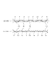
次に、図9を参照して、光学ローパスフィルタ410の異物を除去する動作としての振動の様子について説明する。図9は、撮像ユニット400のうち光学ローパスフィルタ410、およびこれにB面側が接着されて一体的に設けられた圧電素子430のみを取り出して示した側面図である。図9は、圧電素子430に駆動電圧を印加した際の光学ローパスフィルタ410および圧電素子430の状態変化(振動形状)を表している。
<Description of vibration>
Next, with reference to FIG. 9, the state of vibration as an operation of removing the foreign matter of the optical low-
圧電素子用フレキシブルプリント基板470を通じて圧電素子430の電極AFに正の電圧を印加し、電極ABをグランド(0[V])としたとする。このとき、圧電素子430は面方向に伸びて、厚み方向に縮む。すると、圧電素子430と接着された光学ローパスフィルタ410は、接着面が拡大する方向に力を受ける。このような力を受けると、光学ローパスフィルタ410を断面方向から見た場合、圧電素子430側の面が伸びる方向に変形し、対向面が縮む方向に変形するので、圧電素子430を頂点に乗せた凸形状となる。この変形が連鎖して、光学ローパスフィルタ410を断面方向から見ると、凹凸形状が連続した屈曲変形が生じる。すなわち、電極AFに正の電圧が印加されると、光学ローパスフィルタ410には図9の実線で示すような屈曲変形が生じる。
It is assumed that a positive voltage is applied to the electrode AF of the
同様に、電極ABに正の電圧を印加し、電極AFをグランド(0[V])としたとき、圧電素子430は面方向に縮み、厚み方向に伸びる。すると、圧電素子430と接着された光学ローパスフィルタ410は、接着面が収縮する方向に力を受ける。このような力を受けると、光学ローパスフィルタ410を断面方向から見た場合、圧電素子430側の面が縮む方向に変形し、対向面が伸びる方向に変形するので、圧電素子430を内側に抱え込んだ凹形状となる。すなわち、電極AFに正の電圧を印加したときとは逆向きの変形を生じ、光学ローパスフィルタ410には、図9の破線に示すような屈曲変形が生じる。
Similarly, when a positive voltage is applied to the electrode AB and the electrode AF is set to the ground (0 [V]), the
したがって、電極AFに正の電圧を印加し電極ABをグランドとする状態と、電極ABに正の電圧を印加し電極AFをグランドとする状態とを、交互に周期的に切り替えると定在波振動が生じることになる。つまり、圧電部材430aの作用により、図9の実線の状態と破線の状態を交互に繰り返す、周期的な振動を生じることになる。この周期的な電圧の周波数は、光学ローパスフィルタ410の固有モードの共振周波数近傍とすることで、小さな印加電圧でも大きな振幅を得ることができ効率がよい。また、光学ローパスフィルタ410の共振周波数は複数存在し、各々の共振周波数で電圧を印加すると各々異なる次数の振動モードで振動させることができる。図9では、腹が7つ生じる7次振動モードと、8つ生じる8次振動モードを示している。
Therefore, when the positive voltage is applied to the electrode AF and the electrode AB is grounded, and the state in which the positive voltage is applied to the electrode AB and the electrode AF is grounded are alternately alternately switched, the standing wave vibration is generated. Will occur. In other words, the action of the
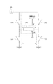
ここで、図10および図11を用いて、圧電素子430とその駆動回路および駆動方法について説明する。図10は、制御回路である圧電素子駆動回路111と圧電素子430の概略説明図である。図11は、図10の圧電素子駆動回路111の動作と、振動検出回路112の検出結果を説明するための動作波形図である。
Here, the
圧電素子駆動回路111は、図10に示すように、+Vの電圧を与える直流電源600とスイッチング素子610a〜610d、そしてこのスイッチング素子610a〜610dの周期的なスイッチングをおこなう不図示の制御部から構成される。制御部は、包含するパルス発生回路の駆動パルスに応じて一定の周期を生成し、スイッチングを行う。
As shown in FIG. 10, the piezoelectric element driving circuit 111 includes a
そして、圧電部材430aには、上述のように駆動電極である電極AF、電極BFと、振動検出電極である電極SFと、グランド電極である電極SBが設けられている。このうち、電極AFはスイッチング素子610aと610bに接続されており、電極ABはスイッチング素子610cと610dに接続されている。電極SFは振動検出回路112と接続されている。また、直流電源600には、スイッチング素子610aと610cが接続されており、グランドには電極SBとスイッチング素子610bと610dが接続されている。このように接続することで、Hブリッジ(フルブリッジ)のスイッチング回路を構成している。なお、スイッチング素子としてはMOSFETが一般的だが、バイポーラトランジスタなどの他の半導体素子や制御可能な機械接点を用いてもよい。
The
振動検出回路112は、圧電部材の伸縮によって生じる電位差を検出する回路である。 The vibration detection circuit 112 is a circuit that detects a potential difference caused by expansion and contraction of the piezoelectric member.
図11に示す5つのタイミングチャートは、いずれも横軸が経過時間であり、縦軸が電圧である。電極AFおよび電極ABには、図示するように、パルス発生回路の駆動パルスにより、交互に+Vと0を繰り返す方形波が印加される。制御部によりスイッチング素子610aおよび610dがONされ、スイッチング素子610bおよび610cがOFFされると、一点鎖線Iaのように電流が流れ、電極AFは電圧+V、電極ABは電圧0となる。逆に、スイッチング素子610bおよび610cがONされ、スイッチング素子610aおよび610dがOFFされると、点線Ibのように電流が流れ、電極AFは電圧0、電極ABは電圧+Vとなる。この動作を光学ローパスフィルタ410の共振周波数で繰り返すことで、圧電素子430を振動させている。
In each of the five timing charts shown in FIG. 11, the horizontal axis represents elapsed time, and the vertical axis represents voltage. As shown in the figure, a square wave that alternately repeats + V and 0 is applied to the electrode AF and the electrode AB by the drive pulse of the pulse generation circuit. When switching
このとき、圧電素子430の駆動電圧は、実質的に電極ABに対する電極AFの電圧(電極AFの電圧から電極ABの電圧を差し引いた電圧)となるので、図11のAB基準AFに示すように+Vと−Vを交互に繰り返す。したがって、電源電圧の2倍の電位差で駆動することができる。換言すると、駆動電圧を同じにすることを考えると、Hブリッジ回路はハーフブリッジ回路に比べ、電源電圧が1/2で済む。Hブリッジ回路を適用すれば、電源電圧を小さくできることから回路素子の耐圧レベルを下げることができ、回路の小型化、コストダウンに有効である。
At this time, since the driving voltage of the
電極SFを用いた振動状態の検出については後述する。 The detection of the vibration state using the electrode SF will be described later.
図9に戻り、振動の様子について説明を続ける。 Returning to FIG. 9, the description of the state of vibration will be continued.
上述のように、圧電素子430の伸縮により光学ローパスフィルタ410に定在波振動が発生する。図9に示すように、定在波振動では振動の節部(d1、d2、・・・、D1、D2、・・・)と腹部とが交互に生じる。振動の節部とは振幅がほぼ零となる位置であり、振動の腹部とは隣り合う節部間において振幅が最大となる位置である。光学ローパスフィルタ410の表面に付着した塵埃等をふるい落とすには、付着力以上の力が発生するように加速度を塵埃等に加えなければならない。ところが、振動の節部では振幅がほぼ零であることから発生する加速度もほぼ零であり、付着力に抗して塵埃等をふるい落とすことができない。そのため、1つの振動モードだけで光学ローパスフィルタ410を振動させると、振動の節部上に塵埃等が残ってしまう。
As described above, standing wave vibration is generated in the optical low-
この点を改善するため、ある振動モードで光学ローパスフィルタ410を振動させた後、もう1つ別の振動モードで光学ローパスフィルタ410を振動させるように圧電素子430を制御する。これにより、最初の振動モードで残った塵埃等を、その後の別の振動モードで除去することができる。この場合に、ある振動モードでの節部ともう1つ別の振動モードでの節部とが重なってしまうと、その重なった節部の塵埃等が除去できないため、節部は重ならないようにしなければならない。したがって、使用する振動モードの組合せは偶数節(奇数次)および奇数節(偶数次)であることが望ましい。本実施の形態では、7次振動モード(8節)および8次振動モード(9節)を組み合わせて使用している。
In order to improve this point, after the optical low-
なお、光学ローパスフィルタ410の共振周波数は、光学ローパスフィルタ410の形状、板厚、材質等により異なるが、不快な音の発生を抑えるべく、可聴域外となるような共振周波数を選ぶことが好ましい。本実施の形態では7次振動モードおよび8次振動モードで振動を発生させる例を説明したが、これに限らず、他の次数の振動モードで振動を発生させるようにしても良いし、3種類以上の振動モードを用いても良い。
Although the resonance frequency of the optical low-
<光学ローパスフィルタ410の支持構成>
図12は、光学ローパスフィルタ410および圧電素子430の振動形状と光学ローパスフィルタ410の支持位置を説明するための図である。なお、本実施の形態では7次振動モードおよび8次振動モードで振動を発生させるが、図12では8次振動モードでの振動形状を表している。この定在波振動は、圧電素子430の長辺に略平行に節部と腹部が発生する。
<Supporting configuration of optical low-
FIG. 12 is a diagram for explaining the vibration shape of the optical low-
図12(b)に示すように、光学ローパスフィルタ410は、付勢部材440と弾性部材450とで挟み込まれる(サンドイッチされる)ように支持されている。
As shown in FIG. 12B, the optical low-
ここで、図13を用いて付勢部材440の形状について説明する。図13は、付勢部材440の斜視図である。付勢部材440は、薄板のステンレス材を打ち抜き、折り曲げて成形されるものであり、全体で板バネとしての性質を有する。そして、光学ローパスフィルタ410の表面に対し、4箇所で当接するように接触点440aがそれぞれ窪ませて形成され、爪部440cで光学ローパスフィルタ保持部材420に係止されることで、光学ローパスフィルタ410を撮像素子33側へ付勢する。つまり、付勢部材440は、4箇所の接触点440aのみで光学ローパスフィルタ410を被写体側から支えていることになる。なお、440bは、光学ローパスフィルタ410の表面をグランド(0[V])に接続するための接地部である。
Here, the shape of the biasing
図12に戻り、図12(a)に示すように、光学ローパスフィルタ410は、付勢部材440とは撮影有効領域410a外の4ヶ所の接触点440aにおいて当接し、弾性部材450とは撮影有効領域410a外において矩形状に密着当接する。
Returning to FIG. 12, as shown in FIG. 12A, the optical low-
一般的に、振動している物体に物が当接すると振動が減衰してしまうが、振幅がほぼ零である振動の節部に物が当接する場合は、振動の減衰は緩和される。そこで、付勢部材440が光学ローパスフィルタ410に当接する4ヶ所(接触点440a)、および、弾性部材450が光学ローパスフィルタ410に当接する矩形状部分のうち節部と平行な二辺は、振動の節部(図示例では節部D2、D9)近傍に配設される。節部だけでなく、節部近傍も振幅が小さいことから、光学ローパスフィルタ410の振動の減衰は緩和される。これにより、光学ローパスフィルタ410の異物除去能力を落とさずに、光学ローパスフィルタ410を支持することができる。
Generally, when an object comes into contact with a vibrating object, the vibration is attenuated. However, when an object comes into contact with a vibration node having an amplitude of almost zero, the attenuation of the vibration is alleviated. Therefore, four places (
また、本実施の形態のように、略矩形部材である光学ローパスフィルタ410の一辺(短辺)に平行な方向にのみ節部を発生させる振動モードにおいて、この節部の発生箇所は非常に明解である。図14は、光学ローパスフィルタ410単体時における振動形状を表しており、特に8次振動モードでの振動形状を表している。図14(a)の点線部は、振動の節部を表している。
Further, in the vibration mode in which the nodal portion is generated only in the direction parallel to one side (short side) of the optical low-
図14に示すように、光学ローパスフィルタ410の振動の節部は、光学ローパスフィルタ410の両短辺(節部に対して平行な二辺)から1/4波長だけ内側にそれぞれ発生し、さらにその内側には1/2波長ごとに発生する。なお、波長とは、隣り合う同位相の腹部の間隔(波の山から次の山(又は谷から次の谷)までの水平距離)のことであり、図14に示す距離λである。よって、光学ローパスフィルタ410を支持する位置は、圧電素子430を配置している側(加振側)においては圧電素子接着位置から撮影光軸側で圧電素子430に最も近い節部(図12の節部D2)近傍であることが望ましい。また、圧電素子430を配置していない側(自由端側)においては端から1/4波長だけ内側の節部(図12の節部D9)近傍であることが望ましい。この場合、上述の節部近傍とは、1/8波長から3/8波長の範囲であることが実験的に確認されており、この範囲で支持すれば、光学ローパスフィルタ410の振動の減衰は緩和され、異物除去能力は阻害されない。
As shown in FIG. 14, the vibration nodes of the optical low-
特に圧電素子430を配置していない側(自由端側)の振動においては、節部以外を支持すると振幅が大きく減衰してしまい、塵埃等の除去に必要な力(加速度)を発生させることができなくなるため、節部を外すことなく支持することが非常に重要である。一方、圧電素子430を配置している側(加振側)の振動においては、加振源(圧電素子430)が近傍にあるので、節部以外を支持することによる振幅の減衰は、自由端における振幅の減衰と比較して小さい。
In particular, in the vibration on the side where the
また、図12に示すように、圧電素子430の接着固定位置は、光学ローパスフィルタ410に発生させる振動モードでの振動の腹部を含む、すなわち、節部間の中心線上に重なるように固着されるのが望ましい。さらに、圧電素子430の短辺方向(振動の節部に対して直交する方向)の長さ(幅)は、発生させる振動モードでの波長λの1/2以下であることが望ましい。圧電素子430の電圧印加により伸縮する部分と、光学ローパスフィルタ410の振動の腹部とを合致させて接着することで、光学ローパスフィルタ410の定在波振動を阻害することなく、小さな印加電圧で大きな振幅を効率良く発生させることができるからである。
Also, as shown in FIG. 12, the adhesive fixing position of the
なお、本発明でいう光学部材は光学ローパスフィルタ410に限定されるものではない。例えば、本実施の形態では水晶複屈折板に定在波振動を励起する構成としたが、複屈折板の材質は水晶ではなくニオブ酸リチウムを用いてもよい。また、複屈折板と位相板と赤外吸収フィルタの貼り合わせによって構成される光学ローパスフィルタや赤外吸収フィルタ単体に定在波振動を励起する構成にしても良い。また、複屈折板の前に配置したガラス板単体に定在波振動を励起する構成にしても良い。
The optical member referred to in the present invention is not limited to the optical low-
<振動状態の検出>
図11に戻り、圧電素子430の振動状態の検出について説明する。圧電素子430の振動に伴って、圧電効果により電極SFには正弦波の電圧が発生する。このとき、電極SBは常にグランド(0[V])に保たれているので、振動検出回路112により、図11の「SB基準SF」に示される正弦波形が得られる。ここで検出される+vd[V]と−vd[V]の電位差は、圧電素子430の、ひいては光学ローパスフィルタ410の振動振幅に比例するものである。したがって、「SB基準SF」の電圧波形(振動検出波形)を監視することで、圧電素子430の、ひいては光学ローパスフィルタ410の振動状態を検出することが可能となる。
<Detection of vibration state>
Returning to FIG. 11, detection of the vibration state of the
この振動状態を検出することで以下の2つのことが行える。 The following two things can be performed by detecting this vibration state.
まず1つは共振周波数の検出である。これまでに述べたように、光学ローパスフィルタ410は共振周波数で振動させることが望ましい。本実施例では、7次振動モードと8次振動モードの共振周波数を探し出し、その共振周波数でもって圧電素子430を振動させる必要がある。そのために、あらかじめ理論値および設計/組み立てのバラツキを考慮し、共振周波数の存在する周波数帯域を決定し、その範囲内で圧電素子430の駆動周波数を徐々に変化させて、振動検出波形の振幅が最大となる周波数を探し出す。そして、その共振周波数を含む所定の周波数帯域を圧電素子の駆動周波数として用い、光学ローパスフィルタ410を振動させる。この共振周波数の検出動作は、工場での量産工程内で行うことはもとより、ユーザ使用時においても行うことが可能である。これにより、カメラの使用環境や経時変化にも対応した、共振周波数をもって光学ローパスフィルタ410を振動させ、異物除去動作を行うことができる。したがって、振動検出回路112は、共振周波数検出回路として機能する。
One is detection of the resonance frequency. As described above, it is desirable to vibrate the optical low-
もう1つは故障検知もしくは異常検知である。上記の共振周波数の検出動作時において、検出される振幅が想定される振幅を大幅に下回る場合や、振動検出波形が異常な形を示す場合、この異物除去ユニットが異常であると認識でき、異物除去ユニットの動作停止および交換などの対処を施すことが出来る。 The other is failure detection or abnormality detection. If the detected amplitude is significantly lower than the assumed amplitude or the vibration detection waveform shows an abnormal shape during the above-described resonance frequency detection operation, this foreign matter removal unit can be recognized as abnormal. It is possible to take measures such as stopping and replacing the removal unit.
<異物除去動作>
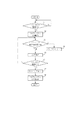
次に、図15を参照して、光学ローパスフィルタ410の表面に付着した塵埃等の異物を除去する動作について説明する。ステップS1で、メインスイッチ43により電源がONされたか否かを判定する。電源がONされると、ステップS2で、カメラシステムを起動させるための処理を行い、電力供給回路110を制御して各回路へ電力を供給し、システムを初期設定し、カメラとして撮影動作可能にするためのカメラシステムON動作を行う。
<Foreign matter removal operation>
Next, with reference to FIG. 15, an operation for removing foreign matters such as dust attached to the surface of the optical low-
次に、ステップS3で、撮影者によりクリーニング指示操作部材44が操作されたか否かを判定し、操作されている場合はステップS4に進み、操作されていない場合はステップS5へ進む。なお、本実施の形態ではクリーニング指示操作部材44を設けたが、本発明はこれに限定されるものではない。例えば、クリーニングモードへの移行を指示するための操作部材は、機械的なボタンに限らず、カラー液晶モニタ19に表示されたメニューから、カーソルキーや指示ボタン等を用いて指示するものであっても良い。
Next, in step S3, it is determined whether or not the cleaning
ステップS4では、クリーニングモード開始の指令を受けて、カメラ本体1をクリーニングモードの状態に移行させる。まず電力供給回路110は、クリーニングモードに必要な電力をカメラ本体1の各部へ供給する。また、これに並行して電源42の電池残量を検出して、その結果をMPU100へ送信する。MPU100は、クリーニングモード開始の信号を受け取ると、圧電素子駆動回路111に駆動指示を送る。圧電素子駆動回路111は、MPU100より駆動指示を受け取ると、光学ローパスフィルタ410の定在波振動を励起する周期電圧を生成し、圧電素子430に印加する。圧電素子430は、上述のように、印加される電圧に応じて伸縮し、光学ローパスフィルタ410に定在波振動を発生させる。クリーニングモードが終了するとステップS5に進む。
In step S4, in response to the instruction to start the cleaning mode, the camera body 1 is shifted to the cleaning mode. First, the power supply circuit 110 supplies power necessary for the cleaning mode to each part of the camera body 1. In parallel with this, the remaining battery level of the power source 42 is detected, and the result is transmitted to the MPU 100. Upon receiving the cleaning mode start signal, the MPU 100 sends a drive instruction to the piezoelectric element drive circuit 111. When the piezoelectric element driving circuit 111 receives a driving instruction from the MPU 100, the piezoelectric element driving circuit 111 generates a periodic voltage that excites the standing wave vibration of the optical low-
ステップS5で、スイッチSW1(7a)、スイッチSW2(7b)、メイン操作ダイヤル8、サブ操作ダイヤル20、撮影モード設定ダイヤル14、他のスイッチ等の信号を受け、カメラ動作を行う。カメラ動作は、一般的に知られるカメラの撮影/設定等を行うモードで、ここでは詳細な説明は省略する。
In step S5, signals from the switch SW1 (7a), the switch SW2 (7b), the main operation dial 8, the
次に、ステップS6で、カメラが待機状態においてメインスイッチ43にて電源がOFFされたか否かを判定し、OFFされるとステップS7に進み、OFFされていなければステップS3に戻る。 Next, in step S6, it is determined whether the power is turned off by the main switch 43 when the camera is in a standby state. If turned off, the process proceeds to step S7, and if not turned off, the process returns to step S3.
ステップS7では、ステップS4と同様のクリーニングモードを実行後、ステップS8に進む。ここで、ステップS7におけるクリーニングモードでは、カメラの消費電力、動作時間等を考慮して、圧電素子430の駆動周波数、駆動時間、制御法等のパラメータをステップS4と異ならしめても良いことは言うまでも無い。
In step S7, after executing the same cleaning mode as in step S4, the process proceeds to step S8. Here, in the cleaning mode in step S7, parameters such as the driving frequency, driving time, and control method of the
ステップS8では、MPU100の制御により各回路を終了させるための制御を行い、必要な情報等をEEPROM100aに格納し、電力供給回路110を制御して各回路への電源供給を遮断する電源OFF動作を行う。 In step S8, control for terminating each circuit is performed under the control of the MPU 100, necessary information is stored in the EEPROM 100a, and the power supply circuit 110 is controlled to shut off the power supply to each circuit. Do.
以上述べたように、撮影者が意図した任意のタイミングだけではなく、電源をOFFするとクリーニングモードが実行される。すなわち、光学ローパスフィルタ410の表面に付着した異物を除去する動作を行ってから、カメラシステムOFF動作を行うようにしている。
As described above, the cleaning mode is executed not only at an arbitrary timing intended by the photographer but also when the power is turned off. That is, the camera system OFF operation is performed after the operation of removing the foreign matter adhering to the surface of the optical low-
ここで、光学ローパスフィルタ410の表面に付着した異物には様々なものが存在するが、一般的に異物が付着した状態で長期間放置すると、クリーニングモードで振動をかけても除去しにくいことが実験的に解明した。これは、環境(温度や湿度)の変化で結露することにより液架橋力等の付着力が増大したり、環境の変化で塵埃が膨潤、乾燥を繰り返すことにより粘着したりすることによるものと考えられる。また、ゴム等の弾性材では、自身に含まれる油脂等が時間と共にブリードして粘着する。そのため、電源OFF操作のタイミングでクリーニングモードを実行することが、異物を除去しにくい状態になっている可能性の高い長期間未使用状態後の電源ON操作のタイミングで行うよりも、より効率的・効果的である。
Here, there are various kinds of foreign matters attached to the surface of the optical low-
また、本実施の形態では、メインスイッチ43による電源OFF操作時について述べたが、電源ON状態での所定時間経過後に電源OFF時と同様のカメラシステムOFF動作を実行するようにしても良い。この場合も、事前にクリーニングモードを行うようにすれば同様の効果が得られることは言うまでも無い。 In this embodiment, the power OFF operation by the main switch 43 has been described. However, a camera system OFF operation similar to that at the time of power OFF may be executed after a predetermined time has elapsed in the power ON state. In this case, it goes without saying that the same effect can be obtained if the cleaning mode is performed in advance.
以上、本発明を実施する場合の好適な実施の形態を説明したが、本発明はこの実施の形態にのみ限定されるものではなく、本発明の趣旨を実現する範囲内で適宜変更可能である。例えば、本実施の形態ではデジタルカメラに本発明を適用した例を説明したが、液晶プロジェクタ等の光学装置にも本発明を適用することが可能である。液晶プロジェクタのような光学装置においても、投影光学系の光学部材の表面に塵埃等の異物が付着した場合、異物の影が投影されてしまうため、本実施の形態と同様の構成を取り得る。 As mentioned above, although preferred embodiment in the case of implementing this invention was described, this invention is not limited only to this embodiment, In the range which implement | achieves the meaning of this invention, it can change suitably. . For example, in this embodiment, an example in which the present invention is applied to a digital camera has been described. However, the present invention can also be applied to an optical apparatus such as a liquid crystal projector. Even in an optical apparatus such as a liquid crystal projector, when a foreign matter such as dust adheres to the surface of the optical member of the projection optical system, a shadow of the foreign matter is projected, and thus the same configuration as in this embodiment can be taken.
400 撮像ユニット
410 光学ローパスフィルタ
430 圧電素子
440 付勢部材
600 直流電源
610a〜d スイッチング素子
400
Claims (4)
前記被振動部材を振動させる圧電部材と、
前記圧電部材の第一面に形成される第一駆動電極と、
前記圧電部材の前記第一面の裏面となる第二面に形成される第二駆動電極と、
前記圧電部材の前記第一面に、前記第一駆動電極とは独立して形成される振動検出電極と、
前記圧電部材の前記第二面に、前記第二駆動電極とは独立して形成されるグランド電極と、
前記第一駆動電極および前記第二駆動電極に接続され、前記第一駆動電極に電圧が印加されるときには前記第二駆動電極をグランドに接続し、前記第二駆動電極に電圧が印加されるときには前記第一駆動電極をグランドに接続する制御回路と、
前記振動検出電極に接続され、前記被振動部材の共振周波数を検出する共振周波数検出手段とを有し、
前記制御回路が前記第一駆動電極または前記第二駆動電極に電圧を印加すると、前記被振動部材に定在波が発生するものであって、
前記圧電部材の短辺方向の長さを前記定在波の波長の1/2以下とするとともに、前記定在波の節部間の中心線上に重なるように、前記圧電部材を前記被振動部材に固定することを特徴とする駆動装置。 A vibrating member;
Wherein the pressure conductive member Ru vibrating the object to be vibration member,
A first drive electrode formed on the first surface of the piezoelectric member;
A second drive electrode formed on the second surface which is the back surface of the first surface of the piezoelectric member;
A vibration detection electrode formed independently of the first drive electrode on the first surface of the piezoelectric member;
A ground electrode formed independently of the second drive electrode on the second surface of the piezoelectric member;
Connected to the first drive electrode and the second drive electrode, when a voltage is applied to the first drive electrode, the second drive electrode is connected to the ground, and when a voltage is applied to the second drive electrode A control circuit for connecting the first drive electrode to the ground;
Resonance frequency detection means connected to the vibration detection electrode and detecting the resonance frequency of the vibrating member,
When the control circuit applies a voltage to the first drive electrode or the second drive electrode, a standing wave is generated in the vibrating member,
The piezoelectric member is made to be a member to be vibrated so that the length in the short side direction of the piezoelectric member is ½ or less of the wavelength of the standing wave and overlaps the center line between the nodes of the standing wave The drive device characterized by being fixed to the.
前記被振動部材を振動させる圧電部材と、
前記圧電部材の第一面に形成される第一駆動電極と、
前記圧電部材の前記第一面の裏面となる第二面に形成される第二駆動電極と、
前記圧電部材の前記第一面に、前記第一駆動電極とは独立して形成され、前記第二駆動電極電気的に接続される第三駆動電極と、
前記圧電部材の前記第一面に、前記第一駆動電極と前記第三駆動電極とは独立して形成される振動検出電極と、
前記圧電部材の前記第二面に、前記第二駆動電極とは独立して形成される第一グランド電極と、
前記圧電部材の前記第一面に、前記第一駆動電極と前記第三駆動電極と前記振動検出電極とは独立して形成され、前記第一グランド電極と電気的に接続される第二グランド電極と、
前記第一駆動電極と前記第二駆動電極と前記第三駆動電極に接続され、前記第一駆動電極に電圧が印加されるときには前記第二駆動電極および前記第三駆動電極をグランドに接続し、前記第二駆動電極または前記第三駆動電極に電圧が印加されるときには前記第一駆動電極をグランドに接続する制御回路と、
前記振動検出電極に接続され、前記被振動部材の共振周波数を検出する共振周波数検出手段とを有することを特徴とする駆動装置。 A vibrating member;
Wherein the pressure conductive member Ru vibrating the object to be vibration member,
A first drive electrode formed on the first surface of the piezoelectric member;
A second drive electrode formed on the second surface which is the back surface of the first surface of the piezoelectric member;
A third drive electrode formed on the first surface of the piezoelectric member independently of the first drive electrode and electrically connected to the second drive electrode;
On the first surface of the piezoelectric member, the vibration detection electrode formed independently of the first drive electrode and the third drive electrode;
A first ground electrode formed independently of the second drive electrode on the second surface of the piezoelectric member;
On the first surface of the piezoelectric member, the first drive electrode, the third drive electrode, and the vibration detection electrode are formed independently and are second ground electrodes that are electrically connected to the first ground electrode. When,
Connected to the first drive electrode, the second drive electrode and the third drive electrode, and when a voltage is applied to the first drive electrode, the second drive electrode and the third drive electrode are connected to the ground; A control circuit for connecting the first drive electrode to the ground when a voltage is applied to the second drive electrode or the third drive electrode;
And a resonance frequency detecting means connected to the vibration detection electrode for detecting a resonance frequency of the member to be vibrated.
前記被振動部材は、被写体像を光電変換する撮像素子の前方に配設された光学素子であり、
前記圧電部材は、前記被写体像の有効光束の外部において前記光学素子に固定されるものであって、
前記前記光学素子の前記圧電部材が固定される部分にはコーティングを施さないことを特徴とする請求項1ないし3のいずれか1項に記載の駆動装置を具備する撮像装置。 An imaging device comprising the driving device,
The vibrating member is an optical element disposed in front of an imaging element that photoelectrically converts a subject image,
The piezoelectric member is fixed to the optical element outside the effective light beam of the subject image,
The imaging apparatus comprising the driving device according to any one of claims 1 to 3, wherein the portion of the optical element to which the piezoelectric member is fixed is not coated.
Priority Applications (4)
| Application Number | Priority Date | Filing Date | Title |
|---|---|---|---|
| JP2007179740A JP4871802B2 (en) | 2007-07-09 | 2007-07-09 | Driving device and imaging device |
| US12/146,250 US7868942B2 (en) | 2007-07-09 | 2008-06-25 | Driving device for removing foreign substance such as dust and image pickup apparatus |
| CN2010101465205A CN101819324B (en) | 2007-07-09 | 2008-07-08 | Driving device for removing foreign substance such as dust and image pickup apparatus |
| CN200810133086XA CN101344641B (en) | 2007-07-09 | 2008-07-08 | Driving device for removing foreign substance such as dust and image pickup apparatus |
Applications Claiming Priority (1)
| Application Number | Priority Date | Filing Date | Title |
|---|---|---|---|
| JP2007179740A JP4871802B2 (en) | 2007-07-09 | 2007-07-09 | Driving device and imaging device |
Publications (3)
| Publication Number | Publication Date |
|---|---|
| JP2009017461A JP2009017461A (en) | 2009-01-22 |
| JP2009017461A5 JP2009017461A5 (en) | 2010-08-19 |
| JP4871802B2 true JP4871802B2 (en) | 2012-02-08 |
Family
ID=40246664
Family Applications (1)
| Application Number | Title | Priority Date | Filing Date |
|---|---|---|---|
| JP2007179740A Expired - Fee Related JP4871802B2 (en) | 2007-07-09 | 2007-07-09 | Driving device and imaging device |
Country Status (3)
| Country | Link |
|---|---|
| US (1) | US7868942B2 (en) |
| JP (1) | JP4871802B2 (en) |
| CN (2) | CN101344641B (en) |
Cited By (1)
| Publication number | Priority date | Publication date | Assignee | Title |
|---|---|---|---|---|
| WO2014175456A1 (en) | 2013-04-25 | 2014-10-30 | Canon Kabushiki Kaisha | Dust removing device, manufacturing method for same, and image pickup apparatus |
Families Citing this family (26)
| Publication number | Priority date | Publication date | Assignee | Title |
|---|---|---|---|---|
| EP1731228B1 (en) * | 2005-06-06 | 2010-08-11 | The Technology Partnership Plc | System for controlling an electronic driver for a nebuliser |
| JP2010093796A (en) * | 2008-09-11 | 2010-04-22 | Panasonic Corp | Imaging apparatus and dust reduction apparatus |
| JP5247556B2 (en) * | 2009-03-25 | 2013-07-24 | キヤノン株式会社 | Optical device |
| JP4759635B2 (en) * | 2009-06-15 | 2011-08-31 | オリンパスイメージング株式会社 | Vibration device |
| JP4774452B2 (en) * | 2009-06-30 | 2011-09-14 | オリンパスイメージング株式会社 | Vibration device |
| JP5439271B2 (en) | 2010-04-26 | 2014-03-12 | オリンパスイメージング株式会社 | Vibrating device and imaging device using the same |
| JP5439270B2 (en) * | 2010-04-26 | 2014-03-12 | オリンパスイメージング株式会社 | Vibrating device and imaging device using the same |
| JP5489842B2 (en) | 2010-04-26 | 2014-05-14 | オリンパスイメージング株式会社 | Vibrating device and imaging device using the same |
| JP5725882B2 (en) | 2011-01-25 | 2015-05-27 | キヤノン株式会社 | Foreign object removal unit and optical apparatus provided with the same |
| JP5762034B2 (en) * | 2011-02-09 | 2015-08-12 | キヤノン株式会社 | Foreign object removal unit and optical apparatus provided with the same |
| JP5693309B2 (en) | 2011-03-17 | 2015-04-01 | キヤノン株式会社 | Foreign matter removing apparatus and optical apparatus including the same |
| JP5693310B2 (en) * | 2011-03-17 | 2015-04-01 | キヤノン株式会社 | Foreign matter removing apparatus and optical apparatus including the same |
| KR101881923B1 (en) * | 2011-05-13 | 2018-07-27 | 삼성전자주식회사 | Photographing appratus |
| JP5885552B2 (en) * | 2012-03-21 | 2016-03-15 | キヤノン株式会社 | Vibration device, drive device having the vibration device, and optical apparatus |
| JP5968052B2 (en) * | 2012-04-26 | 2016-08-10 | キヤノン株式会社 | Dust removing device and imaging device |
| WO2017146210A1 (en) * | 2016-02-24 | 2017-08-31 | 株式会社オプトラン | Cover glass laminated structure, camera structure and imaging device |
| CN109076152B (en) * | 2016-06-24 | 2020-09-15 | 株式会社村田制作所 | Vibration device and imaging device |
| JP6265577B1 (en) * | 2016-09-08 | 2018-01-24 | エスゼット ディージェイアイ テクノロジー カンパニー リミテッドSz Dji Technology Co.,Ltd | IMAGING DEVICE, IMAGING SYSTEM, MOBILE BODY, METHOD, AND PROGRAM |
| DE102017127855A1 (en) * | 2017-11-24 | 2019-05-29 | Echovista Gmbh | Optical monitoring device |
| CN111512623B (en) * | 2017-12-27 | 2021-12-28 | 株式会社村田制作所 | Vibration device and optical detection device |
| WO2020066088A1 (en) * | 2018-09-28 | 2020-04-02 | 株式会社村田製作所 | Vibration device and optical detection apparatus |
| CN109862243B (en) * | 2019-01-31 | 2020-10-09 | 维沃移动通信有限公司 | Terminal device and control method of terminal device |
| KR20210021221A (en) * | 2019-08-16 | 2021-02-25 | 삼성디스플레이 주식회사 | Acoustic inspection method and inspection apparatus for display device including sound generation device |
| TWI721606B (en) * | 2019-10-17 | 2021-03-11 | 神達數位股份有限公司 | Method and device for photographing |
| US20220291503A1 (en) * | 2021-03-12 | 2022-09-15 | H.P.B. Optoelectronics Co., Ltd. | Optical detection system and method capable of automatically removing foreign substances |
| CN113452883B (en) * | 2021-06-25 | 2022-09-23 | 维沃移动通信(杭州)有限公司 | Camera module and electronic equipment |
Family Cites Families (12)
| Publication number | Priority date | Publication date | Assignee | Title |
|---|---|---|---|---|
| JP2000080540A (en) * | 1998-09-04 | 2000-03-21 | Tdk Corp | Piezoelectric actuator-driving circuit for selecting needle of knitting machine |
| JP2000166265A (en) | 1998-11-30 | 2000-06-16 | Canon Inc | Vibration-type actuator driving apparatus |
| JP2001313867A (en) * | 2000-05-01 | 2001-11-09 | Ricoh Co Ltd | Digital camera |
| JP4282226B2 (en) * | 2000-12-28 | 2009-06-17 | オリンパス株式会社 | camera |
| US7215372B2 (en) * | 2002-05-17 | 2007-05-08 | Olympus Corporation | Optical apparatus having dust off function |
| US7492408B2 (en) * | 2002-05-17 | 2009-02-17 | Olympus Corporation | Electronic imaging apparatus with anti-dust function |
| JP3917893B2 (en) | 2002-05-17 | 2007-05-23 | オリンパス株式会社 | Electronic imaging device |
| JP2004253873A (en) * | 2003-02-18 | 2004-09-09 | Olympus Corp | Electronic imaging unit |
| JP4540544B2 (en) * | 2005-05-18 | 2010-09-08 | 北陸電気工業株式会社 | Piezoelectric vibration element |
| JP4328351B2 (en) * | 2006-12-14 | 2009-09-09 | オリンパス株式会社 | Electronic imaging device |
| JP5110971B2 (en) * | 2007-05-31 | 2012-12-26 | キヤノン株式会社 | Optical device |
| JP4891154B2 (en) * | 2007-05-31 | 2012-03-07 | キヤノン株式会社 | Optical device |
-
2007
- 2007-07-09 JP JP2007179740A patent/JP4871802B2/en not_active Expired - Fee Related
-
2008
- 2008-06-25 US US12/146,250 patent/US7868942B2/en not_active Expired - Fee Related
- 2008-07-08 CN CN200810133086XA patent/CN101344641B/en not_active Expired - Fee Related
- 2008-07-08 CN CN2010101465205A patent/CN101819324B/en not_active Expired - Fee Related
Cited By (2)
| Publication number | Priority date | Publication date | Assignee | Title |
|---|---|---|---|---|
| WO2014175456A1 (en) | 2013-04-25 | 2014-10-30 | Canon Kabushiki Kaisha | Dust removing device, manufacturing method for same, and image pickup apparatus |
| US9519140B2 (en) | 2013-04-25 | 2016-12-13 | Canon Kabushiki Kaisha | Dust removing device, manufacturing method for same, and image pickup apparatus |
Also Published As
| Publication number | Publication date |
|---|---|
| CN101344641A (en) | 2009-01-14 |
| CN101819324B (en) | 2012-06-13 |
| US20090015705A1 (en) | 2009-01-15 |
| CN101819324A (en) | 2010-09-01 |
| US7868942B2 (en) | 2011-01-11 |
| JP2009017461A (en) | 2009-01-22 |
| CN101344641B (en) | 2010-08-25 |
Similar Documents
| Publication | Publication Date | Title |
|---|---|---|
| JP4871802B2 (en) | Driving device and imaging device | |
| JP5004677B2 (en) | Optical device | |
| JP5110971B2 (en) | Optical device | |
| JP4347288B2 (en) | Imaging device | |
| JP4926855B2 (en) | Optical device | |
| JP4267016B2 (en) | Imaging device | |
| JP5247556B2 (en) | Optical device | |
| JP4891154B2 (en) | Optical device | |
| JP5901347B2 (en) | Imaging device | |
| JP4719705B2 (en) | Imaging device and imaging unit | |
| JP2015231173A (en) | Imaging apparatus | |
| JP5159198B2 (en) | Imaging device | |
| JP5484077B2 (en) | Imaging unit and imaging apparatus | |
| JP2008028615A (en) | Imaging unit | |
| JP2016149620A (en) | Optical device and control method thereof | |
| JP4697986B2 (en) | Imaging device | |
| JP5484084B2 (en) | Imaging unit and imaging apparatus | |
| JP2008203554A (en) | Imaging device | |
| JP2007134802A (en) | Imaging apparatus | |
| JP2008026530A (en) | Imaging apparatus | |
| JP2008026531A (en) | Imaging apparatus | |
| JP2016085245A (en) | Imaging device | |
| JP2011061382A (en) | Imaging unit and imaging apparatus | |
| JP2015126420A (en) | Imaging apparatus, control method and program thereof | |
| JP2007134801A (en) | Imaging apparatus |
Legal Events
| Date | Code | Title | Description |
|---|---|---|---|
| RD04 | Notification of resignation of power of attorney |
Free format text: JAPANESE INTERMEDIATE CODE: A7424 Effective date: 20100201 |
|
| A521 | Request for written amendment filed |
Free format text: JAPANESE INTERMEDIATE CODE: A523 Effective date: 20100622 |
|
| A621 | Written request for application examination |
Free format text: JAPANESE INTERMEDIATE CODE: A621 Effective date: 20100622 |
|
| A521 | Request for written amendment filed |
Free format text: JAPANESE INTERMEDIATE CODE: A523 Effective date: 20100624 |
|
| RD01 | Notification of change of attorney |
Free format text: JAPANESE INTERMEDIATE CODE: A7421 Effective date: 20100630 |
|
| A977 | Report on retrieval |
Free format text: JAPANESE INTERMEDIATE CODE: A971007 Effective date: 20110916 |
|
| TRDD | Decision of grant or rejection written | ||
| A01 | Written decision to grant a patent or to grant a registration (utility model) |
Free format text: JAPANESE INTERMEDIATE CODE: A01 Effective date: 20111025 |
|
| A01 | Written decision to grant a patent or to grant a registration (utility model) |
Free format text: JAPANESE INTERMEDIATE CODE: A01 |
|
| A61 | First payment of annual fees (during grant procedure) |
Free format text: JAPANESE INTERMEDIATE CODE: A61 Effective date: 20111121 |
|
| FPAY | Renewal fee payment (event date is renewal date of database) |
Free format text: PAYMENT UNTIL: 20141125 Year of fee payment: 3 |
|
| LAPS | Cancellation because of no payment of annual fees |