JP5221007B2 - Light emitting diode chip and wafer split processing method - Google Patents
Light emitting diode chip and wafer split processing method Download PDFInfo
- Publication number
- JP5221007B2 JP5221007B2 JP2006152023A JP2006152023A JP5221007B2 JP 5221007 B2 JP5221007 B2 JP 5221007B2 JP 2006152023 A JP2006152023 A JP 2006152023A JP 2006152023 A JP2006152023 A JP 2006152023A JP 5221007 B2 JP5221007 B2 JP 5221007B2
- Authority
- JP
- Japan
- Prior art keywords
- wafer
- laser beam
- light
- waist
- dividing
- Prior art date
- Legal status (The legal status is an assumption and is not a legal conclusion. Google has not performed a legal analysis and makes no representation as to the accuracy of the status listed.)
- Active
Links
Images


Classifications
-
- B—PERFORMING OPERATIONS; TRANSPORTING
- B23—MACHINE TOOLS; METAL-WORKING NOT OTHERWISE PROVIDED FOR
- B23K—SOLDERING OR UNSOLDERING; WELDING; CLADDING OR PLATING BY SOLDERING OR WELDING; CUTTING BY APPLYING HEAT LOCALLY, e.g. FLAME CUTTING; WORKING BY LASER BEAM
- B23K26/00—Working by laser beam, e.g. welding, cutting or boring
- B23K26/50—Working by transmitting the laser beam through or within the workpiece
- B23K26/53—Working by transmitting the laser beam through or within the workpiece for modifying or reforming the material inside the workpiece, e.g. for producing break initiation cracks
-
- H—ELECTRICITY
- H01—ELECTRIC ELEMENTS
- H01L—SEMICONDUCTOR DEVICES NOT COVERED BY CLASS H10
- H01L2224/00—Indexing scheme for arrangements for connecting or disconnecting semiconductor or solid-state bodies and methods related thereto as covered by H01L24/00
- H01L2224/01—Means for bonding being attached to, or being formed on, the surface to be connected, e.g. chip-to-package, die-attach, "first-level" interconnects; Manufacturing methods related thereto
- H01L2224/42—Wire connectors; Manufacturing methods related thereto
- H01L2224/47—Structure, shape, material or disposition of the wire connectors after the connecting process
- H01L2224/48—Structure, shape, material or disposition of the wire connectors after the connecting process of an individual wire connector
- H01L2224/4805—Shape
- H01L2224/4809—Loop shape
- H01L2224/48091—Arched
-
- H—ELECTRICITY
- H01—ELECTRIC ELEMENTS
- H01L—SEMICONDUCTOR DEVICES NOT COVERED BY CLASS H10
- H01L2224/00—Indexing scheme for arrangements for connecting or disconnecting semiconductor or solid-state bodies and methods related thereto as covered by H01L24/00
- H01L2224/01—Means for bonding being attached to, or being formed on, the surface to be connected, e.g. chip-to-package, die-attach, "first-level" interconnects; Manufacturing methods related thereto
- H01L2224/42—Wire connectors; Manufacturing methods related thereto
- H01L2224/47—Structure, shape, material or disposition of the wire connectors after the connecting process
- H01L2224/48—Structure, shape, material or disposition of the wire connectors after the connecting process of an individual wire connector
- H01L2224/481—Disposition
- H01L2224/48151—Connecting between a semiconductor or solid-state body and an item not being a semiconductor or solid-state body, e.g. chip-to-substrate, chip-to-passive
- H01L2224/48221—Connecting between a semiconductor or solid-state body and an item not being a semiconductor or solid-state body, e.g. chip-to-substrate, chip-to-passive the body and the item being stacked
- H01L2224/48245—Connecting between a semiconductor or solid-state body and an item not being a semiconductor or solid-state body, e.g. chip-to-substrate, chip-to-passive the body and the item being stacked the item being metallic
- H01L2224/48247—Connecting between a semiconductor or solid-state body and an item not being a semiconductor or solid-state body, e.g. chip-to-substrate, chip-to-passive the body and the item being stacked the item being metallic connecting the wire to a bond pad of the item
-
- H—ELECTRICITY
- H01—ELECTRIC ELEMENTS
- H01L—SEMICONDUCTOR DEVICES NOT COVERED BY CLASS H10
- H01L2224/00—Indexing scheme for arrangements for connecting or disconnecting semiconductor or solid-state bodies and methods related thereto as covered by H01L24/00
- H01L2224/01—Means for bonding being attached to, or being formed on, the surface to be connected, e.g. chip-to-package, die-attach, "first-level" interconnects; Manufacturing methods related thereto
- H01L2224/42—Wire connectors; Manufacturing methods related thereto
- H01L2224/47—Structure, shape, material or disposition of the wire connectors after the connecting process
- H01L2224/48—Structure, shape, material or disposition of the wire connectors after the connecting process of an individual wire connector
- H01L2224/481—Disposition
- H01L2224/48151—Connecting between a semiconductor or solid-state body and an item not being a semiconductor or solid-state body, e.g. chip-to-substrate, chip-to-passive
- H01L2224/48221—Connecting between a semiconductor or solid-state body and an item not being a semiconductor or solid-state body, e.g. chip-to-substrate, chip-to-passive the body and the item being stacked
- H01L2224/48245—Connecting between a semiconductor or solid-state body and an item not being a semiconductor or solid-state body, e.g. chip-to-substrate, chip-to-passive the body and the item being stacked the item being metallic
- H01L2224/48257—Connecting between a semiconductor or solid-state body and an item not being a semiconductor or solid-state body, e.g. chip-to-substrate, chip-to-passive the body and the item being stacked the item being metallic connecting the wire to a die pad of the item
-
- H—ELECTRICITY
- H01—ELECTRIC ELEMENTS
- H01L—SEMICONDUCTOR DEVICES NOT COVERED BY CLASS H10
- H01L2224/00—Indexing scheme for arrangements for connecting or disconnecting semiconductor or solid-state bodies and methods related thereto as covered by H01L24/00
- H01L2224/01—Means for bonding being attached to, or being formed on, the surface to be connected, e.g. chip-to-package, die-attach, "first-level" interconnects; Manufacturing methods related thereto
- H01L2224/42—Wire connectors; Manufacturing methods related thereto
- H01L2224/47—Structure, shape, material or disposition of the wire connectors after the connecting process
- H01L2224/49—Structure, shape, material or disposition of the wire connectors after the connecting process of a plurality of wire connectors
- H01L2224/491—Disposition
- H01L2224/49105—Connecting at different heights
- H01L2224/49107—Connecting at different heights on the semiconductor or solid-state body
-
- H—ELECTRICITY
- H01—ELECTRIC ELEMENTS
- H01L—SEMICONDUCTOR DEVICES NOT COVERED BY CLASS H10
- H01L2224/00—Indexing scheme for arrangements for connecting or disconnecting semiconductor or solid-state bodies and methods related thereto as covered by H01L24/00
- H01L2224/73—Means for bonding being of different types provided for in two or more of groups H01L2224/10, H01L2224/18, H01L2224/26, H01L2224/34, H01L2224/42, H01L2224/50, H01L2224/63, H01L2224/71
- H01L2224/732—Location after the connecting process
- H01L2224/73251—Location after the connecting process on different surfaces
- H01L2224/73265—Layer and wire connectors
Landscapes
- Engineering & Computer Science (AREA)
- Physics & Mathematics (AREA)
- Optics & Photonics (AREA)
- Chemical Kinetics & Catalysis (AREA)
- General Chemical & Material Sciences (AREA)
- Oil, Petroleum & Natural Gas (AREA)
- Chemical & Material Sciences (AREA)
- Plasma & Fusion (AREA)
- Mechanical Engineering (AREA)
- Dicing (AREA)
- Led Devices (AREA)
- Laser Beam Processing (AREA)
- Led Device Packages (AREA)
- Lasers (AREA)
Description
本発明は、透明基板に発光層を含む半導体膜が積層されたウェハから分割された発光ダイオードチップと、そのウェハ分割方法に関する。なお、本明細書では、透明基板に所謂ウェハプロセス(洗浄、拡散イオン注入、薄膜成長、エピタキシャル成長、フォトリソグラフィ、電極形成、など)を施した段階の基板をウェハということにする。 The present invention relates to a light emitting diode chip divided from a wafer in which a semiconductor film including a light emitting layer is laminated on a transparent substrate, and a method for dividing the wafer. In this specification, a substrate at a stage where a so-called wafer process (cleaning, diffusion ion implantation, thin film growth, epitaxial growth, photolithography, electrode formation, etc.) is performed on a transparent substrate is referred to as a wafer.
発光ダイオード、特にIII族窒化物を発光層に用いる青色LEDは、総発光量を大きくするために、光の取り出し効率(外部量子効率)を高める工夫が必要である。透明基板の界面では臨界角以内の入射角の光しか外に出ないので、外部量子効率を高めるために、たとえば、半導体膜が積層された面と反対側の面を粗面にすることが行われている(たとえば、特許文献1参照。)。
上記従来の発光ダイオードは、半導体膜が積層された面と反対側の面を粗面にして、外部量子効率を高めているが、半導体膜積層側を実装架台に固定するいわゆるフリップチップボンディングタイプにしか適用できない。半導体膜が積層された面と反対側を放物面鏡を持つ実装架台に固定するタイプに適用しても、外部量子効率が高くならない。すなわち、従来の発光ダイオードは、実装方向に影響される問題を有している。 The conventional light emitting diode has a rough surface on the side opposite to the surface on which the semiconductor film is laminated to improve the external quantum efficiency, but it is a so-called flip-chip bonding type in which the semiconductor film lamination side is fixed to the mounting base. Only applicable. Even if it is applied to a type in which the side opposite to the surface on which the semiconductor film is laminated is fixed to a mounting base having a parabolic mirror, the external quantum efficiency does not increase. That is, the conventional light emitting diode has a problem affected by the mounting direction.
また、透明基板の半導体膜が積層された面と反対側の面を粗面にするためには、フォトリソやウエットエッチングといった新たな工程が必要となり、環境負荷が増え、スループットが低下する。その結果、ダイオード作製コストが上昇する。 In addition, in order to make the surface opposite to the surface on which the semiconductor film is laminated on the transparent substrate, a new process such as photolithography or wet etching is required, which increases the environmental load and decreases the throughput. As a result, the diode manufacturing cost increases.
本発明は、上記従来の発光ダイオードの問題に鑑みてなされたもので、実装方向に影響されない、作製コストが安価な発光ダイオードチップ及びウェハからチップへの分割加工方法を提供することを課題としている。 The present invention has been made in view of the above-described problems of the conventional light-emitting diodes, and it is an object of the present invention to provide a light-emitting diode chip that is not affected by the mounting direction and has a low manufacturing cost and a wafer-to-chip division processing method. .
課題を解決するためになされた請求項1に係る発明は、発光ダイオードチップであって、二つの背向する面を持つ透明基板の一方の面に発光層を含む半導体膜が積層され、該二つの背向する面に直交するチップ分割面に凹凸が形成されていることを特徴としている。 The invention according to claim 1 to solve the problem is a light-emitting diode chip, wherein a semiconductor film including a light-emitting layer is laminated on one surface of a transparent substrate having two back-facing surfaces. Concavities and convexities are formed on the chip dividing surface perpendicular to the back surface.
分割面に凹凸が形成されているので、分割面からの光取り出し効率が高くなる。また、分割面から取り出すので、実装方向に影響されない。 Since the unevenness is formed on the dividing surface, the light extraction efficiency from the dividing surface is increased. Moreover, since it takes out from a division surface, it is not influenced by the mounting direction.
課題を解決するためになされた請求項2に係る発明は、二つの背向する面を持つ透明基板の一方の面に発光層を含む半導体膜が積層されたウェハから分割して発光ダイオードチップにするウェハ分割加工方法であって、前記ウェハに対し光学的に透明な波長を有する繰り返し短光パルスレーザビームを集光レンズを介して該ウェハの他方の面又は一方の面に入射したとき、前記レーザビームのウエストが前記ウェハの内部に存在するように前記集光レンズの焦点位置を調整し、該レーザビームの光軸を該ウェハに対して想定された分割ラインに沿って該ウエストのスポットが空間的に分離するように相対的に移動させながら、該ウェハの該レーザビームが入射する入射面に該レーザビームを入射する毎に、該ウエストの領域に多光子吸収による光誘起破壊を起こさせる内部加工工程1と、前記レーザビームのウエストが前記ウェハの前記入射面の表層部に存在するように前記集光レンズの焦点位置を調整し、該レーザビームの光軸を前記分割ラインに沿って該ウエストのスポットが空間的に繋がるか或いは重なるように相対的に移動させながら、該ウェハの該入射面に該レーザビームを入射する毎に、該ウエスト領域に多光子吸収による光誘起破壊を起こさせる溝加工工程と、を含み、前記発光ダイオードチップのチップ分割面に凹凸が形成されていることを特徴としている。 According to a second aspect of the present invention for solving the problem, a light emitting diode chip is obtained by dividing a wafer having a semiconductor film including a light emitting layer laminated on one surface of a transparent substrate having two opposite surfaces. A method of dividing a wafer, wherein a repetitive short optical pulse laser beam having a wavelength optically transparent to the wafer is incident on the other surface or one surface of the wafer via a condenser lens, The focal position of the condenser lens is adjusted so that the waist of the laser beam exists inside the wafer, and the spot of the waist is aligned along the dividing line assumed for the wafer with respect to the optical axis of the laser beam. Each time the laser beam is incident on the incident surface of the wafer on which the laser beam is incident while being relatively moved so as to be spatially separated, the waist region is subjected to multiphoton absorption. Internal processing step 1 for causing light-induced destruction, and adjusting the focal position of the condenser lens so that the waist of the laser beam is present on the surface layer of the incident surface of the wafer, and the optical axis of the laser beam is adjusted Each time the laser beam is incident on the incident surface of the wafer, the waist spot is spatially connected or overlapped along the dividing line, and multiphoton absorption is performed in the waist region. And a groove processing step for causing light-induced breakdown due to the above, wherein unevenness is formed on the chip dividing surface of the light-emitting diode chip.
内部加工工程でウェハの内部の分割ラインに沿ってウエスト領域が空間的に分離して連なり、そのウエスト領域が光誘起破壊域となる。したがって、光誘起破壊域が分割面に分割ラインに沿って空間的に分離して連なり、光誘起破壊域が凹、光誘起破壊域と隣の光誘起破壊域との間が凸となる。分割面すなわち二つの背向する面を持つ透明基板の一方の面に発光層を含む半導体膜が積層されたウェハの該二つの背向する面に直交する面に凹凸が形成されているので、その直交する面(分割面)からの光取り出し効率が高くなる。また、ウェハの分割加工時に分割面に凹凸が形成されるので、光取り出し効率を高くするための新たな工程を必要とせず、発光ダイオードチップを安価に作製することができる。 In the internal processing step, the waist region is spatially separated along the dividing line inside the wafer, and the waist region becomes a light-induced breakdown region. Therefore, the light-induced breakdown area is spatially separated from the dividing plane along the dividing line, and the light-induced breakdown area is concave, and the space between the light-induced breakdown area and the adjacent light-induced breakdown area is convex. Since unevenness is formed on a plane orthogonal to the two back-facing surfaces of a wafer in which a semiconductor film including a light-emitting layer is laminated on one side of a transparent substrate having split surfaces, that is, two back-facing surfaces, The light extraction efficiency from the orthogonal surfaces (divided surfaces) increases. In addition, since unevenness is formed on the dividing surface when the wafer is divided, a light emitting diode chip can be manufactured at low cost without requiring a new process for increasing the light extraction efficiency.
なお、本明細書における光誘起破壊は、ピコ秒〜フェムト秒オーダの短光パルスレーザビームを被加工材料に集光することで、その集光領域(ウエスト領域)が断熱加工されることである。 In addition, the light induced destruction in this specification is that the condensing area | region (waist area | region) is heat-insulated by condensing the short optical pulse laser beam of a picosecond-femtosecond order on a to-be-processed material. .
請求項3に係る発明は、請求項2に記載のウェハ分割加工方法であって、前記レーザビームのウエストが前記ウェハの前記内部加工工程1での光誘起破壊域と前記入射面との間に存在するように前記集光レンズの焦点位置を調整し、該レーザビームの光軸を該ウェハに対して前記分割ラインに沿って該ウエストのスポットが空間的に分離するように相対的に移動させながら、該ウェハの該入射面に該レーザビームを入射する毎に、該ウエストの領域に多光子吸収による光誘起破壊を起こさせる内部加工工程2が設けられていることを特徴としている。
The invention according to
分割面の凹凸領域が厚さ方向に2段形成されるので、請求項2の分割加工方法で分割されたチップより、分割面からの光取り出し効率が高い。 Since the uneven area of the dividing surface is formed in two steps in the thickness direction, the light extraction efficiency from the dividing surface is higher than that of the chip divided by the dividing method of claim 2.
また、請求項4に係る発明は、請求項2或いは3に記載のウェハ分割加工方法であって、前記集光レンズの開口数が0.3以上であることを特徴としている。
The invention according to
開口数が0.3以上であるとウエストが急激に細くなるので、ウエスト領域のみが光誘起破壊域となり、凹部の大きさ(幅)が小さくなる。その結果、取り出し効率が向上する。また、開口数が0.3以上であると、先に溝加工工程を実施し、その後内部加工工程を実施することもできる。 If the numerical aperture is 0.3 or more, the waist sharply narrows, so that only the waist region becomes a light-induced breakdown region, and the size (width) of the recess is reduced. As a result, the extraction efficiency is improved. In addition, when the numerical aperture is 0.3 or more, the groove processing step can be performed first, and then the internal processing step can be performed.
また、請求項5に係る発明は、請求項3に記載のウェハ分割加工方法であって、前記内部加工工程2の光誘起破壊域の上部と前記溝加工工程の溝底部とがつながるように該内部加工工程2及び該溝加工工程で集光レンズの焦点位置調整を行うことを特徴としている。
The invention according to claim 5 is the wafer division processing method according to
力を加えてウエハを想定された分割ラインに沿って分割する際、内部加工工程による光誘起破壊域が溝加工工程による溝底部とつながっているので、分割ラインに沿って確実に分割することができる。 When applying force to divide the wafer along the assumed dividing line, the light-induced breakdown area by the internal machining process is connected to the groove bottom by the grooving process, so that the wafer can be reliably divided along the dividing line. it can.
内部加工工程でウェハの内部の分割ラインに沿ってウエスト領域が空間的に分離して連なり、そのウエスト領域が光誘起破壊域となる。したがって、光誘起破壊域が分割面に分割ラインに沿って空間的に分離して連なり、光誘起破壊域が凹、光誘起破壊域と隣の光誘起破壊域との間が凸となる。分割面すなわち二つの背向する面を持つ透明基板の一方の面に発光層を含む半導体膜が積層されたウェハの該二つの背向する面に直交する面に凹凸が形成されているので、その直交する面(分割面)からの光取り出し効率が高くなる。また、ウェハの分割加工時に分割面に凹凸が形成されるので、光取り出し効率を高くするための新たな工程を必要とせず、発光ダイオードチップを安価に作製することができる。 In the internal processing step, the waist region is spatially separated along the dividing line inside the wafer, and the waist region becomes a light-induced breakdown region. Therefore, the light-induced breakdown area is spatially separated from the dividing plane along the dividing line, and the light-induced breakdown area is concave, and the space between the light-induced breakdown area and the adjacent light-induced breakdown area is convex. Since unevenness is formed on a plane orthogonal to the two back-facing surfaces of a wafer in which a semiconductor film including a light-emitting layer is laminated on one side of a transparent substrate having split surfaces, that is, two back-facing surfaces, The light extraction efficiency from the orthogonal surfaces (divided surfaces) increases. In addition, since unevenness is formed on the dividing surface when the wafer is divided, a light emitting diode chip can be manufactured at low cost without requiring a new process for increasing the light extraction efficiency.
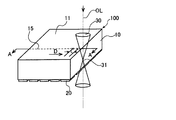
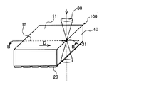
先ず、本発明の発光ダイオードチップの実施形態を説明する。図1は、本発明の一実施形態に係る発光ダイオードチップを支持体に実装したLEDの構造を模式的に示す。なお、倍率は不正確で、実際は、透明基板1の厚さが〜100μmのオーダであるのに対して、発光層を含む半導体膜が積層された半導体層2の厚さは、〜1μmのオーダである。発光ダイオードチップ3は、透明基板1であるサファイア基板の1面11´に、発光層を有する窒化物半導体膜が積層されて半導体層2となり、基板1の2面11は、支持体6(この場合はリードフレームを示している)のカップの底部に接着剤5で接着されている。そして、基板1の1面11´と2面11とに直交するウエハからの分割面12、12′(図示しない紙面に平行な分割面13、13′)には、凹凸が形成されている。なお、4は、窒化物半導体層の正極、及び負極に形成されたオーミック電極であり、このオーミック電極4からワイヤーボンドされて電極がリードフレームと接続されている。
First, an embodiment of a light emitting diode chip of the present invention will be described. FIG. 1 schematically shows the structure of an LED in which a light-emitting diode chip according to an embodiment of the present invention is mounted on a support. In addition, the magnification is inaccurate. Actually, the thickness of the transparent substrate 1 is on the order of .about.100 .mu.m, whereas the thickness of the semiconductor layer 2 on which the semiconductor film including the light emitting layer is laminated is on the order of .about.1 .mu.m. It is. In the light-emitting
透明基板1は、半導体層2の半導体結晶が成長できる基板であればどのような基板でもよく、例えば、サファイア、スピネルのような酸化物系の透明な絶縁体基板の他、酸化亜鉛、窒化ガリウムのような透明な半導体基板も使用可能である。これらの基板は、1面11側に形成された窒化物半導体の発光を透過する。なお、ここでいう透明とは、発光ダイオードの光の大部分(発光光量の80%以上、望ましくは90%以上)を透過可能であることをいう。
The transparent substrate 1 may be any substrate as long as a semiconductor crystal of the semiconductor layer 2 can be grown. For example, in addition to an oxide-based transparent insulator substrate such as sapphire and spinel, zinc oxide and gallium nitride. A transparent semiconductor substrate such as can also be used. These substrates transmit light emitted from the nitride semiconductor formed on the
透明基板1の1面11´に形成される窒化物半導体層2は、例えば、n型GaNコンタクト層+n型AlGaNクラッド層+InGaN活性層+p型AlGaNクラッド層+p型GaN層等を積層したダブルヘテロ構造で形成される。また、この他、p−n接合を有するシングルヘテロ構造、ホモ構造、i層を発光層とするMIS構造等に窒化物半導体が積層されて発光層が形成される。
The nitride semiconductor layer 2 formed on the
透明基板1の分割面12、12′(分割面12、12´と交差する二つの分割面)への凹凸の形成は、ウエットエッチングやフォトリソグラフィ等で行われてもよいが、後述する本発明のウエハ分割加工方法で分割と同時に行われることが望ましい。別途凹凸形成工程を必要とせず、チップ製造コストを下げることができる。
The formation of irregularities on the dividing
透明基板1の2面11と支持体5とを接続する接着剤5は、高分子材料でもよいが、金属を含む導電性材料が望ましい。チップ3の熱を支持体6に効率よく逃がすことができるからである。導電性材料からなる接着剤として、例えば、銀ペーストやInペースト等を用いることができる。
The adhesive 5 that connects the two
支持体6には、多くの種類があり、例えば、リードフレーム、ステム等の金属支持体、アルミナ基板等のセラミック製支持体等を挙げることができる。発光ダイオードチップ3は、これらの支持体上に2面11側が接着剤5を介して載置される。つまりフェースアップと呼ばれる形式で載置される。
There are many types of the
図1に矢印で示すように、本発明のLEDにおいて、透明な窒化物半導体層2からの発光は、同じく透明なサファイア基板1の中を透過して分割面12、12′(分割面12、12´と交差する二つの分割面)に到達する。分割面が鏡面であると、臨界角より大きな入射角の光は、外に出射できないが、凹凸が形成されているため、臨界角より大きな入射角の光も凹凸の切片では臨界角条件をはずれ、外に出射することができる。したがって、光の取り出し効率(外部量子効率)が高くなる。
As shown by the arrows in FIG. 1, in the LED of the present invention, light emitted from the transparent nitride semiconductor layer 2 is transmitted through the transparent sapphire substrate 1 and divided
本発明の発光ダイオードチップは、分割面からの光の取り出し効率が高いので、図1のような所謂フェースアップ形式に限定されることがない。電極4が下向きに支持される所謂フリップチップボンディング形式でも有効に光を取り出すことができる。
The light emitting diode chip of the present invention is not limited to the so-called face-up type as shown in FIG. The so-called flip chip bonding method in which the
次に本発明のウェハ分割加工方法を、例えばサファイア基板に発光層を含む半導体膜が積層され個々の発光素子として機能するようにパターンニングされたウェハからチップに分割する場合について説明する。 Next, the wafer division processing method of the present invention will be described in the case where a semiconductor film including a light emitting layer is stacked on a sapphire substrate and patterned into chips so as to function as individual light emitting elements.
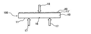
<内部加工工程> 先ず、内部加工工程を図2〜図5と共に説明する。図2で、10がサファイア基板、20がパターニングされた半導体層、半導体層20が積層されていない面11に点線で示す15が分割ラインである。分割ライン15は、半導体層20が積層されている面11´側では、半導体層20の間をとおるように設定されている。図2に示すように、ウェハ100のサファイア基板10によって線形吸収を起こさないような波長を有する、例えば、希土類ドープモードロックファイバレーザベースのフェムト秒レーザ装置から、発生された、例えば、400fsのパルス幅を有する短光パルスレーザビーム5が使用される。この短光パルスレーザビーム5は、ウェハ100のサファイア基板10の半導体層20が積層されていない面11に対して、垂直に且つビーム30のウエスト31が基板1の内部に位置するように集光レンズ200で絞り込まれて入射される。この場合、当該内部加工工程を実施する前に、後述する加工装置(図12)の駆動部で光学ベンチをZ軸方向に微動させ、サファイア基板の面11と集光レンズ200との間隔距離を調整することにより、レーザビーム30のビームウエスト31が基板10の面11から深さ方向に所定の距離入った位置に存在するように設定される。
<Internal Processing Step> First, the internal processing step will be described with reference to FIGS. In FIG. 2, 10 is a sapphire substrate, 20 is a patterned semiconductor layer, and 15 is a
上記集光レンズ200により集光された短光パルスレーザビーム30のウエスト31の面11に垂直な方向(深さ方向)所定位置d0への設定は、先ず、照明光源を用いて上記集光レンズ200の焦点を基板10の面11に設定し、次いで、集光レンズ200を基板10の面11側に所定の距離d移動させることにより行われる。前記所定距離dとd0の関係は、レーザビーム30の波長λと基板10の屈折率n(λ)に依存し、
d0=n(λ)d (1)
と表される。例えば、基板10の厚さが200μmで、面11から深さ方向に80μmの位置にウエスト31を設定する場合、d0=80μm、n(λ)=1.75から、d=45.7μmと求まり、集光レンズ200を面11側に44.4μm移動させればよい。
The setting of the short light
d0 = n (λ) d (1)
It is expressed. For example, when the thickness of the
短光パルスレーザビーム30の光軸OLが、サファイア基板10の面11に想定された分割ライン15(図2中に点線で示す)に沿って、所定の内部加工速度Vinをもって矢印D方向(図2のA−A線から見た一部切欠け断面図である図3においては、紙面に平行方向)に、基板10の面11に対して、相対的に移動させられる。このとき、パルスレーザビーム30の各パルスは、基板10の面11に図2中×印を付して示すように、レーザビーム30のパルス繰り返し周期Rと内部加工移動速度Vinで一義的に定まる間隔Lをもってレーザビーム照射領域であるウエスト領域S、S′(図4参照)に入射する。ここで、間隔Lは
L=Vin/R (2)
と表される。
The optical axis OL of the short optical
It is expressed.
図4は、図3のビームウエスト付近を拡大して模式的に示した図で、実線がある時刻でのパルスによるビームウエスト形状を、点線が次のパルスでのビームウエスト形状を示している。今、図4に示すように、図示しない集光レンズを介して絞り込まれた短光パルスレーザビーム30の一つのパルスがサファイア基板10の内部d0の深さの位置にウエスト領域Sを形成するとする。このウエスト領域Sは、例えば、5TW/cm2(パルス幅400fsとすると、フルーエンス2J/cm2に相当)の高パワー密度の光が照射されると、多光子吸収が惹起され、光誘起破壊域となる。
FIG. 4 is an enlarged view schematically showing the vicinity of the beam waist in FIG. 3. The solid line shows the beam waist shape by a pulse at a certain time, and the dotted line shows the beam waist shape by the next pulse. Now, as shown in FIG. 4, it is assumed that one pulse of the short optical
ビームウエストのスポット径を2W0とすると、レーザビームがシングルモードの場合、
2W0=(4λ/π)(f/2a) (3)
と表される。ここで、fは集光レンズ200の焦点距離、2aは集光レンズに入射するレーザビーム30のビーム径である。
If the spot diameter of the beam waist is 2W 0 , when the laser beam is in single mode,
2W 0 = (4λ / π) (f / 2a) (3)
It is expressed. Here, f is the focal length of the
上記所定の内部加工移動速度Vinは、隣り合うウエストのスポット或いはウエスト領域S、S′が空間的に分離するように定められる。そのためには、L>2W0を満たす必要があり、(2)式から、Vin>2W0Rにすればよいことがわかる。 The predetermined internal machining movement speed Vin is determined such that adjacent waist spots or waist regions S and S ′ are spatially separated. For that purpose, it is necessary to satisfy L> 2W 0, and it is understood from the formula (2) that Vin> 2W 0 R is satisfied.
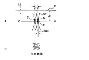
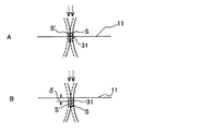
今、Vin>2W0Rとすることで、図4Aに示すようにウエスト領域S、S′が分離したとすると、後述するように分割ライン15にくさびを押し当てて分割すると、図4Aに示す断面が現れる。図4AのC−C断面では、図4Bに示すように光誘起破壊域S、S′が凹になり、SとS′の間が凸になる。図4は、二つのパルスでの光誘起破壊域S、S′しか示していないが、短光パルスレーザビーム30の光軸OLが、分割ライン15に沿って、内部加工速度Vinをもって矢印D方向に、相対的に移動させられるので、順次光誘起破壊域が形成される。すなわち、光誘起破壊域(S、S′)が横方向に繰り返される。
Now, assuming that Vin> 2W 0 R, the waist regions S and S ′ are separated as shown in FIG. 4A. As shown in FIG. A cross section appears. In the CC cross section of FIG. 4A, as shown in FIG. 4B, the light-induced breakdown areas S and S ′ are concave and the space between S and S ′ is convex. FIG. 4 shows only the light-induced breakdown regions S and S ′ with two pulses, but the optical axis OL of the short optical
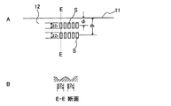
ビームウエスト31を面11から内部深さ方向d0の位置に設定して内部加工を行う上記内部加工工程1の後、ビームウエスト31をd1(<d0)の位置に設定して、内部加工工程2を行うことが好ましい。ウエスト領域Sが分割面12に2段に形成される(図5A参照。)。したがって、分割面の凹凸領域が増えるので、それだけ分割面からの光取り出し効率を高めることができる。なお、後述の実施例では、順次ビームウエスト位置を上(面11側)に上げて内部加工工程19まで行っている。図5bは、図5AのE−E断面図であるが、ウエスト領域を2段形成すると、厚み方向にも凹凸ができる。凹の幅は、ほぼウエスト領域Sの厚み方向の幅2Zrに等しい。ここでZrは、例えば、レーリーレンジとすると、シングルモードのレーザビーム(ガウスビーム)を集光レンズで集光したときのビーム径がウエスト31でのスポット径の√2倍以内である距離である。レーリーレンジZrは
Zr=(4λ/π)(1/2a)2 (4)
と表される。ここで、例えば、波長λ=1.045μmのレーザビームを集光する場合、NA=0.65のとき、f=4mm、2a=3mmを代入すると、Zr=2.4μm、となる。また、NA=0.24のとき、f=20mm、2a=3mmを代入すると、Zr=59μmとなる。したがって、NAが大きいほどZrが小さく、反対にNAが小さいほどZrが大きくなることがわかる。発明者等の実験によれば、NAが0.3以上のとき分割面からの光取り出し効率の観点で好ましいことがわかった。NAが0.4以上がさらに望ましい。なお、後述の溝加工工程を先に行い、その後内部加工工程を行う場合は、NA=0.5以上が好ましい。面11の表層部に溝が加工されていても、その溝を挟んで内部にレーザビームを効率よく集光することができる。NAが大きいと、集光ビームの溝でのケラレが少なくなるからである。
After the internal machining step 1 in which the
It is expressed. Here, for example, when condensing a laser beam having a wavelength λ = 1.45 μm, when NA = 0.65, if f = 4 mm and 2a = 3 mm are substituted, Zr = 2.4 μm. When NA = 0.24, if f = 20 mm and 2a = 3 mm are substituted, Zr = 59 μm. Therefore, it can be seen that the larger NA is, the smaller Zr is, and the smaller NA is, the larger Zr is. According to the experiments by the inventors, it was found that when NA is 0.3 or more, it is preferable from the viewpoint of light extraction efficiency from the divided surface. NA is more preferably 0.4 or more. In addition, when performing the groove | channel processing process mentioned later first and performing an internal processing process after that, NA = 0.5 or more is preferable. Even if a groove is processed in the surface layer portion of the
<溝加工工程> 次に、溝加工工程を図6〜8と共に説明する。図6、8で、10がサファイア基板、20がパターニングされた半導体層である。図6で半導体層20が積層されていない面11に点線で示す15が分割ラインである。分割ライン20は、半導体層20が積層されている面11´側では、半導体層20の間をとおるように設定されている。この場合、当該溝加工工程を実施する前に、後述する加工装置(図12)の駆動部で光学ベンチをZ軸方向に微動させ、サファイア基板の面11と集光レンズ200との間隔距離を調整することにより、レーザビーム5のビームウエスト31が基板10の面11或いはその近辺の表層部(図7Bに示すように、面11から深さ方向に所定距離δ下がった位置)に存在するように設定される。
<Groove Processing Step> Next, the groove processing step will be described with reference to FIGS. 6 and 8, 10 is a sapphire substrate, and 20 is a patterned semiconductor layer. In FIG. 6,
上記集光レンズ200により集光された短光パルスレーザビーム30のウエスト31の面11への設定は、照明光源を用いて上記集光レンズ200の焦点を基板10の面11に設定することで行われる。また、上記集光レンズ200により集光された短光パルスレーザビーム30のウエスト31の面11に垂直な方向(深さ方向)δ下がった位置への設定は、集光レンズ200を基板10の面11側に所定の距離d移動させることにより行われる。このdは(1)式でd0=δとして求められる。
The short
短光パルスレーザビーム30の光軸OLが、サファイア基板10の面11に想定された分割ライン15(図2中に点線で示す)に沿って、所定の溝加工速度Vmをもって矢印D方向(図6のB−B線から見た一部切欠け断面図である図7においては、紙面に平行方向)に、基板10の面11に対して、相対的に移動させられる。このとき、パルスレーザビーム30の各パルスは、レーザビーム30の隣合うパルスのスポットが接する(基板10の面11に図6中○印を付して示すように、)か或いは一部重なるように溝加工移動速度Vmを設定する。
The optical axis OL of the short optical
上記所定の溝加工移動速度Vmは、隣り合うウエスト領域S、S′が空間的に接するか或いは一部重なるように定められる。そのためには、Vm≦2W0Rにすればよい。Vm=2W0Rのときが図7のようにSとS′が接する場合、Vm<2W0RのときがSとS′が重なる場合である。 The predetermined grooving movement speed Vm is determined such that adjacent waist regions S and S ′ are in spatial contact or partially overlap. For this purpose, Vm ≦ 2W 0 R may be set. When Vm = 2W 0 R, S and S ′ are in contact as shown in FIG. 7, and when Vm <2W 0 R, S and S ′ overlap.
図7は、ビームウエスト付近を拡大して模式的に示した図で、実線がある時刻でのパルスによるビームウエスト形状を、点線が次のパルスでのビームウエスト形状を示している。今、図7に示すように、図示しない集光レンズを介して絞り込まれた短光パルスレーザビーム30の一つのパルスがサファイア基板10の面11或いはその近辺の表層部のδの深さの位置にウエスト領域Sを形成するとする。このウエスト領域Sは、例えば、5TW/cm2(パルス幅400fsとすると、フルーエンス2J/cm2に相当)の高パワー密度の光が照射されると、多光子吸収が惹起され、光誘起破壊域となる。
FIG. 7 is an enlarged view schematically showing the vicinity of the beam waist. The solid line shows the beam waist shape by a pulse at a certain time, and the dotted line shows the beam waist shape by the next pulse. Now, as shown in FIG. 7, one pulse of the short optical
今、例えば、Vm=2W0Rとすることで、図7に示すようにウエスト領域S、S′が接し、図8に示すように加工域が連続した溝16が形成される。なお、この溝加工工程での光誘起破壊域からは蒸気や粒子が外部に噴出されるが、この面11には半導体層20が積層されていないので、所謂デブリが問題にならない。
Now, for example, by setting Vm = 2W 0 R, the waist regions S and S ′ are in contact with each other as shown in FIG. 7, and a
なお、後述の実施例では、図7Aに示すように、最初ビームウエストを基板10の面11に設定して溝加工を行った後、ビームウエストを面11から3μm下がった位置に設定して、さらに溝加工を行い、溝の深さを深くしている。こうすることで、より確実に分割することができる。
In the embodiment described later, as shown in FIG. 7A, after the first beam waist is set on the
<分割加工工程> 次に、上記内部加工工程で分割ラインに沿って形成されたサファイア基板30の内部光誘起破壊域と、上記溝加工工程で当該分割ラインに沿って形成された基板10の面11に形成された溝とを介して分割又は割断する工程について図9と共に説明する。 図9で、10がサファイア基板、20がパターニングされた半導体層、16が分割ラインに沿って形成された溝である。まず、図9に示すように、上述した内部加工及び表面溝加工されたウエハ100の分割ラインに沿って形成された溝16の両側部(図9中白抜き矢印17で示す部分)を保持又は固定する一方、基板10の他面11′における上記溝16に対応する部分(図9中、白抜き矢印18で示す部分)に図示しないブレーク刃等の刃先を押し当てて押圧することにより、溝16に歪み応力を集中作用させ、上記ウエハ100を分割ラインに沿って簡単且つ容易に分割又は割断することができる。
<Division processing step> Next, the internal light-induced breakdown region of the
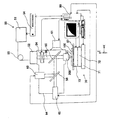
次に本発明の分割加工方法を実施する分割加工装置を図12と共に説明する。分割加工装置は、レーザビーム30を発生するレーザ装置50と、レーザビーム30をON−OFF制御するシャッター54と、レーザビーム30を透過するダイクロイックミラー55と、ダイクロイックミラー55を透過したレーザビーム30を集光する集光レンズ200と、集光レンズ200で集光されたレーザビーム30がZ軸方向から入射される加工対象物のウエハ100が載置される載置台57と、載置台57をX軸方向に移動させるためのX軸ステージ71と、載置台57をX軸方向に直交するY軸方向に移動させるためのY軸ステージ72と、載置台57をX軸及びY軸方向に直交するZ軸方向に移動させるためのZ軸ステージ73と、制御用パソコン80と、を備える。
Next, a division processing apparatus for carrying out the division processing method of the present invention will be described with reference to FIG. The division processing apparatus includes a
分割加工装置は、さらに、載置台57に載置されたウエハ100を可視光線で照明して観察するための可視光線を発生する観察光源63と、観察光源63からの可視光線を90°曲げてダイクロイックミラー55に入射させるハーフミラー56と、集光レンズ200、ダイクロイックミラー55、及びハーフミラー56を介してウエハ100を撮像するCCDカメラ62を備える。
The division processing apparatus further includes an
分割加工装置はさらに、レーザ装置50、シャッター54、ダイクロイックミラー55、集光レンズ200、ハーフミラー56、観察光源63、及びCCDカメラ62を配置する光学ベンチ64と、光学ベンチ64をZ軸方向に駆動する駆動部61と、を備える。
The split processing apparatus further includes an
シャッター54、観察光源63、CCDカメラ62、及び駆動部61は制御用パソコン80に接続されており、シャッター54、観察光源63のON−OFF制御、CCDカメラ62の撮像データ処理、駆動部61の駆動制御が行われる。したがって、制御用パソコン80からの命令でレーザビーム30のウエスト位置(焦点位置)31をCCDカメラ62で撮像して制御用パソコン80のモニター上で観察することができる。
The
レーザ装置50は、発振モジュール51と、発振モジュール51から発振されたレーザ光を伝播するファイバ53と、ファイバ53を伝播してきたレーザ光を増幅する増幅モジュール52と、発振モジュール51からのレーザ光の出力、パルス幅、繰返し周波数を制御するレーザコントローラ54と、を備える。レーザコントローラ54はパソコン80に接続されており、パソコン80からの命令で動作する。発振モジュール51は、Er、Yb共ドープのモードロックファイバレーザと、ファイバレーザから発振されたパルスレーザ光を受光して伸張されたパルスレーザ光を出力するファイバー伸張器と、伸張されたパルスレーザ光を受光してパルスを間引くパルス間引き器と、伸張されて間引かれたパルスレーザ光を受光して増幅されたパルスレーザ光を出力するファイバー前置増幅器と、を備える。増幅モジュール52は、発振モジュール51からのパルスレーザ光をファイバ53を通して受光してさらに増幅するファイバ主増幅器と、増幅されたパルスレーザ光を受光して圧縮されたパルスレーザ光を出力する圧縮器と、を備える。増幅モジュール52は光学ベンチ64にレーザビーム30がZ軸方向に出射されるように固定されている。増幅モジュール52からは波長が1045nm、平均出力が250mW、パルス幅が400〜600fs、繰り返し周波数が50〜200kHzのレーザビームLが出射される。
The
レーザ装置50は、上記の他に、波長が300〜1800nm、パルス幅が10fs〜10ps、繰り返し周波数が50kHz〜10MHzの性能を有するものであればよい。例えば、再生増幅タイプのTi:サファイアレーザ装置等を用いてもよい。レーザ装置50は、波長が700〜1600nm、パルス幅が50fs〜2ps、繰り返し周波数が50〜300kHzのレーザビームを出力することが望ましい。この性能のレーザビームを用いると、分割面に形成される凹凸での光吸収が少なく、分割面からの光の取り出し効率をさらに高めることができるからである。
In addition to the above, the
以下に、上記構成の分割加工装置の操作手順について説明する。まず、シャッター54を閉じ、レーザ装置50を所定の繰り返し周波数で運転する。次にシャッター54を開いて集光レンズ200を出射するレーザビーム30のパルスエネルギが所定の値になるようにコントローラ54で発振モジュール51を制御する。
Hereinafter, an operation procedure of the division processing apparatus having the above configuration will be described. First, the
次に、シャッター54を閉じて、載置台57に分割ライン15の方向がX軸方向になるようにウエハ100をセットする。次に、観察光源63をONしてCCDカメラ62でウエハ100の表面11を観察しながら、焦点位置が表面11の分割ライン15に一致するようにX軸ステージ71、Y軸ステージ72を移動させると共に、駆動部61で光学ベンチ64をZ軸方向に微動させる。
Next, the
次に、ウエスト位置31が表面11から所定の深さd0に位置するように、駆動部61で光学ベンチ64を表面11に近づける(下降させる)。
Next, the
次に、シャッター54をONしてレーザビーム30をウエスト位置に集光照射しながらウエハ100をX軸ステージ71でX軸方向に所定の移動速度Vinで移動させ、所定の距離移動させたらシャッター54をOFFする。
Next, when the
次に、ウエスト位置31が表面11から所定の深さd1(<d0)に位置するように、駆動部61で光学ベンチ64を表面11から遠ざける(上昇させる)。
Next, the
次に、シャッター54をONしてレーザビーム30をウエスト位置に集光照射しながらウエハ100をX軸ステージ71でX軸方向に所定の移動速度Vinで移動させ、所定の距離移動させたらシャッター54をOFFする。
Next, when the
次に、ウエスト位置31が表面11に位置するように、駆動部61で光学ベンチ64を表面11から遠ざける(上昇させる)。
Next, the
次に、シャッター54をONしてレーザビーム30をウエスト位置に集光照射しながらウエハ100をX軸ステージ71でX軸方向に所定の移動速度Vmで移動させ、所定の距離移動させたらシャッター54をOFFする。
Next, when the
図10に示すように、内部加工を1段から順に19段まで行い、その後溝加工を20段、21段行った。 As shown in FIG. 10, the internal machining was performed from the first to the 19th in order, and then the grooving was performed in the 20th and 21st stages.
加工条件
加工対象:サファイア単結晶(厚みt=500μm)
レーザ装置:Er、Yb共ドープモードロックファイバレーザベースフェムト秒レーザ装置
波長:1.045μm
パルス幅:400fs
パルス繰り返し周波数:100kHz
集光レンズ:開口数0.65、焦点距離4mm
集光レンズ透過後のパルスエネルギ:1.5μJ
ビームウエストでのフルーエンス:160J/cm2(計算値)
ビームウエストのパワー密度:400TW/cm2(計算値)
レーザビーム入射面:サファイア結晶のC面(図10の11)
レーザビーム入射方向:C面に垂直(図10に白抜き矢印で示す方向)
内部加工段数:19段(図10の1段〜19段)
1段目のウエスト位置:入射面から厚み方向内部に469μm(集光レンズの焦点位置を入射面に合わせてから集光レンズを入射面に268μm近づけたときの計算値)入った位置
内部加工段間の間隔:24.5μm(前段の内部加工後に集光レンズを入射面から14μm遠ざけたときの計算値)
内部加工移動速度Vin:400mm/s
溝加工段数:2段(図10の20段、21段)
20段目のウエスト位置:入射面
21断面のウエスト位置:集光レンズの焦点位置を入射面に合わせてから集光レンズを入射面に3μm近づけた位置
溝加工移動速度Vm:200mm/s
Processing conditions Processing object: Sapphire single crystal (thickness t = 500 μm)
Laser device: Er, Yb co-doped mode-locked fiber laser-based femtosecond laser device Wavelength: 1.045 μm
Pulse width: 400 fs
Pulse repetition frequency: 100 kHz
Condensing lens: numerical aperture 0.65,
Pulse energy after passing through the condenser lens: 1.5 μJ
Fluence at the beam waist: 160 J / cm 2 (calculated value)
Beam waist power density: 400 TW / cm 2 (calculated value)
Laser beam incident surface: C-plane of sapphire crystal (11 in FIG. 10)
Laser beam incident direction: perpendicular to C-plane (direction indicated by white arrow in FIG. 10)
Number of internal machining steps: 19 (1 to 19 in FIG. 10)
First stage waist position: Position internal processing stage containing 469 μm inside the thickness direction from the incident surface (calculated value when the condensing lens is brought close to the incident surface after adjusting the focal point of the condensing lens to the incident surface) Interval: 24.5 μm (calculated value when the condenser lens is moved 14 μm away from the incident surface after the internal processing in the previous stage)
Internal processing moving speed Vin: 400mm / s
Number of grooving steps: 2 steps (20 steps and 21 steps in FIG. 10)
Waist position of 20th stage: Waist position of cross section of incident surface 21: Position groove processing moving speed Vm: 200 mm / s when the condensing lens is brought close to the incident surface after adjusting the focal position of the condensing lens to the incident surface
サファイア基板の分割加工結果を図11に示す。これは、上記加工条件で内部加工と溝加工を行った後、ブレーク刃の刃先を押し当てて押圧して分割した分割面の顕微鏡写真である。厚み方向に細長い白っぽく見える部分が光誘起破壊域で、非加工領域(黒っぽく見える部分)を挟んで分離して配列している。この白っぽく見える部分が紙面方向(分割面と直交する方向)に凹んでいて、その凹みの深さは約1μmであった。また、移動方向の凹みのピッチは4〜5μmであった。 FIG. 11 shows the result of dividing the sapphire substrate. This is a micrograph of a divided surface obtained by performing internal machining and grooving under the above machining conditions, and then pressing and pressing the edge of a break blade. The portions that appear whitish in the thickness direction are light-induced destruction regions, which are arranged separately with a non-processed region (a portion that appears blackish) in between. This whitish portion was recessed in the paper surface direction (direction orthogonal to the dividing surface), and the depth of the recess was about 1 μm. Moreover, the pitch of the dents in the moving direction was 4 to 5 μm.
次に、この分割面からの光取り出し効率を測定した。11面及び11´面を除く4面のうち測定面以外の3面を鏡面研磨し、11´面に表面実装型の青色LEDを屈折率1.55のUV硬化接着剤で接着した。そして、測定面から出射される光量を測定して、光取り出し効率が6%向上することを確認した。 Next, the light extraction efficiency from this divided surface was measured. Of the four surfaces excluding the 11th and 11 ′ surfaces, 3 surfaces other than the measurement surface were mirror-polished, and a surface-mounted blue LED was adhered to the 11 ′ surface with a UV curable adhesive having a refractive index of 1.55. And the light quantity radiate | emitted from a measurement surface was measured, and it confirmed that light extraction efficiency improved 6%.
発光ダイオード、特に高輝度発光ダイオード産業に利用される可能性が極めて高い。 It is very likely to be used in light emitting diodes, especially in the high-intensity light emitting diode industry.
1、10・・・・・・透明基板(サファイア基板)
2、20・・・・・・半導体膜(半導体層)
11・・・・・・・・入射面
12・・・・・・・・分割面
15・・・・・・・・分割ライン
30・・・・・・・・レーザビーム
31・・・・・・・・ウエスト
100・・・・・・・ウエハ
200・・・・・・・集光レンズ
CL・・・・・・・・光軸
S、S′・・・・・・ウエスト領域
1, 10 ... Transparent substrate (sapphire substrate)
2, 20 .... Semiconductor film (semiconductor layer)
11...
Claims (4)
希土類ドープモードロックファイバレーザベースのフェムト秒レーザ装置によって、前記ウェハに対し光学的に透明な波長を有する、パルス幅がフェムト秒オーダの繰り返し短光パルスレーザビームを集光レンズを介して該ウェハの他方の面を入射面として入射させ、前記レーザビームのウエストが前記ウェハの内部に存在するように前記集光レンズの焦点位置を調整し、該レーザビームの光軸を該ウェハに対して想定された分割ラインに沿って該ウエストのスポットが空間的に分離するように該ウェハに対して相対的に移動させながら、該ウェハの該入射面に該レーザビームを入射する毎に、該ウエストの領域に多光子吸収による光誘起破壊を起こさせる第1の内部加工工程と、
前記レーザビームのウエストが前記ウェハの前記入射面の表層部に存在するように前記集光レンズの焦点位置を調整し、該レーザビームの光軸を前記分割ラインに沿って該ウエストのスポットが空間的に繋がるか或いは重なるように該ウェハに対して相対的に移動させながら、該ウェハの該入射面に該レーザビームを入射する毎に、該ウエストの領域に多光子吸収による光誘起破壊を起こさせて溝を形成する溝加工工程と、
前記溝に沿って前記ウェハを分割する分割加工工程と
を含み、
前記発光ダイオードチップのチップ分割面に凹凸が形成されることを特徴とするウェハ分割加工方法。 A wafer division processing method for producing a light emitting diode chip by dividing a wafer in which a semiconductor film including a light emitting layer is laminated on one surface of a transparent substrate having two opposite surfaces,
By means of a rare earth doped mode-locked fiber laser-based femtosecond laser device, a repeated short optical pulse laser beam having a wavelength optically transparent to the wafer and having a pulse width on the order of femtoseconds is passed through the condenser lens. The other surface is used as an incident surface, the focal position of the condensing lens is adjusted so that the waist of the laser beam exists inside the wafer, and the optical axis of the laser beam is assumed with respect to the wafer. Each time the laser beam is incident on the incident surface of the wafer, the waist region is moved relative to the wafer so that the waist spot is spatially separated along the dividing line. A first internal processing step for causing light-induced breakdown due to multiphoton absorption;
The focal position of the condenser lens is adjusted so that the waist of the laser beam exists on the surface layer portion of the incident surface of the wafer, and the spot of the waist is spaced along the dividing line with the optical axis of the laser beam. Each time the laser beam is incident on the incident surface of the wafer while moving relative to the wafer so as to be connected or overlapped with each other, light-induced destruction due to multiphoton absorption occurs in the waist region. A groove processing step for forming grooves,
A dividing step of dividing the wafer along the groove,
A method of dividing a wafer, wherein irregularities are formed on a chip dividing surface of the light emitting diode chip.
Priority Applications (4)
| Application Number | Priority Date | Filing Date | Title |
|---|---|---|---|
| JP2006152023A JP5221007B2 (en) | 2006-05-31 | 2006-05-31 | Light emitting diode chip and wafer split processing method |
| US11/806,068 US20070298529A1 (en) | 2006-05-31 | 2007-05-29 | Semiconductor light-emitting device and method for separating semiconductor light-emitting devices |
| CNB2007101058387A CN100568565C (en) | 2006-05-31 | 2007-05-30 | Light emitting semiconductor device and the method that is used for the separating semiconductor luminescent device |
| TW096119474A TW200805718A (en) | 2006-05-31 | 2007-05-31 | Semiconductor light-emitting device and method for separating semiconductor light-emitting devices |
Applications Claiming Priority (1)
| Application Number | Priority Date | Filing Date | Title |
|---|---|---|---|
| JP2006152023A JP5221007B2 (en) | 2006-05-31 | 2006-05-31 | Light emitting diode chip and wafer split processing method |
Publications (2)
| Publication Number | Publication Date |
|---|---|
| JP2007324326A JP2007324326A (en) | 2007-12-13 |
| JP5221007B2 true JP5221007B2 (en) | 2013-06-26 |
Family
ID=38856858
Family Applications (1)
| Application Number | Title | Priority Date | Filing Date |
|---|---|---|---|
| JP2006152023A Active JP5221007B2 (en) | 2006-05-31 | 2006-05-31 | Light emitting diode chip and wafer split processing method |
Country Status (2)
| Country | Link |
|---|---|
| JP (1) | JP5221007B2 (en) |
| CN (1) | CN100568565C (en) |
Cited By (2)
| Publication number | Priority date | Publication date | Assignee | Title |
|---|---|---|---|---|
| US9583674B2 (en) | 2014-06-18 | 2017-02-28 | Nichia Corporation | Method for producing semiconductor light emitting element |
| US9873170B2 (en) | 2015-03-24 | 2018-01-23 | Nichia Corporation | Method of manufacturing light emitting element |
Families Citing this family (39)
| Publication number | Priority date | Publication date | Assignee | Title |
|---|---|---|---|---|
| US9138913B2 (en) * | 2005-09-08 | 2015-09-22 | Imra America, Inc. | Transparent material processing with an ultrashort pulse laser |
| DE102006042280A1 (en) | 2005-09-08 | 2007-06-06 | IMRA America, Inc., Ann Arbor | Transparent material scribing comprises using single scan of focused beam of ultrashort laser pulses to simultaneously create surface groove in material and modified region(s) within bulk of material |
| BR122019015544B1 (en) | 2009-02-25 | 2020-12-22 | Nichia Corporation | method for making a semiconductor element, and, semiconductor element |
| US8216867B2 (en) * | 2009-06-10 | 2012-07-10 | Cree, Inc. | Front end scribing of light emitting diode (LED) wafers and resulting devices |
| JP2011161491A (en) * | 2010-02-10 | 2011-08-25 | Disco Abrasive Syst Ltd | Laser beam machining apparatus |
| JP5513227B2 (en) * | 2010-04-08 | 2014-06-04 | 株式会社フジクラ | Fine structure forming method, laser irradiation apparatus, and substrate |
| JP5981094B2 (en) * | 2010-06-24 | 2016-08-31 | 東芝機械株式会社 | Dicing method |
| CN101908505B (en) * | 2010-06-24 | 2013-04-24 | 上海蓝光科技有限公司 | Method for manufacturing light-emitting diode chip |
| US8735772B2 (en) * | 2011-02-20 | 2014-05-27 | Electro Scientific Industries, Inc. | Method and apparatus for improved laser scribing of opto-electric devices |
| EP2721654B1 (en) * | 2011-06-15 | 2016-11-16 | Seoul Viosys Co., Ltd. | Semiconductor light emitting device and method of manufacturing the same |
| JP2013042119A (en) * | 2011-07-21 | 2013-02-28 | Hamamatsu Photonics Kk | Light-emitting element manufacturing method |
| CN103050584B (en) * | 2011-10-17 | 2015-05-20 | 上海蓝光科技有限公司 | Method for preparing light-emitting diode chip |
| JP6000700B2 (en) * | 2012-07-10 | 2016-10-05 | 株式会社ディスコ | Laser processing method |
| CN102886609A (en) * | 2012-08-27 | 2013-01-23 | 中国科学院半导体研究所 | Multi-focus femtosecond laser scribing method applied to separation of light emitting diode (LED) device |
| CN105189024B (en) * | 2013-04-04 | 2018-01-30 | Lpkf激光电子股份公司 | Method and apparatus for separating base plate |
| EP2964417B1 (en) * | 2013-04-04 | 2022-01-12 | LPKF Laser & Electronics AG | Method for providing through-openings in a substrate |
| US20150034613A1 (en) * | 2013-08-02 | 2015-02-05 | Rofin-Sinar Technologies Inc. | System for performing laser filamentation within transparent materials |
| JP6255192B2 (en) * | 2013-09-04 | 2017-12-27 | 株式会社ディスコ | Optical device and processing method of optical device |
| CN103586588B (en) * | 2013-11-26 | 2015-07-29 | 苏州光韵达光电科技有限公司 | The fiber laser device of cutting sapphire glass and cutting method |
| JP6277017B2 (en) * | 2014-03-03 | 2018-02-07 | 株式会社ディスコ | Optical device |
| CN111430511A (en) * | 2014-07-25 | 2020-07-17 | 晶元光电股份有限公司 | Light emitting element and method for manufacturing the same |
| CN105990482A (en) * | 2015-03-19 | 2016-10-05 | 晶元光电股份有限公司 | Light emitting device and method of fabricating the same |
| JP6548944B2 (en) * | 2015-04-09 | 2019-07-24 | 株式会社ディスコ | Laser processing equipment |
| JPWO2017208535A1 (en) * | 2016-06-03 | 2019-03-28 | 創光科学株式会社 | Nitride semiconductor ultraviolet light emitting device and method of manufacturing the same |
| CN107243690A (en) * | 2017-07-13 | 2017-10-13 | 华中科技大学 | A kind of laser multifocal dynamic machining method and system |
| CN107538136A (en) * | 2017-07-31 | 2018-01-05 | 山东浪潮华光光电子股份有限公司 | It is a kind of to utilize the method for being cut by laser sapphire substrate LED chip |
| JP7007052B2 (en) * | 2017-09-19 | 2022-01-24 | 株式会社ディスコ | Wafer processing method |
| JP7105058B2 (en) * | 2017-12-05 | 2022-07-22 | 株式会社ディスコ | Wafer processing method |
| WO2019220666A1 (en) * | 2018-05-17 | 2019-11-21 | 信越エンジニアリング株式会社 | Workpiece separation device and workpiece separation method |
| WO2020210959A1 (en) * | 2019-04-15 | 2020-10-22 | 厦门市三安光电科技有限公司 | Led chiplet and invisible cutting method for led chip |
| CN110216389A (en) * | 2019-07-01 | 2019-09-10 | 大族激光科技产业集团股份有限公司 | A kind of laser processing and system of wafer |
| CN110416155B (en) * | 2019-07-05 | 2021-10-15 | 佛山市国星半导体技术有限公司 | LED wafer cutting and splitting method and LED chip |
| CN110456172A (en) * | 2019-08-05 | 2019-11-15 | 清华大学 | Non-invasive E-field measuring system and method |
| CN111276577B (en) * | 2019-12-18 | 2021-12-10 | 北京中科优唯科技有限公司 | Manufacturing method of LED chip |
| CN112166507B (en) * | 2020-01-06 | 2022-07-22 | 厦门三安光电有限公司 | Manufacturing method of light emitting diode |
| US11592166B2 (en) | 2020-05-12 | 2023-02-28 | Feit Electric Company, Inc. | Light emitting device having improved illumination and manufacturing flexibility |
| US11876042B2 (en) | 2020-08-03 | 2024-01-16 | Feit Electric Company, Inc. | Omnidirectional flexible light emitting device |
| KR102214104B1 (en) * | 2020-12-03 | 2021-02-09 | 주식회사 아성 | Mask frame surface treatment method using laser cleaning |
| CN113394312B (en) * | 2021-06-11 | 2023-03-10 | 湘能华磊光电股份有限公司 | Chip and cutting method thereof |
Family Cites Families (13)
| Publication number | Priority date | Publication date | Assignee | Title |
|---|---|---|---|---|
| DE4305296C3 (en) * | 1993-02-20 | 1999-07-15 | Vishay Semiconductor Gmbh | Method of manufacturing a radiation emitting diode |
| JPH08167738A (en) * | 1994-12-14 | 1996-06-25 | Sanken Electric Co Ltd | Semiconductor light emitting element |
| JP2003188410A (en) * | 2001-12-19 | 2003-07-04 | Daido Steel Co Ltd | Light emitting diode chip |
| JP3715627B2 (en) * | 2002-01-29 | 2005-11-09 | 株式会社東芝 | Semiconductor light emitting device and manufacturing method thereof |
| JP4329374B2 (en) * | 2002-07-29 | 2009-09-09 | パナソニック電工株式会社 | LIGHT EMITTING ELEMENT AND MANUFACTURING METHOD THEREOF |
| JP2004221112A (en) * | 2003-01-09 | 2004-08-05 | Sharp Corp | Oxide semiconductor light emitting element |
| JP2004247411A (en) * | 2003-02-12 | 2004-09-02 | Sharp Corp | Semiconductor light emitting device and its manufacturing method |
| JP4669216B2 (en) * | 2003-11-25 | 2011-04-13 | パナソニック電工株式会社 | Manufacturing method of semiconductor light emitting device |
| JP2005268329A (en) * | 2004-03-16 | 2005-09-29 | Daido Steel Co Ltd | Semiconductor light emitting element |
| JP4092658B2 (en) * | 2004-04-27 | 2008-05-28 | 信越半導体株式会社 | Method for manufacturing light emitting device |
| JP2006245066A (en) * | 2005-02-28 | 2006-09-14 | Seiwa Electric Mfg Co Ltd | Light emitting diode and method of manufacturing light emitting diode |
| JP2006253298A (en) * | 2005-03-09 | 2006-09-21 | Toshiba Corp | Semiconductor light emitting element and device therefor |
| JP2007258672A (en) * | 2006-02-22 | 2007-10-04 | Sharp Corp | Light-emitting diode and its manufacturing method |
-
2006
- 2006-05-31 JP JP2006152023A patent/JP5221007B2/en active Active
-
2007
- 2007-05-30 CN CNB2007101058387A patent/CN100568565C/en not_active Expired - Fee Related
Cited By (3)
| Publication number | Priority date | Publication date | Assignee | Title |
|---|---|---|---|---|
| US9583674B2 (en) | 2014-06-18 | 2017-02-28 | Nichia Corporation | Method for producing semiconductor light emitting element |
| US10340413B2 (en) | 2014-06-18 | 2019-07-02 | Nichia Corporation | Semiconductor light emitting element |
| US9873170B2 (en) | 2015-03-24 | 2018-01-23 | Nichia Corporation | Method of manufacturing light emitting element |
Also Published As
| Publication number | Publication date |
|---|---|
| CN100568565C (en) | 2009-12-09 |
| CN101083292A (en) | 2007-12-05 |
| JP2007324326A (en) | 2007-12-13 |
Similar Documents
| Publication | Publication Date | Title |
|---|---|---|
| JP5221007B2 (en) | Light emitting diode chip and wafer split processing method | |
| US20070298529A1 (en) | Semiconductor light-emitting device and method for separating semiconductor light-emitting devices | |
| JP6260601B2 (en) | Manufacturing method of semiconductor device | |
| TWI631665B (en) | Optical device processing method | |
| TWI433745B (en) | Laser processing method and laser processing apparatus | |
| TWI450784B (en) | Laser processing device | |
| US9117895B2 (en) | Laser processing method | |
| JP6620825B2 (en) | Manufacturing method of semiconductor device | |
| WO2014030519A1 (en) | Workpiece cutting method | |
| US20140014976A1 (en) | Optical device and processing method of the same | |
| KR20140004017A (en) | Laser dicing method | |
| JP6277017B2 (en) | Optical device | |
| TWI623366B (en) | Optical device processing method | |
| TW201529267A (en) | Optical device and manufacturing method therefor | |
| JP2009032970A (en) | Method of manufacturing nitride semiconductor element | |
| JP6318900B2 (en) | Manufacturing method of semiconductor light emitting device | |
| JP2011134955A (en) | Method of producing chip component from plate material | |
| WO2014030517A1 (en) | Workpiece cutting method | |
| KR101889385B1 (en) | Method for processing substrate with pattern | |
| US10297710B2 (en) | Method of processing wafer | |
| KR100984719B1 (en) | Laser processing apparatus | |
| JP2013118413A (en) | Led chip | |
| JP2015162565A (en) | Substrate with led pattern, method for manufacturing the same, and method for manufacturing led element | |
| JP2009032795A (en) | Method of manufacturing nitride semiconductor light emitting element | |
| JP2013118277A (en) | Method for processing substrate with led pattern |
Legal Events
| Date | Code | Title | Description |
|---|---|---|---|
| A521 | Written amendment |
Free format text: JAPANESE INTERMEDIATE CODE: A523 Effective date: 20080410 |
|
| A521 | Written amendment |
Free format text: JAPANESE INTERMEDIATE CODE: A821 Effective date: 20080410 |
|
| A621 | Written request for application examination |
Free format text: JAPANESE INTERMEDIATE CODE: A621 Effective date: 20080929 |
|
| A977 | Report on retrieval |
Free format text: JAPANESE INTERMEDIATE CODE: A971007 Effective date: 20110629 |
|
| A521 | Written amendment |
Free format text: JAPANESE INTERMEDIATE CODE: A523 Effective date: 20110907 |
|
| RD03 | Notification of appointment of power of attorney |
Free format text: JAPANESE INTERMEDIATE CODE: A7423 Effective date: 20110907 |
|
| RD04 | Notification of resignation of power of attorney |
Free format text: JAPANESE INTERMEDIATE CODE: A7424 Effective date: 20110907 |
|
| A521 | Written amendment |
Free format text: JAPANESE INTERMEDIATE CODE: A821 Effective date: 20110909 |
|
| A131 | Notification of reasons for refusal |
Free format text: JAPANESE INTERMEDIATE CODE: A131 Effective date: 20111102 |
|
| A521 | Written amendment |
Free format text: JAPANESE INTERMEDIATE CODE: A523 Effective date: 20111221 |
|
| A02 | Decision of refusal |
Free format text: JAPANESE INTERMEDIATE CODE: A02 Effective date: 20120823 |
|
| A521 | Written amendment |
Free format text: JAPANESE INTERMEDIATE CODE: A523 Effective date: 20121113 |
|
| A911 | Transfer to examiner for re-examination before appeal (zenchi) |
Free format text: JAPANESE INTERMEDIATE CODE: A911 Effective date: 20121120 |
|
| TRDD | Decision of grant or rejection written | ||
| A01 | Written decision to grant a patent or to grant a registration (utility model) |
Free format text: JAPANESE INTERMEDIATE CODE: A01 Effective date: 20130212 |
|
| A61 | First payment of annual fees (during grant procedure) |
Free format text: JAPANESE INTERMEDIATE CODE: A61 Effective date: 20130307 |
|
| FPAY | Renewal fee payment (event date is renewal date of database) |
Free format text: PAYMENT UNTIL: 20160315 Year of fee payment: 3 |
|
| R150 | Certificate of patent or registration of utility model |
Ref document number: 5221007 Country of ref document: JP Free format text: JAPANESE INTERMEDIATE CODE: R150 Free format text: JAPANESE INTERMEDIATE CODE: R150 |
|
| R250 | Receipt of annual fees |
Free format text: JAPANESE INTERMEDIATE CODE: R250 |
|
| R250 | Receipt of annual fees |
Free format text: JAPANESE INTERMEDIATE CODE: R250 |
|
| R250 | Receipt of annual fees |
Free format text: JAPANESE INTERMEDIATE CODE: R250 |
|
| R250 | Receipt of annual fees |
Free format text: JAPANESE INTERMEDIATE CODE: R250 |
|
| R250 | Receipt of annual fees |
Free format text: JAPANESE INTERMEDIATE CODE: R250 |
|
| R250 | Receipt of annual fees |
Free format text: JAPANESE INTERMEDIATE CODE: R250 |