JP5153089B2 - Inspection method of semiconductor integrated circuit - Google Patents
Inspection method of semiconductor integrated circuit Download PDFInfo
- Publication number
- JP5153089B2 JP5153089B2 JP2006151862A JP2006151862A JP5153089B2 JP 5153089 B2 JP5153089 B2 JP 5153089B2 JP 2006151862 A JP2006151862 A JP 2006151862A JP 2006151862 A JP2006151862 A JP 2006151862A JP 5153089 B2 JP5153089 B2 JP 5153089B2
- Authority
- JP
- Japan
- Prior art keywords
- wiring
- circuit
- test pad
- test
- current
- Prior art date
- Legal status (The legal status is an assumption and is not a legal conclusion. Google has not performed a legal analysis and makes no representation as to the accuracy of the status listed.)
- Expired - Fee Related
Links
Images


Landscapes
- Semiconductor Integrated Circuits (AREA)
- Design And Manufacture Of Integrated Circuits (AREA)
Description
本発明は、半導体装置の回路試験を行うスタンダードセルの構成に関する。 The present invention relates to a configuration of a standard cell for performing a circuit test of a semiconductor device.
近年、様々な電子機器において多機能化が求められている。それに伴い、電子機器を動作させる回路にはより多くの機能が求められ、回路の規模が大きくなっている。従来、大規模な回路を容易に作製するために、機能別にセル(スタンダードセル)を作り分け、個々のセルを自動レイアウトによって配置し、セル間を配線で接続する方法が用いられている。例えば、NAND回路、フリップフロップ回路、バーファー回路等をそれぞれスタンダードセルとし、自動配置配線ツールを用いてそれぞれのスタンダードセルを適当な位置に配置し、それぞれを配線で接続することにより大規模な回路を作製する。 In recent years, various electronic devices have been required to have multiple functions. Accordingly, more functions are required for a circuit that operates an electronic device, and the scale of the circuit is increased. Conventionally, in order to easily produce a large-scale circuit, a method is used in which cells (standard cells) are separately formed according to function, individual cells are arranged by automatic layout, and the cells are connected by wiring. For example, NAND circuits, flip-flop circuits, buffer circuits, etc. are standard cells, and each standard cell is placed at an appropriate position using an automatic placement and routing tool. Make it.
回路の規模が大きくなるにつれて、回路内で不良箇所の発生する割合も高くなるため、精度良く容易に不良箇所を検出する方法が求められている。そこで、回路の不良検査方法として、例えば、電圧検出用のパッドを含むスタンダードセルを自動配置することにより、回路上の任意のノード電位の検出をより容易に行う方法が提案されている(特許文献1)。 As the scale of the circuit increases, the rate of occurrence of defective portions in the circuit also increases, so a method for easily detecting defective portions with high accuracy is required. Therefore, as a circuit defect inspection method, for example, a method for easily detecting an arbitrary node potential on a circuit by automatically arranging standard cells including a voltage detection pad is proposed (Patent Document). 1).
しかしながら、回路の不良検査を行うにあたり、電圧だけでなく電流を測定する必要がある。回路内に電流のリーク箇所がある場合、回路の信頼性に影響を与える可能性がある。また、リークなどの原因で回路に必要以上に大きな電流が流れる場合には、回路の発熱や損傷、消費電力の増加等が生じる可能性がある。よって、回路内の消費電流の多い領域あるいは配線を特定し、回路の修正を行う必要がある。特に、RFIDチップ開発においては、消費電力が通信距離に関係するため、電流の流れを細かく検出して、消費電流の多い箇所(不良箇所)を発見して消費電力を抑える必要がある。 However, it is necessary to measure not only the voltage but also the current when performing a circuit defect inspection. If there is a current leak point in the circuit, the reliability of the circuit may be affected. In addition, when a current larger than necessary flows in the circuit due to a leak or the like, there is a possibility that the circuit is heated or damaged, power consumption is increased, or the like. Therefore, it is necessary to specify a region or wiring having a large current consumption in the circuit and correct the circuit. Particularly in the development of an RFID chip, since power consumption is related to the communication distance, it is necessary to detect a current flow in detail, find a portion with a large current consumption (defective portion), and suppress power consumption.
そこで、半導体装置の回路上の特定のノードの電流を測定する方法として、レイアウトの配線領域のうち配線等がない空き領域に2つ以上のテストパッドをパッド間が接触しないように手動で設ける方法が提案されている。当該2つのテストパッドにそれぞれ電流測定器の針を当て、2つのテストパッド間に電流のパスを作ることで、半導体装置の回路上に流れる電流を測定することができる。
しかしながら、2つ以上のテストパッドをパッド間が接触しないように手動で設ける方法の場合、回路内に数多くある信号線のなかから過電流の生じる信号線をあらかじめ予想して設計する必要がある。レイアウト作成時や回路動作前に、数ある配線の中から該信号線を選択する(あるいは不良箇所を特定する)のはきわめて難しく、配線の選択を間違えると、測定する必要のない信号線の測定を行うという無駄が生じる。それにより、製品開発の遅れや製品単価の上昇へとつながってしまう。 However, in the case of a method in which two or more test pads are manually provided so that the pads do not come into contact with each other, it is necessary to design in advance a signal line in which an overcurrent is generated from among many signal lines in the circuit. It is very difficult to select a signal line (or specify a defective part) from a number of wirings at the time of layout creation or before circuit operation. If you make a mistake in wiring selection, you need to measure signal lines that do not need to be measured. The waste of doing. This leads to delays in product development and an increase in product unit price.
また、信号を測定するテストパッドはレイアウトパターン作成後に、配線領域の空き領域に手動で設ける必要があるため、レイアウト時間を増加させるだけでなく、作業による論理誤りやレイアウトの誤りを招く可能性があった。 In addition, since the test pads for measuring signals must be manually provided in the free area of the wiring area after the layout pattern is created, not only the layout time is increased, but also logic errors and layout errors due to work may be caused. there were.
また、配線密度が小さく、テストパッドを設けることができる空き領域は回路内に点在するため、テストパッドは回路のさまざまな場所に散らばる。このため、測定をする際に、測定を行いたいパッドを探す作業や信号線をたどる作業が必要となり、測定作業がより複雑なものになってしまう。また、テストパッドを設けるスペースがレイアウト上に設けられない場合には、配線を大きく引き回し、調べたい回路部分から遠く離れた場所にテストパッドを設けなくてはならない。これにより、配線負荷の増大や寄生容量の増加が生じ、回路内の信号の減衰や消費電力の増大につながる。さらに、配線を長く引き回すことによって、ノイズを拾いやすくなる可能性がある。 In addition, since the wiring density is small and empty areas where the test pads can be provided are scattered in the circuit, the test pads are scattered in various places in the circuit. For this reason, when performing the measurement, an operation of searching for a pad to be measured and an operation of tracing the signal line are required, and the measurement operation becomes more complicated. In addition, when a space for providing a test pad is not provided on the layout, the wiring must be largely routed and the test pad must be provided at a location far from the circuit portion to be examined. This causes an increase in wiring load and an increase in parasitic capacitance, leading to attenuation of signals in the circuit and an increase in power consumption. Furthermore, noise may be easily picked up by drawing the wiring for a long time.
上記の実情を鑑み、設計する回路の中で電流の多く流れる信号線を容易に見つけ出すことができ、容易にその部分の電流を測定できるスタンダードセルを提供することを課題とする。さらに、テストパッドの追加や削除を容易に行うことができるレイアウト法および測定法を提供することを課題とする。また、テストパッドを追加することによって必要以上に配線を長く引き回すことなく、回路が安定動作するようなレイアウト法を提供することを課題とする。 In view of the above situation, it is an object to provide a standard cell that can easily find a signal line through which a large amount of current flows in a circuit to be designed and can easily measure the current in that portion. It is another object of the present invention to provide a layout method and a measurement method that can easily add or delete test pads. It is another object of the present invention to provide a layout method in which a circuit can stably operate without adding a test pad and drawing a wiring longer than necessary.
本発明は、電流検出用テストパッドを少なくとも2つ有するスタンダードセルを自動レイアウト方式で配置することを特徴とする。そして、2つのテストパッド間は配線により接続され、該配線を切断することにより該2つのテストパッドを電流測定用テストパッドとして利用する。なお、本発明において、スタンダードセル内の2つのテストパッドは、過電流が流れることにより電流の流れる経路が遮断される配線によって電気的に接続される構成としてもよい。また、本発明において、2つのテストパッド間はメモリ又はアナログスイッチを介して接続される構成としてもよい。 The present invention is characterized in that standard cells having at least two test pads for current detection are arranged by an automatic layout method. The two test pads are connected by wiring, and the two test pads are used as current measurement test pads by cutting the wiring. In the present invention, the two test pads in the standard cell may be electrically connected by a wiring that interrupts a current flow path due to an overcurrent flow. In the present invention, the two test pads may be connected via a memory or an analog switch.
本発明の半導体集積回路は、複数のスタンダードセルが自動レイアウト方式で配置された半導体集積回路において、第1の前記スタンダードセルは、少なくとも2つのテストパッドと、第1の前記テストパッドと電気的に接続する第1の配線と、第2の前記テストパッドと電気的に接続する第2の配線と、を有し、前記第1のテストパッド及び前記第2のテストパッドは、第3の配線を介して電気的に接続され、前記第1のテストパッドと第2の前記スタンダードセルは、前記第1の配線を介して電気的に接続され、前記第2のテストパッドと第3の前記スタンダードセルは、前記第2の配線を介して電気的に接続されていることを特徴とする。 The semiconductor integrated circuit of the present invention is a semiconductor integrated circuit in which a plurality of standard cells are arranged by an automatic layout method. The first standard cell is electrically connected to at least two test pads and the first test pad. A first wiring to be connected, and a second wiring to be electrically connected to the second test pad, wherein the first test pad and the second test pad include a third wiring. The first test pad and the second standard cell are electrically connected via the first wiring, and the second test pad and the third standard cell are electrically connected to each other. Are electrically connected via the second wiring.
本発明の半導体集積回路は、複数のスタンダードセルが自動レイアウト方式で配置された半導体集積回路において、第1の前記スタンダードセルは、少なくとも2つのテストパッドと、第1の前記テストパッドと電気的に接続する第1の配線と、第2の前記テストパッドと電気的に接続する第2の配線と、を有し、前記第1のテストパッド及び前記第2のテストパッドは、メモリ又はアナログスイッチを介して電気的に接続され、前記第1のテストパッドと第2の前記スタンダードセルは、前記第1の配線を介して電気的に接続され、前記第2のテストパッドと第3の前記スタンダードセルは、前記第2の配線を介して電気的に接続されていることを特徴とする。 The semiconductor integrated circuit of the present invention is a semiconductor integrated circuit in which a plurality of standard cells are arranged by an automatic layout method. The first standard cell is electrically connected to at least two test pads and the first test pad. A first wiring to be connected; and a second wiring to be electrically connected to the second test pad. The first test pad and the second test pad include a memory or an analog switch. The first test pad and the second standard cell are electrically connected via the first wiring, and the second test pad and the third standard cell are electrically connected to each other. Are electrically connected via the second wiring.
本発明の半導体集積回路において、複数のスタンダードセルが自動レイアウト方式で配置された半導体集積回路において、第1の前記スタンダードセルは、少なくとも2つのテストパッドと、第1の前記テストパッドと電気的に接続する第1の配線と、第2の前記テストパッドと電気的に接続する第2の配線と、を有し、前記第1のテストパッド及び前記第2のテストパッドは、過電流が流れることにより電流の流れる経路が遮断される第3の配線を介して電気的に接続され、前記第1のテストパッドと第2の前記スタンダードセルは、前記第1の配線を介して電気的に接続され、前記第2のテストパッドと第3の前記スタンダードセルは、前記第2の配線を介して電気的に接続されていることを特徴とする。 In the semiconductor integrated circuit of the present invention, in the semiconductor integrated circuit in which a plurality of standard cells are arranged in an automatic layout system, the first standard cell is electrically connected to at least two test pads and the first test pad. A first wiring to be connected and a second wiring to be electrically connected to the second test pad, and an overcurrent flows through the first test pad and the second test pad. The first test pad and the second standard cell are electrically connected via the first wiring. The second test pad and the third standard cell are electrically connected through the second wiring.
本発明の半導体集積回路は、複数のスタンダードセルが自動レイアウト方式で配置された半導体集積回路において、第1の前記スタンダードセルは、少なくとも2つのテストパッドと、第1の前記テストパッドと電気的に接続する第1の配線と、第2の前記テストパッドと電気的に接続する第2の配線と、を有し、前記第1のテストパッド及び前記第2のテストパッドは、幅が均一ではない第3の配線を介して電気的に接続され、前記第1のテストパッドと第2の前記スタンダードセルは、前記第1の配線を介して電気的に接続され、前記第2のテストパッドと第3の前記スタンダードセルは、前記第2の配線を介して電気的に接続されていることを特徴とする。 The semiconductor integrated circuit of the present invention is a semiconductor integrated circuit in which a plurality of standard cells are arranged by an automatic layout method. The first standard cell is electrically connected to at least two test pads and the first test pad. A first wiring to be connected; and a second wiring to be electrically connected to the second test pad, wherein the first test pad and the second test pad are not uniform in width. The first test pad and the second standard cell are electrically connected via the third wiring, and the second test pad and the second test cell are electrically connected via the third wiring. 3 is characterized in that the standard cells are electrically connected via the second wiring.
本発明の半導体集積回路において、前記第3の配線は部分的に抵抗が異なることを特徴とする。 In the semiconductor integrated circuit according to the present invention, the third wiring is partially different in resistance.
本発明の半導体集積回路の検査方法は、複数のスタンダードセルを自動レイアウト方式で配置する半導体集積回路の検査方法において、第1の前記スタンダードセルは、少なくとも2つのテストパッドと、第1の前記テストパッドと電気的に接続する第1の配線と、第2の前記テストパッドと電気的に接続する第2の配線と、前記第1のテストパッド及び前記第2のテストパッドを電気的に接続する第3の配線と、を有し、前記第1のテストパッドと第2の前記スタンダードセルとは前記第1の配線を介して電気的に接続し、前記第2のテストパッドと第3の前記スタンダードセルとは前記第2の配線を介して電気的に接続するように、自動レイアウト方式により前記複数のスタンダードセルを配置し、前記第3の配線を切断し、前記第1のテストパッド及び前記第2のテストパッドに電流測定用端子を接触させることにより、前記第1のテストパッド及び前記第2のテストパッド間に流れる電流を測定することを特徴とする。 The semiconductor integrated circuit inspection method of the present invention is a semiconductor integrated circuit inspection method in which a plurality of standard cells are arranged by an automatic layout method. The first standard cell includes at least two test pads and the first test. A first wiring electrically connected to the pad, a second wiring electrically connected to the second test pad, and the first test pad and the second test pad are electrically connected. A third wiring, wherein the first test pad and the second standard cell are electrically connected via the first wiring, and the second test pad and the third The plurality of standard cells are arranged by an automatic layout method so as to be electrically connected to the standard cell via the second wiring, the third wiring is cut, and the first wiring By contacting the current measuring terminal to Sutopaddo and the second test pad, and measuring the current flowing between the first test pad and the second test pad.
本発明の半導体集積回路の検査方法において、前記第3の配線は、レーザによって切断されることを特徴とする。 In the semiconductor integrated circuit inspection method of the present invention, the third wiring is cut by a laser.
本発明の半導体集積回路の検査方法において、前記第3の配線は、過電流が流れることにより切断されることを特徴とする。 In the inspection method of a semiconductor integrated circuit according to the present invention, the third wiring is disconnected when an overcurrent flows.
本発明により、設計する回路の中で電流の多く流れる信号線を容易に見つけ出すことができ、容易にその部分の電流を測定することが可能となる。さらに、テストパッドの追加や削除を容易に行うことが可能となる。また、テストパッドを追加することによって必要以上に配線を長く引き回すことがなく、回路を安定に動作させることが可能である。 According to the present invention, a signal line through which a large amount of current flows can be easily found in a circuit to be designed, and the current in that portion can be easily measured. Furthermore, it is possible to easily add or delete test pads. Further, by adding a test pad, it is possible to operate the circuit stably without routing the wiring longer than necessary.
本発明の実施の形態について、図面を用いて詳細に説明する。但し、本発明は以下の説明に限定されず、本発明の趣旨及びその範囲から逸脱することなくその形態及び詳細を様々に変更しうることは当業者であれば容易に理解される。したがって、本発明は以下に示す実施の形態の記載内容に限定して解釈されるものではない。なお、以下に説明する本発明の構成において、同じ物を指し示す符号は異なる図面間において共通とする。また、本発明において、接続されているとは電気的に接続されていることと同義である。したがって、間に別の素子などが配置されていてもよい。また、実施の形態1〜7は自由に組み合わせて用いることができる。 Embodiments of the present invention will be described in detail with reference to the drawings. However, the present invention is not limited to the following description, and it is easily understood by those skilled in the art that modes and details can be variously changed without departing from the spirit and scope of the present invention. Therefore, the present invention should not be construed as being limited to the description of the embodiments below. Note that in the structures of the present invention described below, the same reference numeral is used in different drawings. Further, in the present invention, being connected is synonymous with being electrically connected. Therefore, another element or the like may be disposed between them. Further, Embodiments 1 to 7 can be used in any combination.
(実施の形態1)
本実施の形態では、本発明の半導体装置のレイアウト設計手法について図を用いて説明する。本実施の形態で示すスタンダードセルの1つは、少なくとも2つのテストパッドを有する。なお、スタンダードセルとは、回路の最小の構成単位である。
(Embodiment 1)
In this embodiment mode, a layout design method for a semiconductor device of the present invention will be described with reference to the drawings. One of the standard cells shown in this embodiment has at least two test pads. A standard cell is the smallest structural unit of a circuit.
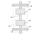
図1に、本実施の形態のスタンダードセルの模式図を示す。図1のスタンダードセル108は、VDD用電源ライン101、GND用電源ライン102、テストパッド103〜104、及び配線105〜107を有している。なお、VDD用電源ライン101、GND用電源ライン102、テストパッド103〜104、及び配線105〜107は導電性の材料で形成されている。また、テストパッド103とテストパッド104とは配線105によって電気的に接続されている。また、配線106はテストパッド103と接続し、配線107はテストパッド104と接続する。ここで、配線106は入力用ポートとして機能し、配線107は出力用ポートとして機能する。入力用ポートおよび出力用ポートを介して他のスタンダードセルや回路ブロックとの信号のやり取りを行うことができる。本実施の形態では、配線105〜107、テストパッド103、104を同一直線上に設けているため、テストパッド用のスタンダードセルの幅を小さくすることができる。スタンダードセルの幅を小さくすることで、回路面積の縮小ができ、消費電力の削減を行うことができる。
FIG. 1 shows a schematic diagram of a standard cell of the present embodiment. The
そして、スタンダードセル108を回路の構成単位として、他のスタンダードセル(例えば、インバータ回路、NAND回路、NOR回路、フリップフロップ回路等)とともに自動レイアウトにて配置することで所望の機能を有する半導体集積回路を得ることができる。つまり、図1の配線106、107は他のスタンダードセルとそれぞれ接続されており、テストパッド103、104それぞれは配線106、107を介して他のスタンダードセルと電気的に接続されている。
A semiconductor integrated circuit having a desired function by being arranged in an automatic layout together with other standard cells (for example, an inverter circuit, a NAND circuit, a NOR circuit, a flip-flop circuit, etc.) with the
次に、自動レイアウトで所望の回路を構成した後、テストパッド103、104を用いて特定の端子の電流を測定する方法について説明する。なお、スタンダードセルは、テストパッド103、104が配線105で接続されている状態では、入力用ポート106から流れこんだ電流は、テストパッド103、配線105、テストパッド104を通して出力用ポート107に流れる。ここで、テストパッド103又はテストパッド104を電圧測定用のテストパッドとして用いて任意の端子の電圧を測定して、電流を測定したい端子の特定を行ってもよい。
Next, a method of measuring a current at a specific terminal using the
そして、電流を測定したい端子に対応するテストパッド(ここでは、テストパッド103、104とする(図1))を選択し、2つのテストパッドを接続する配線(ここでは、配線105に相当する(図1))を、レーザー等を用いて切断する。これにより、2つのテストパッド103、104の間は絶縁化される。そして、絶縁された2つのテストパッド103、104それぞれに電流測定器の針を当てて電流を測定して不良箇所を特定する。
Then, a test pad corresponding to a terminal whose current is to be measured (here, referred to as
また、本実施の形態において、スタンダードセルの配置領域外である配線領域などの狭く、配線の密に並んだ領域にテストパッドを設ける必要がないため、テストパッドを設けるためのレイアウト修正を大規模に行う必要がなく、レイアウト修正時のレイアウトミスを防ぐことができる。さらに、レイアウト修正のために費やす時間も少なくできる。さらに、テストパッドを含むスタンダードセルを他のスタンダードセルと同じ領域内に配置することができるため、テストパッドの配置面積を大きくとることが可能となる。よって電流測定器の針を当てる作業がより簡単なものになる。また測定する信号線以外の配線がテストパッドよりも遠い場所にあるため、電流測定器の針をあてる作業が失敗したときなどに、他の配線にダメージを与える可能性を低くすることができる。 Further, in this embodiment, since it is not necessary to provide test pads in a narrow and densely lined area such as a wiring area outside the standard cell arrangement area, layout correction for providing the test pad is performed on a large scale. Therefore, it is possible to prevent layout mistakes during layout correction. Furthermore, the time spent for layout correction can be reduced. Furthermore, since the standard cell including the test pad can be arranged in the same region as other standard cells, it is possible to increase the arrangement area of the test pad. Therefore, the operation of applying the current measuring instrument needle becomes easier. Further, since the wiring other than the signal line to be measured is located far from the test pad, the possibility of damaging the other wiring when the operation of applying the needle of the current measuring device fails can be reduced.
また、本実施の形態において、2つのテストパッドを有するスタンダードセルを自動レイアウトで配置した後、2つのテストパッド間を接続する配線を切断することでテストパッド間を絶縁状態としている。従って、チップ毎にそれぞれ電流測定端子を容易に変えることができる。本実施の形態のスタンダードセルを用いることで、チップ毎に電流測定を行う端子が変化した場合でもマスク変更を行う必要がないため、低コストな半導体装置を作製することが可能である。また、2つのテストパッド間の配線を切断する前の状態では、電圧測定を行うことが可能であり、テストパッドを2つ有することで一方のテストパッドが測定不能になった場合には他方のテストパッドで測定可能であり、繰り返し試験への耐性を向上させることが可能である。 Further, in the present embodiment, after standard cells having two test pads are arranged in an automatic layout, the wiring connecting the two test pads is cut to isolate the test pads. Therefore, the current measurement terminals can be easily changed for each chip. By using the standard cell of this embodiment mode, it is not necessary to change the mask even when the terminal for current measurement is changed for each chip, so that a low-cost semiconductor device can be manufactured. In addition, voltage measurement can be performed in a state before the wiring between the two test pads is cut. When one test pad becomes impossible to measure by having two test pads, the other It can be measured with a test pad and can improve resistance to repeated tests.
また、本実施の形態において、他の回路ブロックや、スタンダードセルの近くに電流測定用のテストパッドを設けることができるため、信号が生成された直後の場所で電流測定が行うことができる。また、引き回し配線が短くなるため、長い引き回しが原因の信号の減衰などの影響を少なくできる。さらに、ノイズが乗る可能性を低く抑えることができるため、回路の動作をより安定したものにできる。長い引き回し配線が原因として起きる寄生容量の増加や、消費電流の増加を抑えることができる。 In the present embodiment, since a test pad for current measurement can be provided near another circuit block or standard cell, current measurement can be performed immediately after the signal is generated. In addition, since the routing wiring is shortened, the influence of signal attenuation caused by the long routing can be reduced. Further, since the possibility of noise is reduced, the circuit operation can be made more stable. It is possible to suppress an increase in parasitic capacitance and an increase in current consumption caused by a long lead wiring.
また、電流測定の必要がなくなり、テストパッドを削除する際の作業も容易である。具体的には、スタンダードセル内にある2つのテストパッドを削除することで、本発明のスタンダードセルは信号を伝送する機能を有するフィードセルになる。テストパッドの削除は、マスク1枚の変更のみで対応できるため、削除する際のコストを低減することができる。 Also, there is no need for current measurement, and the work for deleting the test pad is easy. Specifically, by deleting two test pads in the standard cell, the standard cell of the present invention becomes a feed cell having a function of transmitting a signal. Since the test pad can be deleted only by changing one mask, the cost for deleting the test pad can be reduced.
(実施の形態2)
本実施の形態では、実施の形態1とは異なる構成のスタンダードセルについて説明する。本実施の形態で示すスタンダードセルは、過電流が流れた際に、2つのテストパッド間が絶縁化される構成を有する。
(Embodiment 2)
In the present embodiment, a standard cell having a configuration different from that of the first embodiment will be described. The standard cell shown in this embodiment has a configuration in which two test pads are insulated when an overcurrent flows.
図2に、本実施の形態のスタンダードセルの模式図を示す。図2のスタンダードセル208は、VDD用電源ライン201、GND用電源ライン202、テストパッド203〜204、及び配線205〜207を有している。なお、VDD用電源ライン201、GND用電源ライン202、テストパッド203〜204、及び配線205〜207は導電性の材料で形成されている。また、テストパッド203とテストパッド204とは配線205によって電気的に接続されている。また、配線206はテストパッド203と接続し、配線207はテストパッド204と接続する。ここで、配線206は入力用ポートとして機能し、配線207は出力用ポートとして機能する。入力用ポートおよび出力用ポートを介して他のスタンダードセルや回路ブロックとの信号のやり取りを行うことができる。本実施の形態では、配線205〜207、テストパッド203、204を同一直線上に設けているため、テストパッド用のスタンダードセルの幅を小さくすることができる。スタンダードセルの幅を小さくすることで、回路面積の縮小ができ、消費電力の削減を行うことができる。
FIG. 2 shows a schematic diagram of the standard cell of the present embodiment. The
本実施の形態では、配線205に基準よりも大きい電流(過電流)が流れた際に、テストパッド203とテストパッド204とが絶縁化される構成とする。そこで、本実施の形態のテストパッドは、2つのテストパッド間を結ぶ配線205の幅が均一ではなく、部分的に抵抗が異なる構成とする。
In this embodiment mode, the
そして、スタンダードセル208を回路の構成単位として、他のスタンダードセル(例えば、インバータ回路、NAND回路、NOR回路、フリップフロップ回路等)とともに自動レイアウトにて配置することで所望の機能を有する半導体集積回路を得ることができる。
A semiconductor integrated circuit having a desired function by being arranged in an automatic layout together with other standard cells (for example, an inverter circuit, a NAND circuit, a NOR circuit, a flip-flop circuit, etc.) using the
次に、自動レイアウトで所望の回路を構成した後、テストパッド203、204を用いて特定の端子の電流を測定する方法について説明する。なお、スタンダードセルは、テストパッド203、204が配線205で接続されている状態では、入力用ポート206から流れこんだ電流は、テストパッド203、配線205、テストパッド204を通して出力用ポート207に流れ、出力ポートから他のスタンダードセルに供給される。ここで、テストパッド203又はテストパッド204を電圧測定用のテストパッドとして用いて任意の端子の電圧を測定して、電流を測定したい端子の特定を行ってもよい。
Next, a method of measuring a current at a specific terminal using the
ここで説明を簡単にするために、配線205を配線領域209、210、211とに分けて説明する。ここで、配線領域211は、横幅と長さを配線領域209、210に比べて幅と長さを小さく形成する。つまり、配線領域209、210は、211に比べて幅を広く形成しておく。これにより、配線領域209、210の部分の配線抵抗を配線領域211の配線抵抗に比べて小さくすることができる。配線領域211部分が他の領域に比べて抵抗が高くなるため、そして、この配線部211に大きな電流が流れると、211が絶縁化される。
Here, in order to simplify the description, the
なお、本実施の形態において配線211の材料及び大きさによって、配線211を切断するために必要な電流値は変化する。配線を溶かすために必要な熱量は、配線の質量に比例するため、配線部211の領域の質量が大きければ、配線211を溶かすために必要な熱量も増えるためである。つまり、配線211の質量が増加するほどより大きな電流を流さないと配線211は溶けず、2つのテストパッド203、204間は絶縁化されない。本実施の形態では、この性質を利用することにより、配線211の大きさ、配線211に流れる電流の最大値、該電流が流れる時間等を任意に設定することができる。
Note that in this embodiment mode, a current value required for cutting the
ここで、図2(B)を用いて、図2(A)で示したスタンダードセルのテストパッド203とテストパッド204間の絶縁化の方法について具体的な例を挙げて説明する。図2(B)は、図2(A)の配線205部分の傾斜図である。ここで、配線205としてアルミニウムを用いた場合について説明する。アルミニウムは、融点約600℃、密度2.9g/cm3、比熱0.88J/g・Kである。本実施例では、配線領域211において、厚さdが700nm、長さlが2μm、幅vが2μmのアルミニウムを用いた場合に、配線211が断線されるまでの工程を説明する。ここで、配線211に電流100μA、電圧5Vが供給される場合を考える。なお、この値は、シュミレーション等を用いて、回路に必要な電流値から適宜選択されるものである。
Here, with reference to FIG. 2B, a method of insulating between the
配線部211に流れる電流で発生するジュール熱は、500×10―6×t(J)と表される。ここで、tは電流を流す時間(単位は秒)である。一方、図2の領域のアルミニウムを溶かすためには、アルミニウムの温度をアルミニウムの融点である600度付近まで上げるためのジュール熱が必要となるが、そのジュール熱は4.287×10―9(J)である。以上のことから、100μAの電流を10μs流すことで配線211の温度は600度以上になる。従って、100μAの電流を10μs以上流すことで配線領域211のアルミニウムが溶け出し、配線領域211の配線が切れ、配線領域209と配線領域210の間は絶縁状態になる。
Joule heat generated by the current flowing through the
なお、ここでは、あらかじめ配線211の大きさ及び配線211に供給される電流、電圧の最大値を設定し、配線211が切断されるまでに必要な時間を求めたが、この方法に限定されるものではない。例えば、配線211に供給される電流、電圧の最大値及び切断されるまでに必要な時間を設定し、それに基づいて配線211の大きさ(質量、厚さ、幅、長さ等)を設定する方法としてもよい。
Note that here, the size of the
本実施の形態において、回路を動作させただけで過電流の流れる配線を切断できるため、回路内の不良箇所を容易に検出することが可能である。測定時に、テストパッド毎に測定して不良箇所を特定する作業が必要ないため、回路を検査に必要な時間が大幅に短縮できる。また、マスク変更や特別な手段を用いて2つのテストパッド間を接続する配線を切断する作業が必要ないため、回路内の不良箇所の検出を容易に行うことができる。 In this embodiment mode, the wiring through which the overcurrent flows can be cut only by operating the circuit, so that a defective portion in the circuit can be easily detected. At the time of measurement, it is not necessary to perform measurement for each test pad to identify a defective portion, so that the time required for inspecting the circuit can be greatly shortened. Further, since it is not necessary to cut the wiring connecting the two test pads using a mask change or special means, it is possible to easily detect a defective portion in the circuit.
また、本実施の形態において、スタンダードセルの配置領域外である配線領域などの狭く、配線の密に並んだ領域にテストパッドを設ける必要がないため、テストパッドを設けるためのレイアウト修正を大規模に行う必要がなく、レイアウト修正時のレイアウトミスを防ぐことができる。さらに、レイアウト修正のために費やす時間も少なくできる。さらに、テストパッドを含むスタンダードセルを他のスタンダードセルと同じ領域内に配置することができるため、テストパッドの配置面積を大きくとることが可能となる。よって電流測定器の針を当てる作業がより簡単なものになる。また測定する信号線以外の配線がテストパッドよりも遠い場所にあるため、電流測定器の針をあてる作業が失敗したときなどに、他の配線にダメージを与える可能性を低くすることができる。 Further, in this embodiment, since it is not necessary to provide test pads in a narrow and densely lined area such as a wiring area outside the standard cell arrangement area, layout correction for providing the test pad is performed on a large scale. Therefore, it is possible to prevent layout mistakes during layout correction. Furthermore, the time spent for layout correction can be reduced. Furthermore, since the standard cell including the test pad can be arranged in the same region as other standard cells, it is possible to increase the arrangement area of the test pad. Therefore, the operation of applying the current measuring instrument needle becomes easier. Further, since the wiring other than the signal line to be measured is located far from the test pad, the possibility of damaging the other wiring when the operation of applying the needle of the current measuring device fails can be reduced.
また、本実施の形態において、2つのテストパッドを有するスタンダードセルを自動レイアウトで配置した後、2つのテストパッド間を接続する配線を切断することでテストパッド間を絶縁状態としている。従って、チップ毎にそれぞれ電流測定端子を容易に変えることができる。本実施の形態のスタンダードセルを用いることで、チップ毎に電流測定を行う端子が変化した場合でもマスク変更を行う必要がないため、低コストな半導体装置を作製することが可能である。また、2つのテストパッド間の配線を切断する前の状態では、電圧測定を行うことが可能であり、テストパッドを2つ有することで一方のテストパッドが測定不能になった場合には他方のテストパッドで測定可能であり、繰り返し試験への耐性を向上させることが可能である。 Further, in the present embodiment, after standard cells having two test pads are arranged in an automatic layout, the wiring connecting the two test pads is cut to isolate the test pads. Therefore, the current measurement terminals can be easily changed for each chip. By using the standard cell of this embodiment mode, it is not necessary to change the mask even when the terminal for current measurement is changed for each chip, so that a low-cost semiconductor device can be manufactured. In addition, voltage measurement can be performed in a state before the wiring between the two test pads is cut. When one test pad becomes impossible to measure by having two test pads, the other It can be measured with a test pad and can improve resistance to repeated tests.
また、本実施の形態において、他の回路ブロックや、スタンダードセルの近くに電流測定用のテストパッドを設けることができるため、信号が生成された直後の場所で電流測定が行うことができる。また、引き回し配線が短くなるため、長い引き回しが原因の信号の減衰などの影響を少なくできる。さらに、ノイズが乗る可能性を低く抑えることができるため、回路の動作をより安定したものにできる。長い引き回し配線が原因として起きる寄生容量の増加や、消費電流の増加を抑えることができる。 In the present embodiment, since a test pad for current measurement can be provided near another circuit block or standard cell, current measurement can be performed immediately after the signal is generated. In addition, since the routing wiring is shortened, the influence of signal attenuation caused by the long routing can be reduced. Further, since the possibility of noise is reduced, the circuit operation can be made more stable. It is possible to suppress an increase in parasitic capacitance and an increase in current consumption caused by a long lead wiring.
また、電流測定の必要がなくなり、テストパッドを削除する際の作業も容易である。具体的には、スタンダードセル内にある2つのテストパッドを削除することで、本発明のスタンダードセルは信号を伝送する機能を有するフィードセルになる。テストパッドの削除は、マスク1枚の変更のみで対応できるため、削除する際のコストを低減することができる。 Also, there is no need for current measurement, and the work for deleting the test pad is easy. Specifically, by deleting two test pads in the standard cell, the standard cell of the present invention becomes a feed cell having a function of transmitting a signal. Since the test pad can be deleted only by changing one mask, the cost for deleting the test pad can be reduced.
(実施の形態3)
本実施の形態において、2つのテストパッドを接続する配線としてメモリ素子を用いる場合について説明する。
(Embodiment 3)
In this embodiment mode, a case where a memory element is used as a wiring connecting two test pads will be described.
図3にメモリ素子を含むスタンダードセルの回路図を示す。図3に示すスタンダードセル308は、VDD用電源ライン301、GND用電源ライン302、テストパッド303、304、メモリ素子305、電流入力用ポート306および電流出力用ポート307を有する。
FIG. 3 shows a circuit diagram of a standard cell including a memory element. A
そして、スタンダードセル308を回路の構成単位として、他のスタンダードセル(例えば、インバータ回路、NAND回路、NOR回路、フリップフロップ回路等)とともに自動レイアウトにて配置することで所望の機能を有する半導体集積回路を得ることができる。
A semiconductor integrated circuit having a desired function by being arranged in an automatic layout together with other standard cells (for example, an inverter circuit, a NAND circuit, a NOR circuit, a flip-flop circuit, etc.) using the
本実施の形態において、メモリ素子305として、電流による発熱で状態が変化し、抵抗が変化するメモリを用いる。そのようなメモリとして、例えば相変化メモリが挙げられる。相変化メモリは、回路に電流が多く流れた場合、メモリ素子にふくまれるヒーターが熱を発生し、電流量が多い場合には発熱量が多くなり、相変化をする物質(Ge2Sb2Te5など)がアモルファス状態になり、電気抵抗が高くなり絶縁化される。本実施の形態において、この変化を利用することで、2つのテストパッド303、304間を絶縁化して電流測定を行うことができる。なお、もちろんメモリ305は相変化メモリに限られるものではない。電流が多く流れたところの素子のみ絶縁化を行い、2つのテストパッド303、304の間を絶縁状態にすることができればどのようなものでもよい。例えば、メモリとして、流れる電流量により抵抗が変化するRRAMを用いることもできる。
In this embodiment, as the
図3の回路動作について説明を行う。メモリ素子305は初期状態では導通している。そのため、通常の回路として使用できる。この回路に大きな電流が流れた場合、メモリ素子305が非導通になる。その際にスタンダードセル内に含まれる2つのテストパッド303、304に電流測定器の針を当て、電流測定を行うことができる。
The circuit operation of FIG. 3 will be described. The
本実施の形態において、回路を動作させただけで過電流の流れる配線を切断できるため、回路内の不良箇所を容易に検出することが可能である。測定時に、テストパッド毎に測定して不良箇所を特定する作業が必要ないため、回路を検査に必要な時間が大幅に短縮できる。さらに、マスク変更や特別な手段を用いて2つのテストパッド間を接続する配線を切断する作業が必要ないため、回路内の不良箇所の検出を容易に行うことができる。また、可逆反応を用いたメモリを利用するため、一度絶縁状態になった配線を元の状態に戻すことも可能である。 In this embodiment mode, the wiring through which the overcurrent flows can be cut only by operating the circuit, so that a defective portion in the circuit can be easily detected. At the time of measurement, it is not necessary to perform measurement for each test pad to identify a defective portion, so that the time required for inspecting the circuit can be greatly shortened. Furthermore, since it is not necessary to cut the wiring connecting the two test pads using a mask change or special means, it is possible to easily detect a defective portion in the circuit. In addition, since a memory using a reversible reaction is used, it is possible to return a wiring that has been once insulated to its original state.
また、本実施の形態において、スタンダードセルの配置領域外である配線領域などの狭く、配線の密に並んだ領域にテストパッドを設ける必要がないため、テストパッドを設けるためのレイアウト修正を大規模に行う必要がなく、レイアウト修正時のレイアウトミスを防ぐことができる。さらに、レイアウト修正のために費やす時間も少なくできる。さらに、テストパッドを含むスタンダードセルを他のスタンダードセルと同じ領域内に配置することができるため、テストパッドの配置面積を大きくとることが可能となる。よって電流測定器の針を当てる作業がより簡単なものになる。また測定する信号線以外の配線がテストパッドよりも遠い場所にあるため、電流測定器の針をあてる作業が失敗したときなどに、他の配線にダメージを与える可能性を低くすることができる。 Further, in this embodiment, since it is not necessary to provide test pads in a narrow and densely lined area such as a wiring area outside the standard cell arrangement area, layout correction for providing the test pad is performed on a large scale. Therefore, it is possible to prevent layout mistakes during layout correction. Furthermore, the time spent for layout correction can be reduced. Furthermore, since the standard cell including the test pad can be arranged in the same region as other standard cells, it is possible to increase the arrangement area of the test pad. Therefore, the operation of applying the current measuring instrument needle becomes easier. Further, since the wiring other than the signal line to be measured is located far from the test pad, the possibility of damaging the other wiring when the operation of applying the needle of the current measuring device fails can be reduced.
また、本実施の形態において、2つのテストパッドを有するスタンダードセルを自動レイアウトで配置した後、2つのテストパッド間を接続する配線を切断することでテストパッド間を絶縁状態としている。従って、チップ毎にそれぞれ電流測定端子を容易に変えることができる。本実施の形態のスタンダードセルを用いることで、チップ毎に電流測定を行う端子が変化した場合でもマスク変更を行う必要がないため、低コストな半導体装置を作製することが可能である。また、2つのテストパッド間の配線を切断する前の状態では、電圧測定を行うことが可能であり、テストパッドを2つ有することで一方のテストパッドが測定不能になった場合には他方のテストパッドで測定可能であり、繰り返し試験への耐性を向上させることが可能である。 Further, in the present embodiment, after standard cells having two test pads are arranged in an automatic layout, the wiring connecting the two test pads is cut to isolate the test pads. Therefore, the current measurement terminals can be easily changed for each chip. By using the standard cell of this embodiment mode, it is not necessary to change the mask even when the terminal for current measurement is changed for each chip, so that a low-cost semiconductor device can be manufactured. In addition, voltage measurement can be performed in a state before the wiring between the two test pads is cut. When one test pad becomes impossible to measure by having two test pads, the other It can be measured with a test pad and can improve resistance to repeated tests.
また、本実施の形態において、他の回路ブロックや、スタンダードセルの近くに電流測定用のテストパッドを設けることができるため、信号が生成された直後の場所で電流測定が行うことができる。また、引き回し配線が短くなるため、長い引き回しが原因の信号の減衰などの影響を少なくできる。さらに、ノイズが乗る可能性を低く抑えることができるため、回路の動作をより安定したものにできる。長い引き回し配線が原因として起きる寄生容量の増加や、消費電流の増加を抑えることができる。 In the present embodiment, since a test pad for current measurement can be provided near another circuit block or standard cell, current measurement can be performed immediately after the signal is generated. In addition, since the routing wiring is shortened, the influence of signal attenuation caused by the long routing can be reduced. Further, since the possibility of noise is reduced, the circuit operation can be made more stable. It is possible to suppress an increase in parasitic capacitance and an increase in current consumption caused by a long lead wiring.
また、電流測定の必要がなくなり、テストパッドを削除する際の作業も容易である。具体的には、スタンダードセル内にある2つのテストパッドを削除することで、本発明のスタンダードセルは信号を伝送する機能を有するフィードセルになる。テストパッドの削除は、マスク1枚の変更のみで対応できるため、削除する際のコストを低減することができる。 Also, there is no need for current measurement, and the work for deleting the test pad is easy. Specifically, by deleting two test pads in the standard cell, the standard cell of the present invention becomes a feed cell having a function of transmitting a signal. Since the test pad can be deleted only by changing one mask, the cost for deleting the test pad can be reduced.
(実施の形態4)
本実施の形態において、2つのテストパッド間がアナログスイッチを介して接続されている構成について説明する。
(Embodiment 4)
In the present embodiment, a configuration in which two test pads are connected via an analog switch will be described.
図4にアナログスイッチを含むスタンダードセルの回路図を示す。スタンダードセル408は、VDD用電源ライン401、GND用電源ライン402、テストパッド403、テストパッド404、アナログスイッチ409、インバータ410、電流制御信号入力ポート405、電流入力用ポート406および電流出力用ポート407を有する。
FIG. 4 shows a circuit diagram of a standard cell including an analog switch. The
そして、スタンダードセル408を回路の構成単位として、他のスタンダードセル(例えば、インバータ回路、NAND回路、NOR回路、フリップフロップ回路等)とともに自動レイアウトにて配置することで所望の機能を有する半導体集積回路を得ることができる。
A semiconductor integrated circuit having a desired function by being arranged in an automatic layout together with other standard cells (for example, an inverter circuit, a NAND circuit, a NOR circuit, a flip-flop circuit, etc.) using the
図4に示す回路はアナログスイッチ409によってのテストパッド403およびテストパッド404間の接続状態、つまり導通状態と非道通状態を変化させることができる。例えば、電流制御信号入力ポート405にLowの信号が入力された場合、アナログスイッチ409は導通状態となり、通常の回路として用いることができる。ここで、電流制御信号入力ポート405にHiの信号を入力した場合、アナログスイッチ409は非導通状態となり電流を測定することが可能となる。
The circuit shown in FIG. 4 can change the connection state between the
そして、スタンダードセル408を回路の構成単位として、他のスタンダードセル(例えば、インバータ回路、NAND回路、NOR回路、フリップフロップ回路等)とともに自動レイアウトにて配置することで所望の機能を有する回路を得ることができる。
A circuit having a desired function is obtained by arranging the
本実施の形態において、2つのテストパッド間の導通又は非導通を電圧信号の変化という簡単な方法で切り替えることができる。本実施の形態では、スイッチを用いてテストパッド間の導通又は非導通を切り換えているため、導通又は非導通を繰り返すことが可能である。テスト用のサンプルが少ない場合などに、サンプルを繰り返し利用できる。 In the present embodiment, conduction or non-conduction between two test pads can be switched by a simple method of changing a voltage signal. In this embodiment, since conduction or non-conduction between test pads is switched using a switch, conduction or non-conduction can be repeated. Samples can be used repeatedly when there are few samples for testing.
また、本実施の形態において、スタンダードセルの配置領域外である配線領域などの狭く、配線の密に並んだ領域にテストパッドを設ける必要がないため、テストパッドを設けるためのレイアウト修正を大規模に行う必要がなく、レイアウト修正時のレイアウトミスを防ぐことができる。さらに、レイアウト修正のために費やす時間も少なくできる。さらに、テストパッドを含むスタンダードセルを他のスタンダードセルと同じ領域内に配置することができるため、テストパッドの配置面積を大きくとることが可能となる。よって電流測定器の針を当てる作業がより簡単なものになる。また測定する信号線以外の配線がテストパッドよりも遠い場所にあるため、電流測定器の針をあてる作業が失敗したときなどに、他の配線にダメージを与える可能性を低くすることができる。 Further, in this embodiment, since it is not necessary to provide test pads in a narrow and densely lined area such as a wiring area outside the standard cell arrangement area, layout correction for providing the test pad is performed on a large scale. Therefore, it is possible to prevent layout mistakes during layout correction. Furthermore, the time spent for layout correction can be reduced. Furthermore, since the standard cell including the test pad can be arranged in the same region as other standard cells, it is possible to increase the arrangement area of the test pad. Therefore, the operation of applying the current measuring instrument needle becomes easier. Further, since the wiring other than the signal line to be measured is located far from the test pad, the possibility of damaging the other wiring when the operation of applying the needle of the current measuring device fails can be reduced.
また、本実施の形態において、2つのテストパッドを有するスタンダードセルを自動レイアウトで配置した後、2つのテストパッド間を接続する配線を切断することでテストパッド間を絶縁状態としている。従って、チップ毎にそれぞれ電流測定端子を容易に変えることができる。本実施の形態のスタンダードセルを用いることで、チップ毎に電流測定を行う端子が変化した場合でもマスク変更を行う必要がないため、低コストな半導体装置を作製することが可能である。また、2つのテストパッド間の配線を切断する前の状態では、電圧測定を行うことが可能であり、テストパッドを2つ有することで一方のテストパッドが測定不能になった場合には他方のテストパッドで測定可能であり、繰り返し試験への耐性を向上させることが可能である。 Further, in the present embodiment, after standard cells having two test pads are arranged in an automatic layout, the wiring connecting the two test pads is cut to isolate the test pads. Therefore, the current measurement terminals can be easily changed for each chip. By using the standard cell of this embodiment mode, it is not necessary to change the mask even when the terminal for current measurement is changed for each chip, so that a low-cost semiconductor device can be manufactured. In addition, voltage measurement can be performed in a state before the wiring between the two test pads is cut. When one test pad becomes impossible to measure by having two test pads, the other It can be measured with a test pad and can improve resistance to repeated tests.
また、本実施の形態において、他の回路ブロックや、スタンダードセルの近くに電流測定用のテストパッドを設けることができるため、信号が生成された直後の場所で電流測定が行うことができる。また、引き回し配線が短くなるため、長い引き回しが原因の信号の減衰などの影響を少なくできる。さらに、ノイズが乗る可能性を低く抑えることができるため、回路の動作をより安定したものにできる。長い引き回し配線が原因として起きる寄生容量の増加や、消費電流の増加を抑えることができる。 In the present embodiment, since a test pad for current measurement can be provided near another circuit block or standard cell, current measurement can be performed immediately after the signal is generated. In addition, since the routing wiring is shortened, the influence of signal attenuation caused by the long routing can be reduced. Further, since the possibility of noise is reduced, the circuit operation can be made more stable. It is possible to suppress an increase in parasitic capacitance and an increase in current consumption caused by a long lead wiring.
また、電流測定の必要がなくなり、テストパッドを削除する際の作業も容易である。具体的には、スタンダードセル内にある2つのテストパッドを削除することで、本発明のスタンダードセルは信号を伝送する機能を有するフィードセルになる。テストパッドの削除は、マスク1枚の変更のみで対応できるため、削除する際のコストを低減することができる。 Also, there is no need for current measurement, and the work for deleting the test pad is easy. Specifically, by deleting two test pads in the standard cell, the standard cell of the present invention becomes a feed cell having a function of transmitting a signal. Since the test pad can be deleted only by changing one mask, the cost for deleting the test pad can be reduced.
(実施の形態5)
本実施の形態において、上記実施の形態とは異なるテストパッド及び配線の配置方法について説明する。図5に本実施の形態のスタンダードセルの構成を示す。
(Embodiment 5)
In this embodiment mode, a method for arranging test pads and wirings different from the above embodiment mode will be described. FIG. 5 shows the configuration of the standard cell of this embodiment.
図5のスタンダードセル508は、VDD用電源ライン501、GND用電源ライン502、テストパッド503、テストパッド504、及び配線505〜507を有している。本実施の形態では、配線506、507とVDD用電源ライン501、GND用電源ライン502とは平行に配置され、配線505とVDD用電源ライン501、GND用電源ライン502とは垂直に配置される。なお、VDD用電源ライン501、GND用電源ライン502、テストパッド503〜504、及び配線505〜507は導電性の材料で形成されている。また、テストパッド503とテストパッド504とは配線505によって電気的に接続されている。また、配線506はテストパッド503と接続し、配線507はテストパッド504と接続する。ここで、配線506は入力用ポートとして機能し、配線507は出力用ポートとして機能する。入力用ポートおよび出力用ポートを介して他のスタンダードセルや回路ブロックとの信号のやり取りを行うことができる。
A
そして、スタンダードセル508を回路の構成単位として、他のスタンダードセル(例えば、インバータ回路、NAND回路、NOR回路、フリップフロップ回路等)とともに自動レイアウトにて配置することで所望の機能を有する半導体集積回路を得ることができる。
A semiconductor integrated circuit having a desired function by being arranged in an automatic layout together with other standard cells (for example, an inverter circuit, a NAND circuit, a NOR circuit, a flip-flop circuit, etc.) using the
本実施の形態では、配線506、507とVDD用電源ライン501、GND用電源ライン502とは平行に配置しているため、入力用の信号と出力用の信号が同じ方向から出入りする場合に引き回しに必要な配線をより短くすることができる。例えば、回路の外周領域にテストパッドを有するスタンダードセルを配置する場合、引き回し配線をより短くすることが可能である。
In this embodiment mode, the
また、必ずしも配線506、507とVDD用電源ライン501、GND用電源ライン502とが平行に配置されていなくてもよく、配線が密になっている箇所にテストパッドを有するスタンダードセルを配置する場合は、配線が密である領域を避けてそれぞれの信号線が接続されるような配置にすればよい。例えば、図6に示す配置をとることができる。
In addition, the
図6に示すスタンダードセル608は、VDD用電源ライン601と、GND用電源ライン602、テストパッド603、テストパッド604、及び配線605〜607を有している。本実施の形態では、配線606、607とVDD用電源ライン601、GND用電源ライン602とは垂直に配置され、配線605とVDD用電源ライン601、GND用電源ライン602とは平行に配置される。また、配線606とVDD電源ライン601とが交叉し、配線607とGND電源ライン602とが交叉している。なお、VDD用電源ライン601、GND用電源ライン602、テストパッド603〜604、及び配線605〜607は導電性の材料で形成されている。また、テストパッド603とテストパッド604とは配線605によって電気的に接続されている。また、配線606はテストパッド603と接続し、配線607はテストパッド604と接続する。ここで、配線606は入力用ポートとして機能し、配線607は出力用ポートとして機能する。入力用ポートおよび出力用ポートを介して他のスタンダードセルや回路ブロックとの信号のやり取りを行うことができる。
A
そして、スタンダードセル608を回路の構成単位として、他のスタンダードセル(例えば、インバータ回路、NAND回路、NOR回路、フリップフロップ回路等)とともに自動レイアウトにて配置することで所望の機能を有する半導体集積回路を得ることができる。
A semiconductor integrated circuit having a desired function by being arranged in an automatic layout together with other standard cells (for example, an inverter circuit, a NAND circuit, a NOR circuit, a flip-flop circuit, etc.) using the
図6に示すスタンダードセルにおいて、配線606とVDD電源ライン601とが交叉し、配線607とGND電源ライン602とが交叉するように配置されているため、テストパッド603をGND電源ライン602方向に大きくでき、テストパッド604をVDD電源ライン603方向に大きくできる。これにより、測定時のパッド探しの作業および針あての作業をより容易に行うことができる。さらに、図6に示すスタンダードセルでは、テストパッド603、604は、VDD電源ライン601及びGND電源ライン602と平行に配置されているため、VDD電源ライン601およびGND電源ライン602から離れた位置にテストパッド603、604を配置することができる。そのため、電流を測定する際に、スタンダードセル608に含まれるVDD電源ライン601又はGND電源ライン602に供給される電圧、電流による影響を受けにくく、より正確に電流値を測定できる。
In the standard cell shown in FIG. 6, since the
なお、入力用ポート606と出力用ポート607の位置は図6に示したものに限られず、テストパッドを含むスタンダードセルの配置によって、それぞれの配線が最も適切に行われるように配置されていればよい。
Note that the positions of the
(実施の形態6)
本実施の形態において、上記実施の形態とは異なるテストパッド及び配線の配置方法について説明する。図7に本実施の形態のスタンダードセルの構成を示す。
(Embodiment 6)
In this embodiment mode, a method for arranging test pads and wirings different from the above embodiment mode will be described. FIG. 7 shows the configuration of the standard cell of this embodiment.
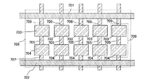
図7に示すスタンダードセル708は、VDD用電源ライン701と、GND用電源ライン702、複数のテストパッド703、704、複数の配線705〜707を有している。図7において、1つのテストパッド703と1つのテストパッド704とは1本の配線705によって電気的に接続されている。また、1本の配線706は1つのテストパッド703と接続し、1本の配線707は1つのテストパッド704と接続している。該配線705で接続された該テストパッド703、704とで一組の電流測定TEG709が構成されている。ここで、配線706は入力用ポートとして機能し、配線707は出力用ポートとして機能する。入力用ポートおよび出力用ポートを介して他のスタンダードセルや回路ブロックとの信号のやり取りを行うことができる。なお、本実施の形態において、配線705〜707は同一直線上に配置されているがこの構成に限定されない。また、VDD用電源ライン701、GND用電源ライン702、テストパッド703〜704、及び配線705〜707は導電性の材料で形成されている。
A
そして、スタンダードセル708を回路の構成単位として、他のスタンダードセル(例えば、インバータ回路、NAND回路、NOR回路、フリップフロップ回路等)とともに自動レイアウトにて配置することで所望の機能を有する半導体集積回路を得ることができる。
A semiconductor integrated circuit having a desired function by being arranged in an automatic layout together with other standard cells (for example, an inverter circuit, a NAND circuit, a NOR circuit, a flip-flop circuit, etc.) using the
図7に示すスタンダードセルでは、種々の信号線をひとつのスタンダードセルにまとめることができるため、レイアウト時の信号線の管理が容易になる。また、電流測定時にパッドを探す手間が省ける。さらに、異なる信号間のテストパッドの距離が大きく離れていないため、電流測定器の針の移動も容易となる。また、テストパッド間の大きさを調整することで、複数の電流を一括して測定することもでき、回路検証をより効率的に進めることが可能となる。 In the standard cell shown in FIG. 7, since various signal lines can be combined into one standard cell, management of the signal lines at the time of layout becomes easy. Moreover, the trouble of searching for a pad during current measurement can be saved. Furthermore, since the distance of the test pad between different signals is not greatly separated, the movement of the stylus of the ampere meter is facilitated. In addition, by adjusting the size between the test pads, it is possible to measure a plurality of currents in a lump, and circuit verification can be promoted more efficiently.
他の構成として図8に示す構成としてもよい。図8のスタンダードセル808は、VDD用電源ライン801と、GND用電源ライン802、複数のテストパッド803、804、複数の配線805〜807を有している。図8において、1つのテストパッド803と1つのテストパッド804とは1本の配線805によって電気的に接続されている。また、1本の配線806は1つのテストパッド803と接続し、1本の配線807は1つのテストパッド804と接続している。該配線805で接続された該テストパッド803、804とで一組の電流測定TEG809が構成されている。ここで、配線806は入力用ポートとして機能し、配線807は出力用ポートとして機能する。入力用ポートおよび出力用ポートを介して他のスタンダードセルや回路ブロックとの信号のやり取りを行うことができる。なお、本実施の形態において、配線805〜807は同一直線上に配置されているがこの構成に限定されない。また、VDD用電源ライン801、GND用電源ライン802、テストパッド803〜804、及び配線805〜807は導電性の材料で形成されている。図8では、スタンダードセル808内において配線やテストパッド配置されない空き領域を小さくすることができる。
Another configuration may be the configuration shown in FIG. A
そして、スタンダードセル808を回路の構成単位として、他のスタンダードセル(例えば、インバータ回路、NAND回路、NOR回路、フリップフロップ回路等)とともに自動レイアウトにて配置することで所望の機能を有する半導体集積回路を得ることができる。
A semiconductor integrated circuit having a desired function by being arranged in an automatic layout together with other standard cells (for example, an inverter circuit, a NAND circuit, a NOR circuit, a flip-flop circuit, etc.) using the
図8に示すスタンダードセルを用いることにより、テストパッドを含むスタンダードセルセルの面積(およびスタンダードセルの横幅)を小さくすることができる。配線の密な領域にテストパッドを多数配置する必要がある場合には、図8に示すスタンダードセルを用いることで、回路面積を縮小することが可能となる。これにより、テストパッドによる寄生容量の増加を抑えることができる。さらに、配線負荷も小さくできる。 By using the standard cell shown in FIG. 8, the area of the standard cell cell including the test pad (and the horizontal width of the standard cell) can be reduced. When it is necessary to arrange a large number of test pads in a dense wiring area, the circuit area can be reduced by using the standard cell shown in FIG. Thereby, an increase in parasitic capacitance due to the test pad can be suppressed. Furthermore, the wiring load can be reduced.
また、他の形態として図9に示す構成としてもよい。図9に示すスタンダードセル908は、VDD用電源ライン901と、GND用電源ライン902、複数のテストパッド903、904、複数の配線905〜907を有している。図9において、1つのテストパッド903と1つのテストパッド904とは1本の配線905によって電気的に接続されている。また、1本の配線906は1つのテストパッド903と接続し、1本の配線907は1つのテストパッド904と接続している。該配線905で接続された該テストパッド903、904とで一組の電流測定TEG909が構成されている。ここで、配線906は入力用ポートとして機能し、配線907は出力用ポートとして機能する。入力用ポートおよび出力用ポートを介して他のスタンダードセルや回路ブロックとの信号のやり取りを行うことができる。また、VDD用電源ライン901、GND用電源ライン902、テストパッド903〜904、及び配線905〜907は導電性の材料で形成されている。なお、本実施の形態において、配線905〜807は同一直線上に配置され、VDD電源ライン901、GND電源ライン902と平行に配置されているがこの構成に限定されない。
Moreover, it is good also as a structure shown in FIG. 9 as another form. A
そして、スタンダードセル908を回路の構成単位として、他のスタンダードセル(例えば、インバータ回路、NAND回路、NOR回路、フリップフロップ回路等)とともに自動レイアウトにて配置することで所望の機能を有する半導体集積回路を得ることができる。
A semiconductor integrated circuit having a desired function by being arranged in an automatic layout together with other standard cells (for example, an inverter circuit, a NAND circuit, a NOR circuit, a flip-flop circuit, etc.) using the
図9に示すスタンダードセル908において、配線905〜907とVDD電源ライン901とGND電源ライン902は平行に配置されている。これにより、配線905によって接続された二つのテストパッド903、904間の距離やスタンダードセル内の配線の引き回しの長さを小さくできる。また、入力用ポート又は出力用ポートとして機能する配線906、907とVDD電源ライン901又はGND電源ライン902とスタンダードセル908内で交叉することがない。これにより、電流測定の際に電源ノイズの影響を小さくすることが可能である。さらに、スタンダードセル列間の配線が密な領域においてもテストパッドを配置することが可能である。
In the
(実施の形態7)
実施の形態1〜6に示したテストパッドを用いて作製した半導体回路は、例えば、非接触でデータの入出力が可能である半導体装置であるRFIDチップ(RFIDタグ、ICタグ、ICチップ、RF(Radio Friquency)タグ、無線タグ、電子タグとも呼ばれる)等に用いることができる。RFIDチップ内のアナログ回路部、デジタル回路部等の設計の際に、本発明のテストパッドを含むスタンダードセルを用いることにより、電流の測定を詳細に行い、不要な電力をカットし、消費電力を低減することが可能となる。RFIDチップを構成する回路部として、集積回路部(高周波回路、電源回路、リセット回路、クロック発生回路、データ復調回路、データ変調回路、制御回路及びメモリ回路等を有する)、電源回路部(整流回路、保持容量、定電圧回路等を有する)、アナログ回路部(アンテナ、高周波回路、電源回路、リセット回路、クロック発生回路、レベルシフト回路、チャージポンプ回路、データ復調回路、データ変調回路等を有する)、及びデジタル回路部(制御回路及びメモリ制御回路等を有する)が挙げられる。
(Embodiment 7)
The semiconductor circuit manufactured using the test pad described in any of Embodiments 1 to 6 includes, for example, an RFID chip (RFID tag, IC tag, IC chip, RF) which is a semiconductor device capable of inputting and outputting data without contact. (Radio Frequency) tags, wireless tags, and electronic tags). When designing the analog circuit part, digital circuit part, etc. in the RFID chip, the standard cell including the test pad of the present invention is used to measure the current in detail, cut unnecessary power, and reduce power consumption. It becomes possible to reduce. As a circuit portion constituting the RFID chip, an integrated circuit portion (having a high frequency circuit, a power supply circuit, a reset circuit, a clock generation circuit, a data demodulation circuit, a data modulation circuit, a control circuit, a memory circuit, etc.), a power supply circuit portion (rectifier circuit) Analog circuit section (including antenna, high frequency circuit, power supply circuit, reset circuit, clock generation circuit, level shift circuit, charge pump circuit, data demodulation circuit, data modulation circuit, etc.) And a digital circuit unit (including a control circuit and a memory control circuit).
図10に示す半導体装置800は、非接触でデータを交信する機能を有し、高周波回路810、電源回路820、リセット回路830、クロック発生回路840、データ復調回路850、データ変調回路860、他の回路の制御を行う制御回路870、記憶回路880およびアンテナ890を有している(図10(A))。高周波回路810はアンテナ890より信号を受信して、データ変調回路860より受信した信号をアンテナ890から出力する回路であり、電源回路820は受信信号から電源電位を生成する回路であり、リセット回路830はリセット信号を生成する回路であり、クロック発生回路840はアンテナ890から入力された受信信号を基に各種クロック信号を生成する回路であり、データ復調回路850は受信信号を復調して制御回路870に出力する回路であり、データ変調回路860は制御回路870から受信した信号を変調する回路である。また、制御回路870としては、例えばコード抽出回路910、コード判定回路920、CRC判定回路930および出力ユニット回路940が設けられている。なお、コード抽出回路910は制御回路870に送られてきた命令に含まれる複数のコードをそれぞれ抽出する回路であり、コード判定回路920は抽出されたコードとリファレンスに相当するコードとを比較して命令の内容を判定する回路であり、CRC判定回路930は判定されたコードに基づいて送信エラー等の有無を検出する回路である。
A semiconductor device 800 illustrated in FIG. 10 has a function of communicating data without contact, and includes a high-
次に、上述した半導体装置の動作の一例について説明する。まず、アンテナ890により無線信号が受信される。無線信号は高周波回路810を介して電源回路820に送られ、高電源電位(以下、VDDと記す)が生成される。VDDは半導体装置800が有する各回路に供給される。また、高周波回路810を介してデータ復調回路850に送られた信号は復調される(以下、復調信号)。さらに、高周波回路810を介してリセット回路830およびクロック発生回路840を通った信号及び復調信号は制御回路870に送られる。制御回路870に送られた信号は、コード抽出回路910、コード判定回路920およびCRC判定回路930等によって解析される。そして、解析された信号にしたがって、記憶回路880内に記憶されている半導体装置の情報が出力される。出力された半導体装置の情報は出力ユニット回路940を通って符号化される。さらに、符号化された半導体装置800の情報はデータ変調回路860を通って、アンテナ890により無線信号に載せて送信される。なお、半導体装置800を構成する複数の回路においては、低電源電位(以下、VSS)は共通であり、VSSはGNDとすることができる。また、本発明の不揮発性半導体記憶装置を記憶回路880に適用することができる。本発明の不揮発性半導体記憶装置は、駆動電圧を低くすることができるため、非接触でデータを交信できる距離をのばすことが可能となる。
Next, an example of operation of the above-described semiconductor device will be described. First, a radio signal is received by the antenna 890. The wireless signal is sent to the power supply circuit 820 via the
このように、リーダ/ライタから半導体装置800に信号を送り、当該半導体装置800から送られてきた信号をリーダ/ライタで受信することによって、半導体装置のデータを読み取ることが可能となる。 As described above, by transmitting a signal from the reader / writer to the semiconductor device 800 and receiving the signal transmitted from the semiconductor device 800 by the reader / writer, the data of the semiconductor device can be read.
また、半導体装置800は、各回路への電源電圧の供給を電源(バッテリー)を搭載せず電磁波により行うタイプとしてもよいし、電源(バッテリー)を搭載して電磁波と電源(バッテリー)により各回路に電源電圧を供給するタイプとしてもよい。 Further, the semiconductor device 800 may be of a type in which the power supply voltage is supplied to each circuit by an electromagnetic wave without mounting the power source (battery), or each circuit is mounted by the electromagnetic wave and the power source (battery). It is good also as a type which supplies a power supply voltage to.
次に、非接触でデータの入出力が可能な半導体装置の使用形態の一例について説明する。表示部3210を含む携帯端末の側面には、リーダ/ライタ3200が設けられ、品物3220の側面には半導体装置3230が設けられる(図10(B))。品物3220が含む半導体装置3230にリーダ/ライタ3200をかざすと、表示部3210に品物の原材料や原産地、生産工程ごとの検査結果や流通過程の履歴等、更に商品の説明等の商品に関する情報が表示される。また、商品3260をベルトコンベアにより搬送する際に、リーダ/ライタ3240と、商品3260に設けられた半導体装置3250を用いて、該商品3260の検品を行うことができる(図10(C))。このように、システムに半導体装置を活用することで、情報の取得を簡単に行うことができ、高機能化と高付加価値化を実現する。
Next, an example of a usage pattern of a semiconductor device capable of inputting and outputting data without contact will be described. A reader /
Claims (6)
第1及び第2のテストパッドと、
前記第1の回路と前記第1のテストパッドとを電気的に接続する第1の配線と、
前記第2の回路と前記第2のテストパッドとを電気的に接続する第2の配線と、を有し、
前記第1のテストパッドと前記第2のテストパッドとが、幅の細い部分と太い部分とを有する第3の配線を介して電気的に接続され、
前記第1の配線からの電流は、前記第1のテストパッド、前記第3の配線、前記第2のテストパッド、前記第2の配線を順に流れて、前記第2の回路に供給される半導体集積回路を形成した後、
前記半導体集積回路を動作させ、前記第1の配線から前記第1のテストパッドを介して前記第3の配線に過電流が流れた場合は、前記過電流により前記第3の配線を電気的に切断することを特徴とする半導体集積回路の検査方法。 First and second circuits;
First and second test pads;
A first wiring that electrically connects the first circuit and the first test pad;
A second wiring that electrically connects the second circuit and the second test pad;
The first test pad and the second test pad are electrically connected via a third wiring having a narrow part and a thick part,
A current supplied from the first wiring flows in order through the first test pad, the third wiring, the second test pad, and the second wiring, and is supplied to the second circuit. After forming the integrated circuit,
When the semiconductor integrated circuit is operated and an overcurrent flows from the first wiring to the third wiring through the first test pad, the third wiring is electrically connected by the overcurrent. A method for inspecting a semiconductor integrated circuit, comprising cutting the semiconductor integrated circuit.
第1及び第2のテストパッドと、
前記第1の回路と前記第1のテストパッドとを電気的に接続する第1の配線と、
前記第2の回路と前記第2のテストパッドとを電気的に接続する第2の配線と、を有し、
前記第1のテストパッドと前記第2のテストパッドとが相変化メモリを介して電気的に接続され、
前記第1の配線からの電流は、前記第1のテストパッド、前記相変化メモリ、前記第2のテストパッド、前記第2の配線を順に流れて、前記第2の回路に供給される半導体集積回路を形成した後、
前記半導体集積回路を動作させ、前記第1の配線から前記第1のテストパッドを介して前記相変化メモリに一定以上の電流が流れた場合、前記一定以上の電流により前記相変化メモリを絶縁化し、
前記第1のテストパッドに電流測定器の第1の針を接触させるとともに、前記第2のテストバッドに前記電流測定器の第2の針を接触させ、前記第1の回路と前記第2の回路との間に流れる電流を前記電流測定器により測定することを特徴とする半導体集積回路の検査方法。 First and second circuits;
First and second test pads;
A first wiring that electrically connects the first circuit and the first test pad;
A second wiring that electrically connects the second circuit and the second test pad;
The first test pad and the second test pad are electrically connected via a phase change memory;
The current from the first wiring flows through the first test pad, the phase change memory, the second test pad, and the second wiring in this order, and is supplied to the second circuit. After forming the circuit,
When the semiconductor integrated circuit is operated and a current of a certain level flows from the first wiring to the phase change memory via the first test pad, the phase change memory is insulated by the current of the certain level or more. ,
The first needle of the current measuring device is brought into contact with the first test pad, and the second needle of the current measuring device is brought into contact with the second test pad, so that the first circuit and the second A method for inspecting a semiconductor integrated circuit, wherein a current flowing between the circuit and the circuit is measured by the current measuring device.
第1の電源配線と第2の電源配線とを有し、
前記第1の電源配線及び前記第2の電源配線は第1の方向に延びており、
前記第1の配線、前記第1のテストパッド、前記第2のテストパッド及び前記第2の配線を結ぶ直線は、前記第1の方向と交わる第2の方向に延びることを特徴とする半導体集積回路の検査方法。 In claim 1 or claim 2 ,
A first power supply wiring and a second power supply wiring;
The first power supply wiring and the second power supply wiring extend in a first direction,
A straight line connecting the first wiring, the first test pad, the second test pad, and the second wiring extends in a second direction intersecting with the first direction. Circuit inspection method.
第1の電源配線と第2の電源配線とを有し、
前記第1の電源配線及び前記第2の電源配線は第1の方向に延びており、
前記第1の配線及び前記第2の配線は前記第1の方向に延びており、
前記第1のテストパッド及び前記第2のテストパッドを結ぶ直線は、前記第1の方向と交わる第2の方向に延びることを特徴とする半導体集積回路の検査方法。 In claim 1 or claim 2 ,
A first power supply wiring and a second power supply wiring;
The first power supply wiring and the second power supply wiring extend in a first direction,
The first wiring and the second wiring extend in the first direction,
A method of testing a semiconductor integrated circuit, wherein a straight line connecting the first test pad and the second test pad extends in a second direction intersecting with the first direction.
第1の電源配線と第2の電源配線とを有し、
前記第1の電源配線及び前記第2の電源配線は第1の方向に延びており、
前記第1の配線及び前記第2の配線は、前記第1の方向と交わる第2の方向に延びており、
前記第1のテストパッド及び前記第2のテストパッドを結ぶ直線は、前記第1の方向に延びることを特徴とする半導体集積回路の検査方法。 In claim 1 or claim 2 ,
A first power supply wiring and a second power supply wiring;
The first power supply wiring and the second power supply wiring extend in a first direction,
The first wiring and the second wiring extend in a second direction intersecting with the first direction,
A method of testing a semiconductor integrated circuit, wherein a straight line connecting the first test pad and the second test pad extends in the first direction.
前記半導体集積回路の設計を、複数のスタンダードセルを自動レイアウト方式で配置することにより行ったことを特徴とする半導体集積回路の検査方法。 In any one of Claims 1 thru | or 5 ,
An inspection method for a semiconductor integrated circuit, wherein the semiconductor integrated circuit is designed by arranging a plurality of standard cells by an automatic layout method.
Priority Applications (1)
| Application Number | Priority Date | Filing Date | Title |
|---|---|---|---|
| JP2006151862A JP5153089B2 (en) | 2006-05-31 | 2006-05-31 | Inspection method of semiconductor integrated circuit |
Applications Claiming Priority (1)
| Application Number | Priority Date | Filing Date | Title |
|---|---|---|---|
| JP2006151862A JP5153089B2 (en) | 2006-05-31 | 2006-05-31 | Inspection method of semiconductor integrated circuit |
Related Child Applications (1)
| Application Number | Title | Priority Date | Filing Date |
|---|---|---|---|
| JP2012237464A Division JP5470436B2 (en) | 2012-10-29 | 2012-10-29 | Semiconductor integrated circuit |
Publications (3)
| Publication Number | Publication Date |
|---|---|
| JP2007324319A JP2007324319A (en) | 2007-12-13 |
| JP2007324319A5 JP2007324319A5 (en) | 2009-05-28 |
| JP5153089B2 true JP5153089B2 (en) | 2013-02-27 |
Family
ID=38856851
Family Applications (1)
| Application Number | Title | Priority Date | Filing Date |
|---|---|---|---|
| JP2006151862A Expired - Fee Related JP5153089B2 (en) | 2006-05-31 | 2006-05-31 | Inspection method of semiconductor integrated circuit |
Country Status (1)
| Country | Link |
|---|---|
| JP (1) | JP5153089B2 (en) |
Cited By (4)
| Publication number | Priority date | Publication date | Assignee | Title |
|---|---|---|---|---|
| US9704862B2 (en) | 2014-09-18 | 2017-07-11 | Samsung Electronics Co., Ltd. | Semiconductor devices and methods for manufacturing the same |
| US9767248B2 (en) | 2014-09-18 | 2017-09-19 | Samsung Electronics, Co., Ltd. | Semiconductor having cross coupled structure and layout verification method thereof |
| US9811626B2 (en) | 2014-09-18 | 2017-11-07 | Samsung Electronics Co., Ltd. | Method of designing layout of semiconductor device |
| US10095825B2 (en) | 2014-09-18 | 2018-10-09 | Samsung Electronics Co., Ltd. | Computer based system for verifying layout of semiconductor device and layout verify method thereof |
Families Citing this family (1)
| Publication number | Priority date | Publication date | Assignee | Title |
|---|---|---|---|---|
| US10026661B2 (en) | 2014-09-18 | 2018-07-17 | Samsung Electronics Co., Ltd. | Semiconductor device for testing large number of devices and composing method and test method thereof |
Family Cites Families (2)
| Publication number | Priority date | Publication date | Assignee | Title |
|---|---|---|---|---|
| JPS62224045A (en) * | 1986-03-26 | 1987-10-02 | Toshiba Corp | Monitor pad cell |
| JP2954076B2 (en) * | 1997-04-09 | 1999-09-27 | 広島日本電気株式会社 | Semiconductor integrated circuit wafer and test method therefor |
-
2006
- 2006-05-31 JP JP2006151862A patent/JP5153089B2/en not_active Expired - Fee Related
Cited By (6)
| Publication number | Priority date | Publication date | Assignee | Title |
|---|---|---|---|---|
| US9704862B2 (en) | 2014-09-18 | 2017-07-11 | Samsung Electronics Co., Ltd. | Semiconductor devices and methods for manufacturing the same |
| US9767248B2 (en) | 2014-09-18 | 2017-09-19 | Samsung Electronics, Co., Ltd. | Semiconductor having cross coupled structure and layout verification method thereof |
| US9811626B2 (en) | 2014-09-18 | 2017-11-07 | Samsung Electronics Co., Ltd. | Method of designing layout of semiconductor device |
| US10002223B2 (en) | 2014-09-18 | 2018-06-19 | Samsung Electronics Co., Ltd. | Method of designing layout of semiconductor device |
| US10095825B2 (en) | 2014-09-18 | 2018-10-09 | Samsung Electronics Co., Ltd. | Computer based system for verifying layout of semiconductor device and layout verify method thereof |
| US10242984B2 (en) | 2014-09-18 | 2019-03-26 | Samsung Electronics Co., Ltd. | Semiconductor devices and methods for manufacturing the same |
Also Published As
| Publication number | Publication date |
|---|---|
| JP2007324319A (en) | 2007-12-13 |
Similar Documents
| Publication | Publication Date | Title |
|---|---|---|
| US10629502B2 (en) | Apparatus and methods for through substrate via test | |
| TW495897B (en) | Method and apparatus for testing signal paths between an integrated circuit wafer and a wafer tester | |
| JP5153089B2 (en) | Inspection method of semiconductor integrated circuit | |
| KR20100105499A (en) | Method, apparatus and system of parallel ic test | |
| US8125235B2 (en) | Apparatus for mass die testing | |
| US8471588B2 (en) | Semiconductor wafer device and method for testing the same | |
| US20060220012A1 (en) | Test key having a chain circuit and a kelvin structure | |
| CN109557376B (en) | Resistance measuring device, substrate inspection device, and resistance measuring method | |
| US10082535B2 (en) | Programmable test structure for characterization of integrated circuit fabrication processes | |
| US7701238B2 (en) | Active thermal control using a burn-in socket heating element | |
| CN104237577A (en) | Method and apparatus of wafer testing | |
| CN201242758Y (en) | Apparatus for managing non-contact type probe card | |
| CN100573161C (en) | Probe measurement device and system | |
| JP5470436B2 (en) | Semiconductor integrated circuit | |
| JP2006138705A (en) | Probe card and inspection method using the same | |
| US6989682B1 (en) | Test key on a wafer | |
| WO2007013386A1 (en) | Method for inspecting semiconductor device, semiconductor device, semiconductor integrated circuit, method and equipment for testing semiconductor integrated circuit | |
| CN103926433B (en) | Probe | |
| CN104508503B (en) | Printed circuit board unit | |
| JP2011033549A (en) | Inspection method of probe card, inspection method of semiconductor device and probe card | |
| KR20090070773A (en) | Semiconductor chip test apparatus | |
| JP2006284565A (en) | Element substrate, inspection method, and manufacturing method of semiconductor device | |
| CN112689769A (en) | Inspection instruction information generating device, substrate inspection system, inspection instruction information generating method, and inspection instruction information generating program | |
| JP2020128881A (en) | Short circuit inspection system, and short circuit inspection method | |
| JP7228261B2 (en) | Multimeter with data transfer function, multimeter main unit, and program |
Legal Events
| Date | Code | Title | Description |
|---|---|---|---|
| A521 | Written amendment |
Free format text: JAPANESE INTERMEDIATE CODE: A523 Effective date: 20090408 |
|
| A621 | Written request for application examination |
Free format text: JAPANESE INTERMEDIATE CODE: A621 Effective date: 20090408 |
|
| A977 | Report on retrieval |
Free format text: JAPANESE INTERMEDIATE CODE: A971007 Effective date: 20120727 |
|
| A131 | Notification of reasons for refusal |
Free format text: JAPANESE INTERMEDIATE CODE: A131 Effective date: 20120807 |
|
| A521 | Written amendment |
Free format text: JAPANESE INTERMEDIATE CODE: A523 Effective date: 20120920 |
|
| A131 | Notification of reasons for refusal |
Free format text: JAPANESE INTERMEDIATE CODE: A131 Effective date: 20121023 |
|
| A521 | Written amendment |
Free format text: JAPANESE INTERMEDIATE CODE: A523 Effective date: 20121029 |
|
| TRDD | Decision of grant or rejection written | ||
| A01 | Written decision to grant a patent or to grant a registration (utility model) |
Free format text: JAPANESE INTERMEDIATE CODE: A01 Effective date: 20121127 |
|
| A61 | First payment of annual fees (during grant procedure) |
Free format text: JAPANESE INTERMEDIATE CODE: A61 Effective date: 20121204 |
|
| FPAY | Renewal fee payment (event date is renewal date of database) |
Free format text: PAYMENT UNTIL: 20151214 Year of fee payment: 3 |
|
| R150 | Certificate of patent or registration of utility model |
Ref document number: 5153089 Country of ref document: JP Free format text: JAPANESE INTERMEDIATE CODE: R150 Free format text: JAPANESE INTERMEDIATE CODE: R150 |
|
| FPAY | Renewal fee payment (event date is renewal date of database) |
Free format text: PAYMENT UNTIL: 20151214 Year of fee payment: 3 |
|
| R250 | Receipt of annual fees |
Free format text: JAPANESE INTERMEDIATE CODE: R250 |
|
| R250 | Receipt of annual fees |
Free format text: JAPANESE INTERMEDIATE CODE: R250 |
|
| R250 | Receipt of annual fees |
Free format text: JAPANESE INTERMEDIATE CODE: R250 |
|
| LAPS | Cancellation because of no payment of annual fees |