JP5073795B2 - Image display device - Google Patents
Image display device Download PDFInfo
- Publication number
- JP5073795B2 JP5073795B2 JP2010182177A JP2010182177A JP5073795B2 JP 5073795 B2 JP5073795 B2 JP 5073795B2 JP 2010182177 A JP2010182177 A JP 2010182177A JP 2010182177 A JP2010182177 A JP 2010182177A JP 5073795 B2 JP5073795 B2 JP 5073795B2
- Authority
- JP
- Japan
- Prior art keywords
- chassis
- display device
- image display
- back cover
- protrusion
- Prior art date
- Legal status (The legal status is an assumption and is not a legal conclusion. Google has not performed a legal analysis and makes no representation as to the accuracy of the status listed.)
- Expired - Fee Related
Links
Images


Classifications
-
- H—ELECTRICITY
- H04—ELECTRIC COMMUNICATION TECHNIQUE
- H04N—PICTORIAL COMMUNICATION, e.g. TELEVISION
- H04N5/00—Details of television systems
- H04N5/64—Constructional details of receivers, e.g. cabinets or dust covers
-
- H—ELECTRICITY
- H05—ELECTRIC TECHNIQUES NOT OTHERWISE PROVIDED FOR
- H05K—PRINTED CIRCUITS; CASINGS OR CONSTRUCTIONAL DETAILS OF ELECTRIC APPARATUS; MANUFACTURE OF ASSEMBLAGES OF ELECTRICAL COMPONENTS
- H05K5/00—Casings, cabinets or drawers for electric apparatus
- H05K5/02—Details
-
- H—ELECTRICITY
- H05—ELECTRIC TECHNIQUES NOT OTHERWISE PROVIDED FOR
- H05K—PRINTED CIRCUITS; CASINGS OR CONSTRUCTIONAL DETAILS OF ELECTRIC APPARATUS; MANUFACTURE OF ASSEMBLAGES OF ELECTRICAL COMPONENTS
- H05K7/00—Constructional details common to different types of electric apparatus
- H05K7/20—Modifications to facilitate cooling, ventilating, or heating
- H05K7/20954—Modifications to facilitate cooling, ventilating, or heating for display panels
Description
本発明は、テレビ映像等の画像を表示する画像表示装置に関する。 The present invention relates to an image display device that displays an image such as a television image.
近年、テレビ映像等の画像を表示する画像表示装置の薄型化が進み、従来のCRTに代わって、プラズマディスプレイパネルまたは液晶パネル等のいわゆる平板型表示パネルを用いた画像表示装置が主流となっている。 In recent years, image display devices that display images such as television images have become thinner, and image display devices using so-called flat display panels such as plasma display panels or liquid crystal panels have become mainstream in place of conventional CRTs. Yes.
図6は、このような平板型画像表示装置の一例であるプラズマディスプレイ装置の内部構成を示す概略断面図である。なお、以下の説明においては、上下方向とは通常の使用状態(すなわち横向きに)にプラズマディスプレイ装置を置いた時の上下方向(すなわち鉛直方向)を、また、左右方向とはこれと直交する方向(すなわち水平方向)をそれぞれ指すこととする。また、表示画面側を前面方向、バックカバー側を背面方向と呼ぶ。 FIG. 6 is a schematic cross-sectional view showing an internal configuration of a plasma display device which is an example of such a flat image display device. In the following description, the vertical direction refers to the vertical direction when the plasma display device is placed in a normal use state (that is, horizontally), and the direction that is perpendicular to the horizontal direction. (That is, the horizontal direction). The display screen side is referred to as the front direction, and the back cover side is referred to as the back direction.
図6に示すように、プラズマディスプレイ装置3は、フロントカバー200とバックカバー300を備えている。フロントカバー200とバックカバー300で囲まれる空間内には、画像を表示するPDP(プラズマディスプレイパネル)100と、PDP100を前面で支持するシャーシ400と、シャーシ400の背面に取り付けられた、PDP100を駆動するための複数の回路基板500とが納められている。このような構成を開示する先行例としては、例えば特許文献1がある。
As shown in FIG. 6, the plasma display device 3 includes a
ところで、プラズマディスプレイ装置等の平板型表示パネルを用いた画像表示装置においては、さらなる薄型化が求められている。これに対しては、例えば回路基板をシャーシの背面の中央に集中して配置し、バックカバーの周縁に対応する部分の厚みを薄くすることで、視覚的に薄型化を実現することが考えられる。具体的な薄型構造の一例を図7に示す。図7は、薄型化構造を有するプラズマディスプレイ装置における背面側から見た斜視図である。バックカバー600に段差を設けて、プラズマディスプレイ装置の上部と左右部の厚みを薄くしている。このように視界に入りやすい上部と左右部を薄くすることにより、デザイン上も薄く見える効果が得られるものである。
Incidentally, an image display device using a flat display panel such as a plasma display device is required to be further thinned. In response to this, for example, it is conceivable that the circuit board is centrally arranged at the center of the back surface of the chassis and the thickness corresponding to the peripheral edge of the back cover is thinned to realize the thinning visually. . An example of a specific thin structure is shown in FIG. FIG. 7 is a perspective view of the plasma display device having a thinned structure as viewed from the back side. A step is provided on the
しかし、このような構成にした場合、薄い部分の強度が低下し、落下や外力の付加により、パネル破損等が発生するという課題がある。 However, in such a configuration, there is a problem that the strength of the thin portion is reduced, and the panel is damaged due to dropping or the application of external force.
本発明は、上記課題に鑑みてなされたものであり、強度の低下を抑制しつつ薄型化を実現する画像表示装置を提供することを目的とする。 The present invention has been made in view of the above problems, and an object of the present invention is to provide an image display device that realizes a reduction in thickness while suppressing a decrease in strength.
上記課題を解決するために、本発明の画像表示装置は、画像を表示するパネルと、前記表示パネルを前面で支持するシャーシと、前記シャーシの背面の所定領域上に配置された回路基板と、前記シャーシの背面における前記所定領域の外側を覆う縁部、および前記縁部の内側で前記シャーシと反対側に突出し、前記回路基板を収容する突出部を有するバックカバーと、を備え、前記縁部は、特定方向に延びる複数の絞り部を有する構成を採る。 In order to solve the above problems, an image display device of the present invention includes a panel that displays an image, a chassis that supports the display panel on the front surface, a circuit board that is disposed on a predetermined region on the back surface of the chassis, An edge that covers the outside of the predetermined area on the rear surface of the chassis, and a back cover that protrudes on the inner side of the edge and opposite to the chassis and has a protrusion that accommodates the circuit board. Adopts a configuration having a plurality of apertures extending in a specific direction.
本発明の画像表示装置によれば、回路基板が集中配置され、これらの回路基板がバックカバーの突出部に収容されているので、突出部の外側に位置する縁部で規定される部分の厚さを薄くでき、視覚的に薄型化を実現することができる。さらに、縁部に絞り部を設けることで、強度の低下を抑制することが出来る。すなわち、強度の低下を抑制しつつ薄型化を実現する画像表示装置を得ることができる。 According to the image display device of the present invention, since the circuit boards are arranged in a concentrated manner and these circuit boards are accommodated in the protrusions of the back cover, the thickness of the portion defined by the edge located outside the protrusions The thickness can be reduced and the thickness can be reduced visually. Furthermore, a reduction in strength can be suppressed by providing a diaphragm at the edge. That is, it is possible to obtain an image display device that realizes thinning while suppressing a decrease in strength.
以下、本発明を実施するための形態について、図面を参照しながら説明する。なお、以下の説明は本発明の一例に関するものであり、本発明はこれらによって限定されるものではない。また、以下の説明では、画像表示装置として従来例と同様にプラズマディスプレイ装置の例を用いて説明する。 Hereinafter, embodiments for carrying out the present invention will be described with reference to the drawings. The following description relates to an example of the present invention, and the present invention is not limited to these. In the following description, an image display device will be described using an example of a plasma display device as in the conventional example.
(実施の形態1)
図1は、本発明の実施の形態1に係るプラズマディスプレイ装置1の構成を示す斜視図である。図2(a)は、図1のIIA−IIA線断面図であり、図2(b)は、図1のIIB−IIB線断面図である。図3は、図2(a)の部分拡大図である。
(Embodiment 1)
FIG. 1 is a perspective view showing a configuration of a plasma display apparatus 1 according to Embodiment 1 of the present invention. 2A is a cross-sectional view taken along the line IIA-IIA in FIG. 1, and FIG. 2B is a cross-sectional view taken along the line IIB-IIB in FIG. FIG. 3 is a partially enlarged view of FIG.
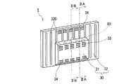
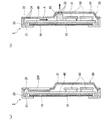
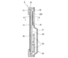
プラズマディスプレイ装置1は、フロントカバー20とバックカバー30を備えている。フロントカバー20とバックカバー30で囲まれる空間内には、画像を表示する表示パネルであるPDP10と、PDP10を前面で支持するシャーシ40と、シャーシ40の背面に取り付けられた、PDP10を駆動するため等の複数の回路基板50とが納められている。プラズマディスプレイ装置1は、画像表示方向から見たときに長方形の形状を有しており、一般に、長手方向が水平方向になり短手方向が鉛直方向になる姿勢(すなわち、PDP10が立てられた姿勢)で設置される。
The plasma display device 1 includes a
PDP10は、図3に示すように、前面パネル11と、背面パネル12と、それらの周辺部に形成された封止部材13とを有する。前面パネル11と背面パネル12は、それぞれの主面の縁部に配置された封止部材13により接着され、封止部材13の厚さの分だけ隔てられている。前面パネル11および背面パネル12は、ガラス基板などからなる。封止部材13により封止された前面パネル11と背面パネル12との間の密閉空間には、NeやXeなどの希ガスが注入されている。この密閉空間に電界を印加することにより、放電が起こり、発光する。
As shown in FIG. 3, the
PDP10の前面には、前面フィルタ14が貼り付けられている。前面フィルタ14は、外光反射を抑制する外光抑制フィルタや電磁波遮断フィルタ等、各種のフィルタで構成されている。
A
フロントカバー20は、プラズマディスプレイ装置1の前面と上下左右の側面を構成するような形状に形成されている。フロントカバー20における装置1の前面を構成する部分には、PDP10の画像表示領域が露出されるように開口が設けられている。フロントカバー20は、例えば厚み1mm程度のアルミニウム等の導電部材で構成されている。フロントカバー20は、前面フィルタ14の電磁波遮断フィルタと電気的に接続されている。また、フロントカバー20は、同様に導電部材で構成されるバックカバー30と接続されている。すなわち、フロントカバー20、バックカバー30、前面フィルタ14によって、PDP10を囲むシールド筐体を形成している。フロントカバー20は、PDP10の画像表示面の周囲を覆うエスカッション枠の役割も果たしている。
The
シャーシ40は、機械的剛性と熱伝導性の双方が良好なアルミニウム等の金属で構成されている。シャーシ40は、正面から見た形状および面積はPDP10とほぼ等しく、厚みが例えば1.0〜2.0mm程度である。図3に示すように、シャーシ40は、PDP10の背面パネル12における背面側の面と、熱伝導性を有する粘着シート41を介して全面的に接着されている。すなわち、表示パネルであるPDP10を前面で支持する。シャーシ40は、シャーシ40の周囲に配置された固定部材21を介して、フロントカバー20に固定されている。
The
粘着シート41は、正面から見た面積はPDP10とほぼ等しく長方形であり、厚みが例えば0.5〜2.0mm程度である。粘着シート41をPDP10とシャーシ40の間に介在させることによって、基本的にガラス基板から構成されるPDP10と、金属であるシャーシ40とを密着させ、PDP10からシャーシ40への熱伝導効果を高めている。このため、粘着シート41の材料としては、柔軟性と熱伝導性を兼ね備えたシリコン等が好適である。
The area of the pressure-sensitive
回路基板50は、PDP10を駆動する駆動回路基板や、PDP10に映像信号を送信するための信号処理回路基板等である。回路基板50は、ネジ等の固定部材によってシャーシ40の背面側に固定されている。本実施形態では、回路基板50は、シャーシ40の背面の中央下部に集中するように当該背面の所定領域上に配置されている。すなわち、所定領域は、シャーシ40の背面における中央下側領域である。なお、所定領域は、後述するバックカバー30の突出部31で覆われる。
The
バックカバー30は、シャーシ40および回路基板50を背面側から覆い、その周縁部においてフロントカバー20に接続されている。バックカバー30は、例えば厚み0.5mm程度のスチール等でできている。バックカバー30は、シャーシ40の背面における所定領域の外側を覆う縁部32、および縁部32の内側でシャーシ40と反対側に突出し、回路基板50を収容する突出部31を有する。ここで、バックカバー30の縁部32に対応する部分のプラズマディスプレイ装置1の厚みは例えば約1cmである。また、バックカバー30の突出部31に対応する部分のプラズマディスプレイ装置1の厚みは例えば約5cmである。
The
バックカバー30の縁部32には、特定方向に延びる複数の絞り部が設けられている。本実施形態では、各絞り部は、シャーシ40側に窪む凹部320である。凹部320は、突出部31の上方および側方に、鉛直方向に延びかつ水平方向に並ぶように設けられている。凹部320は、例えば深さ2〜5mm程度、幅10〜15mm程度である。凹部320は、平面状に形成された縁部32を絞り加工等で凹ませることによって形成することが出来る。本実施の形態においては、凹部320は、水平方向に等間隔で10箇所、具体的には突出部31の上方6箇所とその両側2箇所ずつ形成されている。
The
凹部320の長さは、特に限定されるものではなく、適宜選定可能である。本実施形態では、突出部31の上方に位置する凹部320も側方に位置する凹部320も、その位置の縁部32の高さよりも僅かに短い程度の長さを有している。
The length of the recessed
突出部31の内側には、複数のファン60が配設されている。ファン60は、図示しない取付け部材を介してシャーシ40に取付けられている。縁部32の上部には、凹部320同士の間に位置するように吸気孔34が設けられており、突出部31の上部には、凹部320同士の間に対応する位置に排気孔33が設けられている。さらに、本実施形態では、突出部31の下部にも吸気孔34が設けられている。そして、ファン60が稼働すると、シャーシ40とバックカバー50との間に吸気孔34から排気孔33へ向かう空気の流れが生じ、シャーシ40とバックカバー30で挟まれた空間の空気が排気孔33から外部に排出される。
A plurality of
なお、吸気孔34および排気孔33は、図示した位置に設けられている必要はない。例えば、バックカバー30の縁部32の外周縁部が前方に折り曲げられている場合は、その折り曲げられた部分に吸気孔34が設けられていてもよい。また、吸気孔34および排気孔33は、突出部31におけるシャーシ40と対向する主壁ではなく、その主壁の周縁部からシャーシ40側に広がりながら延びる周壁に設けられていてもよい。
The intake holes 34 and the exhaust holes 33 do not need to be provided at the illustrated positions. For example, when the outer peripheral edge portion of the
本実施の形態では、ファン60として遠心ファンが採用されており、突出部31内の上部領域に、排気孔33に向かって真っ直ぐに送風するように、水平方向に等間隔で5個設けられている。より詳しくは、ファン60は、バックカバー30における凹部320同士の間に対応する位置に配置されている。すなわち、5個のファン60は、縁部32に設けられた凹部320のうち、突出部31の上方に位置する凹部320の間に位置する様に設けられている。
In the present embodiment, a centrifugal fan is employed as the
以上、本実施の形態に係るプラズマディスプレイ装置1の構成について説明した。次に、プラズマディスプレイ装置1の作用について説明する。 The configuration of the plasma display apparatus 1 according to the present embodiment has been described above. Next, the operation of the plasma display device 1 will be described.
上述したとおり、プラズマディスプレイ装置1は、その上部と左右部にバックカバー30の縁部32に対応する厚みの薄い部分を有している。一般的に、プラズマディスプレイ装置1の背面側(バックカバー30側)は、壁面等に向かうように配置される。そのため、表示面側から見た場合に視界に入りやすい上部と左右部の厚みを薄くすることにより、視覚的に薄く見える効果が得られる。
As described above, the plasma display device 1 has thin portions corresponding to the
しかしながら、単に厚みの薄い部分を設けるだけでは、プラズマディスプレイ装置の強度が低下する。本実施の形態においては、バックカバー30の縁部32に、複数の凹部320が設けられている。この凹部320を設けることにより、バックカバー30の応力に対する変形を抑制し、強度を高めることが出来る。これにより、プラズマディスプレイ装置1の薄い部分の強度が向上し、落下や装置への外力付加による表示パネル破損等を防止することができる。
However, simply providing a thin portion reduces the strength of the plasma display device. In the present embodiment, a plurality of
また、本実施の形態においては、凹部320は、プラズマディスプレイ装置1の縦方向、すなわち鉛直方向に延在するように設けられている。このため、シャーシ40とバックカバー30とで挟まれる空間は、凹部320によって区画される。これにより、鉛直方向の空気の流路が形成される。ここで、ファン60は、バックカバー30における凹部320同士の間、つまり上述の空気の流路に対応して設けられている。このような構成により、PDP10から発生してシャーシ40に伝達される熱を、ファン60が効率的に放熱することが出来る。具体的には、図2(b)に矢印Aで示すような流路を空気が流れ、その空気が排気孔33を通じて排出されることで放熱される。もちろんファン60は、突出部31の下部に設けられた吸気孔34からの吸気により、突出部31内の回路基板50等から発生する熱に対しても放熱効果を有する。
Further, in the present embodiment, the
なお、本実施の形態において、突出部31は、バックカバー30の中央下側部分に形成したが、これに限られない。縁部32を下側部分にも形成し、突出部31を中央部分に形成してもよい。このようにすることで、壁掛け使用など下側部分も見えるような場合においても視覚的に薄く見せることが出来る。
In addition, in this Embodiment, although the
また、本実施の形態において、凹部320を10箇所、ファンを5個の構成としたが、個数はこれに限られず、適宜選択が可能である。また、凹部320の長さ、厚み(深さ)、幅なども適宜選択が可能であり、同一の装置内で様々な形の凹部320を形成してもよい。
In this embodiment, the number of
(実施の形態2)
次に、本発明の実施の形態2について、図4および図5を用いて説明する。実施の形態2は、凹部320がシャーシ40の背面に接触している点で実施の形態1と異なる。その他の部分は実施の形態1と同様の構成であり、その説明を省略する。
(Embodiment 2)
Next, Embodiment 2 of the present invention will be described with reference to FIGS. 4 and 5. FIG. The second embodiment is different from the first embodiment in that the
図4は、実施の形態2に係るプラズマディスプレイ装置2における、凹部320を含む断面図であり、実施の形態1における図2(a)に対応している。
FIG. 4 is a cross-sectional view including the
プラズマディスプレイ装置2は、バックカバー30の縁部32に設けられた凹部320と、シャーシ40の背面とが、熱伝導性を有する伝熱シート70を介して接触している。伝熱シート70を構成する材料としては、例えば、シリコン、アクリルなどを用いることが出来る。
In the plasma display device 2, the
伝熱シート70は、凹部320と同程度の長さおよび幅を有する短冊状であり、図5に示すように、各凹部320と対応する位置に配置されている。すなわち、各凹部320は、全長に亘って伝熱シート70を介してシャーシ40の背面に接触している。
The
ここで、PDP10の放熱の必要性について説明する。PDP10は、ガス放電を利用して画像を表示するという動作原理から高温になりやすい。そして、仮にPDP10の放熱が不十分で限界以上の高温になると、PDP10内部に形成されている電極の電気容量が変化して正常な放電が行われなくなるなどの弊害が生じる。このため、PDP10を所定の温度(一例として、70〜80℃)以下に保つ必要がある。特に、バックカバー30に縁部32を構成して自装置の周辺部分が薄くなるような構成においては、シャーシ40の背面側に放熱部材を追加することも困難であり、放熱性が低くなる。
Here, the necessity of heat dissipation of the
本実施の形態においては、上述したような伝熱シート70を用いることで、PDP10からシャーシ40に伝わった熱を熱伝導によりバックカバー30に伝えることが出来る。すなわち、PDP10に対する放熱効果をより高めることが出来る。
In the present embodiment, by using the
なお、本実施の形態では、凹部320とシャーシ40の背面とを伝熱シート70を介して接触させたが、それらを直接接触させてもよいし、他の熱伝導部材(例えば、ネジ)を介して接触させてもよい。このような接触構造であれば、低コストで実現することが出来る。また、凹部320とシャーシ40の背面とを接触させる熱伝導部材として、バネ部材等を用いてもよい。要するに、熱伝導させることが出来ればどのような接触構造も採用可能である。伝熱シート70を用いた場合には、容易に、薄く、広く接触させることが出来るため、製造工数や放熱効果の観点で有利である。
In the present embodiment, the
(その他の実施形態)
前記実施形態では、鉛直方向に延びる凹部320が突出部31の側方にも設けられていたが、突出部31の側方では、凹部320は、斜め方向または水平方向に延びていてもよい。あるいは、突出部31の側方では、凹部320を省略してもよい。すなわち、凹部320は、少なくとも突出部31の上方に、鉛直方向に延びかつ水平方向に並ぶように設けられていることが好ましい。
(Other embodiments)
In the embodiment, the recessed
また、凹部320は、必ずしも互いに平行に設けられている必要はなく、例えば、突出部31から放射状に広がるように設けられていてもよい。
Moreover, the recessed
さらに、特定方向に延びる絞り部は、シャーシ40側に窪む凹部である必要はなく、シャーシ40と反対側に突出する凸部であってもよい。
Further, the throttle portion extending in the specific direction does not have to be a concave portion that is recessed toward the
また、バックカバー30は、その上に導電膜が形成された樹脂成型品で構成することも可能である。すなわち、本発明の「絞り部」は、金属板を絞り加工するものに限られず、予めその形状に成型されたものであってもよい。
Moreover, the
本発明は、薄型のプラズマディスプレイ装置等の画像表示装置に好適である。 The present invention is suitable for an image display device such as a thin plasma display device.
1,2,3 プラズマディスプレイ装置(画像表示装置)
10,100 PDP(表示パネル)
11 前面パネル
12 背面パネル
13 封止部材
14 前面フィルタ
20,200 フロントカバー
21 固定部材
30,300 バックカバー
31 突出部
32 縁部
33 排気孔
34 吸気孔
40,400 シャーシ
41 粘着シート
50,500 回路基板
60 ファン
70 伝熱シート(熱伝導部材)
320 凹部(絞り部)
1,2,3 Plasma display device (image display device)
10,100 PDP (display panel)
DESCRIPTION OF
320 Concave part
Claims (4)
前記表示パネルを前面で支持するシャーシと、
前記シャーシの背面の所定領域上に配置された回路基板と、
前記シャーシの背面における前記所定領域の外側を覆う縁部、および前記縁部の内側で前記シャーシと反対側に突出し、前記回路基板を収容する突出部を有するバックカバーと、を備え、
前記縁部は、特定方向に延びる複数の絞り部を有し、
前記複数の絞り部のそれぞれは、前記シャーシ側に窪む凹部であり、
前記凹部は、前記シャーシの背面と直接的にまたは熱伝導部材を介して接触している、
画像表示装置。 A display panel for displaying images,
A chassis that supports the display panel on the front surface;
A circuit board disposed on a predetermined area of the back surface of the chassis;
An edge that covers the outside of the predetermined area on the back surface of the chassis, and a back cover that protrudes to the opposite side of the chassis inside the edge and has a protrusion that accommodates the circuit board.
The edges may have a plurality of throttle portions extending in a specific direction,
Each of the plurality of throttle portions is a concave portion recessed toward the chassis side,
The recess, that in contact through the back and directly or heat conduction member of said chassis,
Image display device.
前記凹部は、少なくとも前記突出部の上方に、鉛直方向に延びかつ水平方向に並ぶように設けられている、請求項1に記載の画像表示装置。 The image display device is installed in a posture in which the display panel is erected,
The image display device according to claim 1 , wherein the recess is provided so as to extend in a vertical direction and to be aligned in a horizontal direction at least above the protrusion.
前記突出部の内側には、前記シャーシと前記バックカバーとの間に前記吸気孔から前記排気孔へ向かう空気の流れを生じさせる複数のファンが配設されている、請求項2に記載の画像表示装置。 The edge portion is provided with an intake hole, and the protrusion portion is provided with an exhaust hole.
3. The image according to claim 2 , wherein a plurality of fans that generate an air flow from the intake hole toward the exhaust hole are disposed between the chassis and the back cover inside the protrusion. 4. Display device.
Priority Applications (1)
| Application Number | Priority Date | Filing Date | Title |
|---|---|---|---|
| JP2010182177A JP5073795B2 (en) | 2009-09-17 | 2010-08-17 | Image display device |
Applications Claiming Priority (3)
| Application Number | Priority Date | Filing Date | Title |
|---|---|---|---|
| JP2009215341 | 2009-09-17 | ||
| JP2009215341 | 2009-09-17 | ||
| JP2010182177A JP5073795B2 (en) | 2009-09-17 | 2010-08-17 | Image display device |
Publications (2)
| Publication Number | Publication Date |
|---|---|
| JP2011085903A JP2011085903A (en) | 2011-04-28 |
| JP5073795B2 true JP5073795B2 (en) | 2012-11-14 |
Family
ID=43730202
Family Applications (1)
| Application Number | Title | Priority Date | Filing Date |
|---|---|---|---|
| JP2010182177A Expired - Fee Related JP5073795B2 (en) | 2009-09-17 | 2010-08-17 | Image display device |
Country Status (2)
| Country | Link |
|---|---|
| US (1) | US20110063532A1 (en) |
| JP (1) | JP5073795B2 (en) |
Families Citing this family (9)
| Publication number | Priority date | Publication date | Assignee | Title |
|---|---|---|---|---|
| KR101237721B1 (en) | 2011-08-23 | 2013-02-26 | (주)크로스오버존 | Case for flat pannel display |
| JP5159933B1 (en) * | 2011-09-01 | 2013-03-13 | 株式会社東芝 | TV, electronics |
| CN102831829B (en) * | 2012-08-27 | 2015-05-06 | 深圳市华星光电技术有限公司 | Display device |
| CN102831825A (en) * | 2012-08-27 | 2012-12-19 | 深圳市华星光电技术有限公司 | Display device |
| CN102831830B (en) * | 2012-08-27 | 2015-05-06 | 深圳市华星光电技术有限公司 | Display device |
| CN102831828A (en) * | 2012-08-27 | 2012-12-19 | 深圳市华星光电技术有限公司 | Display device |
| JP2014071368A (en) * | 2012-09-28 | 2014-04-21 | Sharp Corp | Display device and television using the display device |
| JP2014153672A (en) | 2013-02-13 | 2014-08-25 | Toshiba Corp | Electronic apparatus |
| JP6277374B2 (en) * | 2013-09-09 | 2018-02-14 | 株式会社Joled | Display device |
Family Cites Families (14)
| Publication number | Priority date | Publication date | Assignee | Title |
|---|---|---|---|---|
| JPH07210093A (en) * | 1994-01-26 | 1995-08-11 | Fujitsu General Ltd | Plasma display device |
| JPH11296094A (en) * | 1998-04-10 | 1999-10-29 | Matsushita Electric Ind Co Ltd | Heat radiating method of plasma display |
| JP2000347578A (en) * | 1999-06-01 | 2000-12-15 | Pioneer Electronic Corp | Cooling structure of plasma display |
| US6493440B2 (en) * | 2001-04-23 | 2002-12-10 | Gilbarco Inc. | Thermal management for a thin environmentally-sealed LCD display enclosure |
| KR100783609B1 (en) * | 2001-07-10 | 2007-12-07 | 삼성전자주식회사 | Liquid crystal display device |
| JP2003289191A (en) * | 2002-03-28 | 2003-10-10 | Denso Corp | Electronic control device |
| KR100490158B1 (en) * | 2002-12-14 | 2005-05-16 | 엘지전자 주식회사 | back cover structure of refrigeration fan |
| JP4333206B2 (en) * | 2003-04-25 | 2009-09-16 | パナソニック株式会社 | Display device structure |
| JP2006106272A (en) * | 2004-10-04 | 2006-04-20 | Sony Corp | Display apparatus |
| JP2006162641A (en) * | 2004-12-02 | 2006-06-22 | Matsushita Electric Ind Co Ltd | Plasma display apparatus |
| KR20060114533A (en) * | 2005-05-02 | 2006-11-07 | 삼성에스디아이 주식회사 | Structure for mounting flat display module and flat panel display module comprising the same |
| JP4622940B2 (en) * | 2006-06-23 | 2011-02-02 | 株式会社日立製作所 | Information processing device |
| US20080068807A1 (en) * | 2006-09-20 | 2008-03-20 | Sunonwealth Electric Machine Industry Co., Ltd. | Heat-dissipating device for back light source for flat panel display |
| US20090021126A1 (en) * | 2007-07-18 | 2009-01-22 | Datavan International Corp. | Display panel |
-
2010
- 2010-08-17 JP JP2010182177A patent/JP5073795B2/en not_active Expired - Fee Related
- 2010-09-15 US US12/882,959 patent/US20110063532A1/en not_active Abandoned
Also Published As
| Publication number | Publication date |
|---|---|
| US20110063532A1 (en) | 2011-03-17 |
| JP2011085903A (en) | 2011-04-28 |
Similar Documents
| Publication | Publication Date | Title |
|---|---|---|
| JP5073795B2 (en) | Image display device | |
| US7372700B2 (en) | Plasma display device | |
| US7447034B2 (en) | Chassis base assembly and flat panel display device having the same | |
| US8325471B2 (en) | Display device | |
| KR20050122517A (en) | Plasma display panel assembly | |
| JP2007248689A (en) | Image display | |
| JP2001183987A (en) | Cooling structure and display device using the same | |
| JP2010081280A (en) | Video display apparatus | |
| JP2006317906A (en) | Plasma display device | |
| JP2007219379A (en) | Plasma display device | |
| JP2005084270A (en) | Thin type display device | |
| JPH1165485A (en) | Video display device | |
| JPH11242442A (en) | Plasma display device | |
| JP2011180476A (en) | Image display device | |
| JP2000010493A (en) | Video display device | |
| JP2008033093A (en) | Plasma display apparatus | |
| JPH11338370A (en) | Video display device | |
| JP4317194B2 (en) | Chassis assembly and plasma display device including the same | |
| JP2007328281A (en) | Display apparatus | |
| JP4309706B2 (en) | Flat panel display | |
| JP2002156913A (en) | Gas discharge type display device | |
| JP2009265206A (en) | Liquid crystal display device | |
| JP2006065119A (en) | Flat type display device | |
| KR20060095602A (en) | Chassis base assembly and plasma display panel assembly using the same | |
| US8330894B2 (en) | Display device |
Legal Events
| Date | Code | Title | Description |
|---|---|---|---|
| A977 | Report on retrieval |
Free format text: JAPANESE INTERMEDIATE CODE: A971007 Effective date: 20120418 |
|
| A131 | Notification of reasons for refusal |
Free format text: JAPANESE INTERMEDIATE CODE: A131 Effective date: 20120424 |
|
| A521 | Request for written amendment filed |
Free format text: JAPANESE INTERMEDIATE CODE: A523 Effective date: 20120606 |
|
| TRDD | Decision of grant or rejection written | ||
| A01 | Written decision to grant a patent or to grant a registration (utility model) |
Free format text: JAPANESE INTERMEDIATE CODE: A01 Effective date: 20120807 |
|
| A01 | Written decision to grant a patent or to grant a registration (utility model) |
Free format text: JAPANESE INTERMEDIATE CODE: A01 |
|
| A61 | First payment of annual fees (during grant procedure) |
Free format text: JAPANESE INTERMEDIATE CODE: A61 Effective date: 20120822 |
|
| R150 | Certificate of patent or registration of utility model |
Free format text: JAPANESE INTERMEDIATE CODE: R150 |
|
| FPAY | Renewal fee payment (event date is renewal date of database) |
Free format text: PAYMENT UNTIL: 20150831 Year of fee payment: 3 |
|
| LAPS | Cancellation because of no payment of annual fees |