JP5034541B2 - Piezoelectric vibrator, oscillator - Google Patents
Piezoelectric vibrator, oscillator Download PDFInfo
- Publication number
- JP5034541B2 JP5034541B2 JP2007034392A JP2007034392A JP5034541B2 JP 5034541 B2 JP5034541 B2 JP 5034541B2 JP 2007034392 A JP2007034392 A JP 2007034392A JP 2007034392 A JP2007034392 A JP 2007034392A JP 5034541 B2 JP5034541 B2 JP 5034541B2
- Authority
- JP
- Japan
- Prior art keywords
- thin film
- piezoelectric thin
- electrode
- vibrating arm
- piezoelectric
- Prior art date
- Legal status (The legal status is an assumption and is not a legal conclusion. Google has not performed a legal analysis and makes no representation as to the accuracy of the status listed.)
- Expired - Fee Related
Links
Images


Landscapes
- Oscillators With Electromechanical Resonators (AREA)
- Piezo-Electric Or Mechanical Vibrators, Or Delay Or Filter Circuits (AREA)
Description
本発明は、圧電体薄膜からなる圧電体薄膜素子を有する圧電振動子と、圧電振動子の製
造方法に関する。
The present invention relates to a piezoelectric vibrator having a piezoelectric thin film element made of a piezoelectric thin film and a method for manufacturing the piezoelectric vibrator.
一般に、電子機器等に搭載される時間標準やセンサとして低周波の圧電振動子が用いら
れている。電子機器の小型化に対応してこれらの圧電振動子の小型化が要求されている。
圧電振動子を単純に小型化していくとCI値が上昇しQ値が低下する。CI値を上昇さ
せない構造としては、振動片に圧電体膜を形成し、この圧電体膜を駆動する方法がある。
具体的には、シリコンからなる音叉の振動腕の主面上の中心線より内側及び外側に第1、
第2の電極と、これら電極上にそれぞれ設けられた第1、第2の圧電体膜と、これら圧電
体膜上のそれぞれに設けられた第3、第4の電極とを備え、第3、第4の電極に互いに逆
相の交流電圧を印加することにより音叉が屈曲振動する薄膜微小機械式共振子が提案され
ている(例えば、特許文献1参照)。
In general, a low-frequency piezoelectric vibrator is used as a time standard or sensor mounted on an electronic device or the like. In response to the downsizing of electronic equipment, downsizing of these piezoelectric vibrators is required.
When the piezoelectric vibrator is simply reduced in size, the CI value increases and the Q value decreases. As a structure that does not increase the CI value, there is a method in which a piezoelectric film is formed on a vibrating piece and this piezoelectric film is driven.
Specifically, the first, the inner side and the outer side of the center line on the main surface of the vibrating arm of a tuning fork made of silicon,
A second electrode, first and second piezoelectric films respectively provided on the electrodes, and third and fourth electrodes provided on the piezoelectric films, respectively, There has been proposed a thin film micromechanical resonator in which a tuning fork bends and vibrates by applying AC voltages having opposite phases to a fourth electrode (see, for example, Patent Document 1).
上述した特許文献1では、圧電体膜を電極で挟み込んだ形態で電極に電圧を印加して音
叉を励振している。このような構造では、音叉を駆動する駆動力を得るために圧電体膜の
厚さを数μm程度にしなければならず、コンデンサ容量が大きくなり、常に信号を発生さ
せるクロック信号用途等では、消費電力が大きくなってしまうとういう課題を有している
。
In
また、圧電体膜を用いる振動子あるいは共振子の振動性能は、圧電体膜の結晶性が良好
なほどよく、成膜温度が高いほど良好な結晶性が得られる。しかしながら、単純に圧電体
膜をシリコン表面に形成する方法では圧電体膜が均一で良好な結晶性が得られず、また、
高温にする場合には、音叉や電極等の材質が制約を受けるというような課題もある。
The vibration performance of a vibrator or resonator using a piezoelectric film is better as the crystallinity of the piezoelectric film is better, and better crystallinity is obtained as the film formation temperature is higher. However, the method of simply forming the piezoelectric film on the silicon surface does not provide uniform and good crystallinity of the piezoelectric film,
In the case of a high temperature, there is a problem that materials such as tuning forks and electrodes are restricted.
本発明の目的は、小型で消費電力が小さく周波数温度変化量が小さい高精度の圧電振動
子と、良好な結晶性を有する圧電体薄膜を有する圧電振動子の製造方法を提供することで
ある。
An object of the present invention is to provide a high-accuracy piezoelectric vibrator that is small in size, consumes less power and has a small amount of frequency temperature change, and a method of manufacturing a piezoelectric vibrator having a piezoelectric thin film having good crystallinity.
本発明の圧電振動子は、基部と、該基部から平行に延在される少なくとも一対の振動腕と、前記一対の振動腕それぞれの主面または側面に互いに異極となる励振電極と、を有する圧電振動片と、前記一対の振動腕それぞれの対向する主面または側面の少なくとも一つの表面に設けられる圧電体薄膜と該圧電体薄膜の表面に形成される電極とを有する圧電体薄膜素子と、が備えられ、前記圧電振動片と前記圧電体薄膜素子とが直列接続されていることを特徴とする。また、ある実施形態では、基部と、前記基部から伸長する振動腕と、を有し、前記振動腕は、第1面と、該第1面に対向する第2面と、前記第1面の端部と前記第2面の端部とを連結する側面と、を有し、前記第1面および前記第2面には、前記振動腕の前記伸長する方向に第1電極が形成され、前記側面には、前記振動腕の前記伸長する方向に第2電極が形成され、前記第1面および前記第2面の少なくとも一方の面上には、圧電体層と該圧電体層上に形成された第3電極とを含む積層部が形成され、前記積層部は前記第1電極と並列に配置され、前記第1電極と前記第2電極とは極性が異なり、前記第1電極と前記第3電極とは極性が同じであることを特徴とする。また、前記振動腕は、第1振動腕および第2振動腕を備え、前記第1振動腕および前記第2振動腕は、前記基部から並列に伸長し、且つ電極配置が互いに同じであり、前記第1振動腕の前記第1電極と、前記第1振動腕の前記第3電極と、前記第2振動腕の前記第2電極と、を互いに接続し、前記第1振動腕の前記第2電極と、前記第2振動腕の前記第1電極と、前記第2振動腕の前記第3電極と、を互いに接続することを特徴とする。また、前記圧電振動子と、前記圧電振動子に接続される増幅回路と、を備えた発振器としても良い。
The piezoelectric vibrator of the present invention has a base, at least a pair of vibrating arms extending in parallel from the base, and excitation electrodes having different polarities on the main surface or side surfaces of each of the pair of vibrating arms. A piezoelectric thin film element comprising: a piezoelectric vibrating piece; a piezoelectric thin film provided on at least one surface of the opposing main surface or side surface of each of the pair of vibrating arms; and an electrode formed on the surface of the piezoelectric thin film; The piezoelectric vibrating piece and the piezoelectric thin film element are connected in series. Further, in one embodiment, a base includes a vibrating arm extending from the base, and the vibrating arm includes a first surface, a second surface facing the first surface, and the first surface. A first electrode is formed on the first surface and the second surface in the extending direction of the vibrating arm, and the side surface connecting the end portion and the end portion of the second surface. A second electrode is formed on a side surface in the extending direction of the vibrating arm, and is formed on at least one of the first surface and the second surface on the piezoelectric layer and the piezoelectric layer. A stacked portion including the third electrode, the stacked portion is disposed in parallel with the first electrode, the first electrode and the second electrode have different polarities, and the first electrode and the third electrode The electrode is characterized by the same polarity. The resonating arm includes a first resonating arm and a second resonating arm, the first resonating arm and the second resonating arm extending in parallel from the base, and having the same electrode arrangement, The first electrode of the first vibrating arm is connected to the first electrode of the first vibrating arm, the third electrode of the first vibrating arm, and the second electrode of the second vibrating arm. And the first electrode of the second vibrating arm and the third electrode of the second vibrating arm are connected to each other. Moreover, it is good also as an oscillator provided with the said piezoelectric vibrator and the amplifier circuit connected to the said piezoelectric vibrator.
この発明によれば、圧電振動片と圧電体薄膜からなる圧電体薄膜素子とを直列に接続し、圧電振動片と圧電体薄膜素子とを同一励振信号で励振することから、圧電振動片と圧電体薄膜素子とが相互に振動を補完し合うことによって、低周波領域において圧電振動子の小型化を実現できる。また、前記圧電振動子を用いれば、小型で且つ低消費電力の発振器を構成することができる。
According to the present invention, the piezoelectric vibrating piece and the piezoelectric thin film element made of the piezoelectric thin film are connected in series, and the piezoelectric vibrating piece and the piezoelectric thin film element are excited by the same excitation signal. The piezoelectric thin film element can be miniaturized in the low frequency region by mutually supplementing the body thin film element with vibration. If the piezoelectric vibrator is used, a small-sized and low power consumption oscillator can be configured.
また、圧電振動片と圧電体薄膜素子とを直列に接続していることから、圧電振動片と圧
電体薄膜素子との総合コンデンサ容量を小さくすることができ、このことから消費電力を
増加させずに、圧電振動子の小型化を図ることができる。
In addition, since the piezoelectric vibrating piece and the piezoelectric thin film element are connected in series, the total capacitor capacity of the piezoelectric vibrating piece and the piezoelectric thin film element can be reduced, and this does not increase power consumption. In addition, the piezoelectric vibrator can be reduced in size.
また、前記圧電体薄膜のコンデンサ容量が前記圧電振動片のコンデンサ容量よりも大き
いことが好ましい。
Moreover, it is preferable that the capacitor capacity of the piezoelectric thin film is larger than the capacitor capacity of the piezoelectric vibrating piece.
本発明では、圧電振動片と圧電体薄膜素子とを直列に接続している。ここで、圧電振動
辺のコンデンサ容量をCq,圧電体薄膜のコンデンサ容量をCzで表すと、圧電振動子の
コンデンサ容量Cは、1/C=1/Cq+1/Czで表される。ここで、Cz>Cqとし
、その差を十分大きくすれば、C≒Cqと考えることができる。このことから、圧電振動
子コンデンサ容量Cを小さくすることができ、消費電力を増加させずに、水晶振動子の小
型化を実現できる。
In the present invention, the piezoelectric vibrating piece and the piezoelectric thin film element are connected in series. Here, when the capacitor capacity of the piezoelectric vibration side is represented by Cq and the capacitor capacity of the piezoelectric thin film is represented by Cz, the capacitor capacity C of the piezoelectric vibrator is represented by 1 / C = 1 / Cq + 1 / Cz. Here, if Cz> Cq and the difference is sufficiently large, it can be considered that C≈Cq. Therefore, the piezoelectric vibrator capacitor capacitance C can be reduced, and the quartz vibrator can be downsized without increasing the power consumption.
また、前記圧電振動片が、水晶からなることが好ましい。 The piezoelectric vibrating piece is preferably made of quartz.
水晶からなる圧電振動片は周波数温度特性に優れているため、補完的に圧電体薄膜を用
いる構造であっても、水晶が本来有する優れた周波数温度特性を活用できる。
Since the piezoelectric vibrating piece made of quartz is excellent in frequency temperature characteristics, the excellent frequency temperature characteristics inherent in quartz can be utilized even in a structure using a piezoelectric thin film complementarily.
また、前記一対の振動腕が、水晶のY軸方向に沿って延在され、前記対向する主面の一
方が水晶のX軸方向に2分され、前記圧電体薄膜素子が、2分された主面の水晶の結晶軸
方向側に設けられていることが好ましい。
Further, the pair of vibrating arms extends along the Y-axis direction of the crystal, one of the opposed main surfaces is divided into two in the X-axis direction of the crystal, and the piezoelectric thin film element is divided into two The main surface is preferably provided on the crystal axis direction side of the crystal.
前述したように、圧電振動片と圧電体薄膜素子とを直列に接続し、圧電体薄膜素子を水
晶の結晶軸方向側に配設することにより、圧電振動片と圧電体薄膜素子の振動モードが一
致し、圧電振動片と圧電体薄膜素子とが相互に振動を補完し合うことができる。
As described above, by connecting the piezoelectric vibrating piece and the piezoelectric thin film element in series and disposing the piezoelectric thin film element on the crystal axis direction side of the crystal, the vibration mode of the piezoelectric vibrating piece and the piezoelectric thin film element can be changed. Accordingly, the piezoelectric vibrating piece and the piezoelectric thin film element can complement each other for vibration.
また、前記一対の振動腕が、水晶のY軸方向に沿って延在され、前記対向する主面の両
方が水晶のX軸方向に2分され、前記圧電体薄膜素子が、2分された前記対向する主面そ
れぞれの水晶の結晶軸方向側に設けられていることが好ましい。
In addition, the pair of vibrating arms extends along the Y-axis direction of the crystal, both of the opposing main surfaces are divided into two in the X-axis direction of the crystal, and the piezoelectric thin film element is divided into two. It is preferable that the opposing main surfaces are provided on the crystal axis direction side of the crystal.
圧電振動片の表裏両面に圧電体薄膜素子を設けることにより、圧電振動片と圧電体薄膜
素子とが相互により一層強く振動を補完し合うことができる。また、一方の主面(表裏面
のどちらか一方)に圧電体薄膜素子を設ける構造よりも振動バランスをとることができる
。
By providing the piezoelectric thin film elements on both the front and back surfaces of the piezoelectric vibrating piece, the piezoelectric vibrating piece and the piezoelectric thin film element can complement each other more strongly with each other. In addition, vibration balance can be achieved as compared with a structure in which a piezoelectric thin film element is provided on one main surface (either one of the front and back surfaces).
また、前記一対の振動腕が、水晶のY軸方向に沿って延在され、前記対向する主面の両
方が水晶のX軸方向に2分され、前記圧電体薄膜素子が、2分された前記対向する主面そ
れぞれの水晶の結晶軸方向に水晶の結晶軸方向側と、水晶の結晶軸方向とは反対側の側面
と、に設けられていることが好ましい。
In addition, the pair of vibrating arms extends along the Y-axis direction of the crystal, both of the opposing main surfaces are divided into two in the X-axis direction of the crystal, and the piezoelectric thin film element is divided into two. It is preferable that the opposing main surfaces are provided on the crystal axis direction side of the crystal in the crystal axis direction of the crystal and on the side surface opposite to the crystal axis direction of the crystal.
このようにすれば、水晶の厚さ方向(Z軸方向)にも圧電体薄膜素子を設けることによ
り、さらに強く相互に振動を補完し合うことができ、圧電振動子の振動効率を高めること
ができる。
In this way, by providing the piezoelectric thin film element also in the thickness direction (Z-axis direction) of the crystal, it is possible to more strongly complement each other and to increase the vibration efficiency of the piezoelectric vibrator. it can.
また、前記振動腕にバランス質量が付加されていることが好ましい。 Further, it is preferable that a balance mass is added to the vibrating arm.
振動腕の表面に圧電体薄膜素子を設けることにより、振動のバランスが僅かではあるが
くずれることが予測される。そこで、圧電体薄膜素子に対応したバランス質量を付加する
ことにより、振動腕の振動バランスをとり、高精度な振動特性を維持することができる。
By providing the piezoelectric thin film element on the surface of the vibrating arm, it is expected that the balance of vibration is slightly broken. Therefore, by adding a balance mass corresponding to the piezoelectric thin film element, it is possible to balance the vibration of the vibrating arm and maintain highly accurate vibration characteristics.
前記バランス質量が、前記圧電体薄膜と同材質で形成されていることが望ましい。 The balance mass is preferably formed of the same material as the piezoelectric thin film.
このようにすれば、バランス質量を圧電体薄膜と同じ工程で形成することができるので
、高精度のバランス質量を付加することができる。また、圧電体薄膜形成設備を使用する
ことが可能である。
In this way, since the balance mass can be formed in the same process as the piezoelectric thin film, a highly accurate balance mass can be added. Moreover, it is possible to use a piezoelectric thin film forming facility.
また、本発明の圧電振動子の製造方法は、圧電基板の表面に第1圧電体薄膜を形成する
工程と、前記第1圧電体薄膜を熱処理する工程と、熱処理された前記第1圧電体薄膜の表
面に、前記第1圧電体薄膜と同一材料の第2圧電体薄膜を積層して圧電体薄膜を形成する
工程と、を含むことを特徴とする。
The method for manufacturing a piezoelectric vibrator of the present invention includes a step of forming a first piezoelectric thin film on a surface of a piezoelectric substrate, a step of heat-treating the first piezoelectric thin film, and the heat-treated first piezoelectric thin film. Forming a piezoelectric thin film by laminating a second piezoelectric thin film of the same material as the first piezoelectric thin film on the surface of the first piezoelectric thin film.
圧電体薄膜を用いる振動子あるいは共振子の振動性能は、圧電体薄膜の結晶性が良好な
ほどよい。そこで、第1圧電体薄膜を熱処理し、前記第1圧電体薄膜の表面に、前記第1
圧電体薄膜と同一材料の第2圧電体薄膜を形成することにより、良好な結晶性が得られ、
優れた振動性能を得ることができる。
The vibration performance of a vibrator or resonator using a piezoelectric thin film is better as the crystallinity of the piezoelectric thin film is better. Therefore, the first piezoelectric thin film is heat-treated, and the first piezoelectric thin film is formed on the surface of the first piezoelectric thin film.
By forming the second piezoelectric thin film of the same material as the piezoelectric thin film, good crystallinity is obtained,
Excellent vibration performance can be obtained.
また、本発明の圧電振動子の製造方法は、圧電基板の表面にPtまたはTiの少なくと
も一方の金属薄膜を形成する工程と、前記金属薄膜の表面に圧電体薄膜を形成する工程と
、を含むことを特徴とする。
The method for manufacturing a piezoelectric vibrator of the present invention includes a step of forming at least one metal thin film of Pt or Ti on the surface of the piezoelectric substrate, and a step of forming a piezoelectric thin film on the surface of the metal thin film. It is characterized by that.
圧電基板の表面にPtまたはTiの金属膜を形成することで、圧電体薄膜の結晶性を高
めることができる。ここで、金属膜としては、PtまたはTiの一層でもよく、TiとP
tの積層構造としてもよい。なお、金属膜は、電気的にはフローティングである。
By forming a metal film of Pt or Ti on the surface of the piezoelectric substrate, the crystallinity of the piezoelectric thin film can be improved. Here, the metal film may be a single layer of Pt or Ti, and Ti and P
It is good also as a laminated structure of t. Note that the metal film is electrically floating.
以下、本発明の実施形態を図面に基づいて説明する。
図1〜図5は、本発明の実施形態1に係る圧電振動子と製造方法を示し、図7,8は実
施形態2、図9,10は実施形態3、図11は実施形態4を示している。なお、以下の説
明で参照する図は、図示の便宜上、部材ないし部分の縦横の縮尺は実際のものとは異なる
模式図である。
(実施形態1)
Hereinafter, embodiments of the present invention will be described with reference to the drawings.
1 to 5 show a piezoelectric vibrator and manufacturing method according to
(Embodiment 1)
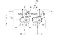
図1は、本発明の実施形態1に係る圧電振動子の構造を示す斜視図、図2は、図1のA
−A切断面を示す断面図及び各電極の接続説明図である。なお、本発明の圧電振動子の材
質としては、圧電性能を有するものであれば適合できるが、以下の実施形態では、圧電振
動子として水晶振動子を例示して説明する。図1、図2において、水晶振動子10は、水
晶振動片20の表面に複数の電極と圧電体薄膜素子100,101とを有して構成されて
いる。
FIG. 1 is a perspective view showing the structure of a piezoelectric vibrator according to
It is sectional drawing which shows -A cut surface, and connection explanatory drawing of each electrode. The material of the piezoelectric vibrator of the present invention can be applied as long as it has piezoelectric performance, but in the following embodiments, a quartz crystal vibrator will be described as an example of the piezoelectric vibrator. 1 and 2, the
水晶振動片20は、基部21の一辺から、Y軸方向に平行に延在された一対の振動腕3
0,40を有した音叉型振動子である。そして、基部21の振動腕30,40の延在方向
とは逆方向に支持部22が設けられている。振動腕30,40は、中心線C0に対して対
称形である。また、水晶振動片20は、結晶軸方向をX軸方向にして切り出されている。
The quartz
It is a tuning fork type vibrator having 0 and 40. A
振動腕30には、一方の主面(第1面)31(以降、表面31と表す)を2分し、振動腕30の中心線C1に対して結晶軸方向(振動腕の内側方向、または第1領域)に圧電体薄膜(圧電体層)71、外側方向(または、第2領域)に電極(第1電極)51が形成され、表面31に対向する主面(第2面)32(以降、裏面32と表す)に電極(第1電極)53が形成されている。なお、電極53は、圧電体薄膜71及び電極51に対向するように2分割する構成としてもよく、省略することもできる。また、振動腕30の外側側面33には電極(第2電極)52が、内側側面34には電極(第2電極)54が形成されている。さらに、圧電体薄膜71の表面には、電極(第3電極)55が形成されている。
The vibrating
振動腕40には、一方の主面(第1面)41(以降、表面41と表す)を2分し、振動腕40の中心線C2に対して結晶軸方向(振動腕の外側方向、または第2領域)に圧電体薄膜(圧電体層)72、内側方向(または、第1領域)に電極(第1電極)56が形成され、他方の主面(第2面)42(以降、裏面42と表す)に電極(第1電極)58が形成されている。なお、電極58は、圧電体薄膜71及び電極56に対向するように2分割する構成としてもよく、省略してもよい。また、振動腕40の外側側面43には電極(第2電極)59が、内側側面44には電極(第2電極)57が形成されている。さらに、圧電体薄膜72の表面には、電極(第3電極)60が形成されている。
In the vibrating
圧電体薄膜71,72の材料としては、ZnO、AlN、GaN、PZT(登録商標)
、KN、LN、LT等から選択することができ、本実施形態では、水晶よりも誘電率が大
きく、しかもその差が大きい材料、ヤング率が大きい材料、電気機械結合係数K2が大き
い材料を選択する。
As the material of the piezoelectric
, KN, LN, LT, and the like. In this embodiment, a material having a larger dielectric constant than quartz, a material having a large difference, a material having a large Young's modulus, and a material having a large electromechanical coupling coefficient K 2 are used. select.
電極55,51,53,57,59及び接続端子93は、接続電極91によって接続さ
れる。また、これらの電極とは互いに異極となる電極52,54,58,60,56及び
接続端子94は、接続電極92によって接続されている。そして、接続端子93,94に
それぞれ互いに逆相の交流電圧を印加することで、振動腕30,40がX軸方向に屈曲振
動する。従って、電極51〜60は、水晶振動片20の励振電極である。
The
図3は、水晶振動子を特定の振動モードで励振する発振回路に接続した状態を示す等価
回路図である。図3において、発振回路80は、増幅回路81と帰還回路82とを含んで
いる。
FIG. 3 is an equivalent circuit diagram showing a state in which the crystal resonator is connected to an oscillation circuit that excites in a specific vibration mode. In FIG. 3, the
増幅回路81は、増幅器83と帰還抵抗84とを含んで構成されている。帰還回路82
は、ドレイン抵抗85とコンデンサ86,87と水晶振動子10を含んで構成されている
。水晶振動子10は、水晶振動片20と圧電体薄膜素子100,101とが直列に接続さ
れている(図2も参照する)。
The
Includes a
ここで、増幅器83はCMOSインバータを用いることができる。このような構成によ
り、水晶振動片20と圧電体薄膜素子100,101とが同一振動モードで振動する発振
器80を形成することができる。
Here, the
続いて、本実施形態に係る水晶振動子の駆動について図面を参照して説明する。
図4、図5は、水晶振動子の駆動について模式的に示す説明図である。なお、図4、図
5は、図1のA−A切断面を表している。
図4(a)を参照して第1の状態を説明する。電極51,53,55,57,59には
マイナス(−)電位を印加し、電極52,54,56,58,60にはプラス(+)電位
を印加する。ここで、振動腕30,40の水晶の結晶軸方向を矢印Dで表し、圧電体薄膜
71,72の分極方向を矢印P0で表している。
Next, driving of the crystal resonator according to the present embodiment will be described with reference to the drawings.
4 and 5 are explanatory diagrams schematically showing driving of the crystal resonator. 4 and 5 show the AA cut plane of FIG.
The first state will be described with reference to FIG. A negative (−) potential is applied to the
まず、振動腕30について説明すると、圧電体薄膜71は、電極55と電極54によっ
て挟まれた圧電体薄膜素子100が形成された状態であり(水晶を一部介在する)、電極
55にマイナス電位、電極54にプラス電位を印加すると厚さ(Z軸)方向に縮み、幅(
X軸)方向及び長さ(Y軸)方向に伸びる。
First, the vibrating
X-axis) direction and length (Y-axis) direction.
従って、圧電体薄膜71は、水晶の結晶軸方向の偏った位置に設けられているために、
振動腕30を矢印F1方向に変位しようとする。振動腕30は、電極それぞれに電圧を印
加すると矢印E方向に電界が発生し、やはり矢印F1方向に変位しようとするため、振動
腕30は圧電体薄膜素子100と共に、矢印F1方向に変位する。
Therefore, the piezoelectric
An attempt is made to displace the vibrating
次に、振動腕40について説明する。圧電体薄膜72は、電極60と電極59によって
挟まれた圧電体薄膜素子101が形成された状態であり(水晶を一部介在する)、電極6
0にプラス電位、電極59にマイナス電位を印加すると厚さ(Z軸)方向に伸び、幅(X
軸)方向及び長さ(Y軸)方向に縮む。
Next, the vibrating
When a positive potential is applied to 0 and a negative potential is applied to the
(Axis) direction and length (Y axis) direction.
従って、圧電体薄膜72は、水晶の結晶軸方向の偏った位置に設けられているために、
振動腕40を矢印F2方向に変位しようとする。振動腕40は、電極それぞれに電圧を印
加すると矢印E方向に電界が発生し、やはり矢印F2方向に変位しようとするため、振動
腕40は圧電体薄膜素子101と共に、矢印F2方向に変位する。
このようにして、振動腕30,40は共に、図4(b)に示すように外側方向に変位す
る。
Therefore, since the piezoelectric
Attempts to displace the vibrating
In this way, the vibrating
次に、図5(a)を参照して第2の状態を説明する。第2の状態は、上述した第1の状
態に対して、各電極に逆相の電圧を印加した状態を示している。つまり、電極51,53
,55,57,59にはプラス(+)電位を印加し、電極52,54,56,58,60
にはマイナス(−)電位を印加する。
Next, the second state will be described with reference to FIG. The 2nd state has shown the state which applied the voltage of the reverse phase to each electrode with respect to the 1st state mentioned above. That is, the
, 55, 57, 59 are applied with a positive (+) potential, and the
A negative (-) potential is applied to.
まず、振動腕30について説明する。電極55にマイナス電位、電極54にプラス電位
を印加すると、圧電体薄膜71は厚さ(Z軸)方向に伸び、幅(X軸)方向及び長さ(Y
軸)方向に縮む。
First, the vibrating
Shrink in the (axis) direction.
従って、圧電体薄膜71は、振動腕30を矢印F3方向に変位しようとする。振動腕3
0は、電極それぞれに電圧を印加すると矢印E方向に電界が発生し、やはり矢印F3方向
に変位しようとするため、振動腕30は圧電体薄膜素子100と共に、矢印F3方向に変
位する。
Accordingly, the piezoelectric
In the case of 0, when a voltage is applied to each electrode, an electric field is generated in the direction of arrow E, and also tends to be displaced in the direction of arrow F 3 , so that the vibrating
次に、振動腕40について説明する。電極60にマイナス電位、電極59にプラス電位
を印加すると、圧電体薄膜72は厚さ(Z軸)方向に縮み、幅(X軸)方向及び長さ(Y
軸)方向に伸びる。従って、圧電体薄膜72は、矢印F4方向に変位しようとする。振動
腕40は、電極それぞれに電圧を印加すると矢印E方向に電界が発生し、やはり矢印F4
方向に変位しようとするため、振動腕40は圧電体薄膜素子101と共に、矢印F4方向
に変位する。
このようにして、振動腕30,40は、図5(b)に示すように内側方向に変位する。
Next, the vibrating
Axial) direction. Accordingly, the piezoelectric
In order to be displaced in the direction, the vibrating
In this way, the vibrating
上述した第1の状態と第2の状態を繰り返す(つまり、交流電圧を印加する)と振動腕
30,40は、X軸方向に屈曲振動を繰り返す。
When the first state and the second state described above are repeated (that is, an alternating voltage is applied), the vibrating
なお、上述した実施形態1では、圧電体薄膜素子100,101を振動腕30,40の
それぞれの表面31,41に形成する構造を例示したが、圧電体薄膜素子100,101
を、裏面32,42側に形成する構造としてもよい。この際、電極51と電極53、電極
56と電極58とを入れ替える構成とする。
In the first embodiment, the piezoelectric
It is good also as a structure formed in the back surfaces 32 and 42 side. At this time, the
なお、圧電体薄膜71,72は、その結晶性によって振動特性が影響される。そこで、
良好な結晶性を得るための製造方法について説明する。
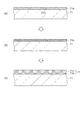
図6は、本実施形態に係る水晶振動子の第1の製造方法の一部を示す断面図である。図
示を省略するが、まず、大判の圧電基板としての水晶基板11(水晶ウエハと呼称するこ
とがある)に、フォトリソグラフィ技術によって複数の水晶振動片20を形成する。この
際、水晶振動片の基部21または支持部22を水晶基板11に接続しておく。
The vibration characteristics of the piezoelectric
A manufacturing method for obtaining good crystallinity will be described.
FIG. 6 is a cross-sectional view showing a part of the first manufacturing method of the crystal resonator according to the present embodiment. Although illustration is omitted, first, a plurality of
続いて、圧電体薄膜を形成する。なお、圧電体薄膜71と圧電体薄膜72は、同じ構成
であるので圧電体薄膜71を代表して説明する。図6(a)に示すように、振動腕30の
それぞれの表面31の所定位置に第1圧電体薄膜71aを形成する。第1圧電体薄膜71
aの形成方法は、RFスパッタリング法等のPVD(Physical Vapor D
eposition)法であてもよいし、CVD(Chemical Vapor De
position)法であってもよい。また、第1圧電体薄膜71aの厚さは、5nm〜
100nmが好ましい。
Subsequently, a piezoelectric thin film is formed. Since the piezoelectric
The formation method of a is PVD (Physical Vapor D) such as RF sputtering.
(eposition) method or CVD (Chemical Vapor De)
position) method. The thickness of the first piezoelectric
100 nm is preferred.
続いて、図6(b)に示すように、第1圧電体薄膜71aの熱処理を行い、熱処理後の
第1圧電体薄膜71bを形成する。熱処理は、ランプ加熱、レーザー光加熱であってもよ
いが、400℃以下での熱処理は、温度管理ができ温度を低温から上昇できる熱処理方法
が好ましい。具体的には、より安定した温度管理ができる熱処理炉、ホットプレート、真
空チャンバー中での熱処理が好ましい。熱処理後の第1圧電体薄膜71bは結晶化が進ん
だ状態である。
Subsequently, as shown in FIG. 6B, the first piezoelectric
続いて、図6(c)に示すように、熱処理後の第1圧電体薄膜71b上に第2圧電体薄
膜71cを形成する。第2圧電体薄膜71cは、結晶化が進んだ熱処理後の第1圧電体薄
膜71b上において結晶生長する材料であればどのような圧電体薄膜でもよいが、本実施
形態では、第1圧電体薄膜71aと同じ材料を採用している。
Subsequently, as shown in FIG. 6C, a second piezoelectric thin film 71c is formed on the heat-treated first piezoelectric
第2圧電体薄膜71cも、PVD法、CVD法等で形成することが可能で、その厚さは
数μmである。この第2圧電体薄膜71cは、熱処理後の第1圧電体薄膜71bを含めて
圧電体薄膜71となる。
The second piezoelectric thin film 71c can also be formed by a PVD method, a CVD method, or the like, and has a thickness of several μm. The second piezoelectric thin film 71c becomes the piezoelectric
このようにして圧電体薄膜71,72を形成した後、電極51〜60を形成する。圧電
体薄膜71,72それぞれの上面に形成する電極55,60も他の電極と同時形成しても
よいし、別工程で形成してもよい。
After the piezoelectric
電極51〜60を形成した後、水晶基板11をダイシング等で切断して、水晶振動子1
0を切り離し個片化する。
After the
Separate 0 and separate it.
続いて、本実施形態に係る水晶振動子の第2の製造方法について説明する。第2の製造
方法は、圧電体薄膜の製造方法のみが異なるため、圧電体薄膜の製造方法について説明す
る。図示は省略するが、図1,2,6を参照する。
まず、大判の水晶基板11(水晶ウエハ)にフォトリソグラフィ技術によって複数の水
晶振動片20を形成する。この際、水晶振動片の基部21または支持部22を水晶基板1
1に接続しておく。
Subsequently, a second manufacturing method of the crystal resonator according to the present embodiment will be described. Since the second manufacturing method is different only in the manufacturing method of the piezoelectric thin film, the manufacturing method of the piezoelectric thin film will be described. Although not shown, reference is made to FIGS.
First, a plurality of
Connect to 1.
水晶基板11の振動腕30,40のそれぞれの表面31,41の所定位置にPtまたは
Tiの金属薄膜を形成する。これらの金属膜はスパッタリング法、蒸着法等で形成する。
これらの金属薄膜は、圧電体薄膜の結晶化を促進する機能を有する。
A Pt or Ti metal thin film is formed at predetermined positions on the
These metal thin films have a function of promoting crystallization of the piezoelectric thin film.
続いて、PtまたはTiからなる金属薄膜の表面に圧電体薄膜71,72を形成する。
圧電体薄膜71,72は、金属薄膜が存在するために良好な結晶性を有する。
Subsequently, piezoelectric
The piezoelectric
なお、圧電体薄膜71,72の材質は、結晶性において金属薄膜に対しての相性がある
。具体的には、金属薄膜を形成する構造では、圧電体薄膜71,72の材質としてZnO
,AlN、GaNがより好ましい。しかし、上述した第1の製造方法においては、圧電体
薄膜71の材質は結晶性ということでは特に限定されない。
The material of the piezoelectric
AlN and GaN are more preferable. However, in the first manufacturing method described above, the material of the piezoelectric
また、金属薄膜として、Tiの表面にさらにPtを積層する構造としてもよく、このよ
うにすれば、圧電体薄膜71,72と水晶振動片20との界面の密着性を向上させ、且つ
、良好な結晶性を得ることができる。
Further, the metal thin film may have a structure in which Pt is further laminated on the surface of Ti. In this way, the adhesion at the interface between the piezoelectric
従って、前述した実施形態1によれば、水晶振動片20と圧電体薄膜素子100,10
1とを直列に接続し、水晶振動片20と圧電体薄膜素子100,101とを同一励振信号
で励振し、水晶振動片20と圧電体薄膜素子100,101とが相互に振動を補完し合う
ことから、低周波領域において水晶振動子10の小型化を実現できる。
Therefore, according to the first embodiment described above, the quartz
1 are connected in series, and the
ここで、消費電力に影響を与える水晶振動子10のコンデンサ容量について考察する。
コンデンサ容量Cは、誘電体の面積S、厚さ(電極間距離)d、誘電率をとすれば、C=
ε・S/dで表される。圧電体薄膜71,72の誘電率εz、水晶の誘電率εqの関係は
、それぞれの材料をεz≫εq、圧電体薄膜71,72の厚さdzと水晶振動片20の厚
さdqの関係を、dq≫dzとなるように設定している。従って、水晶振動片20のコン
デンサ容量Cqと圧電体薄膜71,72のコンデンサ容量Czの関係は、Cz≫Cqとな
る。
Here, the capacitor capacity of the
Capacitor capacity C is expressed as C == dielectric area S, thickness (distance between electrodes) d, and dielectric constant.
It is expressed by ε · S / d. The relationship between the dielectric constant εz of the piezoelectric
本実施形態では、発振器80の等価回路において、水晶振動片20と圧電体薄膜素子1
00,101とを直列に接続している。従って、水晶振動子10のコンデンサ容量Cは、
1/C=1/Cq+1/Czで表される。ここで、Cz≫Cqとしているため、C≒Cq
と考えることができる。このことから、水晶振動子10のコンデンサ容量を小さくするこ
とができ、消費電力を増加させずに、水晶振動子の小型化を実現できる。
In the present embodiment, in the equivalent circuit of the
00 and 101 are connected in series. Therefore, the capacitor capacity C of the
1 / C = 1 /
Can be considered. Therefore, the capacitor capacity of the
また、圧電体薄膜素子100,101の電気機械結合係数K2は、水晶振動片20の電
気機械結合係数よりも大きい。性能指数MはM≒K2・Qで表すことができ、圧電体薄膜
素子100,101の電気機械結合係数(K2で表される)を水晶よりも大きくすること
で、圧電体薄膜素子100,101の性能指数Mが高くなる。従って、電気機械結合係数
が大きいほど振動しやすいので、薄い圧電体薄膜71,72により水晶振動片20の振動
を高効率化することができる。
Further, the electromechanical coupling coefficient K 2 of the piezoelectric
また、本実施形態では、圧電振動片として水晶を採用している。水晶は、周波数温度特
性に優れているため、補完的に圧電体薄膜71,72を備える構造であっても、水晶の良
好な周波数温度特性を活用できる。
In the present embodiment, quartz is used as the piezoelectric vibrating piece. Since quartz is excellent in frequency temperature characteristics, even if the piezoelectric
また、振動腕30,40が、水晶のY軸(機械軸)方向に沿って延在され、圧電体薄膜
71,72が、振動腕30,40それぞれの表面31,41または裏面32,42の一方
または両方のX軸(電気軸)方向に2分された結晶軸方向側に設けられている。そのため
に、振動腕30,40と圧電体薄膜素子100,101の振動モードが一致し、水晶振動
片20と圧電体薄膜素子100,101とが相互に振動を補完し合うことができる。
The vibrating
また、圧電体薄膜を用いる振動子あるいは共振子の振動性能は、圧電体薄膜の結晶性が
良好なほどよい。本実施形態の水晶振動子10の製造方法は、水晶基板11の表面に第1
圧電体薄膜71aを形成し、この第1圧電体薄膜71aを熱処理した後、熱処理された前
記第1圧電体薄膜71bの表面に、第1圧電体薄膜71aと同一材料の第2圧電体薄膜7
1cを形成して結晶性を改善している。第2圧電体薄膜71cは、本実施形態の圧電体薄
膜71に相当する。従って、良好な結晶性を有する圧電体薄膜71,72により、優れた
振動性能を得ることができる。
The vibration performance of a vibrator or resonator using a piezoelectric thin film is better as the crystallinity of the piezoelectric thin film is better. The manufacturing method of the
After the piezoelectric
The crystallinity is improved by forming 1c. The second piezoelectric thin film 71c corresponds to the piezoelectric
また、本発明の水晶振動子10の他の製造方法として、水晶基板11の表面にPtまた
はTiの少なくとも一方の金属薄膜を形成し、この金属薄膜の表面に圧電体薄膜71を形
成する方法がある。このような金属薄膜を形成することで、圧電体薄膜71,72の結晶
性を高めることができる。
(実施形態2)
As another method for manufacturing the
(Embodiment 2)
続いて、本発明の実施形態2について図面を参照して説明する。実施形態2は、前述し
た実施形態1に対して圧電体薄膜を振動腕の表裏両面に設けたことを特徴としている。従
って、実施形態1との相違部分を中心に説明し、同じ構成部位には同じ符号を附している
。
図7、図8は、実施形態2に係る水晶振動子を示す断面図(図1のA−A切断面に相当
する)である。図7、図8において、振動腕30の表面31には、幅方向(X軸方向)を
2分して、振動腕30の中心線C1に対して結晶軸方向(振動腕30の内側側面34方向
)に圧電体薄膜71、外側方向に電極51が形成されている。
Subsequently, Embodiment 2 of the present invention will be described with reference to the drawings. The second embodiment is characterized in that piezoelectric thin films are provided on both the front and back surfaces of the vibrating arm as compared with the first embodiment. Therefore, it demonstrates centering on a different part from
7 and 8 are cross-sectional views (corresponding to the AA cut plane in FIG. 1) showing the crystal resonator according to the second embodiment. 7 and 8, the
また、振動腕30の裏面32には、圧電体薄膜71に対向して圧電体薄膜73が形成さ
れ、電極51に対向して電極53が形成されている。さらに、振動腕30の外側側面33
には電極52が、内側側面34には電極54が形成され、圧電体薄膜71の表面には、電
極55、圧電体薄膜73の表面には電極61が形成されている。従って、圧電体薄膜73
は、電極61,54によって挟まれた圧電体薄膜素子102を構成する。
Further, a piezoelectric
The
Constitutes the piezoelectric
一方、振動腕40の表面41には、幅方向(X軸方向)を2分して、振動腕40の中心
線C2に対して結晶軸方向(振動腕40の外側側面43方向)に圧電体薄膜72、内側方
向に電極56が形成されている。
On the other hand, on the
また、振動腕40の裏面42には、圧電体薄膜72に対向して圧電体薄膜74が形成さ
れ、電極56に対向して電極58が形成されている。さらに、振動腕40の外側側面43
には電極59が、内側側面44には電極57が形成され、圧電体薄膜72の表面には、電
極60、圧電体薄膜74の表面には電極62が形成されている。従って、圧電体薄膜74
は、電極62,59によって挟まれた圧電体薄膜素子103を構成する。
なお、圧電体薄膜71〜74は実施形態1と同様な材料としての条件を満たし、厚さ、
平面形状も同じとする。
Further, on the
The
Constitutes the piezoelectric
The piezoelectric
The planar shape is the same.
電極55,51,53,61,57,59及び接続端子93は、接続電極91によって
接続される。また、電極52,54,58,62,60,56及び接続端子94は、接続
電極92によって接続されている。そして、接続端子93,94にそれぞれ逆相の交流電
圧を印加することで、振動腕30,40が屈曲振動する。従って、電極51〜62は、水
晶振動片20の励振電極である。
The
上述したように構成される水晶振動子10は、発振器の等価回路において、図3に示し
たときと同じように、水晶振動片20と圧電体薄膜素子100〜103とは直列に接続さ
れている。
In the
続いて、本実施形態に係る水晶振動子の駆動について図面を参照して説明する。
図8は、水晶振動子の駆動について第1の状態を模式的に示す説明図である。電極51
,53,55,57,59,61にはマイナス(−)電位を印加し、電極52,54,5
8,62,60,56にはプラス(+)電位を印加する。ここで、振動腕30,40の水
晶の結晶軸方向を矢印Dで表し、圧電体薄膜71〜74の分極方向を矢印P0で表してい
る。
Next, driving of the crystal resonator according to the present embodiment will be described with reference to the drawings.
FIG. 8 is an explanatory diagram schematically showing a first state of driving of the crystal unit.
, 53, 55, 57, 59, 61 are applied with a negative (−) potential, and the
A positive (+) potential is applied to 8, 62, 60, and 56. Here, the crystal axis direction of the quartz crystal of the vibrating
まず、振動腕30について説明すると、圧電体薄膜71,73は、電極55,61にマ
イナス電位、電極54にプラス電位を印加すると厚さ(Z軸)方向に縮み、幅(X軸)方
向及び長さ(Y軸)方向に伸びる。
First, the vibrating
また、圧電体薄膜73は、電極61にマイナス電位、電極54にプラス電位を印加する
と厚さ(Z軸)方向に縮み、幅(X軸)方向及び長さ(Y軸)方向に伸びる。
The piezoelectric
従って、圧電体薄膜71,73は、振動腕30の水晶の結晶軸方向に偏った位置に設け
られていることから、それぞれ同じように振動腕30を矢印F1方向に変位しようとする
。振動腕30は、電極それぞれに電圧を印加すると矢印E方向に電界が発生し、やはり矢
印F1方向に変位しようとするため、振動腕30は圧電体薄膜素子100,102と共に
、矢印F1方向に変位する。
Therefore, the piezoelectric
次に、振動腕40について説明する。圧電体薄膜72は、電極60にプラス電位、電極
59にマイナス電位を印加すると厚さ(Z軸)方向に伸び、幅(X軸)方向及び長さ(Y
軸)方向に縮む。
Next, the vibrating
Shrink in the (axis) direction.
また、圧電体薄膜74は、電極59にマイナス電位、電極62にプラス電位を印加する
と厚さ(Z軸)方向に伸び、幅(X軸)方向及び長さ(Y軸)方向に縮む。
Further, when a negative potential is applied to the
従って、圧電体薄膜72,74は、振動腕40の水晶の結晶軸方向に偏った位置に設け
られていることから、それぞれ同じように振動腕40を矢印F2方向に変位しようとする
。振動腕40は、電極それぞれに電圧を印加すると矢印E方向に電界が発生し、やはり矢
印F2方向に変位しようとするため、振動腕40は圧電体薄膜素子101,103と共に
、矢印F2方向に変位する。
このようにして、振動腕30,40は、図8(b)に示すように外側方向(図中、実線
で表す矢印方向)に変位する。
Accordingly, since the piezoelectric
In this way, the vibrating
次に、前述した第1の状態に対して各電極に逆相の電位を印加した第2の状態について
説明する。図示は省略するが、第2の状態では、電極52,54,58,62,60,5
6にはマイナス電位、電極51,53,61,55,57,59にはプラス電位の電圧を
印加する。こうすることで、圧電体薄膜71〜74の伸縮方向が第1の状態(図8(a)
参照)とは逆方向となり、振動腕30,40は図8(b)に破線で表す矢印方向に変位す
る。
従って、接続端子93,94に交流電圧を印加することで、振動腕30,40は屈曲振
動を継続する。
Next, a second state in which a reverse-phase potential is applied to each electrode with respect to the first state described above will be described. Although illustration is omitted, in the second state, the
A negative potential is applied to 6 and a positive potential is applied to the
The vibrating
Therefore, by applying an alternating voltage to the
従って、上述したように、振動腕30,40の表裏両面の水晶の結晶軸方向の同じ位置
に圧電体薄膜71,73、及び圧電体薄膜72,74を設けることにより、水晶振動片2
0と圧電体薄膜素子100〜103とが、より一層強く相互に振動を補完し合うことがで
きる。また、一方の主面(表裏面のどちらか一方)に圧電体薄膜を形成する場合よりも振
動バランスをとることができ、捩れ等の不用振動を低減することができる。
(実施形態3)
Therefore, as described above, by providing the piezoelectric
0 and the piezoelectric
(Embodiment 3)
続いて、本発明の実施形態3について図面を参照して説明する。実施形態3は、前述し
た実施形態2に対して圧電体薄膜を振動腕の側面にも設けたことを特徴としている。従っ
て、実施形態2との相違部分を中心に説明し、同じ構成部位には同じ符号を附している。
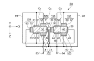
図9、図10は、実施形態3に係る水晶振動子を示す断面図(図1のA−A切断面に相
当する)である。図9、図10において、振動腕30には、表面31及び裏面32の両面
に圧電体薄膜71,73とそれらの表面それぞれに電極55,61が形成されている。
Subsequently, Embodiment 3 of the present invention will be described with reference to the drawings. The third embodiment is characterized in that a piezoelectric thin film is provided on the side surface of the vibrating arm as compared with the second embodiment. Therefore, it demonstrates centering on a different part from Embodiment 2, and attaches | subjects the same code | symbol to the same component.
9 and 10 are cross-sectional views (corresponding to the AA cut plane in FIG. 1) showing the crystal resonator according to the third embodiment. 9 and 10, the vibrating
そして、振動腕30の外側側面33に圧電体薄膜75が設けられ、その表面に電極63
が形成されている。
また、振動腕30の表面31には電極51、裏面32には電極51と対向して電極53
が形成され、内側側面34には電極54が形成されている。従って、圧電体薄膜75は、
電極63と電極51,53とによって挟まれた圧電体薄膜素子104を構成する。
A piezoelectric
Is formed.
Further, the
The
A piezoelectric
一方、振動腕40には、表面41及び裏面42の両面それぞれに圧電体薄膜72,74
と、それらの表面それぞれに電極60,62が設けられている。そして、振動腕40の内
側側面44に圧電体薄膜76が設けられ、その表面に電極64が形成されている。
また、振動腕40の表面41には電極56、裏面42には電極56と対向して電極58
が形成され、外側側面43には電極59が形成されている。従って、圧電体薄膜76は、
電極64と電極56,58とによって挟まれた圧電体薄膜素子105を構成する。
なお、圧電体薄膜75,76は、実施形態1,2と同様な材料が好ましく振動腕30,
40の内側方向に分極方向を矢印P0で表している。
On the other hand, the vibrating
Further, the
The
A piezoelectric
The piezoelectric
The direction of polarization is indicated by an arrow P 0 in the inner direction of 40.
電極55,51,53,61,64,59及び接続端子93は、接続電極91によって
接続される。また、電極63,54,58,62,60,56及び接続端子94は、接続
電極92によって接続されている。そして、接続端子93,94にそれぞれ逆相の交流電
圧を印加することで、振動腕30,40が屈曲振動する。従って、電極51〜64は、水
晶振動片20の励振電極である。
The
上述したように構成される水晶振動子10は、発振器の等価回路において、図3に示し
たときと同じように、水晶振動片20と圧電体薄膜素子100〜105とは直列に接続さ
れている。
In the
続いて、本実施形態に係る水晶振動子の駆動について図面を参照して説明する。
図10(a)は、水晶振動子の駆動について第1の状態を模式的に示す説明図である。
電極55,51,53,61,64,59にはマイナス(−)電位を印加し、電極63,
54,58,62,60,56にはプラス(+)電位を印加する。ここで、振動腕30,
40の水晶の結晶軸方向を矢印Dで表し、圧電体薄膜71〜76の分極方向を矢印P0で
表している。
Next, driving of the crystal resonator according to the present embodiment will be described with reference to the drawings.
FIG. 10A is an explanatory diagram schematically showing a first state for driving the crystal resonator.
A negative (−) potential is applied to the
A positive (+) potential is applied to 54, 58, 62, 60 and 56. Here, the vibrating
The crystal axis direction of 40 quartz is represented by an arrow D, and the polarization direction of the piezoelectric
まず、振動腕30について説明すると、圧電体薄膜71は、電極55と電極54によっ
て挟まれた圧電体薄膜素子100が形成された状態であり、電極55にマイナス電位、電
極54にプラス電位を印加すると厚さ(Z軸)方向に縮み、幅(X軸)方向及び長さ(Y
軸)方向に伸びる。
First, the vibrating
Axial) direction.
また、圧電体薄膜73は、電極61と電極54によって挟まれた圧電体薄膜素子102
が形成された状態であり、電極61にマイナス電位、電極54にプラス電位を印加すると
厚さ(Z軸)方向に縮み、幅(X軸)方向及び長さ(Y軸)方向に伸びる。
In addition, the piezoelectric
When a negative potential is applied to the
圧電体薄膜75は、電極63と電極51,53とによって挟まれた圧電体薄膜素子10
4が形成された状態であり、電極63にプラス電位、電極51,53にマイナス電位を印
加すると幅方向(Z軸方向)に伸び、厚さ方向(X軸方向)及び長さ方向(Y軸方向)に
縮む。
The piezoelectric
4 is formed, and when a positive potential is applied to the
従って、圧電体薄膜71,73,75は、それぞれ同じように振動腕30を矢印F1方
向に変位しようとする。振動腕30は、電極それぞれに電圧を印加すると矢印E方向に電
界が発生し、やはり矢印F1方向に変位しようとするため、振動腕30は圧電体薄膜素子
100,102,104と共に、矢印F1方向に変位する。
Therefore, the piezoelectric
次に、振動腕40について説明する。圧電体薄膜72は、電極60と電極59によって
挟まれた圧電体薄膜素子101が形成された状態であり、電極60にプラス電位、電極5
9にマイナス電位を印加すると厚さ(Z軸)方向に伸び、幅(X軸)方向及び長さ(Y軸
)方向に縮む。
Next, the vibrating
When a negative potential is applied to 9, the film expands in the thickness (Z-axis) direction and contracts in the width (X-axis) direction and length (Y-axis) direction.
また、圧電体薄膜74は、電極62と電極59によって挟まれた圧電体薄膜素子103
が形成された状態であり、電極59にマイナス電位、電極62にプラス電位を印加すると
厚さ(Z軸)方向に伸び、幅(X軸)方向及び長さ(Y軸)方向に縮む。
The piezoelectric
When a negative potential is applied to the
また、圧電体薄膜76は、電極64と電極56,58とによって挟まれた圧電体薄膜素
子105が形成された状態であり、電極64にマイナス電位、電極56,58にプラス電
位を印加すると幅方向(Z軸方向)に縮み、厚さ方向(X軸方向)及び長さ方向(Y軸方
向)に伸びる。
The piezoelectric
従って、圧電体薄膜素子101,103,105は、振動腕40を矢印F2方向に変位
しようとする。振動腕40は、電極それぞれに電圧を印加すると矢印E方向に電界が発生
し、やはり矢印F2方向に変位しようとするため、振動腕40は圧電体薄膜素子101,
103,105と共に、矢印F2方向に変位する。
このようにして、振動腕30,40は、図10(b)に示すように外側方向(図中、実
線で表す矢印方向)に変位する。
Therefore, the piezoelectric thin-
With 103 and 105, is displaced in the arrow F 2 direction.
In this way, the vibrating
次に、第1の状態に対して逆相の電位を各電極に印加した第2の状態について説明する
。図示は省略するが、第2の状態では、電極55,51,53,61,64,59にはプ
ラス電位、電極63,54,58,62,60,56にはマイナス電位の電圧を印加する
。こうすることで、圧電体薄膜71〜76の伸縮方向が第1の状態(図10(a)参照)
とは逆方向となり、振動腕30,40は図10(b)に破線で表す矢印方向に変位する。
従って、接続端子93,94に交流電圧を印加することで、振動腕30,40は屈曲振
動を継続する。
Next, a description will be given of a second state in which a potential opposite in phase to the first state is applied to each electrode. Although illustration is omitted, in the second state, a positive potential is applied to the
The vibrating
Therefore, by applying an alternating voltage to the
従って、上述した実施形態3によれば、水晶の側面にも圧電体薄膜素子104,105
を設けることにより、さらに強く相互に振動を補完し合うことができ、水晶振動子10の
振動効率を高めることができる。
(実施形態4)
Therefore, according to Embodiment 3 described above, the piezoelectric
By providing this, the vibrations can be complemented more strongly and the vibration efficiency of the
(Embodiment 4)
続いて、本発明の実施形態4について図面を参照して説明する。前述した実施形態1で
は圧電体薄膜素子100,101、実施形態2では圧電体薄膜素子100〜103、実施
形態3では圧電体薄膜素子100〜105をそれぞれ備えている。
Next, Embodiment 4 of the present invention will be described with reference to the drawings. The first embodiment includes the piezoelectric
しかしながら、圧電体薄膜素子を設けることにより、水晶振動片20の中心線C0に対
して振動腕30と振動腕40との質量バランス、あるいは、振動腕30,40それぞれの
中心線C1,C2に対する質量バランスがくずれることがある。そのことによって僅かであ
るが振動バランスがくずれることが考えられる。実施形態4では、そのような課題を解決
するためにバランス質量を付加することを特徴としている。
なお、実施形態1〜実施形態3と同じ部位には同じ符号を附している。
However, by providing the piezoelectric thin film element, the mass balance between the vibrating
In addition, the same code | symbol is attached | subjected to the site | part same as Embodiment 1-3.
図11(a)は、実施形態1(図2、参照)に対してバランス質量を付加した例を示し
ている。図11(a)において、振動腕30には、中心線C1に対して圧電体薄膜71と
対称となるバランス質量としての圧電体薄膜77aが設けられている。従って、付加され
た圧電体薄膜77aと電極51との積層体は、圧電体薄膜71と電極55との積層体と中
心線C1に対して対称となり、振動腕30内において質量バランスがとれる。
Fig.11 (a) has shown the example which added balance mass with respect to Embodiment 1 (refer FIG. 2). In FIG. 11 (a), the vibrating
振動腕40においても同様に、バランス質量としての圧電体薄膜77bを設けることに
より、付加された圧電体薄膜77bと電極56との積層体は、圧電体薄膜72と電極60
との積層体と中心線C2に対して対称となり、振動腕40内において質量バランスがとれ
ている。
Similarly, in the vibrating
Are symmetrical with respect to the center line C 2 and the mass line in the vibrating
このように、バランス質量として圧電体薄膜77a,77bを設けることにより、振動
腕30,40が、中心線C0に対して質量バランスがとれ、従って、振動バランスをとる
ことができる。
Thus, the piezoelectric
図11(b)は、実施形態2(図7、参照)に対してバランス質量を付加した例を示し
ている。実施形態2は、振動腕30,40それぞれの表裏両面に、圧電体薄膜71,73
、圧電体薄膜72,74が設けられている構造であるので、振動腕30には中心線C1に
対して圧電体薄膜71,73に対称なバランス質量としての圧電体薄膜77a,78aを
設け、振動腕40には中心線C2に対して圧電体薄膜72,74に対称なバランス質量と
しての圧電体薄膜77b,78bを設けている。
FIG.11 (b) has shown the example which added balance mass with respect to Embodiment 2 (refer FIG. 7). In the second embodiment, piezoelectric
Since a structure in which the piezoelectric
このようにバランス質量を設けることにより、振動腕30及び振動腕40内において質
量バランスがとれると共に、振動腕30と振動腕40との質量バランスがとれ、そのこと
により振動バランスがとれる。
By providing the balance mass in this way, the mass balance can be achieved in the vibrating
図11(c)は、実施形態3(図9、参照)に対してバランス質量を付加した例を示し
ている。実施形態3は、振動腕30の表裏両面と側面に圧電体薄膜71,73,75が設
けられている構造であるので、振動腕30には中心線C1に対して圧電体薄膜71,73
,75それぞれに対称なバランス質量としての圧電体薄膜77a,78a,79aを設け
る。また、振動腕40の表裏両面と側面に圧電体薄膜72,74,76が設けられている
構造であるので、振動腕40には中心線C2に対して圧電体薄膜72,74,76それぞ
れに対称なバランス質量としての圧電体薄膜77b,78b,79bを設けている。
FIG.11 (c) has shown the example which added balance mass with respect to Embodiment 3 (refer FIG. 9). Embodiment 3, since a structure in which the piezoelectric
, 75 are provided with piezoelectric
このようにバランス質量を設けることにより、振動腕30及び振動腕40内において質
量バランスがとれると共に、振動腕30と振動腕40との質量バランスがとれ、そのこと
により振動バランスがとれる。
By providing the balance mass in this way, the mass balance can be achieved in the vibrating
なお、本実施形態では、上述した図11(a)〜図11(c)において付加したバラン
ス質量としての圧電体薄膜77a,77b,78a,78b,79a,79bそれぞれを
、他の圧電体薄膜71〜76と同材質にしている。
In the present embodiment, each of the piezoelectric
従って、上述した実施形態4によれば、圧電体薄膜71〜76に対応したバランス質量
を付加することにより、振動腕30,40の振動バランスをとり、高精度な振動特性を得
ることができる。
また、バランス質量を圧電体薄膜と同材質で形成することにより、圧電体薄膜と同じ工
程でバランス質量を構成することができるので、高精度のバランス質量を付加することが
できる。さらに、圧電体薄膜形成設備を使用して形成することが可能である。
Therefore, according to Embodiment 4 described above, by adding a balance mass corresponding to the piezoelectric
Further, by forming the balance mass with the same material as that of the piezoelectric thin film, the balance mass can be configured in the same process as the piezoelectric thin film, so that a highly accurate balance mass can be added. Furthermore, it can be formed using a piezoelectric thin film forming facility.
なお、本発明は前述の実施の形態に限定されるものではなく、本発明の目的を達成でき
る範囲での変形、改良等は本発明に含まれるものである。
例えば、前述した実施形態1では、圧電体薄膜71,72を振動腕30,40のそれぞ
れの表面31,41に形成する構造、及び圧電体薄膜71,72を裏面32,42側に形
成する構造を説明したが、振動腕30の表面31に圧電体薄膜71を形成し、振動腕40
の裏面42に圧電体薄膜72を形成してもよく、その逆にしてもよい。
It should be noted that the present invention is not limited to the above-described embodiment, but includes modifications and improvements as long as the object of the present invention can be achieved.
For example, in the first embodiment described above, the piezoelectric
The piezoelectric
また、前述した実施形態4では、付加するバランス質量を圧電体薄膜と同材質を用いて
いるが、バランス質量は、中心線C0,C1,C2に対して質量バランス(つまり振動バラ
ンス)がとれれば、同材質でなくてもよく、圧電体でなくてもよい。
In the fourth embodiment described above, the balance mass to be added is the same material as that of the piezoelectric thin film, but the balance mass is a mass balance (ie, vibration balance) with respect to the center lines C 0 , C 1 , C 2 . If it can be removed, the material may not be the same, and the material may not be a piezoelectric body.
従って、前述した実施形態1〜実施形態4によれば、小型で消費電力が小さく高精度な
圧電振動子を提供することができる。
Therefore, according to the first to fourth embodiments described above, it is possible to provide a highly accurate piezoelectric vibrator that is small in size, low in power consumption.
10…水晶振動子、20…水晶振動片、21…基部、30,40…振動腕、31…振動
腕30の表面、32…振動腕30の裏面、33…振動腕30の外側側面、34…振動腕3
0の内側側面、41…振動腕40の表面、42…振動腕40の裏面、43…振動腕40の
外側側面、44…振動腕40の内側側面、55,60…電極、71,72…圧電体薄膜、
100,101…圧電体薄膜素子。
DESCRIPTION OF
0 inside surface, 41 ... surface of the vibrating
100, 101... Piezoelectric thin film element.
Claims (3)
前記基部から伸長する振動腕と、を有し、
前記振動腕は、第1面と、該第1面に対向する第2面と、前記第1面の端部と前記第2面の端部とを連結する側面と、を有し、
前記第1面および前記第2面には、前記振動腕の前記伸長する方向に第1電極が形成され、
前記側面には、前記振動腕の前記伸長する方向に第2電極が形成され、
前記第1面および前記第2面の少なくとも一方の面上には、圧電体層と該圧電体層上に形成された第3電極とを含む積層部が形成され、
前記積層部は前記第1電極と並列に配置され、
前記第1電極と前記第2電極とは極性が異なり、前記第1電極と前記第3電極とは極性が同じであることを特徴とする圧電振動子。 The base,
A vibrating arm extending from the base,
The resonating arm has a first surface, a second surface facing the first surface, and a side surface connecting the end portion of the first surface and the end portion of the second surface,
A first electrode is formed on the first surface and the second surface in the extending direction of the vibrating arm,
A second electrode is formed on the side surface in the extending direction of the vibrating arm,
A laminated portion including a piezoelectric layer and a third electrode formed on the piezoelectric layer is formed on at least one of the first surface and the second surface,
The stacked portion is arranged in parallel with the first electrode,
The piezoelectric vibrator according to claim 1, wherein the first electrode and the second electrode have different polarities, and the first electrode and the third electrode have the same polarity .
前記振動腕は、第1振動腕および第2振動腕を備え、 The vibrating arm includes a first vibrating arm and a second vibrating arm,
前記第1振動腕および前記第2振動腕は、前記基部から並列に伸長し、且つ電極配置が互いに同じであり、 The first vibrating arm and the second vibrating arm extend in parallel from the base and have the same electrode arrangement.
前記第1振動腕の前記第1電極と、前記第1振動腕の前記第3電極と、前記第2振動腕の前記第2電極と、を互いに接続し、 Connecting the first electrode of the first vibrating arm, the third electrode of the first vibrating arm, and the second electrode of the second vibrating arm;
前記第1振動腕の前記第2電極と、前記第2振動腕の前記第1電極と、前記第2振動腕の前記第3電極と、を互いに接続することを特徴とする圧電振動子。 The piezoelectric vibrator, wherein the second electrode of the first vibrating arm, the first electrode of the second vibrating arm, and the third electrode of the second vibrating arm are connected to each other.
Priority Applications (1)
| Application Number | Priority Date | Filing Date | Title |
|---|---|---|---|
| JP2007034392A JP5034541B2 (en) | 2007-02-15 | 2007-02-15 | Piezoelectric vibrator, oscillator |
Applications Claiming Priority (1)
| Application Number | Priority Date | Filing Date | Title |
|---|---|---|---|
| JP2007034392A JP5034541B2 (en) | 2007-02-15 | 2007-02-15 | Piezoelectric vibrator, oscillator |
Publications (3)
| Publication Number | Publication Date |
|---|---|
| JP2008199439A JP2008199439A (en) | 2008-08-28 |
| JP2008199439A5 JP2008199439A5 (en) | 2010-03-18 |
| JP5034541B2 true JP5034541B2 (en) | 2012-09-26 |
Family
ID=39757974
Family Applications (1)
| Application Number | Title | Priority Date | Filing Date |
|---|---|---|---|
| JP2007034392A Expired - Fee Related JP5034541B2 (en) | 2007-02-15 | 2007-02-15 | Piezoelectric vibrator, oscillator |
Country Status (1)
| Country | Link |
|---|---|
| JP (1) | JP5034541B2 (en) |
Family Cites Families (5)
| Publication number | Priority date | Publication date | Assignee | Title |
|---|---|---|---|---|
| JPS5549020A (en) * | 1978-10-04 | 1980-04-08 | Seiko Instr & Electronics Ltd | Piezoelectric vibrator |
| JPS5699929U (en) * | 1979-12-28 | 1981-08-06 | ||
| JP4434537B2 (en) * | 2001-08-27 | 2010-03-17 | パナソニック株式会社 | Piezoelectric functional parts |
| JP3972790B2 (en) * | 2001-11-27 | 2007-09-05 | 松下電器産業株式会社 | Thin film micromechanical resonator and thin film micromechanical resonator gyro |
| JP2005249646A (en) * | 2004-03-05 | 2005-09-15 | Matsushita Electric Ind Co Ltd | Tuning fork type oscillator for angular velocity sensor, angular velocity sensor using the oscillator, and automobile using the angular velocity sensor |
-
2007
- 2007-02-15 JP JP2007034392A patent/JP5034541B2/en not_active Expired - Fee Related
Also Published As
| Publication number | Publication date |
|---|---|
| JP2008199439A (en) | 2008-08-28 |
Similar Documents
| Publication | Publication Date | Title |
|---|---|---|
| US9866199B2 (en) | Vibrating device | |
| US8786166B2 (en) | Micromechanical resonator array and method for manufacturing thereof | |
| CN107005224B (en) | Temperature compensation plate resonator | |
| US9584093B2 (en) | Vibrating device | |
| US9071226B2 (en) | Micromechanical resonator and method for manufacturing thereof | |
| CN101847978B (en) | Flexural vibration piece and oscillator using the same | |
| US9905748B2 (en) | Vibrating device | |
| JP2018506930A5 (en) | ||
| CN102739179B (en) | Mems resonator and method of controlling the same | |
| WO2007088696A1 (en) | Piezoelectric oscillator | |
| JP5067486B2 (en) | Bending vibrator, bending vibrator, and piezoelectric device | |
| JP2009111623A (en) | Piezoelectric vibrating device | |
| JP2010226610A (en) | Bent vibrating piece and oscillator employing the same | |
| JP5034540B2 (en) | Piezoelectric vibrator, oscillator | |
| JP5034541B2 (en) | Piezoelectric vibrator, oscillator | |
| JP5168930B2 (en) | Piezoelectric vibrator, oscillator | |
| JP2007500478A (en) | Multilayer resonator and time base incorporating the resonator | |
| JPH10173476A (en) | Tuning fork piezoelectric oscillator | |
| JP2009100076A (en) | Piezoelectric vibrating reed | |
| JP2007240540A (en) | Thin-film micromechanical resonator gyro | |
| JP4930769B2 (en) | Oscillator | |
| JP2003273703A (en) | Quartz vibrator and its manufacturing method | |
| US20110127621A1 (en) | Electrostatic vibrator and electronic apparatus | |
| JP2008072156A (en) | Composite material vibrator | |
| JP2003229739A (en) | Quartz oscillator and its manufacturing method |
Legal Events
| Date | Code | Title | Description |
|---|---|---|---|
| A521 | Request for written amendment filed |
Free format text: JAPANESE INTERMEDIATE CODE: A523 Effective date: 20100128 |
|
| A621 | Written request for application examination |
Free format text: JAPANESE INTERMEDIATE CODE: A621 Effective date: 20100128 |
|
| A977 | Report on retrieval |
Free format text: JAPANESE INTERMEDIATE CODE: A971007 Effective date: 20120528 |
|
| TRDD | Decision of grant or rejection written | ||
| A01 | Written decision to grant a patent or to grant a registration (utility model) |
Free format text: JAPANESE INTERMEDIATE CODE: A01 Effective date: 20120605 |
|
| A01 | Written decision to grant a patent or to grant a registration (utility model) |
Free format text: JAPANESE INTERMEDIATE CODE: A01 |
|
| A61 | First payment of annual fees (during grant procedure) |
Free format text: JAPANESE INTERMEDIATE CODE: A61 Effective date: 20120618 |
|
| FPAY | Renewal fee payment (event date is renewal date of database) |
Free format text: PAYMENT UNTIL: 20150713 Year of fee payment: 3 |
|
| R150 | Certificate of patent or registration of utility model |
Free format text: JAPANESE INTERMEDIATE CODE: R150 |
|
| LAPS | Cancellation because of no payment of annual fees |