JP5034540B2 - Piezoelectric vibrator, oscillator - Google Patents
Piezoelectric vibrator, oscillator Download PDFInfo
- Publication number
- JP5034540B2 JP5034540B2 JP2007034391A JP2007034391A JP5034540B2 JP 5034540 B2 JP5034540 B2 JP 5034540B2 JP 2007034391 A JP2007034391 A JP 2007034391A JP 2007034391 A JP2007034391 A JP 2007034391A JP 5034540 B2 JP5034540 B2 JP 5034540B2
- Authority
- JP
- Japan
- Prior art keywords
- piezoelectric thin
- electrode
- thin film
- vibrating arm
- piezoelectric
- Prior art date
- Legal status (The legal status is an assumption and is not a legal conclusion. Google has not performed a legal analysis and makes no representation as to the accuracy of the status listed.)
- Expired - Fee Related
Links
Images


Landscapes
- Oscillators With Electromechanical Resonators (AREA)
- Piezo-Electric Or Mechanical Vibrators, Or Delay Or Filter Circuits (AREA)
Description
本発明は、圧電体薄膜と温度補償膜とを有する圧電振動子と、この圧電振動子の製造方
法に関する。
The present invention relates to a piezoelectric vibrator having a piezoelectric thin film and a temperature compensation film, and a method for manufacturing the piezoelectric vibrator.
一般に、電子機器等に搭載される時間標準やセンサとして低周波の圧電振動子が用いら
れている。電子機器の小型化に対応してこれらの圧電振動子の小型化が要求されている。
圧電振動子を単純に小型化していくとCI値が上昇しQ値が低下する。CI値を上昇さ
せない構造としては、振動片に圧電体膜を形成し、この圧電体膜を駆動する方法がある。
In general, a low-frequency piezoelectric vibrator is used as a time standard or sensor mounted on an electronic device or the like. In response to the downsizing of electronic equipment, downsizing of these piezoelectric vibrators is required.
When the piezoelectric vibrator is simply reduced in size, the CI value increases and the Q value decreases. As a structure that does not increase the CI value, there is a method in which a piezoelectric film is formed on a vibrating piece and this piezoelectric film is driven.
具体的には、シリコンからなる音叉の振動腕の主面上の中心線より内側及び外側に第1
、第2の電極と、これら電極上それぞれに設けられた第1、第2の圧電体膜と、これら圧
電体膜上のそれぞれに設けられた第3、第4の電極とを備え、第3、第4の電極に互いに
逆相の交流電圧を印加することにより音叉が屈曲振動する薄膜微小機械式共振子が提案さ
れている(例えば、特許文献1参照)。
Specifically, the first inner side and the outer side from the center line on the main surface of the vibrating arm of a tuning fork made of silicon.
A second electrode, first and second piezoelectric films provided on each of these electrodes, and third and fourth electrodes provided on each of these piezoelectric films, There has been proposed a thin film micromechanical resonator in which a tuning fork bends and vibrates by applying AC voltages having opposite phases to a fourth electrode (see, for example, Patent Document 1).
また、周波数温度特性がよい恒弾性金属材料に圧電体薄膜としてZnO薄膜を形成した
音叉型振動子というものも知られている(例えば、非特許文献1参照)。
There is also known a tuning fork vibrator in which a ZnO thin film is formed as a piezoelectric thin film on a constant elastic metal material having good frequency temperature characteristics (see, for example, Non-Patent Document 1).
上述した特許文献1や非特許文献1では、圧電体膜に電圧を印加して金属またはシリコ
ン等からなる音叉を励振している。このような構造では、音叉を駆動する駆動力を得るた
めに圧電体薄膜の厚さを数μm程度にしなければならず、コンデンサ容量が大きくなり、
常に信号を発生させるクロック信号用途等では、消費電力が大きくなってしまうという課
題を有している。
In
In clock signal applications that always generate signals, there is a problem that power consumption increases.
また、特許文献1や非特許文献1に例示されている圧電体薄膜は、ZnOやチタン酸ジ
ルコン酸塩等の圧電性材料であって、これらの圧電体材料は周波数温度変化量が大きい。
従って、金属またはシリコン、あるいは周波数温度変化量が小さい水晶に圧電体薄膜を付
加する構造が考えられる。しかしながら、圧電体薄膜が有する一次温度係数の影響により
周波数温度変化量が大きくなるという課題を有している。
Further, the piezoelectric thin films exemplified in
Therefore, a structure in which a piezoelectric thin film is added to metal, silicon, or quartz having a small frequency temperature change is conceivable. However, there is a problem that the amount of change in frequency temperature is increased due to the influence of the primary temperature coefficient of the piezoelectric thin film.
本発明の目的は、小型で消費電力が小さく周波数温度変化量が小さい高精度の圧電振動
子と、この圧電振動子の製造方法を提供することである。
An object of the present invention is to provide a highly accurate piezoelectric vibrator that is small in size, consumes less power and has a small amount of frequency temperature change, and a method for manufacturing the piezoelectric vibrator.
本発明の圧電振動子は、基部と、該基部から平行に延在される少なくとも一対の振動腕と、前記一対の振動腕それぞれの対向する主面または側面に設けられる互いに異極となる励振電極と、を有する圧電振動片と、前記圧電振動片と直列接続され、前記対向する主面または側面の少なくとも一つの表面に設けられる圧電体薄膜と、該圧電体薄膜の表面に形成される励振電極と、を含む圧電体薄膜素子と、前記圧電体薄膜の表面に形成される励振電極表面に設けられ、前記圧電体薄膜の一次温度係数とは逆の一次温度係数を有する温度補償膜と、が備えられていることを特徴とすることを特徴とする。また、ある実施形態では、基部と、前記基部から伸長する振動腕と、を有し、前記振動腕は、第1面と、該第1面に対向する第2面と、前記第1面の端部と前記第2面の端部とを連結する側面と、を有し、前記第1面および前記第2面には、前記振動腕の前記伸長する方向に第1電極が形成され、前記側面には、前記振動腕の前記伸長する方向に第2電極が形成され、前記第1面および前記第2面の少なくとも一方の面上には、圧電体層と温度補償層と第3電極とを含む積層部が形成され、前記積層部は前記第1電極と並列に配置され、前記第1電極と前記第2電極とは極性が異なり、前記第1電極と前記第3電極とは極性が同じであり、前記温度補償層の1次温度係数の符号と、前記圧電体層の1次温度係数の符号とが逆に設定されていることを特徴とする。また、前記温度補償層は、Ni−Fe合金、酸化シリコン、酸化テリル、および酸化ジルコニウムのいずれかの部材から形成されることを特徴とする。前記振動腕は、第1振動腕および第2振動腕を備え、前記第1振動腕および前記第2振動腕は、前記基部から並列に伸長し、且つ電極配置が互いに同じであり、前記第1振動腕の前記第1電極と、前記第1振動腕の前記第3電極と、前記第2振動腕の前記第2電極と、を互いに接続し、前記第1振動腕の前記第2電極と、前記第2振動腕の前記第1電極と、前記第2振動腕の前記第3電極と、を互いに接続することを特徴とする。また、前記圧電振動子と、前記圧電振動子に接続される増幅回路と、を備えた発振器であることを特徴とする。
The piezoelectric vibrator according to the present invention includes a base, at least a pair of vibrating arms extending in parallel from the base, and excitation electrodes having different polarities provided on opposing main surfaces or side surfaces of the pair of vibrating arms. And a piezoelectric thin film that is connected in series with the piezoelectric vibrating piece and provided on at least one surface of the opposing main surface or side surface, and an excitation electrode formed on the surface of the piezoelectric thin film And a temperature compensation film provided on the surface of the excitation electrode formed on the surface of the piezoelectric thin film and having a primary temperature coefficient opposite to the primary temperature coefficient of the piezoelectric thin film. It is characterized by being provided. Further, in one embodiment, a base includes a vibrating arm extending from the base, and the vibrating arm includes a first surface, a second surface facing the first surface, and the first surface. A first electrode is formed on the first surface and the second surface in the extending direction of the vibrating arm, and the side surface connecting the end portion and the end portion of the second surface. A second electrode is formed on a side surface in the extending direction of the vibrating arm, and on at least one of the first surface and the second surface, a piezoelectric layer, a temperature compensation layer, a third electrode, The laminated portion is disposed in parallel with the first electrode, the first electrode and the second electrode have different polarities, and the first electrode and the third electrode have polarities The sign of the primary temperature coefficient of the temperature compensation layer is opposite to the sign of the primary temperature coefficient of the piezoelectric layer. And wherein the door. Further, the temperature compensation layer is formed of any member of Ni-Fe alloy, silicon oxide, teryl oxide, and zirconium oxide. The resonating arm includes a first resonating arm and a second resonating arm, the first resonating arm and the second resonating arm extending in parallel from the base and having the same electrode arrangement. Connecting the first electrode of the vibrating arm, the third electrode of the first vibrating arm, and the second electrode of the second vibrating arm, and the second electrode of the first vibrating arm; The first electrode of the second vibrating arm and the third electrode of the second vibrating arm are connected to each other. Further, the oscillator includes the piezoelectric vibrator and an amplifier circuit connected to the piezoelectric vibrator.
この発明によれば、圧電振動片と圧電体薄膜からなる圧電体薄膜素子とを直列に接続し、圧電振動片と圧電体薄膜素子とを同一励振信号で励振することから、圧電振動片と圧電体薄膜素子とが相互に振動を補完し合うことによって、低周波領域において圧電振動子の小型化を実現できる。また、前記圧電振動子を用いれば、小型で且つ低消費電力の発振器を構成することができる。
According to the present invention, the piezoelectric vibrating piece and the piezoelectric thin film element made of the piezoelectric thin film are connected in series, and the piezoelectric vibrating piece and the piezoelectric thin film element are excited by the same excitation signal. The piezoelectric thin film element can be miniaturized in the low frequency region by mutually supplementing the body thin film element with vibration. If the piezoelectric vibrator is used, a small-sized and low power consumption oscillator can be configured.
また、圧電振動片と圧電体薄膜素子とを直列に接続していることから、圧電振動片と圧
電体薄膜素子との総合コンデンサ容量を小さくすることができ、このことから消費電力を
増加させずに、圧電振動子の小型化を図ることができる。
In addition, since the piezoelectric vibrating piece and the piezoelectric thin film element are connected in series, the total capacitor capacity of the piezoelectric vibrating piece and the piezoelectric thin film element can be reduced, and this does not increase power consumption. In addition, the piezoelectric vibrator can be reduced in size.
さらに、圧電体薄膜の表面に、圧電体薄膜とは逆の一次温度係数を有する温度補償膜を
設け、圧電体薄膜の一次温度係数を打ち消しているので、圧電体薄膜を設けることによる
圧電振動子の一次の周波数温度変化量への影響を低減することができ、高精度な圧電振動
子を実現できる。
Further, a temperature compensation film having a primary temperature coefficient opposite to that of the piezoelectric thin film is provided on the surface of the piezoelectric thin film, and the primary temperature coefficient of the piezoelectric thin film is canceled out. Therefore, the piezoelectric vibrator by providing the piezoelectric thin film The primary frequency change in temperature can be reduced, and a highly accurate piezoelectric vibrator can be realized.
さらに、温度補償膜を、圧電体薄膜の表面に形成される励振電極の表面に設ける構成で
は、詳しくは後述する実施形態で説明するが、温度補償膜の厚さに対する一次の周波数温
度変化量が鈍感なため、一次の周波数温度変化量の微調整を容易に行えるという利点があ
る。また、温度補償膜の成膜が容易であり、量産安定性に優れる。
Further, the configuration in which the temperature compensation film is provided on the surface of the excitation electrode formed on the surface of the piezoelectric thin film will be described in detail in an embodiment described later, but the primary frequency temperature variation with respect to the thickness of the temperature compensation film is Since it is insensitive, there is an advantage that fine adjustment of the primary frequency temperature change amount can be easily performed. Further, it is easy to form a temperature compensation film, and the mass production stability is excellent.
また、本発明の圧電振動子は、基部と、該基部から平行に延在される少なくとも一対の
振動腕と、前記一対の振動腕それぞれの対向する主面または側面に設けられる互いに異極
となる励振電極と、を有する圧電振動片と、前記圧電振動片と直列接続され、前記対向す
る主面または側面の少なくとも一つの表面に設けられる圧電体薄膜と、該圧電体薄膜の表
面に設けられ、前記圧電体薄膜の一次温度係数とは逆の一次温度係数を有する温度補償膜
と、該温度補償膜の表面に設けられる励振電極とを有する圧電体薄膜素子と、が備えられ
ていることを特徴とする。
Further, the piezoelectric vibrator of the present invention has a base portion, at least a pair of vibrating arms extending in parallel from the base portion, and different polarities provided on the opposing main surface or side surface of each of the pair of vibrating arms. A piezoelectric vibrating piece having an excitation electrode; a piezoelectric thin film connected in series with the piezoelectric vibrating piece; provided on at least one surface of the opposing main surface or side surface; and provided on a surface of the piezoelectric thin film; A piezoelectric thin film element having a temperature compensation film having a primary temperature coefficient opposite to a primary temperature coefficient of the piezoelectric thin film and an excitation electrode provided on the surface of the temperature compensation film is provided. And
この発明によれば、圧電振動片は温度補償膜を有する圧電体薄膜素子を備えているため
に、詳しくは後述する実施形態で説明するが、前述したような励振電極の上面に温度補償
膜を形成する構造よりも温度補償膜の厚さに対する一次の周波数温度変化量が敏感となる
ため、より薄い成膜で広い範囲の一次の周波数温度変化量の調整が可能であり、成膜の生
産性が高いという利点ある。
According to the present invention, since the piezoelectric vibrating piece includes the piezoelectric thin film element having the temperature compensation film, the temperature compensation film is provided on the upper surface of the excitation electrode as described above in detail in an embodiment described later. Since the primary frequency temperature change with respect to the thickness of the temperature compensation film is more sensitive than the structure to be formed, it is possible to adjust the primary frequency temperature change over a wide range with thinner film formation, and the productivity of film formation There is an advantage that is high.
また、前記圧電振動片が、水晶振動片であることが好ましい。 The piezoelectric vibrating piece is preferably a quartz vibrating piece.
水晶振動片は、他の圧電材料からなる圧電振動片よりも周波数温度特性に優れている。
従って、圧電体薄膜を用いる構造であっても、上述したような温度補償膜を設けることに
より、水晶が本来有する優れた周波数温度特性を活用することができる。
The quartz crystal vibrating piece is more excellent in frequency temperature characteristics than piezoelectric vibrating pieces made of other piezoelectric materials.
Therefore, even in a structure using a piezoelectric thin film, the excellent frequency temperature characteristics inherent in quartz can be utilized by providing the temperature compensation film as described above.
また、前記振動腕にバランス質量が付加されていることが望ましい。 It is desirable that a balance mass is added to the vibrating arm.
振動腕の表面に圧電体薄膜及び温度補償膜を設けることにより、振動のバランスが僅か
ではあるがくずれることが予測される。そこで、圧電体薄膜及び温度補償膜の付加質量に
対応したバランス質量を付加することにより、振動腕の振動バランスをとり、高精度な振
動特性を維持することができる。
By providing the piezoelectric thin film and the temperature compensation film on the surface of the vibrating arm, it is expected that the balance of vibration is slightly broken. Therefore, by adding a balance mass corresponding to the added mass of the piezoelectric thin film and the temperature compensation film, it is possible to balance the vibration of the vibrating arm and maintain highly accurate vibration characteristics.
また、本発明の圧電振動子の製造方法は、圧電基板の表面に圧電体薄膜を形成する工程
と、前記圧電体薄膜の表面に温度補償膜を形成する工程と、前記温度補償膜の膜厚さを調
整して一次温度係数を調整する工程と、を含むことを特徴とする。
The method for manufacturing a piezoelectric vibrator of the present invention includes a step of forming a piezoelectric thin film on a surface of a piezoelectric substrate, a step of forming a temperature compensation film on the surface of the piezoelectric thin film, and a film thickness of the temperature compensation film. And adjusting the primary temperature coefficient by adjusting the thickness.
圧電体薄膜を有する圧電振動子の一次温度係数は、温度補償膜の厚さに影響される。従
って、温度補償膜の厚さを増減することにより、圧電振動子を適正な一次温度係数に合わ
せ込むことができる。
The primary temperature coefficient of the piezoelectric vibrator having the piezoelectric thin film is affected by the thickness of the temperature compensation film. Therefore, the piezoelectric vibrator can be adjusted to an appropriate primary temperature coefficient by increasing or decreasing the thickness of the temperature compensation film.
以下、本発明の実施の形態を図面に基づいて説明する。
図1〜図7は本発明の実施形態1に係る圧電振動子を示し、図8〜図10は実施形態2
、図11は実施形態3、図12は実施形態4、図13は実施形態5を示している。
なお、以下の説明で参照する図は、図示の便宜上、部材ないし部分の縦横の縮尺は実際
のものとは異なる模式図である。
(実施形態1)
Hereinafter, embodiments of the present invention will be described with reference to the drawings.
1 to 7 show the piezoelectric vibrator according to the first embodiment of the present invention, and FIGS. 8 to 10 show the second embodiment.
11 shows the third embodiment, FIG. 12 shows the fourth embodiment, and FIG. 13 shows the fifth embodiment.
Note that the drawings referred to in the following description are schematic views in which the vertical and horizontal scales of members or portions are different from actual ones for convenience of illustration.
(Embodiment 1)
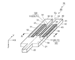
図1は、本発明の実施形態1に係る圧電振動子の構造を示す斜視図、図2は、図1のA
−A切断面を示す断面図及び各電極の接続説明図である。なお、本発明の圧電振動子の材
質としては、圧電性能を有するものであれば限定されずに適合できるが、以下の実施形態
では、圧電振動子として周波数温度特性に優れる水晶振動子を例示して説明する。図1、
図2において、水晶振動子10は、水晶振動片20の表面に複数の電極と、圧電体薄膜素
子100,101と、圧電体薄膜素子100,101それぞれの上面に設けられる温度補
償膜110,111と、を有して構成されている。
FIG. 1 is a perspective view showing the structure of a piezoelectric vibrator according to
It is sectional drawing which shows -A cut surface, and connection explanatory drawing of each electrode. The material of the piezoelectric vibrator of the present invention is not limited as long as it has piezoelectric performance, but in the following embodiments, a quartz vibrator having excellent frequency temperature characteristics is exemplified as the piezoelectric vibrator. I will explain. FIG.
In FIG. 2, the
水晶振動片20は、基部21の一辺から、Y軸方向に平行に延在された一対の振動腕3
0,40を有した音叉型振動子である。そして、基部21の振動腕30,40の延在方向
とは逆方向に支持部22が設けられている。振動腕30,40は、中心線C0に対して対
称形である。また、水晶振動片20は、結晶軸方向をX軸方向にして切り出されている。
The quartz
It is a tuning fork type vibrator having 0 and 40. A
振動腕30には、一方の主面(第1面)31(以降、表面31と表す)を2分して、振動腕30の中心線C1に対して結晶軸方向(振動腕の内側方向、または第1領域)に圧電体薄膜(圧電体層)71、外側方向(第2領域)に電極(第1電極)51が形成され、表面31に対向する主面(第2面)32(以降、裏面32と表す)に電極(第1電極)53が形成されている。なお、電極53は、圧電体薄膜71及び電極51にそれぞれ対向するように2分割する構成としてもよく、省略することもできる。
The
また、振動腕30の外側側面33には電極(第2電極)52が、内側側面34には電極(第2電極)54が形成されている。さらに、圧電体薄膜71の表面には電極(第3電極)55が形成され、電極55の上面には温度補償膜(温度補償層)110が設けられている。
Further, an electrode (second electrode) 52 is formed on the
振動腕40には、一方の主面(第1面)41(以降、表面41と表す)を2分して、振動腕40の中心線C2に対して結晶軸方向(振動腕の外側方向、または第2領域)に圧電体薄膜(圧電体層)72、内側方向(第1領域)に電極(第1電極)56が形成され、他方の主面(第2面)42(以降、裏面42と表す)に電極(第1電極)58が形成されている。なお、電極58は、圧電体薄膜72及び電極56に対向するように2分割する構成としてもよく、省略してもよい。
In the vibrating
また、振動腕40の外側側面43には電極(第2電極)59が、内側側面44には電極(第2電極)57が形成されている。さらに、圧電体薄膜72の表面には電極(第3電極)60が形成され、電極60の上面には温度補償膜(温度補償層)111が設けられている。
Further, an electrode (second electrode) 59 is formed on the
圧電体薄膜71,72の材質としては、ZnO、AlN、GaN、PZT(登録商標)
、KN、LN、LT等から選択することができ、本実施形態では、水晶よりも誘電率が大
きく、しかもその差が大きい材料、ヤング率が大きい材料、電気機械結合係数K2が大き
い材料を選択する。
As the material of the piezoelectric
, KN, LN, LT, and the like. In this embodiment, a material having a larger dielectric constant than quartz, a material having a large difference, a material having a large Young's modulus, and a material having a large electromechanical coupling coefficient K 2 are used. select.
また、温度補償膜110,111の材質としては、Ni−鉄合金、酸化シリコン、酸化
テリル、酸化ジルコニウム等を採用でき、圧電体薄膜71,72の一次温度係数に対して
逆の一次温度係数を有するものから選択する。具体的には、圧電体薄膜71,72が負の
一次温度係数を有するとき、温度補償膜110,111は正の一次温度係数を有する。
Further, as a material of the
電極55,51,53,57,59及び接続端子93は、接続電極91によって接続さ
れる。また、これらの電極とは互いに異極となる電極52,54,58,60,56及び
接続端子94は、接続電極92によって接続されている。そして、接続端子93,94に
それぞれ互いに逆相の交流電圧を印加することで、振動腕30,40がX軸方向に屈曲振
動する。従って、電極51〜60は、水晶振動片20の励振電極である。
The
図3は、水晶振動子を特定の振動モードで励振する発振回路に接続した状態を示す等価
回路図である。図3において、発振器80は、増幅回路81と帰還回路82とを含んでい
る。
FIG. 3 is an equivalent circuit diagram showing a state in which the crystal resonator is connected to an oscillation circuit that excites in a specific vibration mode. In FIG. 3, the
増幅回路81は、増幅器83と帰還抵抗84とを含んで構成されている。帰還回路82
は、ドレイン抵抗85とコンデンサ86,87と水晶振動子10を含んで構成されている
。水晶振動子10は、水晶振動片20と圧電体薄膜素子100,101とが直列に接続さ
れている(図2も参照する)。
The
Includes a
ここで、増幅器83はCMOSインバータを用いることができる。このような構成によ
り、水晶振動片20と圧電体薄膜素子100,101とが同一振動モードで振動する発振
器80を形成することができる。
Here, the
続いて、本実施形態に係る水晶振動子の駆動について図面を参照して説明する。
図4は、水晶振動子の駆動について模式的に示す説明図である。なお、図4は、図1の
A−A切断面を表している。
図4(a)を参照して第1の状態を説明する。電極51,53,55,57,59には
マイナス(−)電位を印加し、電極52,54,56,58,60にはプラス(+)電位
を印加する。ここで、振動腕30,40の水晶の結晶軸方向を矢印Dで表し、圧電体薄膜
71,72の分極方向を矢印P0で表している。
Next, driving of the crystal resonator according to the present embodiment will be described with reference to the drawings.
FIG. 4 is an explanatory diagram schematically showing driving of the crystal resonator. FIG. 4 shows the AA cut surface of FIG.
The first state will be described with reference to FIG. A negative (−) potential is applied to the
まず、振動腕30について説明すると、圧電体薄膜71は、電極55と電極54によっ
て挟まれた圧電体薄膜素子100が形成された状態であり(水晶を一部介在する)、電極
55にマイナス電位、電極54にプラス電位を印加すると厚さ(Z軸)方向に縮み、幅(
X軸)方向及び長さ(Y軸)方向に伸びる。
First, the vibrating
X-axis) direction and length (Y-axis) direction.
従って、圧電体薄膜71は、水晶の結晶軸方向の偏った位置に設けられているために、
振動腕30を矢印F1方向に変位しようとする。振動腕30は、電極それぞれに電圧を印
加すると矢印E方向に電界が発生し、やはり矢印F1方向に変位しようとするため、振動
腕30は圧電体薄膜素子100と共に、矢印F1方向に変位する。
Therefore, the piezoelectric
An attempt is made to displace the vibrating
次に、振動腕40について説明する。圧電体薄膜72は、電極60と電極59によって
挟まれた圧電体薄膜素子101が形成された状態であり(水晶を一部介在する)、電極6
0にプラス電位、電極59にマイナス電位を印加すると厚さ(Z軸)方向に伸び、幅(X
軸)方向及び長さ(Y軸)方向に縮む。
Next, the vibrating
When a positive potential is applied to 0 and a negative potential is applied to the
(Axis) direction and length (Y axis) direction.
従って、圧電体薄膜72は、水晶の結晶軸方向の偏った位置に設けられているために、
振動腕40を矢印F2方向に変位しようとする。振動腕40は、電極それぞれに電圧を印
加すると矢印E方向に電界が発生し、やはり矢印F2方向に変位しようとするため、振動
腕40は圧電体薄膜素子101と共に、矢印F2方向に変位する。
このようにして、振動腕30,40は共に、図4(b)に示すように外側方向に変位す
る。
Therefore, since the piezoelectric
Attempts to displace the vibrating
In this way, the vibrating
次に、第2の状態を説明する(図示は省略する)。第2の状態は、上述した第1の状態
に対して、各電極に逆相の電圧を印加した状態を示している。つまり、電極51,53,
55,57,59にはプラス(+)電位を印加し、電極52,54,56,58,60に
はマイナス(−)電位を印加する。
Next, the second state will be described (illustration is omitted). The 2nd state has shown the state which applied the voltage of the reverse phase to each electrode with respect to the 1st state mentioned above. That is, the
A positive (+) potential is applied to 55, 57 and 59, and a negative (−) potential is applied to the
まず、振動腕30について説明する。電極55にプラス電位、電極54にマイナス電位
を印加すると、圧電体薄膜71は厚さ(Z軸)方向に伸び、幅(X軸)方向及び長さ(Y
軸)方向に縮む。
First, the vibrating
Shrink in the (axis) direction.
従って、圧電体薄膜71は、振動腕30を矢印F3方向に変位しようとする。振動腕3
0は、電極それぞれに電圧を印加すると第1の状態(図4(a)、参照)とは逆方向に電
界が発生し、やはり矢印F3方向に変位しようとするため、振動腕30は圧電体薄膜素子
100と共に、矢印F3方向に変位する。
Accordingly, the piezoelectric
0, for the application of a voltage to each electrode and the first state (FIG. 4 (a), reference) electric field is generated in the opposite direction to the attempts also displaced in the arrow F 3 direction, the vibrating
次に、振動腕40について説明する。電極60にマイナス電位、電極59にプラス電位
を印加すると、圧電体薄膜72は厚さ(Z軸)方向に縮み、幅(X軸)方向及び長さ(Y
軸)方向に伸びる。従って、圧電体薄膜72は、矢印F4方向に変位しようとする。振動
腕40は、電極それぞれに電圧を印加すると第1の状態(図4(a)、参照)とは逆方向
に電界が発生し、やはり矢印F4方向に変位しようとするため、振動腕40は圧電体薄膜
素子101と共に、矢印F4方向に変位する。
Next, the vibrating
Axial) direction. Accordingly, the piezoelectric
上述した第1の状態と第2の状態を繰り返す(つまり、交流電圧を印加する)と振動腕
30,40は、X軸方向に屈曲振動を繰り返す。
When the first state and the second state described above are repeated (that is, an alternating voltage is applied), the vibrating
なお、上述した実施形態1では、圧電体薄膜素子100,101を振動腕30,40の
それぞれの表面31,41に形成する構造を例示したが、圧電体薄膜素子100,101
を、裏面32,42に形成する構造としてもよい。この際、電極51と電極53、電極5
6と電極58とを入れ替える構成とする。
In the first embodiment, the piezoelectric
May be formed on the back surfaces 32 and 42. At this time, the
6 and the
続いて、温度補償膜110,111について説明する。
図5は、温度補償膜110,111の温度と一次の周波数温度変化量との関係、つまり
、一次温度係数を模式的に表すグラフである。ここで、圧電体薄膜71,72の一次温度
係数df/fは負の傾き(具体的には−40ppm/deg)を有している。従って、温
度補償膜110,111の一次温度係数df/fを正の傾き(具体的には+40ppm/
deg)にすれば、圧電体薄膜の一次温度係数df/fを“0”にすることが可能となる
。
Next, the
FIG. 5 is a graph schematically showing the relationship between the temperature of the
deg), the primary temperature coefficient df / f of the piezoelectric thin film can be set to “0”.
次に、圧電体薄膜71,72の一次温度係数が水晶振動子に与える影響について説明す
る。
図6は、水晶振動子の温度変化に対する周波数変化量(周波数温度特性)を模式的に表
すグラフである。図6において、水晶振動子10の周波数温度特性(図中、実線で表す)
は、頂点温度T0とする二次曲線で表される。ここで、水晶振動子10に圧電体薄膜71
,72を付加下場合に、周波数温度特性は、頂点温度T0がマイナス方向に移動して頂点
温度T1を有する二次曲線(図中、破線で表す)で表される。従って、本来の水晶振動子
周波数温度特性(頂点温度T1の二次曲線)に補償する必要が生じ、温度補償膜110,
111を設ける。なお、温度補償膜の一次温度係数は、材質とその膜厚さによって変化す
る。
Next, the influence of the primary temperature coefficient of the piezoelectric
FIG. 6 is a graph schematically showing a frequency change amount (frequency temperature characteristic) with respect to a temperature change of the crystal resonator. In FIG. 6, the frequency-temperature characteristic of the crystal unit 10 (represented by a solid line in the figure).
Is represented by a quadratic curve with apex temperature T 0 . Here, the piezoelectric
, 72 is added, the frequency temperature characteristic is represented by a quadratic curve (represented by a broken line in the figure) in which the vertex temperature T 0 moves in the minus direction and has the vertex temperature T 1 . Therefore, it is necessary to compensate for the original crystal resonator frequency temperature characteristic (secondary curve of the vertex temperature T 1 ), and the
111 is provided. The primary temperature coefficient of the temperature compensation film varies depending on the material and the film thickness.
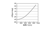
図7は、水晶振動片20に温度補償膜110,111を設けたときの温度補償膜の膜厚
さhと一次の周波数温度変化量df/fの関係を表すグラフである。ここでは、温度補償
膜110,111の材質を酸化シリコン(SiO2)とする。図7において、温度補償膜
110、111の膜厚さhが増加するに従い一次の周波数温度変化量df/fが増加する
。従って、一次の周波数温度変化量が“0”となる膜厚さh(具体的には550nm近傍
)とすれば、圧電体薄膜71,72の一次温度係数の影響を排除することができ、図6に
示す頂点温度T0の周波数温度特性を得ることができる。
FIG. 7 is a graph showing the relationship between the thickness h of the temperature compensation film and the primary frequency temperature change amount df / f when the
従って、上述した実施形態1によれば、水晶振動片20と圧電体薄膜素子100,10
1とを直列に接続し、水晶振動片20と圧電体薄膜素子100,101とを同一励振信号
で励振することにより、水晶振動片20と圧電体薄膜素子100,101とが相互に振動
を補完し合い、低周波領域において水晶振動子10の小型化を実現できる。
Therefore, according to the first embodiment described above, the quartz
1 are connected in series, and the
ここで、消費電力に影響を与える水晶振動子10のコンデンサ容量について考察する。
コンデンサ容量Cは、誘電体の面積S、厚さ(電極間距離)d、誘電率をεとすれば、C
=ε・S/dで表される。圧電体薄膜71,72の誘電率εz、水晶の誘電率εqの関係
は、それぞれの材料をεz≫εq、圧電体薄膜71,72の厚さdzと水晶振動片20の
厚さdqの関係を、dq≫dzとなるように設定している。従って、水晶振動片20のコ
ンデンサ容量Cqと圧電体薄膜71,72のコンデンサ容量Czの関係は、Cz≫Cqと
なる。
Here, the capacitor capacity of the
Capacitor capacity C is expressed as C if dielectric area S, thickness (distance between electrodes) d, and dielectric constant ε.
= Ε · S / d The relationship between the dielectric constant εz of the piezoelectric
本実施形態では、発振器80の等価回路において、水晶振動片20と圧電体薄膜素子1
00,101とを直列に接続している。従って、水晶振動子10の総コンデンサ容量Cは
、1/C=1/Cq+1/Czで表される。ここで、Cz≫Cqとしているため、C≒C
qと考えることができる。このことから、水晶振動子10の総コンデンサ容量Cを小さく
することができ、消費電力を増加させずに、水晶振動子の小型化を実現できる。
In the present embodiment, in the equivalent circuit of the
00 and 101 are connected in series. Therefore, the total capacitor capacity C of the
q can be considered. Thus, the total capacitor capacity C of the
また、圧電体薄膜素子100,101の電気機械結合係数K2は、水晶振動片20の電
気機械結合係数よりも大きい。性能指数MはM≒K2・Qで表すことができ、圧電体薄膜
素子100,101の電気機械結合係数(K2で表される)を水晶よりも大きくすること
で、圧電体薄膜素子100,101の性能指数Mが高くなる。従って、電気機械結合係数
が大きいほど振動しやすいので、薄い圧電体薄膜71,72により水晶振動片20の振動
を高効率化することができる。
Further, the electromechanical coupling coefficient K 2 of the piezoelectric
また、本実施形態では、圧電振動片として水晶振動子を採用し、圧電体薄膜71,72
の表面に、圧電体薄膜71,72とは逆の一次温度係数を有する温度補償膜110,11
1を設けることによって、圧電体薄膜71,72の一次温度係数を打ち消すので、圧電体
薄膜を用いる構造であっても、水晶振動子10が本来有する優れた周波数温度特性を活用
することができる。
(実施形態2)
In this embodiment, a crystal resonator is used as the piezoelectric vibrating piece, and the piezoelectric
1 is cancelled, the primary temperature coefficient of the piezoelectric
(Embodiment 2)
続いて、本発明の実施形態2について図面を参照して説明する。実施形態2は、前述し
た実施形態1に対して、温度補償膜を圧電体薄膜と電極との間(つまり、圧電体薄膜素子
の上面)に設けることを特徴としている。従って、相違部分を中心に説明し、実施形態1
と同じ符号を附して説明する。
図8は、実施形態2に係る水晶振動子の断面図(図1のA−A切断面に相当する)及び
各電極の接続説明図である。図8において、振動腕30の表面31には圧電体薄膜71、
圧電体薄膜71の表面に温度補償膜110、温度補償膜110の表面に電極55が設けら
れている。
Subsequently, Embodiment 2 of the present invention will be described with reference to the drawings. The second embodiment is characterized in that a temperature compensation film is provided between the piezoelectric thin film and the electrode (that is, the upper surface of the piezoelectric thin film element) as compared with the first embodiment described above. Therefore, the description will focus on the differences, and the first embodiment will be described.
The same reference numerals are used for explanation.
FIG. 8 is a cross-sectional view of the crystal resonator according to the second embodiment (corresponding to the AA cut surface of FIG. 1) and a connection explanatory diagram of each electrode. In FIG. 8, a piezoelectric
A
従って、圧電体薄膜71と温度補償膜110とは積層された状態で振動腕30の一部を
介在して電極55と電極54との間に挟まれた圧電体薄膜素子100を構成している。
Accordingly, the piezoelectric
また、振動腕40の表面41には圧電体薄膜72、圧電体薄膜72の表面に温度補償膜
111、温度補償膜111の上面に電極60が設けられている。
A piezoelectric
従って、圧電体薄膜72と温度補償膜111とは積層された状態で振動腕40の一部を
介在して電極60と電極59との間に挟まれた圧電体薄膜素子101を構成している。
Accordingly, the piezoelectric
なお、電極51〜60及び接続端子93,94の接続は、前述した実施形態1と同様に
行われており、接続端子93,94に交流電圧を印加することで、振動腕30,40が屈
曲振動する。
The
図9は、水晶振動子の駆動について模式的に示す説明図である。図9(a)を参照して
第1の状態を説明する。電極51,53,55,57,59にはマイナス(−)電位を印
加し、電極52,54,56,58,60にはプラス(+)電位を印加する。ここで、振
動腕30,40の水晶の結晶軸方向を矢印Dで表し、圧電体薄膜71,72の分極方向を
矢印P0で表している。
FIG. 9 is an explanatory diagram schematically showing driving of the crystal unit. The first state will be described with reference to FIG. A negative (−) potential is applied to the
まず、振動腕30について説明すると、電極55にマイナス電位、電極54にプラス電
位を印加すると厚さ(Z軸)方向に縮み、幅(X軸)方向及び長さ(Y軸)方向に伸びる
。
First, the vibrating
従って、圧電体薄膜素子100が、水晶の結晶軸方向の偏った位置に設けられているた
めに、振動腕30を矢印F1方向に変位しようとする。振動腕30は、電極それぞれに電
圧を印加すると矢印E方向に電界が発生し、やはり矢印F1方向に変位しようとするため
、振動腕30は圧電体薄膜素子100と共に、矢印F1方向に変位する。
Therefore, since the piezoelectric
次に、振動腕40について説明する。電極60にプラス電位、電極59にマイナス電位
を印加すると厚さ(Z軸)方向に伸び、幅(X軸)方向及び長さ(Y軸)方向に縮む。
Next, the vibrating
従って、圧電体薄膜素子101が、水晶の結晶軸方向の偏った位置に設けられているた
めに、振動腕40を矢印F2方向に変位しようとする。振動腕40は、電極それぞれに電
圧を印加すると矢印E方向に電界が発生し、やはり矢印F2方向に変位しようとするため
、振動腕40は圧電体薄膜素子101と共に、矢印F2方向に変位する。
このようにして、振動腕30,40は共に、図9(b)に示すように外側方向(矢印F
1,F2方向)に変位する。
Therefore, since the piezoelectric
In this way, the vibrating
1, displaced in the F 2 direction).
次に、第2の状態を説明する(図示は省略する)。第2の状態は、上述した第1の状態
に対して、各電極に逆相の電圧を印加した状態を示している。つまり、電極51,53,
55,57,59にはプラス(+)電位を印加し、電極52,54,56,58,60に
はマイナス(−)電位を印加する。
Next, the second state will be described (illustration is omitted). The 2nd state has shown the state which applied the voltage of the reverse phase to each electrode with respect to the 1st state mentioned above. That is, the
A positive (+) potential is applied to 55, 57 and 59, and a negative (−) potential is applied to the
まず、振動腕30について説明する。電極55にプラス電位、電極54にマイナス電位
を印加すると、圧電体薄膜71は厚さ(Z軸)方向に伸び、幅(X軸)方向及び長さ(Y
軸)方向に縮む。
First, the vibrating
Shrink in the (axis) direction.
従って、圧電体薄膜素子100は、振動腕30を図9に示す矢印F3方向に変位しよう
とする。振動腕30は、電極それぞれに電圧を印加すると図9の矢印Eとは逆方向に電界
が発生し、やはり矢印F3方向に変位しようとするため、振動腕30は圧電体薄膜素子1
00と共に、矢印F3方向に変位する。
Therefore, the piezoelectric
With 00, is displaced in the arrow F 3 direction.
次に、振動腕40について説明する。電極60にマイナス電位、電極59にプラス電位
を印加すると、圧電体薄膜72は厚さ(Z軸)方向に縮み、幅(X軸)方向及び長さ(Y
軸)方向に伸びる。
Next, the vibrating
Axial) direction.
従って、圧電体薄膜素子101は、矢印F4方向に変位しようとする。振動腕40は、
電極それぞれに電圧を印加すると図9の矢印Eとは逆方向に電界が発生し、やはり矢印F
4方向に変位しようとするため、振動腕40は圧電体薄膜素子101と共に、矢印F4方向
に変位する。
Therefore, the piezoelectric
When a voltage is applied to each electrode, an electric field is generated in the direction opposite to the arrow E in FIG.
In order to displace in four directions, the vibrating
接続端子93,94に交流電圧を印加し、上述した第1の状態と第2の状態を繰り返す
と振動腕30,40は、図9(b)に示すようにX軸方向に屈曲振動を繰り返す。
When an AC voltage is applied to the
次に、温度補償膜110,111それぞれが電極55,60と圧電体薄膜71,72の
間に設けられる実施形態2の構成による温度補償について説明する。このような構成にお
いても温度補償膜110,111の一次温度係数は、材質とその膜厚さによって変化する
。
Next, temperature compensation by the configuration of the second embodiment in which the
図10は、水晶振動片20に温度補償膜110,111を設けたときの温度補償膜の膜
厚さhと一次の周波数温度変化量df/fの関係を表すグラフである。ここでは、温度補
償膜110の材質を酸化シリコン(SiO2)とする。なお、実施形態1の構成との比較
を表している。図10において、温度補償膜110,111の膜厚さhが増加するに従い
一次の周波数温度変化量が増加する。
FIG. 10 is a graph showing the relationship between the thickness h of the temperature compensation film and the primary frequency temperature variation df / f when the
ここで、実施形態2の構成(上層から電極−温度補償膜−圧電体薄膜の構成)では、実
施形態1の構成(上層から温度補償膜−電極−圧電体薄膜の構成)よりも、膜厚さに対し
て一次の周波数温度変化量(df/f)が敏感に変化する。そして、一次の周波数温度変
化量が“0”となる膜厚さh(具体的には50nm近傍)とすれば、圧電体薄膜の一次温
度係数の影響を排除することができることを示している。
Here, in the configuration of the second embodiment (from the upper layer to the electrode-temperature compensation film-piezoelectric thin film), the film thickness is larger than that in the configuration of the first embodiment (from the upper layer to the temperature compensation film-electrode-piezoelectric thin film). The first-order frequency temperature variation (df / f) changes sensitively. Then, it is shown that the influence of the primary temperature coefficient of the piezoelectric thin film can be eliminated by setting the film thickness h (specifically around 50 nm) at which the primary frequency temperature change amount is “0”.
図10を参照して実施形態1と実施形態2の構成による特性の相違を比較する。実施形
態1によれば、膜厚さhに対して一次の周波数温度変化量df/fが鈍感であり、膜厚さ
hが変化しても一次の周波数温度変化量df/fが小さいので、量産安定性に優れるとい
う効果がある。
With reference to FIG. 10, the difference in characteristics according to the configurations of the first embodiment and the second embodiment is compared. According to the first embodiment, the primary frequency temperature change amount df / f is insensitive to the film thickness h, and even if the film thickness h changes, the primary frequency temperature change amount df / f is small. There is an effect of excellent mass production stability.
また、実施形態2によれば、膜厚さhに対して一次の周波数温度変化量df/fが敏感
であり、膜厚さhも50nmと薄くてよい。従って、成膜時間が短縮できる他、成膜によ
る膜応力も小さくて済むため、圧電振動片の反り等の変形が発生しにくいという効果もあ
る。
Further, according to the second embodiment, the primary frequency temperature change amount df / f is sensitive to the film thickness h, and the film thickness h may be as thin as 50 nm. Therefore, the film formation time can be shortened, and the film stress due to film formation can be reduced, so that there is an effect that deformation such as warpage of the piezoelectric vibrating reed hardly occurs.
また、実施形態1及び実施形態2による構造では共に温度補償膜110,111の膜厚
さhを増減することで、図10に示すように、一次の周波数温度変化量df/f(つまり
、一次温度係数)を調整することができる。ここで、温度補償膜110,111の膜厚さ
hの調整方法を含む水晶振動子の製造方法について説明する。図示は省略する。
Further, in the structures according to the first and second embodiments, by increasing or decreasing the film thickness h of the
まず、大判の圧電基板としての水晶基板(水晶ウエハと呼称することがある)に、フォ
トリソグラフィ技術によって複数の水晶振動片20を形成する。この際、水晶振動片の基
部21または支持部22(図1、参照)を水晶基板に接続しておく。
First, a plurality of
続いて、圧電体薄膜71,72を形成する。実施形態1の構造では、振動腕30,40
のそれぞれの表面31,41の所定位置に第1圧電体薄膜を形成する。第1圧電体薄膜の
形成方法は、RFスパッタリング法等のPVD(Physical Vapor Dep
osition)法であてもよいし、CVD(Chemical Vapor Depo
sition)法であってもよい。また、第1圧電体薄膜の厚さは、5nm〜100nm
が好ましい。
Subsequently, piezoelectric
A first piezoelectric thin film is formed at a predetermined position on each of the
oxidization) method, or CVD (Chemical Vapor Depo)
(situation) method. The thickness of the first piezoelectric thin film is 5 nm to 100 nm.
Is preferred.
続いて、第1圧電体薄膜の熱処理を行い、熱処理後の第1圧電体薄膜を形成する。熱処
理は、ランプ加熱、レーザー光加熱であってもよいが、400℃以下での熱処理は、温度
管理ができ温度を低温から上昇できる熱処理方法が好ましい。具体的には、より安定した
温度管理ができる熱処理炉、ホットプレート、真空チャンバ中での熱処理が好ましい。こ
の熱処理後の第1圧電体薄膜は結晶化が進んだ状態である。
Subsequently, the first piezoelectric thin film is heat treated to form a heat treated first piezoelectric thin film. The heat treatment may be lamp heating or laser light heating, but the heat treatment at 400 ° C. or lower is preferably a heat treatment method in which the temperature can be controlled and the temperature can be raised from a low temperature. Specifically, heat treatment in a heat treatment furnace, hot plate, or vacuum chamber capable of more stable temperature management is preferable. The first piezoelectric thin film after the heat treatment is in a state where crystallization has progressed.
続いて、熱処理後の第1圧電体薄膜上に第2圧電体薄膜を形成する。第2圧電体薄膜は
、結晶化が進んだ熱処理後の第1圧電体薄膜上において結晶生長する材料であればどのよ
うな圧電体薄膜でもよいが、本実施形態では、第1圧電体薄膜と同じ材料を採用している
。
Subsequently, a second piezoelectric thin film is formed on the first piezoelectric thin film after the heat treatment. The second piezoelectric thin film may be any piezoelectric thin film as long as it is a material that grows crystals on the first piezoelectric thin film after the heat treatment that has been crystallized. In the present embodiment, The same material is used.
第2圧電体薄膜も、PVD法、CVD法等の成膜法で形成することが可能で、その厚さ
は数μmである。この第2圧電体薄膜は、熱処理後の第1圧電体薄膜を含めて圧電体薄膜
71,72となる。
The second piezoelectric thin film can also be formed by a film forming method such as a PVD method or a CVD method, and the thickness thereof is several μm. The second piezoelectric thin film becomes the piezoelectric
このようにして圧電体薄膜71,72を形成した後、電極51〜60を形成する。圧電
体薄膜71,72それぞれの上面に形成する電極55,60は他の電極と同時形成しても
よいし、別工程で形成してもよい。
After the piezoelectric
電極51〜60を形成した後、温度補償膜110,111を形成する。温度補償膜11
0,111はチャンバ内でPVD法またはCVD法等の成膜法で形成する。この成膜工程
の際、チャンバ内に周波数計測モニタを備え、一次温度係数をモニタしながら、一次の周
波数温度変化量が“0”になる膜厚さhを調整する。
After forming the
0 and 111 are formed in the chamber by a film forming method such as a PVD method or a CVD method. During this film formation process, a frequency measurement monitor is provided in the chamber, and the film thickness h at which the primary frequency temperature change amount is “0” is adjusted while monitoring the primary temperature coefficient.
または、予め膜厚さを厚い方向に形成しておき、温度補償膜の表面をエッチング等によ
り研削して一次の周波数温度変化量df/fが“0”になる膜厚さhを得る方法としても
よい。
Alternatively, as a method of obtaining a film thickness h in which the primary frequency temperature change amount df / f is “0” by forming the film thickness in a thick direction in advance and grinding the surface of the temperature compensation film by etching or the like. Also good.
そして、温度補償膜110,111を形成した後、水晶基板11をダイシング等で切断
して、水晶振動子10を切り離し個片化する。
Then, after the
また、実施形態2の構造では、圧電体薄膜71,72を形成後、温度補償膜110,1
11を形成し、温度補償膜110,111の上面に電極55,60を形成する。圧電体薄
膜71,72及び温度補償膜110,111の形成方法は、上述した実施形態1の方法と
同じである。また、温度補償膜110,111の成膜工程において、一次温度係数をモニ
タする。
In the structure of the second embodiment, the
11 and
なお、圧電体薄膜の結晶性を高める方法として、圧電体薄膜を金属薄膜の表面に形成す
る方法が採用できる。この方法は、振動腕30,40のそれぞれの表面31,41の所定
位置にPtまたはTiの金属薄膜を形成し、金属薄膜の表面に圧電体薄膜71,72を形
成する。圧電体薄膜71,72は、金属薄膜が存在するために良好な結晶性を有する。
As a method for improving the crystallinity of the piezoelectric thin film, a method of forming the piezoelectric thin film on the surface of the metal thin film can be employed. In this method, a Pt or Ti metal thin film is formed at predetermined positions on the
圧電体薄膜の振動特性は、圧電体薄膜の結晶性が良好なほどよい。従って、水晶基板の
表面に第1圧電体薄膜を形成し、この第1圧電体薄膜を熱処理した後、熱処理された前記
第1圧電体薄膜の表面に、第1圧電体薄膜と同一材料の第2圧電体薄膜を形成して結晶性
を改善している。その結果、優れた振動性能を得ることができる。
The vibration characteristics of the piezoelectric thin film are better as the crystallinity of the piezoelectric thin film is better. Therefore, after forming the first piezoelectric thin film on the surface of the quartz substrate, heat-treating the first piezoelectric thin film, the first piezoelectric thin film is made of the same material as the first piezoelectric thin film on the surface of the heat-treated first piezoelectric thin film. (2) A piezoelectric thin film is formed to improve crystallinity. As a result, excellent vibration performance can be obtained.
また、水晶基板の表面にPtまたはTiの少なくとも一方の金属薄膜を形成し、この金
属薄膜の表面に圧電体薄膜71,72を形成することで、圧電体薄膜71,72の結晶性
を高めることができる他、圧電体薄膜71,72と水晶振動片20との密着性を高めるこ
とができるという効果がある。
Further, by forming at least one metal thin film of Pt or Ti on the surface of the quartz substrate and forming the piezoelectric
また、温度補償膜110,111の成膜工程の際、チャンバ内に周波数計測モニタを備
え、チャンバ内にて一次温度係数をモニタしながら、一次の周波数温度変化量が“0”に
なる膜厚さhを得る方法により、生産性が高い水晶振動子を実現できる。
(実施形態3)
Further, during the film forming process of the
(Embodiment 3)
続いて、本発明の実施形態3に係る水晶振動子について図面を参照して説明する。実施
形態3は、振動腕30,40の表裏両面それぞれに圧電体薄膜素子を形成しているところ
に特徴を有している。従って、実施形態1との相違部分を中心に説明し、同じ部位には同
じ符号を附している。
図11は、実施形態3に係る水晶振動子の構成と駆動について模式的に示す断面図であ
る。なお、図11では、前述した実施形態1にて説明した圧電体薄膜−電極−温度補償膜
の構成を例示している。
図11において、振動腕30の裏面32には、圧電体薄膜素子100に対向して圧電体薄
膜素子102が形成されている。
Subsequently, a crystal resonator according to a third embodiment of the present invention will be described with reference to the drawings. The third embodiment is characterized in that piezoelectric thin film elements are formed on both front and back surfaces of the vibrating
FIG. 11 is a cross-sectional view schematically showing the configuration and driving of the crystal resonator according to the third embodiment. 11 illustrates the configuration of the piezoelectric thin film-electrode-temperature compensation film described in the first embodiment.
In FIG. 11, a piezoelectric
圧電体薄膜素子102の構成は、圧電体薄膜素子101と同じであり、振動腕30の裏
面32から圧電体薄膜73、電極61、温度補償膜112の順に積層形成されている。
従って、圧電体薄膜73は、電極61,54によって挟まれた圧電体薄膜素子102を構
成する。
The configuration of the piezoelectric
Therefore, the piezoelectric
一方、振動腕40の裏面42には、圧電体薄膜素子101に対向して圧電体薄膜素子1
03形成され、電極56に対向して電極58が形成されている。従って、圧電体薄膜74
は、電極62,59によって挟まれた圧電体薄膜素子103を構成する。
なお、圧電体薄膜71〜74は実施形態1と同様な材料としての条件を満たし、厚さ、
平面形状も同じとする。
On the other hand, on the
03, and an
Constitutes the piezoelectric
The piezoelectric
The planar shape is the same.
次に、水晶振動片20の駆動について説明する。電極51,53,55,57,59,
61にはマイナス(−)電位を印加し、電極52,54,58,62,60,56にはプ
ラス(+)電位を印加する。
Next, driving of the
A negative (−) potential is applied to 61, and a positive (+) potential is applied to the
まず、振動腕30について説明する。圧電体薄膜71,73は、電極55,61にマイ
ナス電位、電極54にプラス電位を印加すると厚さ(Z軸)方向に縮み、幅(X軸)方向
及び長さ(Y軸)方向に伸びる。
First, the vibrating
従って、圧電体薄膜71,73は、振動腕30の水晶の結晶軸方向に偏った位置に設け
られていることから、それぞれ同じように振動腕30を矢印F1方向に変位しようとする
。振動腕30は、電極それぞれに電圧を印加すると矢印E方向に電界が発生し、やはり矢
印F1方向に変位しようとするため、振動腕30は圧電体薄膜素子100,102と共に
、矢印F1方向に変位する。
Therefore, the piezoelectric
次に、振動腕40について説明する。圧電体薄膜72は、電極60にプラス電位、電極
59にマイナス電位を印加すると厚さ(Z軸)方向に伸び、幅(X軸)方向及び長さ(Y
軸方向)に縮む。
Next, the vibrating
Shrink in the axial direction.
また、圧電体薄膜74は、電極59にマイナス電位、電極62にプラス電位を印加する
と厚さ(Z軸)方向に伸び、幅(X軸)方向及び長さ(Y軸方向)に縮む。
Further, when a negative potential is applied to the
従って、圧電体薄膜72,74は、振動腕40の水晶の結晶軸方向に偏った位置に設け
られていることから、それぞれ同じように振動腕40を矢印F2方向に変位しようとする
。振動腕40は、電極それぞれに電圧を印加すると矢印E方向に電界が発生し、やはり矢
印F2方向に変位しようとするため、振動腕40は圧電体薄膜素子101,103と共に
、矢印F2方向に変位する。
このようにして、振動腕30,40は、図9(b)に示すように外側方向(矢印F1,
F2方向)に変位する。
Accordingly, since the piezoelectric
In this way, the vibrating
Displaced in the F 2 direction).
次に、図11で示した状態に対して各電極に逆相の電位を印加した場合について説明す
る。図示は省略するが。電極52,54,58,62,60,56にはマイナス電位、電
極51,53,61,55,57,59にはプラス電位の電圧を印加する。こうすること
で、圧電体薄膜71〜74の伸縮方向が図11(a)にあらわす状態とは逆方向となり、
振動腕30,40は図11(a)にて表す矢印F3,F4方向に変位する。
従って、接続端子93,94に交流電圧を印加することで、振動腕30,40は図11
(b)に表すようにX軸方向に屈曲振動を継続する。
Next, a case where a reverse phase potential is applied to each electrode in the state shown in FIG. 11 will be described. Illustration is omitted. A negative potential is applied to the
The vibrating
Accordingly, by applying an AC voltage to the
As shown in (b), the bending vibration is continued in the X-axis direction.
従って、上述したように、振動腕30,40それぞれの表裏両面に圧電体薄膜71,7
3、及び圧電体薄膜72,74を設けることにより、水晶振動片20と圧電体薄膜素子1
00〜103とが、より一層強く相互に振動を補完し合うことができる。また、一方の主
面(表裏面のどちらか一方)に圧電体薄膜を形成する場合よりも振動バランスをとること
ができ、捩れ等の不用振動を低減することができる。
Therefore, as described above, the piezoelectric
3 and the piezoelectric
00 to 103 can complement each other more strongly with each other. In addition, the vibration balance can be achieved as compared with the case where the piezoelectric thin film is formed on one main surface (either one of the front and back surfaces), and unnecessary vibration such as torsion can be reduced.
また、実施形態3の構造においても、温度補償膜110〜113を設けているので、圧
電体薄膜71〜74を設けることによる一次の周波数温度変化量df/fの影響を排除す
ることができる。
(実施形態4)
Also in the structure of the third embodiment, since the
(Embodiment 4)
次に、本発明の実施形態4について図面を参照して説明する。実施形態4は、前述した
実施形態3に対して、振動腕の側面にも圧電体薄膜素子を設けていることに特徴を有して
いる。従って、実施形態3との相違部分を中心に説明し、共通部位には実施形態3と同じ
符号を附している。
図12は、実施形態4に係る水晶振動子の構成と駆動について模式的に示す断面図である
。なお、図12では、前述した実施形態1にて説明した圧電体薄膜−電極−温度補償膜の
構成を例示している。
図12において、振動腕30の外側側面33には、圧電体薄膜素子104が形成されてい
る。
Next, a fourth embodiment of the present invention will be described with reference to the drawings. The fourth embodiment is characterized in that a piezoelectric thin film element is also provided on the side surface of the vibrating arm as compared with the third embodiment. Therefore, it demonstrates centering on a different part from Embodiment 3, and the same code | symbol as Embodiment 3 is attached | subjected to the common part.
FIG. 12 is a cross-sectional view schematically illustrating the configuration and driving of the crystal resonator according to the fourth embodiment. FIG. 12 illustrates the configuration of the piezoelectric thin film-electrode-temperature compensation film described in the first embodiment.
In FIG. 12, a piezoelectric
圧電体薄膜素子104の構成は、圧電体薄膜素子100〜103と同じであり、振動腕
30の外側側面33から圧電体薄膜75、電極63、温度補償膜114の順に積層形成さ
れている。
従って、圧電体薄膜75は、電極63と電極51,53によって挟まれた圧電体薄膜素子
104を構成する。
The configuration of the piezoelectric
Therefore, the piezoelectric
一方、振動腕40の内側側面44には、圧電体薄膜素子105が形成されている。圧電
体薄膜素子105の構成は、圧電体薄膜素子104と同じであり、振動腕40の内側側面
44から圧電体薄膜76、電極64、温度補償膜115の順に積層形成されている。従っ
て、圧電体薄膜76は、電極64と電極56,58によって挟まれた圧電体薄膜素子10
5を構成する。
なお、圧電体薄膜71〜76は実施形態1と同様な材料としての条件を満たし、厚さ、
平面形状も同じとする。
On the other hand, a piezoelectric
5 is configured.
The piezoelectric
The planar shape is the same.
次に、水晶振動片20の駆動について説明する。電極51,53,55,61,59,
64にはマイナス(−)電位を印加し、電極54,63,58,62,60,56にはプ
ラス(+)電位を印加する。
Next, driving of the
A negative (−) potential is applied to 64, and a positive (+) potential is applied to the
まず、振動腕30について説明すると、圧電体薄膜71,73の伸縮は、前述した実施
形態3と同じであり、厚さ(Z軸)方向に縮み、幅(X軸)方向及び長さ(Y軸)方向に
伸びる。
First, the vibrating
また、圧電体薄膜75は、電極51,53にマイナス電位、電極63にプラス電位を印
加すると厚さ(Z軸)方向に縮み、幅(X軸)方向及び長さ(Y軸)方向に伸びる。
The piezoelectric
従って、圧電体薄膜71,73,75は、振動腕30を矢印F1方向に変位しようとす
る。振動腕30は、電極それぞれに電圧を印加すると矢印E方向に電界が発生し、やはり
矢印F1方向に変位しようとするため、振動腕30は圧電体薄膜素子100,102,1
04と共に、矢印F1方向に変位する。
Therefore, the piezoelectric
With 04 displaced in direction of arrow F 1.
次に、振動腕40について説明する。圧電体薄膜72,74の伸縮は、前述した実施形
態3と同じであり、厚さ(Z軸)方向に伸び、幅(X軸)方向及び長さ(Y軸方向)に縮
む。
Next, the vibrating
また、圧電体薄膜76は、電極64にマイナス電位、電極56,58にプラス電位を印
加すると厚さ(Z軸)方向に伸び、幅(X軸)方向及び長さ(Y軸方向)に縮む。
The piezoelectric
従って、圧電体薄膜72,74,76は、振動腕40を矢印F2方向に変位しようとす
る。振動腕40は、電極それぞれに電圧を印加すると矢印E方向に電界が発生し、やはり
矢印F2方向に変位しようとするため、振動腕40は圧電体薄膜素子101,103,1
05と共に、矢印F2方向に変位する。
このようにして、振動腕30,40は、図12(b)に示すように外側方向に変位する
。
Therefore, the piezoelectric
With 05, is displaced in the arrow F 2 direction.
In this way, the vibrating
次に、図12(a)で示した状態に対して各電極に逆相の電位を印加する。図示は省略
するが、電極51,53,61,55,59,64にはプラス電位、電極54,63,5
6,58,62,60にはマイナス電位の電圧を印加する。こうすることで、圧電体薄膜
71〜76の伸縮方向が図12(a)に表す方向とは逆方向となり、振動腕30,40は
矢印F3,F4方向に変位する。
従って、接続端子93,94に交流電圧を印加することで、振動腕30,40は図12
(b)に示すようにX軸方向に屈曲振動を継続する。
Next, a reverse-phase potential is applied to each electrode with respect to the state shown in FIG. Although not shown, the
A negative potential voltage is applied to 6,58,62,60. By doing so, the expansion and contraction direction of the piezoelectric
Therefore, by applying an AC voltage to the
As shown in (b), the bending vibration is continued in the X-axis direction.
従って、上述した実施形態4によれば、水晶の厚さ方向(Z軸方向、振動腕の側面)に
も圧電体薄膜75,76を設けることにより、さらに強く相互に振動を補完し合うことが
でき、水晶振動子の振動効率を高めることができる。
Therefore, according to the fourth embodiment described above, by providing the piezoelectric
また、実施形態4の構造においても、温度補償膜110〜115を設けているので、圧
電体薄膜71〜76を設けることによる一次の周波数温度変化量の影響を排除することが
できる。
(実施形態5)
Also in the structure of the fourth embodiment, since the
(Embodiment 5)
続いて、本発明の実施形態5について図面を参照して説明する。前述した実施形態1,
2では圧電体薄膜素子100,101、実施形態3では圧電体薄膜素子100〜103、
実施形態4では圧電体薄膜素子100〜105をそれぞれ備えている。
Next, Embodiment 5 of the present invention will be described with reference to the drawings.
2, piezoelectric
In the fourth embodiment, the piezoelectric
しかしながら、圧電体薄膜素子を設けることにより、水晶振動片20の中心線C0に対
して振動腕30と振動腕40との質量バランス、あるいは、振動腕30,40それぞれの
中心線C1,C2に対する質量バランスがくずれることがある。そのことによって僅かであ
るが振動バランスがくずれることが考えられる。実施形態5では、そのような課題を解決
するためにバランス質量を付加することを特徴としている。なお、実施形態1〜実施形態
4と同じ部位には同じ符号を附している。また、バランス質量としては、圧電体薄膜と同
材質のものを採用する。
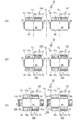
However, by providing the piezoelectric thin film element, the mass balance between the vibrating
図13(a)〜(c)は、実施形態5に係る水晶振動子を示す断面図である。なお、図
13(a)〜(c)に図示する構造は、実施形態1にて説明した温度補償膜の構成を例示
している。
図13(a)は、実施形態1(図2、参照)にて説明した構造に対してバランス質量を
付加した例を示している。図13(a)において、振動腕30には、中心線C1に対して
圧電体薄膜素子100と対称となるバランス質量77aが設けられている。つまり、バラ
ンス質量77aは、温度補償膜110と電極55と圧電体薄膜71の質量総和が、バラン
ス質量77aと電極51の質量総和と等しい。従って、振動腕30内において質量バラン
スがとれる。
13A to 13C are cross-sectional views illustrating the crystal resonator according to the fifth embodiment. Note that the structures illustrated in FIGS. 13A to 13C illustrate the configuration of the temperature compensation film described in the first embodiment.
FIG. 13A shows an example in which a balance mass is added to the structure described in the first embodiment (see FIG. 2). In FIG. 13 (a), the vibrating
振動腕40においても同様に、バランス質量77bを設けることにより、付加されたバ
ランス質量77bと電極56との積層体の質量総和は、圧電体薄膜72と電極60と温度
補償膜111の積層体の質量総和と等しく中心線C2に対して対称となり、振動腕40内
において質量バランスがとれている。
Similarly, in the vibrating
このように、バランス質量77a,77bを設けることにより、振動腕30,40が、
中心線C0に対しても質量バランスがとれ、振動バランスをとることができる。
Thus, by providing the
The mass balance is also achieved with respect to the center line C 0 , and the vibration balance can be achieved.
図13(b)は、実施形態3(図11、参照)に対してバランス質量を付加した例を示
している。実施形態3は、振動腕30,40の表裏両面それぞれに、圧電体薄膜素子10
0,102、圧電体薄膜素子101,103が設けられている構造である。振動腕30に
は中心線C1に対して圧電体薄膜素子100,102に対称なバランス質量77a,78
aを設け、振動腕40には中心線C2に対して圧電体薄膜素子101,103に対称とな
るバランス質量77b,78bを設けている。
FIG.13 (b) has shown the example which added balance mass with respect to Embodiment 3 (refer FIG. 11). In the third embodiment, the piezoelectric
0, 102, and piezoelectric
provided a, the vibrating
このようにバランス質量77a,77b及びバランス質量78a,78bを設けること
により、振動腕30及び振動腕40内において質量バランスがとれると共に、振動腕30
と振動腕40との質量バランスがとれ、そのことにより振動バランスがとれる。
Thus, by providing the
And the vibrating
図13(c)は、実施形態4(図12、参照)に対してバランス質量を付加した例を示
している。実施形態4は、振動腕30の表裏両面と側面それぞれに圧電体薄膜素子100
,102,104が設けられている構造であるので、振動腕30には中心線C1に対して
圧電体薄膜素子100,102,104それぞれに対称なバランス質量77a,78a,
79aを設ける。
FIG.13 (c) has shown the example which added balance mass with respect to Embodiment 4 (refer FIG. 12). In the fourth embodiment, the piezoelectric
Since in
79a is provided.
また、振動腕40の表裏両面と側面それぞれには、圧電体薄膜素子101,103,1
05が設けられている構造であるので、中心線C2に対して圧電体薄膜素子101,10
3,105それぞれに対称なバランス質量77b,78b,79bを設けている。
Further, the piezoelectric
Since a structure in which 05 is provided, the piezoelectric thin-film element with respect to the
3 and 105 are provided with
このようにバランス質量77a,77b及びバランス質量78a,78b及びバランス
質量79a,79bを設けることにより、振動腕30及び振動腕40内において質量バラ
ンスがとれると共に、振動腕30と振動腕40との質量バランスがとれ、そのことにより
振動バランスがとれる。
Thus, by providing the
なお、前述した実施形態2は、温度補償膜110,111それぞれが電極55,60と
圧電体薄膜71,72との間に設けられる構造であり、図13(a)、図13(b)、図
13(c)で表すバランス質量77a,77b及びバランス質量78a,78b及びバラ
ンス質量79a,79bを付加することで、質量バランスをとることができる。
The above-described second embodiment has a structure in which the
従って、上述した実施形態5によれば、圧電体薄膜素子100〜105に対応したバラ
ンス質量を付加することにより、振動腕30,40のに振動バランスをとり、高精度な振
動特性を得ることができる。
また、バランス質量を圧電体薄膜と同材質で形成すれば、圧電体薄膜と同じ装置でバラ
ンス質量を構成することができるので、高精度のバランス質量を付加することができる。
Therefore, according to the fifth embodiment described above, by adding a balance mass corresponding to the piezoelectric
Further, if the balance mass is formed of the same material as the piezoelectric thin film, the balance mass can be configured with the same device as the piezoelectric thin film, so that a highly accurate balance mass can be added.
なお、本発明は前述の実施の形態に限定されるものではなく、本発明の目的を達成でき
る範囲での変形、改良等は本発明に含まれるものである。
例えば、前述した実施形態1では、圧電体薄膜71,72を振動腕30,40のそれぞ
れの表面31,41に形成する構造、及び圧電体薄膜71,72を裏面32,42に形成
する構造を説明したが、振動腕30の表面31に圧電体薄膜71を形成し、振動腕40の
裏面42に圧電体薄膜72を形成してもよく、その逆にしてもよい。
It should be noted that the present invention is not limited to the above-described embodiment, but includes modifications and improvements as long as the object of the present invention can be achieved.
For example, in the first embodiment described above, the piezoelectric
また、前述した実施形態5では、付加するバランス質量を圧電体薄膜と同材質を用いて
いるが、バランス質量は、中心線C0,C1,C2に対して質量バランス(つまり振動バラ
ンス)がとれれば、同材質でなくてもよく、圧電体でなくてもよい。
In the fifth embodiment described above, the balance mass to be added is the same material as that of the piezoelectric thin film, but the balance mass is a mass balance (ie, vibration balance) with respect to the center lines C 0 , C 1 , C 2 . If it can be removed, the material may not be the same, and the material may not be a piezoelectric body.
従って、前述した実施形態1〜実施形態5によれば、水晶振動片に圧電体薄膜素子を設
けることにより水晶振動子の小型化と低消費電力化を実現し、さらに温度補償膜を設ける
ことにより、周波数温度変化量が小さい高精度の水晶振動子を提供できる。
Therefore, according to the first to fifth embodiments described above, by providing a piezoelectric thin film element on the crystal vibrating piece, it is possible to reduce the size and power consumption of the crystal resonator, and further by providing a temperature compensation film. In addition, it is possible to provide a high-accuracy crystal resonator with a small amount of frequency temperature change.
10…水晶振動子、20…水晶振動片、21…基部、30,40…振動腕、31,41
…水晶振動片の表面、32,42…水晶振動片の裏面、51〜60…電極、71,72…
圧電体薄膜、110,111…温度補償膜。
DESCRIPTION OF
... the surface of the quartz crystal vibrating piece, 32, 42 ... the back surface of the quartz crystal vibrating piece, 51-60 ... the electrodes, 71, 72 ...
Piezoelectric thin film, 110, 111... Temperature compensation film.
Claims (4)
前記基部から伸長する振動腕と、を有し、
前記振動腕は、第1面と、該第1面に対向する第2面と、前記第1面の端部と前記第2面の端部とを連結する側面と、を有し、
前記第1面および前記第2面には、前記振動腕の前記伸長する方向に第1電極が形成され、
前記側面には、前記振動腕の前記伸長する方向に第2電極が形成され、
前記第1面および前記第2面の少なくとも一方の面上には、圧電体層と温度補償層と第3電極とを含む積層部が形成され、
前記積層部は前記第1電極と並列に配置され、
前記第1電極と前記第2電極とは極性が異なり、前記第1電極と前記第3電極とは極性が同じであり、
前記温度補償層の1次温度係数の符号と、前記圧電体層の1次温度係数の符号とが逆に設定されていることを特徴とする圧電振動子。 The base,
A vibrating arm extending from the base,
The resonating arm has a first surface, a second surface facing the first surface, and a side surface connecting the end portion of the first surface and the end portion of the second surface,
A first electrode is formed on the first surface and the second surface in the extending direction of the vibrating arm,
A second electrode is formed on the side surface in the extending direction of the vibrating arm,
A laminated portion including a piezoelectric layer, a temperature compensation layer, and a third electrode is formed on at least one of the first surface and the second surface,
The stacked portion is arranged in parallel with the first electrode,
The first electrode and the second electrode have different polarities, and the first electrode and the third electrode have the same polarity,
The piezoelectric vibrator, wherein the sign of the primary temperature coefficient of the temperature compensation layer and the sign of the primary temperature coefficient of the piezoelectric layer are set in reverse .
前記温度補償層は、Ni−Fe合金、酸化シリコン、酸化テリル、および酸化ジルコニウムのいずれかの部材から形成されることを特徴とする圧電振動子。 The temperature compensation layer is formed of a member of any one of Ni-Fe alloy, silicon oxide, teryl oxide, and zirconium oxide.
前記振動腕は、第1振動腕および第2振動腕を備え、 The vibrating arm includes a first vibrating arm and a second vibrating arm,
前記第1振動腕および前記第2振動腕は、前記基部から並列に伸長し、且つ電極配置が互いに同じであり、 The first vibrating arm and the second vibrating arm extend in parallel from the base and have the same electrode arrangement.
前記第1振動腕の前記第1電極と、前記第1振動腕の前記第3電極と、前記第2振動腕の前記第2電極と、を互いに接続し、 Connecting the first electrode of the first vibrating arm, the third electrode of the first vibrating arm, and the second electrode of the second vibrating arm;
前記第1振動腕の前記第2電極と、前記第2振動腕の前記第1電極と、前記第2振動腕の前記第3電極と、を互いに接続することを特徴とする圧電振動子。 The piezoelectric vibrator, wherein the second electrode of the first vibrating arm, the first electrode of the second vibrating arm, and the third electrode of the second vibrating arm are connected to each other.
Priority Applications (1)
| Application Number | Priority Date | Filing Date | Title |
|---|---|---|---|
| JP2007034391A JP5034540B2 (en) | 2007-02-15 | 2007-02-15 | Piezoelectric vibrator, oscillator |
Applications Claiming Priority (1)
| Application Number | Priority Date | Filing Date | Title |
|---|---|---|---|
| JP2007034391A JP5034540B2 (en) | 2007-02-15 | 2007-02-15 | Piezoelectric vibrator, oscillator |
Publications (3)
| Publication Number | Publication Date |
|---|---|
| JP2008199438A JP2008199438A (en) | 2008-08-28 |
| JP2008199438A5 JP2008199438A5 (en) | 2010-03-18 |
| JP5034540B2 true JP5034540B2 (en) | 2012-09-26 |
Family
ID=39757973
Family Applications (1)
| Application Number | Title | Priority Date | Filing Date |
|---|---|---|---|
| JP2007034391A Expired - Fee Related JP5034540B2 (en) | 2007-02-15 | 2007-02-15 | Piezoelectric vibrator, oscillator |
Country Status (1)
| Country | Link |
|---|---|
| JP (1) | JP5034540B2 (en) |
Families Citing this family (2)
| Publication number | Priority date | Publication date | Assignee | Title |
|---|---|---|---|---|
| JP2008245243A (en) * | 2007-02-26 | 2008-10-09 | Epson Toyocom Corp | Contour resonator and adjustment method therefor |
| JP7005988B2 (en) * | 2017-04-27 | 2022-01-24 | セイコーエプソン株式会社 | MEMS devices, electronic devices and mobiles |
Family Cites Families (5)
| Publication number | Priority date | Publication date | Assignee | Title |
|---|---|---|---|---|
| JPS5549020A (en) * | 1978-10-04 | 1980-04-08 | Seiko Instr & Electronics Ltd | Piezoelectric vibrator |
| JPS5699929U (en) * | 1979-12-28 | 1981-08-06 | ||
| JP4434537B2 (en) * | 2001-08-27 | 2010-03-17 | パナソニック株式会社 | Piezoelectric functional parts |
| JP3972790B2 (en) * | 2001-11-27 | 2007-09-05 | 松下電器産業株式会社 | Thin film micromechanical resonator and thin film micromechanical resonator gyro |
| JP2005249646A (en) * | 2004-03-05 | 2005-09-15 | Matsushita Electric Ind Co Ltd | Tuning fork type oscillator for angular velocity sensor, angular velocity sensor using the oscillator, and automobile using the angular velocity sensor |
-
2007
- 2007-02-15 JP JP2007034391A patent/JP5034540B2/en not_active Expired - Fee Related
Also Published As
| Publication number | Publication date |
|---|---|
| JP2008199438A (en) | 2008-08-28 |
Similar Documents
| Publication | Publication Date | Title |
|---|---|---|
| JP5848131B2 (en) | Equipment provided with mechanical resonance structure | |
| CN107005224B (en) | Temperature compensation plate resonator | |
| KR100669088B1 (en) | Piezoelectric vibrator, filter using same and method for adjusting piezoelectric vibrator | |
| EP2484008B1 (en) | A micromechanical resonator | |
| US10804877B2 (en) | Film bulk acoustic wave resonator (FBAR) having stress-relief | |
| US9071226B2 (en) | Micromechanical resonator and method for manufacturing thereof | |
| US8786166B2 (en) | Micromechanical resonator array and method for manufacturing thereof | |
| US9905748B2 (en) | Vibrating device | |
| US9866199B2 (en) | Vibrating device | |
| CN101847978B (en) | Flexural vibration piece and oscillator using the same | |
| US9584093B2 (en) | Vibrating device | |
| US20110001394A1 (en) | Piezoelectric thin-film tuning fork resonator | |
| WO2007088696A1 (en) | Piezoelectric oscillator | |
| JPWO2014042020A1 (en) | Vibration device and manufacturing method thereof | |
| JPWO2010047115A1 (en) | Bending vibrator, bending vibrator, and piezoelectric device | |
| JP5034540B2 (en) | Piezoelectric vibrator, oscillator | |
| JP5232305B2 (en) | Resonator and oscillator | |
| JP7256806B2 (en) | FREQUENCY REFERENCE OSCILLATOR WITH CONTROLLED TEMPERATURE AND METHOD FOR MANUFACTURING THE SAME | |
| JP5168930B2 (en) | Piezoelectric vibrator, oscillator | |
| JP5034541B2 (en) | Piezoelectric vibrator, oscillator | |
| JPH10173476A (en) | Tuning fork piezoelectric oscillator | |
| WO2016098868A1 (en) | Piezoelectric vibrator and piezoelectric vibration device | |
| US8212325B2 (en) | Electrostatic vibrator and electronic apparatus | |
| JP2012122741A (en) | Vibrating reed, vibrator, sensor, and electronic device |
Legal Events
| Date | Code | Title | Description |
|---|---|---|---|
| A521 | Request for written amendment filed |
Free format text: JAPANESE INTERMEDIATE CODE: A523 Effective date: 20100128 |
|
| A621 | Written request for application examination |
Free format text: JAPANESE INTERMEDIATE CODE: A621 Effective date: 20100128 |
|
| A977 | Report on retrieval |
Free format text: JAPANESE INTERMEDIATE CODE: A971007 Effective date: 20120528 |
|
| TRDD | Decision of grant or rejection written | ||
| A01 | Written decision to grant a patent or to grant a registration (utility model) |
Free format text: JAPANESE INTERMEDIATE CODE: A01 Effective date: 20120605 |
|
| A01 | Written decision to grant a patent or to grant a registration (utility model) |
Free format text: JAPANESE INTERMEDIATE CODE: A01 |
|
| A61 | First payment of annual fees (during grant procedure) |
Free format text: JAPANESE INTERMEDIATE CODE: A61 Effective date: 20120618 |
|
| FPAY | Renewal fee payment (event date is renewal date of database) |
Free format text: PAYMENT UNTIL: 20150713 Year of fee payment: 3 |
|
| R150 | Certificate of patent or registration of utility model |
Free format text: JAPANESE INTERMEDIATE CODE: R150 |
|
| LAPS | Cancellation because of no payment of annual fees |