JP4982022B2 - Microwave system - Google Patents
Microwave system Download PDFInfo
- Publication number
- JP4982022B2 JP4982022B2 JP2001524184A JP2001524184A JP4982022B2 JP 4982022 B2 JP4982022 B2 JP 4982022B2 JP 2001524184 A JP2001524184 A JP 2001524184A JP 2001524184 A JP2001524184 A JP 2001524184A JP 4982022 B2 JP4982022 B2 JP 4982022B2
- Authority
- JP
- Japan
- Prior art keywords
- waveguide
- microwave
- power
- microwave system
- impedance
- Prior art date
- Legal status (The legal status is an assumption and is not a legal conclusion. Google has not performed a legal analysis and makes no representation as to the accuracy of the status listed.)
- Expired - Lifetime
Links
Images


Classifications
-
- H—ELECTRICITY
- H01—ELECTRIC ELEMENTS
- H01J—ELECTRIC DISCHARGE TUBES OR DISCHARGE LAMPS
- H01J37/00—Discharge tubes with provision for introducing objects or material to be exposed to the discharge, e.g. for the purpose of examination or processing thereof
- H01J37/32—Gas-filled discharge tubes
- H01J37/32009—Arrangements for generation of plasma specially adapted for examination or treatment of objects, e.g. plasma sources
- H01J37/32192—Microwave generated discharge
- H01J37/32211—Means for coupling power to the plasma
-
- H—ELECTRICITY
- H01—ELECTRIC ELEMENTS
- H01J—ELECTRIC DISCHARGE TUBES OR DISCHARGE LAMPS
- H01J37/00—Discharge tubes with provision for introducing objects or material to be exposed to the discharge, e.g. for the purpose of examination or processing thereof
- H01J37/32—Gas-filled discharge tubes
- H01J37/32009—Arrangements for generation of plasma specially adapted for examination or treatment of objects, e.g. plasma sources
- H01J37/32192—Microwave generated discharge
- H01J37/32311—Circuits specially adapted for controlling the microwave discharge
-
- H—ELECTRICITY
- H01—ELECTRIC ELEMENTS
- H01P—WAVEGUIDES; RESONATORS, LINES, OR OTHER DEVICES OF THE WAVEGUIDE TYPE
- H01P5/00—Coupling devices of the waveguide type
- H01P5/12—Coupling devices having more than two ports
- H01P5/16—Conjugate devices, i.e. devices having at least one port decoupled from one other port
Landscapes
- Physics & Mathematics (AREA)
- Engineering & Computer Science (AREA)
- Plasma & Fusion (AREA)
- Chemical & Material Sciences (AREA)
- Analytical Chemistry (AREA)
- Plasma Technology (AREA)
- Drying Of Semiconductors (AREA)
- Electron Sources, Ion Sources (AREA)
- Investigating, Analyzing Materials By Fluorescence Or Luminescence (AREA)
- Waveguides (AREA)
- Discharge Heating (AREA)
Abstract
Description
【0001】
本発明は、マイクロウェーブ装置の技術分野に関する。
【0002】
より詳細には、本発明は、共通するマイクロ波発生器から供給される数個のマイクロ波ソースを含む装置の技術分野に関する。
【0003】
本発明の用途は、特に、単一の電力発生器からマイクロ波電力が給電される、所定の数の個々のプラズマソースから、プラズマを発生させることにある。
【0004】
これら個々のプラズマソースは、同一のチャンバにおいて独立していてもよい(その目的は、例えば単一のプラズマソースに印加できる最大マイクロ波電力に関する物理的または技術的限界を克服することにある)し、また、使用しようとする用途に必要な規模を拡大できるよう、同一チャンバ内に分散させてもよい。
【0005】
一般に、マルチプラズマソースの応用分野は、単一のプラズマソースを使用することによって、既にカバーされている分野すべてをカバーするだけでなく、(例えば均一性、レートなどの理由から)一体的なプラズマソースでは可能でない新規な分野もカバーできる。
【0006】
本発明は、どのような圧力範囲、マイクロ波周波数、マイクロ波アプリケータの性質または構成、磁界が存在するか否かにかかわらず、すべてのマイクロ波プラズマおよび放電に関するものである。
【0007】
しかし、本発明は、プラズマの技術分野だけに限定されるものでなく、例えばマルチステーションを使った、接着、乾燥または硬化作業にも適用できる。より一般的には、ステーションごとにシステムのィンピーダンスが時間と共に変化する任意の作業に適用できる。
【0008】
マイクロ波の技術分野は、広範な研究の対象となっている。
【0009】
共通するプラズマ発生器から、数個のプラズマソースに供給するためのいくつかの提案がなされている。
【0010】
単一プラズマ発生器から送られるマイクロウェーブ電力を分割するために、例えば方形導波管から形成された3dBの結合器(2分割)のカスケードを使用することが可能である。
【0011】
この解決案は、極めて広い空間を必要とするが、電力を、N=2k(ここでkはカスケードの連続するレベルの数を示す)で分割できるようにする。従って、マイクロウェーブ電力は、2、4、8、16、32等の数で分割できる。各導波管の端部に設けられたマッチングされた同軸/導波管移行部は、更に標準的コネクタが取り付けられた同軸ケーブルにより、マイクロ波電力を搬送できるようにする。
【0012】
広く実施されている別の解決案は、キャビティまたは導波管、またはリング共振器のいずれかに、マイクロ波電力を取り出すことであり、キャビティ,導波管、またはリング共振器内において、電界波復(最大電界領域)に設置されたアンテナにより定在波が生じる。
【0013】
この解決案は、個々の各プラズマソースが、マッチングのとれたインピーダンスとして働くことを仮定している。すなわちプラズマソースが、取り出したマイクロ波電力のすべてを吸収すると仮定している。かかるソースを用いた場合に、所定のマイクロ波電力を、個々の各マイクロ波ソースへ送ることが可能である。
【0014】
しかし、従来提案されている装置は、完全に満足できるものとは言えなかった。
【0015】
プラズマソースに給電するためにマイクロ波電力を分割する上での問題の1つは、一般的にプラズマソースは、マッチングのとれた負荷としては作動しないということである。この理由は、アプリケータの入力インピーダンスと、プラズマソースの入力端に戻されたプラズマのインピーダンスとが結合することから生じる、プラズマソースの入力端に戻ったインピーダンスは、一般にマッチングのとれた負荷に対応せず、すなわち、マイクロ波供給ラインの特性インピーダンスに等しい純粋な抵抗負荷に一致しないからである。
【0016】
これに反し、プラズマソースの入力端における複雑なインピーダンス値と共に、放電のタイプ、放電条件、および吸収される電力に応じ、インピーダンス値がゼロから無限に変化するという問題に直面する。
【0017】
同じマイクロ波発生器から、いくつかのプラズマソースに給電するケースでは、種々のマイクロ波ソースのための供給ラインの間が、十分デカップリングされていない場合(一般に>20dB)、1つのプラズマソースのインピーダンスが他のすべてのプラズマソースに影響するという問題もある。
【0018】
従って、点弧直後に、プラズマソースの入力インピーダンスは、一般に放電が定常状態となった時に対応する入力インピーダンスよりもかなり大きくなる。点弧の瞬間における所定のプラズマソースに対するインピーダンスのこのような変動とは別に、同時には点弧されていない種々のプラズマソースによっても、電力分配が影響される。従って、多数のプラズマソースをオンにする場合、プラズマソースに送られる電力の大きなアンバランスが生じたり、回路に大きい電力が反射されたりするという問題に必ず直面する。
【0019】
反射電力レベルを極めて大きくするようなこれら電力のアンバランスは、プラズマ密度を最小にし、よって、伝達される電力を最小にしなければならないようなプラズマソースで、プラズマ、例えば表面波プラズマをオンにすることを阻害する。
【0020】
これに反し、分布電子サイクロトロン共振を使用するプラズマのように、上限値、例えば臨界密度にプラズマ密度が限定されているようなプラズマでは、インピーダンスがアンバランスになることに関連した別の問題が生じる。この場合、臨界密度を保証する値よりも大きい全入進電力が、プラズマソースの入力端で反射され、マイクロ波分配回路へ戻される。
【0021】
更に、例えばプラズマソースのうちの1つが故障した場合、またはマルチシーケンスプロセス中に、作動条件(プラズマのガスの組成、流量、圧力、密度、高周波バイアスなど)の意図的または意図的でない変動が生じた後に、作動中にインピーダンスのアンバランスを生じることがある。
【0022】
最後に、同一チャンバ内で数個のプラズマソースが作動している場合、アプリケータ間で干渉が生じる結果、反射電力レベルが所望する電力分布を乱すこともある。
【0023】
従って、マイクロ波電力を分割するこれまでの解決案は、過度にかさばる(3dBの結合器のカスケードを使用)か、または所定の数N=2kで分割できるようにするだけであるか、またはインピーダンスのマッチングを必要とするが、プラズマソースを用いるケースでは、このようなことは不可能であった。
【0024】
本発明の目的は、従来技術の欠点を解消するように、共通するプラズマ発生器から供給される個々の数個のプラズマソースを含むマイクロ波システムを改善することにある。
【0025】
この目的は、マイクロ波発生器と、前記マイクロ波発生器に結合され、基本モード(H10)または横電気モード(TE10)で作動するようにマッチングされ、定在波条件を保証する手段と組み合わされた方形導波管と、マイクロ波発生器に対し、電力分割をするように電磁界成分のうちの1つの成分の最大振幅領域内にて導波管内に設置された複数の電力出力ポートとを備え、方形導波管によって形成された電力分割器の入力端に戻される正規化アドミッタンスyの和が1単位となるように、前記電力出力ポートが調整されており、出力ポートに電力を反射して戻すことなく、出力ポートからソースまでの電力伝達を保証するアイソレータ手段およびアイソレータ手段と関連するソースとの間において、アイソレータ手段の下流側に位置する、各ソースのインピーダンスをマッチングするための装置により、導波管の出力ポートにそれぞれ結合された複数のソースとを備える、本発明のシステムにより達成される。
【0026】
非限定的な例として示す添付図面を参照し、次の詳細な説明を読めば、本発明の上記以外の特徴、目的および利点が明らかとなると思う。
【0027】
上記のように、本発明は、3つの要素、すなわち、必要な電力分割(条件に従って等分配を行うことが好ましいが、必ずしもそうである必要はない)を保証する第1要素100と、各プラズマソース400によって示される入力インピーダンスがどんな値であっても、各プラズマソース400で反射が生じない、独立した電力伝達を保証する第2要素200と、利用できる電力が、条件に従って(例えばプラズマ内で)多少とも完全に吸収されるように、各プラズマソース400に設けられたインピーダンスマッチング装置である第3要素300との組み合わせを使用してい。
【0028】
より詳細には、本発明によると、方形導波管110から電力分割器100が得られ、導波管110から電力が導波管の波長の半分、すなわちλg/2だけ分離されたポイント114において、導波管の長辺112にて電力がタップ出力される。
この波長λgは、次の式を満たす。
【0029】
1/λg 2=1/λ0 2−1/(2a)2 (1)
【0030】
ここで、aは、方形導波管110の長辺112の幅であり、λ0は、マイクロ波の真空内の波長である。
【0031】
必要な電力分割を行うためには、例えばマイクロ波発生器10からのマイクロ波電力給電点とは反対側において、導波管110の端部として位置する反射平面130(固定または可動ショート回路)により、一定振幅の定在波を形成することが可能である。このような低振幅定在波条件を満たすことは、導波管110が単一モードだけのマイクロウェーブの伝搬を可能にすることを意味する。
【0032】
従って、本発明における、導波管110は、基本モードH10または横電気モードTE10 で作動するようになっている。
【0033】
電気アンテナにより電力を取り出すケースでは、アンテナ116を電界強度の最大点に設置することが好ましい。
【0034】
磁気アンテナ116(ループ)により電力を取り出すケースでは、上記とは反対に、アンテナ116を電界強度最小点(磁界強度最大点)に設ける必要がある。
【0035】
電力分割装置100の入力端で生じる全インピーダンスが、導波管110の特性インピーダンス(一体的な正規化インピーダンス)に等しくなることを保証するには、分割器100の入力端に戻されるすべてのアンテナ116の正規化アドミッタンスy(電気結合の場合)の和を1単位(ユニタリー)とする必要がある。
【0036】
このような結果を得るには、電気アンテナ116の導波管110内への透過深度を調節するか、またはアンテナ116の位置を、導波管110の軸線に対して横方向に変位させるか、またはこれら2つの選択案を組み合わせるかのいずれかが必要である。磁気結合のケースも、等価的に処理できる。
【0037】
一例として、電気結合を使ってマイクロ波電力を等しくN通りに分割するケースでは、導波管の入力端に戻されるアンテナ11の(特性インピーダンスに対する)正規化コンダクタンス(インピーダンスの実数部分)は、次の式で示される。
【0038】
g=1/N (2)
【0039】
従って、所定の形状および所定の直径に対し、アンテナ116の長さは、所望する電力のN分割に対応するインピーダンスが得られるように調節しなければならない。
【0040】
図1には、導波管110の長辺112の1つの軸線に沿ったアンテナに対する(一端において直径が5mmであって、厚みが2mmのヘッドを有する、直径が3mmのアンテナの場合の)アンテナ116の長さを関数とするコンダクタンスの変化の一例が示されている。
【0041】
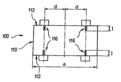
上記のような構成において、Nλg/2に等しい装置100の長さを短縮させるために、本発明の別の形態では、図示した第1の構造のように、λg/2おきに導波管110の長辺112の軸線の両側に2つのアンテナ116を設置する。
【0042】
g0を、軸線上のアンテナ116のコンダクタンスとした場合、導波管110の長辺112の軸線からの距離dにおける値gは、次の式で示される。
【0043】
g=g0cos2(πd/a) (3)
【0044】
更に、装置100の長さを短縮させるため、本発明の別の相補的形態は、先の構造のように、互いに対抗するようにアンテナ116の対を設ける。この場合、各対は、図3に略図で示すように、導波管110の長辺112の2つの面に設けられる。
【0045】
しかしながら、この選択案は、対抗するアンテナ116が接触してはならず、更に互いに過度に接近してはならず、対抗するアンテナ116間で相互作用が生じる結果、各アンテナ116のコンダクタンスが増加するために、得られるコンダクタンスの点で制約される。
【0046】
反射平面130を備える方形導波管110に基づく上記構造とは別に、アンテナ116を備えた方形導波管110の部分をリング共振器内に挿入することが可能である。この場合、共振器が(進行波モードではなく)定在波モードで作動し、移相器によりリング内のマイクロ波の電界最大点が電気結合アンテナ116の位置に対応することを保証するように、共振器を配置することが望ましい。
【0047】
本発明の別の形態では、導波管を介し、プラズマソース400に電力を伝達する用途に関連し、スロットを介して導波管から電力を取り出す。
【0048】
本発明の第2要素200は、各プラズマソース400に対して反射を生じることなく、独立して電力を伝達することを保証するようになっている。このことは、分割導波管110のアンテナ116の出力端とアプリケータとの間に、単一方向性アイソレータ200を挿入することによって達成される。
【0049】
このアイソレータは、一般に、フェライトをベースとする3分岐サーキュレータ210から成り、このサーキュレータ210は、プラズマソース400から来るすべての反射電力を吸収するようになっているマッチングされた負荷212によって、その第3分岐で終端している。この装置が正しく作動するために、分岐間のアイソレーションを、ほぼ20dBよりも大きくする必要がある。
【0050】
本発明の第3要素300は、こうして得られる電力が条件に従い、プラズマ内で多少とも完全に吸収されることを、各プラズマソース400に対するインピーダンスマッチングが保証できるようにしている。このことは、従来のインピーダンスマッチング装置、例えばトロンボーンライン、または3つのプランジャーを有するシステムを利用することによって達成できる。
【0051】
これら種々の使用可能な装置に必要とされる本質的な特徴は、インピーダンスマッチングの虚数部分および実数部分の双方に作用できることである。これにより、所望するプラズマ条件(密度、長さなど)に従って、ソース400のインピーダンスマッチングを調節できるようになる。
【0052】
図4には、本発明にかかわる代表的な電力分割装置の全体が略図で示されているマイクロ波発生器10(およびオプションとして、その保護用サーキュレータ)の後で、この電力分割装置は可動ショート回路130を備えた電力分割器100と、各プラズマソース400への電力伝達ラインとを含んでいる。各伝達ラインはプラズマソース400の上流側に設けられたインピーダンスマッチング装置300と共に、サーキュレータ210および(反射電力を吸収する)マッチングのとられた負荷212を有する。
【0053】
本発明にかかわる装置の主な利点は、単一のマイクロ波発生器10から、かなりの数のプラズマソース400にマイクロ波を供給できることである。更にこの装置は、簡単な要素から製造でき、これら要素のいくつかは、現在市販されているものである。
【0054】
本発明の装置は、どのタイプのマイクロ波アプリケータでも使用できる。
本明細書に開示した本発明の基本的な利点は、任意の数Nのアンテナ116にわたって、マイクロ波電力を分配できることであり、Nは奇数でもよい。
【0055】
本発明により、他のプラズマラインの作動を損なうことなく、1つ以上のプラズマラインを取り除くことが可能である。
【0056】
種々のプラズマソース400に対する供給手段の間の干渉を防止する本発明により、各プラズマソース400に対し、短時間でインピーダンスマッチングを行うことが可能である。
【0057】
最後に、本発明によれば、特にコンパクトな装置を製造することが可能である。
本発明を示す特定の限定的でない応用例として、導波管110の長辺112が幅A=86mm(導波管の短辺の幅b=43mmを有するWR340方形導波管規格を使って、電力を24分割するための装置(図5に略図で示されている)が挙げられる。
【0058】
2.45GHzでは、真空内の波長λ0=122.45mmであり、導波管内の波長(式1)は、次のとおりである。
【0059】
λg=174.4mm (4)
【0060】
この結果、アンテナ116またはアンテナのグループは、λg/2ごとに、すなわち87.2mmごとに、導波管110に沿って位置する。
N=24で分割するためのアンテナ11の正規化コンダクタンスg(式2)は、次の関係を必要とする。
【0061】
g=0.0417 (5)
【0062】
導波管の長辺の軸線からの距離d=26mmに対し、式(3)で示される導波管の長辺の軸線(D=0)におかれた同じ長さLのアンテナ116の対応するコンダクタンスg0は、次のように示される。
【0063】
g0=0.123 (6)
【0064】
実験で決定される長さLのアンテナ116の正規化インピーダンスg 0が、図1に示されている。式(6)によって示されるインピーダンス値に対応するアンテナの長さは、ほぼ次のとおりである(図1)。
【0065】
L 12.75mm (7)
【0066】
従って、こうして製造される、図5に略示するような、24分割用の電力分割器100は比較的コンパクトである。その理由は、全長が半波長の5倍(+アンテナの出力ポート、およびそれらの同軸コネクタに必要とされる空間)に対応するからである。
当然ながら、分割器100からの24本の伝達ラインの各々は、マッチングされた負荷212を備えるアイソレータ200と、プラズマソース400の上流側のインピーダンスマッチング300とを含む。
【0067】
プラズマの外側で、本発明にかかわる装置は、マイクロ波電力分割器によって別々に給電されるN個のアプリケータのうちの1つ以上で、インピーダンス変動が生じ得る任意のプロセスで使用できる。
【0068】
当然ながら、本発明は、これまでに説明した特定の実施例だけに限定されるものでなく、本発明の要旨に従って任意の変形例にも拡張できる。
【0069】
例えば、変形例として、導波管の長辺の軸線に対して対称的でない配置のアンテナを提供することも可能である。
【図面の簡単な説明】
【図1】 導波管内のこのアンテナの長さを関数とする導波管の入力端に戻されるアンテナの正規化コンダクタンスの変化を示す。
【図2】 導波管上の出力ポートまたはアンテナの別の形態を示す横断面図である。
【図3】 導波管上の出力ポートまたはアンテナの別の形態を示す横断面図である。
【図4】 本発明に係わる装置の全体の略図を示す。
【図5】 本発明の好ましい実施例に対応する斜視図である。
【符号の説明】
10−−マイクロ波発生器
100−−電力分割器
110−−導波管
112−−長辺
116−−アンテナ
130−−反射平面
212−−マッチングされた負荷
210−−サーキュレータ
300−−インピーダンス装置
400−−プラズマソース[0001]
The present invention relates to the technical field of microwave devices.
[0002]
More particularly, the present invention relates to the technical field of devices including several microwave sources supplied from a common microwave generator.
[0003]
The application of the present invention is in particular to generate plasma from a predetermined number of individual plasma sources that are fed with microwave power from a single power generator.
[0004]
These individual plasma sources may be independent in the same chamber (the purpose is to overcome physical or technical limitations on the maximum microwave power that can be applied to a single plasma source, for example). Also, it may be distributed in the same chamber so that the scale required for the intended application can be increased.
[0005]
In general, multi-plasma source applications not only cover all already covered areas by using a single plasma source, but also an integral plasma (eg for uniformity, rate, etc.) It can also cover new areas that are not possible with the source.
[0006]
The invention relates to all microwave plasmas and discharges, regardless of pressure range, microwave frequency, nature or configuration of the microwave applicator, and whether a magnetic field is present.
[0007]
However, the present invention is not limited to the technical field of plasma, but can also be applied to bonding, drying or curing operations using, for example, a multi-station. More generally, it can be applied to any work in which the system impedance varies from station to station.
[0008]
The microwave technology field is the subject of extensive research.
[0009]
Several proposals have been made to supply several plasma sources from a common plasma generator.
[0010]
In order to split the microwave power delivered from a single plasma generator, it is possible to use a cascade of 3 dB couplers (divided in two) formed, for example, from rectangular waveguides.
[0011]
This solution requires very large space, but allows the power to be divided by N = 2k, where k indicates the number of consecutive levels in the cascade. Therefore, the microwave power can be divided by a number such as 2, 4, 8, 16, 32, and the like. Matched coaxial / waveguide transitions at the end of each waveguide also allow microwave power to be carried by a coaxial cable fitted with a standard connector.
[0012]
Another widely implemented solution is to extract microwave power to either the cavity or waveguide, or ring resonator, and in the cavity, waveguide, or ring resonator, the electric field wave A standing wave is generated by the antenna installed in the rear (maximum electric field region).
[0013]
This solution assumes that each individual plasma source acts as a matched impedance. That is, it is assumed that the plasma source absorbs all of the extracted microwave power. When such a source is used, a predetermined microwave power can be sent to each individual microwave source.
[0014]
However, the conventionally proposed apparatus is not completely satisfactory.
[0015]
One problem in dividing microwave power to power the plasma source is that the plasma source typically does not operate as a matched load. The reason for this is that the impedance returned to the input of the plasma source generally corresponds to a matched load, resulting from the combination of the input impedance of the applicator and the impedance of the plasma returned to the input of the plasma source. That is, it does not match a pure resistive load equal to the characteristic impedance of the microwave supply line.
[0016]
On the other hand, the problem is that the impedance value varies from zero to infinite depending on the type of discharge, discharge conditions, and absorbed power, as well as the complex impedance value at the input of the plasma source.
[0017]
In the case of feeding several plasma sources from the same microwave generator, if there is not enough decoupling between the supply lines for the various microwave sources (typically> 20 dB), There is also the problem that impedance affects all other plasma sources.
[0018]
Therefore, immediately after firing, the input impedance of the plasma source is generally much larger than the corresponding input impedance when the discharge is in a steady state. Apart from this variation of impedance for a given plasma source at the moment of ignition, the power distribution is also influenced by various plasma sources that are not simultaneously ignited. Therefore, when turning on a large number of plasma sources, there is always a problem that a large imbalance of the power sent to the plasma sources occurs or a large amount of power is reflected in the circuit.
[0019]
These power imbalances, which cause the reflected power level to be very high, turn on the plasma, for example a surface wave plasma, in a plasma source that minimizes the plasma density and therefore the transmitted power must be minimized. To inhibit that.
[0020]
On the other hand, plasmas where the plasma density is limited to an upper limit, for example, the critical density, such as plasma using distributed electron cyclotron resonance, presents another problem related to impedance imbalance. . In this case, all incoming power greater than the value that guarantees the critical density is reflected at the input of the plasma source and returned to the microwave distribution circuit.
[0021]
In addition, intentional or unintentional variations in operating conditions (plasma gas composition, flow rate, pressure, density, radio frequency bias, etc.) occur, for example, when one of the plasma sources fails or during a multi-sequence process. After that, impedance imbalance may occur during operation.
[0022]
Finally, when several plasma sources are operating in the same chamber, interference between applicators can result in the reflected power level disturbing the desired power distribution.
[0023]
Thus, previous solutions for splitting microwave power are either excessively bulky (using a 3 dB coupler cascade), or only allowed to be split by a predetermined number N = 2k , or Although impedance matching is required, this was not possible in the case of using a plasma source.
[0024]
The object of the present invention is to improve a microwave system comprising several individual plasma sources supplied from a common plasma generator so as to eliminate the disadvantages of the prior art.
[0025]
This purpose is combined with a microwave generator and means coupled to said microwave generator and matched to operate in fundamental mode (H10) or transverse electrical mode (TE10) to ensure standing wave conditions. And a plurality of power output ports installed in the waveguide within the maximum amplitude region of one of the electromagnetic field components so as to divide the power with respect to the microwave generator. The power output port is adjusted so that the sum of normalized admittance y returned to the input end of the power divider formed by the rectangular waveguide is 1 unit, and the power is reflected to the output port. Located downstream of the isolator means between the isolator means and the associated source to ensure power transfer from the output port to the source without returning This is achieved by the system of the present invention comprising a plurality of sources each coupled to an output port of the waveguide, with an apparatus for matching the impedance of each source.
[0026]
Other features, objects and advantages of the present invention will become apparent from the following detailed description, taken in conjunction with the accompanying drawings, shown by way of non-limiting example.
[0027]
As described above, the present invention includes three elements: a
[0028]
More specifically, according to the present invention, a
This wavelength λ g satisfies the following equation.
[0029]
1 / λ g 2 = 1 / λ 0 2 −1 / (2a) 2 (1)
[0030]
Here, a is the width of the
[0031]
In order to perform the necessary power division, for example, on the side opposite to the microwave power feeding point from the
[0032]
Accordingly, in the present invention, the
[0033]
In the case where electric power is taken out by the electric antenna, it is preferable to install the
[0034]
In the case where electric power is taken out by the magnetic antenna 116 (loop), it is necessary to provide the
[0035]
To ensure that the total impedance generated at the input of the
[0036]
To obtain such results, the depth of penetration of the
[0037]
As an example, in the case of dividing the microwave power equally N ways using electrical coupling, the normalized conductance (relative to the characteristic impedance) of the antenna 11 returned to the input end of the waveguide is It is shown by the formula of
[0038]
g = 1 / N (2)
[0039]
Thus, for a given shape and a given diameter, the length of
[0040]
FIG. 1 shows an antenna for an antenna along one axis of the
[0041]
In such a configuration, in order to reduce the length of the
[0042]
When g 0 is the conductance of the
[0043]
g = g 0 cos 2 (πd / a) (3)
[0044]
Furthermore, to reduce the length of the
[0045]
However, this alternative is not to allow the opposing
[0046]
Apart from the above structure based on the
[0047]
In another form of the invention, power is drawn from the waveguide through the slot in connection with applications that transfer power to the
[0048]
The
[0049]
The isolator generally consists of a ferrite-based three-
[0050]
The
[0051]
An essential feature required for these various usable devices is that they can act on both the imaginary and real parts of impedance matching. Thereby, the impedance matching of the
[0052]
In FIG. 4, after the microwave generator 10 (and optionally its protective circulator), which is schematically shown in its entirety, an exemplary power divider according to the present invention is shown as a movable short circuit. It includes a
[0053]
The main advantage of the apparatus according to the invention is that a
[0054]
The device of the present invention can be used with any type of microwave applicator.
A fundamental advantage of the invention disclosed herein is that microwave power can be distributed over any number N of
[0055]
The present invention makes it possible to remove one or more plasma lines without compromising the operation of other plasma lines.
[0056]
According to the present invention for preventing interference between supply means for
[0057]
Finally, according to the invention, it is possible to produce a particularly compact device.
As a specific non-limiting application illustrating the present invention, using the WR340 rectangular waveguide standard where the
[0058]
At 2.45 GHz, the wavelength λ 0 in the vacuum is 122.45 mm, and the wavelength in the waveguide (Equation 1) is as follows.
[0059]
λ g = 174.4 mm (4)
[0060]
As a result, the
The normalized conductance g (Equation 2) of the antenna 11 for dividing by N = 24 requires the following relationship.
[0061]
g = 0.0417 (5)
[0062]
Correspondence of the
[0063]
g 0 = 0.123 (6)
[0064]
Normalization impedance g 0 of the
[0065]
L 12.75mm (7)
[0066]
Therefore, the 24-divided
Of course, each of the 24 transmission lines from the
[0067]
Outside the plasma, the device according to the invention can be used in any process where impedance variations can occur in one or more of the N applicators that are separately powered by a microwave power divider.
[0068]
Of course, the present invention is not limited to the specific embodiments described so far and can be extended to any variant according to the gist of the present invention.
[0069]
For example, as a modification, it is possible to provide an antenna having an arrangement that is not symmetrical with respect to the long axis of the waveguide.
[Brief description of the drawings]
FIG. 1 shows the change in normalized conductance of an antenna returned to the input end of the waveguide as a function of the length of this antenna in the waveguide.
FIG. 2 is a cross-sectional view showing another form of output port or antenna on the waveguide.
FIG. 3 is a cross-sectional view showing another form of output port or antenna on the waveguide.
FIG. 4 shows a schematic diagram of the entire apparatus according to the present invention.
FIG. 5 is a perspective view corresponding to a preferred embodiment of the present invention.
[Explanation of symbols]
10--
Claims (16)
前記マイクロ波発生器(10)に結合され、基本モード(H10)または横電気モード(TE10)で作動するようにマッチングされ、定在波条件を保証する手段と組み合わされた方形の導波管(110)と、
マイクロ波発生器(10)に対し、電力分割をするように電磁界成分のうちの1つの成分の最大振幅領域内にて前記導波管(110)内に設置された複数の電力出力ポート(116)とを備え、前記導波管(110)によって形成された電力分割器の入力端に戻される正規化アドミッタンスyの和が1単位となるように、前記電力出力ポート(116)が調整されており、
出力ポート(116)に電力を反射して戻すことなく、出力ポート(116)からソース(400)までの電力伝達を保証するアイソレータ手段(200)、および
アイソレータ手段(200)と関連するソース(400)との間において、アイソレータ手段(200)の下流側に位置する、各ソース(400)のインピーダンスをマッチングするための装置(300)により、
前記導波管(110)の出力ポート(116)にそれぞれ結合された複数のソース(400)とを備え、
該正規化アドミッタンスyは、正規化インピーダンスの逆数により与えられ、該正規化インピーダンスは、インピーダンスの測定値を特性インピーダンスで除して得られるものであることを特徴とするマイクロ波システム。A microwave generator (10);
A rectangular waveguide coupled to the microwave generator (10), matched to operate in the fundamental mode (H10) or transverse electrical mode (TE10), and combined with means to ensure standing wave conditions ( 110)
Microwave generator to (10), a plurality of power output ports placed in the waveguide (110) at a maximum of one component of the electromagnetic field component amplitude region to the power splitting ( 116) and wherein the such that the sum of the normalized admittance y returned to the input end of the power divider formed by the waveguide (110) is one unit, the power output port (116) is adjusted And
Isolator means (200) that ensures power transfer from output port (116) to source (400) without reflecting power back to output port (116), and source (400) associated with isolator means (200) ) With a device (300) for matching the impedance of each source (400) located downstream of the isolator means (200),
A plurality of the source (400) coupled to the output port (116) of the waveguide (110),
The microwave admittance y is given by a reciprocal of a normalized impedance, and the normalized impedance is obtained by dividing a measured impedance value by a characteristic impedance.
Applications Claiming Priority (3)
| Application Number | Priority Date | Filing Date | Title |
|---|---|---|---|
| FR9911422A FR2798552B1 (en) | 1999-09-13 | 1999-09-13 | DEVICE FOR PROVIDING A PREDETERMINED MICROWAVE POWER DIVISION ON A PLURALITY OF LOADS, PARTICULARLY FOR THE PRODUCTION OF PLASMA |
| FR99/11422 | 1999-09-13 | ||
| PCT/FR2000/002507 WO2001020710A1 (en) | 1999-09-13 | 2000-09-12 | Power splitter for plasma device |
Publications (3)
| Publication Number | Publication Date |
|---|---|
| JP2003509832A JP2003509832A (en) | 2003-03-11 |
| JP2003509832A5 JP2003509832A5 (en) | 2010-11-25 |
| JP4982022B2 true JP4982022B2 (en) | 2012-07-25 |
Family
ID=9549779
Family Applications (1)
| Application Number | Title | Priority Date | Filing Date |
|---|---|---|---|
| JP2001524184A Expired - Lifetime JP4982022B2 (en) | 1999-09-13 | 2000-09-12 | Microwave system |
Country Status (7)
| Country | Link |
|---|---|
| US (1) | US6727656B1 (en) |
| EP (1) | EP1216493B1 (en) |
| JP (1) | JP4982022B2 (en) |
| AT (1) | ATE245855T1 (en) |
| DE (1) | DE60004073T2 (en) |
| FR (1) | FR2798552B1 (en) |
| WO (1) | WO2001020710A1 (en) |
Families Citing this family (17)
| Publication number | Priority date | Publication date | Assignee | Title |
|---|---|---|---|---|
| JP4150621B2 (en) * | 2002-09-20 | 2008-09-17 | 富士通株式会社 | Foldable portable radio and chassis of the radio |
| US7445690B2 (en) * | 2002-10-07 | 2008-11-04 | Tokyo Electron Limited | Plasma processing apparatus |
| US7806077B2 (en) * | 2004-07-30 | 2010-10-05 | Amarante Technologies, Inc. | Plasma nozzle array for providing uniform scalable microwave plasma generation |
| US20070095281A1 (en) * | 2005-11-01 | 2007-05-03 | Stowell Michael W | System and method for power function ramping of microwave liner discharge sources |
| JP4862375B2 (en) * | 2005-12-06 | 2012-01-25 | 株式会社エーイーティー | Traveling waveform microwave plasma generator |
| JP6085413B2 (en) * | 2008-08-20 | 2017-02-22 | コーニンクレッカ フィリップス エヌ ヴェKoninklijke Philips N.V. | RF power splitter for magnetic resonance system |
| US20110094830A1 (en) * | 2009-10-26 | 2011-04-28 | Lund Kurt O'ferrall | Vehicle and object portable lift |
| GB201021853D0 (en) | 2010-12-23 | 2011-02-02 | Element Six Ltd | A microwave plasma reactor for manufacturing synthetic diamond material |
| GB201021865D0 (en) | 2010-12-23 | 2011-02-02 | Element Six Ltd | A microwave plasma reactor for manufacturing synthetic diamond material |
| GB201021870D0 (en) | 2010-12-23 | 2011-02-02 | Element Six Ltd | A microwave plasma reactor for manufacturing synthetic diamond material |
| GB201021913D0 (en) | 2010-12-23 | 2011-02-02 | Element Six Ltd | Microwave plasma reactors and substrates for synthetic diamond manufacture |
| GB201021855D0 (en) * | 2010-12-23 | 2011-02-02 | Element Six Ltd | Microwave power delivery system for plasma reactors |
| GB201021860D0 (en) | 2010-12-23 | 2011-02-02 | Element Six Ltd | A microwave plasma reactor for diamond synthesis |
| KR101481928B1 (en) | 2010-12-23 | 2015-01-21 | 엘리멘트 식스 리미티드 | Controlling doping of synthetic diamond material |
| FR2974701B1 (en) | 2011-04-27 | 2014-03-21 | Sairem Soc Pour L Applic Ind De La Rech En Electronique Et Micro Ondes | PRODUCTION PLANT FOR MICROWAVE PLASMA |
| WO2012161231A1 (en) * | 2011-05-24 | 2012-11-29 | イマジニアリング株式会社 | Electromagnetic wave emitting device |
| KR102007230B1 (en) * | 2018-01-26 | 2019-08-06 | 한국원자력연구원 | Variable High Power RF divider |
Citations (7)
| Publication number | Priority date | Publication date | Assignee | Title |
|---|---|---|---|---|
| JPS5946553U (en) * | 1982-09-20 | 1984-03-28 | オージー技研株式会社 | microwave therapy device |
| JPS61290722A (en) * | 1985-06-19 | 1986-12-20 | Tokuda Seisakusho Ltd | Plasma generator |
| JPH01132236U (en) * | 1988-03-02 | 1989-09-07 | ||
| JPH0339480A (en) * | 1989-07-05 | 1991-02-20 | Sony Corp | Ecr plasma device |
| JPH1140397A (en) * | 1997-05-22 | 1999-02-12 | Canon Inc | Microwave feeder having annular waveguide and plasma processing device provided with the microwave feeder and processing method |
| JPH1167492A (en) * | 1997-05-29 | 1999-03-09 | Sumitomo Metal Ind Ltd | Plasma treatment equipment and plasma treatment method |
| JPH11195924A (en) * | 1997-12-26 | 1999-07-21 | New Japan Radio Co Ltd | Micro-strip array antenna |
Family Cites Families (12)
| Publication number | Priority date | Publication date | Assignee | Title |
|---|---|---|---|---|
| JPS5946553A (en) * | 1982-09-08 | 1984-03-15 | Sumitomo Chem Co Ltd | Angle beam ultrasonic flaw inspection |
| DE3711184A1 (en) * | 1987-04-02 | 1988-10-20 | Leybold Ag | DEVICE FOR THE APPLICATION OF MICROWAVE ENERGY WITH AN OPEN MICROWAVE LEAD |
| JPH01132236A (en) * | 1987-11-18 | 1989-05-24 | Matsushita Electric Ind Co Ltd | Parts fixing method |
| US5153406A (en) * | 1989-05-31 | 1992-10-06 | Applied Science And Technology, Inc. | Microwave source |
| JPH0441675A (en) * | 1990-06-07 | 1992-02-12 | Matsushita Electric Ind Co Ltd | Microwave plasma device |
| DE4235914A1 (en) * | 1992-10-23 | 1994-04-28 | Juergen Prof Dr Engemann | Device for generating microwave plasmas |
| US5714009A (en) * | 1995-01-11 | 1998-02-03 | Deposition Sciences, Inc. | Apparatus for generating large distributed plasmas by means of plasma-guided microwave power |
| US5796080A (en) * | 1995-10-03 | 1998-08-18 | Cem Corporation | Microwave apparatus for controlling power levels in individual multiple cells |
| KR970071945A (en) * | 1996-02-20 | 1997-11-07 | 가나이 쯔도무 | Plasma treatment method and apparatus |
| US5869817A (en) * | 1997-03-06 | 1999-02-09 | General Mills, Inc. | Tunable cavity microwave applicator |
| US6258329B1 (en) * | 1998-04-20 | 2001-07-10 | Cem Corporation | Microwave transparent vessel for microwave assisted chemical processes |
| US6084226A (en) * | 1998-04-21 | 2000-07-04 | Cem Corporation | Use of continuously variable power in microwave assisted chemistry |
-
1999
- 1999-09-13 FR FR9911422A patent/FR2798552B1/en not_active Expired - Lifetime
-
2000
- 2000-09-12 WO PCT/FR2000/002507 patent/WO2001020710A1/en active IP Right Grant
- 2000-09-12 DE DE60004073T patent/DE60004073T2/en not_active Expired - Lifetime
- 2000-09-12 AT AT00962606T patent/ATE245855T1/en not_active IP Right Cessation
- 2000-09-12 EP EP00962606A patent/EP1216493B1/en not_active Expired - Lifetime
- 2000-09-12 JP JP2001524184A patent/JP4982022B2/en not_active Expired - Lifetime
- 2000-09-12 US US10/088,326 patent/US6727656B1/en not_active Expired - Lifetime
Patent Citations (7)
| Publication number | Priority date | Publication date | Assignee | Title |
|---|---|---|---|---|
| JPS5946553U (en) * | 1982-09-20 | 1984-03-28 | オージー技研株式会社 | microwave therapy device |
| JPS61290722A (en) * | 1985-06-19 | 1986-12-20 | Tokuda Seisakusho Ltd | Plasma generator |
| JPH01132236U (en) * | 1988-03-02 | 1989-09-07 | ||
| JPH0339480A (en) * | 1989-07-05 | 1991-02-20 | Sony Corp | Ecr plasma device |
| JPH1140397A (en) * | 1997-05-22 | 1999-02-12 | Canon Inc | Microwave feeder having annular waveguide and plasma processing device provided with the microwave feeder and processing method |
| JPH1167492A (en) * | 1997-05-29 | 1999-03-09 | Sumitomo Metal Ind Ltd | Plasma treatment equipment and plasma treatment method |
| JPH11195924A (en) * | 1997-12-26 | 1999-07-21 | New Japan Radio Co Ltd | Micro-strip array antenna |
Also Published As
| Publication number | Publication date |
|---|---|
| FR2798552A1 (en) | 2001-03-16 |
| ATE245855T1 (en) | 2003-08-15 |
| DE60004073D1 (en) | 2003-08-28 |
| EP1216493B1 (en) | 2003-07-23 |
| DE60004073T2 (en) | 2004-04-15 |
| WO2001020710A1 (en) | 2001-03-22 |
| JP2003509832A (en) | 2003-03-11 |
| US6727656B1 (en) | 2004-04-27 |
| FR2798552B1 (en) | 2001-11-30 |
| EP1216493A1 (en) | 2002-06-26 |
Similar Documents
| Publication | Publication Date | Title |
|---|---|---|
| JP4982022B2 (en) | Microwave system | |
| US5892414A (en) | Dielectric waveguide power combiner | |
| JP3162403B2 (en) | Millimeter-wave band mixer using window processing technology | |
| US4491810A (en) | Multi-port, multi-frequency microwave combiner with overmoded square waveguide section | |
| US7186314B2 (en) | Plasma processor and plasma processing method | |
| KR20030072343A (en) | Feeding of microwave | |
| WO2006033278A1 (en) | Magnetron oscillation device | |
| JP3957135B2 (en) | Plasma processing equipment | |
| US6888115B2 (en) | Cascaded planar exposure chamber | |
| US2975381A (en) | Duplexers | |
| US4091334A (en) | Connection of a plurality of devices to a circular waveguide | |
| US3324423A (en) | Dual waveguide mode source having control means for adjusting the relative amplitudesof two modes | |
| US2769145A (en) | Microwave power divider | |
| US5280217A (en) | Apparatus for coupling energy to electrodeless lamp applicators | |
| US2930004A (en) | Microwave pulser | |
| US2714707A (en) | Circular polarizer | |
| JP3129814B2 (en) | Microwave plasma device | |
| US3221276A (en) | Microwave variable reactance device operating about a resonant condition | |
| Garcia et al. | High performance of dual band/dual polarization compact OMT | |
| JPH07226609A (en) | Directional coupler | |
| Zakrzewski et al. | Surface-wave plasma sources | |
| He et al. | Development of a high-power high-directivity directional coupler and four power dividers for S-band | |
| KR100401128B1 (en) | The High Power Divider/Combiner With Center Frequency Shifting Characteristics | |
| JP3878267B2 (en) | Plasma processing equipment | |
| Katalev et al. | Waveguide distribution systems for the European XFEL |
Legal Events
| Date | Code | Title | Description |
|---|---|---|---|
| A621 | Written request for application examination |
Free format text: JAPANESE INTERMEDIATE CODE: A621 Effective date: 20070719 |
|
| A977 | Report on retrieval |
Free format text: JAPANESE INTERMEDIATE CODE: A971007 Effective date: 20100329 |
|
| A131 | Notification of reasons for refusal |
Free format text: JAPANESE INTERMEDIATE CODE: A131 Effective date: 20100406 |
|
| A601 | Written request for extension of time |
Free format text: JAPANESE INTERMEDIATE CODE: A601 Effective date: 20100629 |
|
| A602 | Written permission of extension of time |
Free format text: JAPANESE INTERMEDIATE CODE: A602 Effective date: 20100706 |
|
| A521 | Request for written amendment filed |
Free format text: JAPANESE INTERMEDIATE CODE: A523 Effective date: 20101006 |
|
| A524 | Written submission of copy of amendment under article 19 pct |
Free format text: JAPANESE INTERMEDIATE CODE: A524 Effective date: 20101006 |
|
| A131 | Notification of reasons for refusal |
Free format text: JAPANESE INTERMEDIATE CODE: A131 Effective date: 20110524 |
|
| A601 | Written request for extension of time |
Free format text: JAPANESE INTERMEDIATE CODE: A601 Effective date: 20110815 |
|
| A602 | Written permission of extension of time |
Free format text: JAPANESE INTERMEDIATE CODE: A602 Effective date: 20110822 |
|
| A711 | Notification of change in applicant |
Free format text: JAPANESE INTERMEDIATE CODE: A711 Effective date: 20111026 |
|
| A521 | Request for written amendment filed |
Free format text: JAPANESE INTERMEDIATE CODE: A821 Effective date: 20111026 |
|
| A521 | Request for written amendment filed |
Free format text: JAPANESE INTERMEDIATE CODE: A523 Effective date: 20111124 |
|
| A131 | Notification of reasons for refusal |
Free format text: JAPANESE INTERMEDIATE CODE: A131 Effective date: 20111220 |
|
| A521 | Request for written amendment filed |
Free format text: JAPANESE INTERMEDIATE CODE: A523 Effective date: 20120308 |
|
| TRDD | Decision of grant or rejection written | ||
| A01 | Written decision to grant a patent or to grant a registration (utility model) |
Free format text: JAPANESE INTERMEDIATE CODE: A01 Effective date: 20120403 |
|
| A01 | Written decision to grant a patent or to grant a registration (utility model) |
Free format text: JAPANESE INTERMEDIATE CODE: A01 |
|
| A61 | First payment of annual fees (during grant procedure) |
Free format text: JAPANESE INTERMEDIATE CODE: A61 Effective date: 20120423 |
|
| FPAY | Renewal fee payment (event date is renewal date of database) |
Free format text: PAYMENT UNTIL: 20150427 Year of fee payment: 3 |
|
| R150 | Certificate of patent or registration of utility model |
Ref document number: 4982022 Country of ref document: JP Free format text: JAPANESE INTERMEDIATE CODE: R150 Free format text: JAPANESE INTERMEDIATE CODE: R150 |
|
| A524 | Written submission of copy of amendment under article 19 pct |
Free format text: JAPANESE INTERMEDIATE CODE: A524 Effective date: 20101006 |
|
| R250 | Receipt of annual fees |
Free format text: JAPANESE INTERMEDIATE CODE: R250 |
|
| R250 | Receipt of annual fees |
Free format text: JAPANESE INTERMEDIATE CODE: R250 |
|
| R250 | Receipt of annual fees |
Free format text: JAPANESE INTERMEDIATE CODE: R250 |
|
| R250 | Receipt of annual fees |
Free format text: JAPANESE INTERMEDIATE CODE: R250 |
|
| R250 | Receipt of annual fees |
Free format text: JAPANESE INTERMEDIATE CODE: R250 |
|
| R250 | Receipt of annual fees |
Free format text: JAPANESE INTERMEDIATE CODE: R250 |
|
| EXPY | Cancellation because of completion of term |