JP4963375B2 - Optical device, optical member and light guide - Google Patents
Optical device, optical member and light guide Download PDFInfo
- Publication number
- JP4963375B2 JP4963375B2 JP2006155613A JP2006155613A JP4963375B2 JP 4963375 B2 JP4963375 B2 JP 4963375B2 JP 2006155613 A JP2006155613 A JP 2006155613A JP 2006155613 A JP2006155613 A JP 2006155613A JP 4963375 B2 JP4963375 B2 JP 4963375B2
- Authority
- JP
- Japan
- Prior art keywords
- optical member
- optical
- film
- light
- protective medium
- Prior art date
- Legal status (The legal status is an assumption and is not a legal conclusion. Google has not performed a legal analysis and makes no representation as to the accuracy of the status listed.)
- Active
Links
- 230000003287 optical effect Effects 0.000 title claims description 233
- 239000013307 optical fiber Substances 0.000 claims description 67
- 230000001681 protective effect Effects 0.000 claims description 42
- KRHYYFGTRYWZRS-UHFFFAOYSA-M Fluoride anion Chemical compound [F-] KRHYYFGTRYWZRS-UHFFFAOYSA-M 0.000 claims description 15
- 239000000463 material Substances 0.000 claims description 11
- 229910004261 CaF 2 Inorganic materials 0.000 claims description 9
- 238000004140 cleaning Methods 0.000 claims description 9
- 230000010355 oscillation Effects 0.000 claims description 9
- 229910016036 BaF 2 Inorganic materials 0.000 claims description 8
- 229910017768 LaF 3 Inorganic materials 0.000 claims description 8
- 229910016569 AlF 3 Inorganic materials 0.000 claims description 7
- PUZPDOWCWNUUKD-UHFFFAOYSA-M sodium fluoride Inorganic materials [F-].[Na+] PUZPDOWCWNUUKD-UHFFFAOYSA-M 0.000 claims description 6
- 239000010408 film Substances 0.000 description 231
- 238000000034 method Methods 0.000 description 25
- 238000006243 chemical reaction Methods 0.000 description 21
- 239000010410 layer Substances 0.000 description 17
- 238000007740 vapor deposition Methods 0.000 description 11
- 150000002500 ions Chemical class 0.000 description 10
- 238000010521 absorption reaction Methods 0.000 description 9
- 239000011521 glass Substances 0.000 description 9
- 239000000126 substance Substances 0.000 description 8
- 230000007423 decrease Effects 0.000 description 7
- 239000000835 fiber Substances 0.000 description 7
- 229910004298 SiO 2 Inorganic materials 0.000 description 6
- 239000010453 quartz Substances 0.000 description 6
- VYPSYNLAJGMNEJ-UHFFFAOYSA-N silicon dioxide Inorganic materials O=[Si]=O VYPSYNLAJGMNEJ-UHFFFAOYSA-N 0.000 description 6
- 230000015572 biosynthetic process Effects 0.000 description 4
- 230000000694 effects Effects 0.000 description 3
- 239000012528 membrane Substances 0.000 description 3
- 238000005498 polishing Methods 0.000 description 3
- 239000002356 single layer Substances 0.000 description 3
- 238000011109 contamination Methods 0.000 description 2
- 238000000151 deposition Methods 0.000 description 2
- 238000002845 discoloration Methods 0.000 description 2
- 238000007733 ion plating Methods 0.000 description 2
- 238000000869 ion-assisted deposition Methods 0.000 description 2
- 238000004544 sputter deposition Methods 0.000 description 2
- 230000003746 surface roughness Effects 0.000 description 2
- 230000002123 temporal effect Effects 0.000 description 2
- 239000004809 Teflon Substances 0.000 description 1
- 229920006362 Teflon® Polymers 0.000 description 1
- 239000000853 adhesive Substances 0.000 description 1
- 230000001070 adhesive effect Effects 0.000 description 1
- 230000008021 deposition Effects 0.000 description 1
- 238000010586 diagram Methods 0.000 description 1
- 238000002474 experimental method Methods 0.000 description 1
- 230000004927 fusion Effects 0.000 description 1
- 230000010354 integration Effects 0.000 description 1
- 238000001659 ion-beam spectroscopy Methods 0.000 description 1
- 238000010884 ion-beam technique Methods 0.000 description 1
- 238000005304 joining Methods 0.000 description 1
- 238000005259 measurement Methods 0.000 description 1
- 239000005416 organic matter Substances 0.000 description 1
- 238000000926 separation method Methods 0.000 description 1
- 239000010409 thin film Substances 0.000 description 1
Images


Classifications
-
- G—PHYSICS
- G02—OPTICS
- G02B—OPTICAL ELEMENTS, SYSTEMS OR APPARATUS
- G02B6/00—Light guides; Structural details of arrangements comprising light guides and other optical elements, e.g. couplings
- G02B6/24—Coupling light guides
-
- G—PHYSICS
- G02—OPTICS
- G02B—OPTICAL ELEMENTS, SYSTEMS OR APPARATUS
- G02B6/00—Light guides; Structural details of arrangements comprising light guides and other optical elements, e.g. couplings
- G02B6/24—Coupling light guides
- G02B6/26—Optical coupling means
- G02B6/262—Optical details of coupling light into, or out of, or between fibre ends, e.g. special fibre end shapes or associated optical elements
-
- G—PHYSICS
- G02—OPTICS
- G02B—OPTICAL ELEMENTS, SYSTEMS OR APPARATUS
- G02B6/00—Light guides; Structural details of arrangements comprising light guides and other optical elements, e.g. couplings
- G02B6/24—Coupling light guides
- G02B6/255—Splicing of light guides, e.g. by fusion or bonding
-
- G—PHYSICS
- G02—OPTICS
- G02B—OPTICAL ELEMENTS, SYSTEMS OR APPARATUS
- G02B6/00—Light guides; Structural details of arrangements comprising light guides and other optical elements, e.g. couplings
- G02B6/24—Coupling light guides
- G02B6/26—Optical coupling means
- G02B6/32—Optical coupling means having lens focusing means positioned between opposed fibre ends
-
- G—PHYSICS
- G02—OPTICS
- G02B—OPTICAL ELEMENTS, SYSTEMS OR APPARATUS
- G02B6/00—Light guides; Structural details of arrangements comprising light guides and other optical elements, e.g. couplings
- G02B6/24—Coupling light guides
- G02B6/36—Mechanical coupling means
-
- G—PHYSICS
- G02—OPTICS
- G02B—OPTICAL ELEMENTS, SYSTEMS OR APPARATUS
- G02B6/00—Light guides; Structural details of arrangements comprising light guides and other optical elements, e.g. couplings
- G02B6/24—Coupling light guides
- G02B6/42—Coupling light guides with opto-electronic elements
- G02B6/4201—Packages, e.g. shape, construction, internal or external details
- G02B6/4204—Packages, e.g. shape, construction, internal or external details the coupling comprising intermediate optical elements, e.g. lenses, holograms
- G02B6/421—Packages, e.g. shape, construction, internal or external details the coupling comprising intermediate optical elements, e.g. lenses, holograms the intermediate optical component consisting of a short length of fibre, e.g. fibre stub
Landscapes
- Physics & Mathematics (AREA)
- General Physics & Mathematics (AREA)
- Optics & Photonics (AREA)
- Engineering & Computer Science (AREA)
- Plasma & Fusion (AREA)
- Optical Couplings Of Light Guides (AREA)
- Mechanical Coupling Of Light Guides (AREA)
Description
本発明は、2本の光学部材又はライトガイドの端部がスリーブ等の保持部材によって保持された光デバイス、又は外部光学部材と組み合わせて使用するライトガイド及び光学部材に関するものである。 The present invention relates to a light guide and an optical member used in combination with an optical device in which ends of two optical members or light guides are held by a holding member such as a sleeve, or an external optical member.
スリーブ等の保持部材を用いて2本の光ファイバの端部を接続する当接方法として、一般的にオプティカルコンタクトが用いられる。オプティカルコンタクトとは、光ファイバ等の光学部品を接着剤等の媒体を介さずに直接圧着して当接する方法であり、一般的には光学部材同士を直接当接する為、光伝播効率が高い方法である。図7に従来の光デバイス100の断面図を示す。図7に示すように、光ファイバ1aはフェルール2aに挿入されることにより、光ファイバ1bはフェルール2bに挿入されることにより保持され、更にフェルール2a及び2bの一端がスリーブ3に挿入されることによって固定される。フェルール2a及び2bのスリーブ3に挿入される側の端部は研磨によって例えば半球面状に研磨される。半球面状に研磨されることによって、光ファイバ1a、1bの端部同士を密着させやすくなり、安定的で低損失な接続を得ることができる。また、光学部品の安定的なオプティカルコンタクトについては、特許文献1〜3にも記載されている。
上記したような光デバイスにおいて、特に短波長領域の光を光ファイバ1a及び1bに導波させる場合、有機物質による汚染が生じやすいため、それに伴う特性劣化を防ぐために、フェルール2a、2b(以下、包括的に「フェルール2」と表記する)に光ファイバ1a、1b(以下、包括的に「光ファイバ1」と表記する)を挿入して端部を研磨した後、該端部をUVクリーニング等することによって有機物質の除去を行う。
In the optical device as described above, in particular, when light in the short wavelength region is guided to the
しかしながら、UVクリーニングによって有機物質を除去し、光ファイバ1aと1bの端部を圧着させてオプティカルコンタクトさせると、光ファイバ1に含まれる酸化物(石英、SiO2等)が当接部において何らかの反応を起こして反応箇所が一体化し、その反応後にフェルール2をスリーブ3から抜くと、反応箇所が破損してしまうことが出願人によって確認された。
However, when organic substances are removed by UV cleaning and the ends of the
また、UVクリーニングがされても有機物質が若干除去し切れず、光ファイバ1の端部に残留したままオプティカルコンタクトにより短波長領域の光を光ファイバ1に導波させた場合、光ファイバ1aと1bの当接部における有機物質が該光によって分解されるため、上記したように光ファイバ1に含まれる酸化物が反応を起こして、光ファイバ1の当接部の破損を招いていた。光ファイバ1の当接部が破損すると、光損失が大きく増加し、所望の性能が得られなくなり、光デバイスとしての信頼性が低下してしまう。
Further, even when UV cleaning is performed, organic substances are not completely removed, and light in a short wavelength region is guided to the
本発明は、光ファイバの当接部における破損を抑え、高い信頼性を得られる光デバイス、ライトガイド及び光学部材を提供することを目的とする。 An object of the present invention is to provide an optical device, a light guide, and an optical member that can prevent damage at a contact portion of an optical fiber and obtain high reliability.
以上の課題を解決するために、本発明による光デバイスは、入射された光を出射端から出射する第1の光学部材と、該第1の光学部材の出射端から出射された光を該出射端に当接する入射端から入射する第2の光学部材とからなる光デバイスにおいて、前記第1の光学部材の出射端と前記第2の光学部材の入射端の間に、前記第1の光学部材と前記第2の光学部材の接着を抑止する保護媒体が配置されていることを特徴としている。 In order to solve the above-mentioned problems, an optical device according to the present invention includes a first optical member that emits incident light from an emission end, and the light emitted from the emission end of the first optical member. An optical device comprising a second optical member incident from an incident end abutting on the end, wherein the first optical member is disposed between an emission end of the first optical member and an incident end of the second optical member. And a protective medium for preventing adhesion of the second optical member.
ここで「前記第1の光学部材と前記第2の光学部材の接着を抑止する保護媒体」とは、2つの光学部材が常温で物理的に当接状態にあるときに、該光学部材の当接部における材料が化学反応を起こし、融着等によって接着されることを防ぐ保護媒体である。即ち、2つの光学部材を物理的に当接した後に該光学部材を離間させた際、又は光学部材を当接部から相対的に動かした際に、光学部材の当接部において発生した付着物(又は、付着物による表面凹凸)がλ/2以下(λ=光の発振波長)、より好ましくはλ/5以下、更に好ましくはλ/10以下となるように当接部の接着を抑止する保護媒体である。 Here, the “protective medium that inhibits the adhesion between the first optical member and the second optical member” means that when the two optical members are in physical contact with each other at room temperature, It is a protective medium that prevents the material in the contact portion from causing a chemical reaction and being adhered by fusion or the like. That is, deposits generated at the contact portion of the optical member when the two optical members are physically contacted and then separated from each other or when the optical member is moved relatively from the contact portion. Adhesion of the abutting portion is suppressed so that (or surface irregularities due to adhered matter) is λ / 2 or less (λ = oscillation wavelength of light), more preferably λ / 5 or less, and further preferably λ / 10 or less. It is a protective medium.
また「該第1の光学部材の出射端から出射された光を該出射端に当接する入射端から入射する第2の光学部材とからなる光デバイス」としたが、第1の光学部材の出射端と第2の光学部材の入射端とが接合部材等を用いて接合されてつなぎ合わせられたものであってもよい。 In addition, although “an optical device including a second optical member that is incident from an incident end that abuts the light exiting from the exit end of the first optical member” is described as an output from the first optical member. The end and the incident end of the second optical member may be joined and joined using a joining member or the like.
更に、本発明による光デバイスは、入射された光を出射端から出射する第1の光学部材と、該第1の光学部材の出射端から出射された光を該出射端に当接する入射端から入射する第2の光学部材とからなる光デバイスにおいて、前記第1の光学部材の出射端と前記第2の光学部材の入射端の間に、前記第1の光学部材と前記第2の光学部材とを500[g重]の荷重で当接させ、後に離間させても、前記出射端と前記入射端を再使用可能な状態に維持する透明な保護媒体が配置されていることを特徴としている。 Furthermore, an optical device according to the present invention includes a first optical member that emits incident light from an emission end, and an incident end that abuts the light emitted from the emission end of the first optical member. In the optical device comprising the incident second optical member, the first optical member and the second optical member are disposed between the exit end of the first optical member and the entrance end of the second optical member. Are disposed with a load of 500 [g weight], and a transparent protective medium is provided that maintains the output end and the input end in a reusable state even when they are separated later. .
また、前記荷重が、1[kg重]であることとしてもよい。更に「前記第1の光学部材と前記第2の光学部材とを500[g重]の荷重で当接させ」としたが、第1の光学部材と第2の光学部材とを接合部材等を用いて接合させてつなぎ合わせてもよい。その際も、当接部(即ち、接合部)において500[g重](又は1[kg重])の荷重で第1の光学部材と第2の光学部材とを接合させ、後に離間させても、第1の光学部材の出射端と第2の光学部材の入射端が再使用可能な状態に維持する透明な保護媒体が当接部(即ち、接合部)に配置されていることとする。 The load may be 1 [kg weight]. Furthermore, “the first optical member and the second optical member are brought into contact with each other with a load of 500 g weight”, but the first optical member and the second optical member are bonded to each other as a bonding member. They may be used and joined together. Also in this case, the first optical member and the second optical member are joined at a load of 500 [g weight] (or 1 [kg weight]) at the contact portion (that is, the joint portion), and then separated from each other. In addition, a transparent protective medium that maintains the reusable state of the emission end of the first optical member and the incidence end of the second optical member is arranged at the contact portion (that is, the joint portion). .
また、前記保護媒体が膜体であり、前記第1の光学部材の出射端又は前記第2の光学部材の入射端の何れか一方のみに成膜されているものであることとしてもよい。このとき、前記膜体が多層膜である場合、前記第1の光学部材の出射端又は前記第2の光学部材の入射端の何れか一方に成膜された前記多層膜の最上層膜と前記多層膜が成膜されていない前記光学部材との当接部における密着性より、前記多層膜を構成する膜同士の密着性、及び前記多層膜の最下層膜と前記多層膜が成膜された前記光学部材との密着性の方が高い方が望ましい。 Further, the protection medium may be a film body, and may be formed only on either the emission end of the first optical member or the incidence end of the second optical member. At this time, when the film body is a multilayer film, the uppermost layer film of the multilayer film formed on either the emission end of the first optical member or the incident end of the second optical member, and the Based on the adhesion at the contact portion with the optical member on which the multilayer film is not formed, the adhesion between the films constituting the multilayer film, and the lowermost layer film of the multilayer film and the multilayer film were formed. It is desirable that the adhesiveness with the optical member is higher.
また、前記保護媒体が膜体であり、前記第1の光学部材の出射端及び前記第2の光学部材の入射端にそれぞれ成膜されているものであることとしてもよい。このとき、前記膜体が多層膜である場合、前記第1の光学部材の出射端に成膜された前記多層膜の最上層膜と前記第2の光学部材の入射端に成膜された前記多層膜の最上層膜との当接部における密着性より、前記多層膜を構成する膜同士の密着性、及び前記各多層膜の最下層膜と前記各光学部材との密着性の方が高い方が望ましい。 Further, the protection medium may be a film body, and may be formed on the exit end of the first optical member and the entrance end of the second optical member, respectively. At this time, when the film body is a multilayer film, the uppermost layer film of the multilayer film formed at the emission end of the first optical member and the film formed at the incident end of the second optical member. The adhesion between the films constituting the multilayer film and the adhesion between the lowermost layer film of each multilayer film and each optical member are higher than the adhesion at the contact portion of the multilayer film with the uppermost layer film. Is preferable.
また、前記第1の光学部材の出射端及び前記第2の光学部材の入射端に成膜された前記膜体が、それぞれ異なる物質によって構成される膜体であることとしてもよい。 Further, the film bodies formed at the emission end of the first optical member and the incident end of the second optical member may be film bodies made of different substances.
また、前記保護媒体の屈折率と前記保護媒体の光導波方向に対する厚さの積が、λ/2の整数倍(但し、λ=前記光の発振波長)であることとしてもよい。 The product of the refractive index of the protective medium and the thickness of the protective medium with respect to the optical waveguide direction may be an integral multiple of λ / 2 (where λ is the oscillation wavelength of the light).
ここで、保護媒体の厚さとは、第1の光学部材の出射端と第2の光学部材の入射端の間に介在する保護媒体(膜体)の光導波方向における総膜厚のことを言う。つまり、第1の光学部材の出射端と第2の光学部材の入射端にそれぞれ膜体が成膜されており、各膜体が同じ屈折率である場合は、第1の光学部材の出射端と第2の光学部材の入射端の間に介在する膜体の総膜厚とその膜体の屈折率の積がλ/2の整数倍となればよい。また、各膜体が異種材料によって構成されていて異なる屈折率である場合は、第1の光学部材に成膜された膜体の屈折率とその膜体の膜厚の積と、第2の光学部材に成膜された膜体の屈折率とその膜体の膜厚の積とを加算したものが、λ/2の整数倍となればよい。 Here, the thickness of the protective medium refers to the total film thickness in the optical waveguide direction of the protective medium (film body) interposed between the emission end of the first optical member and the incident end of the second optical member. . That is, when the film bodies are respectively formed on the exit end of the first optical member and the entrance end of the second optical member, and each film body has the same refractive index, the exit end of the first optical member. And the product of the total film thickness of the film body interposed between the incident ends of the second optical member and the refractive index of the film body may be an integral multiple of λ / 2. When each film body is made of different materials and has a different refractive index, the product of the refractive index of the film body formed on the first optical member and the film thickness of the film body, The sum of the refractive index of the film formed on the optical member and the product of the film thickness of the film may be an integral multiple of λ / 2.
また、光導波方向に対する前記保護媒体の厚さが、λ/2未満であることとしてもよい。更に前記保護媒体は、前記第1の光学部材の出射端から出射する光を前記第2の光学部材の入射端へ低損失で通過させるものであること望ましい。光を低損失で通過させる膜としてはフッ化物膜が挙げられ、YF3、LiF、MgF2、NaF、LaF3、BaF2、CaF2及びAlF3の何れかを用いることが望ましい。更に光に対するエネルギー吸収が低いことが望ましい。ここで「低損失」とは、例えば、波長405[nm]、出力200[mW]の光を約1000時間に渡って第1の光学部材の入射端から入射した後の第2の光学部材から出射した光の光出力の入射直後の光出力に対する低下率が10%未満であることを言う。このとき、保護媒体には直径約30[μm]以下の領域に光が照射される。 Further, the thickness of the protective medium with respect to the optical waveguide direction may be less than λ / 2. Furthermore, it is desirable that the protective medium allows light emitted from the emission end of the first optical member to pass through the incidence end of the second optical member with low loss. Examples of the film that transmits light with low loss include a fluoride film, and it is desirable to use any of YF 3 , LiF, MgF 2 , NaF, LaF 3 , BaF 2 , CaF 2, and AlF 3 . Furthermore, it is desirable that the energy absorption with respect to light is low. Here, “low loss” means, for example, from the second optical member after the light having the wavelength of 405 [nm] and the output of 200 [mW] is incident from the incident end of the first optical member for about 1000 hours. It means that the decrease rate of the light output of the emitted light with respect to the light output immediately after the incident is less than 10%. At this time, the protective medium is irradiated with light in an area having a diameter of about 30 [μm] or less.
また、前記保護媒体が多層膜の場合、前記多層膜の最上層膜が、フッ化物を含むものでり、更にSiを含まないものであることが望ましい。更に、前記多層膜の最上層膜はYF3、LiF、MgF2、NaF、LaF3、BaF2、CaF2及びAlF3の何れかであることが望ましい。また、前記多層膜の最上層膜より下層の膜が、Siを含まない酸化膜であることが望ましい。 When the protective medium is a multilayer film, it is desirable that the uppermost layer film of the multilayer film contains fluoride and further does not contain Si. Furthermore, it is desirable that the uppermost layer of the multilayer film is any one of YF 3 , LiF, MgF 2 , NaF, LaF 3 , BaF 2 , CaF 2 and AlF 3 . Further, it is desirable that the lower layer film of the multilayer film is an oxide film not containing Si.
また、前記第1の光学部材に入射される光が、短波長領域の光であることとしてもよい。光の発振波長が530[nm]以下であれば有機物質を分解する可能性があって短波長ほど効果が上がり、190[nm]以上であればFドープSiO2において導波が可能になるため、前記第1の光学部材に入射される光の発振波長は190[nm]〜530[nm]が好ましい
また、前記第1の光学部材の出射端及び/又は前記第2の光学部材の入射端にUVクリーニングが施されていることとしてもよい。
Further, the light incident on the first optical member may be light in a short wavelength region. If the oscillation wavelength of light is 530 [nm] or less, there is a possibility of decomposing an organic substance, and the effect is improved as the wavelength is shorter, and if it is 190 [nm] or more, waveguiding is possible in F-doped SiO 2 . The oscillation wavelength of the light incident on the first optical member is preferably 190 [nm] to 530 [nm]. The emission end of the first optical member and / or the incidence end of the second optical member UV cleaning may be performed.
また、前記第1の光学部材及び前記第2の光学部材の少なくとも一方がライトガイドであることとしてもよい。また、前記ライトガイドは光ファイバであることとしてもよい。 Further, at least one of the first optical member and the second optical member may be a light guide. The light guide may be an optical fiber.
また、本発明における光学部材は、少なくとも一方の端部が外部光学部材と当接され、前記外部光学部材から出射された光を前記端部から入射し、又は、前記端部から前記外部光学部材へ光を出射する光学部材において、前記端部と前記外部光学部材の接着を抑止する保護媒体が前記端部に配置されていることを特徴としている。 In the optical member according to the present invention, at least one end is in contact with the external optical member, and light emitted from the external optical member enters from the end, or the external optical member from the end. In the optical member that emits light, a protective medium that suppresses adhesion between the end portion and the external optical member is disposed at the end portion.
また、本発明におけるライトガイドは、少なくとも一方の端部が外部光学部材と当接され、前記外部光学部材から出射された光を前記端部から入射し、又は、前記端部から前記外部光学部材へ光を出射するライトガイドにおいて、前記端部と前記外部光学部材の接着を抑止する保護媒体が前記端部に配置されていることを特徴としている。 In the light guide according to the present invention, at least one end is in contact with the external optical member, and the light emitted from the external optical member enters from the end, or the external optical member from the end. In the light guide that emits light, a protective medium that suppresses adhesion between the end portion and the external optical member is disposed at the end portion.
第1の光学部材の出射端と第2の光学部材の入射端の間に化学反応を抑止する保護媒体を配置する、又は第1の光学部材の出射端と第2の光学部材の入射端の間に、第1の光学部材と第2の光学部材を500[g重]の荷重で当接させた後に離間させても、前記出射端と前記入射端を再使用可能な状態に維持する透明な保護媒体を配置することにより、オプティカルコンタクトをさせたときに発生する第1及び第2の光学部材に含まれる酸化物(石英、SiO2)の反応を防ぐことができる。従来、特に、導光する光がエネルギー密度の高い光の場合や短波長光の場合は、酸化物の反応箇所において第1及び第2の光学部材が一体化し、該光学部材を保持部材から抜いたときに反応箇所が損傷して、再使用不能、又は光損失が大きくなってしまっていた。しかし、第1の光学部材と第2の光学部材間に保護媒体を配置することによって、第1の光学部材と第2の光学部材が直接接触しないため、当接部における反応を防ぎ、安定した性能を持つ光デバイスを実現することができる。 A protective medium that suppresses a chemical reaction is disposed between the exit end of the first optical member and the entrance end of the second optical member, or between the exit end of the first optical member and the entrance end of the second optical member. In between, even if the first optical member and the second optical member are brought into contact with each other with a load of 500 g and separated from each other, the output end and the entrance end are maintained in a reusable state. By disposing a simple protective medium, it is possible to prevent a reaction of oxide (quartz, SiO 2 ) contained in the first and second optical members that occurs when optical contact is made. Conventionally, especially when the light to be guided is light with high energy density or short wavelength light, the first and second optical members are integrated at the reaction site of the oxide, and the optical member is removed from the holding member. At that time, the reaction site was damaged, so that it could not be reused or the light loss increased. However, by arranging the protective medium between the first optical member and the second optical member, the first optical member and the second optical member are not in direct contact with each other. An optical device having performance can be realized.
また、厚さがλ/2未満のフッ化物を含む保護媒体を各光学部材の間に配置することによって、長時間に渡って光を入射したときの光損失の低下を抑えることができ、光デバイスの性能を向上させることができる。 In addition, by disposing a protective medium containing a fluoride having a thickness of less than λ / 2 between the optical members, it is possible to suppress a decrease in light loss when light is incident for a long time. Device performance can be improved.
以下、図面を参照して本発明の実施の形態を説明する。 Embodiments of the present invention will be described below with reference to the drawings.
〔実施例1〕
図1は本実施の形態の実施例1における光デバイス10、20の断面図である。光デバイス10は、光ファイバ(光学部材、ライトガイド)1a、1bと、フェルール2a、2bと、スリーブ(保持部材)3等によって構成される。フェルール2aの貫通孔には光ファイバ1aの一端が挿入され、フェルール2bの貫通孔には光ファイバ1bの一端が挿入される。また、スリーブ3に挿入される側のフェルール2の端部は半球面状に研磨される。
[Example 1]
FIG. 1 is a cross-sectional view of
フェルール2a、2bのうち、いずれか一方のフェルール(例えば、フェルール2a)の半球面状に研磨された端面91aに膜体41が成膜される。この膜体41の材質は、短波長領域(190[nm]〜530[nm])で高い透明性を持つ材質であり、例えばフッ化物(YF3、LiF、MgF2、NaF、LaF3、BaF2、CaF2及びAlF3)等を含む膜体が好ましい。また、フェルール2a、2bの先端形状は曲率半径が7〜25[mm]であり、外径は1.25[mm]又は2.5[mm]とする。そしてフェルール2aと2bの当接部における接圧は4.9[N]〜11.8[N]程度とすることが望ましい。
The
端面91aに膜体41が成膜されたフェルール2aとフェルール2bは、膜体41の最表面とフェルール2b(光ファイバ1b)とが当接するようにスリーブ3に挿入される。
The
従来、光ファイバ1aと1bとの当接は、オプティカルコンタクトを用いていた。導光する光が長波長帯域の光である場合やエネルギー密度がそれ程高くない場合、オプティカルコンタクトを採用することによって光伝播効率が良くなることが知られている。しかし、導光する光がエネルギー密度の高い光の場合や短波長光の場合は、光ファイバ1aと1bの当接部における酸化物が反応を起こして反応部分が一体化し、該反応後にフェルール2をスリーブ3から抜くと、反応を起こした部分が破損して光コネクタとして再使用不能、又は光損失が増加していた。特に、導光する光が短波長の場合、導光する光に有機物が反応することによって光ファイバの端部が汚染されることを防ぐ為にUVクリーニングを行うと、今回確認されたような光ファイバ1aと1bとの接着が生じ問題となることを以下のように出願人が確認した。
Conventionally,
図6に、光ファイバとガラスをUVクリーニングした後、該光ファイバの断面とガラスを約500[g]の加重で当接し、約100時間放置したときの光ファイバ90の当接面を示す。91はクラッド、92はコアである。99は洗浄後に光ファイバ90とガラス(不図示)とを当接、圧着したことによって、光ファイバ90とガラスに含まれる石英や酸化物が反応を起こした箇所であり、光ファイバ90とガラスとが一体化した部分である。このように反応箇所が一体化すると、光ファイバ90とガラスとを離間させたときに反応箇所が大きく損傷してしまい、或いは反応箇所が光ファイバ90の断面又はガラスに付着してしまっていた。尚、当接前のファイバの表面粗さはRa=2[nm]である。このような現象が光ファイバをオプティカルコンタクトによって当接させた場合においても発生していた。また上記現象は、表面粗さがRa<5[nm]以下で生じやすく、また更にエネルギー密度の高い短波長の光を導光した場合に生じやすい。
FIG. 6 shows a contact surface of the
そこで、図1(a)に示すように、一方のフェルール2に短波長領域において透明性の高い膜体41を成膜することにより、光ファイバ1aと1bは直接当接されずに膜体41を介して当接されることになる。従って、光ファイバ1aと1bの当接部における酸化物(石英、SiO2等)の反応を防いで当接部の損傷をなくし、安定した性能を持つ光デバイス10を実現することができる。
Therefore, as shown in FIG. 1A, by forming a highly
ここで、膜体41とは、光ファイバ1aと1bの当接部における光ファイバ1aと1b同士の化学反応を抑止する膜体であり、常温での物理的当接時に光ファイバ1aと1b同士の化学反応を抑止するものである。具体的には上述したフッ化物(LiF、BaF2、MgF2、CaF2)等を含む膜体が挙げられる。
Here, the
更に、望ましくは、膜体41は、光ファイバ1aと1bの当接部に対して1[kg重]以下(より望ましくは500[g重]以下)で50[g重]以上の荷重で圧着した後にフェルール2a及び/又はフェルール2bをスリーブ3から抜いても、膜体41及び/又は光ファイバ1a、1bの損傷が最低限であって、光ファイバ1a及び1bが再使用可能な状態を維持する膜体であると望ましい。上記構成とすることで、フェルール2a及び2bをスリーブ3に挿入して接続する際に1[kg重]以下(より望ましくは500[g重]以下)で50[g重]以上の荷重で圧着されることがあっても光ファイバ1aと1bの当接部における損傷を防ぐことができる。
More preferably, the
尚、膜体41は、単層膜、多層膜の何れでもよい。多層膜の場合は、多層膜の最表面(最上層)の膜が光ファイバ1に含まれる石英やSiO2と容易に反応しないものであることが望ましい。また、膜体41は、フェルール2aの端面91aに直接成膜されてもよいし、端面91aにアシスト膜が成膜された後、膜体41が成膜されてもよい。また、フェルール2のスリーブ3に挿入する側の端部は半球面状に加工されていてもよいし、平面状に研磨されて加工されていてもよい。
The
また、膜体41の膜厚は、光損失に影響のない程度の膜厚とする。光ファイバ1の屈折率と膜体41の屈折率は異なるため、膜体41の光導波方向の膜厚d1と膜体の屈折率Nと光の発振波長λの関係は、
d1×N=(λ/2)×n ・・・(1)
(但し、nは1以上の整数)
であることが望ましい。
The
d1 × N = (λ / 2) × n (1)
(Where n is an integer greater than or equal to 1)
It is desirable that
また、図1(b)に示すように、膜体をフェルール2aの端面91aとフェルール2bの端面91bの双方に成膜して、スリーブ3に挿入して当接させてもよい。この場合、膜体42aと42bの当接部において反応や一体化が発生しないように、膜体42aと42bの最表面の膜は容易に反応が起こらない異種材料によって構成されることが望ましい。また、膜体42aと42bの膜厚の合計は式(1)を満足することが望ましい。つまり、例えば、膜体42aと42bの膜厚がそれぞれ等しく(d2)、各膜体の屈折率が等しい(N)場合、光の発振波長λとの関係は、
d2×N=(λ/4)×n ・・・(2)
(但し、nは1以上の整数)
を満足することが望ましい。一方、膜体42aと42bの膜厚がそれぞれ異なり、且つ膜体42aと42bが異種材料によって構成されており、屈折率も異なる場合、膜体42aの膜厚をd2a、屈折率をNa、膜体42bの膜厚をd2b、屈折率をNbとしたとき、光の発振波長λとの関係は、
(d2a×Na)+(d2b×Nb)=(λ/2)×n ・・・(3)
を満足することが望ましい。
Further, as shown in FIG. 1B, a film body may be formed on both the
d2 × N = (λ / 4) × n (2)
(Where n is an integer greater than or equal to 1)
It is desirable to satisfy On the other hand, when the
(D2a × Na) + (d2b × Nb) = (λ / 2) × n (3)
It is desirable to satisfy
各膜体の膜厚を上記の方法で設定する他に、膜体の膜厚をλ/2未満のフッ化物膜とすることによって、膜質の経時変化の少なくすることができ、長時間に渡ってレーザ光を入射してときの光損失の低下を抑えることができることを出願人は確認した。蒸着法で膜厚λ/2、λ/4、λ/6のMgF2膜をそれぞれ端面91aに成膜した3種類の光デバイス10を用意し、光出力=160[mW]、波長λ=405[nm]のレーザ光を光ファイバ1aに入射したときに光ファイバ1bから出射した出射光の光出力の時間変化を示したグラフを図8に示す。g1は膜厚λ/2のグラフ、g2は膜厚λ/4のグラフ、g3は膜厚λ/6のグラフである。尚、縦軸は、入射光の出力値に対する出射光の出力値の割合を示しており、即ち、縦軸に示す光出力が低下するほど、光損失が大きいことを示している。また、このとき、各膜における直径約30[μm]の領域をレーザ光が通過する。
In addition to setting the film thickness of each film body by the method described above, the film thickness of the film body is less than λ / 2, so that the change in film quality over time can be reduced, and the film body can be used for a long time. The applicant has confirmed that it is possible to suppress a decrease in optical loss when laser light is incident. Three types of
図8より、膜厚が小さいほど、出射光の光出力の低下が少ない(即ち、光損失が少ない)ことが分かる。また、実験後のそれぞれの膜体を顕微鏡観察したところ、膜厚λ/6の膜の外観変化はほとんど見られなかったが、膜厚λ/4及びλ/2の膜はレーザ光の通過部分と思われる領域の変色が確認された。更に、膜厚λ/2の膜は、変色した部分の周辺に膜のひび割れが確認された。膜厚λ/2とλ/4の膜に見られた変色は、レーザ光の熱によって膜が融解したためと考えられる。この結果より、膜厚が大きいほど、膜によるレーザ光のエネルギー吸収が大きく、この吸収によって膜質が変化し、光損失が大きくなると考えられる。 From FIG. 8, it can be seen that the smaller the film thickness, the smaller the decrease in the light output of the emitted light (that is, the smaller the light loss). Further, when each film body after the experiment was observed with a microscope, almost no change in the appearance of the film having the film thickness λ / 6 was observed, but the films having the film thicknesses λ / 4 and λ / 2 were transmitted through the laser beam. Discoloration of the area considered to be confirmed. Further, the film having a film thickness of λ / 2 was confirmed to have cracks around the discolored portion. The discoloration observed in the films having the film thicknesses λ / 2 and λ / 4 is considered to be because the film was melted by the heat of the laser beam. From this result, it is considered that the larger the film thickness, the larger the energy absorption of the laser beam by the film, and the film quality is changed by this absorption and the light loss increases.
次に、蒸着法よりもイオンアシスト法で成膜した膜の方が光損失の低減化を図れることを出願人は確認した。図9は、蒸着法とイオンアシスト法のそれぞれの方法で膜厚λ/6のMgF2膜を端面91aに成膜した2種類の光デバイス10を用意し、光出力=160[mW]、波長λ=405[nm]のレーザ光を光ファイバ1aに入射したときに光ファイバ1bから出射した出射光の光出力の時間変化を示したグラフであり、g4は蒸着法、g5はイオンアシスト法に対応したグラフである。
Next, the applicant confirmed that the film formed by the ion assist method can reduce the optical loss rather than the vapor deposition method. FIG. 9 shows two types of
図9より、蒸着法よりイオンアシスト法で成膜した膜を用いた方が、光出力の低下が少ないことが分かる。また、グラフg4よりよりグラフg5の方が傾きがやや小さいため、図示していないが、1000時間以上経過した後は両成膜法における光出力の差は拡大しているであろうと思われる。イオンアシスト法の場合、成膜前にイオンビーム等でターゲット(光ファイバ1aの入射端)をクリーニング処理することができる。このため、ターゲットと膜の界面における損失を少なくでき、蒸着法よりも光損失を低減させることができたと考えられる。更に、蒸着法よりイオンアシスト法の方がより緻密な膜質の膜を成膜することができる。従って、イオンアシスト法による膜の方がレーザ光のエネルギー吸収による膜質変化が少なく、光損失を低減させることができたと考えられる。成膜前にターゲットのクリーニングが可能で、蒸着法より緻密な膜質の膜を成膜可能な方法としては、イオンアシスト法の他にイオンプレーティング法、スパッタリング法等が挙げられる。
From FIG. 9, it can be seen that the decrease in light output is less when the film formed by the ion assist method is used than by the vapor deposition method. In addition, since the slope of the graph g5 is slightly smaller than that of the graph g4, it is not shown, but after 1000 hours or more have elapsed, the difference in light output between the two film forming methods seems to have increased. In the case of the ion assist method, the target (incident end of the
また図10は、イオンアシスト法で膜厚λ/6、λ/12のMgF2膜を端面91aにそれぞれ成膜した2種類の光デバイス10を用意し、光出力=160[mW]、波長λ=405[nm]のレーザ光を光ファイバ1aに入射したときに光ファイバ1bから出射した出射光の光出力の時間変化を示したグラフであり、g6は膜厚λ/6、g7は膜厚λ/12のグラフである。図10より、膜厚λ/6と膜厚λ/12の膜とでは、光出力の変化の仕方がほぼ同じであることが分かる。従って、レーザ光の条件が光出力=160[mW]でλ=405[nm]であり、膜厚がλ/6以下であれば、出射光の時間特性はほぼ同等のものが得られると考えられる。
FIG. 10 also shows two types of
次に、吸収係数の低い材料を使用した膜の方が光損失の低減化を図れることを出願人は確認した。図11は波長248[nm]のパルスレーザによる膜の吸収係数と損傷閾値の関係を示したグラフである("High damage threshold fluoride UV mirrors made by Ion Beam Sputtering",J.Dijion,et.,al.,SPIE Vol.3244,pp406-418,1998より引用)。このグラフより、フッ化物膜は損傷閾値が高く、フッ化物膜の中でもMgF2に比べてYF3やLiFの方が損傷閾値が高いことが分かる。そこで、蒸着法で膜厚λ/6のMgF2膜、YF3膜を端面91aにそれぞれ成膜した2種類の光デバイス10を用意し、光出力=160[mW]、波長λ=405[nm]のレーザ光を光ファイバ1aに入射したときに光ファイバ1bから出射した出射光の光出力の時間変化を測定した。この測定結果を図12に示す。g8はMgF2膜、g9はYF3膜に対応するグラフである。図12より、MgF2膜よりYF3膜の方が光出力の低下が少ないことが分かる。また、MgF2膜よりYF3膜に対するグラフの方が傾きがやや小さいため、図示していないが、1000時間以上経過した後は両膜における光出力の差は拡大しているであろうと思われる。従って、光損失の低減化を図るためには、フッ化物膜(例えば、YF3、LiF、MgF2、NaF、LaF3、BaF2、CaF2及びAlF3の何れか)を用いることが好ましく、更には吸収係数の少ないYF3等を用いることが好ましい。
Next, the applicant confirmed that a film using a material having a low absorption coefficient can reduce light loss. FIG. 11 is a graph showing the relationship between the absorption coefficient of a film by a pulse laser of wavelength 248 [nm] and the damage threshold ("High damage threshold fluoride UV mirrors made by Ion Beam Sputtering", J. Dijion, et., Al. , SPIE Vol.3244, pp406-418, 1998). From this graph, it can be seen that the fluoride film has a higher damage threshold, and among the fluoride films, YF 3 and LiF have a higher damage threshold than MgF 2 . Therefore, two types of
以上より、光出力=160[mW]、波長=405[nm]のレーザ光を光ファイバ1aに1000時間以上に渡って入射させたとき、入射直後の出射光の光出力に対する1000時間後の出射光の光出力の低下率を10%未満に抑えるためには、光ファイバ1aの入射端に成膜する膜の膜厚はλ/6以下であることが望ましい。更に、成膜方法はイオンアシスト法、イオンプレーティング法、スパッタリング法等、成膜前にターゲットのクリーニングが可能であって、膜質の緻密な膜を成膜可能な方法を用いることが望ましい。更にレーザ光のエネルギー吸収が少ない膜であることが望ましい。
As described above, when laser light having an optical output = 160 [mW] and a wavelength = 405 [nm] is incident on the
また、導光する光の波長が短波長領域(190[nm]〜530[nm])の場合には、有機物による汚染を防ぐ為、図1(a)の構成において、膜体41が成膜されていないフェルール2bの端面およびまたはフェルール2aの端面91aにUVクリーニングを施してもよい。上述したフッ化物(YF3、LiF、MgF2、NaF、LaF3、BaF2、CaF2及びAlF3の何れか)を含む膜体はUV領域(190[nm]〜410[nm])の光に不活性であり、フェルール2bに上記フッ化物からなる膜体41が成膜されている為、光ファイバ1aと1bの当接部における酸化物(石英、SiO2等)の反応を防いで当接部の損傷を抑制することができる。また、図1(b)の構成において有機物による汚染を防ぐ為にフェルール2bの端面91bおよびまたはフェルール2aの端面91aにUVクリーニングを施す場合も光ファイバ1a及び1b同士の当接部における化学反応を抑止することができる。
Further, when the wavelength of light to be guided is in a short wavelength region (190 [nm] to 530 [nm]), the
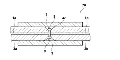
尚、図1において、膜体41はフェルール2aの端面91aに成膜される薄膜として説明したが、フェルール2aと2bを直接当接させることがないように保護媒体が配置されていればよく、例えば図2に示すような光デバイス70であってもよい。図2に示す光デバイス70は、スリーブ3の内部に保護媒体47が配置されている。具体的には、例えば、スリーブ3の一端と他端からフェルール2が挿入されても光ファイバ1aと1bとが直接当接されずに保護媒体47を介して当接されるように、保護媒体47を挟み込んだリング状のフランジ9をスリーブ3の内側に配置する。保護媒体47は、短波長領域の光に対する透過性が高い材質によって構成され、例えば、テフロン(登録商標)等が挙げられる。
In FIG. 1, the
〔実施例2〕
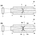
図3は、実施例2における光デバイス30の断面図を示した図である。光デバイス30のように、光導波路のないガラス等の透明部材6と光ファイバ1bを膜体43を介在させてスリーブ3に挿入して固定し、光学的に当接させてもよい。図3(a)に示すように、レンズ7に照射された光は透明部材6の端面92aに結合されて入射される。端面92aに結合された光は膜体43を介して光ファイバ1bの入射端から入射される。尚、膜体43は単層膜、多層膜の何れでもよく、材質、膜厚等は実施例1に記載したものと同様である。また、効果においても実施例1と同様の効果を奏する。また、図3(b)に示す光デバイス40ように、透明部材6の端面92aとフェルール2bの端面92bのそれぞれに膜体44a、44bが成膜されてもよい。
[Example 2]
FIG. 3 is a cross-sectional view of the
このように、ライトガイドに限らずガラス等からなる光学部材とライトガイドの光学的な当接部においても、前記膜体を介在して当接させることで実施例1と同様の効果を奏することができる。更に、レーザ光のように高密度の光を伝播するガラス等からなる光学部材同士を光学的に当接させる構成において、前記膜体を介在して結合させるようにしても良い。その場合、膜体43は単層膜、多層膜の何れでもよく、材質、膜厚等は実施例1に記載したものと同様である。
Thus, not only the light guide but also an optical member made of glass or the like and the optical contact portion of the light guide have the same effect as in the first embodiment by contacting the film body with the film body interposed therebetween. Can do. Furthermore, in a configuration in which optical members made of glass or the like that propagates high-density light such as laser light are optically abutted, the film bodies may be interposed. In that case, the
また、図4に示す光デバイス50のように、貫通孔に光ファイバ1cが挿入されたファイバスタブ8と光ファイバ1bを膜体45を介在させてスリーブ3に挿入して固定し、光学的に当接させてもよい。図4(a)に示すように、光デバイス50は、ファイバスタブ8と端面91bに膜体45が成膜されたフェルール2bがスリーブ3に挿入されて固定される。レンズ7に照射された光はファイバスタブ8に挿入された光ファイバ1cの入射端に結合されて入射され、光ファイバ1cの出射端から出射した光は膜体45を介して光ファイバ1bの入射端から入射される。尚、膜体45はファイバスタブ8側に成膜されていてもよい。また、図4(b)に示すように、ファイバスタブ8の端面93bとフェルール2bの端面91bのそれぞれに膜体46a、46bが成膜されてもよい。
Further, as in the
〔実施例3〕
図5は、実施例3における光デバイス70及び80の断面図の一例を示した図である。まず図5(a)に示す光デバイス70について説明する。同図のように、貫通孔に光ファイバ1aが挿入されたフェルール2aの端面91aに膜51、52の順に2層以上の多層膜を成膜させてもよい。
Example 3
FIG. 5 is a diagram illustrating an example of a cross-sectional view of the
このとき、膜52と貫通孔に光ファイバ1bが挿入されたフェルール2bの端面91bとの当接部における密着性より、膜51と膜52の密着性及び膜51と端面91aとの密着性の方が高いこととする。つまり、フェルール2a及び2bをスリーブ3に挿入して膜52とフェルール2bの端面91bとを当接させ、その後離間させたときに、膜52と端面91bとの密着性がいいと、離間させたときに膜52の端面91bと当接していた部分が剥離してしまい、膜52が損傷し、更に端面91bに膜52の一部が付着して、光デバイス70の再使用ができなくなってしまう。従って、膜52と端面91bとの当接部における密着性より、膜51と膜52の密着性及び膜51と端面91bとの密着性の方が高くなるような膜51及び52を用いることによって、離間時における膜52の剥離を防いで当接部における損傷をなくすことができ、安定した光デバイス70を提供することができる。
At this time, the adhesiveness between the
尚、本実施例では膜51及び52を積層させた2層膜について説明したが、2層以上の多層膜であってもよい。このとき、多層膜の最上層膜と端面91bとの当接部における密着性より、多層膜の最上層膜より下層の膜同士の密着性、及び多層膜の最下層膜と端面91aとの密着性の方が高いことが望ましい。
In this embodiment, the two-layer film in which the
また多層膜の最上層膜(図5における膜52)は、フッ化物であって、Siを含まないもの(例えば、YF3、LiF、MgF2、NaF、LaF3、BaF2、CaF2及びAlF3等の何れか)であることが望ましい。また、多層膜の最上層膜より下層の膜はSiを含まない酸化膜(例えば、MgO等)であることが望ましい。
Further, the uppermost layer film (
更に、図5(b)に示すように、多層膜を端面91a及び端面91bの双方に成膜させてもよい。この場合、膜52と膜61の密着性より、膜51と膜52の密着性及び膜51と端面91bとの密着性、膜61と膜62の密着性及び膜62と端面91bとの密着性の方が高いこととする。
Furthermore, as shown in FIG. 5B, a multilayer film may be formed on both the
また、端面91a、91bに成膜された各多層膜の膜厚は実施例1に記載した式(1)〜(3)を満足することが望ましい。 Further, it is desirable that the film thicknesses of the multilayer films formed on the end faces 91a and 91b satisfy the formulas (1) to (3) described in the first embodiment.
1a、1b、1c、90 光ファイバ
2a、3b フェルール
3 スリーブ
41〜46 膜体
47 保護媒体
1a, 1b, 1c, 90
Claims (18)
前記第1の光学部材の出射端と前記第2の光学部材の入射端の間に、前記第1の光学部材と前記第2の光学部材の接着を抑止する保護媒体が配置され、前記第1の光学部材の出射端と前記保護媒体、また該保護媒体と前記第2の光学部材の入射端とがそれぞれ当接して配置され、
前記保護媒体が、前記第1の光学部材の出射端に成膜された膜体及び前記第2の光学部材の入射端に成膜された膜体から成り、前記第1の光学部材の出射端及び前記第2の光学部材の入射端に成膜された前記膜体の互いに当接する面が互いに異なる物質によって構成されることを特徴とする光デバイス。 A first optical member that emits incident light from the exit end; and a second optical member that enters light emitted from the exit end of the first optical member from an entrance end opposite to the exit end. In the optical device
During the entrance end of the second optical member and the exit end of said first optical member, a protective medium for suppressing adhesion of the first optical member and the second optical member is disposed, the first The exit end of the optical member and the protective medium, and the protective medium and the incident end of the second optical member are disposed in contact with each other,
The protective medium includes a film body formed on the exit end of the first optical member and a film body formed on the entrance end of the second optical member, and the exit end of the first optical member. And an optical device in which surfaces of the film bodies formed on the incident end of the second optical member are in contact with each other .
前記第1の光学部材の出射端と前記第2の光学部材の入射端の間に、保護媒体が配置され、前記第1の光学部材の出射端と前記保護媒体、また該保護媒体と前記第2の光学部材の入射端とがそれぞれ当接して配置され、
前記保護媒体は、前記第1の光学部材と前記第2の光学部材とを500[g重]の荷重で該保護媒体と当接させ、後に離間させても、前記出射端と前記入射端を再使用可能な状態に維持する透明な保護媒体であり、
前記保護媒体が、前記第1の光学部材の出射端に成膜された膜体及び前記第2の光学部材の入射端に成膜された膜体から成り、前記第1の光学部材の出射端及び前記第2の光学部材の入射端に成膜された前記膜体の互いに当接する面が互いに異なる物質によって構成されることを特徴とする光デバイス。 A first optical member that emits incident light from the exit end; and a second optical member that enters light emitted from the exit end of the first optical member from an entrance end opposite to the exit end. In the optical device
A protective medium is disposed between the output end of the first optical member and the input end of the second optical member, and the output end of the first optical member and the protective medium, and the protective medium and the first optical member. And the incident ends of the two optical members are in contact with each other,
Even if the protective medium causes the first optical member and the second optical member to abut against the protective medium with a load of 500 g weight and is separated later, the emission end and the incident end are separated from each other. A transparent protective medium that keeps it reusable ,
The protective medium includes a film body formed on the exit end of the first optical member and a film body formed on the entrance end of the second optical member, and the exit end of the first optical member. And an optical device in which surfaces of the film bodies formed on the incident end of the second optical member are in contact with each other .
前記第1の光学部材の出射端に成膜された前記多層膜の最上層膜と前記第2の光学部材の入射端に成膜された前記多層膜の最上層膜とが、互いに異なる物質によって構成される膜体であり、
前記第1の光学部材の出射端に成膜された前記多層膜の最上層膜と前記第2の光学部材の入射端に成膜された前記多層膜の最上層膜との当接部における密着性より、前記各多層膜を構成する膜同士の密着性、及び前記各多層膜の最下層膜と前記各光学部材との密着性の方が高いことを特徴とする請求項1〜3の何れか一項に記載の光デバイス。 The film body is a multilayer film;
The uppermost layer film of the multilayer film formed on the emission end of the first optical member and the uppermost layer film of the multilayer film formed on the incident end of the second optical member are made of different materials. A film body composed of
Adherence at the contact portion between the uppermost layer film of the multilayer film formed at the exit end of the first optical member and the uppermost layer film of the multilayer film formed at the incident end of the second optical member from gender, any claim 1 to 3, wherein said adhesion between the films constituting each multi-layered film, and the possible direction of adhesion between the lowermost layer and the optical members is high in each multilayer film the optical device according to an item or.
Priority Applications (5)
| Application Number | Priority Date | Filing Date | Title |
|---|---|---|---|
| JP2006155613A JP4963375B2 (en) | 2005-11-02 | 2006-06-05 | Optical device, optical member and light guide |
| CN200610130898XA CN1982931B (en) | 2005-11-02 | 2006-11-01 | Optical device, optical member and optical pipe |
| TW095140343A TWI422884B (en) | 2005-11-02 | 2006-11-01 | Optical device having connections with optical members through protective medium |
| KR1020060108007A KR101258160B1 (en) | 2005-11-02 | 2006-11-02 | Optical device having connections with optical members through protective medium |
| US11/591,560 US7653275B2 (en) | 2005-11-02 | 2006-11-02 | Optical device having connections with optical members through protective medium |
Applications Claiming Priority (5)
| Application Number | Priority Date | Filing Date | Title |
|---|---|---|---|
| JP2005319226 | 2005-11-02 | ||
| JP2005319226 | 2005-11-02 | ||
| JP2006090100 | 2006-03-29 | ||
| JP2006090100 | 2006-03-29 | ||
| JP2006155613A JP4963375B2 (en) | 2005-11-02 | 2006-06-05 | Optical device, optical member and light guide |
Publications (2)
| Publication Number | Publication Date |
|---|---|
| JP2007293228A JP2007293228A (en) | 2007-11-08 |
| JP4963375B2 true JP4963375B2 (en) | 2012-06-27 |
Family
ID=38173578
Family Applications (1)
| Application Number | Title | Priority Date | Filing Date |
|---|---|---|---|
| JP2006155613A Active JP4963375B2 (en) | 2005-11-02 | 2006-06-05 | Optical device, optical member and light guide |
Country Status (5)
| Country | Link |
|---|---|
| US (1) | US7653275B2 (en) |
| JP (1) | JP4963375B2 (en) |
| KR (1) | KR101258160B1 (en) |
| CN (1) | CN1982931B (en) |
| TW (1) | TWI422884B (en) |
Families Citing this family (4)
| Publication number | Priority date | Publication date | Assignee | Title |
|---|---|---|---|---|
| WO2015150149A1 (en) * | 2014-03-31 | 2015-10-08 | Koninklijke Philips N.V. | Optical connector for sterile applications |
| TWM540290U (en) * | 2016-12-30 | 2017-04-21 | Luxnet Corp | Optical communication module for improving photo-coupling efficiency |
| CN111479534B (en) * | 2017-12-12 | 2023-02-17 | 爱尔康公司 | Thermally robust laser probe assembly |
| US20220075120A1 (en) * | 2019-01-08 | 2022-03-10 | Nippon Telegraph And Telephone Corporation | Optical fiber and manufacturing method thereof |
Family Cites Families (23)
| Publication number | Priority date | Publication date | Assignee | Title |
|---|---|---|---|---|
| JPS59218405A (en) * | 1983-05-27 | 1984-12-08 | Sumitomo Electric Ind Ltd | Fiber for transmission of light energy |
| US4738497A (en) * | 1984-10-05 | 1988-04-19 | Matsushita Electric Industrial Co., Ltd. | Antireflection film |
| US5157461A (en) * | 1990-06-14 | 1992-10-20 | Smiths Industries Aerospace & Defense Systems Inc. | Interface configuration for rate sensor apparatus |
| US5308656A (en) * | 1991-07-16 | 1994-05-03 | Adc Telecommunications, Inc. | Electroformed mask and use therefore |
| JPH05181040A (en) | 1991-12-28 | 1993-07-23 | Nec Corp | Optical connector and its production |
| GB9326429D0 (en) * | 1993-12-24 | 1994-02-23 | Bt & D Technologies Ltd | An optical device and method of making the same |
| CA2176594A1 (en) * | 1994-09-16 | 1996-03-21 | Seiji Fukuda | Wide band optical fiber, optical fiber core wire and optical fiber cord |
| JPH09221342A (en) | 1996-02-09 | 1997-08-26 | Nikon Corp | Method for joining optical members together and joined optical component thereby |
| JP3530951B2 (en) * | 1996-03-29 | 2004-05-24 | 株式会社日立コミュニケーションテクノロジー | Optical fiber, optical amplifier and optical transmission system |
| US6589650B1 (en) * | 2000-08-07 | 2003-07-08 | 3M Innovative Properties Company | Microscope cover slip materials |
| US6203208B1 (en) * | 1998-11-05 | 2001-03-20 | Illinois Tool Works Inc. | Fiber optic lighting system connector coupling medium |
| JP2000266939A (en) * | 1999-03-12 | 2000-09-29 | Japan Aviation Electronics Industry Ltd | Optical fiber connector |
| JP2001166179A (en) * | 1999-12-03 | 2001-06-22 | Sumitomo Electric Ind Ltd | Method and tool for assembling optical connector |
| US7036998B2 (en) * | 2001-05-17 | 2006-05-02 | Sumitomo Electric Industries, Ltd. | Optical part, optical module sleeve, optical receiving module, optical communication module, and method of making optical part |
| JP2003287655A (en) * | 2002-03-27 | 2003-10-10 | Ntt Afty Corp | Optical connector type wavelength filter |
| JP2003289655A (en) * | 2002-03-27 | 2003-10-10 | Honda Motor Co Ltd | Cage rotor |
| JP2004206068A (en) * | 2002-10-29 | 2004-07-22 | Kyocera Corp | Optical fiber and working method therefor |
| JP3929405B2 (en) * | 2003-01-06 | 2007-06-13 | 信越ポリマー株式会社 | Optical fiber connection device |
| JP2004252424A (en) * | 2003-01-31 | 2004-09-09 | Fuji Photo Film Co Ltd | Splicing structure of optical fiber |
| KR20040070092A (en) * | 2003-01-31 | 2004-08-06 | 후지 샤신 필름 가부시기가이샤 | Connection structure of optical fiber |
| JP2004279495A (en) | 2003-03-13 | 2004-10-07 | Nikon Corp | Beam splitter and optical measuring instrument |
| JP2005234025A (en) * | 2004-02-17 | 2005-09-02 | Omron Corp | Optical waveguide apparatus |
| US7141927B2 (en) * | 2005-01-07 | 2006-11-28 | Perkinelmer Optoelectronics | ARC lamp with integrated sapphire rod |
-
2006
- 2006-06-05 JP JP2006155613A patent/JP4963375B2/en active Active
- 2006-11-01 CN CN200610130898XA patent/CN1982931B/en active Active
- 2006-11-01 TW TW095140343A patent/TWI422884B/en active
- 2006-11-02 KR KR1020060108007A patent/KR101258160B1/en active IP Right Grant
- 2006-11-02 US US11/591,560 patent/US7653275B2/en active Active
Also Published As
| Publication number | Publication date |
|---|---|
| TWI422884B (en) | 2014-01-11 |
| KR20070047727A (en) | 2007-05-07 |
| CN1982931A (en) | 2007-06-20 |
| US7653275B2 (en) | 2010-01-26 |
| TW200732719A (en) | 2007-09-01 |
| CN1982931B (en) | 2011-06-22 |
| KR101258160B1 (en) | 2013-04-25 |
| JP2007293228A (en) | 2007-11-08 |
| US20070140617A1 (en) | 2007-06-21 |
Similar Documents
| Publication | Publication Date | Title |
|---|---|---|
| US11119271B2 (en) | Triple clad fiber | |
| JP4963375B2 (en) | Optical device, optical member and light guide | |
| JP2008275997A (en) | Light guide member | |
| JP5106905B2 (en) | Optical fiber end face protection structure | |
| WO2018062484A1 (en) | Optical connection structure and optical module | |
| JP2008256765A (en) | Fiber bundle and light source device | |
| JP2008275996A (en) | Light guide member | |
| KR101470892B1 (en) | Optical device and exposure apparatus | |
| JP2008250183A (en) | Optical device | |
| JP2008250184A (en) | Fiber light source apparatus | |
| JP5873022B2 (en) | Anti-reflection coating for adhesive protection | |
| EP3992672A1 (en) | Optical element, optical system, and optical apparatus | |
| JP2003084167A (en) | Collimator | |
| JP2010205926A (en) | Optical fiber device and method of manufacturing the same | |
| JPH0777601A (en) | Two-wavelength antireflection film | |
| JPH10177112A (en) | Optical fiber with filter and its production | |
| JP3073586B2 (en) | Optical fiber connector and optical module using the same | |
| JPH08310840A (en) | Reflection preventing film | |
| JP2018036361A (en) | Optical fiber bundle, combiner, laser device, and method of manufacturing optical fiber bundle | |
| JP6779070B2 (en) | Fiber optic bundles, combiners, and laser devices | |
| JP2005004022A (en) | Antireflection coating | |
| JPS60114801A (en) | Reflection preventing film | |
| JPH10260337A (en) | Optical fiber bundle and its manufacture | |
| Harrington | The development of hollow core waveguides for applications in telecommunications, sensors, and laser power delivery | |
| FR2828960A1 (en) | LASER SOURCE IN GUIDED OPTICS |
Legal Events
| Date | Code | Title | Description |
|---|---|---|---|
| A621 | Written request for application examination |
Free format text: JAPANESE INTERMEDIATE CODE: A621 Effective date: 20090217 |
|
| A977 | Report on retrieval |
Free format text: JAPANESE INTERMEDIATE CODE: A971007 Effective date: 20100930 |
|
| A131 | Notification of reasons for refusal |
Free format text: JAPANESE INTERMEDIATE CODE: A131 Effective date: 20111025 |
|
| A521 | Request for written amendment filed |
Free format text: JAPANESE INTERMEDIATE CODE: A523 Effective date: 20111222 |
|
| TRDD | Decision of grant or rejection written | ||
| A01 | Written decision to grant a patent or to grant a registration (utility model) |
Free format text: JAPANESE INTERMEDIATE CODE: A01 Effective date: 20120321 |
|
| A01 | Written decision to grant a patent or to grant a registration (utility model) |
Free format text: JAPANESE INTERMEDIATE CODE: A01 |
|
| A61 | First payment of annual fees (during grant procedure) |
Free format text: JAPANESE INTERMEDIATE CODE: A61 Effective date: 20120323 |
|
| R150 | Certificate of patent or registration of utility model |
Ref document number: 4963375 Country of ref document: JP Free format text: JAPANESE INTERMEDIATE CODE: R150 Free format text: JAPANESE INTERMEDIATE CODE: R150 |
|
| FPAY | Renewal fee payment (event date is renewal date of database) |
Free format text: PAYMENT UNTIL: 20150406 Year of fee payment: 3 |
|
| S111 | Request for change of ownership or part of ownership |
Free format text: JAPANESE INTERMEDIATE CODE: R313113 |
|
| R350 | Written notification of registration of transfer |
Free format text: JAPANESE INTERMEDIATE CODE: R350 |
|
| R250 | Receipt of annual fees |
Free format text: JAPANESE INTERMEDIATE CODE: R250 |
|
| R250 | Receipt of annual fees |
Free format text: JAPANESE INTERMEDIATE CODE: R250 |
|
| R250 | Receipt of annual fees |
Free format text: JAPANESE INTERMEDIATE CODE: R250 |
|
| R250 | Receipt of annual fees |
Free format text: JAPANESE INTERMEDIATE CODE: R250 |
|
| R250 | Receipt of annual fees |
Free format text: JAPANESE INTERMEDIATE CODE: R250 |
|
| R250 | Receipt of annual fees |
Free format text: JAPANESE INTERMEDIATE CODE: R250 |
|
| R250 | Receipt of annual fees |
Free format text: JAPANESE INTERMEDIATE CODE: R250 |
|
| R250 | Receipt of annual fees |
Free format text: JAPANESE INTERMEDIATE CODE: R250 |
|
| R250 | Receipt of annual fees |
Free format text: JAPANESE INTERMEDIATE CODE: R250 |
|
| R250 | Receipt of annual fees |
Free format text: JAPANESE INTERMEDIATE CODE: R250 |