JP4963159B2 - Piezoelectric / electrostrictive device - Google Patents
Piezoelectric / electrostrictive device Download PDFInfo
- Publication number
- JP4963159B2 JP4963159B2 JP2004335751A JP2004335751A JP4963159B2 JP 4963159 B2 JP4963159 B2 JP 4963159B2 JP 2004335751 A JP2004335751 A JP 2004335751A JP 2004335751 A JP2004335751 A JP 2004335751A JP 4963159 B2 JP4963159 B2 JP 4963159B2
- Authority
- JP
- Japan
- Prior art keywords
- piezoelectric
- thin diaphragm
- electrostrictive
- diaphragm portion
- plane
- Prior art date
- Legal status (The legal status is an assumption and is not a legal conclusion. Google has not performed a legal analysis and makes no representation as to the accuracy of the status listed.)
- Expired - Fee Related
Links
Images


Classifications
-
- H—ELECTRICITY
- H10—SEMICONDUCTOR DEVICES; ELECTRIC SOLID-STATE DEVICES NOT OTHERWISE PROVIDED FOR
- H10N—ELECTRIC SOLID-STATE DEVICES NOT OTHERWISE PROVIDED FOR
- H10N30/00—Piezoelectric or electrostrictive devices
- H10N30/20—Piezoelectric or electrostrictive devices with electrical input and mechanical output, e.g. functioning as actuators or vibrators
- H10N30/204—Piezoelectric or electrostrictive devices with electrical input and mechanical output, e.g. functioning as actuators or vibrators using bending displacement, e.g. unimorph, bimorph or multimorph cantilever or membrane benders
- H10N30/2047—Membrane type
- H10N30/2048—Membrane type having non-planar shape
-
- H—ELECTRICITY
- H10—SEMICONDUCTOR DEVICES; ELECTRIC SOLID-STATE DEVICES NOT OTHERWISE PROVIDED FOR
- H10N—ELECTRIC SOLID-STATE DEVICES NOT OTHERWISE PROVIDED FOR
- H10N30/00—Piezoelectric or electrostrictive devices
- H10N30/80—Constructional details
- H10N30/85—Piezoelectric or electrostrictive active materials
- H10N30/853—Ceramic compositions
Description
本発明は、圧電/電歪デバイスに関する。さらに詳しくは、屈曲変位を利用したアクチュエータや、流体特性、音圧、微小重量、加速度等を検出するための各種センサ(例えば、マイクロホン用センサ、粘度センサ等)として用いられる圧電/電歪デバイスに関する。 The present invention relates to a piezoelectric / electrostrictive device. More specifically, the present invention relates to an actuator using bending displacement and a piezoelectric / electrostrictive device used as various sensors (for example, a sensor for a microphone, a viscosity sensor, etc.) for detecting fluid characteristics, sound pressure, minute weight, acceleration, and the like. .
圧電/電歪デバイスは、アクチュエータや各種センサとして用いられている。このような圧電/電歪デバイスとしては、例えば、流体の密度、濃度、粘度等の特性の測定に利用されたものが開示されている(特許文献1参照)。このような圧電/電歪デバイスは、圧電/電歪デバイスの振動子としての振幅と、圧電/電歪デバイス(振動子)に接触する流体の粘性抵抗とに相関があることを利用してセンサとして用いられるものである。 Piezoelectric / electrostrictive devices are used as actuators and various sensors. As such a piezoelectric / electrostrictive device, for example, a device used for measuring characteristics such as density, concentration, viscosity and the like of a fluid is disclosed (see Patent Document 1). Such a piezoelectric / electrostrictive device utilizes a correlation between the amplitude of a piezoelectric / electrostrictive device as a vibrator and the viscous resistance of a fluid in contact with the piezoelectric / electrostrictive device (vibrator). It is used as
一般に、振動子の振動のような機械系での振動形態は、電気系での等価回路に置き換えることができ、流体中で圧電/電歪デバイス(振動子)を振動させ、この振動子が流体の粘性抵抗に基づいて機械的抵抗を受けることによって振動子を構成する圧電/電歪素子の等価回路の電気的定数が変化するのを利用して、流体の粘度、密度、濃度等の特性を測定している。ここで、測定可能な流体としては、液体及び気体を挙げることができる。このような液体としては、水、アルコール、油等の単一の成分からなるものであってもよく、これらに可溶又は不溶な媒質を、溶解、混合又は懸濁せしめたもの、スラリー、ペースト等であってもよい。 In general, a vibration form in a mechanical system such as vibration of a vibrator can be replaced with an equivalent circuit in an electric system, and a piezoelectric / electrostrictive device (vibrator) is vibrated in a fluid. By utilizing the fact that the electrical constant of the equivalent circuit of the piezoelectric / electrostrictive element constituting the vibrator changes due to the mechanical resistance based on the viscous resistance of the fluid, characteristics such as the viscosity, density, and concentration of the fluid Measuring. Here, examples of the measurable fluid include liquid and gas. Such a liquid may be composed of a single component such as water, alcohol, oil, and the like, a slurry, a paste in which a soluble or insoluble medium is dissolved, mixed or suspended. Etc.
また、検出する電気的定数としては、例えば、損失係数、位相、抵抗、リアクタンス、コンダクダンス、サセプタンス、インダクタンス、キャパシタンス等を挙げることができ、特に、等価回路の共振周波数近傍で極大又は極小変化点を1つ有する損失係数又は位相が好ましく用いられる。これにより流体の粘度だけではなく、密度や濃度(例えば、硫酸水溶液中の硫酸濃度)をも測定することができる。なお、振動形態の変化を検出する指標として、電気的定数以外に、測定精度、耐久性の観点から特に問題がなければ、共振周波数の変化を利用することもできる。また、圧電/電歪素子として強誘電体を用いた場合には、パルス状の電界を与えた後に、強誘電体の双極子モーメントの遅れに起因して発生する電荷を電圧として検知し、これの変化を利用することもできる。 In addition, examples of the electrical constant to be detected include loss factor, phase, resistance, reactance, conductance, susceptance, inductance, capacitance, and the like. Particularly, the maximum or minimum change point in the vicinity of the resonance frequency of the equivalent circuit. A loss factor or phase having one is preferably used. Thereby, not only the viscosity of the fluid but also the density and concentration (for example, sulfuric acid concentration in sulfuric acid aqueous solution) can be measured. As an index for detecting a change in vibration form, a change in resonance frequency can be used as long as there is no particular problem from the viewpoint of measurement accuracy and durability, in addition to an electrical constant. In addition, when a ferroelectric is used as the piezoelectric / electrostrictive element, a charge generated due to a delay in the dipole moment of the ferroelectric is detected as a voltage after applying a pulsed electric field. You can also take advantage of these changes.
このような圧電/電歪デバイスとして、厚肉部、及び厚肉部と一体的に形成されて空洞を形成する薄肉ダイヤフラム部を有するセラミック基体と、その外表面に固定された圧電/電歪素子とを備え、圧電/電歪素子を構成する下部電極とは独立した位置に、補助電極を形成し、その補助電極の一部が圧電/電歪膜の下側の一部に入り込ませるように形成されたものが開示されている(特許文献2参照)。このように構成することによって、上部電極を補助電極及び圧電/電歪素子の面上で断線することなく連続して形成することが可能となり、上部電極の接続の信頼性を向上させることができる。なお、被測定流体は、貫通孔を経由して空洞内に導入、充填される。さらに、補助電極を、薄肉ダイヤフラム部の外表面上だけでなく、厚肉部にまで連続して形成することにより、安定したデバイス特性と、使用条件による制限を受け難い圧電/電歪デバイスを得ることができる。
しかしながら、上述の特許文献に開示された圧電/電歪デバイス等においては、圧電/電歪素子の駆動に連動して薄肉ダイヤフラム部だけを振動させようとするものであるが、実際は、薄肉ダイヤフラム部だけではなく、厚肉部をも振動させることになり、薄肉ダイヤフラム部の振動エネルギーが減衰して、変位(振幅)を減少させるとともに応答性を低下させてしまうことになり、高精度(高分解能、高感度)な検知が困難となるという問題があった。 However, in the piezoelectric / electrostrictive device disclosed in the above-mentioned patent document, only the thin diaphragm portion is caused to vibrate in conjunction with the driving of the piezoelectric / electrostrictive element. In addition to oscillating the thick-walled part, the vibration energy of the thin-walled diaphragm part is attenuated, reducing the displacement (amplitude) and lowering the responsiveness with high accuracy (high resolution) , High sensitivity) is difficult to detect.
本発明は、上述の問題に鑑みてなされたものであり、薄肉ダイヤフラム部の振動の減衰が有効に防止され、変位(振幅)を高く維持するとともに応答性に優れ、高精度(高分解能、高感度)な検知が可能な圧電/電歪デバイスを提供することを目的とする。 The present invention has been made in view of the above-described problems, and is capable of effectively preventing the vibration of the thin diaphragm portion from being attenuated, maintaining high displacement (amplitude) and excellent response, and high accuracy (high resolution, high resolution). It is an object to provide a piezoelectric / electrostrictive device capable of sensitive detection.
上記目的を達成するため、本発明によれば以下の圧電/電歪デバイスが提供される。 In order to achieve the above object, the present invention provides the following piezoelectric / electrostrictive device.
[1]厚肉部と、前記厚肉部の端面上に一体的に架設された薄肉ダイヤフラム部、及び、前記厚肉部及び前記薄肉ダイヤフラム部によって外部に連通するように形成された空洞とからなるセラミック基体、及び前記セラミック基体の薄肉ダイヤフラム部の外表面上に固定された層構造からなる下部電極、圧電/電歪膜及び上部電極を含む圧電/電歪素子とから構成され、前記セラミック基体の薄肉ダイヤフラム部が、前記圧電/電歪素子の駆動に連動して振動することが可能であり、下記(A)〜(D)に規定された形状及び寸法関係を満たすことを特徴とする圧電/電歪デバイス。
(A)前記薄肉ダイヤフラム部の形状が、外方に凸のアーチ形状であり、かつ前記アーチ形状の外方への突出量が、5〜50μmである
(B)前記薄肉ダイヤフラム部の架設幅が、600〜2000μmである
(C)前記厚肉部の高さの、その幅に対する割合(高さ/幅)が、0.25〜3である
(D)前記薄肉ダイヤフラム部の外形形状は、アスペクト比が1.5以上の、長方形、長円形、又は楕円形である
[1] From a thick part, a thin diaphragm part integrally constructed on an end surface of the thick part, and a cavity formed to communicate with the outside by the thick part and the thin diaphragm part And a piezoelectric / electrostrictive element including a lower electrode having a layer structure fixed on an outer surface of a thin diaphragm portion of the ceramic substrate, a piezoelectric / electrostrictive film, and an upper electrode. The thin-walled diaphragm portion can vibrate in conjunction with the driving of the piezoelectric / electrostrictive element, and satisfies the shape and dimensional relationship defined in (A) to (D) below. / Electrostrictive device.
(A) the shape of the thin diaphragm portion is a outward protruding arch shape, and amount of projection of the outside of the arch-shaped, Ru 5~50μm der (B) mounting width of the thin diaphragm portion but
(D) The outer shape of the thin diaphragm portion is a rectangle, an oval, or an ellipse with an aspect ratio of 1.5 or more.
[2]前記薄肉ダイヤフラム部及び薄肉ダイヤフラム部の外表面上に固定された圧電/電歪素子をそれぞれ2以上有し、前記薄肉ダイヤフラム部及び前記圧電/電歪素子が、第1の平面上及び/又は前記第1の平面に平行な第2の平面上にそれぞれ配設されてなる前記[1]に記載の圧電/電歪デバイス。 [2] There are two or more piezoelectric / electrostrictive elements each fixed on the outer surface of the thin diaphragm part and the thin diaphragm part, and the thin diaphragm part and the piezoelectric / electrostrictive element are on the first plane and // The piezoelectric / electrostrictive device according to [1], wherein the piezoelectric / electrostrictive device is disposed on a second plane parallel to the first plane.
[3]前記薄肉ダイヤフラム部及び薄肉ダイヤフラム部の外表面上に固定された圧電/電歪素子をそれぞれ2以上有し、前記薄肉ダイヤフラム部及び前記圧電/電歪素子が、第1の平面上、前記第1の平面に平行な第2の平面上及び/又は前記第1の平面に垂直な第3の平面上にそれぞれ配設されてなる前記[1]に記載の圧電/電歪デバイス。 [3] There are two or more piezoelectric / electrostrictive elements each fixed on the outer surface of the thin diaphragm part and the thin diaphragm part, and the thin diaphragm part and the piezoelectric / electrostrictive element are on the first plane, The piezoelectric / electrostrictive device according to [1], wherein the piezoelectric / electrostrictive device is disposed on a second plane parallel to the first plane and / or on a third plane perpendicular to the first plane.
[4]前記圧電/電歪素子が、膜形成手法にて形成されたものであるとともに、前記圧電/電歪素子の構成材料が、前記薄肉ダイヤフラム部の外表面上に配設された後、熱処理されて、前記薄肉ダイヤフラム部の外表面上に固定されることによって得られたものである前記[1]〜[3]のいずれかに記載の圧電/電歪デバイス。 [4] The piezoelectric / electrostrictive element is formed by a film forming method, and the constituent material of the piezoelectric / electrostrictive element is disposed on the outer surface of the thin diaphragm portion; The piezoelectric / electrostrictive device according to any one of [1] to [3], wherein the piezoelectric / electrostrictive device is obtained by being heat-treated and fixed on the outer surface of the thin-walled diaphragm portion.
本発明によって、薄肉ダイヤフラム部の振動の減衰が有効に防止され、変位(振幅)を高く維持するとともに応答性に優れ、高精度(高分解能、高感度)な検知が可能な圧電/電歪デバイスが提供される。 According to the present invention, a piezoelectric / electrostrictive device capable of effectively preventing vibration attenuation of a thin diaphragm portion, maintaining a high displacement (amplitude), having excellent responsiveness, and detecting with high precision (high resolution, high sensitivity). Is provided.
以下、本発明の圧電/電歪デバイスを実施するための最良の形態について、図面を参照しつつ説明する。 Hereinafter, the best mode for carrying out the piezoelectric / electrostrictive device of the present invention will be described with reference to the drawings.
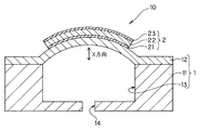
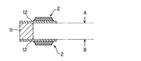
図1は、本発明の圧電/電歪デバイスの一の実施の形態を模式的に示す説明図であり、図2は、図1に示す圧電/電歪デバイスの一の実施の形態における形状及び寸法関係を模式的に示す説明図である。 FIG. 1 is an explanatory view schematically showing one embodiment of the piezoelectric / electrostrictive device of the present invention, and FIG. 2 shows the shape and shape in one embodiment of the piezoelectric / electrostrictive device shown in FIG. It is explanatory drawing which shows a dimensional relationship typically.
図1、2に示すように、本実施の形態の圧電/電歪デバイスは、厚肉部11、及び厚肉部11の端面上に一体的に架設された薄肉ダイヤフラム部12を有し、厚肉部11及び薄肉ダイヤフラム部12によって外部に連通する空洞13が形成されたセラミック基体1と、セラミック基体1の薄肉ダイヤフラム部12の外表面上に固定された、下部電極21、圧電/電歪膜22及び上部電極23を含む層構造を有する圧電/電歪素子2とを備え、圧電/電歪素子2の駆動に連動してセラミック基体1の薄肉ダイヤフラム部12が振動することが可能な圧電/電歪デバイス10であって、下記(A)〜(C)に規定された形状及び寸法関係を満たすことを特徴とするものである。
(A)薄肉ダイヤフラム部12の形状が、外方に凸のアーチ形状であり、かつアーチ形状の外方への突出量(h)が、5〜50μmであること、
(B)薄肉ダイヤフラム部の架設幅(m)が、600〜2000μmであること、
(C)前記厚肉部の高さの、その幅に対する割合(高さ/幅)が、0.25〜3であること。
As shown in FIGS. 1 and 2, the piezoelectric / electrostrictive device of the present embodiment includes a
(A) The shape of the
(B) The erection width (m) of the thin diaphragm portion is 600 to 2000 μm,
(C) The ratio (height / width) of the thickness of the thick part to its width is 0.25-3.
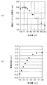
本実施の形態においては、上述のように、(A)薄肉ダイヤフラム部12の形状が、外方に凸のアーチ形状であり、かつアーチ形状の外方への突出量(h)が、5〜50μmであることが必要であり、5〜30μmであることが好ましい。外方に凸のアーチ形状とすることによって、圧電/電歪素子2に発生する歪みや応力を効率よく変位に変えることが可能となる。すなわち、外方に凸のアーチ形状の薄肉ダイヤフラム部12の外表面に形成された圧電/電歪素子2は、駆動されることによって薄肉ダイヤフラム部12の外表面に垂直な方向(X方向)に変位するから、圧電/電歪素子2の駆動に連動してセラミック基体1の薄肉ダイヤフラム部12も空洞13の内容積を変化させつつ、その外表面に垂直な方向(X方向)に振動することになるのであるが、薄肉ダイヤフラム部12の外方に凸のアーチ形状の外表面に対して、圧電/電歪素子2(具体的には、少なくとも下部電極21及び圧電/電歪膜22)が形成されることによって、薄肉ダイヤフラム部12の圧電/電歪素子2が形成される部位の剛性を有効に向上させることが可能となる。また、薄肉ダイヤフラム部12が、外方に凸のアーチ形状を有することによって、薄肉ダイヤフラム部12の外表面側からの押圧力に対する機械的強度を向上させることが可能となる。さらに、圧電/電歪素子2が形成された薄肉ダイヤフラム部12の固有振動数及び応答速度を増大させることも可能となる。また、アーチ形状の外方への突出量(h)が、5〜50μmの範囲を外れると、図3(a)、(b)に示すように、強く鮮明な信号を出力するために必要な、十分に大きな変位、及び減衰しにくい振動モードを確保することが困難となる。なお、突出量(h)が大きくなるにつれて、変位が小さくなるとともに、不要な変形が起こりやすくなるため、出力信号のS/N比が小さくなるが、突出量(h)が5〜30μmの範囲内であると、確実に鮮明な出力信号を得ることができるため好ましい。すなわち、図3(a)は、薄肉ダイヤフラム部の突出量(h)と薄肉ダイヤフラム部の変位との関係を示すグラフであり、突出量(h)が、5〜50μmの範囲を外れると変位が急激に小さくなることを示している。図3(b)は、薄肉ダイヤフラム部の突出量(h)と厚肉部の開きとの関係を示すグラフであり、突出量(h)が5μm未満であると、厚肉部が空洞側に倒れこみ、50μmを超えると、薄肉ダイヤフラム部の剛性が低下し、薄肉ダイヤフラム部の中央が変形の腹になる(例えば、振動の場合は1次モードになる)ような所望の変形にならない(突出量(h)が50μmを超えると厚肉部の開きが変化しないことが、これを示している)。なお、「厚肉部の開き」とは、図2に示す基準点Tが厚肉部11の幅(q)方向に移動する量を意味し、幅(q)方向で外方に向かって(図では右側に)移動する場合は正の量、幅(q)方向で内方に向かって(図では左側に)移動する場合は負の量を示す。
In the present embodiment, as described above, (A) the shape of the
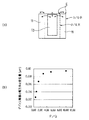
また、(B)薄肉ダイヤフラム部の架設幅(m)が、600〜2000μmであることが必要であり、600〜1500μmであることが好ましい。ここで、薄肉ダイヤフラム部の架設幅(m)とは、空洞13の短手方向の長さを意味し、例えば、空洞13の形状(X方向に垂直な断面形状)が円形である場合においては、その直径、長方形である場合においては、その短辺長さ、楕円形である場合においては、その短軸長さ等に相当する長さを意味する。図4(a)、(b)に示すように、薄肉ダイヤフラム部の架設幅(m)が600μm未満であると、流路抵抗が増大するとともに変位が小さくなってしまい、2000μmを超えると、薄肉ダイヤフラム部の剛性が低くなり固有振動数が低下するとともに減衰しやすくなるため十分な出力信号が得られない。なお、架設幅(m)が1500μmを超えると、不要な変形が起こりやすくなるため、出力信号のS/N比が小さくなることがあるが(架設幅(m)が2000μmまでは不要な変形が起こりやすくはなるが許容範囲である)、架設幅(m)が600〜1500μmの範囲内であると、確実に鮮明な出力信号を得ることができるため好ましい。すなわち、図4(a)は、薄肉ダイヤフラム部の架設幅(m)と薄肉ダイヤフラム部の変位との関係を示すグラフであり、架設幅(m)が、600μm未満であると、変位が小さくなり十分な出力信号が得られないことを示している。図4(b)は、薄肉ダイヤフラム部の架設幅(m)と減衰の関係を示すグラフであり、架設幅(m)が、2000μmを超えると、薄肉ダイヤフラム部の剛性低下により固有振動数が低下し、また、不要な振動モードの影響を受けやすくなるため、減衰し易くなって十分な出力信号が得られないことを示している。また、架設幅(m)が600μm未満になると薄肉ダイヤフラム部の質量が小さくなり両端部における拘束の影響を受け易くなることから減衰し易くなって十分な出力信号が得られないことを示している。なお、図4(a)のグラフにおいては、薄肉ダイヤフラム部の突出量(h)が50μmの場合を○、20μmの場合を□、0μmの場合を△の点でそれぞれ示す。また、図4(b)の縦軸における減衰の具体的な尺度は、振動波振幅の比の値=[(第10振動波振幅/第5振動波振幅)×100(%)]で示した。ここで、第5振動波振幅とは、自由振動により生じた振幅の5番目のものを意味し、また、第10振動波振幅とは、自由振動により生じた振幅の10番目のものを意味する。第5振動波振幅をV5、第10振動波振幅をV10でそれぞれ表すと、振動波振幅の比の値は、[(V10/V5)×100(%)]で示されることになる。
Further, (B) the erected width (m) of the thin diaphragm portion needs to be 600 to 2000 μm, and preferably 600 to 1500 μm. Here, the installation width (m) of the thin diaphragm portion means the length of the
また、(C)厚肉部の高さ(p)の、その幅(q)に対する割合(高さ(p)/幅(q))が0.25〜3であることが必要であり、0.25〜1.5であることが好ましい。図5(a)、(b)及び図6(a)、(b)に示すように、この割合が0.25未満であると、薄肉ダイヤフラム部の駆動によるデバイス端部EのX方向振動が励起されやすくなり、薄肉ダイヤフラム部振動の減衰を引き起こす。また、割合が3を超えるように大きいと、薄肉ダイヤフラム部の駆動の際に、デバイス端部Eの幅方向振動が励起され易くなり薄肉ダイヤフラム部振動の減衰を引き起こす。なお、割合(高さ(p)/幅(q))が1.5を超えると、厚肉部の高次変形が発生しやすくなり、出力信号のS/N比が小さくなることがあるが、割合(高さ(p)/幅(q))が0.25〜1.5の範囲内であると、確実に鮮明な出力信号を得ることができるため好ましい。すなわち、図5(a)は、厚肉部の高さ(p)の、その幅(q)に対する割合(高さ(p)/幅(q))が小さいときに(図では実線で示す)、デバイス端部EのX方向振動は大きく励起される(割合が大きいときには(図では破線で示す)、デバイス端部EのX方向振動は小さく励起される)ことを模式的に示す説明図であり、また、図5(b)は、高さ(p)/幅(q)とデバイス端部EのX方向(図1参照)の変位量との関係を示すグラフであり、高さ(p)/幅(q)が0.25未満であると、デバイス端部EのX方向振動が励起され、薄肉ダイヤフラム部振動の減衰を引き起こすことを示している。図6(a)は、高さ(p)/幅(q)が3を超えるように大きいと(図では破線で示す)、デバイス端部Eの幅方向振動は大きく励起される(割合が小さいときには(図では実線で示す)、デバイス端部Eの幅方向振動は小さく励起される)ことを模式的に示す説明図であり、また、図6(b)は、高さ(p)/幅(q)とデバイス端部Eの幅方向の変位量との関係を示すグラフであり、高さ(p)/幅(q)が3を超えると、厚肉部が変形してしまい、薄肉ダイヤフラム部振動の減衰を引き起こすことを示している。 Further, it is necessary that the ratio (height (p) / width (q)) of the height (p) of the thick part (C) to the width (q) is 0.25 to 3, and 0 It is preferably 25 to 1.5. As shown in FIGS. 5A and 5B and FIGS. 6A and 6B, when this ratio is less than 0.25, the vibration in the X direction of the device end E due to the driving of the thin diaphragm portion is caused. It becomes easy to be excited and causes the vibration of the thin diaphragm part to be attenuated. On the other hand, if the ratio is large so as to exceed 3, the vibration in the width direction of the device end E is likely to be excited when the thin diaphragm portion is driven, and the thin diaphragm portion vibration is attenuated. If the ratio (height (p) / width (q)) exceeds 1.5, higher-order deformation of the thick-walled portion is likely to occur, and the S / N ratio of the output signal may be reduced. When the ratio (height (p) / width (q)) is in the range of 0.25 to 1.5, it is preferable because a clear output signal can be obtained with certainty. That is, FIG. 5A shows a case where the ratio (height (p) / width (q)) of the height (p) of the thick portion to the width (q) is small (shown by a solid line in the figure). The X direction vibration of the device end E is excited greatly (when the ratio is large (indicated by a broken line in the figure), the X direction vibration of the device end E is excited small). FIG. 5B is a graph showing the relationship between the height (p) / width (q) and the amount of displacement of the device end E in the X direction (see FIG. 1). ) / Width (q) of less than 0.25 indicates that the X-direction vibration of the device end E is excited and causes attenuation of the vibration of the thin diaphragm portion. 6A, when the height (p) / width (q) is large so as to exceed 3 (indicated by a broken line in the figure), the vibration in the width direction of the device end E is greatly excited (the ratio is small). FIG. 6B is an explanatory view schematically showing that sometimes (indicated by a solid line in the figure, the vibration in the width direction of the device end E is excited to be small), and FIG. 6B shows the height (p) / width It is a graph which shows the relationship between (q) and the displacement amount of the width direction of the device edge part E, and when a height (p) / width (q) exceeds 3, a thick part will deform | transform and a thin-walled diaphragm It is shown that this causes damping of the part vibration.
上述の構成を有することから、本実施の形態の圧電/電歪デバイスは、薄肉ダイヤフラム部の振動の減衰が有効に防止され、変位(振幅)を高く維持するとともに応答性に優れ、高精度(高分解能、高感度)な検知が可能なものとなる。 Since the piezoelectric / electrostrictive device of the present embodiment has the above-described configuration, the vibration of the thin diaphragm portion is effectively prevented from being attenuated, the displacement (amplitude) is maintained high and the response is excellent, and the high precision ( High resolution and high sensitivity) can be detected.
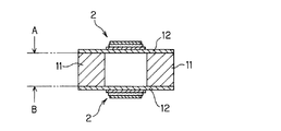
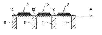
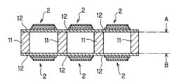
図1、2に示す実施の形態においては、2つの厚肉部11の端面上(第1の平面A上)に一体的に架設された薄肉ダイヤフラム部12及び薄肉ダイヤフラム部12の外表面上に固定された圧電/電歪素子2がそれぞれ1つ配設される場合について説明したが、図7〜10に示すように、他の実施の形態として、薄肉ダイヤフラム部12及び圧電/電歪素子2が、第1の平面A上及び/又は第1の平面Aに平行な第2の平面B上にそれぞれ配設されてなるものであってもよい。図7は、薄肉ダイヤフラム部12及び圧電/電歪素子2が、2つの厚肉部11のそれぞれの両端面上(第1の平面A上及び第1の平面Aに平行な第2の平面B上)にそれぞれ1つ配設された場合を示す。図8は、薄肉ダイヤフラム部12及び圧電/電歪素子2が、1つの厚肉部11の両端面上(第1の平面A上及び第1の平面Aに平行な第2の平面B上)にそれぞれ1つ、片持ち梁の状態で配設された場合を示す。図9は、薄肉ダイヤフラム部12及び圧電/電歪素子2が、4つの厚肉部11のそれぞれの片方の端面上(第1の平面A上)にそれぞれ3つ配設された場合を示す。図10は、薄肉ダイヤフラム部12及び圧電/電歪素子2が、4つの厚肉部11のそれぞれの両端面上(第1の平面A上及び第1の平面Aに平行な第2の平面B上)にそれぞれ3つ、合計6つ配設された場合を示す。
In the embodiment shown in FIGS. 1 and 2, the
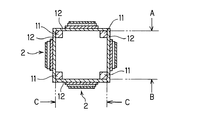
また、図11に示すように、他の実施の形態として、薄肉ダイヤフラム部12及び薄肉ダイヤフラム部12の外表面上に固定された圧電/電歪素子2をそれぞれ2以上有する場合、前記薄肉ダイヤフラム部及び前記圧電/電歪素子が、第1の平面A上、第1の平面Aに平行な第2の平面B上及び/又は第1の平面Aに垂直な第3の平面C上にそれぞれ配設されてなるものであってもよい。図11は、薄肉ダイヤフラム部12及び圧電/電歪素子2が、4つの厚肉部11のそれぞれ互いに平行な両端面及び互いに垂直な両端面上(第1の平面A上、第1の平面Aに平行な第2の平面B上及び第1の平面Aに垂直な第3の平面C(平面Cは二面ある)上)にそれぞれ1つ、合計4つ配設された場合を示す。
In addition, as shown in FIG. 11, as another embodiment, when there are two or more piezoelectric /
なお、図3〜6に示したグラフは、図7〜11に示すような薄肉ダイヤフラム部を2つ以上有する構成の圧電/電歪デバイスの場合、薄肉ダイヤフラム部12を互いに独立振動させることによって得た値をベースに作成されたものである。なお、これらのグラフは一例を示すものであり、薄肉ダイヤフラム部の厚さ14μm、突出量20μm、架設幅1500μm、厚肉部の高さ800μm、厚肉部の幅800μmの寸法関係を有するとともに、図7に示すような、対称に配置された2つの薄肉ダイヤフラム部を有するデバイスに基づいて作成されたグラフである。
The graphs shown in FIGS. 3 to 6 are obtained by causing the
本実施の形態においては、圧電/電歪素子2が、膜形成手法にて形成されたものであるとともに、圧電/電歪素子2の構成材料が、薄肉ダイヤフラム部12の外表面上に配設された後、熱処理されて、薄肉ダイヤフラム部12の外表面上に固定されることによって得られたものである場合に、各層間の接合性を向上させることが可能となり、その効果を最も有効に発揮することができる。
In the present embodiment, the piezoelectric /
以下、本発明の圧電/電歪デバイスに用いられる各構成要素について具体的に説明する。 Hereafter, each component used for the piezoelectric / electrostrictive device of this invention is demonstrated concretely.
本発明に用いられるセラミック基体1は、その材質が、耐熱性、化学的安定性、絶縁性を有するものであることが好ましい。これは、その外表面上に、後述する圧電/電歪素子2(下部電極21、圧電/電歪膜22、上部電極23を含む)を固定する際に、上述のように熱処理をすることがあるからであり、また、圧電/電歪デバイスが、センサ素子として、液体の特性のセンシングに用いられる場合、その液体が導電性や、腐食性を有することがあるからである。
The material of the ceramic substrate 1 used in the present invention is preferably one having heat resistance, chemical stability, and insulation. This is because heat treatment is performed as described above when fixing the piezoelectric / electrostrictive element 2 (including the
このような観点から、セラミック基体1の構成材料として好ましく用いられるセラミックとしては、例えば、安定化された酸化ジルコニウム、酸化アルミニウム、酸化マグネシウム、ムライト、窒化アルミニウム、窒化珪素、ガラス等を挙げることができる。中でも、安定化された酸化ジルコニウムが、薄肉ダイヤフラム部12を薄く構成した場合であっても機械的強度を高く保持することができること、及び靭性に優れること等から、さらに好ましい。
From such a viewpoint, examples of the ceramic preferably used as the constituent material of the ceramic substrate 1 include stabilized zirconium oxide, aluminum oxide, magnesium oxide, mullite, aluminum nitride, silicon nitride, and glass. . Among these, stabilized zirconium oxide is more preferable because it can maintain high mechanical strength even when the thin-
セラミック基体1の薄肉ダイヤフラム部12の厚さは、圧電/電歪素子2の駆動を制約することがないように、通常、100μm以下、好ましくは30μm以下、さらに好ましくは15μm以下である。
The thickness of the
また、薄肉ダイヤフラム部12の外形形状は、厚肉部11の枠体又はコの字状体等の形状に対応して、長方形、正方形、三角形、楕円形、真円形等のいかなる形状であってもよいが、図1に示すように、厚肉部11と薄肉ダイヤフラム部12とによって空洞13を形成するとともに、貫通孔14を形成して、被測定流体を貫通孔14を経由して空洞13に供給、排出させる場合には、長方形、長円形、楕円形であることが好ましい。理想的な振動(変位)を得るためには、アスペクト比が1.5以上の、長方形、長円形、楕円形であることがさらに好ましい。また、厚肉部にはデバイスの取り付け、位置決め等に用いられる孔又は穴が設けられていてもよい。
The outer shape of the thin-
本発明に用いられる圧電/電歪素子2(下部電極21、圧電/電歪膜22上部電極23を含む)は、薄肉ダイヤフラム部12の外表面上に固定される。圧電/電歪素子2を構成する下部電極21は、薄肉ダイヤフラム部12の外表面上の、圧電/電歪膜22が形成されるべき大きさと同等の大きさで形成される。この場合、下部電極21の短手方向の幅は、薄肉ダイヤフラム部12より大きくしてもよいし、圧電/電歪膜22の幅より小さくしてもよい。
The piezoelectric / electrostrictive element 2 (including the
上部電極の電気的接続の信頼性を高めるため、補助電極(図示せず)を併設してもよい。補助電極は、薄肉ダイヤフラム部12の外表面上の所定の位置に連続して形成することができる。下部電極21及び補助電極は、異なる材質であっても、同一の材質であってもよく、セラミック基体1及び圧電/電歪膜22のいずれとも接合性のよい導電性材料であることが好ましい。具体的には、白金、パラジウム、ロジウム、銀、又はこれらの合金を主成分とする電極材料を挙げることができる。特に、圧電/電歪膜22を形成する際に焼結のための熱処理が行われる場合には、白金、又はこれの合金を主成分とする電極材料がさらに好ましい。下部電極21及び補助電極の形成には、公知の各種の膜形成手法を用いることができる。このような膜形成手法としては、例えば、イオンビーム、スパッタリング、真空蒸着、CVD、イオンプレーティング、メッキ等の薄膜形成手法や、スクリーン印刷、スプレー、ディッピング等の厚膜形成手法を挙げることができる。中でも、スパッタリング法及びスクリーン印刷法が好ましい。
In order to increase the reliability of the electrical connection of the upper electrode, an auxiliary electrode (not shown) may be provided. The auxiliary electrode can be continuously formed at a predetermined position on the outer surface of the
下部電極21と補助電極との間に、圧電/電歪膜22と薄肉ダイヤフラム部12とを結合させるための結合層(図示せず)を設けてもよい。この場合には、圧電/電歪膜22の形成に先立って結合層を形成することになる。このような結合層を形成することによって、薄肉ダイヤフラム部12の外表面上での圧電/電歪素子2の剛性が均一となり、理想的な振動(変位)を得る上で好ましい。結合層としては、絶縁性を有し、圧電/電歪膜22及びセラミック基体1のいずれとも密着性、結合性が高いものであれば、有機材料及び無機材料のいずれであってもよい。また、結合層を構成する材料の熱膨張係数が、セラミック基体1及び圧電/電歪膜22のそれぞれの構成材料の熱膨張係数の中間の値を有することが、信頼性の高い結合を得る上で好ましい。圧電/電歪膜22を焼結のために熱処理する場合には、圧電/電歪膜22の構成材料に微量のガラス成分を添加したものや、圧電/電歪膜22の熱処理温度以上の軟化点を有するガラス材料が、圧電/電歪膜22及びセラミック基体1のいずれとも密着性、結合性が高いことから好ましい。
A bonding layer (not shown) for bonding the piezoelectric /
また、後述する圧電/電歪膜22の構成材料が、(Bi0.5Na0.5)TiO3若しくはこれを主成分とする材料、又は(1−x)(Bi0.5Na0.5)TiO3−xKNbO3(xはモル分率で0≦x≦0.06)若しくはこれを主成分とする材料である場合には、(1−x)(Bi0.5Na0.5)TiO3−xKNbO3(xはモル分率で0<x≦0.5)を主成分とする材料にガラス成分を微量添加したものが、圧電/電歪膜22及びセラミック基体1のいずれとも密着性が高く、熱処理の際の圧電/電歪膜22及びセラミック基体1への悪影響を抑制することができることから好ましい。すなわち、結合層を、ガラス成分を微量添加した(1−x)(Bi0.5Na0.5)TiO3−xKNbO3(xはモル分率で0<x≦0.5)とすることで、圧電/電歪膜22と同様の成分を有することになるから、圧電/電歪膜22との密着性が高く、ガラスを単独で用いた場合に生じ易い異種元素の拡散による問題が解消され、また、KNbO3を含むことから、セラミック基体1との反応性が高く強固な結合が可能となる。また、結合層の主成分を、(1−x)(Bi0.5Na0.5)TiO3−xKNbO3(xはモル分率で0.08≦x≦0.5)とした場合には、圧電特性をほとんど示さないので、使用時に下部電極21及び補助電極に生じる電界に対し、振動(変位)及び応力等を発生させることがなく、安定したデバイス特性を得ることができる。
Further, the constituent material of the piezoelectric /
結合層の形成には、通常の厚膜手法が用いられ、特に、スタンピング法、スクリーン印刷法、形成すべき部分の大きさが数10μm〜数100μm程度の場合にはインクジェット法が好適に用いられる。また、結合層の熱処理が必要な場合には、圧電/電歪膜22の形成前に熱処理してもよいし、圧電/電歪膜22の形成と同時に熱処理してもよい。
For the formation of the bonding layer, a normal thick film method is used, and in particular, a stamping method, a screen printing method, and an inkjet method is suitably used when the size of a portion to be formed is about several tens of μm to several hundreds of μm. . If heat treatment of the bonding layer is necessary, heat treatment may be performed before the piezoelectric /
圧電/電歪素子2を構成する圧電/電歪膜22は、下部電極21(必要に応じて補助電極及び結合層)の外表面上に載置されるようにして形成される。圧電/電歪膜22の構成材料としては、圧電/電歪効果を示す材料であれば特に制限はなく、例えば、ジルコン酸鉛、チタン酸鉛、チタン酸ジルコン酸鉛(PZT)等の鉛系セラミック圧電/電歪材料;チタン酸バリウム及びこれを主成分とするチタバリ系セラミック強誘電体;ポリ弗化ビニリデン(PVDF)に代表される高分子圧電体;(Bi0.5Na0.5)TiO3に代表されるBi系セラミック圧電体;Bi層状セラミック等を挙げることができる。圧電/電歪特性を改善した、これらの混合物、固溶体、これらに添加物を添加せしめたもの等であってもよい。
The piezoelectric /
PZT系セラミック圧電/電歪材料は、圧電特性が高く、高感度検出が可能なセンサの材料として好適に用いられる。中でも、チタン酸鉛、ジルコン酸鉛、マグネシウムニオブ酸鉛及びニッケルニオブ酸鉛からなる群から選ばれる少なくとも一種を主成分とする材料で構成されることが、セラミック基体1の構成材料との反応性が低く、熱処理中の成分の偏析が起き難く、組成を保持するための処理が円滑に行われ、目的とする組成、結晶構造が得られやすいことから好ましい。 The PZT ceramic piezoelectric / electrostrictive material is preferably used as a sensor material having high piezoelectric characteristics and capable of high sensitivity detection. Among these, the reactivity with the constituent material of the ceramic substrate 1 is composed of a material mainly composed of at least one selected from the group consisting of lead titanate, lead zirconate, lead magnesium niobate and lead nickel niobate. Is low, segregation of components during the heat treatment is unlikely to occur, a treatment for maintaining the composition is performed smoothly, and the desired composition and crystal structure are easily obtained.
下部電極21及び補助電極の構成材料として、白金又は白金を主成分とする合金が用いられる場合には、これらとの接合性がより高く、圧電/電歪デバイスの特性のばらつきを少なくし、高い信頼性が得られることから、(Bi0.5Na0.5)TiO3又はこれを主成分とする材料が好適に用いられる。中でも、(1−x)(Bi0.5Na0.5)TiO3−xKNbO3(xはモル分率で0≦x≦0.06)又はこれを主成分とする材料が、比較的高い圧電特性を有することから好ましい。圧電/電歪膜22の形成には、下部電極21及び補助電極と同様に、公知の各種の膜形成手法を用いることができる。中でも、コスト低減の観点からスクリーン印刷が好ましい。
When platinum or an alloy containing platinum as a main component is used as the constituent material of the
上述の方法で形成された圧電/電歪膜22は必要に応じて熱処理され、下部電極21(必要に応じて補助電極及び結合層)と一体化される。圧電/電歪デバイスの特性のばらつきを抑え、信頼性を高くするために、圧電/電歪膜22と下部電極21(必要に応じて補助電極及び結合層)の接合性をより強固にする必要がある場合には、(Bi0.5Na0.5)TiO3又はこれを主成分とする材料、中でも、(1−x)(Bi0.5Na0.5)TiO3−xKNbO3(xはモル分率で0≦x≦0.06)又はこれを主成分とする材料を用い、900〜1400℃、好ましくは1000〜1300℃の温度で熱処理することが好ましい。PZT系セラミック圧電/電歪材料を用いた場合も同様である。この際、高温時に圧電/電歪膜22が不安定にならないように、セラミック圧電/電歪材料の蒸発源とともに雰囲気制御を行いながら熱処理することが好ましい。
The piezoelectric /
圧電/電歪素子2を構成する上部電極23は、上述のようにして形成された圧電/電歪膜22の外表面上に、載置されるように形成される。上部電極23の材質としては、圧電/電歪膜22との接合性の高い導電性材料が用いられ、下部電極21及び補助電極と同様の膜形成法により形成される。さらに、上部電極23は、膜形成後必要に応じて熱処理され、圧電/電歪膜22及び補助電極と接合され、一体構造とされる。このような熱処理が必ずしも必要でないことは下部電極21の場合と同様である。理想的な駆動(変位)を実現するためには、薄肉ダイヤフラム部12上で剛性が均一であることが好ましく、このためには、下部電極21、圧電/電歪膜22及び上部電極23は接着剤を用いて接合するよりも、熱処理により薄肉ダイヤフラム部12と一体化されることが好ましい。また、シャープなピークを得るためには、上部電極23の幅方向の形状は、線対称であることが好ましい。対称形とすることで固有の振動だけを強調して振動させることができる。さらにに、上部電極23と薄肉ダイヤフラム部12の中心は一致させることが好ましいが、中心からのずれが、薄肉ダイヤフラム部12の長さ方向において、薄肉ダイヤフラム部12の長さに対し5%以下、幅方向において薄肉ダイヤフラム部12の幅に対し10%以下であることが好ましい。なお、上部電極23の駆動に有効な面積と薄肉ダイヤフラム部12の面積との比は15〜40%であることが好ましい。この範囲内であると、センシングするのに必要な振動を得ることができ、また、振動するのに有利な剛性を得ることができる。
The
なお、下部電極21、必要に応じて接合層、圧電/電歪膜22、上部電極23が熱処理により接合される場合には、それぞれの形成ごとに熱処理してもよいし、それぞれを順次膜形成した後、同時に熱処理してもよい。熱処理する際、良好な接合性や構成元素の拡散による変質を抑制するために、適切な熱処理温度を選択することが好ましい。また、図1には、空洞13に貫通孔14を形成した場合を示すが、圧電/電歪デバイスが流体に接触する空洞13等の構造は、単純なキャビティ構造であってもよく、特に制限はない。さらに、圧電/電歪膜22の長さ方向の端部は薄肉ダイヤフラム部12を超えない長さとし、圧電/電歪膜22が厚肉部1まで延設されない構造としてもよい。
When the
以下、本発明を実施例によってさらに具体的に説明するが、本発明はこれらの実施例によっていかなる制限を受けるものではない。 EXAMPLES Hereinafter, the present invention will be described more specifically with reference to examples. However, the present invention is not limited to these examples.
(実施例1)
1つの薄肉ダイヤフラム部(厚さ14μm、突出量20μm、架設幅1500μm)と、2つの厚肉部(厚肉部の高さ800μm、厚肉部の幅800μm、(厚肉部の高さ/厚肉部の幅)=1.0)と、1つの圧電/電歪素子(下部電極厚さ4μm、圧電/電歪膜厚さ20μm、上部電極厚さ0.5μm)とを備えた圧電/電歪デバイスを作製した。なお、実施例1で得られた圧電/電歪デバイスを構成する薄肉ダイヤフラム部におけるアーチ形状の突出量は、圧電/電歪デバイスの切断面を光学測定顕微鏡にて測定することによって確認した。
Example 1
One thin diaphragm part (
(薄肉ダイヤフラム部の特性の測定)
実施例1で得られた圧電/電歪デバイスを構成する薄肉ダイヤフラム部における振動特性を、圧電/電歪デバイスに50Vの電圧を印加した状態からその電圧を遮断した瞬間を時間の原点とし、その時に振動している薄肉ダイヤフラム部の位置の経時変化をレーザードップラー測定器によって20周期分の波形を測定した。その結果、第5振動波振幅(V5)は2.70μm、第10振動波振幅(V10)は2.45μm、振動波振幅の比の値=[(V10/V5)×100(%)]は、90.7%であり、その振動の減衰が小さいことがわかった。
(Measurement of characteristics of thin diaphragm)
The vibration characteristics in the thin diaphragm portion constituting the piezoelectric / electrostrictive device obtained in Example 1 are defined as the time origin when the voltage is cut off from a state where a voltage of 50 V is applied to the piezoelectric / electrostrictive device. A waveform for 20 cycles was measured with a laser Doppler measuring device for the time-dependent change of the position of the thin diaphragm portion vibrating. As a result, the fifth vibration wave amplitude (V5) is 2.70 μm, the tenth vibration wave amplitude (V10) is 2.45 μm, and the ratio value of vibration wave amplitudes = [(V10 / V5) × 100 (%)] is 90.7%, and it was found that the vibration attenuation was small.
(比較例1)
実施例1において、薄肉ダイヤフラム部をアーチ形状にしなかったこと(突出量を0μmとしたこと)以外は実施例1と同様にし、振動特性を同様に測定した。その結果、第5振動波振幅は2.43μm、第10振動波振幅は1.93μm、振動波振幅の比の値=[(V10/V5)×100(%)]は79.4%であり、振動の減衰が大きいことがわかった。
(Comparative Example 1)
In Example 1, the vibration characteristics were measured in the same manner as in Example 1 except that the thin diaphragm portion was not arched (projection amount was 0 μm). As a result, the fifth vibration wave amplitude is 2.43 μm, the tenth vibration wave amplitude is 1.93 μm, and the ratio value of vibration wave amplitude = [(V10 / V5) × 100 (%)] is 79.4%. It was found that the vibration was greatly attenuated.
(比較例2)
実施例1において、薄肉ダイヤフラム部におけるアーチ形状の突出量を4μmとしたこと以外は実施例1と同様にし、振動特性を同様に測定した。その結果、第5振動波振幅は2.31μm、第10振動波振幅は1.95μm、振動波振幅の比の値=[(V10/V5)×100(%)]は84.4%であり、振動の減衰が大きいことがわかった。
(Comparative Example 2)
In Example 1, the vibration characteristics were measured in the same manner as in Example 1 except that the amount of protrusion of the arch shape in the thin diaphragm portion was 4 μm. As a result, the fifth vibration wave amplitude is 2.31 μm, the tenth vibration wave amplitude is 1.95 μm, and the ratio value of vibration wave amplitude = [(V10 / V5) × 100 (%)] is 84.4%. It was found that the vibration was greatly attenuated.
(比較例3)
実施例1において、薄肉ダイヤフラム部におけるアーチ形状の突出量を60μmとしたこと以外は実施例1と同様にし、振動特性を同様に測定した。その結果、第5振動波振幅は1.31μm、第10振動波振幅は0.79μm、振動波振幅の比の値=[(V10/V5)×100(%)]は60.3%であり、振動の減衰が大きいことがわかった。
(Comparative Example 3)
In Example 1, the vibration characteristics were measured in the same manner as in Example 1 except that the protrusion amount of the arch shape in the thin diaphragm portion was 60 μm. As a result, the fifth vibration wave amplitude is 1.31 μm, the tenth vibration wave amplitude is 0.79 μm, and the ratio value of vibration wave amplitude = [(V10 / V5) × 100 (%)] is 60.3%. It was found that the vibration was greatly attenuated.
(比較例4)
実施例1において、薄肉ダイヤフラム部の架設幅を300μm、突出量を0μmとしたこと以外は実施例1と同様にし、振動特性を同様に測定した。その結果、第5振動波振幅は0.4μm、第10振動波振幅は0.29μm、振動波振幅の比の値=[(V10/V5)×100(%)]は72.5%であり、振動の減衰が大きいことがわかった。
(Comparative Example 4)
In Example 1, the vibration characteristics were measured in the same manner as in Example 1 except that the erection width of the thin diaphragm portion was 300 μm and the protrusion amount was 0 μm. As a result, the fifth vibration wave amplitude is 0.4 μm, the tenth vibration wave amplitude is 0.29 μm, and the ratio value of vibration wave amplitude = [(V10 / V5) × 100 (%)] is 72.5%. It was found that the vibration was greatly attenuated.
(比較例5)
実施例1において、薄肉ダイヤフラム部の架設幅を2500μmとしたこと以外は実施例1と同様にし、振動特性を同様に測定した。その結果、第5振動波振幅は3.71μm、第10振動波振幅は2.73μm、振動波振幅の比の値=[(V10/V5)×100(%)]は73.6%であり、振動の減衰が大きいことがわかった。
(Comparative Example 5)
In Example 1, vibration characteristics were measured in the same manner as in Example 1 except that the erection width of the thin diaphragm portion was 2500 μm. As a result, the fifth vibration wave amplitude is 3.71 μm, the tenth vibration wave amplitude is 2.73 μm, and the ratio value of vibration wave amplitude = [(V10 / V5) × 100 (%)] is 73.6%. It was found that the vibration was greatly attenuated.
(比較例6)
実施例1において、厚肉部の高さ200μm、厚肉部の幅1500μm、(厚肉部の高さ/厚肉部の幅)=0.13としたこと以外は実施例1と同様にし、振動特性を同様に測定した。その結果、第5振動波振幅は2.40μm、第10振動波振幅は1.94μm、振動波振幅の比の値=[(V10/V5)×100(%)]は80.1%であり、振動の減衰が大きいことがわかった。
(Comparative Example 6)
In Example 1, the thickness of the thick part was 200 μm, the width of the thick part was 1500 μm, and (thickness part height / thickness part width) = 0.13. The vibration characteristics were measured in the same way. As a result, the fifth vibration wave amplitude is 2.40 μm, the tenth vibration wave amplitude is 1.94 μm, and the ratio value of vibration wave amplitude = [(V10 / V5) × 100 (%)] is 80.1%. It was found that the vibration was greatly attenuated.
(比較例7)
実施例1において、厚肉部の高さ1200μm、厚肉部の幅200μm、(厚肉部の高さ/厚肉部の幅)=6.0としたこと以外は実施例1と同様にし、振動特性を同様に測定した。その結果、第5振動波振幅は2.36μm、第10振動波振幅は1.88μm、振動波振幅の比の値=[(V10/V5)×100(%)]は79.7%であり、振動の減衰が大きいことがわかった。
(Comparative Example 7)
In Example 1, the thickness of the thick part is 1200 μm, the width of the thick part is 200 μm, and (the thickness of the thick part / the width of the thick part) = 6.0. The vibration characteristics were measured in the same way. As a result, the fifth vibration wave amplitude is 2.36 μm, the tenth vibration wave amplitude is 1.88 μm, and the ratio value of vibration wave amplitude = [(V10 / V5) × 100 (%)] is 79.7%. It was found that the vibration was greatly attenuated.
本発明の圧電/電歪デバイスは、屈曲変位を利用したアクチュエータ;マイクロホン用センサ、粘度センサ等の、流体特性、音圧、微小重量、加速度等を検出するための各種センサ;フィルター;トランス;スピーカ等の発音体;動力用や通信用の振動子及び発振子;ディスプレイ;サーボ変位素子、パルス駆動モータ、超音波モータ等に用いられるユニモルフ型等の、屈曲変位を発生させるタイプの圧電/電歪膜型アクチュエータ(内野研二著(日本工業技術センター編)「圧電/電歪アクチュエータ:基礎から応用まで」(森北出版)参照)等を必要とする各種産業分野で有効に用いられる。 The piezoelectric / electrostrictive device of the present invention includes an actuator using bending displacement; various sensors for detecting fluid characteristics, sound pressure, minute weight, acceleration, etc., such as a microphone sensor and a viscosity sensor; a filter; a transformer; a speaker. Piezoelectric / electrostrictive type that generates bending displacement, such as unimorph type used for servo displacement elements, pulse drive motors, ultrasonic motors, etc. It is effectively used in various industrial fields that require membrane actuators (see Kenji Uchino (Nippon Industrial Technology Center), “Piezoelectric / electrostrictive actuators: from basics to applications”) (Morikita Publishing).
1…セラミック基体、2…圧電/電歪素子、11…厚肉部、12…薄肉ダイヤフラム部、13…空洞、14…貫通孔、21…下部電極、22…圧電/電歪膜、23…上部電極、X…薄肉ダイヤフラム部の外表面に垂直な方向、h…薄肉ダイヤフラム部の突出量、m…薄肉ダイヤフラム部の架設幅、p…厚肉部の高さ、q…厚肉部の幅、A…第1の平面、B…第1の平面に平行な第2の平面、C…第1の平面に垂直な第3の平面、T…厚肉部の開きの概念における基準点、E…デバイス端部。 DESCRIPTION OF SYMBOLS 1 ... Ceramic substrate, 2 ... Piezoelectric / electrostrictive element, 11 ... Thick part, 12 ... Thin diaphragm part, 13 ... Cavity, 14 ... Through-hole, 21 ... Lower electrode, 22 ... Piezoelectric / electrostrictive film, 23 ... Upper part Electrode, X: direction perpendicular to the outer surface of the thin diaphragm portion, h: protrusion amount of the thin diaphragm portion, m: installation width of the thin diaphragm portion, p: height of the thick portion, q: width of the thick portion, A ... 1st plane, B ... 2nd plane parallel to 1st plane, C ... 3rd plane perpendicular | vertical to 1st plane, T ... Reference point in the concept of opening of a thick part, E ... Device end.
Claims (8)
前記セラミック基体の薄肉ダイヤフラム部の外表面上に固定された層構造からなる下部電極、圧電/電歪膜及び上部電極を含む圧電/電歪素子
とから構成され、
前記セラミック基体の薄肉ダイヤフラム部が、前記圧電/電歪素子の駆動に連動して振動することが可能であり、
下記(A)〜(D)に規定された形状及び寸法関係を満たすことを特徴とする圧電/電歪デバイス。
(A)前記薄肉ダイヤフラム部の形状が、外方に凸のアーチ形状であり、かつ前記アーチ形状の外方への突出量が、5〜50μmである
(B)前記薄肉ダイヤフラム部の架設幅が、600〜2000μmである
(C)前記厚肉部の高さの、その幅に対する割合(高さ/幅)が、0.25〜3である
(D)前記薄肉ダイヤフラム部の外形形状は、アスペクト比が1.5以上の、長方形、長円形、又は楕円形である A ceramic substrate comprising a thick part, a thin diaphragm part integrally constructed on an end surface of the thick part, and a cavity formed to communicate with the outside by the thick part and the thin diaphragm part And a piezoelectric / electrostrictive element including a lower electrode having a layer structure fixed on the outer surface of the thin diaphragm portion of the ceramic substrate, a piezoelectric / electrostrictive film, and an upper electrode,
The thin diaphragm portion of the ceramic substrate can vibrate in conjunction with the driving of the piezoelectric / electrostrictive element,
A piezoelectric / electrostrictive device characterized by satisfying the shape and dimensional relationship defined in the following (A) to (D) .
(A) the shape of the thin diaphragm portion is a outward protruding arch shape, and amount of projection of the outside of the arch-shaped, Ru 5~50μm der (B) mounting width of the thin diaphragm portion but Ru 600~2000μm der (C) of the height of the thick portion, the ratio of its width (height / width), Ru der 0.25-3
(D) The outer shape of the thin diaphragm portion is a rectangle, an oval, or an ellipse with an aspect ratio of 1.5 or more.
Priority Applications (5)
| Application Number | Priority Date | Filing Date | Title |
|---|---|---|---|
| JP2004335751A JP4963159B2 (en) | 2004-11-19 | 2004-11-19 | Piezoelectric / electrostrictive device |
| CN2005101169179A CN1780010B (en) | 2004-11-19 | 2005-10-25 | Piezoelectric/electrostrictive device |
| US11/281,645 US7221075B2 (en) | 2004-11-19 | 2005-11-17 | Piezoelectric/electrostrictive device |
| DE200560022974 DE602005022974D1 (en) | 2004-11-19 | 2005-11-18 | Piezoelectric / electrostrictive device |
| EP20050257121 EP1659644B1 (en) | 2004-11-19 | 2005-11-18 | Piezoelectric/electrostrictive device |
Applications Claiming Priority (1)
| Application Number | Priority Date | Filing Date | Title |
|---|---|---|---|
| JP2004335751A JP4963159B2 (en) | 2004-11-19 | 2004-11-19 | Piezoelectric / electrostrictive device |
Publications (3)
| Publication Number | Publication Date |
|---|---|
| JP2006147840A JP2006147840A (en) | 2006-06-08 |
| JP2006147840A5 JP2006147840A5 (en) | 2007-10-25 |
| JP4963159B2 true JP4963159B2 (en) | 2012-06-27 |
Family
ID=35529576
Family Applications (1)
| Application Number | Title | Priority Date | Filing Date |
|---|---|---|---|
| JP2004335751A Expired - Fee Related JP4963159B2 (en) | 2004-11-19 | 2004-11-19 | Piezoelectric / electrostrictive device |
Country Status (5)
| Country | Link |
|---|---|
| US (1) | US7221075B2 (en) |
| EP (1) | EP1659644B1 (en) |
| JP (1) | JP4963159B2 (en) |
| CN (1) | CN1780010B (en) |
| DE (1) | DE602005022974D1 (en) |
Cited By (2)
| Publication number | Priority date | Publication date | Assignee | Title |
|---|---|---|---|---|
| US9056454B2 (en) | 2013-06-19 | 2015-06-16 | Ricoh Company, Ltd. | Actuator, method of manufacturing the actuator, and liquid droplet ejecting head, liquid droplet ejecting apparatus, and image forming apparatus having the actuator |
| US9533502B2 (en) | 2012-08-14 | 2017-01-03 | Ricoh Company, Ltd. | Electro-mechanical transducer element, liquid droplet ejecting head, image forming apparatus, and electro-mechanical transducer element manufacturing method |
Families Citing this family (23)
| Publication number | Priority date | Publication date | Assignee | Title |
|---|---|---|---|---|
| US7446542B2 (en) * | 2005-03-04 | 2008-11-04 | Omniprobe, Inc. | Apparatus and method for automated stress testing of flip-chip packages |
| JP5088916B2 (en) * | 2005-10-28 | 2012-12-05 | 富士フイルム株式会社 | Manufacturing method of inorganic film substrate |
| JP4539992B2 (en) * | 2006-06-07 | 2010-09-08 | 東芝テック株式会社 | Inkjet recording device |
| KR100819933B1 (en) * | 2006-06-20 | 2008-04-10 | (주)제이엠씨 | Domed thin film piezoelectric devices and the method for producing the same |
| JP4611251B2 (en) * | 2006-07-04 | 2011-01-12 | 日本碍子株式会社 | Fluid characteristic measuring device |
| KR101069927B1 (en) * | 2009-02-25 | 2011-10-05 | 삼성전기주식회사 | Ink-Jet Head |
| JP5669452B2 (en) * | 2009-07-28 | 2015-02-12 | キヤノン株式会社 | Manufacturing method of vibrator |
| CN101998216A (en) * | 2009-08-28 | 2011-03-30 | 友泰讯科(北京)科技有限公司 | Loudspeaker and portable electronic device |
| US8261618B2 (en) * | 2010-11-22 | 2012-09-11 | General Electric Company | Device for measuring properties of working fluids |
| CN102290527B (en) * | 2011-09-22 | 2013-03-20 | 中国科学院上海硅酸盐研究所 | Preparation method for curved piezoelectric single chip |
| JP5497222B2 (en) * | 2012-09-28 | 2014-05-21 | バンドー化学株式会社 | Capacitance type sensor sheet and method for manufacturing capacitance type sensor sheet |
| JP6172437B2 (en) * | 2013-03-13 | 2017-08-02 | セイコーエプソン株式会社 | Liquid ejecting head and liquid ejecting apparatus |
| US9835511B2 (en) * | 2015-05-08 | 2017-12-05 | Rosemount Aerospace Inc. | High temperature flexural mode piezoelectric dynamic pressure sensor |
| US10241500B2 (en) * | 2015-08-10 | 2019-03-26 | Buerkert Werke Gmbh | Film transducer and actuator strip for a film transducer |
| CN105032717B (en) * | 2015-09-18 | 2017-10-17 | 京东方科技集团股份有限公司 | A kind of sealant coating nozzles and frame enclosing gum coating apparatus |
| CN205847241U (en) * | 2016-05-19 | 2016-12-28 | 瑞声科技(新加坡)有限公司 | Electronic equipment |
| CN107396275B (en) * | 2017-07-21 | 2019-05-17 | 维沃移动通信有限公司 | A kind of amplitude detecting device, method and mobile terminal |
| CN107520110A (en) * | 2017-07-31 | 2017-12-29 | 瑞声科技(新加坡)有限公司 | Piezoelectric ultrasonic transducer and preparation method thereof |
| CN109572261A (en) * | 2018-10-17 | 2019-04-05 | 东莞福哥电子有限公司 | A kind of production method of cabochon carbon film printing layer |
| US20220069737A1 (en) * | 2018-11-29 | 2022-03-03 | The Trustees Of Dartmouth College | Electrostatic-actuator-based, tunable, soft robots |
| CN110756418A (en) * | 2019-10-29 | 2020-02-07 | 海鹰企业集团有限责任公司 | Method for adjusting frequency of high-frequency curved surface transducer |
| JP2023042042A (en) * | 2021-09-14 | 2023-03-27 | 日清紡ホールディングス株式会社 | piezoelectric device |
| JP2023042043A (en) * | 2021-09-14 | 2023-03-27 | 日清紡ホールディングス株式会社 | piezoelectric device |
Family Cites Families (18)
| Publication number | Priority date | Publication date | Assignee | Title |
|---|---|---|---|---|
| US6049158A (en) * | 1994-02-14 | 2000-04-11 | Ngk Insulators, Ltd. | Piezoelectric/electrostrictive film element having convex diaphragm portions and method of producing the same |
| JP3162584B2 (en) * | 1994-02-14 | 2001-05-08 | 日本碍子株式会社 | Piezoelectric / electrostrictive film element and method of manufacturing the same |
| US5545461A (en) * | 1994-02-14 | 1996-08-13 | Ngk Insulators, Ltd. | Ceramic diaphragm structure having convex diaphragm portion and method of producing the same |
| JP3313531B2 (en) * | 1994-06-03 | 2002-08-12 | 日本碍子株式会社 | Piezoelectric / electrostrictive film element and method of manufacturing the same |
| CN1050229C (en) * | 1994-08-11 | 2000-03-08 | 日本碍子株式会社 | Piezoelectric/electrostrictive film element having convex diaphragm portions and method of producing the same |
| CN1050008C (en) * | 1994-08-11 | 2000-03-01 | 日本碍子株式会社 | Piezoelectric/electrostrictive film element and method of producing the same |
| JP3366158B2 (en) * | 1994-09-06 | 2003-01-14 | 日本碍子株式会社 | Ceramic diaphragm structure and method of manufacturing the same |
| JP3471447B2 (en) * | 1994-11-16 | 2003-12-02 | 日本碍子株式会社 | Ceramic diaphragm structure and method of manufacturing the same |
| JP3388060B2 (en) * | 1994-11-25 | 2003-03-17 | 日本碍子株式会社 | Fluid characteristic measuring element and fluid characteristic measuring device |
| JP3501860B2 (en) * | 1994-12-21 | 2004-03-02 | 日本碍子株式会社 | Piezoelectric / electrostrictive film type element and manufacturing method thereof |
| JPH09164674A (en) * | 1995-12-15 | 1997-06-24 | Minolta Co Ltd | Ink jet recording device |
| DE69714909T2 (en) * | 1996-05-27 | 2003-04-30 | Ngk Insulators Ltd | Piezoelectric element of the thin film type |
| JP3589560B2 (en) * | 1998-01-27 | 2004-11-17 | 株式会社リコー | Ink jet head and method of manufacturing the same |
| JP3462400B2 (en) * | 1998-09-14 | 2003-11-05 | 日本碍子株式会社 | Manufacturing method of ceramic diaphragm structure |
| US6407481B1 (en) * | 1999-03-05 | 2002-06-18 | Ngk Insulators, Ltd. | Piezoelectric/electrostrictive device having convexly curved diaphragm |
| JP2000334946A (en) * | 1999-05-28 | 2000-12-05 | Ricoh Co Ltd | Ink jet head and ink jet recorder |
| US6404109B1 (en) * | 1999-10-01 | 2002-06-11 | Ngk Insulators, Ltd. | Piezoelectric/electrostrictive device having increased strength |
| JP3728623B2 (en) | 2001-03-02 | 2005-12-21 | 日本碍子株式会社 | Piezoelectric / electrostrictive membrane element |
-
2004
- 2004-11-19 JP JP2004335751A patent/JP4963159B2/en not_active Expired - Fee Related
-
2005
- 2005-10-25 CN CN2005101169179A patent/CN1780010B/en not_active Expired - Fee Related
- 2005-11-17 US US11/281,645 patent/US7221075B2/en not_active Expired - Fee Related
- 2005-11-18 EP EP20050257121 patent/EP1659644B1/en not_active Expired - Fee Related
- 2005-11-18 DE DE200560022974 patent/DE602005022974D1/en active Active
Cited By (2)
| Publication number | Priority date | Publication date | Assignee | Title |
|---|---|---|---|---|
| US9533502B2 (en) | 2012-08-14 | 2017-01-03 | Ricoh Company, Ltd. | Electro-mechanical transducer element, liquid droplet ejecting head, image forming apparatus, and electro-mechanical transducer element manufacturing method |
| US9056454B2 (en) | 2013-06-19 | 2015-06-16 | Ricoh Company, Ltd. | Actuator, method of manufacturing the actuator, and liquid droplet ejecting head, liquid droplet ejecting apparatus, and image forming apparatus having the actuator |
Also Published As
| Publication number | Publication date |
|---|---|
| CN1780010A (en) | 2006-05-31 |
| US20060108896A1 (en) | 2006-05-25 |
| EP1659644B1 (en) | 2010-08-18 |
| EP1659644A2 (en) | 2006-05-24 |
| CN1780010B (en) | 2010-09-01 |
| EP1659644A3 (en) | 2007-01-24 |
| US7221075B2 (en) | 2007-05-22 |
| JP2006147840A (en) | 2006-06-08 |
| DE602005022974D1 (en) | 2010-09-30 |
Similar Documents
| Publication | Publication Date | Title |
|---|---|---|
| JP4963159B2 (en) | Piezoelectric / electrostrictive device | |
| US7183694B2 (en) | Piezoelectric/electrostrictive device | |
| US8759990B2 (en) | Energy harvesting device including MEMS composite transducer | |
| US7126255B2 (en) | Piezoelectric/electrostrictive film-type device | |
| US8633634B2 (en) | MEMs-based cantilever energy harvester | |
| JP5019120B2 (en) | Detection sensor | |
| US8680695B2 (en) | Energy harvesting using MEMS composite transducer | |
| JP3465675B2 (en) | Piezoelectric / electrostrictive film type element | |
| JP3482939B2 (en) | Piezoelectric / electrostrictive film type element | |
| JP5004797B2 (en) | Piezoelectric / electrostrictive membrane element | |
| JP5031737B2 (en) | Piezoelectric / electrostrictive membrane element | |
| JP4114321B2 (en) | Inkjet printer head and piezoelectric / electrostrictive actuator for inkjet printer head | |
| JP3728623B2 (en) | Piezoelectric / electrostrictive membrane element | |
| JP5009507B2 (en) | Piezoelectric / electrostrictive membrane element | |
| WO2012145279A2 (en) | Energy harvesting device including mems composite transducer | |
| JP2010223622A (en) | Angular velocity detection device | |
| WO2022220142A1 (en) | Ultrasonic transducer, distance measurement device, and method for manufacturing ultrasonic transducer | |
| JP4936909B2 (en) | How to use fluid property measuring device | |
| JP4805787B2 (en) | Piezoelectric / electrostrictive membrane sensor | |
| JP2004221550A (en) | Piezoelectric material laminated structure | |
| Gaucher | Piezoelectric micro-electro-mechanical systems for acoustic applications |
Legal Events
| Date | Code | Title | Description |
|---|---|---|---|
| A521 | Request for written amendment filed |
Free format text: JAPANESE INTERMEDIATE CODE: A523 Effective date: 20070911 |
|
| A621 | Written request for application examination |
Free format text: JAPANESE INTERMEDIATE CODE: A621 Effective date: 20070911 |
|
| A977 | Report on retrieval |
Free format text: JAPANESE INTERMEDIATE CODE: A971007 Effective date: 20110523 |
|
| A131 | Notification of reasons for refusal |
Free format text: JAPANESE INTERMEDIATE CODE: A131 Effective date: 20110531 |
|
| A521 | Request for written amendment filed |
Free format text: JAPANESE INTERMEDIATE CODE: A523 Effective date: 20110728 |
|
| TRDD | Decision of grant or rejection written | ||
| A01 | Written decision to grant a patent or to grant a registration (utility model) |
Free format text: JAPANESE INTERMEDIATE CODE: A01 Effective date: 20120321 |
|
| A01 | Written decision to grant a patent or to grant a registration (utility model) |
Free format text: JAPANESE INTERMEDIATE CODE: A01 |
|
| A61 | First payment of annual fees (during grant procedure) |
Free format text: JAPANESE INTERMEDIATE CODE: A61 Effective date: 20120322 |
|
| R150 | Certificate of patent or registration of utility model |
Free format text: JAPANESE INTERMEDIATE CODE: R150 |
|
| FPAY | Renewal fee payment (event date is renewal date of database) |
Free format text: PAYMENT UNTIL: 20150406 Year of fee payment: 3 |
|
| LAPS | Cancellation because of no payment of annual fees |