JP4935910B2 - Organic thin film solar cell - Google Patents
Organic thin film solar cell Download PDFInfo
- Publication number
- JP4935910B2 JP4935910B2 JP2010002128A JP2010002128A JP4935910B2 JP 4935910 B2 JP4935910 B2 JP 4935910B2 JP 2010002128 A JP2010002128 A JP 2010002128A JP 2010002128 A JP2010002128 A JP 2010002128A JP 4935910 B2 JP4935910 B2 JP 4935910B2
- Authority
- JP
- Japan
- Prior art keywords
- layer
- electrode
- photoelectric conversion
- electrode layer
- conversion layer
- Prior art date
- Legal status (The legal status is an assumption and is not a legal conclusion. Google has not performed a legal analysis and makes no representation as to the accuracy of the status listed.)
- Expired - Fee Related
Links
Images


Classifications
-
- H—ELECTRICITY
- H10—SEMICONDUCTOR DEVICES; ELECTRIC SOLID-STATE DEVICES NOT OTHERWISE PROVIDED FOR
- H10K—ORGANIC ELECTRIC SOLID-STATE DEVICES
- H10K77/00—Constructional details of devices covered by this subclass and not covered by groups H10K10/80, H10K30/80, H10K50/80 or H10K59/80
- H10K77/10—Substrates, e.g. flexible substrates
-
- H—ELECTRICITY
- H10—SEMICONDUCTOR DEVICES; ELECTRIC SOLID-STATE DEVICES NOT OTHERWISE PROVIDED FOR
- H10K—ORGANIC ELECTRIC SOLID-STATE DEVICES
- H10K30/00—Organic devices sensitive to infrared radiation, light, electromagnetic radiation of shorter wavelength or corpuscular radiation
- H10K30/80—Constructional details
- H10K30/88—Passivation; Containers; Encapsulations
-
- H—ELECTRICITY
- H10—SEMICONDUCTOR DEVICES; ELECTRIC SOLID-STATE DEVICES NOT OTHERWISE PROVIDED FOR
- H10K—ORGANIC ELECTRIC SOLID-STATE DEVICES
- H10K2102/00—Constructional details relating to the organic devices covered by this subclass
- H10K2102/10—Transparent electrodes, e.g. using graphene
- H10K2102/101—Transparent electrodes, e.g. using graphene comprising transparent conductive oxides [TCO]
- H10K2102/103—Transparent electrodes, e.g. using graphene comprising transparent conductive oxides [TCO] comprising indium oxides, e.g. ITO
-
- H—ELECTRICITY
- H10—SEMICONDUCTOR DEVICES; ELECTRIC SOLID-STATE DEVICES NOT OTHERWISE PROVIDED FOR
- H10K—ORGANIC ELECTRIC SOLID-STATE DEVICES
- H10K30/00—Organic devices sensitive to infrared radiation, light, electromagnetic radiation of shorter wavelength or corpuscular radiation
- H10K30/30—Organic devices sensitive to infrared radiation, light, electromagnetic radiation of shorter wavelength or corpuscular radiation comprising bulk heterojunctions, e.g. interpenetrating networks of donor and acceptor material domains
-
- H—ELECTRICITY
- H10—SEMICONDUCTOR DEVICES; ELECTRIC SOLID-STATE DEVICES NOT OTHERWISE PROVIDED FOR
- H10K—ORGANIC ELECTRIC SOLID-STATE DEVICES
- H10K39/00—Integrated devices, or assemblies of multiple devices, comprising at least one organic radiation-sensitive element covered by group H10K30/00
- H10K39/10—Organic photovoltaic [PV] modules; Arrays of single organic PV cells
-
- H—ELECTRICITY
- H10—SEMICONDUCTOR DEVICES; ELECTRIC SOLID-STATE DEVICES NOT OTHERWISE PROVIDED FOR
- H10K—ORGANIC ELECTRIC SOLID-STATE DEVICES
- H10K85/00—Organic materials used in the body or electrodes of devices covered by this subclass
- H10K85/10—Organic polymers or oligomers
- H10K85/111—Organic polymers or oligomers comprising aromatic, heteroaromatic, or aryl chains, e.g. polyaniline, polyphenylene or polyphenylene vinylene
- H10K85/113—Heteroaromatic compounds comprising sulfur or selene, e.g. polythiophene
-
- Y—GENERAL TAGGING OF NEW TECHNOLOGICAL DEVELOPMENTS; GENERAL TAGGING OF CROSS-SECTIONAL TECHNOLOGIES SPANNING OVER SEVERAL SECTIONS OF THE IPC; TECHNICAL SUBJECTS COVERED BY FORMER USPC CROSS-REFERENCE ART COLLECTIONS [XRACs] AND DIGESTS
- Y02—TECHNOLOGIES OR APPLICATIONS FOR MITIGATION OR ADAPTATION AGAINST CLIMATE CHANGE
- Y02E—REDUCTION OF GREENHOUSE GAS [GHG] EMISSIONS, RELATED TO ENERGY GENERATION, TRANSMISSION OR DISTRIBUTION
- Y02E10/00—Energy generation through renewable energy sources
- Y02E10/50—Photovoltaic [PV] energy
- Y02E10/549—Organic PV cells
Landscapes
- Physics & Mathematics (AREA)
- Electromagnetism (AREA)
- Photovoltaic Devices (AREA)
Description
本発明は、金属電極を有する有機薄膜太陽電池に関するものである。 The present invention relates to an organic thin film solar cell having a metal electrode.
有機薄膜太陽電池は、2つの異種電極間に、電子供与性および電子受容性の機能を有する有機薄膜を配置してなる太陽電池であり、シリコンなどに代表される無機太陽電池に比べて製造工程が容易であり、かつ低コストで大面積化が可能であるという利点を持つ。 An organic thin film solar cell is a solar cell in which an organic thin film having an electron donating function and an electron accepting function is disposed between two different electrodes, and a manufacturing process compared to an inorganic solar cell typified by silicon or the like. Is easy, and has the advantage that the area can be increased at low cost.
有機薄膜太陽電池の構成は、陽極/有機薄膜/陰極の積層構造を基本としている。一般的に、一方の電極が透明電極、他方の電極が金属電極とされ、透明基板上に透明電極、有機薄膜および金属電極が順に積層される。 The structure of the organic thin film solar cell is based on a laminated structure of anode / organic thin film / cathode. In general, one electrode is a transparent electrode and the other electrode is a metal electrode, and a transparent electrode, an organic thin film, and a metal electrode are sequentially laminated on a transparent substrate.
金属電極の形成方法としては、通常、真空蒸着法、スパッタリング法、イオンプレーティング法等のPVD法、CVD法などのドライプロセス、および銀(Ag)等の金属コロイドを含有する金属ペーストなどを用いて塗布するウェットプロセスが用いられる。また、一般的に、金属電極の厚みは数nm〜数百nm程度で設定される。 As a method for forming a metal electrode, usually, a vacuum deposition method, a sputtering method, a PVD method such as an ion plating method, a dry process such as a CVD method, or a metal paste containing a metal colloid such as silver (Ag) is used. A wet process is used. In general, the thickness of the metal electrode is set to about several nm to several hundred nm.
有機薄膜太陽電池では、有機薄膜を水分や酸素から保護するために、封止を行う場合がある。例えば、ガラス基板やガスバリアフィルムなどの封止基板を用い、ガラス基板やプラスチックフィルムなどの支持基板(透明基板)上に透明電極、有機薄膜、金属電極を順に積層し、支持基板と封止基板とをシール剤で貼り合わせ、素子を封止する構造が提案されている。 In an organic thin film solar cell, sealing may be performed in order to protect the organic thin film from moisture and oxygen. For example, a sealing substrate such as a glass substrate or a gas barrier film is used, and a transparent electrode, an organic thin film, and a metal electrode are sequentially laminated on a supporting substrate (transparent substrate) such as a glass substrate or a plastic film. Has been proposed in which the element is sealed with a sealing agent.
このような封止構造では、電極から外部回路へ電力を取り出すために、別途、電力取り出し用の配線等が必要になる。例えば、支持基板とシール剤との間に配線が形成される。この場合、配線が形成されている部分の封止が難しく、気密性が損なわれる。特に、配線は金属材料、封止基板はガラスや有機材料で構成されているため、配線および封止基板が貼り合わされている部分では密着力が弱く密閉性が低下する。
この問題を解決する手法として、封止基板内に配線を埋設する方法が提案されている(例えば特許文献1参照)。しかしながら、構造が複雑になり製造工程が煩雑になる。
In such a sealing structure, in order to take out electric power from an electrode to an external circuit, wiring for taking out electric power, etc. are needed separately. For example, a wiring is formed between the support substrate and the sealant. In this case, it is difficult to seal the portion where the wiring is formed, and airtightness is impaired. In particular, since the wiring is made of a metal material and the sealing substrate is made of glass or an organic material, the adhesion between the wiring and the sealing substrate is weak and the sealing performance is lowered.
As a technique for solving this problem, a method of embedding wiring in a sealing substrate has been proposed (see, for example, Patent Document 1). However, the structure becomes complicated and the manufacturing process becomes complicated.
また、フレキシブル太陽電池とする場合には、封止基板にガスバリアフィルムが用いられるが、このようなフィルムは高価である。 Moreover, when it is set as a flexible solar cell, although a gas barrier film is used for a sealing substrate, such a film is expensive.
本発明は、上記実情に鑑みてなされたものであり、有機薄膜を水分や酸素から保護し、かつ容易に外部回路に電力を取り出すことが可能な有機薄膜太陽電池を提供することを主目的とする。さらには、安価なフレキシブル有機薄膜太陽電池を提供することを目的とする。 The present invention has been made in view of the above circumstances, and has as its main object to provide an organic thin film solar cell that protects an organic thin film from moisture and oxygen and can easily extract power to an external circuit. To do. Furthermore, it aims at providing an inexpensive flexible organic thin-film solar cell.
上記目的を達成するために、本発明は、透明基板と、上記透明基板上に形成された第1電極層と、上記第1電極層上に形成された光電変換層と、上記光電変換層上に形成され、金属基材からなる第2電極層とを有することを特徴とする有機薄膜太陽電池を提供する。 In order to achieve the above object, the present invention provides a transparent substrate, a first electrode layer formed on the transparent substrate, a photoelectric conversion layer formed on the first electrode layer, and the photoelectric conversion layer. And an organic thin film solar cell comprising a second electrode layer made of a metal substrate.
本発明によれば、第2電極層が金属箔や金属板などの金属基材からなるので、水分や酸素に対してバリア性を有し、光電変換層を水分や酸素から保護することができ、光電変換層の劣化を抑制することが可能である。また、第2電極層が金属基材からなり水分や酸素に対してバリア性を有するので、第2電極層の上から封止基板を用いて封止を行う必要がなく、第1電極層および第2電極層から容易に外部回路に電力を取り出すことが可能である。 According to the present invention, since the second electrode layer is made of a metal substrate such as a metal foil or a metal plate, it has a barrier property against moisture and oxygen, and can protect the photoelectric conversion layer from moisture and oxygen. It is possible to suppress deterioration of the photoelectric conversion layer. Further, since the second electrode layer is made of a metal base material and has a barrier property against moisture and oxygen, it is not necessary to perform sealing using a sealing substrate from above the second electrode layer. It is possible to easily extract power from the second electrode layer to an external circuit.
上記発明においては、上記第1電極層および上記第2電極層の間に、上記光電変換層の外周に沿って絶縁性を有する接着剤層が形成されていることが好ましい。第1電極層および第2電極層を接着剤層を介して直接貼り合わせることができ、密閉性良く光電変換層を封止することが可能である。それにより、光電変換層への水分や酸素の侵入を防ぐことができ、光電変換層の劣化を効果的に抑制することができる。なお、接着剤層が絶縁性を有するので、第1電極層および第2電極層間で短絡は生じない。 In the said invention, it is preferable that the adhesive layer which has insulation is formed along the outer periphery of the said photoelectric converting layer between the said 1st electrode layer and the said 2nd electrode layer. The first electrode layer and the second electrode layer can be directly bonded together via an adhesive layer, and the photoelectric conversion layer can be sealed with good airtightness. Thereby, the penetration | invasion of the water | moisture content and oxygen to a photoelectric converting layer can be prevented, and deterioration of a photoelectric converting layer can be suppressed effectively. In addition, since an adhesive bond layer has insulation, a short circuit does not arise between a 1st electrode layer and a 2nd electrode layer.
また本発明においては、上記金属基材が金属箔であることが好ましい。金属基材が金属箔である場合には、安価にフレキシブル性を有する有機薄膜太陽電池を得ることができる。 In the present invention, the metal substrate is preferably a metal foil. When the metal substrate is a metal foil, an organic thin film solar cell having flexibility can be obtained at a low cost.
さらに本発明は、上述の有機薄膜太陽電池が複数個直列または並列に接続されていることを特徴とする有機薄膜太陽電池モジュールを提供する。 Furthermore, the present invention provides an organic thin film solar cell module, wherein a plurality of the above organic thin film solar cells are connected in series or in parallel.
本発明によれば、上述したように第1電極層および第2電極層から容易に外部回路に電力を取り出すことができるとともに、第1電極層および第2電極層を利用して複数個の有機薄膜太陽電池を容易に接続することができる。 According to the present invention, as described above, power can be easily taken out from the first electrode layer and the second electrode layer to an external circuit, and a plurality of organic layers can be obtained using the first electrode layer and the second electrode layer. Thin film solar cells can be easily connected.
本発明においては、第2電極層が金属箔や金属板などの金属基材からなるので、光電変換層を水分や酸素から保護し、光電変換層の劣化を抑制することができるとともに、第2電極層の上から封止基板を用いて封止を行う必要がなく、第1電極層および第2電極層から容易に外部回路に電力を取り出すことができるという効果を奏する。 In the present invention, since the second electrode layer is made of a metal substrate such as a metal foil or a metal plate, the photoelectric conversion layer can be protected from moisture and oxygen, and deterioration of the photoelectric conversion layer can be suppressed. It is not necessary to perform sealing using a sealing substrate from above the electrode layer, and there is an effect that power can be easily taken out from the first electrode layer and the second electrode layer to an external circuit.
以下、本発明の有機薄膜太陽電池および有機薄膜太陽電池モジュールについて詳細に説明する。 Hereinafter, the organic thin film solar cell and the organic thin film solar cell module of the present invention will be described in detail.
A.有機薄膜太陽電池
本発明の有機薄膜太陽電池は、透明基板と、上記透明基板上に形成された第1電極層と、上記第1電極層上に形成された光電変換層と、上記光電変換層上に形成され、金属基材からなる第2電極層とを有することを特徴とするものである。
A. Organic thin film solar cell The organic thin film solar cell of the present invention comprises a transparent substrate, a first electrode layer formed on the transparent substrate, a photoelectric conversion layer formed on the first electrode layer, and the photoelectric conversion layer. It has the 2nd electrode layer which is formed on and consists of a metal base material, It is characterized by the above-mentioned.
本発明の有機薄膜太陽電池について図面を参照しながら説明する。
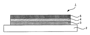
図1は、本発明の有機薄膜太陽電池の一例を示す概略断面図である。図1に示す例において、有機薄膜太陽電池1は、透明基板2と、透明基板2上に形成された第1電極層3と、第1電極層3上に形成された光電変換層4と、光電変換層4上に形成され、金属基材からなる第2電極層5とを有している。光電変換層4および第2電極層5は同面積となっている。
The organic thin-film solar cell of this invention is demonstrated referring drawings.
FIG. 1 is a schematic sectional view showing an example of the organic thin film solar cell of the present invention. In the example shown in FIG. 1, the organic thin film
本発明によれば、第2電極層が金属箔や金属板などの金属基材からなるので、第2電極層側からの水分や酸素の透過を防ぐことができる。したがって、第2電極層によって光電変換層を水分や酸素から保護することができ、光電変換層の劣化を抑制することが可能である。
また本発明によれば、第2電極層が金属基材からなり水分や酸素に対してバリア性を有するので、第2電極層の上から封止基板を用いて封止を行う必要がない。したがって、第1電極層および第2電極層から容易に外部回路に電力を取り出すことが可能である。さらには、有機薄膜太陽電池の構造を単純化することができ、製造工程を簡素化することが可能である。
According to the present invention, since the second electrode layer is made of a metal base material such as a metal foil or a metal plate, permeation of moisture and oxygen from the second electrode layer side can be prevented. Therefore, the photoelectric conversion layer can be protected from moisture and oxygen by the second electrode layer, and deterioration of the photoelectric conversion layer can be suppressed.
According to the present invention, since the second electrode layer is made of a metal base material and has a barrier property against moisture and oxygen, it is not necessary to perform sealing using a sealing substrate from above the second electrode layer. Therefore, it is possible to easily extract electric power from the first electrode layer and the second electrode layer to the external circuit. Furthermore, the structure of the organic thin film solar cell can be simplified, and the manufacturing process can be simplified.
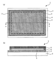
図2(a)、(b)は、本発明の有機薄膜太陽電池の他の例を示す概略平面図および断面図であり、図2(b)は図2(a)のA−A線断面図である。なお、図2(a)において、光電変換層4は一点鎖線、第2電極層5は破線で示されている。図2(a)、(b)に示す有機薄膜太陽電池1は、透明基板2と、透明基板2上に形成された第1電極層3と、第1電極層3上に形成された光電変換層4と、光電変換層4上に形成され、金属基材からなる第2電極層5と、第1電極層3および第2電極層5の間に光電変換層4の外周を囲むように形成された絶縁性を有する接着剤層6とを有している。接着剤層6は絶縁性を有するので、第1電極層3および第2電極層5間で短絡は生じない。
2 (a) and 2 (b) are a schematic plan view and a sectional view showing another example of the organic thin film solar cell of the present invention, and FIG. 2 (b) is a sectional view taken along line AA in FIG. 2 (a). FIG. In FIG. 2A, the
上記有機薄膜太陽電池においては、第1電極層と第2電極層とを接着剤層を介して直接貼り合わせることができる。上述したように、第2電極層が金属基材からなり水分や酸素に対してバリア性を有するため、第2電極層の上から封止基板を用いて封止を行う必要がなく、第1電極層および第2電極層から外部回路に電力を取り出すことができるので、従来のように透明基板と接着剤層との間に電力取り出し用の配線を配置する必要がない。そのため、配線が配置されている部分で気密性が損なわれることもない。また、第1電極層および第2電極層の構成材料はいずれも金属や金属酸化物などの導電性材料であるので、接着剤層は第1電極層および第2電極層のいずれの電極とも接着性が良好である。したがって、接着剤層を形成することにより、密閉性良く光電変換層を封止することができる。よって、光電変換層への水分や酸素の侵入を防ぐことができ、光電変換層の劣化を効果的に抑制することができる。
また、金属基材が金属箔である場合、金属箔は厚みが薄くても水分や酸素に対してバリア性を有するので、フレキシブル性を有する有機薄膜太陽電池とすることができる。したがって、高価なガスバリアフィルムを要することなく、安価にフレキシブル有機薄膜太陽電池を得ることができる。
In the said organic thin film solar cell, a 1st electrode layer and a 2nd electrode layer can be directly bonded together through an adhesive bond layer. As described above, since the second electrode layer is made of a metal base material and has a barrier property against moisture and oxygen, it is not necessary to perform sealing using a sealing substrate from above the second electrode layer. Since electric power can be taken out from the electrode layer and the second electrode layer to the external circuit, it is not necessary to arrange a wiring for taking out electric power between the transparent substrate and the adhesive layer as in the prior art. Therefore, the airtightness is not impaired at the portion where the wiring is arranged. In addition, since the constituent materials of the first electrode layer and the second electrode layer are both conductive materials such as metals and metal oxides, the adhesive layer is bonded to both the first electrode layer and the second electrode layer. Good properties. Therefore, the photoelectric conversion layer can be sealed with good airtightness by forming the adhesive layer. Therefore, intrusion of moisture or oxygen into the photoelectric conversion layer can be prevented, and deterioration of the photoelectric conversion layer can be effectively suppressed.
Further, when the metal substrate is a metal foil, the metal foil has a barrier property against moisture and oxygen even when the metal foil is thin, so that an organic thin film solar cell having flexibility can be obtained. Therefore, a flexible organic thin film solar cell can be obtained at low cost without requiring an expensive gas barrier film.
以下、本発明の有機薄膜太陽電池における各構成について説明する。 Hereinafter, each structure in the organic thin-film solar cell of this invention is demonstrated.
1.第2電極層
本発明における第2電極層は、光電変換層上に形成され、金属基材からなるものである。通常、第2電極層は、光電変換層で発生した電子を取り出すための電極(電子取出し電極)とされる。
1. 2nd electrode layer The 2nd electrode layer in this invention is formed on a photoelectric converting layer, and consists of a metal base material. Usually, the second electrode layer is an electrode for extracting electrons generated in the photoelectric conversion layer (electron extraction electrode).
第2電極層は水分や酸素に対してバリア性を有するものである。第2電極層の水蒸気透過率としては、1×10⁻²g/(m2・day)以下であることが好ましく、中でも1×10-3g/(m2・day)以下、特に1×10-4g/(m2・day)以下であることが好ましい。なお、水蒸気透過率は小さければ小さいほど好ましいので、下限は特に限定されない。また、第2電極層の酸素透過度としては、1×10-4ml/(m2・day)以下であることが好ましい。なお、酸素透過度は小さければ小さいほど好ましいので、下限は特に限定されない。
ここで、水蒸気透過率は、水蒸気透過率測定装置(MOCON社製:PERMATRA)を用いて測定した値である。また、酸素透過度は、酸素ガス透過率測定装置(MOCON社製:OX−TRAN)を用いて測定した値である。
The second electrode layer has a barrier property against moisture and oxygen. The water vapor permeability of the second electrode layer is preferably 1 × 10 −2 g / (m 2 · day) or less, more preferably 1 × 10 −3 g / (m 2 · day) or less, particularly 1 × It is preferably 10 −4 g / (m 2 · day) or less. In addition, since a water vapor permeability is so preferable that it is small, a minimum is not specifically limited. The oxygen permeability of the second electrode layer is preferably 1 × 10 −4 ml / (m 2 · day) or less. In addition, since the oxygen permeability is preferably as small as possible, the lower limit is not particularly limited.
Here, the water vapor transmission rate is a value measured using a water vapor transmission rate measuring device (manufactured by MOCON: PERMATRA). The oxygen permeability is a value measured using an oxygen gas permeability measuring device (manufactured by MOCON: OX-TRAN).
金属基材の形態としては、特に限定されるものではなく、例えば金属箔や金属板が挙げられる。中でも、金属箔が好ましく用いられる。金属基材が金属箔である場合には、安価にフレキシブル性を有する有機薄膜太陽電池を得ることができる。
なお、金属箔とは、フレキシブル性を有するものをいう。また、金属板とは、フレキシブル性を有さないものをいう。
ここで、金属基材がフレキシブル性を有するとは、JIS Z 2248の金属材料曲げ試験方法で、5KNの力をかけたときに曲がることを指す。
It does not specifically limit as a form of a metal base material, For example, metal foil and a metal plate are mentioned. Among these, metal foil is preferably used. When the metal substrate is a metal foil, an organic thin film solar cell having flexibility can be obtained at a low cost.
In addition, metal foil means what has flexibility. Moreover, a metal plate means what does not have flexibility.
Here, that the metal substrate has flexibility refers to bending when a force of 5 KN is applied in the metal material bending test method of JIS Z 2248.
金属基材を構成する金属材料は、電極として機能し、金属箔や金属板となり得るものであり、上述のバリア性を満たすものであれば特に限定されるものではない。中でも、第2電極層が電子取出し電極である場合は、仕事関数の低いものであることが好ましい。具体的には、アルミニウム、銅、チタン、クロム、タングステン、モリブデン、白金、タンタル、ニオブ、ジルコニウム、亜鉛、銀、金、各種ステンレスおよびそれらの合金等が挙げられる。中でも、アルミニウム、銀が好ましい。 The metal material which comprises a metal base material functions as an electrode, can become metal foil and a metal plate, and will not be specifically limited if the above-mentioned barrier property is satisfy | filled. In particular, when the second electrode layer is an electron extraction electrode, it is preferable that the work function is low. Specific examples include aluminum, copper, titanium, chromium, tungsten, molybdenum, platinum, tantalum, niobium, zirconium, zinc, silver, gold, various stainless steels, and alloys thereof. Of these, aluminum and silver are preferable.
金属基材の厚みとしては、電極として機能し、上述のバリア性を満たす金属基材が得られる厚みであれば特に限定されるものではなく、具体的には10μm以上であればよく、10μm〜3mm程度とすることができる。金属基材の厚みが厚いほど、導電性やバリア性に優れたものとなる。一方、金属基材の厚みが薄いほど、フレキシブル性に富んだものとなる。フレキシブル性を考慮すると、金属基材の厚みは、10μm〜300μmの範囲内であることが好ましく、30μm〜300μmの範囲内であることがより好ましい。 The thickness of the metal substrate is not particularly limited as long as the metal substrate functions as an electrode and can provide a metal substrate satisfying the above-described barrier properties. Specifically, the thickness may be 10 μm or more. It can be about 3 mm. The thicker the metal substrate, the better the conductivity and barrier properties. On the other hand, the thinner the metal substrate, the richer the flexibility. Considering flexibility, the thickness of the metal substrate is preferably in the range of 10 μm to 300 μm, and more preferably in the range of 30 μm to 300 μm.
金属基材の作製方法としては、金属基材単体を得る方法であれば特に限定されるものではなく、一般的な方法を用いることができ、金属材料の種類や金属基材の厚みなどに応じて適宜選択される。 The method for producing the metal substrate is not particularly limited as long as it is a method for obtaining a single metal substrate, and a general method can be used, depending on the type of metal material and the thickness of the metal substrate. Are appropriately selected.
第2電極層の形成位置としては、第2電極層が、光電変換層を水分や酸素から保護することができるように光電変換層上に形成され、かつ第1電極層および第2電極層間で短絡が生じないように配置されていれば特に限定されるものではない。例えば、図1に示すように第2電極層5が光電変換層4と同面積となるように形成されていてもよい。この場合、第2電極層および光電変換層が同面積であることにより、第2電極層によって光電変換層を保護することができるとともに、第1電極層および第2電極層間で短絡が生じることもない。また、図2(a)、(b)に示すように第2電極層5が光電変換層4よりも大面積となるように形成され、第2電極層5および第1電極層3の間で光電変換層4が形成されていない部分には絶縁性を有する接着剤層6が形成されていてもよい。この場合、第2電極層が光電変換層よりも大面積であることにより、第2電極層によって光電変換層を保護することができるとともに、絶縁性を有する接着剤層が形成されていることにより、第1電極層および第2電極層間で短絡が生じることもない。
As a formation position of the second electrode layer, the second electrode layer is formed on the photoelectric conversion layer so as to protect the photoelectric conversion layer from moisture and oxygen, and between the first electrode layer and the second electrode layer. If it arrange | positions so that a short circuit may not arise, it will not specifically limit. For example, as shown in FIG. 1, the
第2電極層を光電変換層上に形成する方法としては、金属基材からなる第2電極層を光電変換層上に密着性良く配置することができる方法であれば特に限定されるものではなく、例えば、光電変換層上に金属基材を熱圧着する方法が挙げられる。光電変換層は導電性高分子材料などの有機材料を含有するものであるので、光電変換層上に金属基材を熱ラミネートすることで密着性良く金属基材を積層することができる。 The method for forming the second electrode layer on the photoelectric conversion layer is not particularly limited as long as the second electrode layer made of a metal substrate can be disposed on the photoelectric conversion layer with good adhesion. For example, the method of thermocompression bonding a metal base material on a photoelectric converting layer is mentioned. Since the photoelectric conversion layer contains an organic material such as a conductive polymer material, the metal substrate can be laminated with good adhesion by thermally laminating the metal substrate on the photoelectric conversion layer.
2.接着剤層
本発明においては、上記第1電極層および上記第2電極層の間に、上記光電変換層の外周に沿って、絶縁性を有する接着剤層が形成されていることが好ましい。第1電極層および第2電極層間での短絡を防ぐために、第1電極層および第2電極層の間で光電変換層が形成されていない部分には必ず接着剤層が形成されていることが好ましい。
2. Adhesive layer In the present invention, it is preferable that an insulating adhesive layer is formed between the first electrode layer and the second electrode layer along the outer periphery of the photoelectric conversion layer. In order to prevent a short circuit between the first electrode layer and the second electrode layer, an adhesive layer is always formed in a portion where the photoelectric conversion layer is not formed between the first electrode layer and the second electrode layer. preferable.
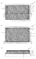
接着剤層の形成位置としては、接着剤層が第1電極層および第2電極層の間に光電変換層の外周に沿って形成され、かつ第1電極層および第2電極層間で短絡が生じないように配置されていれば特に限定されるものではない。例えば、図2(a)、(b)に示すように接着剤層6が第1電極層3および第2電極層5の間に光電変換層4の外周を囲むように形成されていてもよく、図3(a)〜(c)に示すように接着剤層6が第1電極層3および第2電極層5の間に光電変換層4の外周の一部に沿って形成されていてもよい。なお、図3(c)は図3(a)のB−B線断面図および図3(b)C−C線断面図であり、図3(a)、(b)において光電変換層4は一点鎖線、第2電極層5は破線で示されている。また、図示しないが、光電変換層が矩形である場合には、接着剤層が、光電変換層の四辺を囲むように形成されていてもよく、光電変換層の三辺に沿って形成されていてもよく、光電変換層の二辺に沿って形成されていてもよく、光電変換層の一辺に沿って形成されていてもよい。いずれの場合においても、上述したように、第1電極層および第2電極層間での短絡を防ぐために、第1電極層および第2電極層の間で光電変換層が形成されていない部分には必ず接着剤層が形成される。
As the formation position of the adhesive layer, the adhesive layer is formed between the first electrode layer and the second electrode layer along the outer periphery of the photoelectric conversion layer, and a short circuit occurs between the first electrode layer and the second electrode layer. It is not particularly limited as long as it is arranged so that it does not exist. For example, as shown in FIGS. 2A and 2B, the
中でも、接着剤層が光電変換層の外周を囲むように形成されていることが好ましい。第1電極層および第2電極層の密着性を向上させることができるとともに、光電変換層への水分や酸素の侵入を防ぐことができるからである。 Especially, it is preferable that the adhesive layer is formed so as to surround the outer periphery of the photoelectric conversion layer. This is because the adhesion between the first electrode layer and the second electrode layer can be improved, and moisture and oxygen can be prevented from entering the photoelectric conversion layer.
接着剤層に用いられる接着剤としては、絶縁性を有し、第1電極層および第2電極層を貼り合わせることができるものであれば特に限定されるものではなく、例えば、光硬化型樹脂、熱硬化型樹脂、熱可塑型樹脂を用いることができる。中でも、熱硬化型樹脂が好ましく、特に熱硬化型エポキシ樹脂が好ましい。 The adhesive used for the adhesive layer is not particularly limited as long as it has insulating properties and can bond the first electrode layer and the second electrode layer. For example, a photocurable resin A thermosetting resin or a thermoplastic resin can be used. Among these, a thermosetting resin is preferable, and a thermosetting epoxy resin is particularly preferable.
接着剤層の形成方法としては、所望の位置に接着剤層を配置することができる方法であれば特に限定されるものではなく、通常、接着剤を塗布する方法が用いられる。接着剤の塗布方法としては、例えば、インクジェット法、ディスペンサー法、マイクログラビアコート法、グラビアコート法、バーコート法、ロールコート法、ワイヤーバーコート法、ディップコート法、ダイコート法、フレキソ印刷法、オフセット印刷法、スクリーン印刷法等が挙げられる。中でも、インクジェット法、ディスペンサー法、スクリーン印刷法が好ましく用いられる。 The method for forming the adhesive layer is not particularly limited as long as the adhesive layer can be disposed at a desired position, and a method of applying an adhesive is usually used. Examples of the adhesive application method include an inkjet method, a dispenser method, a micro gravure coating method, a gravure coating method, a bar coating method, a roll coating method, a wire bar coating method, a dip coating method, a die coating method, a flexographic printing method, and an offset. Examples thereof include a printing method and a screen printing method. Among these, an inkjet method, a dispenser method, and a screen printing method are preferably used.
接着剤は、第1電極層上に塗布してもよく、第2電極層上に塗布してもよいが、通常は第1電極層上に塗布する。
接着剤が熱硬化型樹脂である場合には、例えば、接着剤の塗布後、光電変換層上に金属基材(第2電極層)を熱圧着し、接着剤を熱硬化させることで、接着剤層を形成することができる。接着剤が熱可塑型樹脂である場合には、例えば、接着剤の塗布後、光電変換層上に金属基材(第2電極層)を熱圧着し、接着剤を加熱して冷却することで、接着剤層を形成することができる。また、接着剤が光硬化型樹脂である場合には、例えば、接着剤の塗布後、光電変換層上に金属基材(第2電極層)を熱圧着し、接着剤を光硬化させることで、接着剤層を形成することができる。接着剤が光硬化型樹脂である場合、接着剤を光硬化させた後に、さらに熱硬化させてもよい。
The adhesive may be applied on the first electrode layer or the second electrode layer, but is usually applied on the first electrode layer.
When the adhesive is a thermosetting resin, for example, after the adhesive is applied, the metal base material (second electrode layer) is thermocompression-bonded on the photoelectric conversion layer, and the adhesive is thermally cured to bond the adhesive. An agent layer can be formed. When the adhesive is a thermoplastic resin, for example, after applying the adhesive, a metal substrate (second electrode layer) is thermocompression-bonded on the photoelectric conversion layer, and the adhesive is heated and cooled. An adhesive layer can be formed. When the adhesive is a photocurable resin, for example, after applying the adhesive, a metal substrate (second electrode layer) is thermocompression-bonded on the photoelectric conversion layer, and the adhesive is photocured. An adhesive layer can be formed. When the adhesive is a photocurable resin, it may be further thermally cured after the adhesive is photocured.
3.光電変換層
本発明に用いられる光電変換層は、第1電極層と第2電極層との間に形成されるものである。なお、「光電変換層」とは、有機薄膜太陽電池の電荷分離に寄与し、生じた電子および正孔を各々反対方向の電極に向かって輸送する機能を有する部材をいう。
3. Photoelectric Conversion Layer The photoelectric conversion layer used in the present invention is formed between the first electrode layer and the second electrode layer. The “photoelectric conversion layer” refers to a member that contributes to charge separation of the organic thin film solar cell and has a function of transporting generated electrons and holes toward electrodes in opposite directions.
光電変換層は、電子受容性および電子供与性の両機能を有する単一の層であってもよく(第1態様)、また電子受容性の機能を有する電子受容性層と電子供与性の機能を有する電子供与性層とが積層されたものであってもよい(第2態様)。以下、各態様について説明する。 The photoelectric conversion layer may be a single layer having both an electron-accepting function and an electron-donating function (first aspect), or an electron-accepting layer having an electron-accepting function and an electron-donating function. A layer in which an electron donating layer having n is laminated may be used (second embodiment). Hereinafter, each aspect will be described.
(1)第1態様
本発明における光電変換層の第1態様は、電子受容性および電子供与性の両機能を有する単一の層であり、電子供与性材料および電子受容性材料を含有するものである。この光電変換層では、光電変換層内で形成されるpn接合を利用して電荷分離が生じるため、単独で光電変換層として機能する。
(1) 1st aspect The 1st aspect of the photoelectric converting layer in this invention is a single layer which has both an electron-accepting function and an electron-donating function, and contains an electron-donating material and an electron-accepting material It is. In this photoelectric conversion layer, since charge separation occurs using a pn junction formed in the photoelectric conversion layer, it functions as a photoelectric conversion layer alone.
電子供与性材料としては、電子供与体としての機能を有するものであれば特に限定されるものではないが、湿式塗工法により成膜可能なものであることが好ましく、中でも電子供与性の導電性高分子材料であることが好ましい。
導電性高分子はいわゆるπ共役高分子であり、炭素−炭素またはヘテロ原子を含む二重結合または三重結合が、単結合と交互に連なったπ共役系から成り立っており、半導体的性質を示すものである。導電性高分子材料は、高分子主鎖内にπ共役が発達しているため主鎖方向への電荷輸送が基本的に有利である。また、導電性高分子の電子伝達機構は、主にπスタッキングによる分子間のホッピング伝導であるため、高分子の主鎖方向のみならず、光電変換層の膜厚方向への電荷輸送も有利である。さらに、導電性高分子材料は、導電性高分子材料を溶媒に溶解もしくは分散させた塗工液を用いることで湿式塗工法により容易に成膜可能であることから、大面積の有機薄膜太陽電池を高価な設備を必要とせず低コストで製造できるという利点がある。
The electron donating material is not particularly limited as long as it has a function as an electron donor, but it is preferable that the material can be formed by a wet coating method. A polymer material is preferred.
The conductive polymer is a so-called π-conjugated polymer, which is composed of a π-conjugated system in which double bonds or triple bonds containing carbon-carbon or hetero atoms are alternately linked to single bonds, and exhibits semiconducting properties. It is. In the conductive polymer material, π conjugation is developed in the polymer main chain, so that charge transport in the main chain direction is basically advantageous. In addition, since the electron transfer mechanism of the conductive polymer is mainly hopping conduction between molecules by π stacking, it is advantageous not only for the main chain direction of the polymer but also for the charge transport in the film thickness direction of the photoelectric conversion layer. is there. Furthermore, since the conductive polymer material can be easily formed by a wet coating method using a coating solution in which the conductive polymer material is dissolved or dispersed in a solvent, a large-area organic thin film solar cell Can be manufactured at low cost without requiring expensive equipment.
電子供与性の導電性高分子材料としては、例えば、ポリフェニレン、ポリフェニレンビニレン、ポリシラン、ポリチオフェン、ポリカルバゾール、ポリビニルカルバゾール、ポルフィリン、ポリアセチレン、ポリピロール、ポリアニリン、ポリフルオレン、ポリビニルピレン、ポリビニルアントラセン、およびこれらの誘導体、ならびにこれらの共重合体、あるいは、フタロシアニン含有ポリマー、カルバゾール含有ポリマー、有機金属ポリマー等を挙げることができる。 Examples of the electron-donating conductive polymer material include polyphenylene, polyphenylene vinylene, polysilane, polythiophene, polycarbazole, polyvinyl carbazole, porphyrin, polyacetylene, polypyrrole, polyaniline, polyfluorene, polyvinyl pyrene, polyvinyl anthracene, and derivatives thereof. And copolymers thereof, or phthalocyanine-containing polymers, carbazole-containing polymers, organometallic polymers, and the like.
上記の中でも、チオフェン−フルオレン共重合体、ポリアルキルチオフェン、フェニレンエチニレン−フェニレンビニレン共重合体、フェニレンエチニレン−チオフェン共重合体、フェニレンエチニレン−フルオレン共重合体、フルオレン−フェニレンビニレン共重合体、チオフェン−フェニレンビニレン共重合体等が好ましく用いられる。これらは、多くの電子受容性材料に対して、エネルギー準位差が適当であるからである。
なお、例えばフェニレンエチニレン−フェニレンビニレン共重合体(Poly[1,4-phenyleneethynylene-1,4-(2,5-dioctadodecyloxyphenylene)-1,4-phenyleneethene-1,2-diyl-1,4-(2,5-dioctadodecyloxyphenylene)ethene-1,2-diyl])の合成方法については、Macromolecules, 35, 3825 (2002) や、Mcromol. Chem. Phys., 202, 2712 (2001) に詳しい。
Among the above, thiophene-fluorene copolymer, polyalkylthiophene, phenylene ethynylene-phenylene vinylene copolymer, phenylene ethynylene-thiophene copolymer, phenylene ethynylene-fluorene copolymer, fluorene-phenylene vinylene copolymer A thiophene-phenylene vinylene copolymer is preferably used. This is because the energy level difference is appropriate for many electron-accepting materials.
For example, a phenylene ethynylene-phenylene vinylene copolymer (Poly [1,4-phenyleneethynylene-1,4- (2,5-dioctadodecyloxyphenylene) -1,4-phenyleneethene-1,2-diyl-1,4- ( 2,5-dioctadodecyloxyphenylene) ethene-1,2-diyl]) is described in detail in Macromolecules, 35, 3825 (2002) and Micromol. Chem. Phys., 202, 2712 (2001).
また、電子受容性材料としては、電子受容体としての機能を有するものであれば特に限定されるものではないが、湿式塗工法により成膜可能なものであることが好ましく、中でも電子受容性の導電性高分子材料であることが好ましい。導電性高分子材料は、上述したような利点を有するからである。 Further, the electron-accepting material is not particularly limited as long as it has a function as an electron acceptor, but it is preferable that it can be formed into a film by a wet coating method. A conductive polymer material is preferable. This is because the conductive polymer material has the advantages as described above.
電子受容性の導電性高分子材料としては、例えば、ポリフェニレンビニレン、ポリフルオレン、およびこれらの誘導体、ならびにこれらの共重合体、あるいは、カーボンナノチューブ、フラーレン誘導体、CN基またはCF3基含有ポリマーおよびそれらの−CF3置換ポリマー等を挙げることができる。ポリフェニレンビニレン誘導体の具体例としては、CN−PPV(Poly[2-Methoxy-5-(2´-ethylhexyloxy)-1,4-(1-cyanovinylene)phenylene])、MEH−CN−PPV(Poly[2-Methoxy-5-(2´-ethylhexyloxy)-1,4-(1-cyanovinylene)phenylene])等が挙げられる。 Examples of the electron-accepting conductive polymer material include polyphenylene vinylene, polyfluorene, and derivatives thereof, and copolymers thereof, or carbon nanotubes, fullerene derivatives, CN group or CF 3 group-containing polymers, and the like. -CF 3 substituted polymer, and the like. Specific examples of the polyphenylene vinylene derivative include CN-PPV (Poly [2-Methoxy-5- (2′-ethylhexyloxy) -1,4- (1-cyanovinylene) phenylene]), MEH-CN-PPV (Poly [2 -Methoxy-5- (2′-ethylhexyloxy) -1,4- (1-cyanovinylene) phenylene]) and the like.
また、電子供与性化合物がドープされた電子受容性材料や、電子受容性化合物がドープされた電子供与性材料等を用いることもできる。中でも、電子供与性化合物もしくは電子受容性化合物がドープされた導電性高分子材料が好ましく用いられる。導電性高分子材料は、高分子主鎖内にπ共役が発達しているため主鎖方向への電荷輸送が基本的に有利であり、また、電子供与性化合物や電子受容性化合物をドープすることによりπ共役主鎖中に電荷が発生し、電気伝導度を大きく増大させることが可能であるからである。 Further, an electron accepting material doped with an electron donating compound, an electron donating material doped with an electron accepting compound, or the like can also be used. Among these, a conductive polymer material doped with an electron donating compound or an electron accepting compound is preferably used. Conductive polymer materials are basically advantageous in charge transport in the direction of the main chain because of the development of π conjugation in the polymer main chain, and are doped with electron-donating compounds and electron-accepting compounds. This is because electric charges are generated in the π-conjugated main chain, and the electrical conductivity can be greatly increased.
電子供与性化合物がドープされる電子受容性の導電性高分子材料としては、上述した電子受容性の導電性高分子材料を挙げることができる。ドープされる電子供与性化合物としては、例えばLi、K、Ca、Cs等のアルカリ金属やアルカリ土類金属のようなルイス塩基を用いることができる。なお、ルイス塩基は電子供与体として作用する。
また、電子受容性化合物がドープされる電子供与性の導電性高分子材料としては、上述した電子供与性の導電性高分子材料を挙げることができる。ドープされる電子受容性化合物としては、例えばFeCl3(III)、AlCl3、AlBr3、AsF6やハロゲン化合物のようなルイス酸を用いることができる。なお、ルイス酸は電子受容体として作用する。
Examples of the electron-accepting conductive polymer material doped with the electron-donating compound include the above-described electron-accepting conductive polymer material. As the electron-donating compound to be doped, for example, a Lewis base such as an alkali metal such as Li, K, Ca, or Cs or an alkaline earth metal can be used. The Lewis base acts as an electron donor.
Examples of the electron-donating conductive polymer material doped with the electron-accepting compound include the above-described electron-donating conductive polymer material. As the electron-accepting compound to be doped, for example, a Lewis acid such as FeCl 3 (III), AlCl 3 , AlBr 3 , AsF 6 or a halogen compound can be used. In addition, Lewis acid acts as an electron acceptor.
光電変換層の膜厚としては、一般的にバルクヘテロ接合型有機薄膜太陽電池において採用されている膜厚を採用することができる。具体的には、0.2nm〜3000nmの範囲内で設定することができ、好ましくは1nm〜600nmの範囲内である。膜厚が上記範囲より厚いと、光電変換層における体積抵抗が高くなる場合があるからである。一方、膜厚が上記範囲より薄いと、光を十分に吸収できない場合があるからである。 As the film thickness of the photoelectric conversion layer, the film thickness generally employed in bulk heterojunction organic thin film solar cells can be employed. Specifically, it can be set within a range of 0.2 nm to 3000 nm, and preferably within a range of 1 nm to 600 nm. This is because when the film thickness is thicker than the above range, the volume resistance in the photoelectric conversion layer may increase. On the other hand, if the film thickness is thinner than the above range, light may not be sufficiently absorbed.
電子供与性材料および電子受容性材料の混合比は、使用する材料の種類により最適な混合比に適宜調整される。 The mixing ratio of the electron-donating material and the electron-accepting material is appropriately adjusted to an optimal mixing ratio depending on the type of material used.
光電変換層を形成する方法としては、所定の膜厚に均一に形成することができる方法であれば特に限定されるものではないが、湿式塗工法が好ましく用いられる。湿式塗工法であれば、大気中で光電変換層を形成することができ、コストの削減が図れるとともに、大面積化が容易だからである。 The method for forming the photoelectric conversion layer is not particularly limited as long as it can be uniformly formed in a predetermined film thickness, but a wet coating method is preferably used. This is because if the wet coating method is used, the photoelectric conversion layer can be formed in the air, and the cost can be reduced and the area can be easily increased.
光電変換層用塗工液の塗布方法としては、光電変換層用塗工液を均一に塗布することができる方法であれば特に限定されるものではなく、例えば、ダイコート法、スピンコート法、ディップコート法、ロールコート法、ビードコート法、スプレーコート法、バーコート法、グラビアコート法、インクジェット法、スクリーン印刷法、オフセット印刷法等を挙げることができる。
中でも、光電変換層用塗工液の塗布方法は、主に塗布量に応じて厚みを調整することが可能な方法であることが好ましい。主に塗布量に応じて厚みを調整することが可能な方法としては、例えば、ダイコート法、ビードコート法、バーコート法、グラビアコート法、インクジェット法、スクリーン印刷法、オフセット印刷法などの印刷法を挙げることができる。印刷法は有機薄膜太陽電池の大面積化に好適である。
The method for applying the photoelectric conversion layer coating solution is not particularly limited as long as it can uniformly apply the photoelectric conversion layer coating solution. For example, a die coating method, a spin coating method, a dip coating method, and the like. Examples thereof include a coating method, a roll coating method, a bead coating method, a spray coating method, a bar coating method, a gravure coating method, an ink jet method, a screen printing method, and an offset printing method.
Especially, it is preferable that the application | coating method of the coating liquid for photoelectric conversion layers is a method which can adjust thickness mainly according to the application amount. Methods that can adjust the thickness mainly according to the coating amount include, for example, a die coating method, a bead coating method, a bar coating method, a gravure coating method, an ink jet method, a screen printing method, and an offset printing method. Can be mentioned. The printing method is suitable for increasing the area of the organic thin film solar cell.
光電変換層用塗工液の塗布後は、形成された塗膜を乾燥する乾燥処理を施してもよい。光電変換層用塗工液に含まれる溶媒等を早期に除去することにより、生産性を向上させることができるからである。
乾燥処理の方法として、例えば、加熱乾燥、送風乾燥、真空乾燥、赤外線加熱乾燥等、一般的な方法を用いることができる。
After application of the coating liquid for photoelectric conversion layer, a drying treatment for drying the formed coating film may be performed. It is because productivity can be improved by removing the solvent etc. which are contained in the coating liquid for photoelectric conversion layers at an early stage.
As a drying method, for example, a general method such as heat drying, air drying, vacuum drying, infrared heat drying, or the like can be used.
(2)第2態様
本発明における光電変換層の第2態様は、電子受容性の機能を有する電子受容性層と電子供与性の機能を有する電子供与性層とが積層されたものである。以下、電子受容性層および電子供与性層について説明する。
(2) Second Aspect In the second aspect of the photoelectric conversion layer in the present invention, an electron accepting layer having an electron accepting function and an electron donating layer having an electron donating function are laminated. Hereinafter, the electron-accepting layer and the electron-donating layer will be described.
(電子受容性層)
本態様に用いられる電子受容性層は、電子受容性の機能を有するものであり、電子受容性材料を含有するものである。
(Electron-accepting layer)
The electron-accepting layer used in this embodiment has an electron-accepting function and contains an electron-accepting material.
電子受容性材料としては、電子受容体としての機能を有するものであれば特に限定されるものではないが、湿式塗工法により成膜可能なものであることが好ましく、中でも電子受容性の導電性高分子材料であることが好ましい。導電性高分子材料は、上述したような利点を有するからである。具体的には、上記第1態様の光電変換層に用いられる電子受容性の導電性高分子材料と同様のものを挙げることができる。 The electron-accepting material is not particularly limited as long as it has a function as an electron acceptor, but is preferably a material that can be formed into a film by a wet coating method. A polymer material is preferred. This is because the conductive polymer material has the advantages as described above. Specific examples include the same electron-accepting conductive polymer materials used for the photoelectric conversion layer of the first aspect.
電子受容性層の膜厚としては、一般的にバイレイヤー型有機薄膜太陽電池において採用されている膜厚を採用することができる。具体的には、0.1nm〜1500nmの範囲内で設定することができ、好ましくは1nm〜300nmの範囲内である。膜厚が上記範囲より厚いと、電子受容性層における体積抵抗が高くなる可能性があるからである。一方、膜厚が上記範囲より薄いと、光を十分に吸収できない場合があるからである。 As the film thickness of the electron-accepting layer, a film thickness generally employed in a bilayer type organic thin film solar cell can be employed. Specifically, it can be set within a range of 0.1 nm to 1500 nm, and preferably within a range of 1 nm to 300 nm. This is because if the film thickness is larger than the above range, the volume resistance in the electron-accepting layer may be increased. On the other hand, if the film thickness is thinner than the above range, light may not be sufficiently absorbed.
電子受容性層の形成方法としては、上記第1態様の光電変換層の形成方法と同様とすることができる。 The method for forming the electron-accepting layer can be the same as the method for forming the photoelectric conversion layer of the first aspect.
(電子供与性層)
本態様に用いられる電子供与性層は、電子供与性の機能を有するものであり、電子供与性材料を含有するものである。
(Electron donating layer)
The electron donating layer used in this embodiment has an electron donating function and contains an electron donating material.
電子供与性材料としては、電子供与体としての機能を有するものであれば特に限定されるものではないが、湿式塗工法により成膜可能なものであることが好ましく、中でも電子供与性の導電性高分子材料であることが好ましい。導電性高分子材料は、上述したような利点を有するからである。具体的には、上記第1態様の光電変換層に用いられる電子供与性の導電性高分子材料と同様のものを挙げることができる。 The electron donating material is not particularly limited as long as it has a function as an electron donor, but it is preferable that the material can be formed by a wet coating method. A polymer material is preferred. This is because the conductive polymer material has the advantages as described above. Specific examples include the same electron donating conductive polymer materials used for the photoelectric conversion layer of the first aspect.
電子供与性層の膜厚としては、一般的にバイレイヤー型有機薄膜太陽電池において採用されている膜厚を採用することができる。具体的には、0.1nm〜1500nmの範囲内で設定することができ、好ましくは1nm〜300nmの範囲内である。膜厚が上記範囲より厚いと、電子供与性層における体積抵抗が高くなる可能性があるからである。一方、膜厚が上記範囲より薄いと、光を十分に吸収できない場合があるからである。 As a film thickness of the electron donating layer, a film thickness generally employed in a bilayer type organic thin film solar cell can be employed. Specifically, it can be set within a range of 0.1 nm to 1500 nm, and preferably within a range of 1 nm to 300 nm. This is because if the film thickness is larger than the above range, the volume resistance in the electron donating layer may be increased. On the other hand, if the film thickness is thinner than the above range, light may not be sufficiently absorbed.
電子供与性層の形成方法としては、上記第1態様の光電変換層の形成方法と同様とすることができる。 The method for forming the electron donating layer can be the same as the method for forming the photoelectric conversion layer of the first aspect.
4.第1電極層
本発明における第1電極層は、透明基板上に形成され、上記第2電極層と対向する電極である。第1電極層は、通常、光電変換層で発生した正孔を取り出すための電極(正孔取出し電極)とされる。本発明においては、第1電極層側が受光面となる。
4). 1st electrode layer The 1st electrode layer in this invention is an electrode which is formed on a transparent substrate and opposes the said 2nd electrode layer. The first electrode layer is usually an electrode for extracting holes generated in the photoelectric conversion layer (hole extraction electrode). In the present invention, the first electrode layer side is the light receiving surface.
第1電極層は、受光面側の電極となるものであれば特に限定されるものではなく、透明電極であってもよく、また透明電極とパターン状の補助電極とが積層されたものであってもよい。
図4に例示するように第1電極層3がパターン状の補助電極3aと透明電極3bとが積層されたものである場合には、透明電極のシート抵抗が比較的高い場合であっても、補助電極のシート抵抗を十分に低くすることで、第1電極層全体としての抵抗を低減することができる。したがって、発生した電力を効率良く集電することができる。
以下、透明電極および補助電極について説明する。
The first electrode layer is not particularly limited as long as it is an electrode on the light receiving surface side, and may be a transparent electrode, or a laminate of a transparent electrode and a patterned auxiliary electrode. May be.
As illustrated in FIG. 4, when the
Hereinafter, the transparent electrode and the auxiliary electrode will be described.
(1)透明電極
本発明に用いられる透明電極は、透明基板上に形成されるものである。
(1) Transparent electrode The transparent electrode used in the present invention is formed on a transparent substrate.
透明電極の構成材料としては、導電性および透明性を有するものであれば特に限定されなく、In−Zn−O(IZO)、In−Sn−O(ITO)、ZnO−Al、Zn−Sn−O等を挙げることができる。中でも、上記第2電極層の構成材料の仕事関数等を考慮して適宜選択することが好ましい。例えば第2電極層の構成材料を仕事関数の低い材料とした場合には、透明電極の構成材料は仕事関数の高い材料であることが好ましい。導電性および透明性を有し、かつ仕事関数の高い材料としては、ITOが好ましく用いられる。 The constituent material of the transparent electrode is not particularly limited as long as it has conductivity and transparency. In—Zn—O (IZO), In—Sn—O (ITO), ZnO—Al, Zn—Sn— O etc. can be mentioned. Among them, it is preferable to select appropriately considering the work function of the constituent material of the second electrode layer. For example, when the constituent material of the second electrode layer is a material having a low work function, the constituent material of the transparent electrode is preferably a material having a high work function. ITO is preferably used as a material having conductivity and transparency and a high work function.
透明電極の全光線透過率は、85%以上であることが好ましく、中でも90%以上、特に92%以上であることが好ましい。透明電極の全光線透過率が上記範囲であることにより、透明電極にて光を十分に透過することができ、光電変換層にて光を効率的に吸収することができるからである。
なお、上記全光線透過率は、可視光領域において、スガ試験機株式会社製 SMカラーコンピュータ(型番:SM−C)を用いて測定した値である。
The total light transmittance of the transparent electrode is preferably 85% or more, more preferably 90% or more, and particularly preferably 92% or more. This is because when the total light transmittance of the transparent electrode is within the above range, light can be sufficiently transmitted through the transparent electrode and light can be efficiently absorbed by the photoelectric conversion layer.
The total light transmittance is a value measured using an SM color computer (model number: SM-C) manufactured by Suga Test Instruments Co., Ltd. in the visible light region.
透明電極のシート抵抗は、20Ω/□以下であることが好ましく、中でも10Ω/□以下、特に5Ω/□以下であることが好ましい。シート抵抗が上記範囲より大きいと、発生した電荷を十分に外部回路へ伝達できない可能性があるからである。
なお、上記シート抵抗は、三菱化学株式会社製 表面抵抗計(ロレスタMCP:四端子プローブ)を用い、JIS R1637(ファインセラミックス薄膜の抵抗率試験方法:4探針法による測定方法)に基づき、測定した値である。
The sheet resistance of the transparent electrode is preferably 20Ω / □ or less, more preferably 10Ω / □ or less, and particularly preferably 5Ω / □ or less. This is because if the sheet resistance is larger than the above range, the generated charge may not be sufficiently transmitted to the external circuit.
In addition, the said sheet resistance is measured based on JIS R1637 (Resistance test method of fine ceramics thin film: Measurement method by 4 probe method) using a surface resistance meter (Loresta MCP: Four-terminal probe) manufactured by Mitsubishi Chemical Corporation. It is the value.
透明電極は、単層であってもよく、また異なる仕事関数の材料を用いて積層されたものであってもよい。
この透明電極の膜厚としては、単層である場合はその膜厚が、複数層からなる場合は総膜厚が、0.1nm〜500nmの範囲内であることが好ましく、中でも1nm〜300nmの範囲内であることが好ましい。膜厚が上記範囲より薄いと、透明電極のシート抵抗が大きくなりすぎ、発生した電荷を十分に外部回路へ伝達できない可能性があり、一方、膜厚が上記範囲より厚いと、全光線透過率が低下し、光電変換効率を低下させる可能性があるからである。
The transparent electrode may be a single layer or may be laminated using materials having different work functions.
As the film thickness of this transparent electrode, the film thickness is preferably in the range of 0.1 nm to 500 nm in the case of a single layer, and the total film thickness is preferably in the range of 0.1 nm to 500 nm. It is preferable to be within the range. If the film thickness is less than the above range, the sheet resistance of the transparent electrode becomes too large, and the generated charge may not be sufficiently transmitted to the external circuit. On the other hand, if the film thickness is thicker than the above range, the total light transmittance This is because there is a possibility that the photoelectric conversion efficiency is lowered.
透明電極の形成方法としては、一般的な電極の形成方法を用いることができる。 As a method for forming the transparent electrode, a general electrode forming method can be used.
(2)補助電極
本発明に用いられる補助電極は、透明基板上にパターン状に形成されるものである。補助電極は、通常、透明電極よりも抵抗値が低い。
(2) Auxiliary electrode The auxiliary electrode used for this invention is formed in a pattern form on a transparent substrate. The auxiliary electrode usually has a lower resistance value than the transparent electrode.
補助電極の形成材料としては、通常、金属が用いられる。補助電極に用いられる金属としては、例えば、アルミニウム(Al)、金(Au)、銀(Ag)、コバルト(Co)、ニッケル(Ni)、白金(Pt)、銅(Cu)、チタン(Ti)、鉄(Fe)、ステンレス系金属、アルミニウム合金、銅合金、チタン合金、鉄−ニッケル合金およびニッケル−クロム合金(Ni−Cr)等の導電性金属を挙げることができる。上述の導電性金属の中でも、電気抵抗値が比較的低いものが好ましい。このような導電性金属としては、Al、Au、Ag、Cu等が挙げられる。 A metal is usually used as a material for forming the auxiliary electrode. Examples of the metal used for the auxiliary electrode include aluminum (Al), gold (Au), silver (Ag), cobalt (Co), nickel (Ni), platinum (Pt), copper (Cu), and titanium (Ti). And conductive metals such as iron (Fe), stainless steel, aluminum alloy, copper alloy, titanium alloy, iron-nickel alloy and nickel-chromium alloy (Ni-Cr). Among the conductive metals described above, those having a relatively low electrical resistance value are preferred. Examples of such a conductive metal include Al, Au, Ag, and Cu.
また、補助電極は、上述のような導電性金属からなる単層であってもよく、また基板や透明電極との密着性向上のために、導電性金属層とコンタクト層とを適宜積層したものであってもよい。コンタクト層の形成材料としては、例えば、ニッケル(Ni)、クロム(Cr)、ニッケルクロム(Ni−Cr)、チタン(Ti)、タンタル(Ta)等が挙げられる。コンタクト層は所望の補助電極と基板や透明電極との密着性を得るために導電性金属層に積層されるものであり、導電性金属層の片側にのみ積層してもよく、導電性金属層の両側に積層してもよい。 In addition, the auxiliary electrode may be a single layer made of the conductive metal as described above, and is formed by appropriately laminating the conductive metal layer and the contact layer in order to improve the adhesion to the substrate or the transparent electrode. It may be. Examples of the material for forming the contact layer include nickel (Ni), chromium (Cr), nickel chromium (Ni—Cr), titanium (Ti), and tantalum (Ta). The contact layer is laminated on the conductive metal layer in order to obtain adhesion between the desired auxiliary electrode and the substrate or the transparent electrode, and may be laminated only on one side of the conductive metal layer. You may laminate on both sides.
また、第2電極層の形成材料の仕事関数等に応じて、好ましい金属を選択してもよい。例えば、第2電極層の形成材料の仕事関数等を考慮する場合には、第1電極層は正孔取出し電極であるので、補助電極に用いられる金属は仕事関数の高いものであることが好ましい。具体的には、Alが好ましく用いられる。 Further, a preferred metal may be selected according to the work function of the material for forming the second electrode layer. For example, when the work function of the material for forming the second electrode layer is taken into consideration, the first electrode layer is a hole extraction electrode, and therefore, the metal used for the auxiliary electrode preferably has a high work function. . Specifically, Al is preferably used.
補助電極の形状としては、パターン状であれば特に限定されるものではなく、所望の導電性、透過性、強度等により適宜選択される。例えば、補助電極は、メッシュ状のメッシュ部と、このメッシュ部の周囲に配置されたフレーム部とを有するものであってもよく、メッシュ状のメッシュ部からなるものであってもよい。 The shape of the auxiliary electrode is not particularly limited as long as it is a pattern, and is appropriately selected depending on desired conductivity, permeability, strength, and the like. For example, the auxiliary electrode may have a mesh-shaped mesh portion and a frame portion arranged around the mesh portion, or may be formed of a mesh-shaped mesh portion.
補助電極がメッシュ部とフレーム部とを有する場合、メッシュ部およびフレーム部の配置としては、例えば補助電極が矩形である場合、フレーム部が、メッシュ部の四方を囲むように配置されていてもよく、メッシュ部の三方を囲むように配置されていてもよく、メッシュ部の二方を囲むように配置されていてもよく、メッシュ部の一方に配置されていてもよい。中でも、フレーム部は、メッシュ部の四方または三方を囲むように配置されていることが好ましい。効率良く集電することができるからである。 When the auxiliary electrode has a mesh portion and a frame portion, the mesh portion and the frame portion may be arranged, for example, when the auxiliary electrode is rectangular, the frame portion may be arranged so as to surround four sides of the mesh portion. Further, it may be arranged so as to surround three sides of the mesh part, may be arranged so as to surround two sides of the mesh part, or may be arranged on one side of the mesh part. Especially, it is preferable that the frame part is arrange | positioned so that the four sides or three sides of a mesh part may be enclosed. This is because current can be collected efficiently.
メッシュ部の形状としては、メッシュ状であれば特に限定されるものではなく、所望の導電性、透過性、強度等により適宜選択される。例えば、三角形、四角形、六角形等の多角形や円形の格子状等が挙げられる。なお、多角形や円形の「格子状」とは、多角形や円形が周期的に配列されている形状をいう。多角形や円形の格子状としては、例えば多角形の開口部がストレートに配列されていてもよく、ジグザグに配列されていてもよい。 The shape of the mesh portion is not particularly limited as long as it is a mesh shape, and is appropriately selected depending on desired conductivity, permeability, strength, and the like. For example, a polygon such as a triangle, a quadrangle, and a hexagon, a circular lattice, and the like can be given. In addition, a polygon or circular “lattice shape” refers to a shape in which polygons or circles are periodically arranged. As the polygonal or circular lattice shape, for example, polygonal openings may be arranged in a straight line or zigzag.
中でも、メッシュ部の形状は、六角形の格子状または平行四辺形の格子状であることが好ましい。メッシュ部を流れる電流が局所的に集中するのを防止することができるからである。六角形の格子状の場合、特に、六角形の開口部がジグザグに(いわゆるハニカム状に)配列されていることが好ましい。一方、平行四辺形の格子状の場合、平行四辺形の鋭角が40°〜80°の範囲内であることが好ましく、より好ましくは50°〜70°の範囲内、さらに好ましくは55°〜65°の範囲内である。 Especially, it is preferable that the shape of a mesh part is a hexagonal lattice shape or a parallelogram lattice shape. This is because the current flowing through the mesh portion can be prevented from being concentrated locally. In the case of a hexagonal lattice, it is particularly preferable that the hexagonal openings are arranged in a zigzag (so-called honeycomb shape). On the other hand, in the case of a parallelogram lattice, the acute angle of the parallelogram is preferably within the range of 40 ° to 80 °, more preferably within the range of 50 ° to 70 °, and even more preferably 55 ° to 65 °. Within the range of °.
補助電極自体は基本的に光を透過しないので、補助電極のメッシュ部の開口部から光電変換層に光が入射する。そのため、補助電極のメッシュ部の開口部は比較的大きいことが好ましい。具体的には、補助電極のメッシュ部の開口部の比率は、50%〜98%程度であることが好ましく、より好ましくは70%〜98%の範囲内、さらに好ましくは80%〜98%の範囲内である。 Since the auxiliary electrode itself basically does not transmit light, light enters the photoelectric conversion layer from the opening of the mesh portion of the auxiliary electrode. Therefore, it is preferable that the opening of the mesh part of the auxiliary electrode is relatively large. Specifically, the ratio of the openings in the mesh portion of the auxiliary electrode is preferably about 50% to 98%, more preferably in the range of 70% to 98%, and still more preferably in the range of 80% to 98%. Within range.
補助電極のメッシュ部の開口部のピッチおよびメッシュ部の線幅は、補助電極全体の面積等に応じて適宜選択される。
また、フレーム部の線幅は、補助電極全体の面積等に応じて適宜選択される。
The pitch of the openings of the mesh portion of the auxiliary electrode and the line width of the mesh portion are appropriately selected according to the area of the entire auxiliary electrode and the like.
The line width of the frame portion is appropriately selected according to the area of the entire auxiliary electrode.
補助電極の厚みは、第1電極層と第2電極層との間で短絡が生じない厚みであれば限定されるものではなく、光電変換層、正孔取出し層、電子取出し層等の厚みに応じて適宜選択される。具体的には、第1電極層と第2電極層との間に形成される層(光電変換層、正孔取出し層、電子取出し層)の総膜厚を1とすると、補助電極の厚みは、5以下であることが好ましく、中でも3以下、さらには2以下、特に1.5以下であることが好ましく、1以下であることが最も好ましい。補助電極の厚みが上記範囲より厚いと、電極間で短絡が生じるおそれがあるからである。より具体的には、補助電極の厚みは、100nm〜1000nmの範囲内であることが好ましく、中でも200nm〜800nmの範囲内、さらには200nm〜500nmの範囲内、特に200nm〜400nmの範囲内であることが好ましい。補助電極の厚みが上記範囲より薄いと、補助電極のシート抵抗が大きくなる場合があるからである。また、補助電極の厚みが上記範囲より厚いと、電極間で短絡が生じるおそれがあるからである。 The thickness of the auxiliary electrode is not limited as long as the short circuit does not occur between the first electrode layer and the second electrode layer, and the thickness of the photoelectric conversion layer, the hole extraction layer, the electron extraction layer, etc. It is selected as appropriate. Specifically, when the total film thickness of the layers (photoelectric conversion layer, hole extraction layer, electron extraction layer) formed between the first electrode layer and the second electrode layer is 1, the thickness of the auxiliary electrode is It is preferably 5 or less, more preferably 3 or less, further 2 or less, particularly preferably 1.5 or less, and most preferably 1 or less. This is because if the thickness of the auxiliary electrode is larger than the above range, a short circuit may occur between the electrodes. More specifically, the thickness of the auxiliary electrode is preferably in the range of 100 nm to 1000 nm, more preferably in the range of 200 nm to 800 nm, further in the range of 200 nm to 500 nm, and particularly in the range of 200 nm to 400 nm. It is preferable. This is because if the thickness of the auxiliary electrode is thinner than the above range, the sheet resistance of the auxiliary electrode may increase. Moreover, it is because there exists a possibility that a short circuit may arise between electrodes when the thickness of an auxiliary electrode is thicker than the said range.
中でも、第1電極層上に、主に塗布量に応じて厚みを調整することが可能な方法により光電変換層を形成する場合、補助電極の厚みは200nm〜300nmの範囲内であることが好ましい。第1電極層上に、主に塗布量に応じて厚みを調整することが可能な方法により光電変換層を形成する場合、補助電極の厚みが上記範囲よりも厚いと、補助電極のメッシュ部やフレーム部のエッジを覆うことが困難となり、電極間で短絡が生じやすくなる。また、補助電極の厚みが上記範囲よりも厚いと、表面張力によって所望の厚みよりも厚く光電変換層が形成されてしまうおそれがある。光電変換層の厚みが厚すぎると、電子拡散長および正孔拡散長を超えてしまい変換効率が低下する。表面張力によって所望の厚みよりも厚く光電変換層が形成されないように、補助電極の厚みを調整することが好ましい。特に、光電変換層内を正孔および電子が移動できる距離は100nm程度であることが知られていることからも、表面張力によって所望の厚みよりも厚く光電変換層が形成されないように、補助電極の厚みを調整することが好ましいのである。
一方、例えばスピンコート法により光電変換層を形成する場合、遠心力により均質な膜とするので、補助電極の厚みが比較的厚くても、補助電極のエッジを覆うことができる。また、スピンコート法の場合、回転数によって厚みを調整することができるので、補助電極の厚みが比較的厚くても、均質な膜を得ることができる。
よって、主に塗布量に応じて厚みを調整することが可能な方法により光電変換層を形成する場合には、上記範囲が特に好ましいのである。
Especially, when forming a photoelectric converting layer on the 1st electrode layer by the method which can adjust thickness mainly according to a coating amount, it is preferable that the thickness of an auxiliary electrode exists in the range of 200 nm-300 nm. . When the photoelectric conversion layer is formed on the first electrode layer by a method capable of adjusting the thickness mainly according to the coating amount, if the thickness of the auxiliary electrode is larger than the above range, the mesh portion of the auxiliary electrode or It becomes difficult to cover the edge of the frame part, and a short circuit is likely to occur between the electrodes. Further, if the thickness of the auxiliary electrode is larger than the above range, the photoelectric conversion layer may be formed thicker than the desired thickness due to surface tension. If the thickness of the photoelectric conversion layer is too thick, it exceeds the electron diffusion length and the hole diffusion length, and the conversion efficiency decreases. It is preferable to adjust the thickness of the auxiliary electrode so that the photoelectric conversion layer is not formed thicker than desired due to surface tension. In particular, since it is known that the distance that holes and electrons can move in the photoelectric conversion layer is about 100 nm, the auxiliary electrode is formed so that the photoelectric conversion layer is not formed thicker than the desired thickness due to surface tension. It is preferable to adjust the thickness.
On the other hand, when the photoelectric conversion layer is formed by, for example, a spin coating method, a uniform film is formed by centrifugal force, so that the edge of the auxiliary electrode can be covered even if the auxiliary electrode is relatively thick. In the case of the spin coating method, the thickness can be adjusted by the number of rotations, so that a uniform film can be obtained even if the auxiliary electrode is relatively thick.
Therefore, when the photoelectric conversion layer is formed mainly by a method capable of adjusting the thickness according to the coating amount, the above range is particularly preferable.
補助電極のシート抵抗としては、透明電極のシート抵抗よりも低ければよい。具体的に、補助電極のシート抵抗は、5Ω/□以下であることが好ましく、中でも3Ω/□以下、さらには1Ω/□以下、特に0.5Ω/□以下であることが好ましく、0.1Ω/□以下であることが最も好ましい。補助電極のシート抵抗が上記範囲より大きいと、所望の発電効率が得られない場合があるからである。
なお、上記シート抵抗は、三菱化学株式会社製 表面抵抗計(ロレスタMCP:四端子プローブ)を用い、JIS R1637(ファインセラミックス薄膜の抵抗率試験方法:4探針法による測定方法)に基づき、測定した値である。
The sheet resistance of the auxiliary electrode may be lower than that of the transparent electrode. Specifically, the sheet resistance of the auxiliary electrode is preferably 5Ω / □ or less, more preferably 3Ω / □ or less, more preferably 1Ω / □ or less, particularly preferably 0.5Ω / □ or less, and 0.1Ω. Most preferably, it is less than / □. This is because if the sheet resistance of the auxiliary electrode is larger than the above range, desired power generation efficiency may not be obtained.
In addition, the said sheet resistance is measured based on JIS R1637 (Resistance test method of fine ceramics thin film: Measurement method by 4 probe method) using a surface resistance meter (Loresta MCP: Four-terminal probe) manufactured by Mitsubishi Chemical Corporation. It is the value.
透明電極および補助電極の積層順としては、透明基板上に補助電極および透明電極の順に積層されていてもよく、透明基板上に透明電極および補助電極の順に積層されていてもよい。中でも、透明基板上に補助電極および透明電極の順に積層されていることが好ましい。透明電極と光電変換層や正孔取出し層等との接触面積が大きい方が、界面の接合性が良く、正孔の移動効率を高くすることができるからである。 As the stacking order of the transparent electrode and the auxiliary electrode, the auxiliary electrode and the transparent electrode may be stacked in this order on the transparent substrate, or the transparent electrode and the auxiliary electrode may be stacked in this order on the transparent substrate. Especially, it is preferable to laminate | stack in order of the auxiliary electrode and the transparent electrode on the transparent substrate. This is because the larger the contact area between the transparent electrode, the photoelectric conversion layer, the hole extraction layer, and the like, the better the interface bondability and the higher the hole transfer efficiency.
補助電極の形成位置としては、接着剤層が形成されている場合には、補助電極は接着剤層と接するように配置されていることが好ましい。金属からなる補助電極と金属基材からなる第2電極層とに接して接着剤層が形成されていることにより、接着力を向上させることができるからである。
透明基板上に透明電極および補助電極の順に積層されている場合には、補助電極を接着剤層と接するように配置することができる。また、例えば図4に示すように、透明基板上に補助電極3aおよび透明電極3bの順に積層されている場合には、補助電極3a上に透明電極3bが積層されていない領域を設けることにより、補助電極3aを接着剤層6と接するように配置することができる。
As a position where the auxiliary electrode is formed, when the adhesive layer is formed, the auxiliary electrode is preferably disposed so as to be in contact with the adhesive layer. This is because the adhesive force can be improved by forming the adhesive layer in contact with the auxiliary electrode made of metal and the second electrode layer made of the metal substrate.
When the transparent electrode and the auxiliary electrode are laminated in this order on the transparent substrate, the auxiliary electrode can be disposed so as to be in contact with the adhesive layer. For example, as shown in FIG. 4, when the
補助電極の形成方法としては、特に限定されるものではなく、例えば、金属薄膜を全面に成膜した後に網目状にパターニングする方法、網目状の導電体を直接形成する方法等が挙げられる。これらの方法は、補助電極の形成材料や構成等に応じて適宜選択される。 The method for forming the auxiliary electrode is not particularly limited, and examples thereof include a method of forming a metal thin film on the entire surface and then patterning it into a mesh shape, a method of directly forming a mesh-like conductor, and the like. These methods are appropriately selected depending on the auxiliary electrode forming material, configuration, and the like.
金属薄膜の成膜方法としては、真空蒸着法、スパッタリング法、イオンプレーティング法等の真空成膜法であることが好ましい。すなわち、補助電極は真空成膜法にて形成された金属薄膜であることが好ましい。真空成膜法により成膜した金属種は、めっき膜に比べ介在物が少なく比抵抗を小さくでき、またAgペースト等を用いて成膜したものと比較しても比抵抗を小さくできる。また、厚み1μm以下、好ましくは500nm以下の金属薄膜を、膜厚を精密に制御し、均一な厚みに成膜する方法としても、真空成膜法が好適である。
金属薄膜のパターニング方法としては、所望のパターンに精度良く形成することができる方法であれば特に限定されるものではなく、例えばフォトエッチング法等を挙げることができる。
The method for forming the metal thin film is preferably a vacuum film forming method such as a vacuum deposition method, a sputtering method, or an ion plating method. That is, the auxiliary electrode is preferably a metal thin film formed by a vacuum film forming method. The metal species formed by the vacuum film formation method has less inclusions than the plating film and can reduce the specific resistance, and can also reduce the specific resistance as compared with those formed using Ag paste or the like. Further, a vacuum film formation method is also suitable as a method for forming a metal thin film having a thickness of 1 μm or less, preferably 500 nm or less, with a precise thickness and a uniform thickness.
The method for patterning the metal thin film is not particularly limited as long as it can be accurately formed into a desired pattern, and examples thereof include a photoetching method.
5.透明基板
本発明に用いられる透明基板としては、特に限定されるものではなく、例えば石英ガラス、パイレックス(登録商標)、合成石英板等の可撓性のない透明なリジット材、あるいは透明樹脂フィルム、光学用樹脂板等の可撓性を有する透明なフレキシブル材を挙げることができる。
中でも、透明基板が透明樹脂フィルム等のフレキシブル材であることが好ましい。透明樹脂フィルムは、加工性に優れており、製造コスト低減や軽量化、割れにくい有機薄膜太陽電池の実現において有用であり、曲面への適用等、種々のアプリケーションへの適用可能性が広がるからである。
5. Transparent substrate The transparent substrate used in the present invention is not particularly limited. For example, a transparent rigid material having no flexibility such as quartz glass, Pyrex (registered trademark), synthetic quartz plate, or a transparent resin film, Examples thereof include a transparent flexible material having flexibility such as an optical resin plate.
Especially, it is preferable that a transparent substrate is flexible materials, such as a transparent resin film. Transparent resin films are excellent in processability, and are useful in the realization of organic thin-film solar cells that reduce manufacturing costs, reduce weight, and are difficult to break, and expand their applicability to various applications such as application to curved surfaces. is there.
6.正孔取出し層
本発明においては、図5に例示するように、光電変換層4と第1電極層3との間に正孔取出し層7が形成されていてもよい。正孔取出し層は、光電変換層から正孔取出し電極への正孔の取出しが容易に行われるように設けられる層である。これにより、光電変換層から正孔取出し電極への正孔取出し効率が高められるため、光電変換効率を向上させることが可能となる。
6). Hole Extraction Layer In the present invention, as illustrated in FIG. 5, a hole extraction layer 7 may be formed between the
正孔取出し層に用いられる材料としては、光電変換層から正孔取出し電極への正孔の取出しを安定化させる材料であれば特に限定されるものではない。具体的には、ドープされたポリアニリン、ポリフェニレンビニレン、ポリチオフェン、ポリピロール、ポリパラフェニレン、ポリアセチレン、トリフェニルジアミン(TPD)等の導電性有機化合物、またはテトラチオフルバレン、テトラメチルフェニレンジアミン等の電子供与性化合物と、テトラシアノキノジメタン、テトラシアノエチレン等の電子受容性化合物とからなる電荷移動錯体を形成する有機材料等を挙げることができる。また、Au、In、Ag、Pd等の金属等の薄膜も使用することができる。さらに、金属等の薄膜は、単独で形成してもよく、上記の有機材料と組み合わせて用いてもよい。
これらの中でも、特にポリエチレンジオキシチオフェン(PEDOT)、トリフェニルジアミン(TPD)が好ましく用いられる。
The material used for the hole extraction layer is not particularly limited as long as it is a material that stabilizes the extraction of holes from the photoelectric conversion layer to the hole extraction electrode. Specifically, doped polyaniline, polyphenylene vinylene, polythiophene, polypyrrole, polyparaphenylene, polyacetylene, conductive organic compounds such as triphenyldiamine (TPD), or electron donation such as tetrathiofulvalene, tetramethylphenylenediamine, etc. An organic material that forms a charge transfer complex composed of an organic compound and an electron-accepting compound such as tetracyanoquinodimethane and tetracyanoethylene. Also, a thin film of metal such as Au, In, Ag, Pd, etc. can be used. Furthermore, a thin film of metal or the like may be formed alone or in combination with the above organic material.
Among these, polyethylenedioxythiophene (PEDOT) and triphenyldiamine (TPD) are particularly preferably used.
正孔取出し層の膜厚としては、上記有機材料を用いた場合は、10nm〜200nmの範囲内であることが好ましく、上記金属薄膜である場合は、0.1nm〜5nmの範囲内であることが好ましい。 The film thickness of the hole extraction layer is preferably in the range of 10 nm to 200 nm when the organic material is used, and in the range of 0.1 nm to 5 nm in the case of the metal thin film. Is preferred.
7.電子取出し層
本発明においては、図5に例示するように、光電変換層4と第2電極層5との間に電子取出し層8が形成されていてもよい。電子取出し層は、光電変換層から電子取出し電極への電子の取出しが容易に行われるように設けられる層である。これにより、光電変換層から電子取出し電極への電子取出し効率が高められるため、光電変換効率を向上させることが可能となる。
7). Electron Extraction Layer In the present invention, as illustrated in FIG. 5, an electron extraction layer 8 may be formed between the
電子取出し層に用いられる材料としては、光電変換層から電子取出し電極への電子の取出しを安定化させる材料であれば特に限定されない。具体的には、ドープされたポリアニリン、ポリフェニレンビニレン、ポリチオフェン、ポリピロール、ポリパラフェニレン、ポリアセチレン、トリフェニルジアミン(TPD)等の導電性有機化合物、またはテトラチオフルバレン、テトラメチルフェニレンジアミン等の電子供与性化合物と、テトラシアノキノジメタン、テトラシアノエチレン等の電子受容性化合物とからなる電荷移動錯体を形成する有機材料等を挙げることができる。また、アルカリ金属あるいはアルカリ土類金属との金属ドープ層が挙げられる。好適な材料としては、バソキュプロイン(BCP)または、バソフェナントロン(Bphen)と、Li、Cs、Ba、Srなどの金属ドープ層が挙げられる。 The material used for the electron extraction layer is not particularly limited as long as it is a material that stabilizes the extraction of electrons from the photoelectric conversion layer to the electron extraction electrode. Specifically, doped polyaniline, polyphenylene vinylene, polythiophene, polypyrrole, polyparaphenylene, polyacetylene, conductive organic compounds such as triphenyldiamine (TPD), or electron donation such as tetrathiofulvalene, tetramethylphenylenediamine, etc. An organic material that forms a charge transfer complex composed of an organic compound and an electron-accepting compound such as tetracyanoquinodimethane and tetracyanoethylene. Moreover, the metal dope layer with an alkali metal or alkaline-earth metal is mentioned. Suitable materials include bathocuproin (BCP) or bathophenantrone (Bphen) and metal doped layers such as Li, Cs, Ba, Sr.
8.その他の構成
本発明の有機薄膜太陽電池は、上述した構成部材の他にも、必要に応じて後述する構成部材を有していてもよい。例えば、本発明の有機薄膜太陽電池は、保護シート、充填材層、バリア層、保護ハードコート層、強度支持層、防汚層、高光反射層、光封じ込め層、封止材層等の機能層を有していてもよい。また、層構成に応じて、各機能層間に接着層が形成されていてもよい。
なお、これらの機能層については、特開2007−73717号公報等に記載のものと同様とすることができる。
8). Other Configurations The organic thin film solar cell of the present invention may have constituent members to be described later as necessary in addition to the constituent members described above. For example, the organic thin film solar cell of the present invention is a functional layer such as a protective sheet, a filler layer, a barrier layer, a protective hard coat layer, a strength support layer, an antifouling layer, a high light reflection layer, a light containment layer, a sealing material layer, etc. You may have. In addition, an adhesive layer may be formed between the functional layers depending on the layer configuration.
These functional layers can be the same as those described in JP-A-2007-73717.
本発明においては、上述したように第1電極層および第2電極層から容易に外部回路に電力を取り出すことが可能である。例えば、第1電極層および第2電極層の表面にそれぞれ金属製の正極および負極の各端子を接触させることにより、外部回路に電力を取り出すことができる。 In the present invention, as described above, power can be easily taken out from the first electrode layer and the second electrode layer to the external circuit. For example, electric power can be taken out to an external circuit by bringing metallic positive and negative terminals into contact with the surfaces of the first electrode layer and the second electrode layer, respectively.
B.有機薄膜太陽電池モジュール
本発明の有機薄膜太陽電池モジュールは、上述の有機薄膜太陽電池が複数個直列または並列に接続されていることを特徴とするものである。
B. Organic thin film solar cell module The organic thin film solar cell module of the present invention is characterized in that a plurality of the above organic thin film solar cells are connected in series or in parallel.
図6は、本発明の有機薄膜太陽電池モジュールの一例を示す概略断面図である。図6に示す有機薄膜太陽電池モジュール10においては、3個のセル(有機薄膜太陽電池1)が直列に接続されている。各セル(有機薄膜太陽電池1)は、透明基板2と、透明基板2上に形成された第1電極層3と、第1電極層3上に形成された光電変換層4と、光電変換層4上に形成され、金属基材からなる第2電極層5と、第1電極層3および第2電極層5の間に光電変換層4の外周を囲むように形成された絶縁性を有する接着剤層6とを有している。
FIG. 6 is a schematic cross-sectional view showing an example of the organic thin film solar cell module of the present invention. In the organic thin film
上記有機薄膜太陽電池モジュールにおいては、絶縁性を有する接着剤層が形成されていることにより、セル内にて第1電極層および第2電極層間で短絡は生じない。また、絶縁性を有する接着剤層が形成されていることにより、隣接するセル間にて第1電極層同士および第2電極層同士での短絡はない。 In the organic thin film solar cell module, since the insulating adhesive layer is formed, no short circuit occurs between the first electrode layer and the second electrode layer in the cell. Moreover, since the insulating adhesive layer is formed, there is no short circuit between the first electrode layers and between the second electrode layers between adjacent cells.
本発明によれば、上述の有機薄膜太陽電池を有するので、第2電極層の上から封止基板を用いて封止を行う必要がなく、第1電極層および第2電極層から容易に外部回路に電力を取り出すことができるだけでなく、第1電極層および第2電極層を利用して複数個の有機薄膜太陽電池を容易に接続することができる。 According to the present invention, since the organic thin film solar cell described above is included, it is not necessary to perform sealing using a sealing substrate from above the second electrode layer, and the first electrode layer and the second electrode layer can be easily externally connected. Not only can electric power be taken out of the circuit, but also a plurality of organic thin-film solar cells can be easily connected using the first electrode layer and the second electrode layer.
複数個の有機薄膜太陽電池の接続としては、所望の起電力を得ることができればよく、直列のみであってもよく、並列のみであってもよく、直列および並列を組み合わせてもよい。また、同一の透明基板上に複数個の有機薄膜太陽電池が形成され接続されていてもよく、それぞれ別個独立に作製された有機薄膜太陽電池が配線等によって接続されていてもよい。 The connection of the plurality of organic thin-film solar cells is not limited as long as a desired electromotive force can be obtained, may be only in series, may be only in parallel, or may be a combination of series and parallel. In addition, a plurality of organic thin film solar cells may be formed and connected on the same transparent substrate, and organic thin film solar cells separately produced independently may be connected by wiring or the like.
なお、有機薄膜太陽電池については、「A.有機薄膜太陽電池」の項に詳しく記載したので、ここでの説明は省略する。 Since the organic thin film solar cell is described in detail in the section “A. Organic thin film solar cell”, description thereof is omitted here.
本発明は、上記実施形態に限定されるものではない。上記実施形態は例示であり、本発明の特許請求の範囲に記載された技術的思想と実質的に同一な構成を有し、同様な作用効果を奏するものは、いかなるものであっても本発明の技術的範囲に包含される。 The present invention is not limited to the above embodiment. The above-described embodiment is an exemplification, and the present invention has any configuration that has substantially the same configuration as the technical idea described in the claims of the present invention and that exhibits the same effects. Are included in the technical scope.
以下、実施例を挙げて本発明を具体的に説明する。
[実施例1]
厚み125μmのPETフィルム基板の上にPVD法によりSiO2の薄膜を形成し、その上面に圧力勾配型プラズマガンを用いた反応性イオンプレーティング法(パワー:3.7kW、酸素分圧:73%、製膜圧力:0.3Pa、製膜レート:150nm/min、基板温度:20℃)により透明電極であるITO膜(膜厚:150nm、シート抵抗:20Ω/□)を成膜した。
Hereinafter, the present invention will be specifically described with reference to examples.
[Example 1]
A reactive ion plating method using a pressure gradient plasma gun (power: 3.7 kW, oxygen partial pressure: 73%) on a PET film substrate having a thickness of 125 μm by forming a thin film of SiO 2 by PVD method. An ITO film (film thickness: 150 nm, sheet resistance: 20Ω / □), which is a transparent electrode, was formed at a film forming pressure of 0.3 Pa, a film forming rate of 150 nm / min, and a substrate temperature of 20 ° C.
次に、上記ITO膜が形成された基板をアセトン、基板洗浄液、IPAを用いて洗浄した。次に、このITO膜上に、ITO膜の面積よりも大きい面積となるように、かつ、ITO膜の一部が露出するように、導電性高分子ペースト(ポリ−(3,4−エチレンジオキシチオフェン)分散品)を製膜し、100℃で10分間乾燥させ、バッファー層を形成した。 Next, the substrate on which the ITO film was formed was cleaned using acetone, a substrate cleaning solution, and IPA. Next, a conductive polymer paste (poly- (3,4-ethylenedioxide) is formed on the ITO film so that the area is larger than the area of the ITO film and a part of the ITO film is exposed. Oxythiophene) dispersion) was formed into a film and dried at 100 ° C. for 10 minutes to form a buffer layer.
次に、ポリチオフェン(P3HT:poly(3-hexylthiophene-2,5-diyl))とC60PCBM([6,6]-phenyl-C61-butyric acid mettric ester:Nano-C社製)をブロモベンゼンに溶解させ、固形分濃度1.4wt%の光電変換層用塗工液を準備した。次に、同溶液を上記バッファー層上にバッファー層と同じ面積となるようにバーコート法にて塗布し、100℃で10分間乾燥させて、光電変換層を形成した。 Next, polythiophene (P3HT: poly (3-hexylthiophene-2,5-diyl)) and C60PCBM ([6,6] -phenyl-C61-butyric acid mettric ester: manufactured by Nano-C) are dissolved in bromobenzene. A coating solution for a photoelectric conversion layer having a solid content concentration of 1.4 wt% was prepared. Next, the same solution was applied onto the buffer layer by a bar coating method so as to have the same area as the buffer layer, and dried at 100 ° C. for 10 minutes to form a photoelectric conversion layer.
次に、上記ITO膜のバッファー層および光電変換層が形成されていない部分に、熱硬化型エポキシ樹脂を含む絶縁性接着剤を塗布した。
次に、上記光電変換層上に厚み10μmのアルミニウム板を熱ラミネート法にて積層して、金属電極とした。その後、絶縁性接着剤を熱硬化させた。これにより、ITO膜とアルミニウム板の接触部分は絶縁性接着剤を用いて接着された。
得られた有機薄膜太陽電池では、ITO膜に正極用の金属クリップ、アルミニウム板に負極用の金属クリップを接触させることにより、外部回路に電力を取り出した。
Next, an insulating adhesive containing a thermosetting epoxy resin was applied to a portion of the ITO film where the buffer layer and the photoelectric conversion layer were not formed.
Next, an aluminum plate having a thickness of 10 μm was laminated on the photoelectric conversion layer by a heat laminating method to obtain a metal electrode. Thereafter, the insulating adhesive was thermally cured. Thereby, the contact part of an ITO film | membrane and an aluminum plate was adhere | attached using the insulating adhesive agent.
In the obtained organic thin film solar cell, electric power was taken out to the external circuit by bringing the metal clip for the positive electrode into contact with the ITO film and the metal clip for the negative electrode with the aluminum plate.
1 … 有機薄膜太陽電池
2 … 透明基板
3 … 第1電極層
3a … 補助電極
3b … 透明電極
4 … 光電変換層
5 … 第2電極層
6 … 接着剤層
7 … 正孔取出し層
8 … 電子取出し層
10 … 有機薄膜太陽電池モジュール
DESCRIPTION OF
Claims (2)
前記補助電極が、メッシュ部と、前記メッシュ部の周囲に配置されたフレーム部とを有するものであり、
前記透明基板上に、前記補助電極が前記接着剤層に接するように、前記透明電極および前記補助電極を積層する第1電極層形成工程と、
前記第1電極層上に前記光電変換層を形成する光電変換層形成工程と、
前記第1電極層の前記補助電極上または前記第2電極層上に、前記光電変換層の外周を囲むように接着剤を塗布する接着剤塗布工程と、
前記接着剤塗布工程後に、有機材料を含有する前記光電変換層上に前記金属基材を熱圧着する第2電極層形成工程と、
前記接着剤により前記第1電極層の前記補助電極および前記第2電極層を貼り合せる接着工程と
を有することを特徴とする有機薄膜太陽電池の製造方法。 A transparent substrate, a first electrode layer formed on the transparent substrate , the transparent electrode and an auxiliary electrode made of a patterned metal laminated in random order, a photoelectric conversion layer formed on the first electrode layer, The auxiliary electrode is formed on the photoelectric conversion layer and surrounds the outer periphery of the photoelectric conversion layer between the second electrode layer made of a metal base material and the first electrode layer and the second electrode layer. And an organic thin film solar cell manufacturing method having an insulating adhesive layer formed so as to be in contact with the second electrode layer ,
The auxiliary electrode has a mesh part and a frame part arranged around the mesh part,
A first electrode layer forming step of laminating the transparent electrode and the auxiliary electrode such that the auxiliary electrode is in contact with the adhesive layer on the transparent substrate;
A photoelectric conversion layer forming step of forming the photoelectric conversion layer on the first electrode layer;
An adhesive application step of applying an adhesive on the auxiliary electrode or the second electrode layer of the first electrode layer so as to surround an outer periphery of the photoelectric conversion layer;
A second electrode layer forming step of thermocompression bonding the metal substrate on the photoelectric conversion layer containing an organic material after the adhesive application step ;
A method for producing an organic thin-film solar cell, comprising: an adhesion step of bonding the auxiliary electrode and the second electrode layer of the first electrode layer with the adhesive .
Priority Applications (3)
| Application Number | Priority Date | Filing Date | Title |
|---|---|---|---|
| JP2010002128A JP4935910B2 (en) | 2010-01-07 | 2010-01-07 | Organic thin film solar cell |
| PCT/JP2010/071024 WO2011083636A1 (en) | 2010-01-07 | 2010-11-25 | Organic thin film solar cell |
| US13/519,629 US20120298174A1 (en) | 2010-01-07 | 2010-11-25 | Organic thin film solar cell |
Applications Claiming Priority (1)
| Application Number | Priority Date | Filing Date | Title |
|---|---|---|---|
| JP2010002128A JP4935910B2 (en) | 2010-01-07 | 2010-01-07 | Organic thin film solar cell |
Related Child Applications (1)
| Application Number | Title | Priority Date | Filing Date |
|---|---|---|---|
| JP2011237490A Division JP5146584B2 (en) | 2011-10-28 | 2011-10-28 | Organic thin film solar cell |
Publications (3)
| Publication Number | Publication Date |
|---|---|
| JP2011142217A JP2011142217A (en) | 2011-07-21 |
| JP2011142217A5 JP2011142217A5 (en) | 2011-09-15 |
| JP4935910B2 true JP4935910B2 (en) | 2012-05-23 |
Family
ID=44305375
Family Applications (1)
| Application Number | Title | Priority Date | Filing Date |
|---|---|---|---|
| JP2010002128A Expired - Fee Related JP4935910B2 (en) | 2010-01-07 | 2010-01-07 | Organic thin film solar cell |
Country Status (3)
| Country | Link |
|---|---|
| US (1) | US20120298174A1 (en) |
| JP (1) | JP4935910B2 (en) |
| WO (1) | WO2011083636A1 (en) |
Families Citing this family (11)
| Publication number | Priority date | Publication date | Assignee | Title |
|---|---|---|---|---|
| JP5421218B2 (en) * | 2010-10-26 | 2014-02-19 | 出光興産株式会社 | Photoelectric conversion device and method for manufacturing photoelectric conversion device |
| WO2013040036A1 (en) * | 2011-09-13 | 2013-03-21 | University Of Maine System Board Of Trustees | Photovoltaic textiles |
| KR101477953B1 (en) * | 2013-04-01 | 2014-12-30 | 주식회사 엘지화학 | Organic light emitting device and method for manufacturing the same |
| JP6095488B2 (en) * | 2013-05-31 | 2017-03-15 | 三井化学株式会社 | Manufacturing method of organic thin film solar cell |
| CN103594632B (en) * | 2013-11-06 | 2017-02-08 | 华中科技大学 | Composite transparent electrode and organic solar cell including same |
| KR102144478B1 (en) * | 2013-11-12 | 2020-08-14 | 삼성디스플레이 주식회사 | Touch panel and method of preparing touch panel |
| JP6769739B2 (en) * | 2015-05-19 | 2020-10-14 | ローム株式会社 | Manufacturing method of organic thin-film solar cell module, electronic equipment and organic thin-film solar cell module |
| WO2016186166A1 (en) * | 2015-05-19 | 2016-11-24 | ローム株式会社 | Organic thin film solar cell module, electronic device and method for manufacturing organic thin film solar cell module |
| US20190013155A1 (en) * | 2016-02-19 | 2019-01-10 | Sekisui Chemical Co., Ltd. | Solid junction-type photovoltaic device and method for producing same |
| US9978532B2 (en) * | 2016-05-09 | 2018-05-22 | Solar-Tectic Llc | Maximizing the power conversion efficiency of a tin perovskite/silicon thin-film tandem solar cell |
| CN113169277A (en) * | 2018-11-26 | 2021-07-23 | 住友化学株式会社 | Method for manufacturing organic photoelectric conversion element |
Family Cites Families (28)
| Publication number | Priority date | Publication date | Assignee | Title |
|---|---|---|---|---|
| JPS6176695A (en) * | 1984-09-21 | 1986-04-19 | Mitsubishi Metal Corp | Electrolyzing method of tin, lead or tin-lead containing alloy |
| JPS6176695U (en) * | 1984-10-25 | 1986-05-23 | ||
| JPS61138196A (en) * | 1984-12-11 | 1986-06-25 | 株式会社東芝 | Direction controller for hydraulic pressure controller |
| JPS61138196U (en) * | 1985-02-15 | 1986-08-27 | ||
| JPH0799699B2 (en) * | 1987-03-19 | 1995-10-25 | 三洋電機株式会社 | Photoelectric conversion element |
| JPH065730B2 (en) * | 1989-04-24 | 1994-01-19 | 工業技術院長 | Method for producing photoelectric response element using functional protein complex |
| JPH0335566A (en) * | 1989-06-30 | 1991-02-15 | Konica Corp | Photoelectric conversion element |
| JP3069160B2 (en) * | 1991-07-26 | 2000-07-24 | 松下電器産業株式会社 | Polymer solar cells |
| JP3083184B2 (en) * | 1991-09-13 | 2000-09-04 | 東洋化工株式会社 | Photovoltaic organic photoelectric conversion device |
| US6420031B1 (en) * | 1997-11-03 | 2002-07-16 | The Trustees Of Princeton University | Highly transparent non-metallic cathodes |
| JP4441102B2 (en) * | 1999-11-22 | 2010-03-31 | キヤノン株式会社 | Photovoltaic element and manufacturing method thereof |
| JP4477729B2 (en) * | 2000-01-19 | 2010-06-09 | シャープ株式会社 | Photoelectric conversion element and solar cell using the same |
| US7022910B2 (en) * | 2002-03-29 | 2006-04-04 | Konarka Technologies, Inc. | Photovoltaic cells utilizing mesh electrodes |
| US6949400B2 (en) * | 2002-01-25 | 2005-09-27 | Konarka Technologies, Inc. | Ultrasonic slitting of photovoltaic cells and modules |
| US20070251570A1 (en) * | 2002-03-29 | 2007-11-01 | Konarka Technologies, Inc. | Photovoltaic cells utilizing mesh electrodes |
| NL1020744C2 (en) * | 2002-06-04 | 2003-12-08 | Stichting Energie | Liquid-containing photovoltaic element. |
| JP2004158661A (en) * | 2002-11-07 | 2004-06-03 | Matsushita Electric Ind Co Ltd | Organic light to electricity transducing device and its manufacturing method |
| JP5350587B2 (en) * | 2003-03-24 | 2013-11-27 | メルク パテント ゲーエムベーハー | Photoelectric cell with mesh electrode |
| US20040211458A1 (en) * | 2003-04-28 | 2004-10-28 | General Electric Company | Tandem photovoltaic cell stacks |
| BRPI0412045A (en) * | 2003-10-06 | 2006-08-15 | Ngk Spark Plug Co | dye sensitized solar cell |
| TW200715634A (en) * | 2005-07-14 | 2007-04-16 | Konarka Technologies Inc | Stable organic devices |
| JP4771814B2 (en) * | 2006-01-23 | 2011-09-14 | 日東電工株式会社 | Organic photoelectric conversion element |
| TW200818981A (en) * | 2006-08-30 | 2008-04-16 | Sumitomo Chemical Co | Organic electroluminescence device |
| EP1936644A3 (en) * | 2006-12-22 | 2011-01-05 | Sony Deutschland Gmbh | A photovoltaic cell |
| WO2008122027A2 (en) * | 2007-04-02 | 2008-10-09 | Konarka Technologies, Inc. | Novel electrode |
| KR100971113B1 (en) * | 2007-11-23 | 2010-07-20 | 한국과학기술연구원 | Method for fabricating organic photovoltaic device with improved conversion efficiency by partitioned active area and organic photovoltaic device fabricated thereby |
| CN101939875A (en) * | 2008-02-25 | 2011-01-05 | 株式会社藤仓 | Opposing electrode and photoelectric conversion element using the opposing electrode |
| WO2009157304A1 (en) * | 2008-06-23 | 2009-12-30 | シャープ株式会社 | Solar cell, photoconcentration-type photovoltaic module, and method for manufacturing solar cell |
-
2010
- 2010-01-07 JP JP2010002128A patent/JP4935910B2/en not_active Expired - Fee Related
- 2010-11-25 US US13/519,629 patent/US20120298174A1/en not_active Abandoned
- 2010-11-25 WO PCT/JP2010/071024 patent/WO2011083636A1/en active Application Filing
Also Published As
| Publication number | Publication date |
|---|---|
| US20120298174A1 (en) | 2012-11-29 |
| WO2011083636A1 (en) | 2011-07-14 |
| JP2011142217A (en) | 2011-07-21 |
Similar Documents
| Publication | Publication Date | Title |
|---|---|---|
| JP4935910B2 (en) | Organic thin film solar cell | |
| JP4985717B2 (en) | Organic thin film solar cell and method for producing the same | |
| JP5265076B2 (en) | Photovoltaic component and method of manufacturing the same | |
| JP4905595B2 (en) | Organic thin film solar cell, organic thin film solar cell module, and organic thin film solar cell manufacturing method | |
| JP5007772B2 (en) | Organic solar cell module and organic solar cell panel | |
| JP5146584B2 (en) | Organic thin film solar cell | |
| JP5326731B2 (en) | Organic thin film solar cell | |
| JP2009076668A (en) | Organic thin-film solar cell | |
| JP2011151195A (en) | Organic thin film solar cell, and method of manufacturing the same | |
| JP5573372B2 (en) | Organic thin film solar cell and method for producing the same | |
| JP5789971B2 (en) | Manufacturing method of organic thin film solar cell | |
| WO2011074306A1 (en) | Organic thin-film solar cell module | |
| JP4844685B1 (en) | Organic thin film solar cell module | |
| WO2011052510A1 (en) | Organic thin film solar cell and method for manufacturing same | |
| JP4993018B2 (en) | Organic thin film solar cell and method for producing organic thin film solar cell | |
| JP2013089807A (en) | Organic thin-film solar cell, organic thin film solar cell module, manufacturing method of organic thin-film solar cell | |
| JP5077407B2 (en) | Solar cell and solar cell module | |
| JP2012209400A (en) | Organic thin-film solar cell and organic thin-film solar cell module | |
| JP5077408B2 (en) | Solar cell and solar cell module | |
| JP2010141250A (en) | Organic thin film solar cell and method of manufacturing the same | |
| JP2011244020A (en) | Organic thin-film solar cell | |
| JP2011258978A (en) | Organic thin film solar cell module | |
| JP2009076667A (en) | Organic thin-film solar cell | |
| JP2016100357A (en) | Photoelectric conversion device | |
| JP2012009894A (en) | Organic thin film solar cell |
Legal Events
| Date | Code | Title | Description |
|---|---|---|---|
| A521 | Request for written amendment filed |
Free format text: JAPANESE INTERMEDIATE CODE: A523 Effective date: 20110801 |
|
| A621 | Written request for application examination |
Free format text: JAPANESE INTERMEDIATE CODE: A621 Effective date: 20110801 |
|
| A871 | Explanation of circumstances concerning accelerated examination |
Free format text: JAPANESE INTERMEDIATE CODE: A871 Effective date: 20110801 |
|
| A975 | Report on accelerated examination |
Free format text: JAPANESE INTERMEDIATE CODE: A971005 Effective date: 20110824 |
|
| A131 | Notification of reasons for refusal |
Free format text: JAPANESE INTERMEDIATE CODE: A131 Effective date: 20110830 |
|
| A521 | Request for written amendment filed |
Free format text: JAPANESE INTERMEDIATE CODE: A523 Effective date: 20111028 |
|
| TRDD | Decision of grant or rejection written | ||
| A01 | Written decision to grant a patent or to grant a registration (utility model) |
Free format text: JAPANESE INTERMEDIATE CODE: A01 Effective date: 20120124 |
|
| A01 | Written decision to grant a patent or to grant a registration (utility model) |
Free format text: JAPANESE INTERMEDIATE CODE: A01 |
|
| A61 | First payment of annual fees (during grant procedure) |
Free format text: JAPANESE INTERMEDIATE CODE: A61 Effective date: 20120206 |
|
| FPAY | Renewal fee payment (event date is renewal date of database) |
Free format text: PAYMENT UNTIL: 20150302 Year of fee payment: 3 |
|
| R150 | Certificate of patent or registration of utility model |
Free format text: JAPANESE INTERMEDIATE CODE: R150 |
|
| LAPS | Cancellation because of no payment of annual fees |