JP4908784B2 - Display element drive circuit, image display device, and television device - Google Patents
Display element drive circuit, image display device, and television device Download PDFInfo
- Publication number
- JP4908784B2 JP4908784B2 JP2005175118A JP2005175118A JP4908784B2 JP 4908784 B2 JP4908784 B2 JP 4908784B2 JP 2005175118 A JP2005175118 A JP 2005175118A JP 2005175118 A JP2005175118 A JP 2005175118A JP 4908784 B2 JP4908784 B2 JP 4908784B2
- Authority
- JP
- Japan
- Prior art keywords
- data
- circuit
- bits
- modulation
- peak value
- Prior art date
- Legal status (The legal status is an assumption and is not a legal conclusion. Google has not performed a legal analysis and makes no representation as to the accuracy of the status listed.)
- Expired - Fee Related
Links
Images


Classifications
-
- G—PHYSICS
- G09—EDUCATION; CRYPTOGRAPHY; DISPLAY; ADVERTISING; SEALS
- G09G—ARRANGEMENTS OR CIRCUITS FOR CONTROL OF INDICATING DEVICES USING STATIC MEANS TO PRESENT VARIABLE INFORMATION
- G09G3/00—Control arrangements or circuits, of interest only in connection with visual indicators other than cathode-ray tubes
- G09G3/20—Control arrangements or circuits, of interest only in connection with visual indicators other than cathode-ray tubes for presentation of an assembly of a number of characters, e.g. a page, by composing the assembly by combination of individual elements arranged in a matrix no fixed position being assigned to or needed to be assigned to the individual characters or partial characters
-
- H—ELECTRICITY
- H04—ELECTRIC COMMUNICATION TECHNIQUE
- H04N—PICTORIAL COMMUNICATION, e.g. TELEVISION
- H04N3/00—Scanning details of television systems; Combination thereof with generation of supply voltages
- H04N3/10—Scanning details of television systems; Combination thereof with generation of supply voltages by means not exclusively optical-mechanical
- H04N3/14—Scanning details of television systems; Combination thereof with generation of supply voltages by means not exclusively optical-mechanical by means of electrically scanned solid-state devices
-
- G—PHYSICS
- G09—EDUCATION; CRYPTOGRAPHY; DISPLAY; ADVERTISING; SEALS
- G09G—ARRANGEMENTS OR CIRCUITS FOR CONTROL OF INDICATING DEVICES USING STATIC MEANS TO PRESENT VARIABLE INFORMATION
- G09G3/00—Control arrangements or circuits, of interest only in connection with visual indicators other than cathode-ray tubes
- G09G3/20—Control arrangements or circuits, of interest only in connection with visual indicators other than cathode-ray tubes for presentation of an assembly of a number of characters, e.g. a page, by composing the assembly by combination of individual elements arranged in a matrix no fixed position being assigned to or needed to be assigned to the individual characters or partial characters
- G09G3/2007—Display of intermediate tones
- G09G3/2077—Display of intermediate tones by a combination of two or more gradation control methods
- G09G3/2081—Display of intermediate tones by a combination of two or more gradation control methods with combination of amplitude modulation and time modulation
-
- G—PHYSICS
- G09—EDUCATION; CRYPTOGRAPHY; DISPLAY; ADVERTISING; SEALS
- G09G—ARRANGEMENTS OR CIRCUITS FOR CONTROL OF INDICATING DEVICES USING STATIC MEANS TO PRESENT VARIABLE INFORMATION
- G09G2310/00—Command of the display device
- G09G2310/02—Addressing, scanning or driving the display screen or processing steps related thereto
- G09G2310/0264—Details of driving circuits
- G09G2310/027—Details of drivers for data electrodes, the drivers handling digital grey scale data, e.g. use of D/A converters
-
- G—PHYSICS
- G09—EDUCATION; CRYPTOGRAPHY; DISPLAY; ADVERTISING; SEALS
- G09G—ARRANGEMENTS OR CIRCUITS FOR CONTROL OF INDICATING DEVICES USING STATIC MEANS TO PRESENT VARIABLE INFORMATION
- G09G3/00—Control arrangements or circuits, of interest only in connection with visual indicators other than cathode-ray tubes
- G09G3/20—Control arrangements or circuits, of interest only in connection with visual indicators other than cathode-ray tubes for presentation of an assembly of a number of characters, e.g. a page, by composing the assembly by combination of individual elements arranged in a matrix no fixed position being assigned to or needed to be assigned to the individual characters or partial characters
- G09G3/2007—Display of intermediate tones
- G09G3/2014—Display of intermediate tones by modulation of the duration of a single pulse during which the logic level remains constant
-
- G—PHYSICS
- G09—EDUCATION; CRYPTOGRAPHY; DISPLAY; ADVERTISING; SEALS
- G09G—ARRANGEMENTS OR CIRCUITS FOR CONTROL OF INDICATING DEVICES USING STATIC MEANS TO PRESENT VARIABLE INFORMATION
- G09G3/00—Control arrangements or circuits, of interest only in connection with visual indicators other than cathode-ray tubes
- G09G3/20—Control arrangements or circuits, of interest only in connection with visual indicators other than cathode-ray tubes for presentation of an assembly of a number of characters, e.g. a page, by composing the assembly by combination of individual elements arranged in a matrix no fixed position being assigned to or needed to be assigned to the individual characters or partial characters
- G09G3/22—Control arrangements or circuits, of interest only in connection with visual indicators other than cathode-ray tubes for presentation of an assembly of a number of characters, e.g. a page, by composing the assembly by combination of individual elements arranged in a matrix no fixed position being assigned to or needed to be assigned to the individual characters or partial characters using controlled light sources
Landscapes
- Engineering & Computer Science (AREA)
- Physics & Mathematics (AREA)
- Computer Hardware Design (AREA)
- General Physics & Mathematics (AREA)
- Theoretical Computer Science (AREA)
- Multimedia (AREA)
- Signal Processing (AREA)
- Control Of Indicators Other Than Cathode Ray Tubes (AREA)
- Liquid Crystal Display Device Control (AREA)
Description
この発明は、表示素子の駆動回路に関し、特に、発光素子を階調データに対応する明るさで発光させるための駆動回路に適用して好適なものである。 The present invention relates to a drive circuit for a display element, and is particularly suitable for application to a drive circuit for causing a light emitting element to emit light with brightness corresponding to gradation data.
従来技術としての特許文献1においては、発光素子をパルス幅変調と振幅変調とを組み合わせた階段状駆動波形で駆動させるための駆動回路を簡略かつ低廉に構成するための駆動方法および駆動回路が記載されている。
しかしながら、上述した従来の駆動回路には次のような問題があった。すなわち、特許文献1に記載された発明においては、階調数の増加に伴って、伝送するデータ線数が増加してしまう。そのため、階調数が増加した場合であっても、データ線数の増加を抑制することができる技術の開発が熱望されていた。
However, the conventional drive circuit described above has the following problems. That is, in the invention described in
したがって、この発明の目的は、伝送経路や伝送線の数の低減化を図ることができる駆動回路を提供することにある。 Accordingly, an object of the present invention is to provide a drive circuit that can reduce the number of transmission paths and transmission lines.
本願に係わる発明の一つは以下のように構成される駆動回路の発明である。
この発明は、表示素子が接続される配線に印加する変調信号を出力する変調回路と、前記変調信号の波形の少なくとも一部分の波高値を決定する波高値データと、前記変調信号の波形の少なくとも一部分のパルス幅を決定するパルス幅データと、を含むパラレルデータフォーマットの変調データが入力され、前記入力された変調データを、前記変調データのビット数よりも少ない数の伝送経路で伝送可能にするために、前記伝送経路の数と同じ個数のシリアルデータフォーマットのデータにシリアル化し、前記シリアル化したデータを前記伝送経路を介して前記変調回路に出力する出力回路とを有し、前記伝送経路は複数あり、前記出力回路は、複数の伝送経路の内の所定の伝送経路には、シリアル化された前記パルス幅データを出力せずにシリアル化された前記波高値データを出力し、前記所定の伝送経路以外の他の所定の伝送経路には、シリアル化された前記波高値データを出力せずにシリアル化された前記パルス幅データを出力することを特徴とする表示素子の駆動回路である。
One of the inventions related to the present application is an invention of a drive circuit configured as follows.
The present invention provides a modulation circuit that outputs a modulation signal to be applied to a wiring to which a display element is connected, peak value data that determines a peak value of at least a part of the waveform of the modulation signal, and at least a part of the waveform of the modulation signal And modulation data of a parallel data format including the pulse width data for determining the pulse width of the input data, so that the input modulation data can be transmitted through a transmission path having a number smaller than the number of bits of the modulation data. , the aforementioned number and serializing the data of the serial data format of the same number of transmission paths, the serialized data possess an output circuit that outputs the modulation circuit through the transmission path, the transmission path more And the output circuit does not output the serialized pulse width data to a predetermined transmission path among a plurality of transmission paths. The realized peak value data is output, and the serialized pulse width data is output to the predetermined transmission path other than the predetermined transmission path without outputting the serialized peak value data. A display element driver circuit that outputs the data .
このような構成によれば、伝送経路の数の低減化を図ることができる。 According to such a configuration, the number of transmission paths can be reduced.
この発明において、
前記出力回路が、前記所定の伝送経路と前記他の所定の伝送経路の少なくともいずれかにおいて、前記波高値データを構成するデータビット及び前記パルス幅データを構成するデータビットのいずれも伝送しない時間に、当該伝送経路の信号レベルを規定するためのダミーデータとして任意のデータビットを出力するように構成されており、
前記波高値データを構成するデータビット及び前記パルス幅データを構成するデータビットのいずれも伝送しない前記時間は、一つの変調信号を発生するための前記波高値データのビット数と、該一つの変調信号を発生するための前記パルス幅データのビット数とが互いに異なっており、且つ、前記波高値データのビット数と前記パルス幅データのビット数の少なくとも一方が前記シリアルデータフォーマットのデータの時系列方向のビット数
で割り切れる値でないために、生じる時間である、構成を好適に採用できる。
In this invention,
Before SL output circuit, at least one of the previous SL predetermined transmission path the other predetermined transmission path, any data bits forming the data bits and the pulse width data constituting the peak value data is not transmitted At any time, it is configured to output an arbitrary data bit as dummy data for defining the signal level of the transmission path,
The time during which neither the data bit constituting the peak value data nor the data bit constituting the pulse width data is transmitted is the number of bits of the peak value data for generating one modulation signal and the one modulation. The number of bits of the pulse width data for generating a signal is different from each other, and at least one of the number of bits of the peak value data and the number of bits of the pulse width data is a time series of data in the serial data format Since it is not a value that is divisible by the number of bits in the direction, a configuration that is a generated time can be suitably employed.
このような構成によれば、シリアル化を実行する際のデータ設定の自由度を高くすることができる。 According to such a configuration, it is possible to increase the degree of freedom of data setting when serialization is executed.
この発明において、
前記出力回路が、前記所定の伝送経路において、前記波高値データを構成するデータビットを伝送しない時間に、当該伝送経路の信号レベルを規定するためのダミーデータとして任意のデータビットを出力するように構成されており、
前記波高値データを構成するデータビットを伝送しない前記時間は、一つの変調信号を発生するための前記波高値データのビット数と、該一つの変調信号を発生するための前記パルス幅データのビット数とが互いに異なっており、且つ、前記波高値データのビット数が前記シリアルデータフォーマットのデータの時系列方向のビット数で割り切れる値でないために、生じる時間であり、
前記任意のデータビットは、それぞれ値の異なる複数の前記波高値データを構成する各データビットの並びに対して同じ箇所に位置するように出力される、構成を好適に採用できる。
In this invention,
Before SL output circuit, before Symbol predetermined transmission path, the time that does not transmit the data bits constituting the peak value data, and outputs the arbitrary data bits as dummy data for defining the signal level of the transmission path Is configured as
The time during which the data bits constituting the peak value data are not transmitted includes the number of bits of the peak value data for generating one modulation signal and the bits of the pulse width data for generating the one modulation signal. The number of bits is different from each other, and the number of bits of the peak value data is not a value that is divisible by the number of bits in the time series direction of the data of the serial data format.
A configuration in which the arbitrary data bits are output so as to be located at the same position with respect to the arrangement of the respective data bits constituting the plurality of peak value data having different values can be suitably employed.
若しくは、
前記出力回路が、前記他の所定の伝送経路において、前記パルス幅データを構成するデータビットを伝送しない時間に、当該伝送経路の信号レベルを規定するためのダミーデータとして任意のデータビットを出力するように構成されており、
前記パルス幅データを構成するデータビットを伝送しない前記時間は、一つの変調信号を発生するための前記波高値データのビット数と、該一つの変調信号を発生するための前記パルス幅データのビット数とが互いに異なっており、且つ、前記パルス幅データのビット数が前記シリアルデータフォーマットのデータの時系列方向のビット数で割り切れる値でないために、生じる時間であり、
前記任意のデータビットは、それぞれ値の異なる複数の前記パルス幅データを構成する各データビットの並びに対して同じ箇所に位置するように出力される、構成を好適に採用できる。
Or
Before SL output circuit, before SL other predetermined transmission path, the time during which the not transmitted data bits constituting the pulse width data, any data bits as dummy data for defining the signal level of the transmission path Configured to output,
The time during which the data bits constituting the pulse width data are not transmitted includes the number of bits of the peak value data for generating one modulation signal and the bits of the pulse width data for generating the one modulation signal. The number of bits is different from each other and the number of bits of the pulse width data is not a value divisible by the number of bits in the time-series direction of the data of the serial data format,
A configuration in which the arbitrary data bits are output so as to be positioned at the same position with respect to the arrangement of the data bits constituting the plurality of the pulse width data having different values can be suitably employed.
これらの構成に依れば、任意のデータビットをデータビットの並びに挿入する場合であっても、変調回路における所望のデータの再生を容易に行うことができる。 According to these configurations, it is possible to easily reproduce desired data in the modulation circuit even when arbitrary data bits are inserted in a sequence of data bits.
また、表示素子が接続される配線に印加する変調信号を出力する変調回路と、
前記変調信号の波形の少なくとも一部分の波高値を決定する波高値データと、前記変調信号の波形の少なくとも一部分のパルス幅を決定するパルス幅データと、を含むパラレルデータフォーマットの変調データが入力され、前記入力された変調データを、前記変調データのビット数よりも少ない数の伝送経路で伝送可能にするために、前記伝送経路の数と同じ個数のシリアルデータフォーマットのデータにシリアル化し、前記シリアル化したデータを前記伝送経路を介して前記変調回路に出力する出力回路とを有し、
前記伝送経路が、前記波高値データを構成するデータビットの少なくとも一部および前記パルス幅データを構成するデータビットの少なくとも一部を共に伝送する伝送経路を少なくとも含んでおり、
前記変調回路は、
該伝送経路を経由して伝送されるデータビットを記憶する記憶回路と、
前記記憶回路から前記波高値データを構成するデータビットを読み出して、波高値データとして出力するとともに、前記記憶回路から前記パルス幅データを構成するデータビットを読み出して、パルス幅データとして出力する制御回路と、
を有する構成を採用できる。
A modulation circuit that outputs a modulation signal applied to the wiring to which the display element is connected;
Modulation data in a parallel data format is input, including peak value data for determining a peak value of at least a portion of the waveform of the modulation signal, and pulse width data for determining a pulse width of at least a portion of the waveform of the modulation signal, In order to enable the input modulation data to be transmitted through a transmission path having a number smaller than the number of bits of the modulation data, the serialized data is serialized into the same number of serial data format data as the number of transmission paths. Output data to the modulation circuit via the transmission path, and
The transmission path includes at least a transmission path for transmitting at least part of the data bits constituting the peak value data and at least part of the data bits constituting the pulse width data;
The modulation circuit includes:
A storage circuit for storing data bits transmitted via the transmission path;
A control circuit that reads out data bits constituting the peak value data from the storage circuit and outputs the data bits as peak value data, and reads out data bits constituting the pulse width data from the storage circuit and outputs them as pulse width data When,
The structure which has can be employ | adopted.
なおこの発明において、波高値データおよびパルス幅データのシリアル化によりデータ非伝送時間が生じた場合に、前述の発明と同様に任意のデータビットを出力するように構成することもできる。 In the present invention, when data non-transmission time occurs due to serialization of peak value data and pulse width data, an arbitrary data bit can be output as in the above-described invention.
このような構成によれば、異なるデータ属性のデータを混在化してシリアル伝送することができる。 According to such a configuration, data having different data attributes can be mixed and serially transmitted.
特に、この構成において、前記記憶回路は、入力されるデータビットを記憶する複数の記憶素子を有しており、
前記複数の記憶素子は直列に接続されており、
各記憶素子は、新たなデータビットが入力されるのに同期して、記憶していたデータビットを直列に接続されている次の記憶素子に入力し、入力された新たなデータビットを記憶するように構成されており、
該直列に接続されている複数の記憶素子の一部の記憶素子から前記波高値データを構成するデータビットを出力し、他の一部の記憶素子から前記パルス幅データを構成するデータビットを出力する構成を好適に採用できる。
In particular, in this configuration, the storage circuit includes a plurality of storage elements that store input data bits.
The plurality of storage elements are connected in series,
Each storage element inputs the stored data bit to the next storage element connected in series in synchronization with the input of a new data bit, and stores the input new data bit. Is configured as
A data bit constituting the peak value data is output from a part of the plurality of storage elements connected in series, and a data bit constituting the pulse width data is output from another part of the storage elements. It is possible to suitably adopt the configuration.
なお以上述べた各発明において、前記波高値データは前記変調信号の最大波高値の部分の波高値を決定するデータである構成や、前記パルス幅データは前記変調信号の立ち下がりのタイミングを決定するデータである構成を好適に採用できる。 In each of the inventions described above, the peak value data is data that determines the peak value of the maximum peak value portion of the modulation signal, and the pulse width data determines the timing of falling of the modulation signal. A configuration that is data can be suitably employed.
また本願は、画像表示装置の発明を含んでおり、この画像表示装置は前述の駆動回路と、該駆動回路から出力される変調信号に従って画像を表示する表示部によって構成される。 Further, the present application includes an invention of an image display device, and the image display device includes the above-described drive circuit and a display unit that displays an image in accordance with a modulation signal output from the drive circuit.
また本願はテレビジョン装置の発明を含んでおり、このテレビジョン装置は、前述の画像表示装置と、テレビ信号を受信して該画像表示装置に画像データを供給する受信回路とによって構成される。 Further, the present application includes an invention of a television device, and the television device includes the above-described image display device and a receiving circuit that receives a television signal and supplies image data to the image display device.
本発明によれば、伝送経路や伝送線の数の低減化を図ることができる。 According to the present invention, it is possible to reduce the number of transmission paths and transmission lines.
以下に図面を参照して、この発明の最良な実施の形態を例示的に詳しく説明する。ただし、この実施の形態に記載されている構成部品の寸法、材質、形状、その相対配置などは、特に特定的な記載がない限りは、この発明の範囲をそれらのみに限定する趣旨のものではない。なお、以下の実施形態の全図においては、同一または対応する部分には同一の符号を付す。 DETAILED DESCRIPTION Exemplary embodiments of the present invention will be described in detail below with reference to the drawings. However, the dimensions, materials, shapes, relative arrangements, and the like of the components described in this embodiment are not intended to limit the scope of the present invention only to those unless otherwise specified. Absent. In all the drawings of the following embodiments, the same or corresponding parts are denoted by the same reference numerals.
(テレビジョン装置の実施の形態)
まず、図12を用いて本発明が適用可能なテレビジョン装置について説明する。図12は、本発明に係るテレビジョン装置のブロック図である。テレビジョン装置は、セットトップボックス(STB)501と、画像表示装置502と、を備える。
(Embodiment of a television device)
First, a television device to which the present invention is applicable will be described with reference to FIG. FIG. 12 is a block diagram of a television apparatus according to the present invention. The television device includes a set top box (STB) 501 and an image display device 502.
セットトップボックス(STB)501は、受信回路503およびI/F部504を有する。受信回路503は、チューナーやデコーダ等からなり、衛星放送や地上波等のテレビ信号、ネットワークを介したデータ放送等を受信し、復号化した映像データをI/F部504に出力する。I/F部504は、映像データを画像表示装置502の表示フォーマットに変換して画像表示装置502に画像データを出力する。
The set top box (STB) 501 includes a
画像表示装置502は、表示パネル200、制御回路505、駆動回路506を有する。画像表示装置502に含まれる制御回路505は、入力した画像データに表示パネル200に適した補正処理等の画像処理を施すともに、駆動回路506に画像データ及び各種制御信号を出力する。制御回路505は、一例として図1におけるタイミング発生回路4が挙げられる。駆動回路506は、入力された画像データに基づいて、表示パネル200に駆動信号を出力し、表示パネル200上にはテレビ映像が表示されることとなる。駆動回路506は、一例として図1における変調回路2や走査回路3が挙げられる。表示パネル200は、以下の実施の形態では図1に示すようにマルチ電子源1を例に挙げる。マルチ電子源1として、例えば、FED、PDP、LCDディスプレイ、LED、ELディスプレイ等の種々の表示パネルを用いることができる。
The image display device 502 includes a
なお、受信回路503とI/F部504は、セットトップボックス(STB)501として画像表示装置502とは別の筐体に収められていてもよいし、また画像表示装置502と同一の筐体に収められていてもよい。
Note that the receiving
まず、この発明の第1の実施形態による表示装置の駆動回路について説明する。図1にこの第1の実施形態による駆動回路を示す。 First explained is a drive circuit for a display device according to the first embodiment of the invention. FIG. 1 shows a drive circuit according to the first embodiment.
変調信号の変調方法としては、変調信号の時間幅を変調するパルス幅変調や変調信号の振幅を変調する振幅変調を採用できる。単純なパルス幅変調であれば変調信号の振幅を一定としてパルス幅を階調データ(表示したい明るさを示すデータであって、例えば輝度データ)に応じて決定すればよい。その場合変調回路には階調データを直接入力すればよい。また単純な振幅変調であれば変調信号のパルス幅を一定として振幅を階調データに応じて決定すればよい。その場合も変調回路には階調データを直接入力すればよい。 As a modulation method of the modulation signal, pulse width modulation for modulating the time width of the modulation signal or amplitude modulation for modulating the amplitude of the modulation signal can be employed. In the case of simple pulse width modulation, the amplitude of the modulation signal is constant and the pulse width may be determined according to gradation data (data indicating brightness to be displayed, for example, luminance data). In that case, gradation data may be directly input to the modulation circuit. In the case of simple amplitude modulation, the amplitude may be determined according to the gradation data with the pulse width of the modulation signal being constant. In such a case, gradation data may be directly input to the modulation circuit.
一方本願発明者は、単純なパルス幅変調や単純な振幅変調ではなく、変調信号のパルス幅制御と振幅制御との両方を階調データに基づいて設定する構成を検討している。この構成においては、変調回路が、ある変調信号のパルスの波形を規定するために、該変調信号の少なくとも一部の波高値(振幅)を決定するための回路である波高値設定回路と、該変調信号の少なくとも一部の波高値から他の波高値(変調信号の振幅の基準となる基準レベル(例えばグランドレベルなど)を含む)に遷移させるタイミングを決定するための回路であるタイミング設定回路を有する構成を好適に採用できる。この場合、表示したい明るさに1対1に対応した大きさの値を持つ階調データを直接変調回路に入力するよりも、波高値設定回路で波高値を設定するのに参照するデータである波高値データとタイミング設定回路でタイミングを設定するのに参照するデータであるタイミングデータとをそれぞれ発生させて(階調データのフォーマット変換を行って)、その波高値データとタイミングデータとを変調回路に入力する構成を好適に採用できる。 On the other hand, the inventors of the present application are examining a configuration in which both pulse width control and amplitude control of a modulation signal are set based on gradation data, not simple pulse width modulation or simple amplitude modulation. In this configuration, the modulation circuit determines a peak value (amplitude) of at least a part of the modulation signal in order to define a pulse waveform of a certain modulation signal, A timing setting circuit, which is a circuit for determining a timing of transition from at least a part of the peak value of the modulation signal to another peak value (including a reference level (for example, a ground level) that serves as a reference for the amplitude of the modulation signal); The structure which has can be employ | adopted suitably. In this case, it is data that is referred to when setting the peak value in the peak value setting circuit, rather than directly inputting gradation data having a value corresponding to the brightness to be displayed on a one-to-one basis to the modulation circuit. The crest value data and the timing data that is the reference data for setting the timing in the timing setting circuit are respectively generated (format conversion of the gradation data is performed), and the crest value data and the timing data are modulated. It is possible to suitably adopt a configuration that inputs to
ここで説明する実施形態においては、このように波高値データとタイミングデータとを変調回路に入力する場合の最も好適な形態を説明する。 In the embodiment described here, the most preferable mode when the peak value data and the timing data are input to the modulation circuit in this way will be described.
図1に示すように、マルチ電子源1を駆動する第1の実施形態による駆動回路においては、変調回路2、走査回路3、タイミング発生回路4、データ変換回路5、出力回路としてのパラレル/シリアル変換回路6、マルチ電源回路7および走査電源回路8を有して構成されている。この駆動回路は、画像表示装置における画像表示部の一部を構成する。
As shown in FIG. 1, in the driving circuit according to the first embodiment for driving the
マルチ電子源1は表示素子として表面伝導型放出素子1001を有している。ここでは表示素子として表面伝導型放出素子を用いているが、表示素子としてはスピント型の電子放出素子や、エレクトロルミネッセンス素子など種々の素子を用いることができる。なお、表示素子として表面伝導型放出素子などの電子放出素子を用いる場合は、電子放出素子が放出する電子が蛍光体に照射されることで光が生じる。この光によって画像が表示される。光の明るさは電子放出素子からの所定時間内(ここで示す形態においては、線順次走査の1選択期間内)における電子の照射量で制御することができる。電子放出素子からの電子の照射量は電子放出素子に印加される電圧の大きさ、時間幅によって制御できる。従って、走査信号の電位と変調信号の電位との電位差や走査信号印加期間内の変調信号の印加時間を制御することで所望の照射量を得ることができる。
The
マルチ電子源1は複数の表示素子をマトリックス駆動できるように接続する複数の走査配線1002と複数の変調配線1003を有している。この走査配線1002に前記走査信号が印加され、変調配線1003に変調信号が印加される。
The
変調回路2は、マルチ電子源1の変調配線である列方向配線に接続されている。この変調回路2には、先に述べた波高値データであるPHM(Pulse Height Modulation)デー
タとパルス幅データ(タイミングデータ)であるPWM(Pulse Width Modulation)データとがそれぞれ入力される。変調回路2には、出力回路としてのパラレル/シリアル変換回路6によりシリアル変換されたPHMデータとPWMデータとが入力される。なお波高値データであるPHMデータとタイミングデータであるPWMデータはそれぞれ単独では要求される明るさと1対1に対応するデータではないが、双方を変調回路で参照することによって要求される明るさを実現するための変調信号を発生できるものである。従って、変調データとして変調回路に入力される波高値データであるPHMデータとタイミングデータであるPWMデータとは、要求される階調に対応する階調データを構成するデータと言える。変調回路2は入力された変調データに応じて変調信号を発生させる回路である。変調回路2は、パラレル/シリアル変換回路6から入力された変調データに基づいて変調した変調信号を、複数の電子源にそれぞれ接続する列方向配線に与える、変調手段として機能する。
The
走査回路3は、マルチ電子源1の行方向配線に接続されており、変調回路2の出力によって駆動されるべき表示素子が接続される走査配線に選択信号(走査信号)を供給する回路である。一般的には、一行ずつ順次行選択する線順次走査が行われるが、これに限定されるものではなく、飛び越し走査や複数行を選択したり面状に選択したりすることも可能である。すなわち、走査回路3は、マルチ電子源1に含まれる複数電子源のうち駆動対象となる複数の電子源が接続される行方向配線に対して所定時間に選択電位を与え、それ以外の時間に非選択電位を与えて、行選択をする選択手段として機能する。
The scanning circuit 3 is connected to the row direction wiring of the
タイミング発生回路4は、変調回路2、走査回路3、データ変換回路5およびパラレル/シリアル変換回路6の各回路のタイミング信号を発生する回路である。
The
データ変換回路5は、外部からマルチ電子源1に要求する明るさを示す階調データ(輝度データ)を変調回路2に適した駆動波形データフォーマットに変換するデータ変換を行う回路である。
The
パラレル/シリアル変換回路6は、データ変換回路5から出力されたパラレルデータである階調データをPHMデータおよびPWMデータごとにそれぞれパラレルデータをシリアルデータに変換する回路である。このパラレル/シリアル変換回路6に入力されるデータフォーマットおよび、パラレル/シリアル変換回路6から出力されるデータフォーマットについて、図2および図4を用いて説明する。
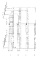
The parallel /
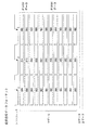
図2に、パラレル/シリアル変換回路6に入力される駆動波形データのフォーマットを示す。これは、データ変換回路5が出力するデータのフォーマットである。図2に示すように、この駆動波形データは、タイミング発生回路4により発生されたタイミング信号の1つであるシフトクロック1に同期し、RGBに対してそれぞれ個別に、2ビットのPHMデータと10ビットのPWMデータとがパラレルに構成されたデータフォーマットである。すなわち、パラレル/シリアル変換回路6に入力される状態においては、赤色の光を
発生する蛍光体に対応する電子放出素子に印加する変調信号を発生させるための階調データは12ビットのパラレルデータ(2ビットの波高値データと10ビットのタイミングデータ)である。他の色についても同様である。すなわち一つの変調信号パルスを形成するためのデータはこの段階では並列数が12、時系列方向のビット数が1のデータフォーマットを有する。ここでは、PHMデータを2ビット、PWMデータを10ビットとした構成の例について説明するが、必ずしもこのような構成に限定されるものではない。
FIG. 2 shows a format of drive waveform data input to the parallel /
また、図3に、パラレル/シリアル変換回路から出力される駆動波形データのフォーマットを示す。図3に示す駆動波形データは、タイミング発生回路4により発生されたタイミング信号の一つであるシフトクロック2に同期し、PHMデータとPWMデータとを、それぞれ個別に、4ビットごとにデータをシリアル化したデータフォーマットである。なお、4ビットに対して不足したデータが存在した場合、すなわちデータ非伝送時間が生じた場合には、不足分を充填するように、疑似データとしてのダミーデータが出力される。後述するように変調回路においてダミーデータは無視できるように構成しているので、ダミーデータとしては任意のデータを使用できる。具体的には、伝送経路に出力する信号レベルを強制的に0レベル(ローレベル)もしくは1レベル(ハイレベル)に規定する構成を好適に採用できる。
FIG. 3 shows the format of drive waveform data output from the parallel / serial conversion circuit. The drive waveform data shown in FIG. 3 is synchronized with the
このシリアル化により、図2に示す12ビットのパラレルデータの並列数12が、並列数4に減少され、時系列方向のビット数は1から4に増えている。具体的には、2ビットのパラレルデータ(並列数が2、時系列方向のビット数が1)であったPHMデータが並列
数が1、時系列方向のビット数が4のフォーマットに変換されている。また、10ビットのパラレルデータ(並列数が10、時系列方向のビット数が1)であったPWMデータが並
列数が3、時系列方向のビット数が4のフォーマットに変換されている。
With this serialization, the
ここで、以下の条件を考える。すなわち、
(1)PHMデータとPWMデータが混在しないようにするという条件、
である。
Here, the following conditions are considered. That is,
(1) The condition that PHM data and PWM data are not mixed,
It is.
この条件を満たす場合、PHMデータのビット数と、PWMデータのビット数によっては、前記使用可能な時間のうちPHMデータを構成するデータビットもしくはPWMデータを構成するデータビットを伝送しない時間が発生する。これがPHMデータのビット数とPWMデータのビット数の不整合によって生じる時間である。 When this condition is satisfied, depending on the number of bits of the PHM data and the number of bits of the PWM data, a time during which the data bits constituting the PHM data or the data bits constituting the PWM data is not transmitted out of the usable time occurs. . This is the time caused by the mismatch between the number of bits of PHM data and the number of bits of PWM data.
またここで示す実施形態では好適な実施の形態として以下の2つの条件を満たすように構成している。すなわち、
(2)一つの伝送経路において、一つの変調信号を形成するためのPHMデータを伝送する時間として使用可能な時間(ここでは4ビットの信号をシリアルに伝送するための時間)と、他の一つの伝送経路において、前記一つの変調信号を形成するためのPWMデータを伝送する時間として使用可能な時間(4ビットの信号をシリアルに伝送するための時間)とを等しくするという条件、
(3)各伝送経路の伝送速度(単位時間あたりに伝送可能なビット数)を同一にするという条件、
である。
Moreover, in embodiment shown here, it is comprised so that the following two conditions may be satisfy | filled as suitable embodiment. That is,
(2) A time that can be used as a time for transmitting PHM data for forming one modulation signal in one transmission path (here, a time for serially transmitting a 4-bit signal), and another one The condition that the time that can be used as the time for transmitting the PWM data for forming the one modulation signal (the time for serially transmitting a 4-bit signal) is made equal in one transmission path,
(3) The condition that the transmission speed of each transmission path (number of bits that can be transmitted per unit time) is the same,
It is.
この2つの条件を採用すると、条件(1)によって生じる、ビット数の不整合に依って生じる前記時間を解消しにくくなる。 Employing these two conditions makes it difficult to eliminate the time caused by the mismatch in the number of bits caused by the condition (1).
この時間に伝送経路の信号レベルが不定になってしまうと誤動作が生じる恐れがある。そこで本実施形態では、該時間に任意のデータ(ダミーデータ)を出力するように構成す
ることでこの問題を解消している。
If the signal level of the transmission path becomes indefinite at this time, a malfunction may occur. Therefore, in this embodiment, this problem is solved by configuring to output arbitrary data (dummy data) at the time.
具体的には、2ビットのPHMデータを4ビットのデータとして出力する構成を採用する
。ここではPHMデータは4つの条件(ここでは変調信号が有するべき最大波高値がどの波
高値になるかを指定する条件)を指定できればよいので、2ビット、すなわち、10進法では、0、1、2、3の値を有する。これを4ビットに変換する。4ビットのデータは10進法では0から15までの任意の値を指定できる。従って、もともとの4つの値0、1、2、3を0から15までの任意の値に変換して送信することができる。ただし、変調回路側で4ビットのデータから特定の2ビットのみを取り出すことで元のPHMデータを再現できるように構成するためには、もとの2ビットのデータ、すなわち、”00”、”01”、”10”、”11”の同じ箇所に、任意のデータビットを挿入するのが好ましい。具体的には、2ビットのデータの前、若しくは後、若しくは途中にデータビットを挿入する構成を採用できる。本実施形態のように複数のデータビットを挿入する場合は、それらの挿入箇所を組み合わせて用いることもできる。例えば、2ビットのデータの前に任意のデータビットとして”00”を挿入すると、上記4つの値は、”0000”、”0001”、”0010”、”0011”となる。この場合、このデータを受信する変調回路では、前半の2つのビットを無視すればよい。挿入されるデータビットは無視することができるので、”00”である必要はなく、他の任意のデータビットを採用できる。また、例えば、2ビットのデータの途中に任意のデータビットとして”1”を挿入し、末尾に任意のデータビットとして”0”を挿入する、という構成も採用できる。この場合、上記4つの値は、”0100”、”0110”、”1100”、”1110”となる。変調回路側では、先頭のビットと3桁目のビットから元の2ビットのPHMデータを再現できる。
Specifically, a configuration is employed in which 2-bit PHM data is output as 4-bit data. Here, the PHM data only needs to be able to specify four conditions (here, the conditions for specifying which peak value the modulation signal should have), so in the case of 2 bits, that is, 0, 1 in the decimal system. Have a value of 2, 3; This is converted to 4 bits. For 4-bit data, an arbitrary value from 0 to 15 can be specified in the decimal system. Therefore, the original four
もともとの4つの値、0、1、2、3(10進法)を、0から15までの任意の値として、7、8、9、10(10進法)に置換して送信することもできる。この場合は4ビットの信号が、”0111”、”1000”、”1001”、”1010”となり、特定の2つのビットを抽出するだけでは元のPHMデータを再現することができない。従って、本
実施形態では、もとのデータのとりうる各値(伝送状態に応じた値。ここではハイレベル、ローレベルの2状態で伝送するので、2進法で表記した値)に対して、同じ位置に任意のビットを付加した値に変換して送信している。信号の伝送状態としては、2値伝送(ハイレベルとローレベルの2つの状態から伝送状態を選択する構成)を好適に採用できるが、他の伝送状態(例えば4つの伝送状態を選択できる構成)も採用できる。すなわち、データビットは0か1に限るものではない。
The original four values, 0, 1, 2, 3 (decimal system) can be replaced with arbitrary values from 0 to 15 and replaced with 7, 8, 9, 10 (decimal system). it can. In this case, the 4-bit signal becomes “0111”, “1000”, “1001”, “1010”, and the original PHM data cannot be reproduced simply by extracting two specific bits. Therefore, in the present embodiment, for each value that can be taken by the original data (value according to the transmission state. Here, since the transmission is performed in two states of high level and low level, a value expressed in binary) , Converted to a value with an arbitrary bit added to the same position and transmitted. As a signal transmission state, binary transmission (a configuration in which a transmission state is selected from two states of a high level and a low level) can be suitably employed, but other transmission states (for example, a configuration in which four transmission states can be selected). Can also be adopted. That is, the data bit is not limited to 0 or 1.
PWMデータも同様である。もともと10ビットのPWMデータを12ビット(一つの伝送経路でシリアルに4ビット伝送する。これを3つの伝送経路で行うので、全部で12ビットのデータとなる)に変換する変換方法としては種々の変換方法を採用可能である。変調回路側で、特定のビットを無視して元の10ビットのPWMデータを再現できるようにするた
めに、本実施形態では、元のPWMデータの全ての値に対して同じ2箇所に任意のビットを
付加して12ビット化するように構成している。
The same applies to PWM data. There are various conversion methods for converting 10-bit PWM data to 12 bits (4 bits are serially transmitted through one transmission path. Since this is performed through three transmission paths, the data becomes 12 bits in total). A conversion method can be adopted. In the present embodiment, in order to allow the modulation circuit side to reproduce the original 10-bit PWM data while ignoring specific bits, in the present embodiment, arbitrary values are provided at the same two locations for all the values of the original PWM data. Bits are added to form 12 bits.
マルチ電源回路7は、複数の電源値を出力可能に構成された電源回路であり、変調回路2を制御するための回路である。マルチ電源回路7は、一般的に電圧源回路であるが、必ずしもこれに限定されるものではない。
The multi
走査電源回路8は、複数の電源値を出力する電源回路であり、走査回路3を制御する回路である。走査電源回路8は、一般的には、電圧源回路であるが、必ずしもこれに限定されるものではない。 The scanning power supply circuit 8 is a power supply circuit that outputs a plurality of power supply values, and is a circuit that controls the scanning circuit 3. The scanning power supply circuit 8 is generally a voltage source circuit, but is not necessarily limited thereto.
次に、変調回路2について説明する。図4に、変調回路2の内部構成を示す。図4に示
すように、変調回路2は、シフトレジスタ9、PWM回路10および出力段回路11を有して構成されている。
Next, the
シフトレジスタ9には、パラレル/シリアル変換回路6によりシリアル変換されたPHMシリアルデータおよびPWMシリアルデータが入力される。また、シフトレジスタ9によりマルチ電子源1の列方向配線に応じた変調データである、PHMパラレルデータおよびPWMパラレルデータが転送される。
The shift register 9 receives PHM serial data and PWM serial data serially converted by the parallel /
PWM回路10には、シフトレジスタ9からマルチ電子源1の列方向配線に応じた変調データであるPHMパラレルデータおよびPWMパラレルデータが入力される。そして、PWM回路10により、出力段回路11が出力する複数の信号レベル(信号の電位であり波高値に相当する)の出力タイミングを指定するための信号が、出力段回路11に対して出力される。
The
また、シフトレジスタ9およびPWM回路10の制御を行うためのタイミング信号が、タイミング発生回路4から入力される。出力段回路11は、マルチ電源回路7に接続され、後述する駆動波形を有した変調信号を出力する回路である。図5に、シフトレジスタ9の内部構成を示し、図6に、図4に示すPWM回路10として列方向配線1本当たりに備わる回路構成の一例を示し、図7に、図4に示す出力段回路11における列方向配線の1本当たりに備わる回路の一例を示す。
A timing signal for controlling the shift register 9 and the
図5に示すように、シフトレジスタ9は、複数の制御回路12および複数の記憶回路13を有して構成される。この第1の実施形態においては、Dフリップフロップ回路、RSフリップフロップ回路およびアンドゲート回路を用いた構成を例に説明するが、制御回路12および記憶回路13は、これに限定されるものではない。
As shown in FIG. 5, the shift register 9 includes a plurality of
図5に示すように、第1の記憶回路13aには、パラレル/シリアル変換回路6でシリアル変換されたPHMシリアルデータが入力される。そして、この第1の記憶回路13aにより、マルチ電子源1の列方向配線に応じた変調データであるPHMパラレルデータが転送される。
As shown in FIG. 5, the PHM serial data serially converted by the parallel /
第2の記憶回路13bには、パラレル/シリアル変換回路6でシリアル変換されたPWMシリアルデータが入力される。なおここで、シリアルデータと称しているが、これはフォーマット変換前のデータに対して、少なくとも一部に対するシリアル化を行って並列数を減らしたデータであることをいうのであって、並列数が1に限るものではない。実際ここで示す形態ではこのPWMシリアルデータは並列数が3である。従って、第2の記憶回路13bもその並列数に合わせて3系統備えることになる。ただし図5では全てを図示することで不明瞭になることを避けるためそれら3系統を集合的に表記している。この第2の記憶回路13bにより、マルチ電子源1の列方向配線に応じた変調データであるPWMパラレルデータが転送される。
PWM serial data serially converted by the parallel /
また、制御回路12には、タイミング発生回路4において発生されたタイミング信号の1つであるシフトスタートパルスとシフトクロックとが入力される。また、制御回路12により、マルチ電子源1の列方向配線に応じた変調データであるPHMシリアルデータおよびPWMデータを第1の記憶回路13aおよび第2の記憶回路13bに記録するための制御信号が発生される。
The
この制御回路12が発生した記録制御信号に応じて、PHMシリアルデータが第1の記憶回路13aに記録されるとともに、PWMシリアルデータが第2の記憶回路13bに記録される。
In accordance with the recording control signal generated by the
第1の記憶回路13aおよび第2の記憶回路13bから出力されるデータは、パラレルに構成されており、マルチ電子源1の列方向配線に応じて、一括してPWM回路10に出力される。
The data output from the
具体的には、4ビットの時系列方向のPWMシリアルデータが図5に示す第2の記憶回路13bの4つのフリップフロップで順次に転送される。該4ビットの時系列方向のPWMシリアルデータが4つのフリップフロップに記憶された状態において、出力タイミングがフリップフロップに対して指定されることで4ビットのパラレルデータが出力される。これを3系統夫々で並列に行うことによって、12ビットのPWMパラレルデータが出力される。ただし、2ビットはダミーデータなので、該ダミーデータは無視され、実際には10ビットのPWMパラレルデータが出力される。
Specifically, 4-bit PWM serial data in the time series direction is sequentially transferred by the four flip-flops of the
また、4ビットの時系列方向のPHMシリアルデータが第1の記憶回路13aに入力される。ただし4ビットのうちの2ビットはダミーデータであるので、記憶回路13aはダミーデータを除く2ビットを記憶できるように2つのフリップフロップで構成されている。これによってPHMシリアルデータはパラレル化される。
Further, 4-bit PHM serial data in the time series direction is input to the
次に、図6を用いて、PWM回路10について説明する。なお、図6に示すPWM回路10は、あくまで一例であり、必ずしもこの回路構成に限定されるものではない。
Next, the
ここで示す実施形態のように、変調信号の振幅方向の制御と時間幅方向の制御との両方を行って変調信号を発生させる構成においては、種々の複雑な変調信号波形を発生させることができる。例えば、変調信号のパルス全体の時間幅の単位時間(クロック信号をカウントすることで時間幅を設定する構成においてはカウントの対象となるクロック信号の一周期がこれに相当する。)毎に個別に波高値制御すべく波高値データを各単位時間に対応させて発生させる構成も採用できる。しかしこのような複雑な構成をとる必要はない。具体的には、波高値データであるPHMデータとしては、一つの変調信号の波形のうちの少なくとも一点の波高値を要求される明るさに対応して規定できる情報を含んでいればよい。具体的には、少なくとも一点の波高値を規定する情報としては、変調信号における最大波高値を特定する情報を好適に採用できる。なお波高値の大小は電位の大小とは限らない。例えば走査信号の選択電位が変調信号のオン状態に対応する電位よりも高い電位である場合は、変調信号の波高値は、電位が低い方が大きいことになる。 In the configuration in which the modulation signal is generated by performing both the amplitude direction control and the time width direction control of the modulation signal as in the embodiment shown here, various complex modulation signal waveforms can be generated. . For example, each unit time of the time width of the entire pulse of the modulation signal (in the configuration in which the time width is set by counting the clock signal, one period of the clock signal to be counted corresponds to this) individually. A configuration for generating peak value data corresponding to each unit time for peak value control can also be adopted. However, it is not necessary to take such a complicated configuration. Specifically, the PHM data that is the peak value data only needs to include information that can define the peak value of at least one point of the waveform of one modulation signal in accordance with the required brightness. Specifically, as information defining the peak value of at least one point, information for specifying the maximum peak value in the modulated signal can be suitably employed. Note that the magnitude of the peak value is not necessarily the magnitude of the potential. For example, when the selection potential of the scanning signal is higher than the potential corresponding to the ON state of the modulation signal, the peak value of the modulation signal is larger when the potential is lower.
またタイミングデータであるPWMデータとしては、例えば、変調信号の波形の各波高値の部分夫々の遷移タイミング(ある波高値に制御されている状態から他の波高値に遷移するための制御を開始するタイミング)を規定する情報を全て含む構成にすることもできる。しかしこのような複雑な構成をとる必要はない。具体的には、タイミングデータであるPWMデータとしては、変調信号の信号レベルを他のレベルに遷移させるタイミングを、要求される明るさに対応して少なくとも1箇所規定できる情報を含んでいればよい。具体的には、ある変調信号において、その変調信号が使用する波高値のうちの最大の波高値からより小さい波高値に遷移させるタイミングを規定できるデータをタイミングデータとして用いる構成を好適に採用できる。なおデータに基づくタイミングの規定の方法は種々のものを採用できる。基準時点からの経過時間を計時する構成を採用し、タイミングデータがその計時時間を直接若しくは間接的に指定する構成を好適に採用できる。具体的には計時はクロックのカウントによって行う構成を好適に採用できる。この場合計時時間の指定はカウント数を直接若しくは間接的に指定することで行うことができる。 As PWM data that is timing data, for example, the transition timing of each peak value portion of the waveform of the modulation signal (control for shifting from a state controlled to a certain peak value to another peak value is started. It is also possible to adopt a configuration that includes all information that defines (timing). However, it is not necessary to take such a complicated configuration. Specifically, the PWM data that is the timing data only needs to include information that can define the timing at which the signal level of the modulation signal is shifted to another level in accordance with the required brightness. . Specifically, it is possible to suitably employ a configuration that uses, as timing data, data that can define the timing of transition from the maximum peak value used by the modulation signal to a smaller peak value in a certain modulation signal. Note that various methods for defining timing based on data can be adopted. A configuration in which the elapsed time from the reference time is measured and a configuration in which the timing data directly or indirectly specifies the measured time can be suitably employed. Specifically, it is possible to suitably employ a configuration in which clocking is performed by clock counting. In this case, the time measurement time can be specified by specifying the count number directly or indirectly.
この第1の実施形態によるPWM回路10は、ラッチ回路として、PWMパラレルデータ用ラッチ回路14およびPHMパラレルデータ用ラッチ回路15を有している。また、
このPWM回路10には、カウンタ関連の回路として、カウンタ回路16およびカウンタクリア信号発生回路17が設けられている。なお、この第1の実施形態においては、カウンタクリア信号発生回路17をDフリップフロップ回路とXOR回路とを用いて構成しているが、この回路構成は、あくまでも一例であり、必ずしもこの回路構成に限定されるものではない。
The
The
また、PWM回路10は、デコード回路として、PHMデータデコード回路18および初期データセット信号デコード回路19が設けられ、記憶回路として、V1スタートデータ記憶回路20、V2スタートデータ記憶回路21、V3スタートデータ記憶回路22、V4スタートデータ記憶回路23、V1エンドデータ記憶回路24、V2エンドデータ記憶回路25、V3エンドデータ記憶回路26、およびV4エンドデータ記憶回路27が設けられている。
The
また、PWM回路10は、エンドデータ選択回路として、V1エンドデータ選択回路28、V2エンドデータ選択回路29、V3エンドデータ選択回路30、およびV4エンドデータ選択回路31を有し、データ比較回路として、V1スタートデータ比較器32、V2スタートデータ比較器33、V3スタートデータ比較器34、V4スタートデータ比較器35、V1エンドデータ比較器36、V2エンドデータ比較器37、V3エンドデータ比較器38およびV4エンドデータ比較器39を有している。
The
また、PWM回路10は、パルス幅発生回路として、V1パルス幅発生回路40、V2パルス幅発生回路41、V3パルス幅発生回路42およびV4パルス幅発生回路43を有している。
Further, the
次に、以上のように構成されたこの第1の実施形態によるPWM回路10について説明する。
Next, the
まず、PWMパラレルデータ用ラッチ回路14は、シフトレジスタ9内の第2の記憶回路13bに記録されたマルチ電子源1の列方向配線に応じた変調データであるPWMパラレルデータを、タイミング発生回路4により発生されたタイミング信号の一つであるロード信号のタイミングに応じてラッチするための回路である。
First, the PWM parallel
また、PHMパラレルデータ用ラッチ回路15は、シフトレジスタ9内の第1の記憶回路13aに記録されたマルチ電子源1の列方向配線に応じた変調データであるPHMパラレルデータを、タイミング発生回路4により発生されたタイミング信号の一つであるロード信号のタイミングに応じてラッチするための回路である。
In addition, the PHM parallel
また、カウンタ回路16は、タイミング発生回路4により発生されたタイミング信号の一つであるPWMクロックと、カウンタクリア信号発生回路17により発生されたカウンタクリア信号とに基づいて、内部タイミングを規定するカウントデータを、V1スタートデータ比較器32、V1スタートデータ比較器32、V2スタートデータ比較器33、V3スタートデータ比較器34、V4スタートデータ比較器35、V1エンドデータ比較器36、V2エンドデータ比較器37、V3エンドデータ比較器38およびV4エンドデータ比較器39に出力するための回路である。
The
また、カウンタクリア信号発生回路17は、タイミング発生回路4により発生されたタイミング信号の一つであるロード信号とPWMクロックとから、内部タイミングを規定するカウンタのクリア信号を発生するための回路である。
The counter clear signal generation circuit 17 is a circuit for generating a counter clear signal for defining internal timing from a load signal which is one of timing signals generated by the
PHMデータデコード回路18は、PHMパラレルデータ用ラッチ回路15によってラ
ッチされたPHMパラレルデータに応じて、V1エンドデータ選択回路28、V2エンドデータ選択回路29およびV3エンドデータ選択回路30の選択信号を発生するデコード回路である。
The PHM data decode
この第1の実施形態においては、2ビットのPHMパラレルデータに応じて4つの選択信号が発生される。すなわち、PHMデータ=”00”の場合には、V1エンドデータ選択回路28の選択信号に”1”が入力され、そのほかの選択回路の選択信号は”0”となる。ここで、”00”は、バイナリ表示の数値を示す。また、PHMデータ=”01”の場合は、V2エンドデータ選択回路29の選択信号に”1”が入力され、他の選択回路の選択信号は、”0”となる。また、PHMデータ=”10”の場合はV3エンドデータ選択回路30の選択信号に”1”が入力され、他の選択回路の選択信号は”0”となる。PHMデータ=”11”の場合はV4エンドデータ選択回路31の選択信号に”1”が入力され、他の選択回路の選択信号は”0”となる。
In the first embodiment, four selection signals are generated according to 2-bit PHM parallel data. That is, when PHM data = “00”, “1” is input to the selection signal of the V1 end
また、PWM回路10における初期データセット信号デコード回路19は、タイミング発生回路4において発生されたタイミング信号の一つである初期データセット信号に応じて、V1スタートデータ記憶回路20、V2スタートデータ記憶回路21、V3スタートデータ記憶回路22、V4スタートデータ記憶回路23、V1エンドデータ記憶回路24、V2エンドデータ記憶回路25、V3エンドデータ記憶回路26およびV4エンドデータ記憶回路27に、PWMパラレルデータ用ラッチ回路14によってラッチされたPWMデータを記録するための書込み信号を発生するデコード回路である。
Further, the initial data set signal decoding circuit 19 in the
この第1の実施形態においては、3ビットの初期データセット信号に応じて8本の選択信号が発生される。 In the first embodiment, eight selection signals are generated according to a 3-bit initial data set signal.
すなわち、初期データセット信号=”000”の場合、V1スタートデータ記憶回路20の書込信号だけがオンになり、PWMパラレルデータ用ラッチ回路14によりラッチされたV1への波高値遷移(波高値を大きくする方向の遷移)を開始する位置を指定するデータ(V1スタートデータ:これはPWMデータと同じ経路で予め与えら得るタイミング指定用データである)が、V1スタートデータ記憶回路20に記録される。
That is, when the initial data set signal = “000”, only the write signal of the V1 start
初期データセット信号=”001”の場合、V2スタートデータ記憶回路21の書込信号だけがオンになり、PWMパラレルデータ用ラッチ回路14によりラッチされたV2への波高値遷移(波高値を大きくする方向の遷移)を開始する位置を指定するデータ(V2スタートデータ:これはPWMデータと同じ経路で予め与えられるタイミング指定用データである)が、V2スタートデータ記憶回路21に記録される。
When the initial data set signal = “001”, only the write signal of the V2 start
初期データセット信号=”010”の場合、V3スタートデータ記憶回路22の書込信号だけがオンになり、PWMパラレルデータ用ラッチ回路14によりラッチされたV3への波高値遷移(波高値を大きくする方向の遷移)を開始する位置を指定するデータ(V3スタートデータ:これはPWMデータと同じ経路で予め与えられるタイミング指定用データである)がV3スタートデータ記憶回路22に記録される。
When the initial data set signal = “010”, only the write signal of the V3 start
初期データセット信号=”011”の場合、V4スタートデータ記憶回路23の書込信号だけがオンになり、PWMパラレルデータ用ラッチ回路14によりラッチされたV4への波高値遷移(波高値を大きくする方向の遷移)を開始する位置を指定するデータ(V4スタートデータ:これはPWMデータと同じ経路で予め与えられるタイミング指定用データである)がV4スタートデータ記憶回路23に記録される。
When the initial data set signal = “011”, only the write signal of the V4 start
初期データセット信号=”100”の場合、V1エンドデータ記憶回路24の書込信号
だけがオンになり、PWMパラレルデータ用ラッチ回路14によりラッチされたV1からより低い波高値への遷移を開始する位置を指定するデータ(V1エンドデータ:これはPWMデータと同じ経路で予め与えられるタイミング指定用データである)がV1エンドデータ記憶回路24に記録される。
When the initial data set signal = "100", only the write signal of the V1 end
初期データセット信号=”101”の場合、V2エンドデータ記憶回路25の書込信号だけがオンになり、PWMパラレルデータ用ラッチ回路14によりラッチされたV2からより低い波高値への遷移を開始する位置を指定するデータ(V2エンドデータ:これはPWMデータと同じ経路で予め与えられるタイミング指定用データである)がV2エンドデータ記憶回路25に記録される。
When the initial data set signal = “101”, only the write signal of the V2 end
初期データセット信号=”110”の場合、V3エンドデータ記憶回路26の書込信号だけがオンになり、PWMパラレルデータ用ラッチ回路14によりラッチされたV3からより低い波高値への遷移を開始する位置を指定するデータ(V3エンドデータ:これはPWMデータと同じ経路で予め与えられるタイミング指定用データである)がV3エンドデータ記憶回路26に記録される。
When the initial data set signal = “110”, only the write signal of the V3 end
初期データセット信号=”111”の場合、V4エンドデータ記憶回路27の書込信号だけがオンになり、PWMパラレルデータ用ラッチ回路14によりラッチされたV4からより低い波高値への遷移を開始する位置を指定するデータ(V4エンドデータ:これはPWMデータと同じ経路で予め与えられるタイミング指定用データである)がV4エンドデータ記憶回路27に記録される。
When the initial data set signal = “111”, only the write signal of the V4 end
これらのスタート位置指定データ及びエンド位置指定データが記録されるデータ記憶回路20〜27に、装置起動時を含む画像非表示期間中に、駆動波形を形成するための上述のパラメータ(V1スタートデータ、V2スタートデータ、V3スタートデータ、V4スタートデータ、V1エンドデータ、V2エンドデータ、V3エンドデータおよびV4エンドデータ)が順次転送される。これにより、データ記憶回路20〜27に、パラメータ(V1スタートデータ、V2スタートデータ、V3スタートデータ、V4スタートデータ、V1エンドデータ、V2エンドデータ、V3エンドデータおよびV4エンドデータ)が記録される。
In the
また、PWM回路10におけるV1エンドデータ選択回路28は、PWMパラレルデータ用ラッチ回路14によりラッチされたPWMデータとV1エンドデータ記憶回路24に記録されたV1エンドデータとのいずれかを選択する選択回路である。この選択は、PHMデータデコード回路18から出力されるPHMデータに応じた選択信号により実行される。
The V1 end
また、V2エンドデータ選択回路29は、PHMデータデコード回路18から出力されるPHMデータに応じた選択信号により、PWMパラレルデータ用ラッチ回路14によりラッチされたPWMデータと、V2エンドデータ記憶回路25に記録されたV2エンドデータとのいずれかを選択する選択回路である。
Further, the V2 end
同様に、V3エンドデータ選択回路30は、PHMデータデコード回路18から出力されるPHMデータに応じた選択信号により、PWMパラレルデータ用ラッチ回路14によってラッチされたPWMデータとV3エンドデータ記憶回路26に記録されたV3エンドデータとのいずれかを選択する選択回路である。
Similarly, the V3 end
また、同様に、V4エンドデータ選択回路31は、PHMデータデコード回路18から出力されるPHMデータに応じた選択信号により、PWMパラレルデータ用ラッチ回路1
4によりラッチされたPWMデータとV4エンドデータ記憶回路26に記録されたV4エンドデータとのいずれかを選択する選択回路である。
Similarly, the V4 end
4 is a selection circuit that selects either the PWM data latched by 4 or the V4 end data recorded in the V4 end
V1からV4エンドデータ選択回路は、選択信号が”1”の場合に、PWMデータを選択し、選択信号が”0”の場合に、対応するエンドデータ記憶回路に記憶されたエンドデータを選択する。 The V1 to V4 end data selection circuit selects the PWM data when the selection signal is “1”, and selects the end data stored in the corresponding end data storage circuit when the selection signal is “0”. .
また、V1スタートデータ比較器32は、V1スタートデータ記憶回路20に記録されたV1スタートデータと、内部タイミングを規定するカウンタ回路16のカウントデータとが一致したときに、V1スタートパルスを発生するための比較器である。V2スタートデータ比較器33は、V2スタートデータ記憶回路21に記録されたV2スタートデータと、カウンタ回路16のカウントデータとが一致したときに、V2スタートパルスを発生するための比較器である。V3スタートデータ比較器34は、V3スタートデータ記憶回路22に記録されたV3スタートデータと、カウンタ回路16のカウントデータとが一致したときに、V3スタートパルスを発生する比較器である。V4スタートデータ比較器35は、V4スタートデータ記憶回路23に記録されたV4スタートデータと、カウンタ回路16のカウントデータとが一致したときに、V4スタートパルスを発生する比較器である。
The V1 start
また、V1エンドデータ比較器36は、V1エンドデータ選択回路28により選択されたV1エンドデータまたはPWMデータと、カウンタ回路16のカウントデータとが一致したときに、V1エンドパルスを発生する比較器である。V2エンドデータ比較器37は、V2エンドデータ選択回路29により選択されたV2エンドデータもしくはPWMデータと、カウンタ回路16のカウントデータとが一致したときに、V2エンドパルスを発生する比較器である。V3エンドデータ比較器38は、V3エンドデータ選択回路30により選択されたV3エンドデータまたはPWMデータと、カウンタ回路16のカウントデータとが一致したときに、V3エンドパルスを発生する比較器である。V4エンドデータ比較器39は、V4エンドデータ選択回路31により選択されたV4エンドデータまたはPWMデータと、カウンタ回路16のカウントデータとが一致したときに、V4エンドパルスを発生する比較器である。
The V1
また、V1パルス幅発生回路40は、パルス幅波形TV1を出力するPWM回路である。パルス幅波形TV1は、V1スタートデータ比較器32において発生されたV1スタートパルスで立ち上がり、V1エンドデータ比較器36において発生されたV1エンドパルスで立ち下がる波形である。
The V1 pulse
また、V2パルス幅発生回路41は、パルス幅波形TV2を出力するPWM回路である。パルス幅波形TV2は、V2スタートデータ比較器33において発生されたV2スタートパルスで立ち上がり、V2エンドデータ比較器37において発生されたV2エンドパルスで立ち下がる波形である。
The V2 pulse
また、V3パルス幅発生回路42は、パルス幅波形TV3を出力するPWM回路である。このパルス幅波形TV3は、V3スタートデータ比較器34において発生されたV3スタートパルスで立ち上がり、V3エンドデータ比較器38において発生されたV3エンドパルスで立ち下がる波形である。
The V3 pulse
また、V4パルス幅発生回路43は、パルス幅波形TV4を出力するPWM回路である。このパルス幅波形TV4は、V4スタートデータ比較器35において発生されたV4スタートパルスで立ち上がり、V4エンドデータ比較器39において発生されたV4エンドパルスで立ち下がるパルス幅波形である。
The V4 pulse
なお、この第1の実施形態においては、PWM回路として、RSフリップフロップ回路における、セット入力にスタートパルスを入力し、リセット入力にエンドパルスを入力する回路を採用しているが、必ずしもこのような構成に限定されるものではない。 In the first embodiment, as the PWM circuit, a circuit that inputs a start pulse to a set input and an end pulse to a reset input in an RS flip-flop circuit is employed. The configuration is not limited.
また、図7に示すように、電位V1〜V4は、0<V1<V2<V3<V4であり、それぞれPWM出力波形TV1、TV2、TV3およびTV4に対応して出力される。また、トランジスタQ1、Q2、Q3およびQ4は、オンすることによりそれぞれ電位V1〜V4を出力端子OUTPUTに出力可能に構成されている。なお、トランジスタQ1〜Q4については、ペアトランジスタにより構成することも可能である。 As shown in FIG. 7, the potentials V1 to V4 are 0 <V1 <V2 <V3 <V4, and are output corresponding to the PWM output waveforms TV1, TV2, TV3, and TV4, respectively. The transistors Q1, Q2, Q3, and Q4 are configured to output potentials V1 to V4 to the output terminal OUTPUT when turned on. Note that the transistors Q1 to Q4 can be configured by pair transistors.
次に、以上のように構成された変調回路2の出力端子OUTPUTから出力される駆動波形について、図8を参照しつつ説明する。
Next, driving waveforms output from the output terminal OUTPUT of the
図8Aに、PHMデータ=”11”の場合において、電位V1〜V4を用いた駆動波形を示す。図8Aに示すように、電位V1の立ち上がり位置については、V1スタートデータ記憶回路20に記憶されたV1スタートデータにより規定される。また、電位V2の立ち上がり位置は、V2スタートデータ記憶回路21に記憶されたV2スタートデータにより規定される。また、電位V3の立ち上がり位置は、V3スタートデータ記憶回路22に記憶されたV3スタートデータにより規定され、電位V4の立ち上がり位置がV4スタートデータ記憶回路23に記憶されたV4スタートデータにより規定される。
FIG. 8A shows a driving waveform using the potentials V1 to V4 when PHM data = “11”. As shown in FIG. 8A, the rising position of the potential V1 is defined by the V1 start data stored in the V1 start
他方、電位V1の立ち下がり位置については、V1エンドデータ記憶回路24に記憶されたV1エンドデータにより規定され、電位V2の立ち下がり位置がV2エンドデータ記憶回路25に記憶されたV2エンドデータにより規定され、電位V3の立ち下がり位置はV3エンドデータ記憶回路26に記憶されたV3エンドデータにより規定され、電位V4の立ち下がり位置はPWMデータにより規定される。
On the other hand, the falling position of the potential V1 is defined by the V1 end data stored in the V1 end
図8Bに、PHMデータ=”10”の場合において、電位V1〜V3まで使用した駆動波形を示す。 FIG. 8B shows drive waveforms used for potentials V1 to V3 when PHM data = “10”.
図8Bに示すように、電位V1の立ち上がり位置はV1スタートデータ記憶回路20に記憶されたV1スタートデータにより規定され、電位V2の立ち上がり位置は、V2スタートデータ記憶回路21に記憶されたV2スタートデータにより規定され、電位V3の立ち上がり位置は、V3スタートデータ記憶回路22に記憶されたV3スタートデータにより規定される。
As shown in FIG. 8B, the rising position of the potential V1 is defined by the V1 start data stored in the V1 start
他方、電位V1の立ち下がり位置は、V1エンドデータ記憶回路24に記憶されたV1エンドデータにより規定され、電位V2の立ち下がり位置は、V2エンドデータ記憶回路25に記憶されたV2エンドデータにより規定され、電位V3の立ち下がり位置は、PWMデータにより規定される。
On the other hand, the falling position of the potential V1 is defined by the V1 end data stored in the V1 end
また、図8Cに、PHMデータ=”01”の場合において、電位V1とV2を使用した駆動波形を示す。 FIG. 8C shows a driving waveform using the potentials V1 and V2 when PHM data = “01”.
図8Cに示すように、電位V1の立ち上がり位置は、V1スタートデータ記憶回路20に記憶されたV1スタートデータにより規定され、電位V2の立ち上がり位置は、V2スタートデータ記憶回路21に記憶されたV2スタートデータにより規定され、電位V1の立ち下がり位置は、V1エンドデータ記憶回路24に記憶されたV1エンドデータにより規定され、電位V2の立ち下がり位置は、PWMデータにより規定される。
As shown in FIG. 8C, the rising position of the potential V1 is defined by the V1 start data stored in the V1 start
図8Dに、PHMデータ=”01”の場合において、電位V1を使用した駆動波形を示す。図8Dに示すように、電位V1の立ち上がり位置は、V1スタートデータ記憶回路20に記憶されたV1スタートデータにより規定され、電位V1の立ち下がり位置は、PWMデータにより規定される。
FIG. 8D shows a drive waveform using the potential V1 when PHM data = “01”. As shown in FIG. 8D, the rising position of the potential V1 is defined by the V1 start data stored in the V1 start
以上から明らかなように、本実施形態においては、各階調データに対応する変調信号は、それぞれの最大波高値に制御される部分のパルス幅が階調データを構成するタイミングデータ(PWMデータ)で決まる(変調される)ことになる。各変調信号のその他の部分(最大波高値に制御される部分以外の部分)の形状は、V1スタートデータ、V2スタートデータ、V3スタートデータ、V4スタートデータ、V3エンドデータ、V2エンドデータ、V1エンドデータによって階調データに依らずに決定することができる。ただし、変調信号のどの部分のパルス幅を階調データに対応づけて決定するかは、この構成に限るものではない。本実施形態では、2番目以降の波高値(前記V2、V3、V4に相当)を用いる変調信号においては、変調信号の立ち上がりの部分と立ち下がりの部分において、波高値が基準レベルから直接その変調信号における最大波高値まで立ち上がらないように途中の波高値を経由させている。これによって変調信号の印加によって生じるリンギングが抑制できる。具体的には変調信号の立ち上がり部分と立ち下がり部分が階段形状になるように構成しており、これは、V1スタートデータ、V2スタートデータ、V3スタートデータ、V4スタートデータ、V3エンドデータ、V2エンドデータ、V1エンドデータを階段形状が得られるタイミングに設定することで実現している。 As is apparent from the above, in this embodiment, the modulation signal corresponding to each gradation data is the timing data (PWM data) in which the pulse width of the portion controlled to the maximum peak value constitutes the gradation data. It will be determined (modulated). The shape of the other part of each modulation signal (the part other than the part controlled to the maximum peak value) is V1 start data, V2 start data, V3 start data, V4 start data, V3 end data, V2 end data, V1 end. The data can be determined without depending on the gradation data. However, it is not limited to this configuration which part of the modulation signal the pulse width is determined in association with the gradation data. In the present embodiment, in the modulation signal using the second and subsequent peak values (corresponding to V2, V3, and V4), the peak value is directly modulated from the reference level at the rising and falling portions of the modulation signal. In order not to rise to the maximum peak value in the signal, the peak value on the way is routed. Thereby, ringing caused by application of the modulation signal can be suppressed. More specifically, the rising and falling portions of the modulation signal are configured to have a staircase shape, which is V1 start data, V2 start data, V3 start data, V4 start data, V3 end data, and V2 end. This is realized by setting the data and V1 end data at a timing at which a staircase shape can be obtained.
以上説明したように、この第1の実施形態による表示素子の駆動回路によれば、PWMデータとPHMデータとを、それぞれを構成するデータビットのビット数より少ない伝送経路(伝送線)により変調回路2に伝送するようにシリアル化していることにより、振幅変調とパルス幅変調とを併用した変調を行うための異なる属性を有する2種類のデータを、構成において伝送線数を大幅に増やすことなく伝送することが可能となる。 As described above, according to the display element driving circuit according to the first embodiment, the PWM data and the PHM data are modulated by the transmission path (transmission line) having a smaller number of data bits than each other. 2 types of data having different attributes for performing modulation using both amplitude modulation and pulse width modulation can be transmitted without significantly increasing the number of transmission lines in the configuration. It becomes possible to do.
特にこの実施形態においては、パラレル/シリアル変換回路から変調回路に階調データを伝送する伝送経路のいずれにおいても、属性の異なるデータである波高値データとタイミングデータとを混在させないようにしている。そのため、パラレル/シリアル変換回路から変調回路に階調データを伝送した後で、波高値データとタイミングデータとを分離するための構成を設けなくてもよいというメリットがある。 Particularly in this embodiment, the peak value data and the timing data which are data having different attributes are not mixed in any of the transmission paths for transmitting the gradation data from the parallel / serial conversion circuit to the modulation circuit. Therefore, there is an advantage that it is not necessary to provide a configuration for separating the peak value data and the timing data after the grayscale data is transmitted from the parallel / serial conversion circuit to the modulation circuit.
(第2の実施形態)
次に、この発明の第2の実施形態について説明する。なお、この第2の実施形態による駆動回路の概略は、第1の実施形態におけると同様である。すなわち、図1に示すように、この第2の実施形態による駆動装置は、変調回路2、走査回路3、タイミング発生回路4、データ変換回路5、パラレル/シリアル変換回路6、マルチ電源回路7および走査電源回路8を有して構成され、マルチ電子源1を駆動する回路である。
(Second Embodiment)
Next explained is the second embodiment of the invention. The outline of the drive circuit according to the second embodiment is the same as that in the first embodiment. That is, as shown in FIG. 1, the driving apparatus according to the second embodiment includes a
また、走査回路3は、マルチ電子源1の行方向配線に接続され、変調回路2の出力をマルチ電子源1のいずれの行に信号を供給するかを選択するための回路である。そして、一般的には、一行ずつ順次行選択するようにした線順次走査が実行されるが、必ずしも線順次走査に限定されるものではなく、飛び越し走査や、複数行を同時に選択したり、面状に選択したりすることも可能である。すなわち、走査回路3は、マルチ電子源1に含まれる複数電子源のうちの駆動対象となる複数の電子源が接続される行方向配線に対して所定時間選択電位を供給し、その他の時間に非選択電位を供給することにより、行選択を行う選択手段である。なお、以下に説明する変調回路2およびこの変調回路2にシリアルデータの供給する周辺回路以外の回路構成については、第1の実施形態におけると同様であるの
で、その説明を省略する。
The scanning circuit 3 is connected to the row direction wiring of the
次に、この発明の第2の実施形態による変調回路2およびシリアルデータの供給について説明する。図9に、変調回路2の内部構成および、変調回路2にシリアルデータを供給する周辺回路を示す。図9に示すように、この第2の実施形態による変調回路2は、第1の実施形態におけると同様に、シフトレジスタ9、PWM回路10および出力段回路11を有して構成されている。なお、出力段回路11は、マルチ電源回路7に接続され、後述する駆動波形を有する変調信号を出力するための回路である。
Next explained is the
データ変換回路5は、外部からマルチ電子源1の輝度階調制御する輝度階調データを変調回路2に適した駆動波形データフォーマットにデータ変換を行うための回路である。
The
パラレル/シリアル変換回路6は、データ変換回路5から供給された輝度階調データを、PHMデータおよびPWMデータのいずれのデータの属性に関わらず、一律のパラレルデータとして取り扱い、そのパラレルデータをシリアル差動データに変換する回路である。この第2の実施形態においては、差動データの場合を例にして説明するが、必ずしも差動データに限定されるものではなく、具体的に、例えば、シングルエンドデータや擬似差動データなどを利用することも可能である。
The parallel /
次に、図2および図10を用いて、パラレル/シリアル変換回路6に入力されるデータフォーマット、およびパラレル/シリアル変換回路6から出力されるデータフォーマットについて説明をする。なお、パラレル/シリアル変換回路に入力される駆動波形データのフォーマットは、第1の実施形態におけると同様であるので、説明を省略する。図10に、本実施形態のパラレル/シリアル変換回路から出力される駆動波形データのフォーマットを示す。
Next, the data format input to the parallel /
すなわち、図2に示すように、第2の実施形態による駆動波形データは、第1の実施形態におけると同様に、RGBでそれぞれ個別に、2ビットのPHMデータと10ビットのPWMデータとがパラレルに構成されたデータフォーマットである。そして、この駆動波形データは、タイミング発生回路4からデータ変換回路5に供給されるタイミング信号の1つであるシフトクロック1に同期されている。なお、この第2の実施形態においては、PHMデータを2ビット、PWMデータを10ビットとした場合を例に説明するが、必ずしも10ビットに限定されるものではなく、それ以外のビット数を採用することも可能である。
That is, as shown in FIG. 2, the drive waveform data according to the second embodiment is obtained by converting 2-bit PHM data and 10-bit PWM data in parallel separately for RGB, as in the first embodiment. The data format is configured as follows. The drive waveform data is synchronized with a
図10に示すように、この第2の実施形態によるシリアルデータは、タイミング発生回路4から発生されたタイミング信号の1つであるシフトクロック2に同期されて、PHMデータおよびPWMデータのいずれであるかというデータの属性とは無関係に、一律のデータとして4ビットごとにデータをシリアル化したデータフォーマットである。なお、この第2の実施形態においては、シフトクロックの立ち上がりと立ち下がりとの両エッジにおいて、トリガをかける構成を採用しているが、必ずしも、このような構成に限定されるものではない。さらに、この第2の実施形態においては、データビット数が4の倍数となる値(4で割り切れる値)としているが、データビット数が4で割り切れない場合、すなわち、データ非伝送時間が生じる場合には、4ビットに足りないデータに、疑似データとしてのダミーデータが充填されて出力される。
As shown in FIG. 10, the serial data according to the second embodiment is either PHM data or PWM data in synchronization with a
また、図9に示すように、変調回路2は、マルチ電子源1の列方向配線に接続されている。この変調回路2は、パラレル/シリアル変換回路6によってPHMデータとPWMデータとが一律にシリアル変換された変調データ(階調データ)に応じて、マルチ電子源1に変調信号を供給するための回路である。すなわち、この変調回路2は、パラレル/シリアル変換回路6から入力された変調データに基づいて、変調された変調信号を複数の電子源にそれぞれ接続する列方向配線に与える変調手段として機能する。
As shown in FIG. 9, the
次に、この第2の実施形態による変調回路2に設けられるシフトレジスタ9について説明する。図11に、この第2の実施形態によるシフトレジスタ9の内部構成を示す。
Next, the shift register 9 provided in the
図11に示すように、この第2の実施形態によるシフトレジスタ9には、パラレル/シリアル変換回路6によってシリアル変換されたPHMシリアルデータおよびPWMシリアルデータが入力される。また、シフトレジスタ9からは、マルチ電子源1の列方向配線に応じた変調データであるPHMパラレルデータおよびPWMパラレルデータが出力される。図10に示すように、一つの表示素子を1つの選択期間の間変調するための変調信号を発生するのに用いるデータは、パラレル/シリアル変換回路6に並列数12のパラレルデータとして入力され、並列数3、時系列方向のビット数4のフォーマットにシリアル変換される。すなわち図11に示すシフトレジスタ9には3系統(並列数3)の信号がシリアルデータとして入力されている。
As shown in FIG. 11, the PHM serial data and PWM serial data serially converted by the parallel /
シフトレジスタ9から出力された変調データとしてのPHMパラレルデータおよびPWMパラレルデータは、PWM回路10に供給される。このPWM回路10は、出力段回路11において、それぞれの出力電圧に応じた出力を発生させるための回路である。また、タイミング発生回路4からは、シフトレジスタ9およびPWM回路10を制御するためのタイミング信号が供給される。
The PHM parallel data and PWM parallel data as modulation data output from the shift register 9 are supplied to the
また、図11に示すように、この第2の実施形態によるシフトレジスタ9は、複数の制御回路52および複数の記憶回路53を有して構成される。なお、この第2の実施形態においては、制御回路52および記憶回路53を、Dフリップフロップ回路、RSフリップフロップ回路およびオアゲート回路を用いて構成する場合を例として説明するが、必ずしもこのような回路構成に限定されるものではない。
As shown in FIG. 11, the shift register 9 according to the second embodiment includes a plurality of
記憶回路53a、記憶回路53b、記憶回路53c、はそれぞれシリアル化された3系統のデータをパラレルデータに変換する回路を構成する。記憶回路53b、記憶回路53cには、PHMデータとPWMデータが混在しない2系統のシリアルデータがそれぞれ入力される。シリアルデータは記憶素子であるフリップフロップで転送され、所定のタイミングでパラレルデータとして出力される。記憶回路53aには、パラレル/シリアル変換回路6で一律にシリアル変換されたPHMデータおよびPWMデータを内包したシリアルデータの中で、特にPHMデータとPWMデータとがシリアルに混在されたデータが入力される。記憶回路53aでは記憶素子であるフリップフロップが4つ直列に接続されている。各フリップフロップは入力されるデータビットを記憶すると共に、次段のフリップフロップに記憶していたデータビットを入力する。この4つのフリップフロップによって4ビットのシリアルデータを保持する。そのうちの2ビットのデータをPHMデータとして出力し、他の2ビットをPWMデータとして出力する。記憶回路53aが出力する2ビットのPWMデータは、記憶回路53bが出力する4ビットのPWMデータ、及び記憶回路53cが出力する4ビットのPWMデータと共に10ビットのPWMパラレルデータを構成するデータとなる。これによってマルチ電子源1の列方向配線に応じた変調データであるPHMパラレルデータとPWMパラレルデータとがPWM回路10に出力される。
Each of the
また、制御回路52には、タイミング発生回路4により発生されたタイミング信号の一つである、シフトスタートパルスとシフトクロックとが供給される。この制御回路52は、マルチ電子源1の列方向配線に応じた変調データであるPHMシリアルデータおよびPWMデータを一律に記憶回路53に記録するための制御信号を発生する回路である。ここで、シフトパルスは、タイミング発生回路4において発生されたタイミング信号の1つである差動シフトクロックから形成されたクロックである。そして、このクロックの立ち上がりと立ち下がりとの両エッジのタイミングにおいてデータが転送される構成が採用されている。
The
そして、制御回路52により発生された記録制御信号に応じて、シリアルデータが記憶回路53に記録される。記憶回路53から出力される出力データは、パラレルに構成されている。この出力データは、マルチ電子源1の列方向配線に応じて、一括してPWM回路10に供給される。
Then, serial data is recorded in the storage circuit 53 in accordance with the recording control signal generated by the
以上のようにして、この第2の実施形態による表示素子の駆動回路が構成されている。 As described above, the display element driving circuit according to the second embodiment is configured.
この第2の実施形態による画像表示装置の駆動回路によれば、第1の実施形態と同様の効果を得ることができるとともに、構成においても伝送線数を大幅に増やすことなく、振幅変調とパルス幅変調とを併用した2つの属性のデータを伝送することが可能となる。特にこの第2の実施形態においては、波高値データとタイミングデータとを分別して出力できる記憶回路を変調回路が有するように構成することで、波高値データとタイミングデータを混在させてシリアル化することが可能になっている。これによってダミーデータを不要にする、もしくは必要なダミーデータを減らすことができる。 According to the drive circuit of the image display device according to the second embodiment, the same effect as that of the first embodiment can be obtained, and the amplitude modulation and the pulse can be achieved without greatly increasing the number of transmission lines in the configuration. It is possible to transmit data with two attributes using width modulation together. In particular, in the second embodiment, the modulation circuit has a storage circuit that can separately output the peak value data and the timing data, thereby serializing the peak value data and the timing data together. Is possible. This can eliminate the need for dummy data or reduce the necessary dummy data.
以上、この発明の実施形態について具体的に説明したが、この発明は、上述の実施形態に限定されるものではなく、この発明の技術的思想に基づく各種の変形が可能である。 As mentioned above, although embodiment of this invention was described concretely, this invention is not limited to the above-mentioned embodiment, The various deformation | transformation based on the technical idea of this invention is possible.
例えば、上述の実施形態において挙げたPWM回路、シフトレジスタ、出力段回路、PHMデータおよびPWMデータの構成はあくまでも例に過ぎず、必要に応じてこれと異なる構成を採用することも可能である。 For example, the configurations of the PWM circuit, the shift register, the output stage circuit, the PHM data, and the PWM data described in the above-described embodiments are merely examples, and different configurations can be adopted as necessary.
以上説明したように、この発明によれば、波高値およびパルス幅が変調された変調信号を決定する波高値データビットとパルス幅データビットとをシリアル化することにより、伝送経路や伝送線の数の低減化を図ることができるので、階調数が増加した場合であっても、伝送するためのデータ線数の増加を抑制することが可能となる。 As described above, according to the present invention, the number of transmission paths and transmission lines can be increased by serializing a peak value data bit and a pulse width data bit that determine a modulated signal whose peak value and pulse width are modulated. Therefore, even if the number of gradations is increased, it is possible to suppress an increase in the number of data lines for transmission.
1 マルチ電子源
2 変調回路
3 走査回路
4 タイミング発生回路
5 データ変換回路
6 シリアル変換回路
7 マルチ電源回路
8 走査電源回路
9 シフトレジスタ
10 PWM回路
11 出力段回路
12,52 制御回路
13,53 記憶回路
14 PWMパラレルデータ用ラッチ回路
15 PHMパラレルデータ用ラッチ回路
16 カウンタ回路
17 カウンタクリア信号発生回路
18 データデコード回路
19 初期データセット信号デコード回路
20 V1スタートデータ記憶回路
21 V2スタートデータ記憶回路
22 V3スタートデータ記憶回路
23 V4スタートデータ記憶回路
24 V1エンドデータ記憶回路
25 V2エンドデータ記憶回路
26 V3エンドデータ記憶回路
27 V4エンドデータ記憶回路
28 V1エンドデータ選択回路
29 V2エンドデータ選択回路
30 V3エンドデータ選択回路
31 V4エンドデータ選択回路
32 V1スタートデータ比較器
33 V2スタートデータ比較器
34 V3スタートデータ比較器
35 V4スタートデータ比較器
36 V1エンドデータ比較器
37 V2エンドデータ比較器
38 V3エンドデータ比較器
39 V4エンドデータ比較器
40 V1パルス幅発生回路
41 V2パルス幅発生回路
42 V3パルス幅発生回路
43 V4パルス幅発生回路
OUTPUT 出力端子
Q1,Q2,Q3,Q4 トランジスタ
TV1,TV2,TV3,TV4 パルス幅波形
V1〜V4 電位
501 STB
502 画像表示装置
503 受信回路
504 I/F部
505 制御回路
506 駆動回路
200 表示パネル
DESCRIPTION OF
502
Claims (10)
前記変調信号の波形の少なくとも一部分の波高値を決定する波高値データと、前記変調信号の波形の少なくとも一部分のパルス幅を決定するパルス幅データと、を含むパラレルデータフォーマットの変調データが入力され、前記入力された変調データを、前記変調データのビット数よりも少ない数の伝送経路で伝送可能にするために、前記伝送経路の数と同じ個数のシリアルデータフォーマットのデータにシリアル化し、前記シリアル化したデータを前記伝送経路を介して前記変調回路に出力する出力回路とを有し、
前記伝送経路は複数あり、
前記出力回路は、
複数の伝送経路の内の所定の伝送経路には、シリアル化された前記パルス幅データを出力せずにシリアル化された前記波高値データを出力し、前記所定の伝送経路以外の他の所定の伝送経路には、シリアル化された前記波高値データを出力せずにシリアル化された前記パルス幅データを出力することを特徴とする表示素子の駆動回路。 A modulation circuit that outputs a modulation signal to be applied to the wiring to which the display element is connected;
Modulation data in a parallel data format is input, including peak value data for determining a peak value of at least a portion of the waveform of the modulation signal, and pulse width data for determining a pulse width of at least a portion of the waveform of the modulation signal, In order to enable the input modulation data to be transmitted through a transmission path having a number smaller than the number of bits of the modulation data, the serialized data is serialized into the same number of serial data format data as the number of transmission paths. the data via the transmission path and an output circuit for outputting to said modulator,
There are a plurality of the transmission paths,
The output circuit is
The peak value data serialized without outputting the serialized pulse width data is output to a predetermined transmission path of the plurality of transmission paths, and other predetermined predetermined paths other than the predetermined transmission path are output. A drive circuit for a display element, wherein the pulse width data serialized without outputting the serialized peak value data is output to a transmission path .
前記波高値データを構成するデータビット及び前記パルス幅データを構成するデータビットのいずれも伝送しない前記時間は、一つの変調信号を発生するための前記波高値データのビット数と、該一つの変調信号を発生するための前記パルス幅データのビット数とが互いに異なっており、且つ、前記波高値データのビット数と前記パルス幅データのビット数の少なくとも一方が前記シリアルデータフォーマットのデータの時系列方向のビット数で割り切れる値でないために、生じる時間である
請求項1記載の表示素子の駆動回路。 Before SL output circuit, at least one of the previous SL predetermined transmission path the other predetermined transmission path, any data bits forming the data bits and the pulse width data constituting the peak value data is not transmitted At any time, it is configured to output an arbitrary data bit as dummy data for defining the signal level of the transmission path,
The time during which neither the data bit constituting the peak value data nor the data bit constituting the pulse width data is transmitted is the number of bits of the peak value data for generating one modulation signal and the one modulation. The number of bits of the pulse width data for generating a signal is different from each other, and at least one of the number of bits of the peak value data and the number of bits of the pulse width data is a time series of data in the serial data format The display element driving circuit according to claim 1, wherein the time is generated because the value is not divisible by the number of bits in the direction.
前記波高値データを構成するデータビットを伝送しない前記時間は、一つの変調信号を発生するための前記波高値データのビット数と、該一つの変調信号を発生するための前記パルス幅データのビット数とが互いに異なっており、且つ、前記波高値データのビット数が前記シリアルデータフォーマットのデータの時系列方向のビット数で割り切れる値でないために、生じる時間であり、
前記任意のデータビットは、それぞれ値の異なる複数の前記波高値データを構成する各データビットの並びに対して同じ箇所に位置するように出力される
請求項1記載の表示素子の駆動回路。 Before SL output circuit, before Symbol predetermined transmission path, the time that does not transmit the data bits constituting the peak value data, and outputs the arbitrary data bits as dummy data for defining the signal level of the transmission path Is configured as
The time during which the data bits constituting the peak value data are not transmitted includes the number of bits of the peak value data for generating one modulation signal and the bits of the pulse width data for generating the one modulation signal. The number of bits is different from each other, and the number of bits of the peak value data is not a value that is divisible by the number of bits in the time series direction of the data of the serial data format.
The display element driving circuit according to claim 1, wherein the arbitrary data bits are output so as to be positioned at the same position with respect to the arrangement of the data bits constituting the plurality of peak value data having different values.
前記パルス幅データを構成するデータビットを伝送しない前記時間は、一つの変調信号を発生するための前記波高値データのビット数と、該一つの変調信号を発生するための前記パルス幅データのビット数とが互いに異なっており、且つ、前記パルス幅データのビット数が前記シリアルデータフォーマットのデータの時系列方向のビット数で割り切れる値でないために、生じる時間であり、
前記任意のデータビットは、それぞれ値の異なる複数の前記パルス幅データを構成する各データビットの並びに対して同じ箇所に位置するように出力される
請求項1記載の表示素子の駆動回路。 Before SL output circuit, before SL other predetermined transmission path, the time during which the not transmitted data bits constituting the pulse width data, any data bits as dummy data for defining the signal level of the transmission path Configured to output,
The time during which the data bits constituting the pulse width data are not transmitted includes the number of bits of the peak value data for generating one modulation signal and the bits of the pulse width data for generating the one modulation signal. The number of bits is different from each other and the number of bits of the pulse width data is not a value divisible by the number of bits in the time-series direction of the data of the serial data format,
The display element driving circuit according to claim 1, wherein the arbitrary data bits are output so as to be located at the same position with respect to the arrangement of the data bits constituting the plurality of pulse width data having different values.
前記変調信号の波形の少なくとも一部分の波高値を決定する波高値データと、前記変調信号の波形の少なくとも一部分のパルス幅を決定するパルス幅データと、を含むパラレルデータフォーマットの変調データが入力され、前記入力された変調データを、前記変調データのビット数よりも少ない数の伝送経路で伝送可能にするために、前記伝送経路の数と同じ個数のシリアルデータフォーマットのデータにシリアル化し、前記シリアル化したデータを前記伝送経路を介して前記変調回路に出力する出力回路とを有し、
前記伝送経路が、前記波高値データを構成するデータビットの少なくとも一部および前記パルス幅データを構成するデータビットの少なくとも一部を共に伝送する伝送経路を少なくとも含んでおり、
前記変調回路は、
該伝送経路を経由して伝送されるデータビットを記憶する記憶回路と、
前記記憶回路から前記波高値データを構成するデータビットを読み出して、波高値データとして出力するとともに、前記記憶回路から前記パルス幅データを構成するデータビットを読み出して、パルス幅データとして出力する制御回路と、
を含むことを特徴とする表示素子の駆動回路。 A modulation circuit that outputs a modulation signal to be applied to the wiring to which the display element is connected;
Modulation data in a parallel data format is input, including peak value data for determining a peak value of at least a portion of the waveform of the modulation signal, and pulse width data for determining a pulse width of at least a portion of the waveform of the modulation signal, In order to enable the input modulation data to be transmitted through a transmission path having a number smaller than the number of bits of the modulation data, the serialized data is serialized into the same number of serial data format data as the number of transmission paths. Output data to the modulation circuit via the transmission path, and
The transmission path includes at least a transmission path for transmitting at least part of the data bits constituting the peak value data and at least part of the data bits constituting the pulse width data;
The modulation circuit includes:
A storage circuit for storing data bits transmitted via the transmission path;
A control circuit that reads out data bits constituting the peak value data from the storage circuit and outputs the data bits as peak value data, and reads out data bits constituting the pulse width data from the storage circuit and outputs them as pulse width data When,
A display element driving circuit comprising:
前記複数の記憶素子は直列に接続されており、
各記憶素子は、新たなデータビットが入力されるのに同期して、記憶していたデータビットを直列に接続されている次の記憶素子に入力し、入力された新たなデータビットを記憶するように構成されており、
該直列に接続されている複数の記憶素子の一部の記憶素子から前記波高値データを構成するデータビットを出力し、他の一部の記憶素子から前記パルス幅データを構成するデータビットを出力する
請求項5記載の表示素子の駆動回路。 The storage circuit includes a plurality of storage elements that store input data bits,
The plurality of storage elements are connected in series,
Each storage element inputs the stored data bit to the next storage element connected in series in synchronization with the input of a new data bit, and stores the input new data bit. Is configured as
A data bit constituting the peak value data is output from a part of the plurality of storage elements connected in series, and a data bit constituting the pulse width data is output from another part of the storage elements. The display element drive circuit according to claim 5.
該駆動回路から出力される変調信号に従って画像を表示する表示部と、
を含む画像表示装置。 A drive circuit according to any one of claims 1 to 8,
A display unit for displaying an image in accordance with a modulation signal output from the drive circuit;
An image display device.
テレビ信号を受信して該画像表示装置に画像データを供給する受信回路と、
を含むテレビジョン装置。
An image display device according to claim 9,
A receiving circuit for receiving a television signal and supplying image data to the image display device;
A television apparatus including:
Priority Applications (4)
| Application Number | Priority Date | Filing Date | Title |
|---|---|---|---|
| JP2005175118A JP4908784B2 (en) | 2004-06-30 | 2005-06-15 | Display element drive circuit, image display device, and television device |
| US11/167,182 US7411632B2 (en) | 2004-06-30 | 2005-06-28 | Driving circuit of display element, image display apparatus, and television apparatus |
| KR1020050057744A KR100723597B1 (en) | 2004-06-30 | 2005-06-30 | Driving circuit of display element, image display apparatus, and television apparatus |
| US12/131,234 US7724312B2 (en) | 2004-06-30 | 2008-06-02 | Driving circuit of display element, image display apparatus, and television apparatus |
Applications Claiming Priority (3)
| Application Number | Priority Date | Filing Date | Title |
|---|---|---|---|
| JP2004193928 | 2004-06-30 | ||
| JP2004193928 | 2004-06-30 | ||
| JP2005175118A JP4908784B2 (en) | 2004-06-30 | 2005-06-15 | Display element drive circuit, image display device, and television device |
Publications (3)
| Publication Number | Publication Date |
|---|---|
| JP2006047996A JP2006047996A (en) | 2006-02-16 |
| JP2006047996A5 JP2006047996A5 (en) | 2009-10-22 |
| JP4908784B2 true JP4908784B2 (en) | 2012-04-04 |
Family
ID=35513449
Family Applications (1)
| Application Number | Title | Priority Date | Filing Date |
|---|---|---|---|
| JP2005175118A Expired - Fee Related JP4908784B2 (en) | 2004-06-30 | 2005-06-15 | Display element drive circuit, image display device, and television device |
Country Status (3)
| Country | Link |
|---|---|
| US (2) | US7411632B2 (en) |
| JP (1) | JP4908784B2 (en) |
| KR (1) | KR100723597B1 (en) |
Families Citing this family (5)
| Publication number | Priority date | Publication date | Assignee | Title |
|---|---|---|---|---|
| JP5250604B2 (en) | 2010-10-26 | 2013-07-31 | 富士フイルム株式会社 | Stereoscopic image display apparatus, stereoscopic image display method, and program |
| TWI478621B (en) * | 2012-12-27 | 2015-03-21 | Princeton Technology Corp | Driving circuits and driving methods thereof |
| TWI478631B (en) * | 2012-12-27 | 2015-03-21 | Princeton Technology Corp | Light-emitting diode driving circuits and driving methods thereof |
| CN105243991B (en) * | 2015-10-27 | 2018-01-26 | 深圳市华星光电技术有限公司 | AMOLED drive devices |
| DE102019111805A1 (en) * | 2019-05-07 | 2020-11-12 | OSRAM Opto Semiconductors Gesellschaft mit beschränkter Haftung | METHOD FOR GENERATING A PWM SIGNAL AND CIRCUIT FOR GENERATING A PWM SIGNAL |
Family Cites Families (10)
| Publication number | Priority date | Publication date | Assignee | Title |
|---|---|---|---|---|
| JPS59138184A (en) * | 1983-01-28 | 1984-08-08 | Citizen Watch Co Ltd | Driving circuit of matrix color television panel |
| JP2651164B2 (en) * | 1987-11-10 | 1997-09-10 | シチズン時計株式会社 | Color liquid crystal display |
| JPH0756543A (en) * | 1993-08-20 | 1995-03-03 | Fujitsu Ltd | Driving circuit for liquid crystal display device |
| JP3527773B2 (en) * | 1994-03-23 | 2004-05-17 | シチズン時計株式会社 | Liquid crystal display |
| KR20010005050A (en) * | 1999-06-30 | 2001-01-15 | 김영환 | Plasma display panel with device and method |
| JP2002258814A (en) | 2001-03-05 | 2002-09-11 | Casio Comput Co Ltd | Liquid crystal drive device |
| JP3681121B2 (en) * | 2001-06-15 | 2005-08-10 | キヤノン株式会社 | Driving circuit and display device |
| JP2003273749A (en) | 2002-03-18 | 2003-09-26 | Seiko Epson Corp | Signal transmission device and method thereof, and electronic device and appliance |
| JP2003316312A (en) * | 2002-04-23 | 2003-11-07 | Canon Inc | Driving method of light emitting element |
| JP4447200B2 (en) | 2002-07-19 | 2010-04-07 | Necエレクトロニクス株式会社 | Video data transfer method, display control circuit, and liquid crystal display device |
-
2005
- 2005-06-15 JP JP2005175118A patent/JP4908784B2/en not_active Expired - Fee Related
- 2005-06-28 US US11/167,182 patent/US7411632B2/en not_active Expired - Fee Related
- 2005-06-30 KR KR1020050057744A patent/KR100723597B1/en not_active IP Right Cessation
-
2008
- 2008-06-02 US US12/131,234 patent/US7724312B2/en not_active Expired - Fee Related
Also Published As
| Publication number | Publication date |
|---|---|
| JP2006047996A (en) | 2006-02-16 |
| KR100723597B1 (en) | 2007-06-04 |
| US20080239166A1 (en) | 2008-10-02 |
| US7724312B2 (en) | 2010-05-25 |
| US7411632B2 (en) | 2008-08-12 |
| US20060001784A1 (en) | 2006-01-05 |
| KR20060048761A (en) | 2006-05-18 |
Similar Documents
| Publication | Publication Date | Title |
|---|---|---|
| JP3702699B2 (en) | Color image display device | |
| EP2306441B1 (en) | Scan-type display device control circuit | |
| US7423661B2 (en) | Image display apparatus | |
| JP2004287118A (en) | Display apparatus | |
| CN101178872A (en) | Driving method of a display | |
| JP4908784B2 (en) | Display element drive circuit, image display device, and television device | |
| JP2006215534A (en) | Image display device | |
| JP2006259663A (en) | Image processing method, image display device, video reception and display device and image processor | |
| KR102435875B1 (en) | Driving circuit for processing high dynamic range image signal and display device haiving thereof | |
| US20060114191A1 (en) | Data driving circuit, organic light emitting display including the same, and driving method thereof | |
| KR100877915B1 (en) | Display device, display monitor, and television receiver | |
| KR100662985B1 (en) | Data driving circuit and driving method of organic light emitting display using the same | |
| JP2004341360A (en) | Unit and method for driving control for display panel | |
| KR100765253B1 (en) | Modulation circuit, driving circuit and output method | |
| US7277105B2 (en) | Drive control apparatus and method for matrix panel | |
| CN100433088C (en) | Driving circuit of display element, image display apparatus, and television apparatus | |
| KR101686119B1 (en) | Flicker-free brightness control apparatus of signage | |
| US20060066523A1 (en) | Display device and display method | |
| CN100511372C (en) | Data driver, light emitting display device and driving method thereof | |
| JP3414204B2 (en) | Image display method and image display device | |
| JP2002366079A (en) | Picture display system | |
| JP3500899B2 (en) | Image display method and image display device | |
| JP2000148074A (en) | Matrix type display device | |
| JP2006072328A (en) | Simplified electron emission display apparatus | |
| KR20230150964A (en) | Drive control device and drive control method, and information processing system |
Legal Events
| Date | Code | Title | Description |
|---|---|---|---|
| A621 | Written request for application examination |
Free format text: JAPANESE INTERMEDIATE CODE: A621 Effective date: 20080610 |
|
| A521 | Request for written amendment filed |
Free format text: JAPANESE INTERMEDIATE CODE: A523 Effective date: 20090907 |
|
| A977 | Report on retrieval |
Free format text: JAPANESE INTERMEDIATE CODE: A971007 Effective date: 20110825 |
|
| A131 | Notification of reasons for refusal |
Free format text: JAPANESE INTERMEDIATE CODE: A131 Effective date: 20110906 |
|
| A521 | Request for written amendment filed |
Free format text: JAPANESE INTERMEDIATE CODE: A523 Effective date: 20111018 |
|
| TRDD | Decision of grant or rejection written | ||
| A01 | Written decision to grant a patent or to grant a registration (utility model) |
Free format text: JAPANESE INTERMEDIATE CODE: A01 Effective date: 20120110 |
|
| A01 | Written decision to grant a patent or to grant a registration (utility model) |
Free format text: JAPANESE INTERMEDIATE CODE: A01 |
|
| A61 | First payment of annual fees (during grant procedure) |
Free format text: JAPANESE INTERMEDIATE CODE: A61 Effective date: 20120113 |
|
| FPAY | Renewal fee payment (event date is renewal date of database) |
Free format text: PAYMENT UNTIL: 20150120 Year of fee payment: 3 |
|
| FPAY | Renewal fee payment (event date is renewal date of database) |
Free format text: PAYMENT UNTIL: 20150120 Year of fee payment: 3 |
|
| LAPS | Cancellation because of no payment of annual fees |