JP4861431B2 - Photochemical sensor and manufacturing method thereof - Google Patents
Photochemical sensor and manufacturing method thereof Download PDFInfo
- Publication number
- JP4861431B2 JP4861431B2 JP2008547266A JP2008547266A JP4861431B2 JP 4861431 B2 JP4861431 B2 JP 4861431B2 JP 2008547266 A JP2008547266 A JP 2008547266A JP 2008547266 A JP2008547266 A JP 2008547266A JP 4861431 B2 JP4861431 B2 JP 4861431B2
- Authority
- JP
- Japan
- Prior art keywords
- layer
- reflective
- semi
- metal layer
- polymer
- Prior art date
- Legal status (The legal status is an assumption and is not a legal conclusion. Google has not performed a legal analysis and makes no representation as to the accuracy of the status listed.)
- Expired - Fee Related
Links
Images


Classifications
-
- G—PHYSICS
- G01—MEASURING; TESTING
- G01N—INVESTIGATING OR ANALYSING MATERIALS BY DETERMINING THEIR CHEMICAL OR PHYSICAL PROPERTIES
- G01N21/00—Investigating or analysing materials by the use of optical means, i.e. using sub-millimetre waves, infrared, visible or ultraviolet light
- G01N21/75—Systems in which material is subjected to a chemical reaction, the progress or the result of the reaction being investigated
- G01N21/77—Systems in which material is subjected to a chemical reaction, the progress or the result of the reaction being investigated by observing the effect on a chemical indicator
- G01N21/78—Systems in which material is subjected to a chemical reaction, the progress or the result of the reaction being investigated by observing the effect on a chemical indicator producing a change of colour
- G01N21/783—Systems in which material is subjected to a chemical reaction, the progress or the result of the reaction being investigated by observing the effect on a chemical indicator producing a change of colour for analysing gases
-
- G—PHYSICS
- G01—MEASURING; TESTING
- G01N—INVESTIGATING OR ANALYSING MATERIALS BY DETERMINING THEIR CHEMICAL OR PHYSICAL PROPERTIES
- G01N21/00—Investigating or analysing materials by the use of optical means, i.e. using sub-millimetre waves, infrared, visible or ultraviolet light
- G01N21/75—Systems in which material is subjected to a chemical reaction, the progress or the result of the reaction being investigated
- G01N21/77—Systems in which material is subjected to a chemical reaction, the progress or the result of the reaction being investigated by observing the effect on a chemical indicator
- G01N2021/7769—Measurement method of reaction-produced change in sensor
- G01N2021/7779—Measurement method of reaction-produced change in sensor interferometric
Landscapes
- Physics & Mathematics (AREA)
- Chemical & Material Sciences (AREA)
- Engineering & Computer Science (AREA)
- Chemical Kinetics & Catalysis (AREA)
- Plasma & Fusion (AREA)
- Health & Medical Sciences (AREA)
- Life Sciences & Earth Sciences (AREA)
- Analytical Chemistry (AREA)
- Biochemistry (AREA)
- General Health & Medical Sciences (AREA)
- General Physics & Mathematics (AREA)
- Immunology (AREA)
- Pathology (AREA)
- Investigating Or Analysing Materials By The Use Of Chemical Reactions (AREA)
- Investigating Or Analyzing Non-Biological Materials By The Use Of Chemical Means (AREA)
Description
揮発性有機化合物(すなわち、VOC)の存在を検出する、様々なセンサがある。光化学センサは、電磁放射線を使用して、例えば、VOCに曝露されたときのセンサ材料の光学的特性の変化を測定することによって、VOCの存在を検出する。 There are a variety of sensors that detect the presence of volatile organic compounds (ie, VOCs). Photochemical sensors use electromagnetic radiation to detect the presence of VOCs, for example, by measuring changes in the optical properties of the sensor material when exposed to VOCs.
原則として、そのようなセンサの応答時間は、少なくとも1つには、VOCをセンサ材料中に吸収し得る又はセンサ材料の表面上に吸着し得る速度によって決まる。光化学センサでセンシング材料として有用であることが知られている材料としては、「本質的な微小多孔質のポリマー(polymers of intrinsic microporosity)」又は「本質的に微小多孔性のポリマー(intrinsically microporous polymers)」として当該技術分野で様々に知られているものが挙げられる。本質的に微小多孔性のポリマーは、典型的に、充填効率の低さ、大きな細孔容積を有する固体状態の構造をもたらすことによって特徴付けられる。揮発性化合物は、典型的に、これらの細孔内に吸着されることができ、センサ用途においてそのような関心材料を作り出すことができる。 In principle, the response time of such sensors is determined, at least in part, by the rate at which VOC can be absorbed into the sensor material or adsorbed onto the surface of the sensor material. Materials known to be useful as sensing materials in photochemical sensors include “polymers of intrinsic microporosity” or “intrinsically microporous polymers” "Are variously known in the art. Intrinsically microporous polymers are typically characterized by providing a solid state structure with low packing efficiency and large pore volume. Volatile compounds can typically be adsorbed within these pores, creating such materials of interest in sensor applications.
一態様では、本発明は、
主表面を有する反射基板を提供する工程と、
少なくとも1つの本質的に微小多孔性のポリマーを含む検出層を主表面の少なくとも一部分に添着する工程と、
検出層の少なくとも一部分上にほぼ連続的な半反射金属層を堆積させる工程であって、半反射金属層は、パラジウムを含みかつ層中に微細な不規則クラックの網目構造を有している、工程と、
クラックを広がらせるのに十分な温度で少なくとも検出層及び半反射金属層を分子酸素の存在下で加熱する工程とを含む、光化学センサの製造方法を提供する。
In one aspect, the present invention provides:
Providing a reflective substrate having a main surface;
Applying a detection layer comprising at least one essentially microporous polymer to at least a portion of the major surface;
Depositing a substantially continuous semi-reflective metal layer on at least a portion of the detection layer, the semi-reflective metal layer comprising palladium and having a network of fine irregular cracks in the layer; Process,
And a step of heating at least the detection layer and the semi-reflective metal layer in the presence of molecular oxygen at a temperature sufficient to spread the cracks.
一部の実施形態では、クラックを広がらせるのに十分な温度で検出層及び半反射金属層を加熱する工程はまた、少なくとも1つの本質的に微小多孔性のポリマーに、検出層から金属層を貫いて延びる突出部も形成させる。 In some embodiments, heating the detection layer and the semi-reflective metal layer at a temperature sufficient to spread the cracks also causes the metal layer from the detection layer to be at least one essentially microporous polymer. Protrusions extending therethrough are also formed.
この方法は、典型的に、最も外側の層の透過性を高めて、VOC例を検出層によってより容易に吸着させ、それによってセンサでの使用を有利にしている。 This method typically increases the permeability of the outermost layer, making the VOC example more easily adsorbed by the detection layer, thereby favoring its use in the sensor.
それ故に、別の態様では、本発明は、
主表面を有する反射基板と、
反射基板の主表面の少なくとも一部分上に配置された検出層であって、少なくとも1つの本質的に微小多孔性のポリマーを含む、検出層と、
検出層の少なくとも一部分上に配置されたほぼ連続的な半反射金属層とを含む、光化学センサであって、半反射金属層は、パラジウムを含んでおり、半反射金属層は、層中に微細な不規則クラックの網目構造を有する、光化学センサを提供する。
Therefore, in another aspect, the invention provides:
A reflective substrate having a main surface;
A detection layer disposed on at least a portion of the major surface of the reflective substrate, the detection layer comprising at least one essentially microporous polymer;
A photochemical sensor comprising a substantially continuous semi-reflective metal layer disposed on at least a portion of the detection layer, the semi-reflective metal layer comprising palladium, wherein the semi-reflective metal layer is fine in the layer Provided is a photochemical sensor having a random crack network.
本明細書で使用するとき、
「検体」とは、化学分析において検出されている特定の構成成分を意味し、
「光学的厚さ」とは、検出層に言及するときには、その物理的厚さとその屈折率との積を意味し、
「有機」とは、炭素を含有することを意味し、
「反射」とは、半反射性又は完全反射性を意味し、
「半反射」とは、完全反射性でも完全透過性でもない、例えば、20パーセント〜90パーセント反射性、又は30パーセント〜70パーセント反射性を意味する。
As used herein,
“Sample” means a specific component detected in a chemical analysis,
“Optical thickness”, when referring to a detection layer, means the product of its physical thickness and its refractive index,
“Organic” means containing carbon,
“Reflective” means semi-reflective or fully reflective;
“Semi-reflective” means not fully reflective or fully transmissive, eg, 20 percent to 90 percent reflective, or 30 percent to 70 percent reflective.
本発明全体を通して、用語「微小多孔性」は、「ナノ多孔性」とも記載されることのある材料を広く包含することが意図されている。 Throughout the present invention, the term “microporous” is intended to broadly encompass materials that may also be described as “nanoporous”.
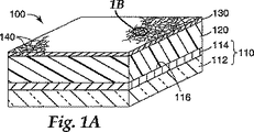
本発明に従って調製される代表的な光化学センサを図1Aに示す。ここで図1Aを参照すると、光化学センサ100は、主反射表面116を有する反射基板110を含む。一部の実施形態では、反射基板110は、表面に任意の反射層114を備えた任意の基材112を含む。検出層120は、表面116の少なくとも一部分上に配置された本質的に微小多孔性のポリマーを含む。パラジウム金属を含む半反射金属層130は、層120の少なくとも一部分上に配置され、また層中に微細なクラックの網目構造140を有する。突出部170(図1Bに示される)は、検出層120から半反射金属層130を貫いて延びる。
A typical photochemical sensor prepared in accordance with the present invention is shown in FIG. 1A. Referring now to FIG. 1A, the
反射基板は、反射表面を有するいずれの基板であってもよい。反射基板は、一体型の物体であってよく、比較的厚くても薄くてもよい。一体型の反射基板の例としては、反射金属箔又はシートが挙げられる。任意に、反射基板は、表面に反射層を備えた基材を含んでもよい。 The reflective substrate may be any substrate having a reflective surface. The reflective substrate may be an integral object and may be relatively thick or thin. Examples of the integrated reflective substrate include a reflective metal foil or sheet. Optionally, the reflective substrate may include a substrate with a reflective layer on the surface.
存在する場合、基材は、任意の反射層に支持をもたらすことのできるいずれか好適な材料を含んでよい。それは、可撓性であっても非可撓性であってもよい。基材材料は、用途に適応させることができる。典型的に、真空蒸着プロセスにおいて使用するのに好適である。代表的な基材としては、高分子フィルム、ガラス、セラミックス、及び金属が挙げられる。基材材料は、検体がそれを通り抜けることのできる穴の配列を含むように設計されることによって、検体透過性にすることができ得る。さらに、基材材料は、検体がそれを通り抜けることのできる織布又は不織布材料、メッシュ、若しくはフィルタ膜であってよい。 When present, the substrate may comprise any suitable material that can provide support to any reflective layer. It can be flexible or inflexible. The substrate material can be adapted to the application. It is typically suitable for use in a vacuum deposition process. Typical base materials include polymer films, glass, ceramics, and metals. The substrate material can be made analyte permeable by being designed to include an array of holes through which the analyte can pass. Further, the substrate material may be a woven or non-woven material, mesh, or filter membrane through which the specimen can pass.
反射基板(例えば、任意の反射層を含む)は、反射層を形成できるいずれの材料を含んでよい。典型的に、材料は、厚さ20nm〜200nmで完全反射性であるが、また、他の厚さも使用されてよい。例えば、材料のより薄い層は、典型的に、反射層を半反射性にするために使用することができる。代表的な好適な材料としては、アルミニウム、クロム、金、ニッケル、チタン、パラジウム、白金、ケイ素、及び銀など、金属及び半金属が挙げられる。金属及び/又は半金属の組合せ(例えば、金−パラジウム又はニッケル−クロムなど)も使用されてよい。反射基板に含めてよい他の好適な材料としては、例えば、酸化クロム及び酸化チタンなどの反射性金属酸化物が挙げられる。反射基板は、典型的に、半反射層よりも反射性にされるが、時には、例えば検体の存在に対する応答をセンサフィルムのどちらの側からも見られるように、反射層及び半反射層の反射率を同一にすることが望ましい。一部の実施形態では、反射基板は、また、それを通って検体が検出層に侵入できる穴又は他の開いた領域を作り出すようにエッチング又は穿孔されてもよいが、これは、必要条件ではない。 The reflective substrate (eg, including any reflective layer) may include any material that can form a reflective layer. Typically, the material is fully reflective at a thickness of 20 nm to 200 nm, but other thicknesses may also be used. For example, thinner layers of material can typically be used to make the reflective layer semi-reflective. Exemplary suitable materials include metals and metalloids such as aluminum, chromium, gold, nickel, titanium, palladium, platinum, silicon, and silver. Combinations of metals and / or metalloids (eg, gold-palladium or nickel-chromium, etc.) may also be used. Other suitable materials that may be included in the reflective substrate include, for example, reflective metal oxides such as chromium oxide and titanium oxide. The reflective substrate is typically made more reflective than the semi-reflective layer, but sometimes the reflective layer and the semi-reflective layer reflect so that, for example, a response to the presence of the analyte can be seen from either side of the sensor film. It is desirable to have the same rate. In some embodiments, the reflective substrate may also be etched or perforated to create holes or other open areas through which analytes can enter the detection layer, although this may be necessary. Absent.
本発明の一部の代表的な実施形態では、任意の反射層は、少なくとも90パーセント反射性(すなわち、少なくとも10パーセント透過性)であり、一部の実施形態では、99パーセント反射性(すなわち、1パーセント透過性)である。本発明の他の代表的な実施形態では、任意の反射層は、半反射層であり、反射層は、20パーセント〜90パーセント反射性又は30パーセント〜70パーセント反射性など、少なくとも20パーセント反射性である。 In some exemplary embodiments of the invention, any reflective layer is at least 90 percent reflective (ie, at least 10 percent transmissive), and in some embodiments, 99 percent reflective (ie, 1 percent permeability). In other exemplary embodiments of the invention, the optional reflective layer is a semi-reflective layer, and the reflective layer is at least 20 percent reflective, such as 20 percent to 90 percent reflective or 30 percent to 70 percent reflective. It is.
検出層は、検体が存在しない状態でセンサによって反射される光と比べてセンサによって反射される光の観察される色の変化をもたらす、検体を取り込んだときに光学的厚さ(検出層の物理的厚さ(d)及び屈折率(n)によって決まる、光学的厚さ=n・d)の変化を起こす1つ又はそれより多くの本質的に微小多孔性のポリマーを含む。 The detection layer has an optical thickness (physical of the detection layer) when the analyte is captured, resulting in a change in the observed color of the light reflected by the sensor compared to the light reflected by the sensor in the absence of the analyte. One or more intrinsically microporous polymers that cause a change in optical thickness = n · d), depending on the thickness (d) and refractive index (n).
検出層は、任意に、2つ又はそれ以上の副層を含んでもよい。任意の副層の1つ若しくはそれより多くは、不連続又はパターン状であってよい。任意の副層は、様々な高分子材料を含んでよく、また、様々な検体を吸着してよく、及び/又は1つ若しくはそれより多くの検体に対して様々な感度を有してよい。任意の副層は、様々な構成を有してよく、例えば、積み重ねられても、横に並べられてもよい。 The detection layer may optionally include two or more sublayers. One or more of the optional sublayers may be discontinuous or patterned. An optional sublayer may comprise various polymeric materials, may adsorb various analytes, and / or have various sensitivities to one or more analytes. The optional sublayers can have a variety of configurations, for example, stacked or arranged side by side.
一部の実施形態では、少なくとも1つの任意の副層は、例えば、光学干渉によって色を生み出す適切な厚さの透明な金属酸化物、金属窒化物、及び金属酸窒化物などの無機材料を含んでよい。好適な無機材料の具体例としては、酸化ケイ素、窒化ケイ素、酸窒化ケイ素、酸化アルミニウム、酸化チタン、窒化チタン、酸窒化チタン、酸化スズ、酸化ジルコニウム、及びそれらの組合せが挙げられる。また、ゼオライトなどの他の無機材料も、(1つ又は複数の)副層で使用するのに好適である。任意の(1つ又は複数の)副層は、微小多孔性、多孔性、又は非多孔性であってよい。 In some embodiments, the at least one optional sublayer comprises an inorganic material such as a transparent metal oxide, metal nitride, and metal oxynitride of an appropriate thickness that produces color by optical interference, for example. It's okay. Specific examples of suitable inorganic materials include silicon oxide, silicon nitride, silicon oxynitride, aluminum oxide, titanium oxide, titanium nitride, titanium oxynitride, tin oxide, zirconium oxide, and combinations thereof. Other inorganic materials such as zeolite are also suitable for use in the sublayer (s). The optional sublayer (s) may be microporous, porous, or non-porous.
少なくとも1つの任意の副層に含めてよい他の材料としては、米国特許出願第11/275,277号(代理人番号61197US002号)、名称「プラズマ蒸着された微小多孔性の検体検出層(PLASMA DEPOSITED MICROPOROUS ANALYTE DETECTION LAYER)」(2005年12月21日出願)に開示されているような、非晶質のランダム共有結合網目薄フィルム(amorphous random covalent network thin films)が挙げられる。 Other materials that may be included in at least one optional sublayer include U.S. Patent Application No. 11 / 275,277 (Attorney No. 61197 US002), entitled "Plasma Deposition Microporous Detecting Layer (PLASMA). DEPOSITED MICROPOROUS ANALYTE DETECTION LAYER ”(filed on Dec. 21, 2005), and amorphous random covalent network thin films.
典型的に、検出層の物理的厚さは、150ナノメートル〜1200ナノメートルの範囲、例えば、500ナノメートル〜900ナノメートルの範囲であるが、また、より薄い及びより厚い検出層も使用されてよい。 Typically, the physical thickness of the detection layer is in the range of 150 nanometers to 1200 nanometers, for example, in the range of 500 nanometers to 900 nanometers, although thinner and thicker detection layers are also used. It's okay.
検出層の厚さは、パターン状であってよい。このことは、検体の存在が検出層の屈折率変化を引き起こし、それによってパターンを消失させる(例えば、一部分が光学的厚さを隣接部分と同じ光学的厚さに変化させるとき)、又はパターンを出現させる(例えば、一部分が、隣接部分とは異なる光学的厚さをもつような光学的厚さ変化を起こすとき)ようにセンサが設計されるときに、望ましい可能性がある。 The thickness of the detection layer may be a pattern. This means that the presence of the analyte causes a change in the refractive index of the detection layer, thereby causing the pattern to disappear (eg, when one part changes the optical thickness to the same optical thickness as an adjacent part), or It may be desirable when the sensor is designed to appear (eg, when an optical thickness change occurs such that a portion has a different optical thickness than an adjacent portion).
検出層は、追加のポリマー構成成分、例えば、本質的に微小多孔性のポリマーである構成成分の少なくとも1つとの均質又は不均質ブレンドをさらに含んでよい。 The detection layer may further comprise a homogeneous or heterogeneous blend with at least one additional polymer component, for example a component that is essentially a microporous polymer.
本明細書で使用するとき、用語「本質的に微小多孔性のポリマー」とは、処理又はテンプレート調製によるのではなくその分子構造に起因した微小多孔性を有する有機ポリマーを意味する。さらに、本質的に微小多孔性のポリマーは、少なくとも10パーセント、例えば、少なくとも15パーセント、又はさらに少なくとも30パーセントの自由体積を有する。 As used herein, the term “essentially microporous polymer” means an organic polymer that has microporosity due to its molecular structure rather than by processing or template preparation. Furthermore, the inherently microporous polymer has a free volume of at least 10 percent, such as at least 15 percent, or even at least 30 percent.
ポリマーに適用されるとき、用語「自由体積」とは、ポリマーの分子によって実際に占有されていないポリマーの体積を指す。ガス種で接近可能な自由体積は、例えば、ブルナウアー・エメット・テラー(Brunauer-Emmett-Teller)(BET)、バレット・ジョイナー・ハレンダ(Barrett-Joyner-Halenda)(BJH)、又はホルバート・カワゾエ(Horvath-Kawazoe)分析と結び付けられた気体吸着技術を含め、様々な既知の方法によって容易に決定する可能性がある。例えば、気体吸着技術に関する詳細は、S.J.グレッグ(S.J.Gregg)及びK.S.W.シン(K.S.W.Sing)によって「吸着、表面積、及び多孔性(Adsorption,Surface Area,and Porosity)」、第2版、アカデミックプレス(Academic Press)、ロンドン(1982年)で報告されている。 When applied to a polymer, the term “free volume” refers to the volume of the polymer that is not actually occupied by the molecules of the polymer. The free volume accessible by the gas species is, for example, Brunauer-Emmett-Teller (BET), Barrett-Joyner-Halenda (BJH), or Holbert Kawazoe (Horvath). -Kawazoe) may be readily determined by various known methods, including gas adsorption techniques coupled with analysis. For example, details on gas adsorption technology can be found in S.A. J. et al. Greg (S.J.Gregg) and K.M. S. W. Reported by K.S.W.Sing in “Adsorption, Surface Area, and Porosity”, 2nd edition, Academic Press, London (1982).
典型的に、有用な本質的に微小多孔性のポリマーは、単独と見なされるかそれらの組合せと見なされるかにかかわらず、気体吸着によって測定したときに1グラム当たり少なくとも0.1ミリリットル(0.1cc/g)、例えば、1グラム当たり少なくとも0.2ミリリットル(0.2cc/g)、又はさらに1グラム当たり少なくとも0.5ミリリットル(0.5cc/g)の接近可能な総細孔容積を有するが、また、その範囲外の値も使用されてよい。さらに、平均直径が0.3ナノメートル〜20ナノメートルの範囲の細孔由来の気体吸着によって測定したときに、少なくとも25パーセントの総細孔容積を有する本質的に微小多孔性のポリマーから、有用な結果が得られることが判明しているが、また、外側の孔径分布も使用されてよい。 Typically, useful essentially microporous polymers, whether considered alone or a combination thereof, are at least 0.1 milliliters per gram (.0.1) as measured by gas adsorption. 1 cc / g), for example having an accessible total pore volume of at least 0.2 milliliters per gram (0.2 cc / g), or even at least 0.5 milliliters per gram (0.5 cc / g) However, values outside that range may also be used. Furthermore, useful from essentially microporous polymers having a total pore volume of at least 25 percent as measured by gas adsorption from pores with average diameters ranging from 0.3 nanometers to 20 nanometers. Although it has been found that good results are obtained, an outer pore size distribution may also be used.
多くの本質的に微小多孔性のポリマーが知られている。例えば、化学コミュニケーション(Chemical Communications)、2004年、(2)、230〜231頁、バッド(Budd)らが、剛性(rigid)及び/又はねじ曲がった(contorted)モノマービルディングブロック間のジベンゾジオキサン結合を含む、一連の本質的に微小多孔性の材料を報告している。ポリマーのこのファミリーの代表的なメンバーとしては、スキーム1に従って表1に示される構成成分A(例えば、A1、A2、又はA3)と構成成分B(例えば、B1、B2、又はB3)との縮合によって生成されるものが挙げられる。 Many inherently microporous polymers are known. For example, Chemical Communications, 2004, (2), 230-231, Budd et al. Described dibenzodioxane bonds between rigid and / or contorted monomer building blocks. A series of essentially microporous materials are reported, including. Representative members of this family of polymers include condensation of component A (eg, A1, A2, or A3) shown in Table 1 according to Scheme 1 with component B (eg, B1, B2, or B3). Can be generated.

さらに好適な構成成分A及びB、並びに得られる本質的に微小多孔性のポリマーは、当該技術分野において既知であり、例えば、バッド(Budd)ら、材料化学雑誌(Journal of Materials Chemistry)、2005年、第15巻、1977〜1986頁、及びマッコーウン(McKeown)ら、化学、ヨーロッパ雑誌(Chemistry, A European Journal)、2005年、第11巻、2610〜2620頁、及びPCT国際公開出願WO2005/012397A2(マッコーウン(McKeown)ら)に報告されている。 Further suitable components A and B and the resulting essentially microporous polymers are known in the art, for example, Budd et al., Journal of Materials Chemistry, 2005. 15, 1977-1986, and McKeown et al., Chemistry, A European Journal, 2005, 11, 261-2620, and PCT International Publication Application WO2005 / 012397A2. (McKeown et al.).
そのようなポリマーは、例えば、A1(5,5’,6,6’−テトラヒドロキシ−3,3,3’,3’−テトラメチル−1,1’−スピロビスインダン)などのビス−カテコールが、塩基性条件下で、例えば、B1(テトラフルオロテレフタロニトリル)などのフッ素化アレーンと反応させられる逐次重合によって、合成することができる。得られるポリマーの主鎖の剛性(rigidity)及びねじ曲がった(contorted)性質ゆえに、これらのポリマーは、固体状態で密に充填することができず、したがって、少なくとも10パーセントの自由体積を有し、本質的に微小多孔性である。 Such polymers are, for example, bis-catechols such as A1 (5,5 ′, 6,6′-tetrahydroxy-3,3,3 ′, 3′-tetramethyl-1,1′-spirobisindane). Can be synthesized by sequential polymerization, for example, by reacting with a fluorinated arene such as B1 (tetrafluoroterephthalonitrile) under basic conditions. Due to the rigidity and contorted nature of the resulting polymer backbone, these polymers cannot be tightly packed in the solid state and thus have a free volume of at least 10 percent, It is inherently microporous.
本質的に微小多孔性のポリマーは、典型的に、例えばテトラヒドロフランなどの有機溶媒に可溶性であり、ゆえに、溶液から(例えば、スピンコーティング、ディップコーティング、又はバーコーティングによって)フィルムとしてキャスティングすることができる。しかし、これらのポリマーの溶液から作製されるフィルムの特徴(接近可能な厚さ、光学的透明度、及び/又は外観)が、フィルムをキャスティングするために使用される溶媒又は溶媒系に応じて著しく異なる場合があることが見出されている。例えば、分子量のより高い本質的に微小多孔性のポリマーは、本明細書に記載の光化学センサで使用するのに望ましい特性を備えたフィルムを作り出すためには、比較的独特な溶媒(例えば、シクロヘキセンオキシド又はテトラヒドロピラン)からキャスティングされる必要がある場合がある。溶液コーティング方法に加えて、検出層は、他のいずれか好適な方法によって反射基板に適用されてよい。 Intrinsically microporous polymers are typically soluble in organic solvents such as tetrahydrofuran, and can therefore be cast as a film from solution (eg, by spin coating, dip coating, or bar coating). . However, the characteristics (accessible thickness, optical clarity, and / or appearance) of films made from solutions of these polymers vary significantly depending on the solvent or solvent system used to cast the film. It has been found that there are cases. For example, higher molecular weight inherently microporous polymers may be used to produce relatively unique solvents (eg, cyclohexene) to produce films with desirable properties for use in the photochemical sensors described herein. Oxide or tetrahydropyran) may need to be cast. In addition to the solution coating method, the detection layer may be applied to the reflective substrate by any other suitable method.
検出層及び/又は本質的に微小多孔性のポリマーは、望むなら、例えば高エネルギー放射線法によって、架橋されてよい。 The detection layer and / or the essentially microporous polymer may be crosslinked if desired, for example by high energy radiation methods.
反射層及び半反射層は、半反射層を作製するために選択される技術が微細なクラックの網目構造を有するほぼ連続的な半反射層をもたらす、蒸発、スパッタリング、化学蒸着(CVD)、プラズマ蒸着、火炎堆積(flame deposition)、又は他のいずれかの技術などの標準的な蒸気コーティング技術によって検出層上に形成されてよい。反射層及び半反射層は、同一又は異なる技術を使用して作製されてよい。 Reflective layer and semi-reflective layer are evaporation, sputtering, chemical vapor deposition (CVD), plasma, where the technique selected to make the semi-reflective layer results in a nearly continuous semi-reflective layer with a fine crack network It may be formed on the detection layer by standard vapor coating techniques such as vapor deposition, flame deposition, or any other technique. The reflective layer and semi-reflective layer may be made using the same or different techniques.
本発明によれば、本質的に微小多孔性のポリマーの熱処理が、例えば本明細書に記載の光化学センサにおけるそれらポリマーの性能を劇的に改善できることが見出されている。 In accordance with the present invention, it has been found that heat treatment of inherently microporous polymers can dramatically improve the performance of those polymers in, for example, the photochemical sensors described herein.
半反射金属層は、パラジウムを、純粋な金属としてか、又は、例えば、銅、水銀、ケイ素、アルミニウム、ロジウム、イリジウム、ニッケル、クロム、オスミウム、金、又は銀など、1つ又はそれより多くの追加の金属又は半金属との組合せとして含む。 The semi-reflective metal layer can be palladium as pure metal or one or more such as, for example, copper, mercury, silicon, aluminum, rhodium, iridium, nickel, chromium, osmium, gold, or silver. In combination with additional metals or metalloids.
半反射金属層は、検出層とは異なる屈折率を有する透過性のほぼ連続的な層を形成する。広くは、半反射金属層は、それが半反射性のままで、微細なクラックの網目構造を有する限り、いずれの厚さを有してもよい。典型的に、これらの特性は、3ナノメートル〜10ナノメートルの厚さで達成されるが、また、他の厚さも使用されてもよい。所望の厚さは、典型的に、層を形成するために使用される材料、層がその上に堆積される材料、検出される検体、及び検体を運ぶ媒体によって決まる。 The semi-reflective metal layer forms a transmissive substantially continuous layer having a different refractive index than the detection layer. In general, the semi-reflective metal layer may have any thickness as long as it remains semi-reflective and has a fine crack network. Typically, these properties are achieved with a thickness of 3 nanometers to 10 nanometers, although other thicknesses may also be used. The desired thickness typically depends on the material used to form the layer, the material on which the layer is deposited, the analyte to be detected, and the medium carrying the analyte.
光化学センサは、追加のいずれかの層がセンサの光学系に著しい及び悪い影響を与えない限り、前述の要素のいずれかの間に追加の層を含んでよい。代表的な追加の層は、結合層(tie layers)及び構造層(structural layers)を含む。 Photochemical sensors may include additional layers between any of the aforementioned elements, as long as any additional layers do not significantly and adversely affect the sensor optics. Typical additional layers include tie layers and structural layers.
本発明による光化学センサは、クラックを広がらせるのに十分な温度で検出層及び半反射金属層を分子酸素の存在下で加熱する追加工程によって、米国特許出願公開第2004/0184948A1(ラコウ(Rakow)ら)に記載の手順に概ね従い製作されてよい。典型的に、200℃〜225℃の範囲の温度のオーブン内で少なくとも30分間加熱することが効果的であるが、他の温度及び持続時間も使用されてよい。250℃以上の温度では、ポリマーの分解が大規模に起こって問題となることがある。 The photochemical sensor according to the present invention is disclosed in US Patent Application Publication No. 2004 / 0184948A1 (Rakow) by an additional step of heating the detection layer and semi-reflective metal layer in the presence of molecular oxygen at a temperature sufficient to spread cracks. Etc.) and may be manufactured according to the procedure described in FIG. Typically, it is effective to heat in an oven at a temperature in the range of 200 ° C. to 225 ° C. for at least 30 minutes, although other temperatures and durations may be used. At temperatures above 250 ° C., polymer degradation can occur on a large scale and become a problem.
本発明による光化学センサは、例えば、センサが検体に曝露されたときに、そのセンサから得られる応答から、検体の濃度を計算又は推定するのに有用である。検体は、例えば、気体(例えば、有機蒸気)又は液体であってよい。 The photochemical sensor according to the present invention is useful, for example, for calculating or estimating the concentration of an analyte from a response obtained from the sensor when the sensor is exposed to the analyte. The analyte can be, for example, a gas (eg, organic vapor) or a liquid.
センサ応答は、典型的に、比色分析的な性質(例えば、観察される色の変化として)であるが、他の応答も有用な場合がある。例えば、光化学センサは、センサと、光源と、所望により、色の変化、あるいはスペクトルのピーク位置又は強度の変化についてセンサを監視する手段とを含むシステムにおいて使用されてよい。本発明のセンサは、典型的に、反射分光法によって都合よく監視されてよい。光源は、天然又は人工光源とすることができる。監視は、様々な方法で実施することができる。それは、視覚的に、光検出器を用いて、又は他の好適な手段によって、実施することができる。 The sensor response is typically colorimetric in nature (eg, as an observed color change), but other responses may be useful. For example, a photochemical sensor may be used in a system that includes a sensor, a light source, and means for monitoring the sensor for changes in color, or spectral peak position or intensity, as desired. The sensors of the present invention may typically be conveniently monitored by reflection spectroscopy. The light source can be a natural or artificial light source. Monitoring can be implemented in various ways. It can be done visually, with a photodetector or by other suitable means.
配列を形成するために、2つ又はそれ以上の光化学センサを組み合わせてよい。配列は、いずれか好適な構成であってよい。例えば、配列は、横に並んだ2つ又はそれ以上のセンサを含んでよく、又はセンサは、基板の両側に取り付けられても、あるいは基板の両側に構築されてもよい。センサは、同一の種類のものであっても、異なるものであってもよい。 Two or more photochemical sensors may be combined to form an array. The arrangement may be any suitable configuration. For example, the array may include two or more sensors side by side, or the sensors may be mounted on either side of the substrate or constructed on both sides of the substrate. The sensors may be of the same type or different.
少なくとも1つの実施形態では、検体は、その検体に曝露されたときの検出層の光学的厚さの変化によって検出される。そのような変化は、典型的に、可視光範囲で観察可能であり、しばしば人間の裸眼によって検出することができる。しかし、UV、赤外線、又は近赤外線など、他の光源に曝されたときの光学的厚さの変化を検出できるように、センサを設計することができる。また、様々な検出機構を使用することもできる。好適な検出機構の例としては、分光光度計、光ファイバ分光光度計、及び光検出器、例えば、電荷結合素子(ccd)、デジタルカメラなどが挙げられる。 In at least one embodiment, the analyte is detected by a change in the optical thickness of the detection layer when exposed to the analyte. Such changes are typically observable in the visible light range and can often be detected by the human naked eye. However, the sensor can be designed to detect changes in optical thickness when exposed to other light sources, such as UV, infrared, or near infrared. Various detection mechanisms can also be used. Examples of suitable detection mechanisms include spectrophotometers, fiber optic spectrophotometers, and photodetectors such as charge coupled devices (ccd), digital cameras, and the like.
本発明の目的および利点を以下の非限定的な実施例によってさらに例示するが、これらの実施例の中で挙げる特定の材料および材料の量、並びに他の条件および詳細は、本発明を不当に限定するように解釈されるべきではない。 The objects and advantages of the present invention are further illustrated by the following non-limiting examples, although the specific materials and amounts of materials listed in these examples, as well as other conditions and details, unduly limit the present invention. It should not be construed as limiting.
特に記載のない限り、実施例及び本明細書の残りの部分における全ての部、百分率、比率などは、すべて重量によるものであり、実施例で使用される全ての溶媒及び試薬は、例えばミズーリ州セントルイス(Saint Louis,Missouri)、シグマ・アルドリッチ社(Sigma-Aldrich Company)などの一般的な化学薬品供給元から得られた又は入手可能なものであり、又は従来の方法によって合成し得る可能性がある。 Unless otherwise noted, all parts, percentages, ratios, etc. in the examples and the rest of the specification are by weight, and all solvents and reagents used in the examples are, for example, Obtained or available from common chemical suppliers such as Saint Louis, Missouri, Sigma-Aldrich Company, or could be synthesized by conventional methods is there.
試験方法
表面積及び細孔容積測定
総細孔容積は、75ポイント微小細孔分析を使用して製造業者の指示に従って操作される商品表記「カンタロームオートソーブ1C(QUANTACHROME AUTOSORB 1C)」(カンタクロームインスツルメンツ(Quantachrome Instruments)、フロリダ州ボイントンビーチ(Boynton Beach,Florida))として入手可能な気体吸着分析器を使用する窒素吸着によって測定した。
Test method Surface area and pore volume measurement The total pore volume is manipulated according to the manufacturer's instructions using 75-point micropore analysis "QUANTACHROME AUTOSORB 1C" (Cantachrome Instruments) (Quantachrome Instruments), measured by nitrogen adsorption using a gas adsorption analyzer available as Boynton Beach, Florida.
調製実施例P1〜P5
表2(以下)に示される試薬、条件、及びポリマーの説明を使用し、バッド(Budd)らの先端材料(Advanced Materials)、2004年、第16巻、第5号、456頁〜459頁に報告されている手順に概ね従って、モノマーBC及びモノマーFAからポリマーを調製した。
Preparation Examples P1-P5
Using the reagents, conditions, and polymer descriptions shown in Table 2 (below), see Budd et al. Advanced Materials, 2004, Vol. 16, No. 5, pages 456-459. In general accordance with the reported procedure, a polymer was prepared from monomer BC and monomer FA.
表2において。「NM」は、測定されていないことを意味し、「総細孔容積」は、370ナノメートル未満の平均直径をもつ細孔を指す。 In Table 2. “NM” means not measured and “total pore volume” refers to pores having an average diameter of less than 370 nanometers.
各ポリマーをTHFに溶解させ、メタノールから3回沈殿させ、次いで室温で真空下で乾燥させた。いずれの場合にも、明るい黄色の固体が得られた。 Each polymer was dissolved in THF, precipitated from methanol three times and then dried under vacuum at room temperature. In either case, a bright yellow solid was obtained.
実施例1〜4及び比較実施例C1〜C3。 Examples 1-4 and comparative examples C1-C3.
厚さ100ナノメートルのアルミニウムコーティングを有するガラススライドを、反射基板として使用した。調製実施例P1からのポリマーをTHFに溶解させて、3重量パーセント溶液を得て、それを表3に示される速度でアルミニウム上にスピンコーティングした。スピンコーティング後、厚さ5ナノメートル(nm)のAu/Pd(Au対Pdの重量比60:40)層を、ポリマー上にスパッタコーティングした。こうして調製されたサンプルを、表3(以下)に示される温度にしたがって30分間ベルト炉内で空気中で加熱して、光化学センサを形成し、ポリマー層の色の変化を書き留めた。 A glass slide with a 100 nanometer thick aluminum coating was used as the reflective substrate. The polymer from Preparative Example P1 was dissolved in THF to give a 3 weight percent solution that was spin coated onto aluminum at the rate shown in Table 3. After spin coating, a 5 nanometer (nm) Au / Pd (Au to Pd weight ratio 60:40) layer was sputter coated onto the polymer. The sample thus prepared was heated in air in a belt furnace for 30 minutes according to the temperature shown in Table 3 (below) to form a photochemical sensor and noted the color change of the polymer layer.
加熱されたサンプルのUV/VIS反射分光法で、250℃で加熱されたサンプルはUV/VIS反射スペクトルにおける明確なピークの喪失を示し、さらに200℃で加熱されたサンプルは最大反射率波長の大きなシフトを示したことが示された。 In the UV / VIS reflection spectroscopy of the heated sample, the sample heated at 250 ° C. shows a clear peak loss in the UV / VIS reflection spectrum, and the sample heated at 200 ° C. has a higher maximum reflectance wavelength. It was shown that it showed a shift.
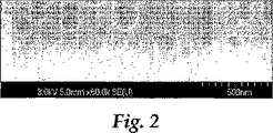
図2は、倍率60,000倍で撮影された、加熱前の実施例1の反復実験の電子顕微鏡写真である。 FIG. 2 is an electron micrograph of an iterative experiment of Example 1 before heating, taken at a magnification of 60,000.
図3は、倍率60,000倍で撮影された、加熱後の実施例1の反復実験の電子顕微鏡写真である。 FIG. 3 is an electron micrograph of the repeated experiment of Example 1 after heating, taken at a magnification of 60,000.
(実施例5)
実施例1の多層フィルムサンプルを、低濃度のトルエン蒸気に対する応答について試験した。最大反射率ピーク波長における5ナノメートルの赤色シフトが、50百万分率(ppm)のトルエン蒸気で観察され、最大反射率ピーク波長における約50ナノメートルの赤色シフトが、2000ppm濃度で観察された。
(Example 5)
The multilayer film sample of Example 1 was tested for response to low concentrations of toluene vapor. A 5 nanometer red shift at the maximum reflectance peak wavelength was observed with 50 parts per million (ppm) toluene vapor and an approximately 50 nanometer red shift at the maximum reflectance peak wavelength was observed at 2000 ppm concentration. .
比較実施例C4
実施例1の多層フィルムの代わりに比較実施例1の多層フィルムを使用したことを除いて、実施例5を繰り返した。このフィルムについて、2000ppm以下のトルエン蒸気濃度では、最大反射率ピーク波長のシフト位置は、観察されなかった。
Comparative Example C4
Example 5 was repeated except that the multilayer film of Comparative Example 1 was used instead of the multilayer film of Example 1. With respect to this film, the shift position of the maximum reflectance peak wavelength was not observed at a toluene vapor concentration of 2000 ppm or less.
比較実施例C5及びC6
2つの多層フィルムアセンブリを調製した。厚さ100ナノメートルのアルミニウム層を含むガラススライドをベース基板として使用した。調製実施例P3からのポリマーをTHFに溶解させて、5重量パーセント溶液を得て、それを1000rpmでアルミニウム上にスピンコーティングした。スピンコーティング後、両方のアセンブリで厚さ5nmのAl層をポリマー上に蒸発によって堆積させた。両方のコーティングされたアセンブリは、金属コーティング後、黄−赤の色相によって特徴付けられた。比較実施例C5を200℃で30分にわたってベルト炉内で加熱したが、黄−赤の色相の変化をもたらさなかった。比較実施例C6は、加熱処理しなかった。比較実施例C5及びC6を、低濃度のトルエン蒸気に対するそれらの応答について試験した。いずれのセンサも、2000ppmのトルエン蒸気ほどの高い濃度に対しては反射率スペクトル応答の変化を示さなかった。
Comparative Examples C5 and C6
Two multilayer film assemblies were prepared. A glass slide containing a 100 nanometer thick aluminum layer was used as the base substrate. The polymer from Preparative Example P3 was dissolved in THF to give a 5 weight percent solution that was spin coated onto aluminum at 1000 rpm. After spin coating, a 5 nm thick Al layer was deposited by evaporation on the polymer in both assemblies. Both coated assemblies were characterized by a yellow-red hue after metal coating. Comparative Example C5 was heated in a belt furnace at 200 ° C. for 30 minutes and did not result in a yellow-red hue change. Comparative Example C6 was not heat treated. Comparative Examples C5 and C6 were tested for their response to low concentrations of toluene vapor. None of the sensors showed a change in reflectance spectral response for concentrations as high as 2000 ppm toluene vapor.
比較実施例C7及びC8
2つの多層フィルムアセンブリを調製した。厚さ100ナノメートルのアルミニウム層を含むガラススライドをベース基板として使用した。調製実施例P3からのポリマーをTHFに溶解させて、5重量パーセント溶液を得て、それを1000rpmでアルミニウム上にスピンコーティングした。スピンコーティング後、両方のアセンブリで厚さ5nmのTi層をポリマー上に蒸発によって堆積させた。両方のコーティングされたアセンブリは、金属コーティング後、黄−赤の色相によって特徴付けられた。比較実施例C7を200℃で30分にわたってベルト炉内で加熱したが、黄−赤の色相の変化をもたらさなかった。比較実施例C8は、加熱処理しなかった。比較実施例C7及びC8を、低濃度のトルエン蒸気に対するそれらの応答について試験した。比較実施例C7及びC8のいずれも、2000ppmのトルエン蒸気ほどの高い濃度に対しては反射率スペクトル応答の変化を示さなかった。
Comparative Examples C7 and C8
Two multilayer film assemblies were prepared. A glass slide containing a 100 nanometer thick aluminum layer was used as the base substrate. The polymer from Preparative Example P3 was dissolved in THF to give a 5 weight percent solution that was spin coated onto aluminum at 1000 rpm. After spin coating, a 5 nm thick Ti layer was deposited on the polymer by evaporation in both assemblies. Both coated assemblies were characterized by a yellow-red hue after metal coating. Comparative Example C7 was heated in a belt furnace at 200 ° C. for 30 minutes and did not result in a yellow-red hue change. Comparative Example C8 was not heat treated. Comparative Examples C7 and C8 were tested for their response to low concentrations of toluene vapor. None of Comparative Examples C7 and C8 showed a change in reflectance spectral response for concentrations as high as 2000 ppm toluene vapor.
比較実施例C9及びC10。 Comparative Examples C9 and C10.
2つの多層フィルムアセンブリを調製した。厚さ100ナノメートルのアルミニウム層を含むガラススライドをベース基板として使用した。調製実施例P4からのポリマーをTHFに溶解させて、5重量パーセント溶液を得て、それを1500rpmでアルミニウム上にスピンコーティングした。スピンコーティング後、厚さ5nmのクロム層を、各アセンブリのポリマー上に蒸発によって堆積させた。両方のコーティングされたアセンブリは、金属コーティング後、黄−緑の色相によって特徴付けられた。比較実施例C9を200℃で30分にわたってベルト炉内で加熱したが、黄−緑の色相の変化をもたらさなかった。比較実施例C10は、加熱処理しなかった。比較実施例C9及びC10を、低濃度のトルエン蒸気に対するそれらの応答について試験した。比較実施例C9及びC10のいずれも、2000ppmのトルエン蒸気ほどの高い濃度に対しては反射率スペクトル応答の変化を示さなかった。 Two multilayer film assemblies were prepared. A glass slide containing a 100 nanometer thick aluminum layer was used as the base substrate. The polymer from Preparative Example P4 was dissolved in THF to give a 5 weight percent solution that was spin coated onto aluminum at 1500 rpm. After spin coating, a 5 nm thick chromium layer was deposited by evaporation on the polymer of each assembly. Both coated assemblies were characterized by a yellow-green hue after metal coating. Comparative Example C9 was heated in a belt furnace at 200 ° C. for 30 minutes and did not result in a yellow-green hue change. Comparative Example C10 was not heat treated. Comparative Examples C9 and C10 were tested for their response to low concentrations of toluene vapor. None of Comparative Examples C9 and C10 showed a change in reflectance spectral response for concentrations as high as 2000 ppm toluene vapor.
実施例6及び比較実施例C11
2つの多層フィルムアセンブリを調製した。厚さ100ナノメートルのアルミニウム層を含むガラススライドをベース基板として使用した。調製実施例P5からのポリマーをクロロベンゼンに溶解させて、4重量パーセント溶液を得て、それを3000rpmで基板上にスピンコーティングした。スピンコーティング後、両方のアセンブリでパラジウム層をポリマー層上にスパッタコーティング(厚さ約5nm)した。コーティングされたアセンブリは、Pd金属被覆後、青−緑の色によって特徴付けられた。実施例6を200℃で30分にわたってベルト炉内で加熱したところ、黄−緑の色相を与える色の変化をもたらした。比較実施例C11は、加熱処理しなかった。実施例6及び比較実施例C11を、トルエン蒸気の濃度に対するそれらの応答について試験した。実施例6は、2000ppmのトルエン蒸気でその可視反射率スペクトルにおける観察可能な応答を示したが、比較実施例C11は、2000ppmのトルエン蒸気まで応答を示さなかった。
Example 6 and Comparative Example C11
Two multilayer film assemblies were prepared. A glass slide containing a 100 nanometer thick aluminum layer was used as the base substrate. The polymer from Preparative Example P5 was dissolved in chlorobenzene to give a 4 weight percent solution, which was spin coated onto the substrate at 3000 rpm. After spin coating, a palladium layer was sputter coated (about 5 nm thick) on the polymer layer in both assemblies. The coated assembly was characterized by a blue-green color after Pd metallization. Example 6 was heated in a belt furnace at 200 ° C. for 30 minutes, resulting in a color change that gave a yellow-green hue. Comparative Example C11 was not heat treated. Example 6 and Comparative Example C11 were tested for their response to toluene vapor concentration. Example 6 showed an observable response in its visible reflectance spectrum with 2000 ppm toluene vapor, while Comparative Example C11 did not show a response until 2000 ppm toluene vapor.
比較実施例C12及びC13。 Comparative Examples C12 and C13.
2つの多層フィルムアセンブリを調製した。厚さ100ナノメートルのアルミニウム層を含むガラススライドをベース基板として使用した。調製実施例P5からのポリマーをクロロベンゼンに溶解させて、4重量パーセント溶液を得て、それを3000rpmでアルミニウム上にスピンコーティングした。スピンコーティング後、両方のアセンブリでニッケル層をポリマー層上にスパッタコーティング(厚さ約5nm)した。両方のコーティングされたアセンブリは、金属コーティング後、黄−緑の色相によって特徴付けられた。比較実施例C12を200℃で30分にわたってベルト炉内で加熱したが、黄−緑の色相の変化はもたらさなかった。比較実施例C13は、加熱処理しなかった。比較実施例C12及びC13を、低濃度のトルエン蒸気に対するそれらの応答について試験した。比較実施例C12及びC13のいずれも、2000ppmのトルエン蒸気ほどの高い濃度に対しては反射率スペクトル応答の変化を示さなかった。 Two multilayer film assemblies were prepared. A glass slide containing a 100 nanometer thick aluminum layer was used as the base substrate. The polymer from Preparative Example P5 was dissolved in chlorobenzene to give a 4 weight percent solution that was spin coated onto aluminum at 3000 rpm. After spin coating, a nickel layer was sputter coated (about 5 nm thick) on the polymer layer in both assemblies. Both coated assemblies were characterized by a yellow-green hue after metal coating. Comparative Example C12 was heated in a belt furnace at 200 ° C. for 30 minutes, but did not produce a yellow-green hue change. Comparative Example C13 was not heat treated. Comparative Examples C12 and C13 were tested for their response to low concentrations of toluene vapor. Neither Comparative Example C12 nor C13 showed a change in reflectance spectral response for concentrations as high as 2000 ppm toluene vapor.
本発明の種々の修正および変更は、本発明の範囲および精神を逸脱しなければ当業者によって行われてよく、また本発明は、本明細書に記載された例示的な実施形態に不当に限定されるべきではないと理解されるべきである。 Various modifications and alterations of this invention may be made by those skilled in the art without departing from the scope and spirit of this invention, and the invention is unduly limited to the exemplary embodiments described herein. It should be understood that it should not be done.
Claims (2)
主表面を有する反射基板を提供する工程と、
少なくとも1つの本質的に微小多孔性のポリマーを含む検出層を前記主表面の少なくとも一部分に添着する工程と、
前記検出層の少なくとも一部分上にほぼ連続的な半反射金属層を堆積させる工程であって、前記半反射金属層は、パラジウムを含みかつ層中に微細な不規則クラックの網目構造を有している、工程と、
前記クラックを広がらせるのに十分な温度で少なくとも前記検出層及び前記半反射金属層を分子酸素の存在下で加熱する工程とを含む、方法。A method for producing a photochemical sensor, comprising:
Providing a reflective substrate having a main surface;
Applying a detection layer comprising at least one essentially microporous polymer to at least a portion of the major surface;
Depositing a substantially continuous semi-reflective metal layer on at least a portion of the detection layer, the semi-reflective metal layer comprising palladium and having a network of fine irregular cracks in the layer; The process,
Heating at least the detection layer and the semi-reflective metal layer in the presence of molecular oxygen at a temperature sufficient to spread the cracks.
前記反射基板の前記主表面の少なくとも一部分上に配置された検出層であって、少なくとも1つの本質的に微小多孔性のポリマーを含む、検出層と、
前記検出層の少なくとも一部分上に配置されたほぼ連続的な半反射金属層と
を含む、光化学センサであって、前記半反射金属層は、パラジウムを含んでおり、前記半反射金属層は、層中に微細な不規則クラックの網目構造を有しており、前記検出層から前記半反射金属層を貫いて延びる複数の突出部が存在する、センサ。A reflective substrate having a main surface;
A detection layer disposed on at least a portion of the major surface of the reflective substrate, the detection layer comprising at least one essentially microporous polymer;
A substantially continuous semi-reflective metal layer disposed on at least a portion of the detection layer, wherein the semi-reflective metal layer comprises palladium, and the semi-reflective metal layer comprises a layer A sensor having a mesh structure of fine irregular cracks therein and having a plurality of protrusions extending from the detection layer through the semi-reflective metal layer.
Applications Claiming Priority (3)
| Application Number | Priority Date | Filing Date | Title |
|---|---|---|---|
| US11/275,268 US7556774B2 (en) | 2005-12-21 | 2005-12-21 | Optochemical sensor and method of making the same |
| US11/275,268 | 2005-12-21 | ||
| PCT/US2006/046386 WO2007075273A1 (en) | 2005-12-21 | 2006-12-05 | Optochemical sensor and method of making the same |
Publications (3)
| Publication Number | Publication Date |
|---|---|
| JP2009521675A JP2009521675A (en) | 2009-06-04 |
| JP2009521675A5 JP2009521675A5 (en) | 2010-01-14 |
| JP4861431B2 true JP4861431B2 (en) | 2012-01-25 |
Family
ID=38173726
Family Applications (1)
| Application Number | Title | Priority Date | Filing Date |
|---|---|---|---|
| JP2008547266A Expired - Fee Related JP4861431B2 (en) | 2005-12-21 | 2006-12-05 | Photochemical sensor and manufacturing method thereof |
Country Status (5)
| Country | Link |
|---|---|
| US (1) | US7556774B2 (en) |
| EP (1) | EP1963852B1 (en) |
| JP (1) | JP4861431B2 (en) |
| CN (1) | CN101331399B (en) |
| WO (1) | WO2007075273A1 (en) |
Families Citing this family (44)
| Publication number | Priority date | Publication date | Assignee | Title |
|---|---|---|---|---|
| US7704751B2 (en) | 2006-09-18 | 2010-04-27 | 3M Innovative Properties Company | Polymeric fluorescent chemical sensor |
| CA2690368A1 (en) * | 2007-06-25 | 2008-12-31 | Qinetiq Limited | Heater suitable for use in a preconcentrator device |
| US8137979B2 (en) * | 2007-06-25 | 2012-03-20 | Qinetiq Limited | Preconcentrator device |
| BRPI0816493A2 (en) * | 2007-10-05 | 2019-02-26 | 3M Innovatie Properties Company | sensor and method for detecting an organic chemical analyte and methods of manufacturing an element of organic chemical analyte detection |
| WO2009045733A2 (en) * | 2007-10-05 | 2009-04-09 | 3M Innovative Properties Company | Organic chemical sensor comprising microporous polymer, and method of use |
| US8647884B2 (en) * | 2008-12-23 | 2014-02-11 | 3M Innovative Properties Company | Organic chemical sensor with microporous organosilicate material |
| KR200474377Y1 (en) * | 2009-01-29 | 2014-09-12 | 쓰리엠 이노베이티브 프로퍼티즈 컴파니 | Monitor for Optical Detection of Organic Analytes |
| AU2010235022B2 (en) | 2009-03-30 | 2013-08-22 | 3M Innovative Properties Company | Optoelectronic methods and devices for detection of analytes |
| BRPI1009623A2 (en) * | 2009-05-22 | 2016-06-28 | 3M Innovative Properties Co | optically questionable sensing element and method for sensing element manufacturing |
| US8336543B2 (en) * | 2009-05-22 | 2012-12-25 | 3M Innovative Properties Company | Filter cartridge having cover for masking service life indicator |
| US8365723B2 (en) * | 2009-05-22 | 2013-02-05 | 3M Innovative Properties Company | Filter cartridge having cone of visibility for end-of-service-life-indicator (ESLI) |
| KR101777078B1 (en) | 2009-05-22 | 2017-09-08 | 쓰리엠 이노베이티브 프로퍼티즈 컴파니 | Multilayer colorimetric sensor arrays |
| US8225782B2 (en) * | 2009-05-22 | 2012-07-24 | 3M Innovative Properties Company | Filter cartridge having location-registered view window for end-of-service-life-indicator (ESLI) |
| US8955515B2 (en) * | 2009-10-23 | 2015-02-17 | 3M Innovative Properties Company | Patterned chemical sensor having inert occluding layer |
| JP6071873B2 (en) | 2010-04-02 | 2017-02-01 | スリーエム イノベイティブ プロパティズ カンパニー | Alignment alignment mechanism for specimen sensor optical reader |
| WO2011123403A1 (en) | 2010-04-02 | 2011-10-06 | 3M Innovative Properties Company | Filter systems including optical analyte sensors and optical readers |
| KR20130014564A (en) | 2010-04-02 | 2013-02-07 | 쓰리엠 이노베이티브 프로퍼티즈 컴파니 | Filter systems including patterned optical analyte sensors and optical readers |
| EP2583090B1 (en) | 2010-06-15 | 2016-04-06 | 3M Innovative Properties Company | Variable capacitance sensors and methods of making the same |
| GB201015397D0 (en) | 2010-09-15 | 2010-10-27 | Univ Cardiff | Polymerisation method |
| GB201015401D0 (en) | 2010-09-15 | 2010-10-27 | Univ Cardiff | Polymers, their method of manufacture and use thereof |
| CN103154714A (en) | 2010-09-30 | 2013-06-12 | 3M创新有限公司 | Sensor element, method of making the same, and sensor device including the same |
| WO2012050686A1 (en) | 2010-09-30 | 2012-04-19 | 3M Innovative Properties Company | Sensor element, method of making the same, and sensor device including the same |
| CN103140749B (en) | 2010-10-01 | 2016-03-30 | 3M创新有限公司 | For making the method that serviceable life, terminal was associated of monitoring device and filter cylinder |
| EP2622321A4 (en) | 2010-10-01 | 2014-03-19 | 3M Innovative Properties Co | Portable monitor for end of service life indication |
| JP6049686B2 (en) * | 2011-03-28 | 2016-12-21 | スリーエム イノベイティブ プロパティズ カンパニー | Sensor with masking layer adhesive |
| WO2012141925A1 (en) * | 2011-04-13 | 2012-10-18 | 3M Innovative Properties Company | Method of detecting volatile organic compounds |
| US9279792B2 (en) | 2011-04-13 | 2016-03-08 | 3M Innovative Properties Company | Method of using an absorptive sensor element |
| US9506888B2 (en) | 2011-04-13 | 2016-11-29 | 3M Innovative Properties Company | Vapor sensor including sensor element with integral heating |
| WO2012174099A1 (en) * | 2011-06-16 | 2012-12-20 | 3M Innovative Properties Company | Surface plasmon resonance sensor element and sensor including the same |
| LU91841B1 (en) * | 2011-07-15 | 2013-01-16 | Ct De Rech Public Gabriel Lippmann | Method for forming gas sensing layers |
| EP2776498B1 (en) * | 2011-11-09 | 2018-12-26 | 3M Innovative Properties Company | Curing compositions for fluoropolymers |
| RU2595665C2 (en) | 2011-12-12 | 2016-08-27 | 3М Инновейтив Пропертиз Компани | System, indicating end of service life, for multi-layer filtering cartridges |
| CN104024848B (en) | 2011-12-13 | 2016-01-20 | 3M创新有限公司 | For identifying the method with the unknown organic compound in quantitative measurement gas medium |
| EP2864770B1 (en) | 2012-06-25 | 2017-09-27 | 3M Innovative Properties Company | Sensor element, method of making, and method of using the same |
| KR20150060819A (en) * | 2012-09-25 | 2015-06-03 | 쓰리엠 이노베이티브 프로퍼티즈 컴파니 | Polymerizable spirobisindane monomers and polymers prepared therefrom |
| WO2014149917A1 (en) | 2013-03-15 | 2014-09-25 | 3M Innovative Properties Company | End of service life indicating systems for layered filter cartridges |
| KR102215926B1 (en) * | 2019-06-28 | 2021-02-17 | 한국생산기술연구원 | Method for manufacturing strain gauge with micro crack |
| US11813926B2 (en) | 2020-08-20 | 2023-11-14 | Denso International America, Inc. | Binding agent and olfaction sensor |
| US11760169B2 (en) | 2020-08-20 | 2023-09-19 | Denso International America, Inc. | Particulate control systems and methods for olfaction sensors |
| US11932080B2 (en) | 2020-08-20 | 2024-03-19 | Denso International America, Inc. | Diagnostic and recirculation control systems and methods |
| US11828210B2 (en) | 2020-08-20 | 2023-11-28 | Denso International America, Inc. | Diagnostic systems and methods of vehicles using olfaction |
| US11636870B2 (en) | 2020-08-20 | 2023-04-25 | Denso International America, Inc. | Smoking cessation systems and methods |
| US11760170B2 (en) | 2020-08-20 | 2023-09-19 | Denso International America, Inc. | Olfaction sensor preservation systems and methods |
| US11881093B2 (en) | 2020-08-20 | 2024-01-23 | Denso International America, Inc. | Systems and methods for identifying smoking in vehicles |
Citations (8)
| Publication number | Priority date | Publication date | Assignee | Title |
|---|---|---|---|---|
| JPS62297223A (en) * | 1986-05-28 | 1987-12-24 | ア−・ファウ・エル ア−・ゲ− | Manufacture of carrier material for optical sensor |
| JPH0580049A (en) * | 1991-07-22 | 1993-03-30 | Fuji Photo Film Co Ltd | Measuring method using dry type analysis element and dry type analysis element |
| JPH0727696A (en) * | 1984-07-06 | 1995-01-31 | Metricor Inc | Optical measuring device using spectral modulation type sensor with optical resonator |
| JP2002054990A (en) * | 2000-08-09 | 2002-02-20 | Sunx Ltd | Optical sensor |
| JP2002168790A (en) * | 2000-11-29 | 2002-06-14 | Sony Corp | Detector of reductive air pollutant, its concentration measure, its detection method and its concentration measuring method |
| US20040062682A1 (en) * | 2002-09-30 | 2004-04-01 | Rakow Neal Anthony | Colorimetric sensor |
| JP2005138434A (en) * | 2003-11-06 | 2005-06-02 | National Institute Of Advanced Industrial & Technology | Structural discoloring material discolored by sorption of substance |
| JP2007530940A (en) * | 2004-03-24 | 2007-11-01 | スリーエム イノベイティブ プロパティズ カンパニー | Colorimetric sensor |
Family Cites Families (10)
| Publication number | Priority date | Publication date | Assignee | Title |
|---|---|---|---|---|
| US5015843A (en) * | 1990-02-15 | 1991-05-14 | Polysense, Inc. | Fiber optic chemical sensors based on polymer swelling |
| AT403746B (en) * | 1994-04-12 | 1998-05-25 | Avl Verbrennungskraft Messtech | OPTOCHEMICAL SENSOR AND METHOD FOR THE PRODUCTION THEREOF |
| JPH08184560A (en) * | 1994-12-28 | 1996-07-16 | Hoechst Japan Ltd | Optical sensor for detecting vapor of organic solvent |
| DE19545414C2 (en) * | 1995-12-06 | 2002-11-14 | Inst Physikalische Hochtech Ev | Optical sensor element |
| US6180318B1 (en) * | 1999-05-19 | 2001-01-30 | 3M Innovative Properties Company | Method of imaging an article |
| US6396616B1 (en) * | 2000-10-10 | 2002-05-28 | 3M Innovative Properties Company | Direct laser imaging system |
| US6878419B2 (en) * | 2001-12-14 | 2005-04-12 | 3M Innovative Properties Co. | Plasma treatment of porous materials |
| JP2004026547A (en) | 2002-06-24 | 2004-01-29 | Nippon Sheet Glass Co Ltd | Heat-insulating laminated glass |
| GB0317557D0 (en) | 2003-07-26 | 2003-08-27 | Univ Manchester | Microporous polymer material |
| US7033667B2 (en) * | 2003-12-18 | 2006-04-25 | 3M Innovative Properties Company | Printed circuits on shrink film |
-
2005
- 2005-12-21 US US11/275,268 patent/US7556774B2/en not_active Expired - Fee Related
-
2006
- 2006-12-05 JP JP2008547266A patent/JP4861431B2/en not_active Expired - Fee Related
- 2006-12-05 CN CN2006800476897A patent/CN101331399B/en not_active Expired - Fee Related
- 2006-12-05 WO PCT/US2006/046386 patent/WO2007075273A1/en active Application Filing
- 2006-12-05 EP EP06838998.0A patent/EP1963852B1/en not_active Not-in-force
Patent Citations (9)
| Publication number | Priority date | Publication date | Assignee | Title |
|---|---|---|---|---|
| JPH0727696A (en) * | 1984-07-06 | 1995-01-31 | Metricor Inc | Optical measuring device using spectral modulation type sensor with optical resonator |
| JPS62297223A (en) * | 1986-05-28 | 1987-12-24 | ア−・ファウ・エル ア−・ゲ− | Manufacture of carrier material for optical sensor |
| JPH0580049A (en) * | 1991-07-22 | 1993-03-30 | Fuji Photo Film Co Ltd | Measuring method using dry type analysis element and dry type analysis element |
| JP2002054990A (en) * | 2000-08-09 | 2002-02-20 | Sunx Ltd | Optical sensor |
| JP2002168790A (en) * | 2000-11-29 | 2002-06-14 | Sony Corp | Detector of reductive air pollutant, its concentration measure, its detection method and its concentration measuring method |
| US20040062682A1 (en) * | 2002-09-30 | 2004-04-01 | Rakow Neal Anthony | Colorimetric sensor |
| JP2006501467A (en) * | 2002-09-30 | 2006-01-12 | スリーエム イノベイティブ プロパティズ カンパニー | Reflective colorimetric sensing element |
| JP2005138434A (en) * | 2003-11-06 | 2005-06-02 | National Institute Of Advanced Industrial & Technology | Structural discoloring material discolored by sorption of substance |
| JP2007530940A (en) * | 2004-03-24 | 2007-11-01 | スリーエム イノベイティブ プロパティズ カンパニー | Colorimetric sensor |
Also Published As
| Publication number | Publication date |
|---|---|
| CN101331399A (en) | 2008-12-24 |
| US20070140907A1 (en) | 2007-06-21 |
| CN101331399B (en) | 2012-09-05 |
| JP2009521675A (en) | 2009-06-04 |
| EP1963852A4 (en) | 2017-09-06 |
| EP1963852B1 (en) | 2018-09-19 |
| US7556774B2 (en) | 2009-07-07 |
| WO2007075273A1 (en) | 2007-07-05 |
| EP1963852A1 (en) | 2008-09-03 |
Similar Documents
| Publication | Publication Date | Title |
|---|---|---|
| JP4861431B2 (en) | Photochemical sensor and manufacturing method thereof | |
| JP5955379B2 (en) | Method for detecting volatile organic compounds | |
| JP5319300B2 (en) | Plasma-deposited microporous analyte detection layer | |
| JP6038950B2 (en) | Method for identification and quantitative measurement of unknown organic compounds in gaseous media | |
| KR101708076B1 (en) | multilayer colorimetric sensors | |
| US7901776B2 (en) | Plasma deposited microporous carbon material | |
| CN106104257B (en) | Surface plasmon resonance gas sensor, gas sensing system and gas sensing method | |
| US20030146109A1 (en) | Porous thin film time-varying reflectivity analysis of samples | |
| JP2014518568A (en) | Usage of Absorbent Sensor Element | |
| Sansierra et al. | Detection of organic vapors using tamm mode based devices built from mesoporous oxide thin films | |
| JP5460113B2 (en) | Localized surface plasmon resonance measurement substrate and localized surface plasmon resonance sensor | |
| Chan et al. | Optical detection of C2 hydrocarbons ethane, ethylene, and acetylene with a photonic crystal made from carbonized porous silicon | |
| WO2019070783A1 (en) | Assembly having nanoporous surface layer with hydrophobic layer | |
| JP2020034342A (en) | Inorganic gas detector and inorganic gas detection system | |
| FR3088727A1 (en) | Optical device for detecting volatile compounds or adsorbable gas and associated method for detecting and quantifying volatile compounds |
Legal Events
| Date | Code | Title | Description |
|---|---|---|---|
| A521 | Written amendment |
Free format text: JAPANESE INTERMEDIATE CODE: A523 Effective date: 20091119 |
|
| A621 | Written request for application examination |
Free format text: JAPANESE INTERMEDIATE CODE: A621 Effective date: 20091119 |
|
| A977 | Report on retrieval |
Free format text: JAPANESE INTERMEDIATE CODE: A971007 Effective date: 20110831 |
|
| TRDD | Decision of grant or rejection written | ||
| A01 | Written decision to grant a patent or to grant a registration (utility model) |
Free format text: JAPANESE INTERMEDIATE CODE: A01 Effective date: 20111004 |
|
| A01 | Written decision to grant a patent or to grant a registration (utility model) |
Free format text: JAPANESE INTERMEDIATE CODE: A01 |
|
| A61 | First payment of annual fees (during grant procedure) |
Free format text: JAPANESE INTERMEDIATE CODE: A61 Effective date: 20111104 |
|
| R150 | Certificate of patent or registration of utility model |
Free format text: JAPANESE INTERMEDIATE CODE: R150 Ref document number: 4861431 Country of ref document: JP Free format text: JAPANESE INTERMEDIATE CODE: R150 |
|
| FPAY | Renewal fee payment (event date is renewal date of database) |
Free format text: PAYMENT UNTIL: 20141111 Year of fee payment: 3 |
|
| R250 | Receipt of annual fees |
Free format text: JAPANESE INTERMEDIATE CODE: R250 |
|
| R250 | Receipt of annual fees |
Free format text: JAPANESE INTERMEDIATE CODE: R250 |
|
| R250 | Receipt of annual fees |
Free format text: JAPANESE INTERMEDIATE CODE: R250 |
|
| R250 | Receipt of annual fees |
Free format text: JAPANESE INTERMEDIATE CODE: R250 |
|
| R250 | Receipt of annual fees |
Free format text: JAPANESE INTERMEDIATE CODE: R250 |
|
| R250 | Receipt of annual fees |
Free format text: JAPANESE INTERMEDIATE CODE: R250 |
|
| LAPS | Cancellation because of no payment of annual fees |