JP6038950B2 - Method for identification and quantitative measurement of unknown organic compounds in gaseous media - Google Patents
Method for identification and quantitative measurement of unknown organic compounds in gaseous media Download PDFInfo
- Publication number
- JP6038950B2 JP6038950B2 JP2014547328A JP2014547328A JP6038950B2 JP 6038950 B2 JP6038950 B2 JP 6038950B2 JP 2014547328 A JP2014547328 A JP 2014547328A JP 2014547328 A JP2014547328 A JP 2014547328A JP 6038950 B2 JP6038950 B2 JP 6038950B2
- Authority
- JP
- Japan
- Prior art keywords
- sensor element
- outer layer
- response
- unknown
- gaseous medium
- Prior art date
- Legal status (The legal status is an assumption and is not a legal conclusion. Google has not performed a legal analysis and makes no representation as to the accuracy of the status listed.)
- Expired - Fee Related
Links
- ZNZNTDPJDLEPHH-UHFFFAOYSA-N FC(C(C1F)F)C1F Chemical compound FC(C(C1F)F)C1F ZNZNTDPJDLEPHH-UHFFFAOYSA-N 0.000 description 1
Images


Classifications
-
- G—PHYSICS
- G01—MEASURING; TESTING
- G01N—INVESTIGATING OR ANALYSING MATERIALS BY DETERMINING THEIR CHEMICAL OR PHYSICAL PROPERTIES
- G01N33/00—Investigating or analysing materials by specific methods not covered by groups G01N1/00 - G01N31/00
- G01N33/0004—Gaseous mixtures, e.g. polluted air
- G01N33/0009—General constructional details of gas analysers, e.g. portable test equipment
- G01N33/0027—General constructional details of gas analysers, e.g. portable test equipment concerning the detector
- G01N33/0036—Specially adapted to detect a particular component
- G01N33/0047—Specially adapted to detect a particular component for organic compounds
-
- G—PHYSICS
- G01—MEASURING; TESTING
- G01N—INVESTIGATING OR ANALYSING MATERIALS BY DETERMINING THEIR CHEMICAL OR PHYSICAL PROPERTIES
- G01N21/00—Investigating or analysing materials by the use of optical means, i.e. using sub-millimetre waves, infrared, visible or ultraviolet light
- G01N21/75—Systems in which material is subjected to a chemical reaction, the progress or the result of the reaction being investigated
- G01N21/77—Systems in which material is subjected to a chemical reaction, the progress or the result of the reaction being investigated by observing the effect on a chemical indicator
- G01N21/78—Systems in which material is subjected to a chemical reaction, the progress or the result of the reaction being investigated by observing the effect on a chemical indicator producing a change of colour
- G01N21/783—Systems in which material is subjected to a chemical reaction, the progress or the result of the reaction being investigated by observing the effect on a chemical indicator producing a change of colour for analysing gases
-
- G—PHYSICS
- G01—MEASURING; TESTING
- G01N—INVESTIGATING OR ANALYSING MATERIALS BY DETERMINING THEIR CHEMICAL OR PHYSICAL PROPERTIES
- G01N27/00—Investigating or analysing materials by the use of electric, electrochemical, or magnetic means
- G01N27/02—Investigating or analysing materials by the use of electric, electrochemical, or magnetic means by investigating impedance
- G01N27/22—Investigating or analysing materials by the use of electric, electrochemical, or magnetic means by investigating impedance by investigating capacitance
- G01N27/227—Sensors changing capacitance upon adsorption or absorption of fluid components, e.g. electrolyte-insulator-semiconductor sensors, MOS capacitors
-
- G—PHYSICS
- G01—MEASURING; TESTING
- G01N—INVESTIGATING OR ANALYSING MATERIALS BY DETERMINING THEIR CHEMICAL OR PHYSICAL PROPERTIES
- G01N33/00—Investigating or analysing materials by specific methods not covered by groups G01N1/00 - G01N31/00
- G01N33/0004—Gaseous mixtures, e.g. polluted air
- G01N33/0009—General constructional details of gas analysers, e.g. portable test equipment
- G01N33/0011—Sample conditioning
- G01N33/0018—Sample conditioning by diluting a gas
-
- G—PHYSICS
- G01—MEASURING; TESTING
- G01N—INVESTIGATING OR ANALYSING MATERIALS BY DETERMINING THEIR CHEMICAL OR PHYSICAL PROPERTIES
- G01N33/00—Investigating or analysing materials by specific methods not covered by groups G01N1/00 - G01N31/00
- G01N33/0004—Gaseous mixtures, e.g. polluted air
- G01N33/0009—General constructional details of gas analysers, e.g. portable test equipment
- G01N33/0027—General constructional details of gas analysers, e.g. portable test equipment concerning the detector
- G01N33/0031—General constructional details of gas analysers, e.g. portable test equipment concerning the detector comprising two or more sensors, e.g. a sensor array
Description
本開示は、概して、気体媒質内の未知の有機化合物を同定し定量する方法に関する。 The present disclosure relates generally to methods for identifying and quantifying unknown organic compounds in a gaseous medium.
さまざまな環境における揮発性物質有機化合物(VOCs)の検出は、多くの用途で懸念事項である。このような環境の例としては、住宅地、商業地、及び特に製造地を挙げることができ、そこでは空中を浮遊する有機化合物が存在する場合がある。このような有機化合物を分析するための各種方法が考案されているが、現在利用できる、低レベルの空中浮遊有機化合物の量の同定及び定量が可能な技術(例えば、質量分析法)は、一般的に高価であり、典型的に嵩高であり、頻繁な検査及びメンテナンスを必要とする場合がある。 The detection of volatile organic compounds (VOCs) in various environments is a concern in many applications. Examples of such environments include residential areas, commercial areas, and especially manufacturing areas, where there may be organic compounds floating in the air. Various methods for analyzing such organic compounds have been devised, but currently available techniques for identifying and quantifying the amount of low-level airborne organic compounds (eg, mass spectrometry) are generally available. Expensive, typically bulky, and may require frequent inspection and maintenance.
1つの態様では、本開示は、第1の気体媒質内の未知の有機化合物を検出する方法を提供するものであり、この方法は、
第1の外層と、第2の外層と、微多孔性材料を含みかつ第1の外層と第2の外層との間に配置される検出層と、を備える、第1のセンサ素子を準備する工程であって、第1の外層又は第2の外層の少なくとも1つは、未知の有機化合物に対する透過性であり、未知の有機化合物は、未知の化学的な素性を有し、第1のセンサ素子は、固定温度(To)での第2の気体媒質における物理パラメータについての第1の基準応答(R1 o)を有し、第2の気体媒質は、第1の気体媒質に実質的に等しい、工程と、
第1のセンサ素子と実質的に同一の第2のセンサ素子を準備する工程であって、第2のセンサ素子は、Toにおける第3の気体媒質中の未知の有機化合物の存在下での物理パラメータについての第2の基準応答(R2 o)を有し、第3の気体媒質は、実質的に第1の気体媒質に等しい、工程と、
複数の参照用正規化応答相関(reference normalized response correlations)を備える参照用ライブラリを準備する工程であって、各参照用正規化応答相関は、それぞれ異なる化学的な素性を有する異なる既知の参照用有機化合物に対応し、各参照用正規化応答相関は、第1のセンサ素子と実質的に同一の参照用センサ素子をそれぞれ用いて決定され、各参照用正規化応答相関は、既知の各参照用有機化合物の各可変濃度(Cref var)をそれぞれの量
(Rref var−Rref o)/Rref oと関係づけ、
Rref varは、Toにおける各第4の気体媒質中の既知の各参照用有機化合物の各可変濃度Cref varにおける物理パラメータについての各参照用センサ素子の応答であり、第4の気体媒質は、実質的に第1の気体媒質に等しく、各参照用センサ素子に対するRref oは、Toにおける第4の気体媒質中の基準応答に対応する、工程と、
第1の気体媒質及び未知の有機化合物を含む雰囲気サンプルを取得する工程であって、未知の有機化合物は、雰囲気サンプル中に雰囲気濃度(Camb)で存在する、工程と、
雰囲気サンプルから第1の検体サンプルを調製する工程であって、第1の検体サンプルは、第1の気体媒質に実質的に等しい第5の気体媒質中に第1の濃度(C1)の未知の有機化合物を含み、C1は、Cambに対して既知である、工程と、
雰囲気サンプルから第2の検体サンプルを調製する工程であって、第2の検体サンプルは、実質的に第1の気体媒質に等しい第6の気体媒質中に第2の濃度(C2)の未知の有機化合物を含み、C2は、Cambに対して既知であり、C1とC2とは異なっており、C1もC2もゼロでない、工程と、
第1のセンサ素子を第1の検体サンプルに曝露し、Toにおける物理パラメータについての第1のセンサ素子の第1の応答(R1)を計測し、第1の正規化応答
R1 norm=(R1−R1 o)/R1 oを得る工程と、
第2のセンサ素子を第2の検体サンプルに曝露し、Toにおける物理パラメータについての第2のセンサ素子の第2の応答(R2)を計測し、第2の正規化応答
R2 norm=(R2−R2 o)/R2 oを得る工程と、
C1におけるR1 norm及びC2におけるR2 normを含むデータセットを、参照用ライブラリ中の複数の参照用正規化応答相関と比較する工程と、
参照用ライブラリ中の複数の参照用正規化応答相関の中から、データセットに最もよく一致する一致正規化応答相関を選択する工程と、
一致正規化応答相関に対応する既知の参照用有機化合物の化学的な素性を、未知の有機化合物に割り当てる工程と、
一致正規化応答相関のR1 normに等しい正規化応答値に関連する参照用濃度Cref mを決定することにより、Cambを求め、その後、Camb/C1に等しい既知の因子をCref mに乗じる工程と、を含む。
In one aspect, the present disclosure provides a method for detecting an unknown organic compound in a first gaseous medium, the method comprising:
A first sensor element is provided that includes a first outer layer, a second outer layer, and a detection layer that includes a microporous material and is disposed between the first outer layer and the second outer layer. Wherein at least one of the first outer layer or the second outer layer is permeable to an unknown organic compound, the unknown organic compound having an unknown chemical identity, and the first sensor The element has a first reference response (R 1 o ) for a physical parameter in the second gaseous medium at a fixed temperature (T o ), wherein the second gaseous medium is substantially equivalent to the first gaseous medium. Equal to the process,
A step of preparing a first sensor element substantially identical to the second sensor element, the second sensor element, in the presence of an unknown organic compound at a third gas medium in T o Having a second reference response (R 2 o ) for physical parameters, the third gaseous medium being substantially equal to the first gaseous medium;
Preparing a reference library comprising a plurality of reference normalized response correlations, wherein each reference normalized response correlation is a different known reference organic having a different chemical identity. For each compound, each reference normalized response correlation is determined using a reference sensor element substantially identical to the first sensor element, and each reference normalized response correlation is Each variable concentration of organic compound (C ref var ) is related to the respective amount (R ref var −R ref o ) / R ref o
R ref var is the response of the reference sensor element of the physical parameters in the variable density C ref var of each known reference organic compounds of the respective fourth gas medium in the T o, the fourth gaseous medium is substantially equal to the first gaseous medium, R ref o for each reference sensor element corresponds to the reference response of the fourth gas medium in the T o, a step,
Obtaining an atmospheric sample containing a first gaseous medium and an unknown organic compound, wherein the unknown organic compound is present in the atmospheric sample at an atmospheric concentration (C amb );
Preparing a first analyte sample from an atmospheric sample, the first analyte sample having an unknown first concentration (C 1 ) in a fifth gaseous medium substantially equal to the first gaseous medium Wherein C 1 is known to C amb , and
Preparing a second analyte sample from an atmospheric sample, wherein the second analyte sample is of unknown second concentration (C 2 ) in a sixth gaseous medium substantially equal to the first gaseous medium Wherein C 2 is known to C amb and is different from C 1 and C 2 , neither C 1 nor C 2 is zero,
A first sensor element exposed to the first analyte sample, the first response of the first sensor element of the physical parameters in T o a (R 1) is measured, the first normalized response R 1 norm = Obtaining (R 1 -R 1 o ) / R 1 o ;
A second sensor element exposed to the second analyte sample, a second response of the second sensor element of the physical parameters in T o a (R 2) is measured, the second normalized response R 2 norm = Obtaining (R 2 -R 2 o ) / R 2 o ;
Comparing a data set comprising R 1 norm in C 1 and R 2 norm in C 2 to a plurality of reference normalized response correlations in a reference library;
Selecting a matched normalized response correlation that best matches the data set from a plurality of reference normalized response correlations in the reference library;
Assigning a chemical identity of a known reference organic compound corresponding to the matched normalized response correlation to the unknown organic compound;
C amb is determined by determining a reference concentration C ref m associated with a normalized response value equal to R 1 norm of the matched normalized response correlation, and then a known factor equal to C amb / C 1 is determined as C ref multiplying m .
一部の実施形態において、第1の外層が基板上に配置される。一部の実施形態において、第1の気体媒質が空気を含む。一部の実施形態において、第1の外層及び第2の外層が導電性であり、検出層が誘電性であり、物理パラメータが、第1のセンサ素子の静電容量を含む。一部の実施形態において、第1の外層が半反射性であり、第2の外層の少なくとも一部が反射性であり、検出層が光透過性であり、物理パラメータが、第1の外層に入射する反射光の波長シフトを含む。一部の実施形態において、Toは、40℃〜80℃の範囲にある。一部の実施形態において、微多孔性材料が固有微多孔性の有機ポリマーを含む。一部の実施形態において、固有微多孔性の有機ポリマーが、剛性なリンカーによって連結されるほぼ平面的な基を含む高分子を含み、剛性なリンカーが、剛性なリンカーのそれぞれに隣接したほぼ平面的な基が非同一平面内の配向に保持されるようなねじれ点を有する。一部の実施形態において、CambとC1は、同じである。 In some embodiments, the first outer layer is disposed on the substrate. In some embodiments, the first gaseous medium includes air. In some embodiments, the first outer layer and the second outer layer are conductive, the detection layer is dielectric, and the physical parameter includes a capacitance of the first sensor element. In some embodiments, the first outer layer is semi-reflective, at least a portion of the second outer layer is reflective, the detection layer is light transmissive, and the physical parameter is in the first outer layer. Includes wavelength shift of incident reflected light. In some embodiments, T o is in the range of 40 ° C. to 80 ° C.. In some embodiments, the microporous material comprises an intrinsic microporous organic polymer. In some embodiments, the intrinsic microporous organic polymer comprises a macromolecule comprising substantially planar groups connected by a rigid linker, wherein the rigid linker is substantially planar adjacent each of the rigid linkers. The twisting point is such that the general group is held in a non-coplanar orientation. In some embodiments, C amb and C 1 are the same.
一部の実施形態において、本方法は、
雰囲気サンプルから第3の検体サンプルを調製する工程であって、第3の検体サンプルは、実質的に第1の気体媒質に等しい第7の気体媒質中に第3の濃度(C3)の未知の有機化合物を含み、C3は、Cambに対して既知であり、データセットは、第3の検体サンプル中の未知の有機化合物の濃度C3におけるR3 normを更に含む、工程を更に含み、R3 normは、第3の検体サンプルに第3のセンサ素子を曝露し、Toにおいて物理パラメータについての第3の検体サンプルに対する第3のセンサ素子の第3の応答(R3)を計測し、第3の正規化応答R3 norm=(R3−R3 o)/R3 oを得ることによって得られ、第3のセンサ素子は、第1のセンサ素子と実質的に同一であり、第3のセンサ素子は、Toでの第7の気体媒質中における物理パラメータについての第3の基準応答(R3 o)を有し、C3はC1及びC2とは異なり、C3はゼロでない。
In some embodiments, the method comprises:
Preparing a third analyte sample from an atmospheric sample, wherein the third analyte sample is an unknown third concentration (C 3 ) in a seventh gaseous medium substantially equal to the first gaseous medium The C 3 is known to C amb and the data set further comprises a R 3 norm at a concentration C 3 of unknown organic compounds in the third analyte sample. , R 3 norm is the third sensor element is exposed to a third analyte sample, measuring a third response of the third sensor element for the third analyte samples for physical parameters (R 3) in the T o And the third normalized response R 3 norm = (R 3 −R 3 o ) / R 3 o is obtained, the third sensor element being substantially identical to the first sensor element The third sensor element is T a third reference response for physical parameters in the seventh gas medium in o a (R 3 o), C 3 is different from C 1 and C 2, C 3 is not zero.
有利なことに、本開示に従った方法は、(例えば、質量分析計と比較して)比較的単純かつ安価な検知装置を用いて、(例えば、1つのサンプルから)例えば、利用しているプロセス及び/又は材料と関連する有機化合物が存在するかもしれない作業環境の環境空気等の気体媒質中の未知の有機化合物の素性及び濃度の両方を(一組の既知の参照用有機化合物の中から)容易に同定することができる。 Advantageously, the method according to the present disclosure utilizes, for example (eg, from one sample), using a relatively simple and inexpensive sensing device (eg, compared to a mass spectrometer). Both the identity and concentration of an unknown organic compound in a gaseous medium such as ambient air in a work environment where organic compounds associated with the process and / or material may be present (in a set of known reference organic compounds) From) can be easily identified.
ここで用いられる例では、
用語「基準応答」とは、あらゆる有機化合物の存在が無い状態での気体媒質中のセンサ素子の応答のことを言い、
用語「有機ポリマー」とは、炭素及び水素原子に結合される炭素原子を含むポリマーのことを言い、これは付加的な原子(例えば、N、S、O)を含んでもよい。
In the example used here,
The term “reference response” refers to the response of a sensor element in a gaseous medium in the absence of any organic compound,
The term “organic polymer” refers to a polymer containing carbon atoms bonded to carbon and hydrogen atoms, which may contain additional atoms (eg, N, S, O).
本開示の特徴及び利点は、発明を実施するための形態、及び添付の特許請求の範囲を考慮することで更に深い理解が得られるであろう。 The features and advantages of the present disclosure will become better understood when considering the form for carrying out the invention and the appended claims.
上記の図面には本開示のいくつかの実施形態が記載されているが、例えば、考察の中で記述したように、その他の実施形態も考えられる。いかなる場合も、本開示は代表して提示されるものであって、限定するものではない。本開示の原理の範囲及び趣旨の範囲内に含まれる他の多くの改変例及び実施形態が当業者によって考案され得る点は理解されるはずである。図は、縮尺どおりに描かれていない場合もある。同様の参照番号が、同様の部分を示すために複数の図を通じて使用されている場合がある。 While several embodiments of the present disclosure have been described in the above drawings, other embodiments are possible, for example as described in the discussion. In all cases, this disclosure is presented by way of representation and not limitation. It should be understood that many other modifications and embodiments within the scope and spirit of the present disclosure may be devised by those skilled in the art. The figures may not be drawn to scale. Like reference numbers may be used throughout the figures to indicate like parts.
一般に、本開示に従った方法は、雰囲気サンプル中に検出可能なレベルで存在する十分な蒸気圧を有する有機化合物に、一般的に有効である。一部の事例では、有機化合物は、エアロゾルとして存在してもよい。本開示を実施する際に用いることができる例示的な有機化合物(例えば、未知の有機化合物又は既知の参照用有機化合物として)としては、脂肪族炭化水素類(例えば、プロパン、ブタン、ヘキサン、プロピレン、オクタン、d−リモネン、シクロヘキセン、及びシクロヘキサン)、芳香族炭化水素類(ベンゼン、トルエン、スチレン、キシレン、クロロベンゼン、及びナフタリン)、フッ化有機化合物類(例えば、ヒドロフルオロカーボン、ヒドロフルオロエーテル、及びクロロフルオロカーボン)、ケトン類(例えば、アセトン及びメチルエチルケトン)、ニトリル類(例えば、アセトニトリル及びベンゾニトリル)、ハロゲン化脂肪族炭化水素類(例えば、クロロメタン、クロロホルム、ジクロロエタン、塩化メチレン、1,1,1−トリクロロエタン、四塩化炭素、ジクロロエチレン、及びテトラクロロエチレン)、エステル類(例えば、酢酸ビニル、酢酸エチル、酢酸ブチル、及び安息香酸メチル)、硫黄含有有機化合物類(例えば、チオフェノール及び硫化ジメチル)、エーテル類(例えば、メチルイソブチルエーテル及びジエチルエーテル)、アルデヒド類(例えば、ホルムアルデヒド、ベンズアルデヒド、ヘキサナール、及びアセトアルデヒド)、アルコール類(例えば、メタノール、ブタノール、プロパノール、エチレングリコールモノメチルエーテル、2−エトキシエタノール、及びエタノール)、アミン類(例えば、2−アミノピリジン)、有機酸類(例えば、酢酸、プロピオン酸)、シアネート類、イソシアネート類(例えば、メチルイソシアナート、及びトルエン−2,4−ジイソシアナート)、及びニトロ−置換有機化合物類(例えば、ニトロメタン及びニトロベンゼン)を挙げることができる。 In general, the method according to the present disclosure is generally effective for organic compounds having sufficient vapor pressure that are present at detectable levels in atmospheric samples. In some cases, the organic compound may be present as an aerosol. Exemplary organic compounds (eg, as unknown organic compounds or known reference organic compounds) that can be used in practicing the present disclosure include aliphatic hydrocarbons (eg, propane, butane, hexane, propylene) , Octane, d-limonene, cyclohexene, and cyclohexane), aromatic hydrocarbons (benzene, toluene, styrene, xylene, chlorobenzene, and naphthalene), fluorinated organic compounds (eg, hydrofluorocarbons, hydrofluoroethers, and chloro) Fluorocarbon), ketones (eg acetone and methyl ethyl ketone), nitriles (eg acetonitrile and benzonitrile), halogenated aliphatic hydrocarbons (eg chloromethane, chloroform, dichloroethane, methylene chloride, 1,1,1- Lichloroethane, carbon tetrachloride, dichloroethylene, and tetrachloroethylene), esters (eg, vinyl acetate, ethyl acetate, butyl acetate, and methyl benzoate), sulfur-containing organic compounds (eg, thiophenol and dimethyl sulfide), ethers (Eg, methyl isobutyl ether and diethyl ether), aldehydes (eg, formaldehyde, benzaldehyde, hexanal, and acetaldehyde), alcohols (eg, methanol, butanol, propanol, ethylene glycol monomethyl ether, 2-ethoxyethanol, and ethanol) Amines (eg 2-aminopyridine), organic acids (eg acetic acid, propionic acid), cyanates, isocyanates (eg methyl isocyanate, and Toluene-2,4-diisocyanate), and nitro - can be exemplified substituted organic compounds (e.g., nitromethane and nitrobenzene).
次に図1を参照すると、本開示の実施に好適な例示的な静電容量センサ装置100は、入口開口122と、各センサ素子120a、120b、120c、120dにそれぞれ独立に流体連通する複数の出口開口124a、124b、124c、124dと、を有する、ディスペンサーチャネル105を含む。センサ素子120a、120b、120c、120dはそれぞれ、独立に機能するように、それぞれの隔離されたセンサチャンバ170a、170b、170c、170d内に配置され、これらは、壁140a、140b、140c、140d、140e、基部160、及びカバー150により形成される。
Referring now to FIG. 1, an exemplary
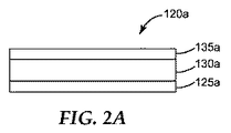
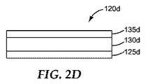
基部及びカバーは、用いられる有機化合物及び気体媒質に不透過性であり、センサ素子の電気的な行動を妨げないあらゆる固体材料を含むことができる。有用な材料の例には、ガラス及びプラスチックが挙げられる。次に図2A〜2Dを参照すると、センサ素子120a、120b、120c、120dはそれぞれ、第1の外層125a、125b、125c、125d、第2の外層135a、135b、135c、135d、及びにこれらの間にそれぞれ配置される検出層130a、130b、130c、130dを備える。
The base and cover can comprise any solid material that is impermeable to the organic compound and gaseous medium used and does not interfere with the electrical behavior of the sensor element. Examples of useful materials include glass and plastic. 2A-2D, the
検出層は、微多孔性材料を含むこと、又は微多孔性材料から本質的になる(すなわち、実質的に吸収性に影響を与えない組成物のみを含む)ことができる。対応する第1の外層又は第2の外層のそれぞれの少なくとも1つは、検出層内に容易に拡散が可能であり、センサ素子の物理パラメータ(例えば、静電容量又は反射スペクトルのピークシフト)の変化を生じさせることができるよう、未知の有機化合物に対する透過性である必要がある。 The detection layer can comprise a microporous material or consist essentially of a microporous material (ie, only comprise a composition that does not substantially affect absorbency). At least one of each of the corresponding first outer layer or second outer layer can be easily diffused into the detection layer, and the physical parameters of the sensor element (eg, capacitance or peak shift of the reflection spectrum). It must be permeable to unknown organic compounds so that changes can be made.
第1の外層及び/又は第2の外層を作製するために使用され得る材料の例としては、有機材料、無機材料(例えば、金属酸化物)、金属、合金、及び様々な混合物、並びにこれらの材料のいずれか又はすべてを含む複合材料が挙げられるが、これらに限定されない。蒸気コーティング(例えば、熱蒸気コーティング又はスパッタコーティング)された金属若しくは金属酸化物、又はこれらの組み合わせが使用されてよい。 Examples of materials that can be used to make the first outer layer and / or the second outer layer include organic materials, inorganic materials (eg, metal oxides), metals, alloys, and various mixtures, and these Examples include, but are not limited to, composite materials that include any or all of the materials. Vapor coated (eg, thermal vapor coated or sputter coated) metals or metal oxides, or combinations thereof may be used.
センサ素子(例えば、第1、第2、第3、及び参照用センサ素子)が静電容量又は相当する電気的特性を計測するように機能する実施形態では、第1の外層及び第2の外層は、電極として機能することができる十分な導電性である必要がある。このような実施形態において、第1の外層及び第2の外層は、好ましくは約107オーム/平方未満のシート抵抗を有する。例示的な導電性材料としては、アルミニウム、ニッケル、チタン、スズ、インジウムスズ酸化物、金、銀、白金、パラジウム、炭素(カーボンナノチューブを含む)、銅、クロム、及びこれらの組み合わせが挙げられる。第1の外層及び第2の外層、及びそれらの製造方法は、明細書の後半で更に詳細に説明する。 In embodiments where the sensor elements (eg, first, second, third, and reference sensor elements) function to measure capacitance or corresponding electrical characteristics, the first outer layer and the second outer layer Must be sufficiently conductive to be able to function as an electrode. In such embodiments, the first outer layer and the second outer layer preferably have a sheet resistance of less than about 10 7 ohm / square. Exemplary conductive materials include aluminum, nickel, titanium, tin, indium tin oxide, gold, silver, platinum, palladium, carbon (including carbon nanotubes), copper, chromium, and combinations thereof. The first outer layer and the second outer layer, and their manufacturing methods will be described in more detail later in the specification.
検出層は、微多孔性材料を含む。これに関連する用語、「微多孔性の」及び「微多孔質」とは、材料が、有意な量で内部が相互接続された間隙体積を有し、(例えば、吸着等温線手段によって特徴付けられる)平均孔径が、100nm未満、典型的には10nm未満であることを意味する。このような微多孔質により、有機検体の分子(存在する場合)が、材料の内部間隙体積に浸透し、内部の細孔中に定着することが可能となる。内部の細孔におけるこのような検体の存在は、例えば、誘電率及び/又は屈折率における変化等、材料の物性の変化を生じさせることができる。 The detection layer includes a microporous material. In this context, the terms “microporous” and “microporous” have a void volume in which the material is interconnected in significant amounts (eg, characterized by adsorption isotherm means). Mean) mean pore size is less than 100 nm, typically less than 10 nm. Such microporosity allows organic analyte molecules (if present) to penetrate the internal interstitial volume of the material and settle in the internal pores. The presence of such analytes in the internal pores can cause changes in material properties, such as changes in dielectric constant and / or refractive index, for example.
誘電性及び/又は光透過性を有することができる好適な微多孔性材料の例としては、微多孔性シリカ及び有機固有微多孔性ポリマー(PIM)を挙げることができる。PIMは、非効率的な結晶充填により、ナノメートルスケールの孔を有するポリマー材料である。典型的には、PIMは、剛性なリンカーによって連結したほぼ平面的な基を備える高分子であり、この剛性なリンカーは、ねじれ点を有することにより、剛性なリンカーのそれぞれに隣接したほぼ平面的な基が、非同一平面内の配向に保持される。 Examples of suitable microporous materials that can be dielectric and / or light transmissive include microporous silica and organic intrinsic microporous polymers (PIM). PIM is a polymeric material with nanometer scale pores due to inefficient crystal packing. Typically, a PIM is a polymer with substantially planar groups connected by a rigid linker, which has a torsion point so that it is substantially planar adjacent to each of the rigid linkers. Such groups are held in non-coplanar orientation.
例えば、Chemical Communications,2004,(2),pp.230〜231で、Buddらは、剛性な及び/又はねじ曲げられた単量体のビルディングブロック間に、ジベンジジオキサンリンケージを含む一連のPIMを報告している。ポリマーのこのファミリーの代表的なメンバーとしては、スキーム1(下記、nは正の整数)により表1に示される成分A(例えば、A1、A2、又はA3)と成分B(例えば、B1、B2、又はB3)との縮合によって生成されるものが挙げられる。 For example, in Chemical Communications, 2004, (2), pp. In 230-231, Budd et al. Report a series of PIMs containing dibenzidioxane linkages between rigid and / or twisted monomeric building blocks. Representative members of this family of polymers include component A (eg, A1, A2, or A3) and component B (eg, B1, B2) shown in Table 1 according to Scheme 1 (below, n is a positive integer). Or those produced by condensation with B3).

更に好適な成分A及びB、並びに得られるPIMは、当該技術分野において既知であり、例えば、BuddらのJournal of Materials Chemistry,2005,Vol.15,pp.1977〜1986;McKeownらのChemistry,A European Journal,2005,Vol.11,pp.2610〜2620;GhanemらのMacromolecules,2008,vol.41,pp.1640〜1646;GhanemらのAdvanced Materials,2008,vol.20,pp.2766〜2771;CartaらのOrganic Letters,2008,vol.10(13),pp.2641〜2643;PCT国際特許出願第2005/012397(A2)号(McKeownら)、米国特許出願第2006/0246273号(McKeownら)の中で報告されており、これらの開示は参照により本明細書に組み込まれる。 Further suitable components A and B, and the resulting PIMs are known in the art, see, eg, Budd et al., Journal of Materials Chemistry, 2005, Vol. 15, pp. 1977-1986; McKeown et al., Chemistry, A European Journal, 2005, Vol. 11, pp. 2610-2620; Ghanem et al., Macromolecules, 2008, vol. 41, pp. 1640-1646; Ghanem et al., Advanced Materials, 2008, vol. 20, pp. 2766-2771; Carta et al., Organic Letters, 2008, vol. 10 (13), pp. 2641-2643; PCT International Patent Application No. 2005/012397 (A2) (McKeown et al.), US Patent Application No. 2006/0246273 (McKeown et al.), The disclosures of which are incorporated herein by reference. Incorporated into.
そのようなポリマーは、例えば、A1(5,5’,6,6’−テトラヒドロキシ−3,3,3’,3’−テトラメチル−1,1’−スピロビスインダン)などのビス−カテコールが、塩基性条件下で、例えば、B1(テトラフルオロテレフタロニトリル)などのフッ素化アレーンと反応させられる逐次重合によって、合成することができる。得られるポリマーの主鎖の剛性及び歪んだ性質ゆえに、これらのポリマーは、固体状態で密に充填することができず、したがって、少なくとも10パーセントの自由体積を有し、本質的に微多孔性である。 Such polymers are, for example, bis-catechols such as A1 (5,5 ′, 6,6′-tetrahydroxy-3,3,3 ′, 3′-tetramethyl-1,1′-spirobisindane). Can be synthesized by sequential polymerization, for example, by reacting with a fluorinated arene such as B1 (tetrafluoroterephthalonitrile) under basic conditions. Due to the rigid and distorted nature of the resulting polymer backbone, these polymers cannot be tightly packed in the solid state and thus have at least 10 percent free volume and are essentially microporous. is there.
PIMは、他の材料にブレンドされてもよい。例えば、PIMは、それ自体が吸収性微多孔性材料ではない材料とブレンドされてもよい。検体反応に寄与しないものの、このような材料は他の理由のために有用であり得る。例えば、このような材料は、優れた機械特性などを有する、PIM含有層の形成を可能にすることがある。一部の実施形態において、PIMは、他の材料と共に一般的な溶媒に溶解して、均質な溶液を形成してもよいが、これはキャスティングされて、PIM及び他のポリマーの双方を含む吸収性誘導体ブレンド層を形成してもよい。(1つ又は複数の)PIMはまた、吸収性誘電性材料である材料(例えば、ゼオライト、活性炭、シリカゲル、超架橋ポリマーネットワークなど)とブレンドされてもよい。このような材料は、PIM材料を含む溶液中に懸濁された不溶性材料を含んでよい。 The PIM may be blended with other materials. For example, the PIM may be blended with a material that is not itself an absorbent microporous material. While not contributing to the analyte reaction, such materials may be useful for other reasons. For example, such materials may allow the formation of PIM-containing layers, such as having excellent mechanical properties. In some embodiments, the PIM may be dissolved in common solvents with other materials to form a homogeneous solution, which is cast to absorb both PIM and other polymers. A functional derivative blend layer may be formed. The PIM (s) may also be blended with a material that is an absorptive dielectric material (eg, zeolite, activated carbon, silica gel, hypercrosslinked polymer network, etc.). Such materials may include insoluble materials suspended in a solution containing PIM material.
PIMは、典型的に、例えば、テトラヒドロフランなどの有機溶媒に可溶性であり、ゆえに、溶液から(例えば、スピンコーティング、ディップコーティング、又はバーコーティングによって)フィルムとしてキャスティングすることができる。しかし、これらのポリマーの溶液から作製されるフィルムの特徴(入手可能な厚さ、光学的透明度、及び/又は外観)が、フィルムのキャスティングに使用される溶媒又は溶媒系に応じて著しく異なる場合がある。例えば、より高い分子量のPIMを、本明細書に記載のようなセンサ素子用に望ましい特性を有する膜を生成するために、あまり一般的でない溶媒(例えば、シクロヘキセンオキシド、クロロベンゼン、又はテトラヒドロピラン)からキャスティングする必要があり得る。溶液コーティング方法に加えて、検出層は、任意の他の好適な方法によって第1の外層に適用されてもよい。 PIM is typically soluble in organic solvents such as, for example, tetrahydrofuran and can therefore be cast as a film from solution (eg, by spin coating, dip coating, or bar coating). However, the characteristics (available thickness, optical clarity, and / or appearance) of films made from solutions of these polymers can vary significantly depending on the solvent or solvent system used for film casting. is there. For example, higher molecular weight PIMs can be obtained from less common solvents (eg, cyclohexene oxide, chlorobenzene, or tetrahydropyran) to produce films with desirable properties for sensor elements as described herein. It may be necessary to cast. In addition to the solution coating method, the detection layer may be applied to the first outer layer by any other suitable method.
PIMが堆積される(例えば、コーティングされる)か、ないしは別の方法で、例えば、検出層を形成するように第1の外層に形成された後、例えば、ビス(ベンゾニトリル)二塩化パラジウム(II)などの好適な架橋剤を使用して架橋することができる。このプロセスは、検出層を有機溶媒中で不溶性にするか、並びに/又は例えば、耐久性及び/若しくは摩擦耐性などのある物理的特性を向上することがあり、これはある用途において望ましい場合がある。 After PIM is deposited (eg, coated) or otherwise formed on the first outer layer, eg, to form a detection layer, for example, bis (benzonitrile) palladium dichloride ( It can be crosslinked using a suitable crosslinking agent such as II). This process may render the detection layer insoluble in organic solvents and / or improve certain physical properties such as, for example, durability and / or friction resistance, which may be desirable in certain applications. .
PIMは、材料が著しく増大するか、そうでない場合は物理的特性の顕著な変化を示す程度の液体水を吸収することがないように、疎水性であってよいが、これは必須条件ではない。このような疎水性特性は、水の存在に対する感度が比較的低いセンサ素子を準備するために有用である。 The PIM may be hydrophobic so that it does not absorb liquid water to the extent that the material increases significantly or otherwise exhibits significant changes in physical properties, but this is not a requirement. . Such hydrophobic properties are useful for preparing sensor elements that are relatively insensitive to the presence of water.
検出層は、連続マトリックスを備えてもよい。このようなマトリックスは、材料の固体部分が連続的に相互接続されているアセンブリ(例えば、コーティング及び/又は層)として定義される(上記の多孔質の存在、又は下記の任意の添加物の存在とは関わりなく)。即ち、連続的なマトリックスは、粒子の凝集(例えば、ゼオライト、活性炭、及びカーボンナノチューブ)を含むアセンブリから区別できる。例えば、溶液から堆積される層又はコーティングは、典型的には、連続的なマトリックスを含む(コーティング自体がパターンを有する方法で塗布されるか、及び/又は粒子状の添加物を含むとしても)。粉末の噴霧、分散体(例えば、ラテックス)のコーティング及び乾燥、又はゾル−ゲル混合物のコーティング及び乾燥によって堆積された粒子の集合は、連続的な網状組織を含まないことがある。しかしながら、このようなラテックス又はゾル−ゲルの層が、個別の粒子がもはや認識不可能であるか、又は異なる粒子から得られたアセンブリの領域を認識することが不可能であるように固化され得る場合に、このような層は、連続的マトリックスであると考えることができる。 The detection layer may comprise a continuous matrix. Such a matrix is defined as an assembly (eg, coatings and / or layers) in which solid portions of the material are continuously interconnected (the presence of the above-described porosity or the presence of any of the following additives) No matter what). That is, a continuous matrix can be distinguished from an assembly that includes agglomeration of particles (eg, zeolite, activated carbon, and carbon nanotubes). For example, a layer or coating deposited from a solution typically includes a continuous matrix (even though the coating itself is applied in a pattern-wise manner and / or includes particulate additives). . Aggregates of particles deposited by powder spraying, dispersion (eg, latex) coating and drying, or sol-gel mixture coating and drying may not include a continuous network. However, such a latex or sol-gel layer can be solidified such that individual particles are no longer recognizable or cannot recognize areas of the assembly obtained from different particles. In some cases, such a layer can be considered a continuous matrix.
測定した物理パラメータが、センサ素子の静電容量又は他の一部の電気的特性(例として、静電容量、インピーダンス、インダクタンス、電圧、導電率、アドミタンス、電流、抵抗、位相角、損失率、又は散逸が挙げられるが、これらに限定されない)を検出するそれらの実施形態では、検出層は、誘電性(すなわち、非導電性材料)でなければならない。微多孔性材料の空隙空間中に吸着及び/又は吸収した有機化合物が存在するために、検出層の誘電率(及び任意に厚さ)に変化が生じれば、物理パラメータに関して観測されたセンサ素子の応答も変化する。 The measured physical parameter is the capacitance of the sensor element or some other electrical characteristic (for example, capacitance, impedance, inductance, voltage, conductivity, admittance, current, resistance, phase angle, loss rate, In those embodiments that detect (or include but are not limited to) dissipation, the detection layer must be dielectric (ie, non-conductive material). Sensor element observed with respect to physical parameters if there is a change in the dielectric constant (and optionally thickness) of the detection layer due to the presence of adsorbed and / or absorbed organic compounds in the void space of the microporous material The response also changes.
このような測定可能な変化が、第1の外層及び第2の外層(本実施形態ではそれぞれ第1の電極及び第2の電極として機能する)と電気的に導通する動作回路によって検出されてもよい。これに関連して「動作回路」とは、一般に、第1の外層及び第2の外層に電圧を印加する(したがって、電極に電荷差を付与する)、及び/又はセンサ素子の電気的特性(電気的特性は有機検体の存在に反応して変化し得る)をモニタするために使用され得る電気装置を指す。動作回路の例として、マルチメータ及びコンピュータが挙げられる。 Even if such a measurable change is detected by an operating circuit that is in electrical communication with the first outer layer and the second outer layer (functioning as the first electrode and the second electrode, respectively in this embodiment). Good. In this context, an “operational circuit” generally refers to applying a voltage to the first outer layer and the second outer layer (thus providing a charge difference to the electrodes) and / or electrical characteristics of the sensor element ( An electrical property refers to an electrical device that can be used to monitor (which can change in response to the presence of an organic analyte). Examples of the operating circuit include a multimeter and a computer.
任意に、第1の外層が基部上に配置されてもよい。センサ素子の機能を妨げないように、基部を選択する必要がある。基部は、センサ素子の構成に応じて、導電性でも非導電性でもよく、例えば、第1の外層が導電性であるセンサ素子の設計に対し、基部は、非導電性(例えば、誘電性)としてもよい。好適な基部の例としては、プラスチック薄膜(例えば、ポリエステル、ポリカーボネート、及びポリオレフィンフィルム)、ガラス、及びセラミックを挙げることができる。本開示の実施において有用なセンサ素子を作製するための例示的なプロセスでは、(材料の連続的なスラブ、層又はフィルムであり得る)誘電性の基部が提供されるが、これは、第1電極に近接し、完成したセンサ素子に物理的強度、及び一体性を提供するように機能し得る。例えば、ガラス、セラミック、及び/又はプラスチックを含む、任意の好適な材料が使用されてもよい。大規模生産では、ポリマーフィルム(ポリエステルなど)が使用されてもよい。一部の実施形態において、誘電性の基部は、検体透過性材料(例えば、シリコーンゴム又は微多孔性膜)である。 Optionally, a first outer layer may be disposed on the base. The base must be selected so as not to interfere with the function of the sensor element. The base may be conductive or non-conductive depending on the configuration of the sensor element. For example, for a sensor element design where the first outer layer is conductive, the base is non-conductive (eg, dielectric). It is good. Examples of suitable bases include plastic thin films (eg, polyester, polycarbonate, and polyolefin films), glass, and ceramic. An exemplary process for making sensor elements useful in the practice of the present disclosure provides a dielectric base (which may be a continuous slab, layer or film of material), which is the first Proximate to the electrode, it can function to provide physical strength and integrity to the finished sensor element. Any suitable material may be used including, for example, glass, ceramic, and / or plastic. For large scale production, polymer films (such as polyester) may be used. In some embodiments, the dielectric base is an analyte permeable material (eg, silicone rubber or a microporous membrane).
一部の実施形態において、第1の外層と検出層とは、間に介在層を有することなく、直接接触する。同様に、一部の実施形態において、第2の外層と検出層とが、間に介在層を有することなく、直接接触する。しかし、他の任意の層が、第1の外層と検出層との間に、及び/又は第2の外層と検出層との間に、存在してもよいことも想定される。そのような場合、第1の外層及び第2の外層の一方又は両方の少なくとも一部が検出層の一部又は全てと直接接触しないようにしてもよい。例えば、電極と検出層との間の結合を向上させるために、1つ又は複数の結合層が使用されてよい。又は、電極間のアーク放電の可能性を最小限に抑えるために、不動態層(例えば、二酸化ケイ素の層)が、検出層の表面と電極表面との間に置かれてもよい。一部の実施形態において、複数のこのような任意の層が使用され得、あるいは、単一の層が複数の機能を果たし得る。いずれかのこのような任意の層、例えば、上記の結合層、不動態層、保護層、及びカバー層などは、センサ素子の所望の機能を有意に妨げない限り、あらゆる目的のために使用され得る。例えば、有機化合物が検出層に到達するために、任意の層を通過しなくてはならないようにセンサ素子が構成されている場合に、任意の層は、対象の有機化合物に対して十分に透過性であるべきである。 In some embodiments, the first outer layer and the detection layer are in direct contact with no intervening layer in between. Similarly, in some embodiments, the second outer layer and the detection layer are in direct contact with no intervening layer in between. However, it is envisioned that any other layer may be present between the first outer layer and the detection layer and / or between the second outer layer and the detection layer. In such a case, at least part of one or both of the first outer layer and the second outer layer may not be in direct contact with part or all of the detection layer. For example, one or more binding layers may be used to improve the coupling between the electrode and the detection layer. Alternatively, a passivating layer (eg, a layer of silicon dioxide) may be placed between the surface of the detection layer and the electrode surface to minimize the possibility of arcing between the electrodes. In some embodiments, multiple such optional layers may be used, or a single layer may serve multiple functions. Any such optional layers, such as the tie layers, passive layers, protective layers, and cover layers described above, can be used for any purpose, as long as they do not significantly interfere with the desired function of the sensor element. obtain. For example, if a sensor element is configured such that an organic compound must pass through an arbitrary layer in order to reach the detection layer, the arbitrary layer is sufficiently permeable to the target organic compound. Should be sex.
一般に、第1の外層及び/又は第2の外層及び/又は検出層の端部は、互いにぴったり重なっていてよく、あるいは、互いに関連して若しくは存在し得る任意の他の層に関連して、後ろにあっても、及び/又は延在していてもよい。 In general, the ends of the first outer layer and / or the second outer layer and / or the detection layer may be flush with each other, or in relation to each other or any other layer that may be present, It may be behind and / or extend.
第1の外層上への検出層の堆積の間、動作回路との電気的な接触を可能にするため、電気的にアクセス可能な領域が第1の外層上に設けられてよい。同様に、カバー層が第2の外層上に置かれる場合、電気的にアクセス可能な領域が同様に設けられてよい。このような電気的にアクセス可能な領域は、任意の便利な位置に設けられてよい。一部の実施形態において、接続装置(例えば、接触パッド、タブなど)は、第1の外層のアクセス可能な領域と電気的に接触させて置かれてもよい。同様に、接続装置は、第2の外層のアクセス可能な領域と同様に接触させて置かれてもよい。 An electrically accessible region may be provided on the first outer layer to allow electrical contact with the operating circuit during the deposition of the detection layer on the first outer layer. Similarly, if the cover layer is placed on the second outer layer, an electrically accessible area may be provided as well. Such an electrically accessible area may be provided at any convenient location. In some embodiments, a connection device (eg, contact pads, tabs, etc.) may be placed in electrical contact with an accessible area of the first outer layer. Similarly, the connecting device may be placed in contact as well as the accessible area of the second outer layer.
センサ素子の性能の改良は、一般的に、有機化合物への曝露の前にセンサ素子を加熱すること、例えば、第2の外層の堆積後、100℃〜250℃の温度に、第1の外層を、典型的にはセンサ素子の他の成分と共に、(例えば、抵抗加熱により又は外部の加熱要素を用いて)加熱することにより、実現することができる。これらの温度における均熱時間は任意の持続時間を有してよいが、典型的には、数分〜数時間の範囲である。 Improvements in sensor element performance generally include heating the sensor element prior to exposure to the organic compound, eg, after deposition of the second outer layer, to a temperature between 100 ° C. and 250 ° C. Can be achieved by heating, typically with other components of the sensor element (eg, by resistive heating or using an external heating element). The soaking time at these temperatures may have any duration, but typically ranges from a few minutes to a few hours.
一部の実施形態において、第1の外層が任意の基板上に設けられる。導電性層は、導電性及び非導電性材料のブレンド又は混合物を包含する、上記の材料のいずれかを含んでもよく、スピンコーティング、ディップコーティング、スクリーン印刷、トランスファーコーティング、スパッタコーティング、物理蒸着、化学蒸着、又はこれらの方法の2つ以上の組み合わせが挙げられるが、これらに限定されない任意の好適な方法によって堆積され得る。別の実施形態において、導電性層は、誘電性基板の上に予め作製されたフィルム(例えば、金属フォイル、導電性テープなど)を置くことによって設けられてよい。この第1の外層は、前述されるように、連続的な層として又は非連続的な層として提供され得る。 In some embodiments, a first outer layer is provided on any substrate. The conductive layer may include any of the above materials, including blends or mixtures of conductive and non-conductive materials, such as spin coating, dip coating, screen printing, transfer coating, sputter coating, physical vapor deposition, chemical It may be deposited by any suitable method including, but not limited to, vapor deposition, or a combination of two or more of these methods. In another embodiment, the conductive layer may be provided by placing a prefabricated film (eg, metal foil, conductive tape, etc.) on the dielectric substrate. This first outer layer can be provided as a continuous layer or as a non-continuous layer, as described above.
一部の実施形態において、第1の外層は、任意の基板の少なくとも一部に、近接して及び/又は接触して配置される。別の実施形態では、第1の外層の少なくとも一部と任意の基板との間に、任意の層が存在してもよい。この任意の層は、この層がセンサ素子の機能を妨げない限り、任意の目的(例えば、第1の外層と基板との結合の向上)のために用いられてよい。 In some embodiments, the first outer layer is disposed proximate and / or in contact with at least a portion of any substrate. In other embodiments, there may be an optional layer between at least a portion of the first outer layer and the optional substrate. This optional layer may be used for any purpose (eg, improved bonding between the first outer layer and the substrate) as long as this layer does not interfere with the function of the sensor element.
電気的特性(例えば、静電容量)を計測するように構成されるセンサ素子の構成に対して、導電性部材(例えば、ワイヤリード線又はトレース)を、センサ素子の組立中に、第1の外層及び第2の外層に、適切な点で電気的に結合してよい。例えば、第1の外層の堆積後及び検出の堆積の前に、直ちに、第1の導電性部材が第1の外層に結合されてよい。代替的実施形態では、第1の外層のある領域が、第1の導電性部材に結合するために露出したままになるよう、検出層が第1の外層上に堆積されてよい。同様に、第2の導電性部材は、第2の外層の堆積の直後及び任意のカバー層の堆積前に、第2の外層に結合されてよく、あるいは任意のカバー層は、第2の外層のある領域が、第2の導電性部材に結合されるために露出されたままになるように、第2の外層上に堆積されてよい。 For a sensor element configuration configured to measure electrical characteristics (eg, capacitance), a conductive member (eg, wire lead or trace) may be applied to the first during assembly of the sensor element. The outer layer and the second outer layer may be electrically coupled at appropriate points. For example, a first conductive member may be coupled to the first outer layer immediately after deposition of the first outer layer and prior to detection deposition. In an alternative embodiment, a detection layer may be deposited on the first outer layer such that a region of the first outer layer remains exposed for coupling to the first conductive member. Similarly, the second conductive member may be coupled to the second outer layer immediately after deposition of the second outer layer and before deposition of the optional cover layer, or the optional cover layer may be coupled to the second outer layer. A certain region of may be deposited on the second outer layer such that it remains exposed for coupling to the second conductive member.
一部の実施形態において、例えば、溶媒コーティング、スピンコーティング、ディップコーティング、トランスファーコーティング、及び/又はスクリーン印刷を含むコーティングプロセスにより、微多孔性材料は、第1の外層に近接して置かれてもよい。ある実施形態において、誘電性材料は、センサ素子の性能を損なうように作用し得る、欠陥、ピンホールなどの存在を最小限に抑えるような方法で堆積される。特定の実施形態では、検出層は、PIMを含む溶液を好適な基板上にコーティングし、溶液を乾燥させて、PIM材料を含む固体層を形成することによって堆積される、固有微多孔性(PIM)ポリマーを含む。所望により、この構成体を100℃〜200℃の範囲の温度で加熱して、コーティングされたPIM材料を更に乾燥させてよい。 In some embodiments, the microporous material may be placed in proximity to the first outer layer by a coating process including, for example, solvent coating, spin coating, dip coating, transfer coating, and / or screen printing. Good. In certain embodiments, the dielectric material is deposited in a manner that minimizes the presence of defects, pinholes, etc. that may act to compromise the performance of the sensor element. In certain embodiments, the detection layer is deposited by coating a solution containing PIM onto a suitable substrate and drying the solution to form a solid layer containing PIM material (PIM). ) Including polymers. If desired, the construct may be heated at a temperature in the range of 100 ° C. to 200 ° C. to further dry the coated PIM material.
また、検出層は、他の方法で提供することもできる。例えば、微多孔性材料が予め形成されたフィルムを、第1の外層に置かれてもよい。別の実施形態において、吸収性誘電性材料は、粒状形態(例えば、粉末として、懸濁液として、又はゾルとして)で提供され、このような形態で第1の外層上に堆積して、粒状コーティングを形成することができる。必要に応じて、このような材料は、吸収性誘電性材料の連続的なマトリックスを形成するように固化され得る。 The detection layer can also be provided by other methods. For example, a film pre-formed with a microporous material may be placed on the first outer layer. In another embodiment, the absorbent dielectric material is provided in a particulate form (eg, as a powder, as a suspension, or as a sol) and deposited in such form on the first outer layer to form a particulate A coating can be formed. If desired, such materials can be solidified to form a continuous matrix of absorbent dielectric material.
任意の保護カバー又はバリア層が、第2の外層に近接して提供されてもよい。例えば、一部の実施形態において、カバー層を第2の外層上に置き、第2の外層のある領域を、例えば、導電性部材による電気的な接触に対してアクセス可能としたままにすることもできる。好ましくは、いかなるこのようなカバー層も、センサ素子の機能を有意に妨げるべきではない。例えば、センサ素子が、対象の検体が検出層に到達するためにカバー層を通過しなくてはならないように構成されている場合、カバー層は、対象の有機化合物に対して十分に透過性でなければならない。 An optional protective cover or barrier layer may be provided proximate to the second outer layer. For example, in some embodiments, the cover layer is placed on the second outer layer, and certain areas of the second outer layer remain accessible for electrical contact, eg, with a conductive member. You can also. Preferably, any such cover layer should not significantly interfere with the function of the sensor element. For example, if the sensor element is configured so that the analyte of interest must pass through the cover layer in order to reach the detection layer, the cover layer is sufficiently permeable to the organic compound of interest. There must be.
任意のカバー層は、コーティング(例えば、スピンコーティング、ディップコーティング、溶媒コーティング、蒸気コーティング、トランスファーコーティング、スクリーン印刷、フレキソ印刷など)を含む、当該技術分野において既知の任意の方法で堆積されてよい。別の実施形態において、カバー層は、予め作製した層(例えば、フィルム又はテープ)を含むことができ、これは第2の外層上に置かれる。任意のカバー層は、第2の外層の主表面の少なくとも一部と直接接触するように設けられてよい。カバー層は、センサ素子の最も外層であってよく、又はそれ自体が必要に応じて追加のコーティング又は層を受容してよい。 The optional cover layer may be deposited by any method known in the art, including coating (eg, spin coating, dip coating, solvent coating, vapor coating, transfer coating, screen printing, flexographic printing, etc.). In another embodiment, the cover layer can include a prefabricated layer (eg, a film or tape) that is placed on the second outer layer. An optional cover layer may be provided in direct contact with at least a portion of the major surface of the second outer layer. The cover layer may be the outermost layer of the sensor element, or itself may receive additional coatings or layers as needed.
一部の実施形態において、検出層の少なくとも1つにより、有機化合物が十分に吸着/吸収されることで、センサ素子に関連する電気的特性(例として、静電容量、インピーダンス、インダクタンス、アドミタンス、電流、又は抵抗が挙げられるが、これらには限定されない)における検出可能な変化が生じ得る。このような検出可能な変化は、第1の外層及び第2の外層と電気的に導通する動作回路によって検出され得る。これに関連して「動作回路」とは、一般に、第1の外層及び第2の外層に電圧を印加する(したがって、電極に電荷差を付与する)ために、及び/又はセンサ素子の電気的特性(電気的特性は有機検体の存在に反応して変化し得る)をモニタするために使用され得る電気装置を指す。このような動作回路は、第1の外層及び第2の外層の両方へ電圧を印加し、電気的特性をモニタする1つの装置を備えてもよい。別の実施形態では、このような動作回路は、電圧を提供するものと、信号をモニタするものとの2つの別個の装置を含んでもよい。動作回路は、典型的には、導電性部材によって、第1の外層及び第2の外層に電気的に結合されている。 In some embodiments, at least one of the detection layers sufficiently adsorbs / absorbs the organic compound so that electrical characteristics associated with the sensor element (eg, capacitance, impedance, inductance, admittance, There can be a detectable change in current, or resistance, including but not limited to. Such a detectable change can be detected by an operating circuit that is in electrical communication with the first outer layer and the second outer layer. In this context, an “operational circuit” generally refers to applying a voltage to the first outer layer and the second outer layer (and thus providing a charge difference to the electrodes) and / or the electrical of the sensor element. Refers to an electrical device that can be used to monitor properties (electrical properties can change in response to the presence of an organic analyte). Such an operating circuit may comprise a single device that applies a voltage to both the first outer layer and the second outer layer and monitors the electrical characteristics. In another embodiment, such an operating circuit may include two separate devices, one that provides the voltage and one that monitors the signal. The operating circuit is typically electrically coupled to the first outer layer and the second outer layer by a conductive member.
図1及び図3において、気体媒質115を未知の有機化合物110と組み合わせて、雰囲気サンプル102を生成する。
1 and 3, the
図1に示される実施形態では、センサ素子120a、120b、120c、120dが、電気的特性を検出するように構成される(例えば、静電容量ベースのセンサ素子)。本実施形態では、各センサ素子120a、120b、120c、120dの各第1の外層及び各第2の外層125a、135a、125b、135b、125c、135c、125d、135dは、導電性である。動作回路130は、導電性部材(132a、132b、134a、134b、136a、136b、138a、138b)を介して、センサ素子120a、120b、120c、120dと電気的に導通する。電源に接続すれば、動作回路は、センサ素子の静電容量(又は他の所望の電気的特性)を計測する。
In the embodiment shown in FIG. 1,
動作回路は、データ記憶装置、コンピュータプロセッサ、プロセスコントローラ装置、及び/又はディスプレイ装置の1つ以上と通信結合されてもよい。動作中、動作回路は、電源と電気的に導通する。例示の電源としては、電池、プラグイン電源、発電機、配線接続された電源、及び高周波(RF)発生機(動作回路に、RFレシーバーが含まれている場合)が挙げられる例示のディスプレイ装置としては、発光ダイオード(LED)ディスプレイ、液晶ディスプレイ(LCD)、CRT(CRT)ディスプレイ、直流メータ、及びプリンタが挙げられる。コントローラ装置が存在する場合、これには、動作回路の動作を指示するハードウェア及び/又はソフトウェアが含まれる。例示のデータ記憶装置としては、フラッシュメモリ装置、ハードディスク、デジタルテープ、CD Rメディア、及びCD RWメディアが挙げられる。 The operating circuit may be communicatively coupled to one or more of a data storage device, a computer processor, a process controller device, and / or a display device. During operation, the operating circuit is in electrical communication with the power source. Exemplary power supplies include batteries, plug-in power supplies, generators, wired power supplies, and radio frequency (RF) generators (if the operating circuit includes an RF receiver) as exemplary display devices Include light emitting diode (LED) displays, liquid crystal displays (LCD), CRT (CRT) displays, DC meters, and printers. If a controller device is present, this includes hardware and / or software that directs the operation of the operating circuit. Exemplary data storage devices include flash memory devices, hard disks, digital tapes, CDR media, and CD RW media.
別の実施形態では、動作回路は、接続部材によって、又は動作回路の一部分を各電極の電気的にアクセス可能な領域に直接接触させることによって、のいずれかで、第1の外層及び/又は第2の外層のそれぞれと直接接触するように設けられてよい。例えば、回路基板上、又はフレキシブル回路上(これらのいずれかは、誘電性基板としても機能し得る)に存在する動作回路が設けられ得る。第1の外層は次に、動作回路の一部と直接的に接触するように、誘電性基板上に直接堆積され得る。 In another embodiment, the operating circuit is either connected to the first outer layer and / or the first outer layer either by a connecting member or by directly contacting a portion of the operating circuit to the electrically accessible area of each electrode. It may be provided in direct contact with each of the two outer layers. For example, an operating circuit may be provided that exists on a circuit board or a flexible circuit, either of which can also function as a dielectric substrate. The first outer layer can then be deposited directly on the dielectric substrate so as to be in direct contact with a portion of the operating circuit.
次に図3を参照すると、本開示を行うために好適な例示の光化学センサ装置300は、(雰囲気サンプルを受容するための)入口開口322a及び(雰囲気サンプルの気体媒質に対応する参照用ガスを受容するための)入口開口322bを有しているディスペンサーチャネル305と、それぞれのセンサ素子320a、320b、320c、320dに独立に流体連通する複数の出口開口324a、324b、324c、324dと、を含む。センサ素子320a、320b、320c、320dは、光を反射するように構成され、独立に作動するよう、壁340a、340b、340c、340d、340e、基部360、及びカバー355によって形成されるそれぞれ隔離されたセンサチャンバ370a、370b、370c、370dの中に配置される。本実施形態では、基部及びカバーは、用いられる有機化合物及び気体媒質に対して不透過性で及びセンサ素子から光を反射する能力を全体的に妨げない、任意の固体成分を含むことができる。有用な材料の例として、金属、ガラス、及びプラスチックが挙げられる。
Referring now to FIG. 3, an exemplary
センサ素子320a、320b、320c、320dは、各ディスペンサーチャネル305の出口開口324a、324b、324c、324dと流体連通する。センサ素子320a、320b、320c、320dを有機化合物の蒸気に曝露すれば、検出層130a、130b、130c、130dが、未知の有機化合物の少なくとも一部を吸着/吸収し、屈折率及び/又はセンサ素子の厚さが変化し、これに応じてセンサ素子の第2の外層上に入射する光の反射スペクトル(例えば、光化学センサ素子)も変化する。
次に図4A〜4Dを参照すると、センサ素子320a、320b、320c、320dは、少なくとも一部がそれぞれ反射性の第1の外層305a、305b、305c、305dと、それぞれ半反射性の第2の外層315a、315b、315c、315dと、を含む。「半反射性の第2の外層」とは、それぞれの第2の外層が、300ナノメートル(nm)〜2500nmの波長範囲にわたって、典型的には300nm〜1100nmの波長範囲にわたって、(例えば、少なくとも20、30、40、又は50パーセントの)一部の入射光を反射し、(例えば、少なくとも20、30、40、又は50パーセントの)一部の入射光を透過する。本実施形態では、第1の外層は、高反射性(例えば、50、60、70、80、又は更に少なくとも90パーセント)であることが好ましい。第1の外層は、典型的には、半反射性の第2の外層よりも高い反射性(例えば、少なくとも50、60、70、80、90、95、又は更に少なくとも99パーセントの反射性)を有するように作製されるが、一部の実施形態において、第1の外層及び第2の外層が実質的に同じ反射性を有することが望ましい場合もある。別の実施形態では(図示せず)、比較的高い反射性を有するように第2の外層を作製すること、及び第1の外層の反射性を低減して半反射性とすることができ、そのため、例えば、任意の基板を用いて反射率測定を行うことができる。
4A-4D, the
一部の実施形態において、50〜500nmの厚さに堆積される銀又は金のナノ粒子からなる導電性インクを用いて、反射性でありながら有機化合物に対する透過性も保持する外層(例えば、第2の外層)を作製することができる。 In some embodiments, an outer layer (e.g., a first layer) that is reflective but retains permeability to organic compounds using a conductive ink composed of silver or gold nanoparticles deposited to a thickness of 50-500 nm. 2 outer layers) can be produced.
光化学センサ素子の場合、第1の外層及び第2の外層は、(例えば、静電容量センサの事例の場合のように)導電性である必要はない。従って、それらは所望の反射性を有する全ての材料で作製されてよい。本実施形態における第1の外層及び第2の外層の厚さは、典型的には、透明性に影響し(例えば、厚さが増せば透明性が低くなる)、薄過ぎる場合(例えば、用いる入射光の波長の4分の1未満)は反射性に悪影響を及ぼし得る。 In the case of a photochemical sensor element, the first outer layer and the second outer layer need not be electrically conductive (eg, as in the case of a capacitive sensor). Thus, they may be made of any material that has the desired reflectivity. The thicknesses of the first outer layer and the second outer layer in this embodiment typically affect transparency (eg, increasing thickness reduces transparency) and are too thin (eg, used) Less than a quarter of the wavelength of the incident light) can adversely affect reflectivity.
再び、図3を参照すると、光源380a、380b、380c、380d(例えば、タングステン電球、キセノンランプ、発光ダイオード(LED)、及び/又は少なくとも1つのレーザー)からセンサ素子に入射する光線350a、350b、350c、350dは、各センサ素子の第1の外層及び第2の外層の両者に反射されて、反射光の各スペクトル(すなわち、反射スペクトル)における変化として現れる干渉効果が得られ、この効果は、光検出器330a、330b、330c、330d(例えば、分光光度計及び/又はフォトダイオード)を介して検出される。複数の光源の代わりに、単一光源を用いることができることも考慮される。
Referring again to FIG. 3,
典型的に、入射光は300〜2500nmの範囲の1つ以上の波長を含む。光源が放射する光は、広帯域(例えば、白色光)、又は狭帯域(例えば、LED又はレーザー光)であってよい。センサ素子から反射される光の特性は、様々な層(例えば、反射導電性電極及び半反射導電性電極)、及びセンサ素子の他の界面から反射した光の干渉からもたらされる。このような反射光は、1つ以上のスペクトル特性(例えば、頂点、底点、及び/又は変曲点)を持つ反射スペクトルを有する。(1つ又は複数の)スペクトル特性の大きさ及び/又は位置は、検体の存在に応じて変化する。1つ以上の波長の頂点の位置及び大きさが変化した場合(即ち、検体濃度の変化による)、光検出器が検出する反射光の量、スペクトル分布、又は強度は変化し得る。 Typically, the incident light includes one or more wavelengths in the range of 300-2500 nm. The light emitted by the light source may be broadband (eg, white light) or narrow band (eg, LED or laser light). The property of light reflected from the sensor element results from interference of light reflected from various layers (eg, reflective and semi-reflective conductive electrodes) and other interfaces of the sensor element. Such reflected light has a reflected spectrum with one or more spectral characteristics (eg, apex, base, and / or inflection point). The magnitude and / or position of the spectral characteristic (s) will vary depending on the presence of the analyte. When the position and size of one or more wavelength vertices change (ie, due to changes in analyte concentration), the amount of reflected light, spectral distribution, or intensity detected by the photodetector may change.
反射光を、反射波長の最大帯域シフトを測定可能な光検出器を使用して分析する。反射波長の最大帯域シフトは、例えば、反射の最小点(底点)、最大点(頂点)、又は変曲点で波長が変化するため、容易に得ることができる。静電容量と同様に、スペクトル変化は、検体の存在しない同一条件(例えば、温度及び湿度)の下で観察される基準反射スペクトルに関連して決定される。 The reflected light is analyzed using a photodetector that can measure the maximum band shift of the reflected wavelength. The maximum band shift of the reflection wavelength can be easily obtained, for example, because the wavelength changes at the minimum point (bottom point), maximum point (vertex point), or inflection point of reflection. Similar to capacitance, the spectral change is determined relative to the reference reflectance spectrum observed under the same conditions (eg, temperature and humidity) in the absence of the analyte.
光検出器は、(例えば、上の図3に示される実施形態に関して記述されるように)データ記憶装置、コンピュータプロセッサ、プロセスコントローラ装置、及び/又はディスプレイ装置の1つ以上と通信結合される。 The photodetector is communicatively coupled to one or more of a data storage device, a computer processor, a process controller device, and / or a display device (eg, as described with respect to the embodiment shown in FIG. 3 above).
光化学測定技術及び同装置に関する詳細は、米国特許第7,556,774号(Rakowら)及び同第7,906,233号(Rakowら)、米国特許出願公開公報第2010/277740(A1)号(Rakowら)、及び2011年4月13日に提出の米国仮特許出願第61/475000号、表題「METHOD OF DETECTING VOLATILE ORGANIC COMPOUNDS」に記載され、これらの開示内容は参照として本願に組み込まれる。 Details regarding the photochemical measurement technique and the apparatus are described in US Pat. Nos. 7,556,774 (Rakow et al.) And 7,906,233 (Rakow et al.), US Patent Application Publication No. 2010/277740 (A1). (Rakow et al.), And US Provisional Patent Application No. 61/475000 filed Apr. 13, 2011, entitled “METHOD OF DETECTING VOLATILE ORGANIC COMPOUNDS”, the disclosures of which are incorporated herein by reference.
前述のセンサ素子の構成(例えば、静電容量又は光化学)が実装されることには関係無く、第2の外層(及び任意に第1の外層)は、未知の有機化合物に対して透過性であることが好ましい。多孔性の導電性及び/又は半反射性の第2の外層の例としては、例えば、銅、シリコン、アルミニウム、ロジウム、イリジウム、ニッケル、クロム、オスミウム、金、銀、パラジウム、又はこれらの組み合わせといった金属類を含む熱蒸着金属フィルムが挙げられる。原理上は、(上述の通り、センサの設計に応じて)十分な導電性及び/又は反射特性を有する限りにおいて、並びに第1の外層及び/又は第2の外層が、気体媒質中の有機化合物が検出層内に拡散できるように、これに対して十分な多孔性を有する限りにおいて、第2の外層は、どのような厚さであってもよい。典型的には、これらの特性は厚さ1nm〜50nm、より典型的には1nm〜10nm、更により典型的には4nm〜8nmで達成されるが、他の厚さであってもよい。厚さが大きい場合、一般的に、望ましくない低レベルの透過性を有する一方、厚さが小さい場合、導電性が不十分となるか、及び/又は第2導電性部材への電気的接続が困難となる。所望の厚さは、典型的には、第1の外層を形成するために用いられる材料、第1の外層及び第2の外層が堆積される材料、検出される有機化合物、及び気体媒質に依存する。 Regardless of the implementation of the sensor element configuration described above (eg, capacitance or photochemistry), the second outer layer (and optionally the first outer layer) is permeable to unknown organic compounds. Preferably there is. Examples of a porous conductive and / or semi-reflective second outer layer include, for example, copper, silicon, aluminum, rhodium, iridium, nickel, chromium, osmium, gold, silver, palladium, or combinations thereof Examples include a thermally vapor-deposited metal film containing metals. In principle, as long as it has sufficient conductivity and / or reflection properties (as described above, depending on the sensor design) and the first outer layer and / or the second outer layer are organic compounds in the gaseous medium The second outer layer can be of any thickness as long as it has sufficient porosity to allow diffusion into the detection layer. Typically, these properties are achieved with a thickness of 1 nm to 50 nm, more typically 1 nm to 10 nm, and even more typically 4 nm to 8 nm, although other thicknesses may be used. Large thicknesses generally have an undesirably low level of permeability, while small thicknesses result in poor conductivity and / or electrical connection to the second conductive member. It becomes difficult. The desired thickness typically depends on the material used to form the first outer layer, the material on which the first and second outer layers are deposited, the organic compound to be detected, and the gaseous medium. To do.
例示的な実施形態では、第2の外層は、少なくとも1つの貴金属を含む。一部の実施形態において、第2の外層は、少なくとも50、60、70、80、90、95、99、又は更に少なくとも99.9重量パーセントの貴金属含有量を有してよい。一部の実施形態において、第2の外層は、金、パラジウム、白金、又はこれらの組み合わせからなるか、又は本質的になる。第2の外層は、対象の有機化合物による透過性を維持できる限りにおいて、付加的な成分を含んでもよい。十分な全体導電性及び/又は反射性及び透過性がもたらされる限り、異なる材料(導電性及び/又は非導電性)の組み合わせが、異なる層又は混合物として使用され得る。 In an exemplary embodiment, the second outer layer includes at least one noble metal. In some embodiments, the second outer layer may have a noble metal content of at least 50, 60, 70, 80, 90, 95, 99, or even at least 99.9 weight percent. In some embodiments, the second outer layer consists or consists essentially of gold, palladium, platinum, or a combination thereof. The second outer layer may contain an additional component as long as the permeability by the target organic compound can be maintained. A combination of different materials (conductive and / or non-conductive) can be used as different layers or mixtures as long as sufficient overall conductivity and / or reflectivity and transparency are provided.
一部の実施形態において、第2の外層は、熱蒸着プロセスによって調製することができる。熱蒸着では、第2の電極の作製に用いられる材料が、気化し、感知素子の適切な構成要素(例えば、検出層又は任意のカバー層)の上に蒸着するまで、真空下で加熱される。任意の好適な加熱源が用いられてよい。例えば、抵抗加熱、レーザー加熱、及び電子ビーム加熱(電子ビーム蒸発とも呼ばれる)が挙げられる。熱蒸着は、一般的に、約10−5トル(1mPa)、10−6トル(0.1mPa)、又はそれ以下の圧力で実行される。熱蒸着とスパッタ蒸着とは異なる。スパッタ蒸着では、高エネルギー原子をターゲット又はソースに衝突させ、基材に蒸着する材料を放出させる。スパッタ蒸着に関与する典型的な圧力は、10−2トル(1Pa)〜10−4トル(0.1Pa)以上の範囲である。 In some embodiments, the second outer layer can be prepared by a thermal evaporation process. In thermal evaporation, the material used to make the second electrode is heated under vacuum until it vaporizes and deposits on the appropriate component of the sensing element (eg, the detection layer or optional cover layer). . Any suitable heating source may be used. Examples include resistance heating, laser heating, and electron beam heating (also called electron beam evaporation). Thermal evaporation is generally performed at a pressure of about 10-5 Torr (1 mPa), 10-6 Torr (0.1 mPa), or less. Thermal evaporation and sputter deposition are different. In sputter deposition, high energy atoms are bombarded by a target or source and the material deposited on the substrate is released. Typical pressures involved in sputter deposition are in the range of 10 −2 Torr (1 Pa) to 10 −4 Torr (0.1 Pa) or higher.
一部の実施形態において、第1の外層及び/又は第2の外層は、検体が検出層に侵入できる穴又は他の開いた領域を作り出すようにエッチング又は穿孔されてもよいが、これは、必要条件ではない。このような実施形態では、検出層の物理的厚さは、150nm〜1200nmの範囲、例えば500nm〜900nmの範囲であってもよいが、より薄い検出層及びより厚い検出層も使用することができる。 In some embodiments, the first outer layer and / or the second outer layer may be etched or perforated to create holes or other open areas through which the analyte can enter the detection layer, It is not a requirement. In such embodiments, the physical thickness of the detection layer may be in the range of 150 nm to 1200 nm, for example in the range of 500 nm to 900 nm, although thinner and thicker detection layers can also be used. .
1よりも大きい(例えば、2よりも大きい、3よりも大きい、4よりも大きい、5よりも大きい、10よりも大きい、又は更に20よりも大きい)個数のセンサ素子が、本開示の実施に用いられてもよい。第1、第2、第3などのセンサ素子を、独立に(直列に又は並列に)動作させてもよく、また別々の装置に位置づけてもよい。 A number of sensor elements greater than 1 (e.g., greater than 2, greater than 3, greater than 4, greater than 5, greater than 10, or even greater than 20) can be used to implement the present disclosure. May be used. The first, second, third, etc. sensor elements may be operated independently (in series or in parallel) or may be located in separate devices.
有利なことに、本開示で用いるセンサ素子は、単一装置内に配置され、雰囲気サンプルに基づく(すなわち、雰囲気サンプル由来の)未知の有機化合物の所定の希釈物を供給することができるディスペンサーに接続されてもよい。 Advantageously, the sensor element used in the present disclosure is disposed in a single device and dispenser capable of supplying a predetermined dilution of an unknown organic compound based on an atmospheric sample (ie, derived from an atmospheric sample). It may be connected.
そのような設計は、図1に示され、そこでは、ディスペンサーチャネル105が雰囲気サンプル102を受容し、それを2つの部分104、106に分割する。部分106は、未知の有機化合物を効果的に取り除き(例えば、雰囲気サンプルからの未知の有機化合物の少なくとも95パーセント、好ましくは少なくとも99パーセント、更に好ましくは少なくとも99.99パーセントを取り除き)、任意には、存在し得るあらゆる水蒸気を効果的に取り除く、少なくとも1つの多孔性フィルタ112(例えば、活性炭フィルタ)を通過し、結果的に精製部分107となる。好適な多孔性フィルタの例として、活性炭フィルタ及び多孔性の乾燥剤フィルタが挙げられる。次いで、部分104及び精製部分107は、出口開口124a、124b、124c、124dと流体連通するフローチャネル118の分岐ネットワークを介して再結合される。
Such a design is shown in FIG. 1, where the
図1に示されるセンサ素子120dは、雰囲気サンプル中の有機材料を受容せず、本開示の実施のために必要ではないが、例えば、多孔性フィルタ112が実用寿命に到達したことを判別するために有用な場合があることに留意すべきである。同様に、図3に示されるセンサ素子320dは、雰囲気サンプル中の有機材料を受容せず、本開示の実施のために必要ではないものの、実験変数、例えば、迷光が変化したことを判別するために有用な場合がある。
The
ディスペンサーチャネル105が図1に示されているが、例えば、図3に示す構成と、305として示すディスペンサーチャネルも、その位置で用いることができることが理解されよう。
Although the
センサ素子120a、120b及び120cのそれぞれは、異なる濃度の未知の化合物を受容するので、各種既知の雰囲気サンプル希釈物を並列して測定できるようになり、測定に要する時間が短縮される。上記の設計により、外部の気体供給がなくとも、本方法を実施することが可能になるが、第2の気体媒質に実質的に相当する気体媒質を外部から供給してもよい(例えば、以下の実施例の場合のごとく)ことが理解されよう。
Each of the
このような構成は、図3に示され、ディスペンサーチャネル305は、その中に(前述の)雰囲気サンプル102が導入される第1の入口開口322aと、その中に気体媒質が導入される第2の入口開口322bと、を有している。雰囲気サンプルは、チャネル318のディスペンサーネットワークの中を進み、センサチャンバ370a、370b、370c、370dに至り、開口155a、155b、155c、155dからセンサ装置を抜ける。
Such a configuration is shown in FIG. 3, where the
周囲の大気サンプルで使用するために、乾燥空気又は湿空気を気体媒質として用いてもよい。典型的には、有機化合物を含む試験体からセンサ測定を行う間に、センサ素子を少なくとも約50℃の温度(例えば、50℃〜80℃の範囲、又は約55℃)に加熱することにより、センサの応答に対する水蒸気(湿分値)の影響を実質的に除去することができる。例えば、周囲温度等の他の温度を用いてもよい。一部の実施形態において、第1及び第2の外層の一方又は両方が、加熱要素の一部であってもよい。例えば、フィードバックループ制御プログラムを用いた可撓性ヒーター及び熱電対を用いて、センサの温度を制御してもよい。 Dry air or moist air may be used as the gaseous medium for use with ambient air samples. Typically, while performing sensor measurements from a specimen containing an organic compound, the sensor element is heated to a temperature of at least about 50 ° C. (eg, in the range of 50 ° C. to 80 ° C., or about 55 ° C.), The effect of water vapor (moisture value) on the sensor response can be substantially eliminated. For example, other temperatures such as ambient temperature may be used. In some embodiments, one or both of the first and second outer layers may be part of the heating element. For example, the temperature of the sensor may be controlled using a flexible heater and thermocouple using a feedback loop control program.
更にセンサの設計及びセンサ素子を加熱するための方法に関する詳細は、2011年4月13日出願の米国仮特許出願第61/475011号、表題「METHOD OF USING AN ABSORPTIVE SENSOR ELEMENT」及び2011年4月13日出願の米国仮特許出願第61/475009号、表題「VAPOR SENSOR INCLUDING SENSOR ELEMENT WITH INTEGRAL HEATING」に見出すことができ、これらの開示は参照として本願に組み込まれる。 Further details regarding sensor design and methods for heating sensor elements can be found in US Provisional Patent Application No. 61/475011 filed Apr. 13, 2011, entitled “METHOD OF USING AN ABSORPTIVE SENSOR ELEMENT” and April 2011. US Provisional Patent Application No. 61 / 475,093, filed 13 days, entitled “VAPOR SENSOR INCLUDING SENSOR ELEMENT WITH INTEGLAR HEATING”, the disclosures of which are incorporated herein by reference.
雰囲気サンプルは、未知の化学的な素性を有し未知の濃度で存在する未知の有機化合物を含むが、その化学的な素性及び濃度の両方は、本開示の方法に従って求めることができる。 An atmospheric sample contains an unknown organic compound that has an unknown chemical identity and is present at an unknown concentration, but both its chemical identity and concentration can be determined according to the methods of the present disclosure.
センサ素子のそれぞれは、参照用センサ素子であるか否かにかかわらず、特定された温度Toで有機化合物がない場合、気体媒質の存在に関して対応する基準応答を示す。好ましくは、気体媒質は、センサ素子の観測による応答に対して寄与(例えば、真空の場合と同じセンサ素子応答を得る)していたとしても、ほとんど何も有しないように、選択されるが、これは必要条件ではない。同様に、センサ素子のそれぞれは、参照用センサ素子であるか否かにかかわらず、正レベルの有機化合物(例えば、既知の参照用有機化合物又は未知の有機化合物)を含有する時には、Toにおける気体媒質の存在に関して対応する観測応答を示す。 Each of the sensor elements, regardless of whether or not the reference sensor element, when there is no organic compounds at a specific temperature T o, indicating the corresponding reference response for the presence of gaseous medium. Preferably, the gaseous medium is selected so that it has almost nothing, even if it contributes to the sensor element's observed response (eg, obtains the same sensor element response as in vacuum), This is not a requirement. Similarly, each of the sensor elements, regardless of whether or not the reference sensor element, when containing a positive level organic compounds (e.g., a known reference organic compound or unknown organic compound) in T o The corresponding observed response for the presence of a gaseous medium is shown.
基本設計パラメータが同一の所与のセンサ素子について観測された応答及び基準応答から、正規化応答は、観測された応答と基準応答との間の差を、基準応答で除して算出することができる。正規化応答値の算出のための一般的な方法は、既知の参照用有機化合物か未知の有機化合物かにかかわらず同一である。有利なことに、この正規化技術を用いれば、得られた値は、一般的に、センサ素子間の層の厚さの小さな製造許容変動(すなわち、センサ素子構造で他の変化が無いと仮定して)に影響されにくい。 From the observed response and the reference response for a given sensor element with the same basic design parameters, the normalized response can be calculated by dividing the difference between the observed response and the reference response by the reference response. it can. The general method for calculating the normalized response value is the same regardless of whether it is a known reference organic compound or an unknown organic compound. Advantageously, with this normalization technique, the values obtained are generally assumed to be small manufacturing tolerances in the layer thickness between the sensor elements (ie, there is no other change in the sensor element structure). ) Is not easily affected.
参照用ライブラリは、気体媒質中又はその相当の等価物中の各有機化合物の濃度に対する参照用正規化応答相関を複数備える。それぞれの参照用正規化応答相関は、それぞれの異なる化学的な素性を有する異なる既知の参照用有機化合物に対応し、それを用いて、未知の有機化合物の存在下でのセンサ素子の応答を比較することができる。例示的な参照用ライブラリが、図5に示される。 The reference library comprises a plurality of reference normalized response correlations for the concentration of each organic compound in the gaseous medium or its equivalent. Each reference normalized response correlation corresponds to a different known reference organic compound with a different chemical identity and is used to compare the response of the sensor element in the presence of an unknown organic compound can do. An exemplary reference library is shown in FIG.
それぞれ異なる既知の参照用有機化合物に対応する一組の参照用正規化応答相関は共同で、参照用ライブラリを備えている。参照用ライブラリには、全ての既知の参照用有機化合物が含まれてもよいが、所与の用途に対して期待又は予想される有機化合物が、参照用ライブラリに含まれることが好ましい。参照用ライブラリは、例えば、本開示の1つ以上の方法に関する専門家により、既知の参照用化合物を(例えば、ここに記載の方法を用いて)慎重に測定することによって取得されてもよく、又は参照用ライブラリは別の手段によって取得されてもよい。例えば、参照用ライブラリは、本開示の実施に用いられるセンサ素子の製造業者によって提供されてもよい。参照用ライブラリは、少なくとも3個、5個、10個、15個、又は更に少なくとも20個の既知の参照用有機化合物に対応する参照用正規化応答相関を備えていることが好ましい。参照用ライブラリにおけるそれぞれの参照用正規化応答相関は、第1のセンサ素子と実質的に同一な各参照用センサ素子を用いて決定される。 A set of reference normalized response correlations, each corresponding to a different known reference organic compound, together comprise a reference library. Although the reference library may include all known reference organic compounds, it is preferred that the reference library includes organic compounds that are expected or expected for a given application. A reference library may be obtained, for example, by careful measurement of known reference compounds (eg, using the methods described herein) by one or more professionals of the present disclosure, Alternatively, the reference library may be obtained by another means. For example, the reference library may be provided by the manufacturer of the sensor element used to implement the present disclosure. Preferably, the reference library comprises reference normalized response correlations corresponding to at least 3, 5, 10, 15, or even at least 20 known reference organic compounds. Each reference normalized response correlation in the reference library is determined using each reference sensor element substantially the same as the first sensor element.
用いられる希釈法に応じて、及び実質的に同等(しかし同一でない)の希釈気体媒質を用いて本開示の実施に用いられる各種解析及び参照用サンプルを調製したか否かに応じて、第2、第3、第4、第5、第6等の気体媒質の組成が変化してもよい。ここで用いられる例では、用語「実質的に同等」とは、測定物理パラメータについてのセンサ素子の応答において実質的な変化を引き起こさないことを意味する。一貫性をもたせるために、測定しようとするセンサ素子の物理パラメータ(例えば、静電容量又は反射スペクトルシフト)は、Toにおいて実質的に同等の気体媒質(例えば、第1、第2、第3、第4、第5、第6、及び第7の気体媒質は、それぞれ実質的に同等であり、好ましくは第1の気体媒質と同等である)を用いて測定される。各種気体媒質が、実質的に同等であるように(及び同一と考えられるように)選択されるので、得られるセンサ応答には、用いる気体媒質に本質的に影響は及ぼさない。好ましくは空気、より好ましくは乾燥空気が、気体媒質の少なくとも1つ(又は更に全て)に用いられる。単独で又は空気と共に用いることができる他のガス、又は実質的に同等の気体媒質としての他のガスとして、例えば、ヘリウム、アルゴン、及び窒素等の非有機希釈ガスが挙げられる。 Depending on the dilution method used and depending on whether substantially the same (but not the same) diluted gas medium was used to prepare the various analysis and reference samples used to practice the present disclosure, the second The composition of the third, fourth, fifth, sixth, etc. gaseous medium may vary. As used herein, the term “substantially equivalent” means not causing a substantial change in the response of the sensor element with respect to the measured physical parameter. To be consistent, the physical parameter of the sensor element to be measured (e.g., capacitance or reflection spectrum shift) is substantially equivalent gaseous medium in T o (e.g., first, second, third , 4th, 5th, 6th, and 7th gaseous media are each substantially the same, preferably the same as the first gaseous media). Since the various gaseous media are selected to be substantially equivalent (and considered to be identical), the resulting sensor response has essentially no effect on the gaseous media used. Preferably air, more preferably dry air, is used for at least one (or even all) of the gaseous medium. Other gases that can be used alone or with air, or other gases as substantially equivalent gaseous media include non-organic diluent gases such as helium, argon, and nitrogen.
雰囲気サンプルは、例えば、連続気体流、分割量サンプル(例えば、シリンジで供給)、又は一連の分割量サンプル(例えば、自動ガスサンプラを使用)であってよい。雰囲気サンプルは、ローカルな環境の雰囲気を代表するものであってよく、又はこれらの派生物(例えば、これらの乾燥したもの)であってよく、又は他の一部の試験体であってよい。 The atmospheric sample can be, for example, a continuous gas stream, a aliquot sample (eg, supplied by a syringe), or a series of aliquot samples (eg, using an automated gas sampler). The atmosphere sample may be representative of the atmosphere of the local environment, or may be a derivative thereof (eg, a dry one thereof) or some other specimen.
検体サンプル(例えば、第1、第2、及び任意の第3の検体サンプル)がセンサ素子と接触し、これに対応する正規化応答が未知の有機化合物を含む検体サンプルに対して得られたら(例えば、方程式又はグラフ等の数学的な関係として表現できる)、正規化応答相関を生成して、参照用ライブラリに含まれるデータセット中の既知の有機化合物に対応する正規化応答と比較することができる。 Once an analyte sample (eg, the first, second, and any third analyte sample) is in contact with the sensor element and a corresponding normalized response is obtained for an analyte sample containing an unknown organic compound ( Generating a normalized response correlation and comparing it to a normalized response corresponding to a known organic compound in the data set contained in the reference library. it can.
次に、未知の有機化合物の正規化応答相関に最もよく一致する参照用正規化応答相関が決定される。曲線適合法(例えば、最小二乗法、加重最小二乗法解析、及び/又は動態曲線適合法等の回帰分析)は、未知の正規化応答相関を参照用正規化応答相関に一致させることを促進するため、有利に使用される。更に、未知の正規化応答相関を参照用正規化応答相関に一致させるために、例えば、コンピュータ解析ソフトウェアを用いて行うことが有利であり、例えば、Microsoft Corp.(Redmond,Washington)製のEXCEL、又はSystat Software Inc.(San Jose,California)製のSIGMAPLOT 12が有用である。一部の事例では、数個の可能性が存在してもよい。この場合、対応する濃度の既知の比に対して、正規化応答の比を比較する(すなわち、参照用正規化応答を未知の正規化応答で除する)ことによって、識別されてよい。例えば、濃度が8分の1に低下した場合、正規化応答も同様に8分の1に低下しなければならない。参照用正規化応答相関に一致すれば、一致した参照用正規化応答相関に対応する有機材料の化学的な素性が、未知の有機化合物に割り当てられる。 Next, a reference normalized response correlation that best matches the normalized response correlation of the unknown organic compound is determined. Curve fitting methods (eg, regression analysis such as least squares, weighted least squares analysis, and / or dynamic curve fitting methods) facilitate matching unknown normalized response correlations to reference normalized response correlations. Therefore, it is used advantageously. Further, in order to match the unknown normalized response correlation with the reference normalized response correlation, it is advantageous to use, for example, computer analysis software, for example, Microsoft Corp. (Redmond, Washington) EXCEL, or Sysstat Software Inc. SIGMAPLOT 12 from (San Jose, California) is useful. In some cases, there may be several possibilities. In this case, it may be identified by comparing the ratio of the normalized response to the known ratio of the corresponding concentration (ie, dividing the reference normalized response by the unknown normalized response). For example, if the concentration is reduced to 1/8, the normalized response must also be reduced to 1/8. If the reference normalized response correlation is matched, the chemical feature of the organic material corresponding to the matched reference normalized response correlation is assigned to the unknown organic compound.
化学的な素性を知ることは、R1 normに等しい参照用正規化応答に対応する参照用濃度Cref mを決定することにより、雰囲気サンプルの観測された正規化センサ素子応答から未知の有機化合物の濃度を求めるための直接的なプロセスである。濃度C1は、濃度Cref mに等しい。それゆえに、Cref m及び比Camb/C1(選択される希釈条件から既知)を知ることにより、Cambは、
Camb=Cref m(Camb/C1)として求めることができる。
Knowing the chemical identity is to determine an unknown organic compound from the observed normalized sensor element response of the atmospheric sample by determining a reference concentration C ref m corresponding to the reference normalized response equal to R 1 norm This is a direct process for determining the concentration of selenium. The concentration C 1 is equal to the concentration C ref m . Therefore, knowing C ref m and the ratio C amb / C 1 (known from the selected dilution conditions), C amb is
C amb = C ref m (C amb / C 1 ).
上記の式では、比Camb/C1は雰囲気サンプル中の有機化合物の希釈比に該当し、それは既知であることが理解されよう。それゆえに、比Camb/C1を求めるために、CambもC1も特定の知識は必要でなく、Cambを求めるためにこの式を用いることは可能である。 It will be appreciated that in the above equation, the ratio C amb / C 1 corresponds to the dilution ratio of the organic compound in the atmospheric sample, which is known. Therefore, in order to determine the ratio C amb / C 1, C amb also C 1 also specific knowledge is not required, it is possible to use this equation to determine the C amb.
従って、本開示の以下の方法によって、(例えば、単一サンプルから)未知の有機化合物の化学的な素性及び雰囲気濃度の両方を(一組の既知の参照用有機化合物の中から)容易に求めることが可能である。 Thus, both the chemical identity and the atmospheric concentration of an unknown organic compound (from a set of known reference organic compounds) are readily determined by the following method of the present disclosure (eg, from a single sample). It is possible.
選択実施形態
第1の実施形態では、本開示は、第1の気体媒質内の未知の有機化合物を検出する方法を提供するものであり、この方法は、
第1の外層と、第2の外層と、微多孔性材料を含みかつ第1の外層と第2の外層との間に配置される検出層と、を備える、第1のセンサ素子を準備する工程であって、第1の外層又は第2の外層の少なくとも1つは、未知の有機化合物に透過性であり、未知の有機化合物は、未知の化学的な素性を有し、第1のセンサ素子は、固定温度(To)での第2の気体媒質における物理パラメータについての第1の基準応答(R1 o)を有し、第2の気体媒質は、第1の気体媒質に実質的に等しい、工程と、
第1のセンサ素子と実質的に同一の第2のセンサ素子を準備する工程であって、第2のセンサ素子は、Toにおける第3の気体媒質中の未知の有機化合物の存在下での物理パラメータについての第2の基準応答(R2 o)を有し、第3の気体媒質は、実質的に第1の気体媒質に等しい、工程と、
複数の参照用正規化応答相関を備える参照用ライブラリを準備する工程であって、各参照用正規化応答相関は、それぞれ異なる化学的な素性を有する異なる既知の参照用有機化合物に対応し、各参照用正規化応答相関は、第1のセンサ素子と実質的に同一の参照用センサ素子をそれぞれ用いて決定され、各参照用正規化応答相関は、既知の各参照用有機化合物の各可変濃度(Cref var)をそれぞれの量
(Rref var−Rref o)/Rref oと関係づけ、
Rref varは、Toにおける各第4の気体媒質中の既知の各参照用有機化合物の各可変濃度Cref varにおける物理パラメータについての各参照用センサ素子の応答であり、第4の気体媒質は、実質的に第1の気体媒質に等しく、各参照用センサ素子に対するRref oは、Toにおける第4の気体媒質中の基準応答に対応する、工程と、
第1の気体媒質及び未知の有機化合物を含む雰囲気サンプルを取得する工程であって、未知の有機化合物は、雰囲気サンプル中に雰囲気濃度(Camb)で存在する、工程と、
雰囲気サンプルから第1の検体サンプルを調製する工程であって、第1の検体サンプルは、第1の気体媒質に実質的に等しい第5の気体媒質中に第1の濃度(C1)の未知の有機化合物を含み、C1は、Cambに対して既知である、工程と、
雰囲気サンプルから第2の検体サンプルを調製する工程であって、第2の検体サンプルは、実質的に第1の気体媒質に等しい第6の気体媒質中に第2の濃度(C2)の未知の有機化合物を含み、C2は、Cambに対して既知であり、C1とC2とは異なっており、C1もC2もゼロでない、工程と、
第1のセンサ素子を第1の検体サンプルに曝露し、Toにおける物理パラメータについての第1のセンサ素子の第1の応答(R1)を計測し、第1の正規化応答
R1 norm=(R1−R1 o)/R1 oを得る工程と、
第2のセンサ素子を第2の検体サンプルに曝露し、Toにおける物理パラメータについての第2のセンサ素子の第2の応答(R2)を計測し、第2の正規化応答
R2 norm=(R2−R2 o)/R2 oを得る工程と、
C1におけるR1 norm及びC2におけるR2 normを含むデータセットを、参照用ライブラリ中の複数の参照用正規化応答相関と比較する工程と、
参照用ライブラリ中の複数の参照用正規化応答相関の中から、最もよくデータセットに一致する一致正規化応答相関を選択する工程と、
一致正規化応答相関に対応する既知の参照用有機化合物の化学的な素性を、未知の有機化合物に割り当てる工程と、
一致正規化応答相関のR1 normに等しい正規化応答値に関連する参照用濃度Cref mを決定することにより、Cambを求め、その後、Camb/C1に等しい既知の因子をCref mに乗じる工程と、を含む。
Alternative Embodiments In a first embodiment, the present disclosure provides a method for detecting an unknown organic compound in a first gaseous medium, the method comprising:
A first sensor element is provided that includes a first outer layer, a second outer layer, and a detection layer that includes a microporous material and is disposed between the first outer layer and the second outer layer. Wherein at least one of the first outer layer or the second outer layer is permeable to an unknown organic compound, the unknown organic compound having an unknown chemical identity, and the first sensor The element has a first reference response (R 1 o ) for a physical parameter in the second gaseous medium at a fixed temperature (T o ), wherein the second gaseous medium is substantially equivalent to the first gaseous medium. Equal to the process,
A step of preparing a first sensor element substantially identical to the second sensor element, the second sensor element, in the presence of an unknown organic compound at a third gas medium in T o Having a second reference response (R 2 o ) for physical parameters, the third gaseous medium being substantially equal to the first gaseous medium;
Preparing a reference library with a plurality of reference normalized response correlations, each reference normalized response correlation corresponding to a different known reference organic compound having a different chemical identity, The reference normalized response correlation is determined using each reference sensor element substantially the same as the first sensor element, and each reference normalized response correlation is a variable concentration of each known reference organic compound. Relate (C ref var ) to the respective quantity (R ref var −R ref o ) / R ref o ,
R ref var is the response of the reference sensor element of the physical parameters in the variable density C ref var of each known reference organic compounds of the respective fourth gas medium in the T o, the fourth gaseous medium is substantially equal to the first gaseous medium, R ref o for each reference sensor element corresponds to the reference response of the fourth gas medium in the T o, a step,
Obtaining an atmospheric sample containing a first gaseous medium and an unknown organic compound, wherein the unknown organic compound is present in the atmospheric sample at an atmospheric concentration (C amb );
Preparing a first analyte sample from an atmospheric sample, the first analyte sample having an unknown first concentration (C 1 ) in a fifth gaseous medium substantially equal to the first gaseous medium Wherein C 1 is known to C amb , and
Preparing a second analyte sample from an atmospheric sample, wherein the second analyte sample is of unknown second concentration (C 2 ) in a sixth gaseous medium substantially equal to the first gaseous medium Wherein C 2 is known to C amb and is different from C 1 and C 2 , neither C 1 nor C 2 is zero,
A first sensor element exposed to the first analyte sample, the first response of the first sensor element of the physical parameters in T o a (R 1) is measured, the first normalized response R 1 norm = Obtaining (R 1 -R 1 o ) / R 1 o ;
A second sensor element exposed to the second analyte sample, a second response of the second sensor element of the physical parameters in T o a (R 2) is measured, the second normalized response R 2 norm = Obtaining (R 2 -R 2 o ) / R 2 o ;
Comparing a data set comprising R 1 norm in C 1 and R 2 norm in C 2 to a plurality of reference normalized response correlations in a reference library;
Selecting a matched normalized response correlation that best matches the data set from a plurality of normalized reference response correlations in the reference library;
Assigning a chemical identity of a known reference organic compound corresponding to the matched normalized response correlation to the unknown organic compound;
C amb is determined by determining a reference concentration C ref m associated with a normalized response value equal to R 1 norm of the matched normalized response correlation, and then a known factor equal to C amb / C 1 is determined as C ref multiplying m .
第3の実施形態では、本開示は、第1又は第2の実施形態に記載の方法を提供するものであり、第1の気体媒質は空気を含む。 In a third embodiment, the present disclosure provides the method described in the first or second embodiment, wherein the first gaseous medium includes air.
第4の実施形態では、本開示は、第1〜第3の実施形態のいずれか1つに記載の方法を提供するものであり、第1の外層及び第2の外層が導電性であり、検出層が誘電性であり、物理パラメータが、第1のセンサ素子の静電容量を含む。 In a fourth embodiment, the present disclosure provides a method according to any one of the first to third embodiments, wherein the first outer layer and the second outer layer are conductive. The detection layer is dielectric and the physical parameter includes the capacitance of the first sensor element.
第5の実施形態では、本開示は、第1〜第4の実施形態のいずれか1つに記載の方法を提供するものであり、第2の外層が半反射性であり、第1の外層の少なくとも一部が反射性であり、検出層が光透過性であり、物理パラメータが、第1の外層に入射する反射光の波長シフトを含む。 In a fifth embodiment, the present disclosure provides a method according to any one of the first to fourth embodiments, wherein the second outer layer is semi-reflective and the first outer layer Are at least partially reflective, the detection layer is light transmissive, and the physical parameter includes a wavelength shift of the reflected light incident on the first outer layer.
第6の実施形態では、本開示は、第1〜第5の実施形態のいずれか1つに記載の方法を提供するものであり、第1の検体サンプルは、雰囲気サンプルと同じ濃度の未知の有機化合物を含有する。 In a sixth embodiment, the present disclosure provides a method according to any one of the first to fifth embodiments, wherein the first analyte sample is an unknown at the same concentration as the atmospheric sample Contains organic compounds.
第7の実施形態では、本開示は、第1〜第6の実施形態のいずれか1つに記載の方法を提供するものであり、Toは、40℃〜80℃の範囲にある。 In the seventh embodiment, the present disclosure is to provide a method according to any one of the first to sixth embodiments, T o is in the range of 40 ° C. to 80 ° C..
第8の実施形態では、本開示は、第1〜第7の実施形態のいずれか1つに記載の方法を提供するものであり、微多孔性材料が固有微多孔性の有機ポリマーを含む。 In an eighth embodiment, the present disclosure provides the method of any one of the first to seventh embodiments, wherein the microporous material comprises an intrinsic microporous organic polymer.
第9の実施形態では、本開示は、第8の実施形態に記載の方法を提供するものであり、固有微多孔性の有機ポリマーが、剛性なリンカーによって連結されるほぼ平面的な基を含む高分子を含み、剛性なリンカーのそれぞれに隣接したほぼ平面的な基が非同一平面内の配向に保持されるようなねじれ点を有する。 In a ninth embodiment, the present disclosure provides the method described in the eighth embodiment, wherein the intrinsic microporous organic polymer includes a substantially planar group joined by a rigid linker. It includes a polymer and has a twist point such that the substantially planar group adjacent to each of the rigid linkers is held in a non-coplanar orientation.
第10の実施形態では、本開示は、第1〜第9の実施形態のいずれか1つに記載の方法を提供するものであり、
雰囲気サンプルから第3の検体サンプルを調製する工程であって、第3の検体サンプルは、実質的に第1の気体媒質に等しい第7の気体媒質中に第3の濃度(C3)の未知の有機化合物を含み、C3は、Cambに対して既知であり、データセットは、第3の検体サンプル中の未知の有機化合物の濃度C3におけるR3 normを更に含む、工程を更に含み、R3 normは、第3の検体サンプルに第3のセンサ素子を曝露し、Toにおいて物理パラメータについての第3の検体サンプルに対する第3のセンサ素子の第3の応答(R3)を計測し、第3の正規化応答R3 norm=(R3−R3 o)/R3 oを得ることによって得られ、第3のセンサ素子は、第1のセンサ素子と実質的に同一であり、第3のセンサ素子は、Toでの第7の気体媒質中における物理パラメータについての第3の基準応答(R3 o)を有し、C3は、C1及びC2とは異なり、C3はゼロでない。
In the tenth embodiment, the present disclosure provides the method according to any one of the first to ninth embodiments.
Preparing a third analyte sample from an atmospheric sample, wherein the third analyte sample is an unknown third concentration (C 3 ) in a seventh gaseous medium substantially equal to the first gaseous medium The C 3 is known to C amb and the data set further comprises a R 3 norm at a concentration C 3 of unknown organic compounds in the third analyte sample. , R 3 norm is the third sensor element is exposed to a third analyte sample, measuring a third response of the third sensor element for the third analyte samples for physical parameters (R 3) in the T o And the third normalized response R 3 norm = (R 3 −R 3 o ) / R 3 o is obtained, the third sensor element being substantially identical to the first sensor element The third sensor element is T a third reference response for physical parameters in the seventh gas medium in o a (R 3 o), C 3, unlike the C 1 and C 2, C 3 is not zero.
第11の実施形態では、本開示は、第1〜第10の実施形態のいずれか1つに記載の方法を提供するものであり、CambとC1とが同一である。 In the eleventh embodiment, the present disclosure provides the method described in any one of the first to tenth embodiments, and C amb and C 1 are the same.
以下の非限定的な実施例によって本開示の目的及び利点を更に例示するが、これらの実施例に記載する特定の材料及びその量、並びに他の条件及び詳細は、本開示を不当に限定するものとして解釈されるべきではない。 The following non-limiting examples further illustrate the objects and advantages of the present disclosure, but the specific materials and amounts thereof described in these examples, as well as other conditions and details, unduly limit the present disclosure. It should not be interpreted as a thing.
特に断らないかぎり、実施例及び本明細書の残りの部分におけるすべての部、比率(%)、及び比等は、重量基準である。 Unless otherwise noted, all parts, percentages, ratios, etc. in the examples and the rest of the specification are by weight.
PIM材料の調製
モノマー、5,5’,6,6’−テトラヒドロキシ−3,3,3’,3’−テトラメチル−1,1’−スピロビスインダン及びテトラフルオロテレフタロニトリルから、BuddらによりAdvanced Material,2004,Vol.16,No.5,pp.456〜459に報告されている手順に概ね従って、PIM(固有微多孔性ポリマー)を調製した。5,5’,6,6’−テトラヒドロキシ−3,3,3’,3’−テトラメチル−1,1’−スピロビスインダン(40.0グラム(g))を、23.7gのテトラフルオロテレフタロニトリル、97.4gの炭酸カリウム、及び1016.8gのN,N−ジメチルホルムアミドと組み合わせ、混合物を68℃で72時間反応させた。重合混合物を水中に注ぎ、沈殿を真空濾過により単離した。得られたポリマーをテトラヒドロフランに2回溶解し、エタノールから沈殿させ、室温で風乾した。光散乱検出を用いるゲル透過クロマトグラフィー分析による測定で、約41,900g/モルの数平均分子量を有する黄色固体生成物を得た。
Preparation of PIM material From the monomers 5,5 ′, 6,6′-tetrahydroxy-3,3,3 ′, 3′-tetramethyl-1,1′-spirobisindane and tetrafluoroterephthalonitrile, Budd et al. Advanced Material, 2004, Vol. 16, no. 5, pp. PIM (intrinsic microporous polymer) was prepared generally following the procedure reported in 456-459. 5,5 ′, 6,6′-tetrahydroxy-3,3,3 ′, 3′-tetramethyl-1,1′-spirobisindane (40.0 grams (g)) was added to 23.7 g of tetra Combined with fluoroterephthalonitrile, 97.4 g potassium carbonate, and 1016.8 g N, N-dimethylformamide, the mixture was reacted at 68 ° C. for 72 hours. The polymerization mixture was poured into water and the precipitate was isolated by vacuum filtration. The resulting polymer was dissolved twice in tetrahydrofuran, precipitated from ethanol and air dried at room temperature. A yellow solid product having a number average molecular weight of about 41,900 g / mol was obtained as determined by gel permeation chromatography analysis using light scattering detection.
センサ素子の調製方法
センサ素子をPGOガラススライド(ガラス番号0050−0050−0010−GF−CA、50mm×50mm、厚さ1.1mm、材料C−263、表面80/50、Precision Glass;Optics(Santa Ana California)から入手)上で調製し、これをLIQUI−NOX洗剤溶液(Alconox,Inc.(White Plains,New York)から入手)に30〜60分間浸すことにより洗浄し、続いてスライドの両面を、毛ブラシでスクラビングし、温水道水ですすぎ洗いし、その後脱イオン水(DI水)で最終すすぎ洗いをした。スライドは、表面への粉塵の堆積を防止するためにカバーをしたまま風乾した。Entegris(Chaska,Minnesota)から入手した3インチ(7.6cm)ウェハキャリアに乾燥した清潔なスライドを保管した。
Preparation method of sensor element A PGO glass slide (glass number 0050-0050-0010-GF-CA, 50 mm × 50 mm, thickness 1.1 mm, material C-263, surface 80/50, Precision Glass; Optics (Santa Obtained from Ana California) and washed by immersing in LIQUI-NOX detergent solution (obtained from Alconox, Inc. (White Plains, New York) for 30-60 minutes, followed by both sides of the slide. Scrub with a bristle brush, rinse with warm tap water, and then rinse with deionized water (DI water). The slides were air-dried with a cover to prevent dust accumulation on the surface. Dry, clean slides were stored on 3 inch (7.6 cm) wafer carriers obtained from Entegris (Chashka, Minnesota).
(Alfa Aesar(Ward Hill,Massachusetts)から入手した9.5mm×9.5mm、99.9+%の純度のチタンスラグとして得た)チタンを1秒当たり0.1nm(nm/sec)の速度で10.0ナノメートル(nm)に熱蒸気コーティングすることにより、基部導電性電極をPGOガラススライド上に堆積し、その後、2インチ(5cm)×2インチ(5cm)の正方形マスク(MASK A)の上から、(Alfa Aesarから入手した4〜8mmのPURATRONIC 99.999%のアルミニウムショットとして得た)アルミニウムを0.5nm/secの速度で150.0nmに熱蒸気コーティングした。MASK Aは、上面縁が0.46インチ(1.2cm)、底面縁が0.59インチ(1.5cm)、左右縁が0.14インチ(0.35cm)の単一の方形開口を有し、レーザーカット1.16mm厚(24ゲージ)ステンレス鋼から調製された。堆積プロセスは、INFICON(East Syracuse,New York)からのINFICON XTC/2 THIN FILM DEPOSITION CONTROLLERを用いて制御した。 Titanium (obtained as a 9.5 mm × 9.5 mm, 99.9 +% purity titanium slag obtained from Alfa Aesar (Ward Hill, Massachusetts)) at a rate of 0.1 nm per second (nm / sec). The base conductive electrode was deposited on a PGO glass slide by thermal vapor coating to 0.0 nanometer (nm) and then on a 2 inch (5 cm) by 2 inch (5 cm) square mask (MASK A). From aluminum (obtained as 4-8 mm PURATRONIC 99.999% aluminum shot obtained from Alfa Aesar) was hot vapor coated to 150.0 nm at a rate of 0.5 nm / sec. MASK A has a single square opening with a top edge of 0.46 inches (1.2 cm), a bottom edge of 0.59 inches (1.5 cm), and a left and right edge of 0.14 inches (0.35 cm). Laser cut 1.16 mm thick (24 gauge) stainless steel. The deposition process was controlled using an INFICON XTC / 2 THIN FILM DEPOSITION CONTROLLER from INFICON (East Syracuse, New York).
小型の広口瓶内で成分を混合した後に、ローラーミル(Wheaton Science Products(Millville,New Jersey)から入手したMini Bottle Roller number 348920)上に約3時間設置し、続いてPALL Life Sciences(Ann Arbor,Michigan)から入手したACRODISC 25 MM SYRINGE FILTER WITH 1 MICRON GLASS FIBER MEMBRANEフィルタディスクで濾過して、クロロベンゼン中の5.5重量%のPIM溶液を調製した。形成されたあらゆる気泡が消えるように、この溶液を一晩静置した。 After mixing the ingredients in a small jar, it was placed on a roller mill (Mini Bottle Roller number 348920, obtained from Wheaton Science Products (Millville, New Jersey) for about 3 hours, followed by PALL LifeBresArbSensArc A 5.5 wt% PIM solution in chlorobenzene was prepared by filtration through an ACRODISC 25 MM SYRING FILTER WITH 1 MICRON GLASS FIBER MEMBRANE filter disk obtained from Michigan). The solution was allowed to stand overnight so that any air bubbles formed disappeared.
サンプルは、Laurell Technologies Corporation(North Wales,Pennsylvania)からのModel WS 400B−8NPP/LITEスピンコーターを用いて、PIM溶液でスピンコーティングされた。サンプルをコーティングするために、サンプルをスピンコーター内に置き、サンプルの上に約0.5ミリリットル(mL)のクロロベンゼンを置いた。各サンプルを、300rpmで15秒間回転させてから、2000rpmで45秒間回転させた。次いで、PIM溶液1mLを、サンプル上に分配し、300rpmで15秒間、その後2000rpmで45秒間、スピンコーティングを行った。コーティング後、アセトンを浸した綿棒でコーティングの小区画を除去して、AMBiOS Technology(Santa Cruz,California)からのModelXP−1表面形状測定装置を用いて、各PIMコーティングの厚さを測定した。厚さ測定で用いたパラメータは、スキャン速度0.1mm/sec、スキャン長さ5mm、範囲10マイクロメートル、針圧0.20mg、及びフィルタレベル4であった。コーティング後に、すべてのサンプルを100℃で1時間焼成した。PIM層の平均厚さは、625nmであった。 Samples were spin coated with PIM solution using a Model WS 400B-8NPP / LITE spin coater from Laurell Technologies Corporation (North Wales, Pennsylvania). To coat the sample, the sample was placed in a spin coater and approximately 0.5 milliliters (mL) of chlorobenzene was placed on the sample. Each sample was rotated at 300 rpm for 15 seconds and then rotated at 2000 rpm for 45 seconds. Then 1 mL of PIM solution was dispensed on the sample and spin coated at 300 rpm for 15 seconds and then at 2000 rpm for 45 seconds. After coating, a small section of the coating was removed with a cotton swab dipped in acetone, and the thickness of each PIM coating was measured using a Model XP-1 surface profiler from AMBiOS Technology (Santa Cruz, California). The parameters used for thickness measurement were scan speed 0.1 mm / sec, scan length 5 mm, range 10 micrometers, needle pressure 0.20 mg, and filter level 4. After coating, all samples were baked at 100 ° C. for 1 hour. The average thickness of the PIM layer was 625 nm.
6nmの(Cerac Inc.(Milwaukee,Wisconsin)より典型的純度99.999%で金属スパッタとして得られた)金を、0.1nm/secの速度の堆積速度で2インチ(5cm)×2インチ(5cm)のマスク(MASK B)の上から、熱蒸気コーティングすることにより、上面導電性電極がPIM層上に堆積された。MASK Bは、高さ0.60インチ(1.5cm)×幅0.33インチ(0.84cm)の長方形であって、鉛直方向に0.22インチ(0.56cm)分離され、水平方向に0.48インチ(1.2cm)分離された4つの開口部の、24ゲージのステンレス鋼からレーザーミリングによって製造された、2×2の規則的配列構造を有した。蒸着処理は、INFICON(East Syracuse,New York)から入手したINFICON XTC/2 THIN FILM DEPOSITION CONTROLLERを用いて制御した。 6 nm of gold (obtained as a metal sputter from Cerac Inc. (Milwaukee, Wisconsin) with a typical purity of 99.999%) at a deposition rate of 0.1 nm / sec at 2 inches (5 cm) × 2 inches ( A top conductive electrode was deposited on the PIM layer by thermal vapor coating from above a 5 cm) mask (MASK B). MASK B is a rectangle 0.60 inches (1.5 cm) high by 0.33 inches (0.84 cm) wide, separated by 0.22 inches (0.56 cm) vertically and horizontally. It had a 2 × 2 regular array of 4 openings separated by 0.48 inches (1.2 cm), manufactured by laser milling from 24 gauge stainless steel. The vapor deposition process was controlled using an INFICON XTC / 2 THIN FILM DEPOSITION CONTROLL obtained from INFICON (East Syracuse, New York).
(試験のために電気接触を容易にするために)上面導電性電極を堆積させた後、2インチ(5cm)×2インチ(5cm)の正方形マスク(MASK C)を通して、チタン(Alfa Aesarから9.5mm×9.5mm、純度99.9+%のチタンスラグとして入手)を0.1nm/secの速度で10.0nm、それに続き、アルミニウム(Alfa Aesarから入手した4〜8mmのPURATRONIC 99.999%のアルミニウムショットとして入手)を0.5nm/secの速度で150.0nm熱蒸気コーティングすることによって、接続電極を堆積させた。MASK Cは、高さが0.41インチ(1cm)、左右縁が0.14インチ(0.36cm)、離隔距離0.92インチ(2.4cm)の2つの水平方形開口部を有し、レーザーミリングにより24ゲージステンレス鋼から調製される。蒸着処理は、INFICON XTC/2 THIN FILM DEPOSITION CONTROLLERを用いて制御した。 After depositing the top conductive electrode (to facilitate electrical contact for testing), it passes through a 2 inch (5 cm) × 2 inch (5 cm) square mask (MASK C) through titanium (Alfa Aesar 9 .5 mm x 9.5 mm, obtained as titanium slag with a purity of 99.9 +%) at a rate of 0.1 nm / sec, 10.0 nm, followed by aluminum (4-8 mm PURATRONIC 99.999% obtained from Alfa Aesar) Connecting electrodes were deposited by thermal vapor coating 150.0 nm at a rate of 0.5 nm / sec. MASK C has two horizontal square openings with a height of 0.41 inches (1 cm), left and right edges of 0.14 inches (0.36 cm), and a separation distance of 0.92 inches (2.4 cm). Prepared from 24 gauge stainless steel by laser milling. The vapor deposition process was controlled using INFICON XTC / 2 THIN FILM DEPOSITION CONTROLLER.
このセンサ素子製造プロセスでは、およそ50mm×50mmのガラス基板上に、およそ5mm×6mmの活動領域(半反射導電性電極と反射導電性電極とが重ね合わされた、接続電極で被覆されていない領域)の4組のセンサ素子が製造された。個々のセンサ素子は、前(活性)面が損傷しないようにセンサ素子を支持しつつ、後(非活性)面で標準的なガラススコアリングカッターを用いて、試料をダイス状に切断して製造した。ダイス状に切断した後、Protek Test and Measurement(Norwood,New Jersey)のProtek multimeter,Model Number 6300を用いて、センサ素子は、電気的短絡の試験を行った。 In this sensor element manufacturing process, an active area of about 5 mm × 6 mm on a glass substrate of about 50 mm × 50 mm (a region where a semi-reflective conductive electrode and a reflective conductive electrode are superimposed and not covered with a connection electrode) Four sets of sensor elements were manufactured. Each sensor element is manufactured by cutting the sample into dies using a standard glass scoring cutter on the rear (inactive) surface while supporting the sensor element so that the front (active) surface is not damaged. did. After cutting into dice, the sensor element was tested for electrical short using a Protek multimeter, Model Number 6300 from Protek Test and Measurement (Norwood, New Jersey).
静電容量の測定方法
試験前に、熱対流炉を使用してセンサ素子を150℃で15分間焼成した。
Capacitance measurement method Before the test, the sensor element was baked at 150 ° C. for 15 minutes using a thermal convection furnace.
4つのテストチャンバを有する検出装置に希釈蒸気を流入し、それぞれが、センサ素子が静電容量計測システムに結合されている状態を保持し、4つの別々のサンプルを一時に測定できるようにした。センサからの信号を収集し、データを分析した。並行して、蒸気濃度を検証するために、信号をIRアナライザーに送信した。 Dilution vapor was flowed into a detector having four test chambers, each holding the sensor element coupled to the capacitance measurement system, allowing four separate samples to be measured at one time. The signal from the sensor was collected and the data was analyzed. In parallel, a signal was sent to the IR analyzer to verify the vapor concentration.
DRIERITE乾燥剤(W.A.Hammond Drierite Co.Ltd.(Xenia,Ohio))を通過させて湿気を取り除いた後、活性炭(クラレ化学株式会社(日本、大阪)から入手のクラレGG 12×29)を通過させて全ての有機汚染を除去した空気中で、全試験を実行した。 After removing the moisture by passing through a DRIERITE desiccant (WA Hammond Co. Ltd. (Xenia, Ohio)), activated carbon (Kuraray GG 12 × 29 obtained from Kuraray Chemical Co., Ltd., Osaka, Japan) All tests were performed in air that had been passed through to remove all organic contamination.
密封された希釈/検出システムセットアップを有するように装置を組み立て、蒸気をテストチャンバに供給した。様々な蒸気レベルは、500マイクロリットルガスタイトシリンジ(Hamilton Company(Reno,Nevada)から入手)を装着したKD Scientificシリンジポンプ(KD Scientific Inc.(Holliston,Massachusetts)から入手可能)を用いて生成した。シリンジポンプは、500mLの三つ口フラスコの中間の口に懸下した42.5mm径ディスク濾紙(GE healthcare Whatman事業部(Fairfield,Connecticut)より入手可能な#1定性濾紙)上に、有機液体を供給した。別の口から乾燥空気を10リットル/分(L/min)の流量でフラスコ内に導入し、濾紙を通過した気流は溶媒(VOC)を蒸発させ、第3の口から流出して、希釈システムとしての一組の流量計に流入した。シリンジポンプを制御することによって様々な速度で溶媒を供給すると、様々な濃度の蒸気が発生した。シリンジポンプは、LABVIEWプログラム(National Instruments(Austin,Texas)から入手可能なソフトウェア)によって制御され、各試験中、蒸気プロファイルを発生させるために用いられた。一組の流量計(Omega Engineering(Stamford,Connecticut))を用いて、蒸気流を4つの流れに細分した。第1の流れは希釈されず、5L/minで第1のテストチャンバに流入し、流れの50パーセントは、第2のテストチャンバに流入し、流れの25パーセントは、第3のテストチャンバに流入し、流れの12.5パーセントは、第4のテストチャンバに流入した。乾燥空気の流れは、テストチャンバ2、3、及び4に細分され、各チャンバ内の流量を5L/minとして3つの希釈物を生成するようにされた。 The apparatus was assembled to have a sealed dilution / detection system setup and vapor was supplied to the test chamber. Various vapor levels were generated using a KD Scientific syringe pump (available from KD Scientific Inc., available from Holliston, Massachusetts) fitted with a 500 microliter gas tight syringe (obtained from Hamilton Company (Reno, Nevada)). The syringe pump is a 42.5 mm diameter disc filter paper (# 1 qualitative filter paper available from GE healthcare Whatman Division (Fairfield, Connecticut)) suspended in the middle neck of a 500 mL three-necked flask. Supplied. Dry air is introduced into the flask from another port at a flow rate of 10 liters / minute (L / min), and the airflow that has passed through the filter paper evaporates the solvent (VOC) and flows out from the third port. Flowed into a set of flowmeters. When the solvent was supplied at different rates by controlling the syringe pump, different concentrations of vapor were generated. The syringe pump was controlled by the LABVIEW program (software available from National Instruments (Austin, Texas)) and was used to generate a vapor profile during each test. A set of flow meters (Omega Engineering (Stamford, Connectic)) was used to subdivide the vapor stream into four streams. The first flow is undiluted and enters the first test chamber at 5 L / min, 50 percent of the flow enters the second test chamber, and 25 percent of the flow enters the third test chamber. However, 12.5 percent of the flow entered the fourth test chamber. The flow of dry air was subdivided into test chambers 2, 3, and 4 to produce three dilutions with a flow rate in each chamber of 5 L / min.
各テストチャンバ内で、LCRメータ(Instek America(Chino,California)製のInstek Model 821 LCR Meter)の上面電極とベース電極にわたって、1000Hzで1ボルトを印加して、静電容量及び散逸率を測定した。静電容量データを、シリンジポンプ及び温度を制御する同じLABVIEWプログラムを使用して収集及び保存した。 Within each test chamber, the capacitance and dissipation factor were measured by applying 1 volt at 1000 Hz across the top and base electrodes of an LCR meter (Instek Model 821 LCR Meter from Instek America (Chino, Calif.)). . Capacitance data was collected and stored using the same LABVIEW program controlling syringe pump and temperature.
MIRAN IR分析器(Thermo Fischer Scientific Inc.(Waltham,Massachusetts)から入手可能)を用いて、設定濃度を確認した。 The set concentration was verified using a MIRAN IR analyzer (available from Thermo Fischer Scientific Inc. (Waltham, Massachusetts)).
試験は、周囲温度(およそ21℃)で行われた。 The test was performed at ambient temperature (approximately 21 ° C.).
(実施例1)
参照用正規化応答曲線の参照用ライブラリの生成
各種揮発性有機化合物(VOC)を用い、周囲温度で、静電容量測定法(先に記載)の項で記載した手順に従って、参照用正規化静電容量(すなわち応答)相関を含む参照用ライブラリを生成した。参照用正規化静電容量相関は、既知のVOC蒸気濃度で測定されたΔC/Co=(測定静電容量(Cmeas)マイナス基準静電容量、(Co))/Co=(Cmeas−Co)/Coの形式で与えられた。Coは、有機化合物がない場合の同一条件でのセンサの静電容量である。参照用正規化静電容量相関は、7種類の揮発性有機化合物(VOC)に対して生成した。以下の実施例では、乾燥空気を気体媒質として用い、温度は21℃であった。結果は、表2で報告され、図5においてグラフ化で表される。用いられたVOCは、以下の通りであった。
1.アセトン−EMD Chemicals Inc.(Gibbstown,New Jersey)からOMNISOLV ACETONE(ストック番号AX0116−6)として入手。
2.MEK(メチルエチルケトン)−J.T.Baker(Phillipsburg,New Jersey)から入手した、ストック番号9319−01。
3.エチルアセテート−EMD Chemicals Inc.(Gibbstown,New Jersey)からOMNISOLV ETHYL ACETATE(ストック番号EX0241−6)として入手。
4.2−プロパノール−EMD Chemicals Inc.からOMNISOLV 2−Propanol(ストック番号PX1835−6)として入手。
5.エタノール−PHARMCO−AAPER(Brookfield,Connecticut)から入手されるCat# 111000200。
6.1−プロパノール−J.T.Bakerから入手されるストック番号9086−01。
7.1−ブタノール−EMD Chemicals Inc.からOMNISOLV 1−BUTANOL(ストック番号BX1777−6)として入手。
Example 1
Generation of a reference library of reference normalized response curves Using various volatile organic compounds (VOCs) at ambient temperature, following the procedure described in the Capacitance Measurement Method (described earlier) section, A reference library containing the capacitance (ie response) correlation was generated. The normalized normalized capacitance correlation is: ΔC / C o = (measured capacitance (C meas ) minus reference capacitance, (C o )) / C o = (C measured at a known VOC vapor concentration. meas −C o ) / C o . C o is the capacitance of the sensor under the same conditions in the absence of organic compounds. Reference normalized capacitance correlations were generated for seven volatile organic compounds (VOC). In the following examples, dry air was used as the gaseous medium, and the temperature was 21 ° C. The results are reported in Table 2 and are represented graphically in FIG. The VOC used was as follows:
1. Acetone-EMD Chemicals Inc. Obtained as OMNISOLV ACETONE (stock number AX0116-6) from (Gibbown, New Jersey).
2. MEK (methyl ethyl ketone) -J. T.A. Stock number 9319-01, obtained from Baker (Phillipsburg, New Jersey).
3. Ethyl acetate-EMD Chemicals Inc. Obtained from (Gibbown, New Jersey) as OMNISOLV ETHYL ACEMET (stock number EX0241-6).
4. 2-Propanol-EMD Chemicals Inc. As OMNISOLV 2-Propanol (stock number PX1835-6).
5. Cat # 111000200 obtained from ethanol-PHARMCO-AAPER (Brookfield, Connecticut).
6.1-Propanol-J. T.A. Stock number 9086-01 obtained from Baker.
7.1-Butanol-EMD Chemicals Inc. From OMNISOLV 1-BUTANOL (stock number BX1777-6).
乾燥空気/VOCの流量5リットル/分(L/min)、テストチャンバへの希釈物流入なしでセンサ測定が行われた。表2(下記)で報告され、図5でグラフ化で表される、各濃度における正規化静電容量を用いて、参照用VOCに対する参照用正規化静電容量相関を生成した。 Sensor measurements were taken with a dry air / VOC flow rate of 5 liters / minute (L / min) and no diluent flow into the test chamber. The normalized capacitance correlation for the reference VOC was generated using the normalized capacitance at each concentration reported in Table 2 (below) and represented graphically in FIG.
未知のVOCの同定
表2中の、それぞれが上記で生成された参照用ライブラリに示されているVOCに該当する7つのVOCから、4つを適宜選択して、「未知の」有機化合物として用いた。「未知の」VOC検体サンプルのそれぞれを分画し、表3(下記)に報告されるように、「未知の」VOC検体サンプルの画分を2、4、及び8の希釈比で乾燥空気と混合することによって希釈物(すなわち検体サンプル)を調製した。
Identification of unknown VOCs In Table 2, each of the seven VOCs corresponding to the VOCs shown in the reference library generated above is selected as appropriate and used as an “unknown” organic compound. It was. Fractionate each of the “unknown” VOC specimen samples and, as reported in Table 3 (below), fraction the “unknown” VOC specimen samples with dry air at dilution ratios of 2, 4, and 8. Dilutions (ie analyte samples) were prepared by mixing.
「未知の」VOC検体サンプルの試験は、参照用有機化合物(上記)の場合と同様に、最初の濃度及び各希釈、周囲温度で行った。4つの「未知の」VOC検体サンプルを試験する間、各VOC検体サンプルについて、希釈比1及び8だけを、「未知の」VOC検体サンプルの測定に用いた。4つの「未知の」VOC検体サンプルは、A(200ppmのメチルエチルケトン)、B(400ppmのエチルアセテート)、C(500ppmのアセトン)、及びD(200ppmの2−プロパノール)であった。参照用ライブラリを生成するために用いられる希釈/検出システムを用い、最初の濃度レベルの100パーセント及び12.5パーセント(希釈比1及び8に対応する)での各サンプルに対して、静電容量の変化(ΔC)をモニタすることにより「未知の」VOC検体サンプルの試験を行った。静電容量測定の全てをΔC/Co(正規化静電容量)に変換し、参照用ライブラリにおける参照用正規化静電容量相関と比較できるようにした。 “Unknown” VOC specimen samples were tested at the initial concentration and at each dilution and ambient temperature as in the case of the reference organic compound (above). While four “unknown” VOC analyte samples were tested, for each VOC analyte sample, only dilution ratios 1 and 8 were used to measure “unknown” VOC analyte samples. The four “unknown” VOC analyte samples were A (200 ppm methyl ethyl ketone), B (400 ppm ethyl acetate), C (500 ppm acetone), and D (200 ppm 2-propanol). Capacitance for each sample at 100 percent and 12.5 percent of the initial concentration level (corresponding to dilution ratios 1 and 8) using the dilution / detection system used to generate the reference library “Unknown” VOC specimen samples were tested by monitoring the change in ΔC (ΔC). All of the capacitance measurements were converted to ΔC / C o (normalized capacitance) so that it could be compared with the normalized capacitance correlation for reference in the reference library.
「未知の」VOC検体サンプルの同定及び定量
次に、参照用ライブラリ(図5)内の観測された正規化静電容量曲線を、(例えば、図6で示す)「未知の」検体サンプルのΔC/Coデータとグラフ化して比較した。表4は、参照用ライブラリにおける全4つの「未知の」VOC及び7つの参照用VOCに対して得られた測定データを示す。データは、特定の未知の溶媒の各ΔC/Co値と同等の濃度(ppm)として表される。「未知の」サンプル間の28個の相関の中からの15個において、参照用ライブラリは未知のVOCの同定が可能であるという肯定的な一致を示した。他の測定(N/A)は、リファレンス曲線のいずれにも一致しなかった。しかしながら、本工程は単独では、「未知の」サンプルを同定するのに十分でなかった。例えば、「未知の」VOC検体サンプルAは、可能性のある2つの蒸気MEK及び1−ブタノールのいずれかであり得た。「未知の」VOC検体サンプルBにおいては、2−プロパノール及びエタノールだけが、「未知の」VOC検体サンプルにおけるVOCの潜在的な素性として排除された。
Identification and Quantification of “Unknown” VOC Specimen Sample Next, the observed normalized capacitance curve in the reference library (FIG. 5) is used to determine the ΔC of the “unknown” specimen sample (eg, as shown in FIG. 6). The graph was compared with / Co data. Table 4 shows the measurement data obtained for all four “unknown” VOCs and seven reference VOCs in the reference library. Data are expressed as a concentration (ppm) equivalent to each ΔC / C o value for a particular unknown solvent. In 15 out of 28 correlations between “unknown” samples, the reference library showed positive agreement that an unknown VOC could be identified. Other measurements (N / A) did not match any of the reference curves. However, this process alone was not sufficient to identify “unknown” samples. For example, the “unknown” VOC specimen sample A could be either of the two possible vapors MEK and 1-butanol. In the “unknown” VOC specimen sample B, only 2-propanol and ethanol were excluded as potential features of VOC in the “unknown” VOC specimen sample.
表4では、N/Aは、未知のサンプルに得られた値が溶媒曲線からかなり乖離していたため、未知のサンプルの素性に対する見込みとして排除することが可能であることを示している。表4では、濃度X2は、「未知の」VOC検体サンプルにおけるVOC濃度100パーセント(すなわち、高濃度)に対応し、濃度X1は、「未知の」VOC検体サンプルにおけるVOC濃度12.5パーセント(すなわち低濃度)に対応する(図6参照)。 In Table 4, N / A indicates that the value obtained for the unknown sample was significantly deviated from the solvent curve, and therefore can be excluded as a prospect for the identity of the unknown sample. In Table 4, the concentration X2 corresponds to a VOC concentration of 100 percent (ie, high concentration) in the “unknown” VOC sample sample, and the concentration X1 is 12.5 percent of VOC concentration in the “unknown” VOC sample sample (ie, Low concentration) (see FIG. 6).
「未知の」VOC検体サンプルを同定するため、付加的な工程を、測定被検体の希釈率情報を利用して実行した。希釈比が8となるよう、もとの蒸気流を最初の濃度の12.5パーセントまで希釈した。本実施例の「未知の」VOCに対する一組の濃度(100パーセントでの測定及び12.5パーセントでの測定)間の比は、8でなければならない。それゆえに、8に最も近い比値を有している「未知の」VOC検体サンプルが、「未知の」VOC検体サンプルの予測された素性に該当した。表5は、表4からの「未知の」それぞれの素性に対して見込まれる全ての高/低濃度比をまとめたものである。表5において、Xは、正規化応答値が実際のVOCに該当するにはあまりに異なったことを示す。それらの8に対する近さに基づき、A、B、C、及びDの予測された素性が、表5(下記)において、イタリック体で報告される。 In order to identify “unknown” VOC specimen samples, an additional step was performed using the dilution information of the analyte to be measured. The original vapor stream was diluted to 12.5 percent of the original concentration so that the dilution ratio was 8. The ratio between a set of concentrations (measured at 100 percent and measured at 12.5 percent) for the “unknown” VOC in this example should be 8. Therefore, the “unknown” VOC specimen sample with the ratio value closest to 8 matched the predicted identity of the “unknown” VOC specimen sample. Table 5 summarizes all possible high / low concentration ratios for each “unknown” feature from Table 4. In Table 5, X indicates that the normalized response value was too different to correspond to the actual VOC. Based on their proximity to 8, the predicted features of A, B, C, and D are reported in italics in Table 5 (below).
表6は、本例で用いられた4つの「未知の」サンプルの予測された素性、及び実際用いられた溶媒及び濃度との比較をまとめたものである。表6(下記)中の予測されたVOC濃度は、参照用ライブラリ(例えば、図5参照)中の正規化静電容量相関を参照して求められた。 Table 6 summarizes the predicted identities of the four “unknown” samples used in this example, and a comparison with the solvents and concentrations actually used. The predicted VOC concentrations in Table 6 (below) were determined with reference to the normalized capacitance correlation in a reference library (eg, see FIG. 5).
表6から分かるように、VOCの定性的検出及び定量的検出のための上記の方法では、4つの「未知の」VOC検体サンプル全てを正しく同定し、比較的小さい誤差でそれらの濃度を推定した。 As can be seen from Table 6, the above method for qualitative and quantitative detection of VOC correctly identified all four “unknown” VOC analyte samples and estimated their concentrations with relatively little error. .
本明細書において引用した特許及び刊行物はすべて、それらの全容を本明細書に援用するものである。本明細書に示すすべての実施例は、特に断らないかぎりは非限定的なものとみなされるべきものである。当業者であれば、本開示の範囲及び趣旨から逸脱することなく本開示の様々な改変及び変更を行うことが可能であり、また、本開示は上記に記載した例示的な実施形態に不要に限定されるべきではない点は理解されるべきである。 All patents and publications cited herein are hereby incorporated by reference in their entirety. All examples presented herein are to be considered non-limiting unless otherwise specified. Those skilled in the art can make various modifications and changes to the present disclosure without departing from the scope and spirit of the present disclosure, and the present disclosure is unnecessary for the exemplary embodiments described above. It should be understood that it should not be limited.
Claims (1)
第1の外層と、第2の外層と、微多孔性材料を含みかつ第1の外層と第2の外層との間に配置された検出層と、を備える、第1のセンサ素子を準備する工程であって、前記第1の外層又は前記第2の外層の少なくとも1つが、前記未知の有機化合物に透過性であり、前記未知の有機化合物は、未知の化学的な素性を有し、前記第1のセンサ素子は、固定温度(To)での第2の気体媒質における物理パラメータについての第1の基準応答(R1 o)を有し、前記第2の気体媒質は、第1の気体媒質に実質的に等しい、工程と、
前記第1のセンサ素子と実質的に同一の第2のセンサ素子を準備する工程であって、前記第2のセンサ素子は、Toにおける第3の気体媒質中の前記未知の有機化合物の存在下での前記物理パラメータについての第2の基準応答(R2 o)を有し、前記第3の気体媒質は、実質的に前記第1の気体媒質に等しい、工程と、
複数の参照用正規化応答相関を備える参照用ライブラリを準備する工程であって、各参照用正規化応答相関は、それぞれ異なる化学的な素性を有する異なる既知の参照用有機化合物に対応し、各参照用正規化応答相関は、前記第1のセンサ素子と実質的に同一の参照用センサ素子をそれぞれ用いて決定され、各参照用正規化応答相関は、既知の各参照用有機化合物の各可変濃度(Cref var)をそれぞれの量
(Rref var−Rref o)/Rref oと関係づけ、
Rref varは、Toにおける各第4の気体媒質中の既知の前記各参照用有機化合物の各可変濃度Cref varにおける前記物理パラメータについての各参照用センサ素子の応答であり、第4の気体媒質は、実質的に第1の気体媒質に等しく、各参照用センサ素子に対するRref oは、Toにおける前記第4の気体媒質中の基準応答に対応する、工程と、
前記第1の気体媒質及び前記未知の有機化合物を含む雰囲気サンプルを取得する工程であって、前記未知の有機化合物は、前記雰囲気サンプル中に雰囲気濃度(Camb)で存在する、工程と、
前記雰囲気サンプルから第1の検体サンプルを調製する工程であって、前記第1の検体サンプルは、前記第1の気体媒質に実質的に等しい第5の気体媒質中に第1の濃度(C1)の前記未知の有機化合物を含み、C1は、Cambに対して既知である、工程と、
前記雰囲気サンプルから第2の検体サンプルを調製する工程であって、前記第2の検体サンプルは、実質的に前記第1の気体媒質に等しい第6の気体媒質中に第2の濃度(C2)の前記未知の有機化合物を含み、C2は、Cambに対して既知であり、C1とC2とは異なっており、C1もC2もゼロでない、工程と、
前記第1のセンサ素子を前記第1の検体サンプルに曝露し、Toにおける前記物理パラメータについての前記第1のセンサ素子の第1の応答(R1)を計測し、第1の正規化応答
R1 norm=(R1−R1 o)/R1 oを得る工程と、
前記第2のセンサ素子を前記第2の検体サンプルに曝露し、Toにおける物理パラメータについての前記第2のセンサ素子の第2の応答(R2)を計測し、第2の正規化応答
R2 norm=(R2−R2 o)/R2 oを得る工程と、
C1におけるR1 norm及びC2におけるR2 normを含むデータセットを、前記参照用ライブラリ中の前記複数の参照用正規化応答相関と比較する工程と、
前記参照用ライブラリ中の前記複数の参照用正規化応答相関の中から、最もよく前記データセットに一致する一致正規化応答相関を選択する工程と、
前記一致正規化応答相関に対応する前記既知の参照用有機化合物の前記化学的な素性を、前記未知の有機化合物に割り当てる工程と、
前記一致正規化応答相関のR1 normに等しい正規化応答値に関連する参照用濃度Cref mを決定することにより、Cambを求め、その後、Camb/C1に等しい既知の因子をCref mに乗じる工程と、を含む、方法。 A method for detecting an unknown organic compound in a first gaseous medium, comprising:
A first sensor element is provided that includes a first outer layer, a second outer layer, and a detection layer that includes a microporous material and is disposed between the first outer layer and the second outer layer. a process, wherein the first outer layer or the second at least one outer layer, the permeable unknown organic compounds, said unknown organic compound has an unknown chemical identity, the The first sensor element has a first reference response (R 1 o ) for a physical parameter in the second gaseous medium at a fixed temperature (T o ), the second gaseous medium being A process substantially equal to the gaseous medium;
The presence of the first of a sensor element substantially step of preparing the same of the second sensor element, the second sensor element, the unknown organic compounds of the third gas medium in T o a second reference response for the physical parameters under (R 2 o), the third gaseous medium is substantially equal to the first gaseous medium, comprising the steps,
Preparing a reference library with a plurality of reference normalized response correlations, each reference normalized response correlation corresponding to a different known reference organic compound having a different chemical identity, The reference normalized response correlation is determined using each reference sensor element substantially the same as the first sensor element, and each reference normalized response correlation is variable for each known reference organic compound. Relate the concentration (C ref var ) to the respective amount (R ref var −R ref o ) / R ref o ,
R ref var is the response of the reference sensor element for said physical parameter at each variable density C ref var known each reference organic compounds of the respective fourth gas medium in the T o, the fourth gaseous medium is substantially equal to the first gaseous medium, R ref o for each reference sensor element corresponds to the reference response of the fourth gas medium in the T o, a step,
Obtaining an atmospheric sample containing the first gaseous medium and the unknown organic compound, wherein the unknown organic compound is present in the atmospheric sample at an atmospheric concentration (C amb );
Preparing a first analyte sample from the atmospheric sample, the first analyte sample having a first concentration (C 1) in a fifth gas medium substantially equal to the first gas medium. And wherein C 1 is known to C amb ,
Preparing a second analyte sample from the atmospheric sample, the second analyte sample having a second concentration (C 2) in a sixth gaseous medium substantially equal to the first gaseous medium. And C 2 is known to C amb and is different from C 1 and C 2 , neither C 1 nor C 2 is zero, and
Exposing the first sensor element to the first analyte sample, the first response of the first sensor element for said physical parameter in T o a (R 1) is measured, the first normalization response Obtaining R 1 norm = (R 1 -R 1 o ) / R 1 o ;
The second exposure of the sensor element to the second analyte sample, measuring a second response of the second sensor element of the physical parameters in T o a (R 2), second normalization response R Obtaining 2 norm = (R 2 -R 2 o ) / R 2 o ;
Comparing a data set comprising R 1 norm in C 1 and R 2 norm in C 2 with the plurality of reference normalized response correlations in the reference library;
Selecting a matched normalized response correlation that best matches the data set from the plurality of reference normalized response correlations in the reference library;
Assigning the chemical identity of the known reference organic compound corresponding to the matched normalized response correlation to the unknown organic compound;
C amb is determined by determining a reference concentration C ref m associated with a normalized response value equal to R 1 norm of the matched normalized response correlation, and then a known factor equal to C amb / C 1 is determined as C amb multiplying ref m .
Applications Claiming Priority (3)
| Application Number | Priority Date | Filing Date | Title |
|---|---|---|---|
| US201161569987P | 2011-12-13 | 2011-12-13 | |
| US61/569,987 | 2011-12-13 | ||
| PCT/US2012/068748 WO2013090188A1 (en) | 2011-12-13 | 2012-12-10 | Method for identification and quantitative determination of an unknown organic compound in a gaseous medium |
Publications (3)
| Publication Number | Publication Date |
|---|---|
| JP2015500501A JP2015500501A (en) | 2015-01-05 |
| JP2015500501A5 JP2015500501A5 (en) | 2016-02-04 |
| JP6038950B2 true JP6038950B2 (en) | 2016-12-07 |
Family
ID=47470202
Family Applications (1)
| Application Number | Title | Priority Date | Filing Date |
|---|---|---|---|
| JP2014547328A Expired - Fee Related JP6038950B2 (en) | 2011-12-13 | 2012-12-10 | Method for identification and quantitative measurement of unknown organic compounds in gaseous media |
Country Status (5)
| Country | Link |
|---|---|
| US (1) | US9658198B2 (en) |
| EP (1) | EP2791667B1 (en) |
| JP (1) | JP6038950B2 (en) |
| CN (1) | CN104024848B (en) |
| WO (1) | WO2013090188A1 (en) |
Families Citing this family (20)
| Publication number | Priority date | Publication date | Assignee | Title |
|---|---|---|---|---|
| CN103492872B (en) | 2011-04-13 | 2016-04-06 | 3M创新有限公司 | Use the method for absorbability sensor element |
| JP2014510933A (en) | 2011-04-13 | 2014-05-01 | スリーエム イノベイティブ プロパティズ カンパニー | Vapor sensor including sensor element and integrated heating mechanism |
| WO2012141925A1 (en) | 2011-04-13 | 2012-10-18 | 3M Innovative Properties Company | Method of detecting volatile organic compounds |
| KR102131314B1 (en) | 2012-06-25 | 2020-07-07 | 쓰리엠 이노베이티브 프로퍼티즈 컴파니 | Sensor element, method of making, and method of using the same |
| EP2880431B1 (en) | 2012-08-02 | 2019-01-02 | 3M Innovative Properties Company | Portable electronic device and vapor sensor card |
| EP3048983B1 (en) | 2013-09-26 | 2020-11-25 | 3M Innovative Properties Company | Vapor sensor suitable for detecting alcoholic residue at a skin site |
| JP6576356B2 (en) | 2014-02-27 | 2019-09-18 | スリーエム イノベイティブ プロパティズ カンパニー | Sub-ambient temperature steam sensor and method of use thereof |
| GB2547373B (en) | 2014-10-31 | 2021-02-17 | Kimberly Clark Co | Odor control article |
| KR101707002B1 (en) * | 2015-03-04 | 2017-02-15 | 숭실대학교산학협력단 | Multimodal sensor and manufacturing method thereof |
| WO2017076981A1 (en) * | 2015-11-06 | 2017-05-11 | Koninklijke Philips N.V. | Modular fluid sensing system |
| JP6612802B2 (en) | 2017-03-21 | 2019-11-27 | 株式会社東芝 | Molecular detection apparatus and molecular detection method |
| FR3066603B1 (en) * | 2017-05-22 | 2019-07-05 | Universite D'aix-Marseille | OPTICAL DEVICE FOR DETECTING AND QUANTIFYING VOLATILE COMPOUNDS |
| CN108195907B (en) * | 2017-11-16 | 2019-11-15 | 宁波大学 | A kind of electrochemical sensor and preparation method thereof based on photoelectric coupling effect |
| CN108414612A (en) * | 2018-01-25 | 2018-08-17 | 中国科学院光电研究院 | A kind of detection method and module of excimer laser discharge cavity gas |
| SG11202008686TA (en) | 2018-03-08 | 2020-10-29 | Exxonmobil Res & Eng Co | Spirocentric compounds and polymers thereof |
| US11567023B2 (en) * | 2018-03-22 | 2023-01-31 | Kabushiki Kaisha Toshiba | Molecular detection apparatus and molecular detection method |
| US20210356417A1 (en) * | 2018-11-19 | 2021-11-18 | The Regents Of The University Of California | Systems and Methods for Battery-Less Wirelessly Powered Dielectric Sensors |
| DE102020109887B4 (en) * | 2020-04-08 | 2023-07-20 | Opus Inspection, Inc. | Gas detector with a compact design |
| KR102455803B1 (en) * | 2020-09-29 | 2022-10-17 | 민준규 | Devices and methods for detecting fire |
| CN112986339B (en) * | 2020-12-04 | 2022-04-05 | 西安交通大学 | Semiconductor gas sensor measuring method based on alternating-current impedance |
Family Cites Families (74)
| Publication number | Priority date | Publication date | Assignee | Title |
|---|---|---|---|---|
| JPS59153159A (en) | 1983-02-21 | 1984-09-01 | Hitachi Ltd | Gas detecting apparatus |
| JPH06281610A (en) | 1993-01-29 | 1994-10-07 | Nok Corp | Humidity sensor, alcohol sensor or ketone sensor |
| DE4407345A1 (en) | 1994-03-05 | 1995-09-07 | Testo Gmbh & Co | Method and device for measuring a gas medium with a chemical sensor |
| FR2718240B1 (en) | 1994-03-31 | 1996-06-21 | Inst Nat Environnement Ind | Process for characterizing a gas mixture by catalytic oxidation. |
| US6815211B1 (en) | 1998-08-04 | 2004-11-09 | Ntc Technology | Oxygen monitoring methods and apparatus (I) |
| IL136607A (en) | 1997-08-08 | 2005-03-20 | California Inst Of Techn | Techniques and systems for analyte detection |
| US7039446B2 (en) | 2001-01-26 | 2006-05-02 | Sensys Medical, Inc. | Indirect measurement of tissue analytes through tissue properties |
| US6579690B1 (en) | 1997-12-05 | 2003-06-17 | Therasense, Inc. | Blood analyte monitoring through subcutaneous measurement |
| US20020131897A1 (en) | 2000-09-19 | 2002-09-19 | James Samsoondar | Apparatus of handling fluids |
| US6627154B1 (en) | 1998-04-09 | 2003-09-30 | Cyrano Sciences Inc. | Electronic techniques for analyte detection |
| AU4208099A (en) | 1998-05-27 | 1999-12-13 | California Institute Of Technology | Method of resolving analytes in a fluid |
| KR20010090727A (en) | 1998-09-11 | 2001-10-19 | 모리시타 요이찌 | Gas type identification system |
| EP1102559B1 (en) | 1998-09-30 | 2003-06-04 | Cygnus, Inc. | Method and device for predicting physiological values |
| US6455319B1 (en) | 1999-05-10 | 2002-09-24 | California Institute Of Technology | Use of spatiotemporal response behavior in sensor arrays to detect analytes in fluids |
| US6165347A (en) | 1999-05-12 | 2000-12-26 | Industrial Scientific Corporation | Method of identifying a gas |
| US6320388B1 (en) | 1999-06-11 | 2001-11-20 | Rae Systems, Inc. | Multiple channel photo-ionization detector for simultaneous and selective measurement of volatile organic compound |
| ATE295541T1 (en) | 1999-06-18 | 2005-05-15 | Biacore Ab | METHOD AND DEVICE FOR EXAMINING ACTIVE INGREDIENTS CANDIDATES AND FOR DETERMINING THEIR PHARMACOKINETIC PARAMETERS |
| WO2001001121A1 (en) | 1999-06-29 | 2001-01-04 | Ut-Battelle, Llc | Multi-modal analysis of micromechanical structures for sensing applications |
| WO2001050117A1 (en) | 1999-12-30 | 2001-07-12 | Cabot Corporation | Sensors with improved properties |
| GB0002081D0 (en) | 2000-01-28 | 2000-03-22 | Univ Cambridge Tech | Atmospheric content detection |
| AU2001249138A1 (en) | 2000-03-10 | 2001-09-24 | Cyrano Sciences, Inc. | Measuring and analyzing multi-dimensional sensory information for identificationpurposes |
| US6338266B1 (en) | 2000-04-05 | 2002-01-15 | Industrial Scientific Corporation | Method of identifying a gas and associated apparatus |
| EP1309845A4 (en) | 2000-04-22 | 2005-10-12 | Biotech Inc M | Hydrogel biosensor and biosensor-based health alarm system |
| US7657292B2 (en) | 2001-03-16 | 2010-02-02 | Nellcor Puritan Bennett Llc | Method for evaluating extracellular water concentration in tissue |
| WO2003029800A2 (en) | 2001-10-01 | 2003-04-10 | Isis Innovation Limited | Membrane-covered sensor for determining the concentration of oxygen and carbon dioxide |
| US7160690B2 (en) | 2001-11-06 | 2007-01-09 | Arete Associates | Nitrate sensor |
| US6640626B2 (en) | 2002-01-18 | 2003-11-04 | Hitachi, Ltd. | Method and system for identifying a type of gas |
| US20030166296A1 (en) | 2002-03-01 | 2003-09-04 | Morrison Roxane F. | Chemical species analyzer |
| EP1489961B1 (en) | 2002-03-22 | 2010-09-29 | Animas Technologies LLC | Improving performance of an analyte monitoring device |
| US7200495B2 (en) | 2002-04-11 | 2007-04-03 | The Charles Stark Draper Laboratory | Method and apparatus for analyzing spatial and temporal processes of interaction |
| CN100565198C (en) | 2002-06-03 | 2009-12-02 | 北亚利桑那大学董事会 | Mix the micro-cantilever sensor |
| US7449146B2 (en) | 2002-09-30 | 2008-11-11 | 3M Innovative Properties Company | Colorimetric sensor |
| US7373255B2 (en) | 2003-06-06 | 2008-05-13 | Biacore Ab | Method and system for determination of molecular interaction parameters |
| GB0317557D0 (en) | 2003-07-26 | 2003-08-27 | Univ Manchester | Microporous polymer material |
| US8369919B2 (en) | 2003-08-01 | 2013-02-05 | Dexcom, Inc. | Systems and methods for processing sensor data |
| CN1321477C (en) | 2003-10-28 | 2007-06-13 | 比亚迪股份有限公司 | Lithium ion secondary cell |
| US7217354B2 (en) | 2003-08-29 | 2007-05-15 | Ut-Battelle, Llc | Method and apparatus for detection of chemical vapors |
| US20050148003A1 (en) | 2003-11-26 | 2005-07-07 | Steven Keith | Methods of correcting a luminescence value, and methods of determining a corrected analyte concentration |
| US8532730B2 (en) | 2006-10-04 | 2013-09-10 | Dexcom, Inc. | Analyte sensor |
| US7680607B1 (en) | 2004-05-13 | 2010-03-16 | The United States Of America As Represented By The Secretary Of The Navy | System and method for gas recognition by analysis of bispectrum functions |
| US20060078960A1 (en) | 2004-05-19 | 2006-04-13 | Hunter Christie L | Expression quantification using mass spectrometry |
| US20080312859A1 (en) | 2004-09-03 | 2008-12-18 | Novo Nordisk A/S | Method of Calibrating a System for Measuring the Concentration of Substances in Body and an Apparatus for Exercising the Method |
| US20090076360A1 (en) | 2007-09-13 | 2009-03-19 | Dexcom, Inc. | Transcutaneous analyte sensor |
| US7776269B2 (en) | 2005-03-15 | 2010-08-17 | The United States Of America As Represented By The Secretary Of The Navy | Capacitive based sensing of molecular adsorbates on the surface of single wall nanotubes |
| GB0518458D0 (en) | 2005-09-09 | 2005-10-19 | Boc Group Plc | Arc welding |
| US7512431B2 (en) | 2005-09-13 | 2009-03-31 | Medtronic, Inc. | Normalization method for a chronically implanted optical sensor |
| US7933005B2 (en) | 2005-11-21 | 2011-04-26 | Nir Diagnostics Inc. | Modified method and apparatus for measuring analytes |
| US7556774B2 (en) | 2005-12-21 | 2009-07-07 | 3M Innovative Properties Company | Optochemical sensor and method of making the same |
| US20070299617A1 (en) | 2006-06-27 | 2007-12-27 | Willis John P | Biofouling self-compensating biosensor |
| US7767143B2 (en) | 2006-06-27 | 2010-08-03 | 3M Innovative Properties Company | Colorimetric sensors |
| US7952692B2 (en) | 2006-12-12 | 2011-05-31 | Orsense Ltd. | Method and apparatus for determination of analyte concentration |
| DE102006060633A1 (en) | 2006-12-21 | 2008-06-26 | Robert Bosch Gmbh | Method for operating a sensor element and sensor element for determining the concentration of gas components in a gas mixture |
| US20080161666A1 (en) | 2006-12-29 | 2008-07-03 | Abbott Diabetes Care, Inc. | Analyte devices and methods |
| WO2008141243A2 (en) | 2007-05-10 | 2008-11-20 | Glumetrics, Inc. | Device and methods for calibrating analyte sensors |
| US7653497B2 (en) | 2007-05-15 | 2010-01-26 | Spectrasensors, Inc. | Energy flow measurement in gas pipelines |
| US8378694B2 (en) | 2007-10-05 | 2013-02-19 | 3M Innovative Properties Company | Organic chemical sensor comprising plasma-deposited microporous layer, and method of making and using |
| CN101815936B (en) | 2007-10-05 | 2017-03-22 | 3M创新有限公司 | Organic chemical sensor comprising microporous polymer, and method of use |
| WO2009053981A2 (en) | 2007-10-23 | 2009-04-30 | Technion Research And Development Foundation Ltd. | Electronic nose device with sensors composed of nanowires of columnar discotic liquid crystals with low sensitivity to humidity |
| US7783442B2 (en) | 2007-10-31 | 2010-08-24 | Medtronic Minimed, Inc. | System and methods for calibrating physiological characteristic sensors |
| IL189576A0 (en) | 2008-02-18 | 2008-12-29 | Technion Res & Dev Foundation | Chemically sensitive field effect transistors for explosive detection |
| KR20100035380A (en) * | 2008-09-26 | 2010-04-05 | 삼성전자주식회사 | Chemical sensor using thin film sensing member |
| EP2376910A4 (en) | 2008-12-23 | 2015-07-01 | 3M Innovative Properties Co | Organic chemical sensor with microporous organosilicate material |
| US20100189600A1 (en) | 2009-01-29 | 2010-07-29 | 3M Innovative Properties Company | Monitor for optical detection of organic analytes |
| RU2487337C2 (en) | 2009-03-30 | 2013-07-10 | 3М Инновейтив Пропертиз Компани | Method to monitor substance in atmosphere and device for its realisation |
| US8564740B2 (en) | 2010-05-24 | 2013-10-22 | 3M Innovative Properties Company | Directional backlight with reduced crosstalk |
| WO2011159480A1 (en) | 2010-06-15 | 2011-12-22 | 3M Innovative Properties Company | Variable capacitance sensors and methods of making the same |
| EP2622333B1 (en) | 2010-09-30 | 2020-06-17 | 3M Innovative Properties Company | Sensor element, method of making the same, and sensor device including the same |
| CN103154714A (en) | 2010-09-30 | 2013-06-12 | 3M创新有限公司 | Sensor element, method of making the same, and sensor device including the same |
| CN103492872B (en) | 2011-04-13 | 2016-04-06 | 3M创新有限公司 | Use the method for absorbability sensor element |
| JP2014510933A (en) | 2011-04-13 | 2014-05-01 | スリーエム イノベイティブ プロパティズ カンパニー | Vapor sensor including sensor element and integrated heating mechanism |
| WO2012141894A1 (en) | 2011-04-13 | 2012-10-18 | 3M Innovative Properties Company | Electronic device including calibration information and method of using the same |
| WO2012141925A1 (en) | 2011-04-13 | 2012-10-18 | 3M Innovative Properties Company | Method of detecting volatile organic compounds |
| KR101922035B1 (en) | 2011-06-08 | 2018-11-26 | 쓰리엠 이노베이티브 프로퍼티즈 컴파니 | Humidity sensor and sensor element therefor |
| JP6061920B2 (en) | 2011-06-16 | 2017-01-18 | スリーエム イノベイティブ プロパティズ カンパニー | Surface plasmon resonance sensor element and sensor including the same |
-
2012
- 2012-12-10 EP EP12809027.1A patent/EP2791667B1/en not_active Not-in-force
- 2012-12-10 WO PCT/US2012/068748 patent/WO2013090188A1/en active Application Filing
- 2012-12-10 JP JP2014547328A patent/JP6038950B2/en not_active Expired - Fee Related
- 2012-12-10 CN CN201280061207.9A patent/CN104024848B/en not_active Expired - Fee Related
- 2012-12-10 US US14/356,772 patent/US9658198B2/en active Active
Also Published As
| Publication number | Publication date |
|---|---|
| CN104024848B (en) | 2016-01-20 |
| US9658198B2 (en) | 2017-05-23 |
| EP2791667B1 (en) | 2018-03-28 |
| WO2013090188A1 (en) | 2013-06-20 |
| EP2791667A1 (en) | 2014-10-22 |
| JP2015500501A (en) | 2015-01-05 |
| CN104024848A (en) | 2014-09-03 |
| US20140309947A1 (en) | 2014-10-16 |
Similar Documents
| Publication | Publication Date | Title |
|---|---|---|
| JP6038950B2 (en) | Method for identification and quantitative measurement of unknown organic compounds in gaseous media | |
| JP5955379B2 (en) | Method for detecting volatile organic compounds | |
| CN103620387B (en) | surface plasmon resonance sensor element and sensor including the same | |
| KR101968999B1 (en) | Method of using an absorptive sensor element | |
| KR102414098B1 (en) | Sub-ambient temperature vapor sensor and method of use | |
| CN103154712B (en) | Sensor element and preparation method thereof and the sensor device comprising described sensor element | |
| JP6016887B2 (en) | Electronic device including calibration information and method of using the same | |
| US8736000B1 (en) | Capacitive chemical sensor | |
| KR102131314B1 (en) | Sensor element, method of making, and method of using the same | |
| Tietze et al. | Parts-per-Million Detection of Volatile Organic Compounds via Surface Plasmon Polaritons and Nanometer-Thick Metal–Organic Framework Films | |
| US20220252535A1 (en) | Humidity initiated gas (hig) sensors for volatile organic compounds sensing | |
| Gao | Vapor sensors using porous silicon-based optical interferometers |
Legal Events
| Date | Code | Title | Description |
|---|---|---|---|
| A521 | Written amendment |
Free format text: JAPANESE INTERMEDIATE CODE: A523 Effective date: 20151208 |
|
| A621 | Written request for application examination |
Free format text: JAPANESE INTERMEDIATE CODE: A621 Effective date: 20151208 |
|
| A977 | Report on retrieval |
Free format text: JAPANESE INTERMEDIATE CODE: A971007 Effective date: 20160928 |
|
| TRDD | Decision of grant or rejection written | ||
| A01 | Written decision to grant a patent or to grant a registration (utility model) |
Free format text: JAPANESE INTERMEDIATE CODE: A01 Effective date: 20161004 |
|
| A61 | First payment of annual fees (during grant procedure) |
Free format text: JAPANESE INTERMEDIATE CODE: A61 Effective date: 20161102 |
|
| R150 | Certificate of patent or registration of utility model |
Ref document number: 6038950 Country of ref document: JP Free format text: JAPANESE INTERMEDIATE CODE: R150 |
|
| LAPS | Cancellation because of no payment of annual fees |