JP4857718B2 - Micromachine mixed electronic circuit device and method for manufacturing micromachine mixed electronic circuit device - Google Patents
Micromachine mixed electronic circuit device and method for manufacturing micromachine mixed electronic circuit device Download PDFInfo
- Publication number
- JP4857718B2 JP4857718B2 JP2005325009A JP2005325009A JP4857718B2 JP 4857718 B2 JP4857718 B2 JP 4857718B2 JP 2005325009 A JP2005325009 A JP 2005325009A JP 2005325009 A JP2005325009 A JP 2005325009A JP 4857718 B2 JP4857718 B2 JP 4857718B2
- Authority
- JP
- Japan
- Prior art keywords
- micromachine
- electronic circuit
- wiring
- forming
- interlayer insulating
- Prior art date
- Legal status (The legal status is an assumption and is not a legal conclusion. Google has not performed a legal analysis and makes no representation as to the accuracy of the status listed.)
- Expired - Fee Related
Links
Images


Description
本発明は、共通の基板上に例えばミクロンオーダ、ナノオーダサイズの微小電気機械素子いわゆるマイクロマシン素子と電子回路とが作り込まれたマイクロマシン混載の電子回路装置、およびマイクロマシン混載の電子回路装置の製造方法に関する。 The present invention relates to a micromachine mixed electronic circuit device in which, for example, a microelectromechanical element of a micron order or a nano order size and a so-called micromachine element and an electronic circuit are formed on a common substrate, and a method for manufacturing a micromachine mixed electronic circuit device. .
マイクロマシン(MEMS:Micro Electro Mechanical System)素子の研究開発はめざましく、昨今においては、センサ、アクチュエータ、光学、バイオ、高周波回路等など様々な分野での利用が展開されている。
例えば加速度センサやマイクロミラーデバイスなど、一部のデバイスは既に商品化され、日常生活の中にも見られるようになってきた。
このような進展とともに、これまでは単機能だったMEMSを、例えばその周辺回路を構成する電子回路に組み込んでマイクロマシンと電子回路の混載装置で作りこんでシステムとしての機能を与えたり、マイクロマシン混載の電子装置を構成することで、より利便性を高めることができると考えられる。
Research and development of micro electro mechanical system (MEMS) elements are remarkable, and in recent years, their use in various fields such as sensors, actuators, optics, biotechnology, and high-frequency circuits has been expanded.
Some devices, such as acceleration sensors and micromirror devices, for example, have already been commercialized and can be found in everyday life.
Along with such progress, a single-function MEMS, for example, can be incorporated into an electronic circuit that constitutes its peripheral circuit and built with a mixed machine of a micromachine and an electronic circuit to give a function as a system. It is considered that convenience can be further improved by configuring the electronic device.
マイクロマシンの製造においては、通常、半導体製造技術が多く適用されていること、また、マイクロマシンのより小型化によるフットプリントの減少化、さらに、半導体装置の複合化で行なわれているSiP(System in Package)やSoC(System on Chip)の利用が可能であるなどの諸条件から、マイクロマシンと、その周辺回路を構成する半導体回路との複合化、言い換えれば、共通基板上にマイクロマシン混載の電子回路装置を構成することの実現化の要求が高まっている。 In the manufacture of micromachines, many semiconductor manufacturing technologies are usually applied, the footprint is reduced by downsizing the micromachine, and SiP (System in Package), which is performed by compounding semiconductor devices ) And SoC (System on Chip) are available, so that a micromachine and a semiconductor circuit constituting its peripheral circuit are combined, in other words, an electronic circuit device mixed with a micromachine on a common substrate. There is a growing demand for realization of configuration.
このように、マイクロマシン素子を、電子回路に組み込むに当たっては、このマイクロマシンの振動、移動、回転等の機械的動作がなされるマイクロマシン構造物が、必要とされる動作が阻害されることがないように、その配置部周辺には空洞部が形成される。
通常この空洞部の形成は、その製造過程で、空洞部の形成部にあらかじめ犠牲層を形成しておき、この上に、上述した機械的動作がなされるマイクロマシン構造物を形成し、その後、犠牲層をエッチング除去することによって、マイクロマシン構造物が動作可能に空洞部に形成するようになされる(例えば特許文献1参照)。
As described above, when a micromachine element is incorporated in an electronic circuit, the micromachine structure in which mechanical operations such as vibration, movement, and rotation of the micromachine are performed does not hinder the required operation. A cavity is formed around the arrangement portion.
Usually, the formation of the cavity is performed by forming a sacrificial layer in advance in the manufacturing process of the cavity, forming a micromachine structure on which the mechanical operation described above is performed, and then sacrificing it. By etching away the layer, the micromachine structure is operatively formed in the cavity (see, for example, Patent Document 1).
ところで、マイクロマシン混載の電子回路装置を構成する場合、電子回路部における配線部は、導電性にすぐれたAl配線によって構成される。
一方、マイクロマシンの作製においては、上述した半導体製造技術の適用ができ、また、機械的特性にすぐれていることからポリシリコンによって構成することが望まれる。このポリシリコンによる場合、電気的特性、例えばリンドープのポリシリコンで、その抵抗の低下を図ることから比較的高温の熱処理が必要とされ。これに対して、電子回路の配線は、Alのように耐熱性の低い金属層によって構成される。このため、この配線部は、マイクロマシンの形成後に形成する。
By the way, when configuring an electronic circuit device mixed with a micromachine, the wiring portion in the electronic circuit portion is composed of Al wiring excellent in conductivity.
On the other hand, in the manufacture of a micromachine, the semiconductor manufacturing technique described above can be applied, and since it has excellent mechanical characteristics, it is desired to be formed of polysilicon. In the case of this polysilicon, electrical characteristics such as phosphorous-doped polysilicon are required to be heat-treated at a relatively high temperature in order to reduce the resistance. On the other hand, the wiring of the electronic circuit is composed of a metal layer having low heat resistance such as Al. For this reason, this wiring portion is formed after the micromachine is formed.
しかし、この手順による場合、マイクロマシン上にも層間絶縁層の堆積がなされることから、マイクロマシンの機械的動作を行うことができるようにする空洞部の形成は、この部分の配線層間絶縁層の排除、続いてマイクロマシン構造物下の犠牲層の排除を必要とする。 However, according to this procedure, since an interlayer insulating layer is also deposited on the micromachine, the formation of a cavity that enables the mechanical operation of the micromachine eliminates the wiring interlayer insulating layer in this portion. Subsequently, it is necessary to eliminate the sacrificial layer under the micromachine structure.
絶縁層に対し開口を形成する方法は、すでに多く知られているところである。例えばフォトダイオード等の受光を必要とする部分に開口部を形成する半導体装置の製造方法が提案されている(例えば特許文献2参照)。
しかしながら、この技術を上述したマイクロマシン混載の電子回路に直ちに適用することは最適な方法とは言いがたい点を有する。
すなわち、この特許文献2に記載の発明は、下地部材(例えば受光素子の受光面)を覆って形成された酸化シリコン膜を、受光面上の画定された領域に、画定的に開口を形成する手法である。この場合に、受光面の表面の反射防止膜等の表面膜に損傷を来たすことがないように、ウエットエッチングによって開口の形成を行う。このウエットエッチングは、その等方性によって、開口が広がることから、この発明では、この広がりを回避して、受光面の所定領域にエッチングがなされるように、受光面上でエッチングストッパを形成するという手法によるものである。
Many methods for forming an opening in an insulating layer are already known. For example, a method for manufacturing a semiconductor device in which an opening is formed in a portion such as a photodiode that needs to receive light has been proposed (see, for example, Patent Document 2).
However, it is difficult to say that this technique is immediately applied to the above-described micromachine mixed electronic circuit.
That is, in the invention described in
これに対し、マイクロマシンにあっては、そのマイクロマシン動作構造部が機械的動作ができるように、その支持部以外の全周辺、すなわちその上および周囲の層間絶縁層と下層の犠牲層を、排除して空洞部を形成することが必要となる。
このような空洞部の形成は、隣接する電子回路への影響、特に配線部の層間絶縁層への影響、これに伴う配線パターンの信頼性、耐久性の低下を考慮する必要がある。
The formation of such a cavity needs to take into consideration the influence on the adjacent electronic circuit, particularly the influence on the interlayer insulating layer of the wiring part, and the accompanying decrease in the reliability and durability of the wiring pattern.
本発明は、マイクロマシン混載の電子回路装置にあって、その機械的動作が確実になされる空洞部の形成を容易に、また隣接する電子回路に、特性劣化、耐久性劣化等の影響の改善を図ることができるようにしたマイクロマシン混載の電子回路装置およびマイクロマシン混載の電子回路装置の製造方法を提供するものである。 The present invention relates to an electronic circuit device mixed with a micromachine, in which it is easy to form a cavity that can reliably perform mechanical operation, and to improve the influence of deterioration of characteristics, durability, etc. on adjacent electronic circuits. The present invention provides a micromachine mixed electronic circuit device and a method of manufacturing a micromachine mixed electronic circuit device which can be realized.
本発明によるマイクロマシン混載の電子回路装置は、共通の基板上に、マイクロマシン素子と電子回路とが混載されて成るマイクロマシン混載の電子回路装置であって、上記基板上の電子回路の形成部に形成された電子回路素子と、上記電子回路の形成部上に形成され、配線層間絶縁層を介して多層の配線パターンが積層された配線部と、上記基板のマイクロマシン素子の形成部上に対応して、上記配線層間絶縁膜と連続する配線層間絶縁層に形成された空洞部と、上記配線層間絶縁層の上記空洞部の内側壁面に配置されたエッチング保護壁と、上記空洞部内の上記基板上に形成され、上記配線部の最上層の配線パターンより下方位置に存する導電パターン及びマイクロマシン動作構造部からなるマイクロマシン素子と、上記マイクロマシン素子の導電パターンの下に配置されたエッチングストップ層とを有し、上記マイクロマシン素子は、上記空洞部内に上記マイクロマシン動作構造部の機械的支持部以外の全外表面が他部と非接触状態で露出して、保持されていることを特徴とする。 A micromachine mixed electronic circuit device according to the present invention is a micromachine mixed electronic circuit device in which a micromachine element and an electronic circuit are mixedly mounted on a common substrate, and is formed in an electronic circuit forming portion on the substrate. Corresponding to the electronic circuit element, the wiring part formed on the electronic circuit forming part and having a multilayer wiring pattern laminated via the wiring interlayer insulating layer, and the micromachine element forming part of the substrate, A cavity formed in a wiring interlayer insulating layer continuous with the wiring interlayer insulating film, an etching protection wall disposed on an inner wall surface of the cavity of the wiring interlayer insulating layer, and formed on the substrate in the cavity A micromachine element comprising a conductive pattern and a micromachine operation structure portion located below the uppermost wiring pattern of the wiring portion, and the micromachine An etching stop layer disposed under the conductive pattern of the child, and the micromachine element has an entire outer surface other than the mechanical support portion of the micromachine operation structure portion in a non-contact state with the other portion in the cavity portion. It is exposed and held.
本発明によるマイクロマシン混載の電子回路装置の製造方法は、共通の基板上に、マイクロマシン素子と電子回路とが混載されて成るマイクロマシン混載の電子回路装置の製造方法であって、上記基板上の電子回路の形成部に、電子回路素子を形成する第1工程と、上記基板上のマイクロマシン素子の形成部に、エッチングストップ層を形成し、該エッチングストップ層上にマイクロマシン素子の導電パターンを形成する第2工程と、上記導電パターン上の上記マイクロマシン素子の形成部に犠牲層を形成する第3工程と、上記犠牲層上に、上記マイクロマシン素子の機械的動作がなされるマイクロマシン動作構造部を形成する第4工程と、上記導電パターン及び上記マイクロマシン動作構造部の活性化のための熱処理を行う第5工程と、上記電子回路の形成部上に、配線層間絶縁層を介して多層の配線パターンが積層された配線部を形成し、上記マイクロマシン素子の形成部上に、上記マイクロマシン動作構造部が埋め込まれるように上記配線層間絶縁層のみを形成する第6工程と、少なくとも上記マイクロマシン動作構造物と少なくとも上記電子回路部との間に上記マイクロマシン動作構造部と所定の距離を隔てて、上記配線層間絶縁層に溝を掘り込む第7工程と、上記溝内に耐エッチング材を充填してエッチング保護壁を形成する第8工程と、上記配線層間絶縁層に、上記マイクロマシン動作構造部を露出する開口を形成すると共に、上記マイクロマシン動作構造部の下の上記犠牲層をエッチング除去する第9工程とを有し、上記マイクロマシン動作構造部の配置部に、該マイクロマシン動作構造部の機械的支持部以外の全外表面が、他部と非接触状態を保持する空洞部が形成されるようにしたことを特徴とする。 Method of manufacturing an electronic circuit device micromachine mixed according to the invention, on a common substrate, a manufacturing method of an electronic circuit device micromachine mixed to the micromachined device and the electronic circuit is formed by mixed, the electronic circuitry on the substrate the formations, a first step of forming an electronic circuit elements, the formation of micromachined devices on the substrate, forming an etch stop layer, a second for forming the conductive pattern of the micromachined device on the etching stop layer A step, a third step of forming a sacrificial layer on the micromachine element forming portion on the conductive pattern, and a fourth step of forming a micromachine operation structure portion on which the mechanical operation of the micromachine element is performed on the sacrificial layer . a step, a fifth step of performing heat treatment for activation of the conductive pattern and the micromachine operation structure, the upper A wiring portion in which a multilayer wiring pattern is laminated via a wiring interlayer insulating layer is formed on the formation portion of the electronic circuit, and the wiring structure is embedded so that the micromachine operation structure portion is embedded on the formation portion of the micromachine element. A sixth step of forming only an interlayer insulating layer, and a trench is dug in the wiring interlayer insulating layer at a predetermined distance from the micromachine operating structure section at least between the micromachine operating structure and at least the electronic circuit section. a seventh step of writing, a eighth step of forming an etching protection wall filled with an etching resistant material in the groove, in the wiring interlayer insulating layer, thereby forming an opening to expose the micromachine operation structure, the the sacrificial layer underneath the micromachined operation structure and a ninth step of etching away, to the arrangement of the micromachine operation structure,該Ma All outer surfaces other than the mechanical support Kuromashin operation structure, characterized in that as the cavity for holding the other portion and a non-contact state is formed.
また、本発明は、上述したマイクロマシン混載の電子回路装置の製造方法と同様の工程をとるものであるが、上述した等方性エッチング工程の後に、上記エッチング保護壁を除去する工程をとる。 The present invention takes the same process as the above-described method for manufacturing an electronic circuit device mixed with a micromachine, but after the above-mentioned isotropic etching process, a process of removing the etching protection wall is taken.
上述した本発明によるミクロンオーダ、ナノオーダサイズに及ぶ微小電気機械素子のマイクロマシン混載の電子回路装置によれば、マイクロマシン動作構造部とこれに隣接する電子回路部との間に保護壁が介在された構成によることから、電子回路部の特に配線パターンの配線層間絶縁層の損傷による絶縁性の低下、これによる配線パターンの電気的、機械的特性の経時劣化を回避することができる。 According to the above-described electronic circuit device in which microelectromechanical elements having micro-order and nano-order sizes according to the present invention are mixed, a protective wall is interposed between the micromachine operating structure section and the electronic circuit section adjacent thereto. Therefore, it is possible to avoid the deterioration of the insulation due to the damage of the wiring interlayer insulating layer of the electronic circuit portion, particularly the wiring pattern, and the deterioration of the electrical and mechanical characteristics of the wiring pattern due to the time.
また、本発明製造方法によれば、配線層間絶縁層に対するマイクロマシン動作構造部の可動化の空洞部の形成をマイクロマシン動作構造部から離間した位置にエッチング保護壁を設けて行なうようにしたことから、この電子回路の配線部への影響を与えることなく、マイクロマシン動作構造部下の犠牲層排除のエッチングを含めて確実に行うことができる。
したがって、電子回路の信頼性を損なうことなく、マイクロマシンの動作が確実になされる空洞部の形成を行うことができるものである。
Further, according to the manufacturing method of the present invention, the formation of the cavity for mobilization of the micromachine operation structure portion with respect to the wiring interlayer insulating layer is performed by providing an etching protection wall at a position separated from the micromachine operation structure portion. Without affecting the wiring part of the electronic circuit, it is possible to perform reliably including the etching for removing the sacrificial layer under the micromachine operation structure part.
Therefore, it is possible to form a cavity where the operation of the micromachine can be performed reliably without impairing the reliability of the electronic circuit.
本発明によるマイクロマシン混載の電子回路装置およびマイクロマシンと電子回路の混載装置の製造方法の実施の形態例を図面を参照して説明するが、本発明は、この例示に限定されるものではないことはいうまでもない。
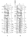
図1〜図4の各AおよびBは、マイクロマシン混載の電子回路装置の製造方法の一例の各製造工程の概略断面図である。
この例では、共通の基板上に、高周波共振器を構成するマイクロマシン素子(すなわち微小電気機械素子)とその周辺回路による電子回路が形成された高周波フィルタを構成するマイクロマシン混載の電子回路装置を例示したものである。
この場合、図1Aに示すように、例えばシリコン半導体より成る基板1に、電子回路を構成する回路素子2を形成する。この回路素子2は、通常の半導体集積回路の製造方法と同様の周知の方法によって形成される。図においては、回路素子として、CMOSを構成する1つのMOSのみが開示されている。
シリコン基板1の回路素子の形成部以外のフィールド部には、例えば局部的熱酸化(LOCOS:Local Oxidation of silicon)による素子分離絶縁層3が形成されている。
Embodiments of a micromachine mixed electronic circuit device and a method of manufacturing a micromachine and electronic circuit mixed device according to the present invention will be described with reference to the drawings. However, the present invention is not limited to this example. Needless to say.
1 to 4 are schematic cross-sectional views of manufacturing steps of an example of a method for manufacturing a micromachine mixed electronic circuit device.
In this example, a micromachine mixed electronic circuit device constituting a high frequency filter in which a micromachine element (that is, a microelectromechanical element) constituting a high frequency resonator and an electronic circuit of its peripheral circuit are formed on a common substrate is illustrated. Is.
In this case, as shown in FIG. 1A, a
In a field part other than the circuit element formation part of the
シリコン基板1上には、例えばCVD(Chemical Vapor Deposition)によってSiO2による下層絶縁層9dが被着形成される。
そして、下層絶縁層9d上のマイクロマシン素子すなわち共振器の形成部に、エッチングストップ層4と、その上に共振器の導電パターン5を形成する。
エッチングストップ層4は、例えば減圧CVDによってSiN層を全面的に形成し、フォトリソグラフィによって、不要部分をエッチング除去して形成する。
導電パターン5は、例えばりん(P)ドープのポリシリコンを、同様に全面的に形成し、フォトリソグラフィによって所要のパターンに形成する。この導電パター5は、MEMS共振器の機械的振動がなされるマイクロマシン動作構造部に対する電荷供給がなされる端子パター51および52と、入力信号線5iと出力信号線5oとが形成される。
On the
Then, the
The
As the
図1Bに示すように、導電パターン5上のMEMS素子の形成部に犠牲層6を形成する。この犠牲層6は例えばCVDによる酸化シリコン例えばSiO2層を全面的に形成し、同様にフォトリソグラフィによってパターン化し、端子パターン51および52上の、最終的に形成されるマイクロマシン動作構造部7の支持部、すなわち橋脚を構成する部分に開口6aが形成されたパターンとする。
As shown in FIG. 1B, a
次に、図2Aに示すように、犠牲層6上に、その開口6a内を含めて例えばCVDによってポリシリコン層を形成し、これをフォトリソグラフィによってパターン化し、例えば平面形状が直方形状のマイクロマシン動作構造部7を形成する。
その後、導電パターン5およびマイクロマシン動作構造部7の活性化処理を通常の不純物活性化条件で行う。この処理は、例えば窒素雰囲気中で800℃〜900℃の熱処理によって行なう。
そして図2Bに示すように、配線部8を形成する。この配線部8は、通常におけるように、例えば多層の配線層間絶縁層9の介在によって多層の配線パターン10が積層される。積層された所定の配線パターン10間が、配線層間絶縁層9に貫通して形成された貫通孔いわゆるビアホール内に形成された連結導電体10cを介して接続されて構成される。この場合、通常の半導体集積回路装置におけると同様に、その配線層間絶縁層9は、電子回路の形成部およびマイクロマシンの形成部上を含んで全面的に堆積させる。この配線層間絶縁層9は、犠牲層6とエッチング液が共通のSiO2によって構成される。
Next, as shown in FIG. 2A, a polysilicon layer is formed on the
Thereafter, the activation process of the
Then, as shown in FIG. 2B, the
次に、図3Aに示すように、少なくともマイクロマシン動作構造部7の形成部と配線部8との間に介在されるように、例えばマイクロマシン動作構造部7を取り囲んで、かつマイクロマシン動作構造部7の周辺から所要の間隙を隔てた位置に、溝11を配線層間絶縁層9を横切る深さに、例えばドライエッチングによる異方性エッチングによって形成する。
Next, as shown in FIG. 3A, for example, the micromachine
図3Bに示すように、エッチングに耐性を有し、低温で溝11内を良好に埋め込むことができる保護材料層12M、例えばSiNエッチング保護材を例えばプラズマCVDによって形成して溝11内を充填する。このよういして溝11内にエッチング保護壁12を形成する。
As shown in FIG. 3B, a
図4Aに示すように、エッチング保護材料層12Mの、マイクロマシン動作構造部7の配置部上にエッチング用開口12aを、フォトリソグラフィ技術の適用によって形成する。
次に、図4Bに示すように、この開口12aを通じて、フッ酸によるウエットエッチング、すなわち等方性エッチングによって配線層間絶縁層9と犠牲層6とをエッチング除去して、空洞部13を形成する。
また、配線部8の外部に接続する配線パターン10上の配線層間絶縁層9にコンタクト窓18をフォトリソグラフィによるパターンエッチングによって開口する。
As shown in FIG. 4A, an etching opening 12a is formed on the arrangement portion of the micromachine
Next, as shown in FIG. 4B, through the opening 12a, the wiring
Further, a
このようにして、空洞部13内に、犠牲層6の排除によってマイクロマシン動作構造部7が、犠牲層6の開口6aを通じて端子パターン51および52に連結された橋脚による支持部14以外のすべてがその全周辺すなわち全外表面が他部と離間した構成とされ、その機械的動作、この例では、振動が阻害されることがない中空構造によるマイクロマシン動作構造部7を有するマイクロマシン素子15が構成される。そして、このマイクロマシン素子15が形成された共通の基板1に、回路素子2と配線部8を有する電子回路16が形成された目的とするマイクロマシン混載の電子回路装置17が構成される。
In this way, in the cavity 13, the micromachine
この構成によるマイクロマシン混載の電子回路装置17は、端子リード51および52によって、マイクロマシン動作構造部7に所要の電圧を印加することによってこのマイクロマシン動作構造部7に静電荷が蓄積された状態で、入力信号線5iに入力信号を導入すると、マイクロマシン動作構造部7の固有振動数に一致する周波数の入力信号によってマイクロマシン動作構造部7が共鳴し、大きい振幅を持って振動する。これによってマイクロマシン素子15と周辺回路を構成する電子回路部16とによって所定の周波数のフィルタ回路を構成することができる。
The electronic circuit device 17 mixed with a micromachine having this configuration is applied to the micromachine
そして、この構成によるマイクロマシン混載の電子回路装置17は、マイクロマシン動作構造部7とこれに隣接する電子回路部16との間にエッチング保護壁12が介在された構成によることから、電子回路部16の特に配線パターンの配線層間絶縁層10が、空洞部13を形成するエッチングによって損傷することによる絶縁性の低下、これによる配線パターンの電気的、機械的特性の経時劣化を回避することができる。
The electronic circuit device 17 mixed with a micromachine having this configuration is based on a configuration in which an
また、本発明製造方法によれば、配線層間絶縁層10に対するマイクロマシン動作構造部7の可動化の空洞部13の形成をマイクロマシン動作構造部7から離間した位置にエッチング保護壁を設けて行なうようにしたことから、電子回路部16の配線部への影響を回避でき、マイクロマシン動作構造部7下の犠牲層6の排除のエッチングを含めて確実に行うことができる。
したがって、電子回路の信頼性を損なうことなく、マイクロマシンの動作が確実になされる空洞部の形成を行うことができるものである。
Further, according to the manufacturing method of the present invention, the cavity 13 for movability of the micromachine
Therefore, it is possible to form a cavity where the operation of the micromachine can be performed reliably without impairing the reliability of the electronic circuit.
上述した製造方法においては、空洞部13をウエットエッチングのみによって形成した場合であるが、ウエットエッチングに先立ってドライエッチングによって所要の深さまでのエッチングを行い、その後、上述したウエットエッチングによって行なうことができる。
図1〜図4で示した例では、最終的にエッチング保護壁を残存させた構成とした場合であるが、最終的にエッチング保護壁が残存されない構成の電子回路装置を構成することもできる。
In the manufacturing method described above, the cavity 13 is formed only by wet etching. However, etching can be performed to a required depth by dry etching prior to wet etching, and then performed by the above-described wet etching. .
The example shown in FIGS. 1 to 4 is a case where the etching protection wall is finally left, but an electronic circuit device having a structure in which the etching protection wall does not remain can be configured.
図5〜図7の各AおよびBは、それぞれ本発明製造方法の他の例の各工程の要部の断面図である。
これら図5〜図7図を参照して本発明製造方法の他の例を説明する。
Each of A and B in FIGS. 5 to 7 is a cross-sectional view of the main part of each step of another example of the production method of the present invention.
Another example of the manufacturing method of the present invention will be described with reference to FIGS.
この例においても図5Aに示すように、例えば前述した図1および図2で説明したと同様の方法によって、共通のシリコン半導体による基板1に、回路素子2、配線層間絶縁層9と配線パターン10が形成された配線部8、マイクロマシン動作構造部7等の形成を行う。
Also in this example, as shown in FIG. 5A, the
そして、この例においては、堆積された配線層間絶縁層9上に、全面的に例えばプラズマCVDによってSiNによるパッシベーション膜19を形成する。
次に、この例においては、図5Bに示すように、配線部8の外部に接続する配線パターン10上の配線層間絶縁層9とパッシベーション膜19に渡ってコンタクト窓18と、最終的にマイクロマシンを構成する空洞部13の形成部上に、凹部20を形成する。
In this example, a
Next, in this example, as shown in FIG. 5B, the
次に、図6Aに示すように、図3Aで説明したと同様に、少なくともマイクロマシン動作構造部7の形成部と配線部8との間に介在されるように、例えばマイクロマシン動作構造部7を取り囲んで、かつマイクロマシン動作構造部7の周辺から所要の間隙を隔てた位置に、溝11を配線層間絶縁層9を横切る深さに、例えばドライエッチングによる異方性エッチングによって形成する。
図6Bに示すように、例えばフォトレジストをスピンコートし溝11内に、低温で、溝11内を良好に埋め込むことができるフォトレジストを充填して、エチング保護壁12を形成すると共に、コンタクト窓18を覆う保護膜23を形成する。この保護膜23の凹部20上には、開口22を形成する。
Next, as shown in FIG. 6A, as described in FIG. 3A, for example, the micromachine
As shown in FIG. 6B, for example, a photoresist is spin-coated, and the
図7Aに示すように、開口22を通じてフォトレジストによる保護壁12が耐性を有するBHF(バッファドフッ酸)のエッチングによるウエットエッチングによる等方性エッチングを行なって配線層間絶縁層9および犠牲層6のエッチング除去をおこなって空洞部13を形成する。
その後、図7Bに示すように、エッチング保護壁12と保護膜23をその溶剤によって除去する。
As shown in FIG. 7A, isotropic etching is performed by wet etching by etching of BHF (buffered hydrofluoric acid) with which the
Thereafter, as shown in FIG. 7B, the etching
このようにして、空洞部13内に、犠牲層6の排除によってマイクロマシン動作構造部7が、犠牲層6の開口6aを通じて端子パターン51および52に連結された橋脚による支持部14以外のすべてがその全周辺すなわち全外表面が他部と離間した構成とされ、その機械的動作、この例では、振動が阻害されることがないマイクロマシン動作構造部7を有するマイクロマシン素子15が構成される。そして、このマイクロマシン素子15が形成された共通の基板1に、回路素子2と配線部8を有する電子回路16が形成された目的とするマイクロマシン混載の電子回路装置17が構成される。
In this way, in the cavity 13, the micromachine
この製造方法による場合においても、前述した例と同様に、空洞部13の形成を容易に、かつ他部への影響を効果的に回避することができる。
したがって、本発明によれば、信頼性の高いマイクロマシン混載の電気回路装置を構成することができる。
Also in the case of this manufacturing method, as in the above-described example, the formation of the cavity 13 can be easily performed and the influence on other parts can be effectively avoided.
Therefore, according to the present invention, a highly reliable electric circuit device mixed with a micromachine can be configured.
この例では、マイクロマシン混載の電子回路装置17として、エッチング保護壁12が排除された構成としたが、エッチング保護壁12の材料選定を行うことによってエッチング保護壁12が残存させる構成とすることもできる。
なお、図5〜図7において、図1〜図4図に対応する部分には同一符号を付して重複説明を省略する。
In this example, as the electronic circuit device 17 mixed with a micromachine, the
5-7, the same code | symbol is attached | subjected to the part corresponding to FIGS. 1-4, and duplication description is abbreviate | omitted.
上述した各構成および製造方法において、空洞部13を構成するウエットエッチングは、マイクロマシン15の構成材の例えばポリシリコンを侵食しないか極めて侵食性が低く、また、配線層間絶縁層9および犠牲層6の構成材例えばSiO2に対して高いエッチング性を有し、エッチングストップ層およびエッチング保護壁12の構成材の例えばSiNに対してエッチング性がないか十分低いエッチング液の例えばフッ酸系のエッチング液を用いることができる。そして、エッチング保護壁12の構成材としてフォトレジストが用いられる場合は、空洞部13を形成するエッチング液は、BHF(バッファドフッ酸)を用いることができる。
In each of the above-described configurations and manufacturing methods, the wet etching that forms the cavity 13 does not erode, for example, polysilicon of the constituent material of the micromachine 15 or has extremely low erodibility, and the wiring
上述した例では、エッチング保護壁12を構成するエッチング保護材料が、犠牲層6が、酸化シリコンである場合において、フォトレジスト層、あるいはプラズマCVDによるSiNとしたが、エッチング保護材料は、これに限定されるものではない。犠牲層6のエッチャントに対する耐性を有し、かつメタルハイブリッド戦争にダメージを与えない程度(一般に400℃以下)の温度で溝11内を良好に充填することができる材料であればよく、例えば有機系ではポリイミド、無機系ではプラズマCVDによるアモルファスシリコンなどによっても構成することができる。
In the above-described example, the etching protective material constituting the etching
また、上述した例では、基板1がシリコン基板である場合を例示したが、絶縁ないしは半絶縁基体上に半導体層が形成された基板を用いることもできるなど、本発明は、上述した例に限られるものではなく、種々の変形、変更を行うことができるものである。
In the above example, the
1……基板、2……回路素子、3……素子分離絶縁層、4……エッチングストップ層、5……導電パターン,5i……入力信号線、5o……出力信号線、6……犠牲層、6a……開口、7……マイクロマシン動作構造部、8……配線部、9……配線層間絶縁層、9d……下層絶縁層、10……配線パターン、10c……連結導電体、11……溝、12a……エッチング用開口、12……エッチング保護壁、12M……エッチング保護材料層、13……空洞部、17……マイクロマシン混載の電子回路装置、18……コンタクト窓、19……パッシベーション膜、20……凹部、22……開口、23……保護膜、51,52……端子パターン
DESCRIPTION OF
Claims (2)
上記基板上の電子回路の形成部に形成された電子回路素子と、
上記電子回路の形成部上に形成され、配線層間絶縁層を介して多層の配線パターンが積層された配線部と、
上記基板のマイクロマシン素子の形成部上に対応して、上記配線層間絶縁膜と連続する配線層間絶縁層に形成された空洞部と、
上記配線層間絶縁層の上記空洞部の内側壁面に配置されたエッチング保護壁と、
上記空洞部内の上記基板上に形成され、上記配線部の最上層の配線パターンより下方位置に存する導電パターン及びマイクロマシン動作構造部からなるマイクロマシン素子と、
上記マイクロマシン素子の導電パターンの下に配置されたエッチングストップ層と
を有し、
上記マイクロマシン素子は、上記空洞部内に上記マイクロマシン動作構造部の機械的支持部以外の全外表面が他部と非接触状態で露出して、保持されている
ことを特徴とするマイクロマシン混載の電子回路装置。 A micromachine mixed electronic circuit device in which a micromachine element and an electronic circuit are mixedly mounted on a common substrate,
An electronic circuit element formed in the electronic circuit forming part on the substrate;
A wiring part formed on the electronic circuit forming part and having a multilayer wiring pattern laminated via a wiring interlayer insulating layer;
Corresponding to the formation part of the micromachine element of the substrate, a cavity part formed in the wiring interlayer insulating layer continuous with the wiring interlayer insulating film,
An etching protective wall disposed on the inner wall surface of the cavity of the wiring interlayer insulating layer;
A micromachine element comprising a conductive pattern and a micromachine operation structure portion formed on the substrate in the cavity portion and located at a lower position than the uppermost wiring pattern of the wiring portion;
An etching stop layer disposed under the conductive pattern of the micromachine element,
The micromachine element is an electronic circuit mixed with a micromachine, characterized in that the entire outer surface other than the mechanical support portion of the micromachine operation structure portion is exposed and held in a non-contact state with the other portion in the cavity portion. apparatus.
上記基板上の電子回路の形成部に、電子回路素子を形成する第1工程と、
上記基板上のマイクロマシン素子の形成部に、エッチングストップ層を形成し、該エッチングストップ層上にマイクロマシン素子の導電パターンを形成する第2工程と、
上記導電パターン上の上記マイクロマシン素子の形成部に犠牲層を形成する第3工程と、
上記犠牲層上に、上記マイクロマシン素子の機械的動作がなされるマイクロマシン動作構造部を形成する第4工程と、
上記導電パターン及び上記マイクロマシン動作構造部の活性化のための熱処理を行う第5工程と、
上記電子回路の形成部上に、配線層間絶縁層を介して多層の配線パターンが積層された配線部を形成し、上記マイクロマシン素子の形成部上に、上記マイクロマシン動作構造部が埋め込まれるように上記配線層間絶縁層のみを形成する第6工程と、
少なくとも上記マイクロマシン動作構造物と少なくとも上記電子回路部との間に上記マイクロマシン動作構造部と所定の距離を隔てて、上記配線層間絶縁層に溝を掘り込む第7工程と、
上記溝内に耐エッチング材を充填してエッチング保護壁を形成する第8工程と、
上記配線層間絶縁層に、上記マイクロマシン動作構造部を露出する開口を形成すると共に、上記マイクロマシン動作構造部の下の上記犠牲層をエッチング除去する第9工程とを有し、
上記マイクロマシン動作構造部の配置部に、該マイクロマシン動作構造部の機械的支持部以外の全外表面が、他部と非接触状態を保持する空洞部が形成されるようにした
ことを特徴とするマイクロマシン混載の電子回路装置の製造方法。 A method of manufacturing a micromachine mixed electronic circuit device in which a micromachine element and an electronic circuit are mixedly mounted on a common substrate,
A first step of forming an electronic circuit element on the electronic circuit forming portion on the substrate;
A second step of forming an etching stop layer on a formation portion of the micromachine element on the substrate and forming a conductive pattern of the micromachine element on the etching stop layer;
A third step of forming a sacrificial layer in the formation portion of the micromachine element on the conductive pattern;
A fourth step of forming on the sacrificial layer a micromachine operation structure portion in which the mechanical operation of the micromachine element is performed;
A fifth step of performing a heat treatment for activating the conductive pattern and the micromachine operating structure;
A wiring part in which a multilayer wiring pattern is laminated via a wiring interlayer insulating layer is formed on the electronic circuit forming part, and the micromachine operation structure part is embedded on the micromachine element forming part. A sixth step of forming only the wiring interlayer insulating layer;
A seventh step of digging a groove in the wiring interlayer insulating layer at a predetermined distance from the micromachine operation structure portion between at least the micromachine operation structure and at least the electronic circuit portion;
An eighth step of forming an etching protective wall by filling the groove with an etching resistant material;
Forming an opening in the wiring interlayer insulating layer to expose the micromachine operation structure, and etching and removing the sacrificial layer under the micromachine operation structure.
The placement portion of the micromachine operation structure portion is formed with a cavity portion in which the entire outer surface other than the mechanical support portion of the micromachine operation structure portion maintains a non-contact state with the other portions. A method of manufacturing an electronic circuit device mixed with a micromachine.
Priority Applications (1)
| Application Number | Priority Date | Filing Date | Title |
|---|---|---|---|
| JP2005325009A JP4857718B2 (en) | 2005-11-09 | 2005-11-09 | Micromachine mixed electronic circuit device and method for manufacturing micromachine mixed electronic circuit device |
Applications Claiming Priority (1)
| Application Number | Priority Date | Filing Date | Title |
|---|---|---|---|
| JP2005325009A JP4857718B2 (en) | 2005-11-09 | 2005-11-09 | Micromachine mixed electronic circuit device and method for manufacturing micromachine mixed electronic circuit device |
Publications (2)
| Publication Number | Publication Date |
|---|---|
| JP2007134453A JP2007134453A (en) | 2007-05-31 |
| JP4857718B2 true JP4857718B2 (en) | 2012-01-18 |
Family
ID=38155881
Family Applications (1)
| Application Number | Title | Priority Date | Filing Date |
|---|---|---|---|
| JP2005325009A Expired - Fee Related JP4857718B2 (en) | 2005-11-09 | 2005-11-09 | Micromachine mixed electronic circuit device and method for manufacturing micromachine mixed electronic circuit device |
Country Status (1)
| Country | Link |
|---|---|
| JP (1) | JP4857718B2 (en) |
Families Citing this family (3)
| Publication number | Priority date | Publication date | Assignee | Title |
|---|---|---|---|---|
| JP2011049303A (en) | 2009-08-26 | 2011-03-10 | Toshiba Corp | Electric component and method of manufacturing the same |
| DE102015206996A1 (en) * | 2015-04-17 | 2016-10-20 | Robert Bosch Gmbh | Method for producing microelectromechanical structures in a layer sequence and a corresponding electronic component having a microelectromechanical structure |
| DE102017218883A1 (en) * | 2017-10-23 | 2019-04-25 | Fraunhofer-Gesellschaft zur Förderung der angewandten Forschung e.V. | Microelectromechanical component and a method for its production |
Family Cites Families (5)
| Publication number | Priority date | Publication date | Assignee | Title |
|---|---|---|---|---|
| EP0822579B1 (en) * | 1996-07-31 | 2004-07-21 | STMicroelectronics S.r.l. | Intergrated microstructures and a method of fabricating thereof |
| JP4081868B2 (en) * | 1998-08-10 | 2008-04-30 | 日産自動車株式会社 | Manufacturing method of micro device |
| EP1028466B1 (en) * | 1999-02-09 | 2006-08-02 | STMicroelectronics S.r.l. | Method for manufacturing integrated devices including electromechanical microstructures, without residual stress |
| JP2002246363A (en) * | 2001-02-21 | 2002-08-30 | Sony Corp | Method for manufacturing semiconductor device |
| JP4772302B2 (en) * | 2003-09-29 | 2011-09-14 | パナソニック株式会社 | Micro-electromechanical system and manufacturing method thereof |
-
2005
- 2005-11-09 JP JP2005325009A patent/JP4857718B2/en not_active Expired - Fee Related
Also Published As
| Publication number | Publication date |
|---|---|
| JP2007134453A (en) | 2007-05-31 |
Similar Documents
| Publication | Publication Date | Title |
|---|---|---|
| US8551798B2 (en) | Microstructure with an enhanced anchor | |
| JP5602761B2 (en) | Micro-electromechanical system device having separated microstructure and manufacturing method thereof | |
| JP4799059B2 (en) | Semiconductor device | |
| US7932118B2 (en) | Method of producing mechanical components of MEMS or NEMS structures made of monocrystalline silicon | |
| JP2006289520A (en) | Semiconductor device using mems technology | |
| JP2006326806A (en) | Semiconductor device using mems technique | |
| JP2009150863A (en) | Sensor having driver electrode independent of location in multilayer silicon-on-insulator substrate | |
| US20140151823A1 (en) | Mems devices and methods of forming same | |
| US8704317B2 (en) | Microstructure device with an improved anchor | |
| US20120104593A1 (en) | Electronic device and method for manufacturing electronic device | |
| JP4544140B2 (en) | MEMS element | |
| US6794271B2 (en) | Method for fabricating a microelectromechanical system (MEMS) device using a pre-patterned bridge | |
| US6761829B2 (en) | Method for fabricating an isolated microelectromechanical system (MEMS) device using an internal void | |
| CN104627948A (en) | Micromechanical sensor device and corresponding manufacturing method | |
| JP4857718B2 (en) | Micromachine mixed electronic circuit device and method for manufacturing micromachine mixed electronic circuit device | |
| JP2008137139A (en) | Micro electro-mechanical system and its manufacturing method | |
| JP4501715B2 (en) | MEMS element and method for manufacturing MEMS element | |
| US7531424B1 (en) | Vacuum wafer-level packaging for SOI-MEMS devices | |
| JP4333417B2 (en) | Micromachine manufacturing method | |
| JP2006224219A (en) | Manufacturing method for mems element | |
| JP5145412B2 (en) | Micromechanical element and method for manufacturing micromechanical element with thin film cap | |
| JP2009078315A (en) | Sealing structure and its manufacturing method | |
| JP4774902B2 (en) | Manufacturing method of MEMS element | |
| TWI506694B (en) | Semiconductor device and method for forming a semiconductor device | |
| JP2010207987A (en) | Method of manufacturing micromachine device |
Legal Events
| Date | Code | Title | Description |
|---|---|---|---|
| A621 | Written request for application examination |
Free format text: JAPANESE INTERMEDIATE CODE: A621 Effective date: 20080910 |
|
| A977 | Report on retrieval |
Free format text: JAPANESE INTERMEDIATE CODE: A971007 Effective date: 20101130 |
|
| A131 | Notification of reasons for refusal |
Free format text: JAPANESE INTERMEDIATE CODE: A131 Effective date: 20101207 |
|
| A521 | Written amendment |
Free format text: JAPANESE INTERMEDIATE CODE: A523 Effective date: 20110126 |
|
| A131 | Notification of reasons for refusal |
Free format text: JAPANESE INTERMEDIATE CODE: A131 Effective date: 20110705 |
|
| A521 | Written amendment |
Free format text: JAPANESE INTERMEDIATE CODE: A523 Effective date: 20110826 |
|
| TRDD | Decision of grant or rejection written | ||
| A01 | Written decision to grant a patent or to grant a registration (utility model) |
Free format text: JAPANESE INTERMEDIATE CODE: A01 Effective date: 20111004 |
|
| A01 | Written decision to grant a patent or to grant a registration (utility model) |
Free format text: JAPANESE INTERMEDIATE CODE: A01 |
|
| A61 | First payment of annual fees (during grant procedure) |
Free format text: JAPANESE INTERMEDIATE CODE: A61 Effective date: 20111017 |
|
| FPAY | Renewal fee payment (event date is renewal date of database) |
Free format text: PAYMENT UNTIL: 20141111 Year of fee payment: 3 |
|
| LAPS | Cancellation because of no payment of annual fees |