JP4856758B2 - Devices using integrated and integrated photonics modules - Google Patents
Devices using integrated and integrated photonics modules Download PDFInfo
- Publication number
- JP4856758B2 JP4856758B2 JP2009505501A JP2009505501A JP4856758B2 JP 4856758 B2 JP4856758 B2 JP 4856758B2 JP 2009505501 A JP2009505501 A JP 2009505501A JP 2009505501 A JP2009505501 A JP 2009505501A JP 4856758 B2 JP4856758 B2 JP 4856758B2
- Authority
- JP
- Japan
- Prior art keywords
- modulated
- scanner
- light
- photonics module
- integrated photonics
- Prior art date
- Legal status (The legal status is an assumption and is not a legal conclusion. Google has not performed a legal analysis and makes no representation as to the accuracy of the status listed.)
- Active
Links
- 230000010287 polarization Effects 0.000 claims description 39
- 239000002131 composite material Substances 0.000 claims description 13
- 230000000737 periodic effect Effects 0.000 claims description 8
- 230000010354 integration Effects 0.000 claims description 4
- 230000003287 optical effect Effects 0.000 description 70
- 238000010586 diagram Methods 0.000 description 27
- 238000007493 shaping process Methods 0.000 description 24
- 238000000034 method Methods 0.000 description 22
- 230000005540 biological transmission Effects 0.000 description 15
- 230000033001 locomotion Effects 0.000 description 10
- 230000006870 function Effects 0.000 description 8
- 238000012937 correction Methods 0.000 description 6
- 239000013307 optical fiber Substances 0.000 description 6
- 230000008569 process Effects 0.000 description 6
- 230000003044 adaptive effect Effects 0.000 description 5
- 238000000576 coating method Methods 0.000 description 5
- 238000001514 detection method Methods 0.000 description 5
- 238000009826 distribution Methods 0.000 description 5
- 210000001747 pupil Anatomy 0.000 description 5
- 239000011248 coating agent Substances 0.000 description 4
- 238000013461 design Methods 0.000 description 4
- 230000000694 effects Effects 0.000 description 4
- 229910052751 metal Inorganic materials 0.000 description 4
- 239000002184 metal Substances 0.000 description 4
- 230000010355 oscillation Effects 0.000 description 4
- 125000006850 spacer group Chemical group 0.000 description 4
- 230000001154 acute effect Effects 0.000 description 3
- 239000000853 adhesive Substances 0.000 description 3
- 230000001070 adhesive effect Effects 0.000 description 3
- 238000004458 analytical method Methods 0.000 description 3
- 238000013459 approach Methods 0.000 description 3
- 201000009310 astigmatism Diseases 0.000 description 3
- 230000008878 coupling Effects 0.000 description 3
- 238000010168 coupling process Methods 0.000 description 3
- 238000005859 coupling reaction Methods 0.000 description 3
- 238000000708 deep reactive-ion etching Methods 0.000 description 2
- 239000000835 fiber Substances 0.000 description 2
- 239000011521 glass Substances 0.000 description 2
- 238000003384 imaging method Methods 0.000 description 2
- 238000003754 machining Methods 0.000 description 2
- 238000004519 manufacturing process Methods 0.000 description 2
- 238000012544 monitoring process Methods 0.000 description 2
- 230000010363 phase shift Effects 0.000 description 2
- 210000001525 retina Anatomy 0.000 description 2
- 238000005070 sampling Methods 0.000 description 2
- 239000007787 solid Substances 0.000 description 2
- 230000001360 synchronised effect Effects 0.000 description 2
- RZVAJINKPMORJF-UHFFFAOYSA-N Acetaminophen Chemical compound CC(=O)NC1=CC=C(O)C=C1 RZVAJINKPMORJF-UHFFFAOYSA-N 0.000 description 1
- KWYUFKZDYYNOTN-UHFFFAOYSA-M Potassium hydroxide Chemical compound [OH-].[K+] KWYUFKZDYYNOTN-UHFFFAOYSA-M 0.000 description 1
- XUIMIQQOPSSXEZ-UHFFFAOYSA-N Silicon Chemical compound [Si] XUIMIQQOPSSXEZ-UHFFFAOYSA-N 0.000 description 1
- RTAQQCXQSZGOHL-UHFFFAOYSA-N Titanium Chemical compound [Ti] RTAQQCXQSZGOHL-UHFFFAOYSA-N 0.000 description 1
- 206010047571 Visual impairment Diseases 0.000 description 1
- 230000004913 activation Effects 0.000 description 1
- 230000006978 adaptation Effects 0.000 description 1
- 229910052782 aluminium Inorganic materials 0.000 description 1
- XAGFODPZIPBFFR-UHFFFAOYSA-N aluminium Chemical compound [Al] XAGFODPZIPBFFR-UHFFFAOYSA-N 0.000 description 1
- 230000003139 buffering effect Effects 0.000 description 1
- 238000006243 chemical reaction Methods 0.000 description 1
- 150000001875 compounds Chemical class 0.000 description 1
- 230000001419 dependent effect Effects 0.000 description 1
- 238000004512 die casting Methods 0.000 description 1
- 239000003989 dielectric material Substances 0.000 description 1
- 235000019800 disodium phosphate Nutrition 0.000 description 1
- 238000004146 energy storage Methods 0.000 description 1
- 238000005516 engineering process Methods 0.000 description 1
- 238000005530 etching Methods 0.000 description 1
- 230000005284 excitation Effects 0.000 description 1
- 239000011213 glass-filled polymer Substances 0.000 description 1
- 238000005286 illumination Methods 0.000 description 1
- 238000002347 injection Methods 0.000 description 1
- 239000007924 injection Substances 0.000 description 1
- 238000009434 installation Methods 0.000 description 1
- 239000012212 insulator Substances 0.000 description 1
- 239000000463 material Substances 0.000 description 1
- 238000005259 measurement Methods 0.000 description 1
- 239000002991 molded plastic Substances 0.000 description 1
- 229910021421 monocrystalline silicon Inorganic materials 0.000 description 1
- 238000004091 panning Methods 0.000 description 1
- 239000004033 plastic Substances 0.000 description 1
- 229920000642 polymer Polymers 0.000 description 1
- 238000012545 processing Methods 0.000 description 1
- 230000000750 progressive effect Effects 0.000 description 1
- 239000005297 pyrex Substances 0.000 description 1
- 230000009467 reduction Effects 0.000 description 1
- 230000002207 retinal effect Effects 0.000 description 1
- 238000007789 sealing Methods 0.000 description 1
- 229910052710 silicon Inorganic materials 0.000 description 1
- 239000010703 silicon Substances 0.000 description 1
- 230000003068 static effect Effects 0.000 description 1
- 238000003860 storage Methods 0.000 description 1
- 230000003746 surface roughness Effects 0.000 description 1
- 238000010408 sweeping Methods 0.000 description 1
- 239000010936 titanium Substances 0.000 description 1
- 229910052719 titanium Inorganic materials 0.000 description 1
- 239000012780 transparent material Substances 0.000 description 1
Images


Classifications
-
- G—PHYSICS
- G09—EDUCATION; CRYPTOGRAPHY; DISPLAY; ADVERTISING; SEALS
- G09G—ARRANGEMENTS OR CIRCUITS FOR CONTROL OF INDICATING DEVICES USING STATIC MEANS TO PRESENT VARIABLE INFORMATION
- G09G3/00—Control arrangements or circuits, of interest only in connection with visual indicators other than cathode-ray tubes
- G09G3/02—Control arrangements or circuits, of interest only in connection with visual indicators other than cathode-ray tubes by tracing or scanning a light beam on a screen
- G09G3/025—Control arrangements or circuits, of interest only in connection with visual indicators other than cathode-ray tubes by tracing or scanning a light beam on a screen with scanning or deflecting the beams in two directions or dimensions
-
- G—PHYSICS
- G02—OPTICS
- G02B—OPTICAL ELEMENTS, SYSTEMS OR APPARATUS
- G02B27/00—Optical systems or apparatus not provided for by any of the groups G02B1/00 - G02B26/00, G02B30/00
- G02B27/10—Beam splitting or combining systems
- G02B27/1006—Beam splitting or combining systems for splitting or combining different wavelengths
- G02B27/102—Beam splitting or combining systems for splitting or combining different wavelengths for generating a colour image from monochromatic image signal sources
- G02B27/104—Beam splitting or combining systems for splitting or combining different wavelengths for generating a colour image from monochromatic image signal sources for use with scanning systems
-
- G—PHYSICS
- G02—OPTICS
- G02B—OPTICAL ELEMENTS, SYSTEMS OR APPARATUS
- G02B27/00—Optical systems or apparatus not provided for by any of the groups G02B1/00 - G02B26/00, G02B30/00
- G02B27/10—Beam splitting or combining systems
- G02B27/1066—Beam splitting or combining systems for enhancing image performance, like resolution, pixel numbers, dual magnifications or dynamic range, by tiling, slicing or overlapping fields of view
-
- G—PHYSICS
- G02—OPTICS
- G02B—OPTICAL ELEMENTS, SYSTEMS OR APPARATUS
- G02B27/00—Optical systems or apparatus not provided for by any of the groups G02B1/00 - G02B26/00, G02B30/00
- G02B27/10—Beam splitting or combining systems
- G02B27/14—Beam splitting or combining systems operating by reflection only
- G02B27/145—Beam splitting or combining systems operating by reflection only having sequential partially reflecting surfaces
-
- H—ELECTRICITY
- H04—ELECTRIC COMMUNICATION TECHNIQUE
- H04N—PICTORIAL COMMUNICATION, e.g. TELEVISION
- H04N9/00—Details of colour television systems
- H04N9/12—Picture reproducers
- H04N9/31—Projection devices for colour picture display, e.g. using electronic spatial light modulators [ESLM]
- H04N9/3102—Projection devices for colour picture display, e.g. using electronic spatial light modulators [ESLM] using two-dimensional electronic spatial light modulators
- H04N9/3111—Projection devices for colour picture display, e.g. using electronic spatial light modulators [ESLM] using two-dimensional electronic spatial light modulators for displaying the colours sequentially, e.g. by using sequentially activated light sources
-
- H—ELECTRICITY
- H04—ELECTRIC COMMUNICATION TECHNIQUE
- H04N—PICTORIAL COMMUNICATION, e.g. TELEVISION
- H04N9/00—Details of colour television systems
- H04N9/12—Picture reproducers
- H04N9/31—Projection devices for colour picture display, e.g. using electronic spatial light modulators [ESLM]
- H04N9/3129—Projection devices for colour picture display, e.g. using electronic spatial light modulators [ESLM] scanning a light beam on the display screen
-
- G—PHYSICS
- G02—OPTICS
- G02B—OPTICAL ELEMENTS, SYSTEMS OR APPARATUS
- G02B27/00—Optical systems or apparatus not provided for by any of the groups G02B1/00 - G02B26/00, G02B30/00
- G02B27/10—Beam splitting or combining systems
- G02B27/14—Beam splitting or combining systems operating by reflection only
- G02B27/141—Beam splitting or combining systems operating by reflection only using dichroic mirrors
-
- G—PHYSICS
- G02—OPTICS
- G02B—OPTICAL ELEMENTS, SYSTEMS OR APPARATUS
- G02B27/00—Optical systems or apparatus not provided for by any of the groups G02B1/00 - G02B26/00, G02B30/00
- G02B27/28—Optical systems or apparatus not provided for by any of the groups G02B1/00 - G02B26/00, G02B30/00 for polarising
- G02B27/283—Optical systems or apparatus not provided for by any of the groups G02B1/00 - G02B26/00, G02B30/00 for polarising used for beam splitting or combining
-
- G—PHYSICS
- G09—EDUCATION; CRYPTOGRAPHY; DISPLAY; ADVERTISING; SEALS
- G09G—ARRANGEMENTS OR CIRCUITS FOR CONTROL OF INDICATING DEVICES USING STATIC MEANS TO PRESENT VARIABLE INFORMATION
- G09G3/00—Control arrangements or circuits, of interest only in connection with visual indicators other than cathode-ray tubes
- G09G3/20—Control arrangements or circuits, of interest only in connection with visual indicators other than cathode-ray tubes for presentation of an assembly of a number of characters, e.g. a page, by composing the assembly by combination of individual elements arranged in a matrix no fixed position being assigned to or needed to be assigned to the individual characters or partial characters
- G09G3/34—Control arrangements or circuits, of interest only in connection with visual indicators other than cathode-ray tubes for presentation of an assembly of a number of characters, e.g. a page, by composing the assembly by combination of individual elements arranged in a matrix no fixed position being assigned to or needed to be assigned to the individual characters or partial characters by control of light from an independent source
- G09G3/3433—Control arrangements or circuits, of interest only in connection with visual indicators other than cathode-ray tubes for presentation of an assembly of a number of characters, e.g. a page, by composing the assembly by combination of individual elements arranged in a matrix no fixed position being assigned to or needed to be assigned to the individual characters or partial characters by control of light from an independent source using light modulating elements actuated by an electric field and being other than liquid crystal devices and electrochromic devices
- G09G3/346—Control arrangements or circuits, of interest only in connection with visual indicators other than cathode-ray tubes for presentation of an assembly of a number of characters, e.g. a page, by composing the assembly by combination of individual elements arranged in a matrix no fixed position being assigned to or needed to be assigned to the individual characters or partial characters by control of light from an independent source using light modulating elements actuated by an electric field and being other than liquid crystal devices and electrochromic devices based on modulation of the reflection angle, e.g. micromirrors
Landscapes
- Physics & Mathematics (AREA)
- Engineering & Computer Science (AREA)
- General Physics & Mathematics (AREA)
- Optics & Photonics (AREA)
- Multimedia (AREA)
- Signal Processing (AREA)
- Computer Hardware Design (AREA)
- Theoretical Computer Science (AREA)
- Mechanical Optical Scanning Systems (AREA)
- Investigating Or Analysing Materials By Optical Means (AREA)
Description
本発明は、統合型フォトニクスモジュールおよび統合型フォトニクスモジュールを用いたデバイスに関するものである。
2006年4月11日出願の米国特許仮出願第60/791,074号の優先権を主張し、本願明細書に参照によって組み込まれる。
The present invention relates to an integrated photonics module and a device using the integrated photonics module.
Claims priority of US Provisional Application No. 60 / 791,074 filed Apr. 11, 2006, which is incorporated herein by reference.
映像ディスプレイは、携帯型用途および固定位置用途をはじめとする種々の用途において用いられる。少なくとも一部分の用途において、および特に一部の携帯型用途において、視認可能なスクリーンサイズは、これまで製品パッケージの物理的な範囲によって制限されてきた。 Video displays are used in a variety of applications including portable and fixed location applications. In at least some applications, and particularly in some portable applications, the viewable screen size has so far been limited by the physical range of the product package.
統合型フォトニクスモジュールは、システムの範囲に統合されうるコンパクトな掃引ビームディスプレイを提供する。一部の実施形態によれば、コンパクトな掃引ビームディスプレイは、統合型フォトニクスモジュールを収容するシステム、製品またはパッケージの物理的範囲より大きい物理的範囲を有する画像を投影するように構成されてもよい。
本願出願は、2006年4月11日出願の米国特許仮出願第60/791,074号の優先権を主張し、本願明細書に参照によって組み込まれる。
The integrated photonics module provides a compact swept beam display that can be integrated into the range of the system. According to some embodiments, the compact swept beam display may be configured to project an image having a physical range that is greater than the physical range of the system, product or package that houses the integrated photonics module. .
This application claims priority from US Provisional Application No. 60 / 791,074, filed Apr. 11, 2006, and is incorporated herein by reference.
一部の実施形態によれば、統合型フォトニクスモジュールは、レーザなどの1つまたは複数の光源と、ビーム整形光学素子と、結合光学素子と、MEMSスキャナと、取り付けを容易にし、光学的配置を維持するための光学フレームなどの1つまたは複数の機械構成要素と、を含む。一部の実施形態によれば、統合型フォトニクスモジュールは、MEMS駆動電子機器、光源駆動電子機器、センサおよび映像電子機器の一部またはすべてを含みうる。種々の実施形態によれば、MEMS駆動電子機器としては、MEMSコントローラ、D/A変換器および/またはA/D変換器およびMEMS駆動増幅器などが挙げられうる。映像コントローラ電子機器としては、光源コントローラ、D/A変換器および光源駆動増幅器などが挙げられうる。他の実施形態によれば、統合型フォトニクスモジュールの出力は、光をリモートスキャナに供給するように構成されるファイバ結合器などのビームスキャナ用の異なるインターフェイスに置き換えてもよい。 According to some embodiments, the integrated photonics module facilitates installation and optical arrangement by one or more light sources such as lasers, beam shaping optics, coupling optics, MEMS scanners. One or more mechanical components, such as an optical frame to maintain. According to some embodiments, the integrated photonics module may include some or all of MEMS driven electronics, light source driven electronics, sensors, and video electronics. According to various embodiments, the MEMS drive electronics can include a MEMS controller, a D / A converter and / or an A / D converter and a MEMS drive amplifier, and the like. The video controller electronic device may include a light source controller, a D / A converter, a light source driving amplifier, and the like. According to other embodiments, the output of the integrated photonics module may be replaced with a different interface for a beam scanner such as a fiber coupler configured to provide light to a remote scanner.
図1は、実施形態による映像画像などの画像を表示するための統合型フォトニクスモジュール102を含む電子デバイス101のブロック図である。具体的な実施形態によれば、統合型フォトニクスモジュール102は、システムリソース104へのインターフェイスを含みうる。映像コントローラ電子機器106は、システムコントローラおよびソフトウェア108を含む統合型映像特定用途向け集積回路(ASIC)として具体化されてもよく、入力映像信号を受信する。映像コントローラ電子機器106は、映像メモリ110において受信した映像画像を少なくとも一時的にバッファに格納してもよく、映像メモリ110は、フレームバッファメモリおよびオンスクリーンディスプレイメニューを含んでもよい。新たな映像フレームを表示する時間である場合には、映像コントローラ電子機器106は、映像メモリ110からキャッシュに格納された映像フレームを読み出して、1つまたは複数の光源ドライバ112を順次駆動し、入力映像信号における画素値に対応する一連の輝度値にする。光源ドライバ112は、1つまたは複数の光源116を駆動し、光源116は、実施形態による統合型フォトニクスモジュール102の統合型光学エンジン部分114に含まれてもよい。光源116は、結合器およびビーム整形光学素子118によって整形されて、光119の変調合成ビームを結合しうる光の1つまたは複数の変調ビームを作成する。光源116は、たとえば、赤色変調レーザ、緑色変調レーザおよび青色変調レーザであってもよい。一部の実施形態によれば、光119の変調合成ビームは、スキャナ120に向かって指向されてもよく、スキャナ120は、たとえば、MEMSスキャナであってもよく、変調合成ビームを視野(FOV)にわたって走査可能にして、画像を形成する。
FIG. 1 is a block diagram of an
映像コントローラ電子機器106は、光源ドライバ112を駆動している間に、同時に、スキャナコントローラ122を駆動する。スキャナコントローラ122は、一部の実施形態によれば、スキャナコントローラおよびソフトウェア124も含んでもよいスキャナドライブASICとして任意に具体化されてもよい。スキャナコントローラ122は、スキャナ120を駆動してFOVにわたって発せられた光を順次走査して、周期的な走査パターンにおける光125の変調走査ビームとするように動作可能である。
The video controller
スキャナ120は、FOVにわたって光の変調ビームを偏向して、光125の走査ビームを生成する。光125の走査ビームは、任意に、最終光学素子126によって調整および/またはリレーされて、映像画像128を生成してもよい。
The
総合すれば、光源116、結合器およびビーム整形光学素子118およびスキャナ120は、機械的取り付け構造、アクチュエータなどと共に、統合型光学エンジン112を備えてもよく、統合型光学エンジン112は、今度は統合型フォトニクスモジュールを備えてもよい。光125の走査ビームの瞬時位置が、FOVにおけるスポットを順次照らす。FOVは、ディスプレイ表面、射出瞳拡大素子(EPE)または投影スクリーンを含む。画像を表示するために、FOVにおける実質的にすべてのスポットが、名目上、各スポットに対応する入力映像画像の画素の明度に比例するパワーの量で順次照らされる。
Taken together, the
ビームが、スポットを照らす間に、照らしている光ビームの一部が、反射または散乱エネルギとして散乱される。散乱された光エネルギの一部は、1つまたは複数の目視者130の方に進みうる。目視者の目および心における残像は、FOVにおいて照らされた一連のスポットを静止画像および/または動画像を含みうる認識可能な映像画像128に統合する。
While the beam illuminates the spot, a portion of the illuminating light beam is scattered as reflected or scattered energy. Some of the scattered light energy may travel toward one or
一部の実施形態によれば、光検出器(図示せず)はまた、FOVから散乱された光エネルギの一部を受信するように整列されてもよい。種々の処理は、受信された散乱光エネルギに施されて、機能性を提供してもよい。検出器の機能性の一部の実施形態は、統合型フォトニクスモジュールの一部として含まれてもよい。そのような検出器は、再帰集光または共焦点配置によって、スキャナからデスキャンされたエネルギを受信するように整列されてもよく、または凝視検出配置を介してFOVから直接的にまたはリレー光学素子を通って、光を受信するように整列されてもよい。 According to some embodiments, a photodetector (not shown) may also be aligned to receive a portion of the light energy scattered from the FOV. Various processes may be applied to the received scattered light energy to provide functionality. Some embodiments of detector functionality may be included as part of an integrated photonics module. Such a detector may be aligned to receive energy descanned from the scanner by a retro-focusing or confocal arrangement, or directly from the FOV via a gaze detection arrangement or via relay optics. It may be aligned to receive light through.
光源116は、たとえば、発光ダイオード(LED)、レーザ、熱源、アーク光源、蛍光光源、ガス放電源または他のタイプの発光体などの複数の発光体を含んでもよい。一実施形態によれば、光源116は、約635〜670ナノメートル(nm)の波長を有する赤色レーザダイオードを含む。別の実施形態によれば、光源116は、約635nmでビームを発するように動作可能な赤色ダイオードレーザと、約1064nmの波長で、赤外線レーザダイオードによって励起される周波数倍増または第二高調波発生(SHG)レーザなどの緑色ダイオード励起固体(DPSS)レーザであり、約532nmで光の緑色ビームを発するように動作可能である緑色SHGレーザと、約473nmで光を発するように動作可能である青色レーザダイオードと、を含む3つのレーザを備える。一部のレーザは、直接的に変調されるが、他のレーザは、たとえば、音響光学変調器(AOM)などの外部変調を必要とする可能性がある。外部変調器が用いられる場合には、光源116の一部と考えられる。レーザダイオード光源は、以下に示された統合型フォトニクスモジュールの実施形態の一部として示されている。
The
ビーム結合および整形光学素子118は、光源によって発せられた光のビームを受信し、ビームの一部またはすべてを1つのビームに結合するように整列される。ビーム結合および整形光学素子118はまた、1つまたは複数の円偏光レンズ、平行光線化レンズ、集光レンズ、リレーレンズおよび/またはアパーチャなどのビーム整形光学素子と、複屈折フィルタ、ゲルフィルタ、ホットミラーなどの波長選択光学素子と、を含みうる。さらに、記載された波長は、光学的に可視域にあるが、他の波長も本発明の範囲内にあってもよい。
Beam combining and shaping
種々の実施形態によれば、スキャナ120は、たとえば、回転ミラー状の多角形、音声コイル上のミラー、高速モータ付きミラー、バイモルフビーム上のミラー、インラインまたは「軸」回転走査素子、MEMSスキャナまたは他のタイプなどの多くの周知の技術を用いて、形成されてもよい。MEMSスキャナは、「MEMS DEVICE HAVING SIMPLIFIED DRIVE」という名称の米国特許出願第10/984327号に記載されるタイプであってもよく、この出願は、たとえば、参照によって本願明細書に援用されるものとする。
According to various embodiments, the
1次元スキャナの場合には、スキャナは、1つの軸に沿って出力ビームを走査するように駆動される第1のビームディレクタと、第2の軸に沿って出力ビームを走査するように駆動される第2のビームディレクタと、を含んでもよい。そのようなシステムにおいて、スキャナは両方とも、スキャナ120と呼ばれる。2次元スキャナの場合には、スキャナ120は、(任意に、最終光学素子126を通って)複数の軸に沿って出力ビーム125を走査するように駆動され、視野における画素を順次照らして、画像128を生成する。
In the case of a one-dimensional scanner, the scanner is driven to scan the output beam along a second axis and a first beam director that is driven to scan the output beam along one axis. A second beam director. In such a system, both scanners are referred to as
コンパクトおよび/または携帯型ディスプレイシステム101の場合には、MEMSスキャナが、そのようなデバイスの高周波数、耐久性、反復可能性および/またはエネルギ効率のために好ましいことが多い。バルクマイクロマシニングまたは表面マイクロマシニングを施されたシリコンのMEMSスキャナは、特定の性能、環境または構造に依存する一部の用途の場合には、好ましい場合がある。1つの例示のMEMSスキャナの実施形態が、図12に斜視図で示されている。他の実施形態は、他の用途の場合に好ましいと考えられる。
In the case of a compact and / or
スキャナ120の2次元MEMSスキャナの実施形態は、フレーム周期の中で、投影スクリーン全体または投影スクリーンの選択された領域を覆うパターンにおいて、高速で1つまたは複数の光ビーム125を走査する。一般的なフレーム速度は、たとえば、60Hzであってもよい。1つの走査軸または両方の走査軸を共振して進むことが好都合であることが多い。一実施形態において、一方の軸は、約19KHzで共振して進むのに対して、他方の軸は、のこぎり歯パターンで非共振的に進み、累進的走査パターンを作成する。1つのビームを用いて累進的に走査される双方向の手法は、約19KHzの走査周波数で水平方向に走査され、60Hzでのこぎり歯パターンにおいて垂直に走査され、SVGA解像度に近似することができる。1つのそのようなシステムにおいて、水平走査移動は、静電的に駆動され、垂直走査移動は、磁気的に駆動される。あるいは、両方の水平走査は、磁気的にまたは静電容量的に駆動されてもよい。静電駆動としては、静電プレート、コムドライブまたは類似の手法が挙げられうる。種々の実施形態において、両方の軸は、正弦波的にまたは共振的に駆動されてもよい。
The two-dimensional MEMS scanner embodiment of
統合型フォトニクスモジュール102は、モノクロ、フルカラーまたはハイパースペクトルとして具体化されてもよい。一部の実施形態において、多くのカラーディスプレイの場合に用いられる従来のRGBチャネル間にカラーチャネルを追加することが望ましい場合がある。本願明細書において、「グレースケール」なる語および関連する説明は、これらの実施形態のそれぞれのほか、本発明の範囲内にある他の方法または用途を指すと理解するものとする。以下に記載される制御装置および方法において、画素のグレーレベルは、モノクロシステムの場合には、1つの値を含んでもよく、または、カラーシステムまたはハイパースペクトルシステムの場合には、RGBの三つ組またはそれ以上を含んでもよい。制御は、特定のチャネル(たとえば、赤色チャネル、緑色チャネルおよび青色チャネル)のパワーを出力するために、個別に施されてもよく、または、たとえば輝度変調のように、すべてのチャネルに対して一様に施されてもよい。
The
システムリソース104は、電源132、ユーザインターフェイス134、映像インターフェイス136およびパッケージ138を含みうる。映像インターフェイスとしては、たとえば、USBポート、ブルートゥース、Wi−Fi、ファイアワイヤ、SDソケット、IRdAポートまたは投影用の画像を受信するための他のインターフェイスが挙げられる。種々の実施形態によれば、映像インターフェイスは、ブルートゥース、USBなどをはじめとする種々のインターフェイスを用いて、映像制御電子機器106と通信してもよい。実施形態によれば、システムリソースは、USBドライブ、SDカードまたは他のメモリなどの受動的格納デバイスから画像または映像を検索し、画像または映像を個別にまたはスライドショーにおいて投影することができるオペレーティングシステムを含んでもよい。これは、たとえば、ディジタルカメラからメモリデバイスを受け取って、最近捕捉された画像を友人および家族に投影する場合に有用である可能性がある。
図2、図3および図4は、実施形態による統合型フォトニクスモジュール102の統合型光学エンジン部分114の一連の斜視図である。光学フレーム202は、図示されているように、互いとの光学的配置において、3つの光源204、206および208と、ビーム整形光学素子(図示せず)と、ビーム結合器210と、ビームスキャナ120と、を支援し、出力端面212を介して走査される変調ビームを供給する。図5は、実施形態による統合型フォトニクスモジュール102の統合型光学エンジン部分114に関する寸法を提供する。見れば分かるように、パッケージの外寸(高さ11.5mm×深さ23mm×幅40mmまたは1/2インチ×1インチ×1と5/8インチ未満)は、きわめてコンパクトであってもよく、サイズが制限される携帯型電子デバイスにも容易に組み込むことができる。これは、ちょうど10.6立方センチメートル(0.65立方インチ)に達する。以下の図から分かるように、このパッケージは、光源間に比較的豊富な間隔を提供する。幅におけるパッケージのさらなる縮小は、光源間により狭い間隔を形成することにより可能である。
2, 3 and 4 are a series of perspective views of the integrated
一部の実施形態によれば、光学フレーム202は、光源204、206および208に熱的に結合されてもよい。そのような熱的結合は、光学フレームが光源用のヒートシンクとして作用することを可能にしうる。サーミスタ、熱電対などは、温度を監視するために、光学フレーム202に熱的に結合されてもよい。温度が作動範囲外であると決定される場合には、光出力には、修正、遮断などが行われてもよい。
According to some embodiments, the
図6、図7および図8は、実施形態による図2から図4の斜視図のそれぞれに対応する統合型フォトニクスモジュール102の統合型光学エンジン部分114の一連の斜視破断図である。具体的なビーム整形光学素子602、604および606は、それぞれの光源204、206および208からの光ビームを受信するように位置決めされることが分かる。光源204がSHGレーザを含む場合には、その対応するビーム整形光学素子602は、赤外線ポンプ光が光源204から出ないようにするように構成される赤外線排除フィルタを含みうる。ビーム結合器210のそれぞれのミラー608、610および612は、ビーム結合器の長軸に沿って合成ビームとして光源206、204および208からの光のビームを受信して指向するように整列されることが分かる。選択性折り畳みミラー614は、合成ビームを受信して、スキャナ120のMEMSスキャナ618構成要素のミラー616に向かって指向するように整列される。選択性折り畳みミラー614は、名目上のミラー(中心と交差する)位置に対して実質的に垂直な方向から走査ミラー616に向かって合成ビームを放つように整列されてもよい。そのような配置は、走査ビームにおける幾何的な歪曲収差を最小限に抑えるために有用である場合がある。スキャナ120の磁石620およびインターフェイスケーブル622を含む実施形態によるさらなる構成要素はまた、図6から図8において示されている。
6, 7 and 8 are a series of perspective cutaway views of the integrated
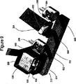
図9は、実施形態による図2から図8の統合型フォトニクスモジュールの主要光学構成要素の一部の整列を示す図である。構成要素は、上述したとおりである。統合型フォトニクスモジュールのビーム結合器210における走査ビーム出射面212が、示されている。
FIG. 9 is a diagram illustrating the alignment of some of the main optical components of the integrated photonics module of FIGS. 2-8 according to an embodiment. The components are as described above. A scanning
図10は、実施形態による図2から図8の統合型フォトニクスモジュールの光学フレーム202の図である。実施形態によれば、光学フレーム202は、ダイキャスティング工程を用いて、アルミニウム、チタンなどの金属から作製されてもよい。あるいは、光学フレーム202は、ガラス充填プラスチックまたは他の寸法安定性のプラスチックなどの射出成形プラスチックから構成されてもよい。任意に、二次機械加工作業は、正確な寸法許容差の提供およびまたは他の設計の好みの達成のために、光学フレームにおいて行われてもよい。他の実施形態によれば、光学フレーム202は、機械加工作業および/またはシート金属形成作業を用いて、作製されてもよい。代替材料および作製工程は、当業者には明白であり、特に明記しない限り、種々の実施形態の範囲内に収まることを意図している。光学フレーム202は、図示されているように、任意に1個部品構成要素または2個部品構成要素であってもよい。任意に、光学フレーム202は、たとえば、プリント回路基板などの多数の構成要素およびその上の構成要素、たとえば、別個の発光体/光学素子/結合器およびスキャナ部分などを含んでもよい。
FIG. 10 is a diagram of the
光学フレーム202は、それぞれの光源206、204および208および関連ビーム形成光学素子を収容するように形成される孔1002、1004および1006を含んでもよい。光学フレーム202はさらに、選択性折り畳みミラー、ビーム結合器などを収容して整列するように形成される1つまたは複数の位置決め面1008(1008a、1008b、1008cおよび1008dが図示されている)を含んでもよい。面1010は、スキャナ(図示せず)を位置合わせして収容するように形成されてもよい。さらに、他の取り付け面および特徴部1012が、他の軸に沿って形成されてもよい。
The
一部の実施形態によれば、光学構成要素は、固締具(たとえば、ねじ、リベットなど)と共に、接着剤、締め付けなどによって、カバー部分(図示せず)を光学フレーム202に機械的に締め付けてもよい。他の実施形態によれば、光学構成要素の1つまたは複数は、個別の固締技術または統合固締技術、接着剤(たとえば、紫外硬化光学接着剤)を用いて、光学フレーム202に機械的に連結されてもよい。実施形態によれば、構成要素が光学フレームに直接的に連結される場合には、別個のカバー部分は排除されてもよい。
According to some embodiments, the optical component mechanically clamps a cover portion (not shown) to the
図11は、実施形態による機械的に連結される回路基板1102を含む統合型フォトニクスモジュールの少なくとも一部分の斜視図である。回路基板110は、任意に、統合型フォトニクスモジュール102の統合型光学エンジン部分114の構造部分を形成してもよい。種々の実施形態によれば、回路基板1102は、センサ、光源ドライバ、スキャナコントローラ、映像コントローラ電子機器およびメモリのうちの1つまたは複数を含んでもよい。上述したように、種々のセンサ、光源ドライバ、スキャナコントローラ、映像コントローラ電子機器およびメモリは、従来のマイクロプロセッサまたはマイクロコントローラおよび関連構成要素、たとえば、1つの統合型ASIC、2つ以上のASIC、2つ以上のASICと1つまたは複数のマイクロプロセッサ(DSPまたは従来のCISCまたはRISCマイクロプロセッサなど)、メモリ(映像メモリICなど)、他の統合構成要素、別個の構成要素およびソフトウェアを含むが、これらに限定されるわけではないさまざまな形態をとってもよい。さらに、映像信号を好ましいフォーマットに変換するために動作可能な媒体モジュールは、コントローラの中および回路基板1102の上に統合されてもよい。MEMSスキャナ120および光源116は、回路基板1102に対して直接的にインターフェイスをとってもよい。
FIG. 11 is a perspective view of at least a portion of an integrated photonics module including a mechanically coupled
図12は、実施形態による統合型フォトニクスモジュールにおける光のビームを走査するように用いられてもよい微小電子機械システム(MEMS)スキャナ618の斜視図である。MEMSスキャナ618は、単結晶シリコンウェーハ1202の層およびパイレックス(登録商標)ガラス1204などの誘電体材料のウェーハの層から形成されてもよく、ウェーハは、従来のシリコン・オン・インシュレータ(SOI)技術に基づいて、密閉的に接合される。層は、水酸化カリウム(KOH)エッチング、深掘り反応性イオンエッチング(DRIE)、その組み合わせなどの技術を用いて、バルクマイクロマシニングの施されたMEMSスキャナを形成するために、部分的におよび完全にエッチングされてもよい。一実施形態によれば、ねじりヒンジおよびミラー走査プレート(以下に記載される)は、所望の共振周波数、エネルギ蓄積、質量、ばね定数などを提供するように調整される薄い構造を形成するように部分的にエッチングされる。
FIG. 12 is a perspective view of a micro electro mechanical system (MEMS)
MEMSスキャナ618は、走査プレートの上の反射金属または誘電性の4分の1波長積層から形成される走査ミラー616を含む。ミラーおよび走査プレートは、ジンバルリング1208からねじり高速走査ヒンジ1206aおよび1206上に懸架されてもよい。ねじり高速走査ヒンジ1206aおよび1206bは、その中心線によって画定される軸を中心にしてジンバルリング1208に対してミラー606の回転を可能にするように動作可能である。ジンバルリングは、今度は、取り付けフレーム1212からねじり低速走査ヒンジ1210aおよび1210b上に懸架される。ねじり低速走査ヒンジ1210aおよび1210bは、その中心線によって画定される軸を中心にして取り付けフレーム1212に対してジンバルリングおよびミラーの回転を可能にするように動作可能である。電磁コイル1214を備えるアクチュエータは、低速走査軸および高速走査軸を中心にした回転を駆動するために、ジンバルリング上に形成される。低速走査波形および高速走査波形の複合体を含む信号は、リード線1216(およびインターフェイスケーブル622、図示せず)を介して、MEMS増幅器(図示せず)を介してMEMSコントローラから受信されてもよい。アクチュエータ1214は、スキャナ磁石620(図示せず、しかし、上記の図では見える)によって形成される外部磁界に対して引張する複合周期的磁界を形成する。
The
ジンバルリング1208が直接的に駆動されるため、低速走査ドライブは、高速走査を励起しうる周波数を排除するように選択される任意の駆動波形を提供してもよい。実施形態によれば、低速走査波形は、60Hzなどのフレーム速度に対応する周期的な周波数で、のこぎり波または非対称の三角波に近似されてもよい。したがって、のこぎり歯状の低速走査波形は、所望の角度による帰線で垂直フレーム走査を行うように動作可能であってもよい。
Because the
高速走査駆動信号は、ミラーおよび走査プレート616の共振周波数に対応するように選択される、たとえば正弦波などの周期的な波形を含む。システムにおけるわずかな非対称性が、高速走査周波数でジンバルリング1208の動きにおける小さな変動を高速走査屈曲部1206aおよび1206bを介して、ミラー616に伝達するように動作可能である。動きにおける小さな変動は、所望の高速走査角度を提供するように、共振によって増幅される。
The fast scan drive signal includes a periodic waveform, such as a sine wave, selected to correspond to the resonant frequency of the mirror and scan
MEMSスキャナ618はさらに、MEMSコントローラへのフィードバックを提供するために、種々のセンサを含んでもよい。これらのセンサとしては、ねじりヒンジ、温度接合部またはサーミスタなどにおける圧電抵抗器(PZR)歪みセンサが挙げられうる。実施形態によれば、ミラーおよび走査プレート616は、ビームクリッピングを生じることなく、複合入力ビームを受信するには十分な約1.2mmの直径を有する。
The
MEMSスキャナ618は、その走査プレートおよび走査ミラー616が1つの非パワー位置または「静止」位置でその上に形成されている状態を示している。実施形態によれば、ミラーは、直流バイアスをアクチュエータに印加することによって、低速走査軸においてパワーの供給された静止位置で傾斜されてもよい。直流バイアスは、低速走査ねじりヒンジ1210a、1210bによって画定される低速走査軸を中心にしてジンバルリング1208に対して名目上の「傾斜」を施してもよい。MEMSスキャナの別の実施形態は、両方の軸において、ミラー616のパワーの供給された静止平面を形成するように動作可能であってもよい。たとえば、MEMSスキャナは、走査プレート上に形成されるアクチュエータ1214によって形成されてもよい。走査プレート上のアクチュエータにおける直流バイアスは、低速走査軸に対して静止傾斜を提供するジンバルリング1208上のアクチュエータ1214に加えて、ねじりヒンジ1206a、1206bによって画定される高速走査軸を中心にして、ミラー616に対して名目上の傾斜を施すように動作可能であってもよい。
The
静止位置におけるそのような名目上の傾斜を用いて、たとえば、ミラー616を統合型光学アセンブリ(図示せず)に対してさらに正確に整列してもよい。
Such a nominal tilt in the rest position may be used, for example, to more accurately align the
図13は、実施形態による統合型フォトニクスモジュール用の3つの用途に対応する3つの構造1302、1304、1306に関して、例示のビーム整形119、125およびビーム整形光学素子602、604、606を示す図である。
FIG. 13 is a diagram illustrating exemplary beam shaping 119, 125 and
ヘッドアップディスプレイに対応する第1の構造1302によれば、ビーム119、125は、統合型フォトニクスモジュールの出力端面212(図示せず)から約100mmの距離で、ウエスト1308に集束されてもよい。種々の実施形態によれば、複数の光源204、206、208から発せられたビームは、図によって示されているように、ビーム結合器210によって変調合成ビームに結合されてもよく、変調合成ビームは、走査変調ビーム125としてビームスキャナ120によって走査されてもよい。100mmの例示の距離は、射出瞳拡大素子(図示せず)の距離に対応しうる。そのような用途において、射出瞳拡大素子は通常、画像が目視者の網膜に投影されうる拡大された射出瞳またはアイボックスを提供するように、最終光学素子126(図示せず)の前に挿入されてもよい。
According to a
携帯型走査ビーム映像プロジェクタに対応する第2の構造1304によれば、ビーム119、125は、統合型フォトニクスモジュールの出力端面212(図示せず)から約500mmの距離で、ウエスト1308に集束されてもよい。種々の実施形態によれば、複数の光源204、206、208から発せられたビームは、ビーム結合器210によって変調合成ビームに結合されてもよく、変調合成ビームは、走査変調ビーム125としてビームスキャナ120によって走査されてもよい。種々の実施形態によれば、図によって示されているように、最終光学素子126は、ビーム経路に配置されてもよい。500mmの例示の距離は、投影表面からの名目上の作動距離に対応しうる。
According to a
頭部装着走査ビームまたは網膜ディスプレイに対応する第3の構造1306によれば、ビーム119は、統合型フォトニクスモジュールの出力端面212(図示せず)から約10mmの距離で、ウエスト1308に集束されてもよい。種々の実施形態によれば、複数の光源204、206、208から発せられたビームは、ビーム結合器210によって変調合成ビーム119に結合されてもよく、変調合成ビームは、ディスプレイの頭部装着部分への透過のために光ファイバ内を進む。10mmの例示の距離は、統合型フォトニクスモジュールの出力端面と、光ファイバ入力結合器との間の距離に対応しうる。種々の実施形態によれば、光ファイバは、単一モード光ファイバであってもよく、変調合成ビーム119を目視者の目の付近にある遠位端部に搬送する。光は通常、入力端部または近位端部でビームによって構成される収束角度に実質的に対応する発散角度で光ファイバの遠位端部から出射してもよい。光ファイバ(図示せず)の遠位端部から出射する光は、目視者の目までの距離に対応する距離に集束され、遠方位置に取り付けられるビームスキャナ(図示せず)によって周期的なパターンで走査され、最終光学素子(図示せず)によって目視者の目までリレーされてもよい。
According to a
図13の図から引き出されうる1つの一般的な見解は、統合型フォトニクスモジュールが種々の用途において動作するように適合されてもよいことである。さらにまたはあるいは、統合型フォトニクスモジュール設計の変形は、種々の用途に適合されてもよく、その一部が、図13に示されている。図14から図18および本願明細書における他の説明は、文字通りかつ固有であり、一部の用途に一連の範囲の用途にわたって共通点または設計の共通点を有する統合型フォトニクスモジュールを提供することを示している。 One general view that can be drawn from the diagram of FIG. 13 is that the integrated photonics module may be adapted to operate in various applications. Additionally or alternatively, variations of the integrated photonics module design may be adapted for various applications, some of which are shown in FIG. 14-18 and other descriptions herein are literally unique and provide an integrated photonics module that has some common or design commonality across a range of applications for some applications. Show.
図14は、実施形態による統合型フォトニクスモジュールに関してビーム整形光学素子の別個の変形および統合型変形を示す図である。ヘッドアップディスプレイ用途1302は、実施形態によれば、円偏光レンズ1402の一部またはすべて、平行光線化レンズ1404、トップハットレンズ1406および集束レンズ1408を用い、そのビームを整形してもよい。任意の円偏光レンズ1402は、非点収差補正を行い、2つの軸のそれぞれにおいて異なる発散を有しうる多くのレーザの出力を、任意の軸において実質的に等しい発散を備えた半径方向に対称のビームに変換してもよい。そのようなレンズは、光パワーの最小の損失で円偏光を提供してもよい。さらにまたはあるいは、クリッピングアパーチャが、システムにおいて用いられてもよい。平行光線化レンズ1404は、トップハットレンズ1406への導入のために実質的に平行な側面を有するビーム形状を提供する。トップハットレンズ1406は、入力ビームのガウスエネルギ分布を、その断面にわたって実質的に等しいパワーを有するトップハット形状の出力ビームに変換する。集束レンズ1408は、上述したようにビームを作動距離に集束する。
FIG. 14 is a diagram illustrating separate and integrated deformations of the beam shaping optics for an integrated photonics module according to an embodiment. The head-up
トップハットビームは、トップハットエネルギ分布に戻るように畳み込む前に、正弦波形状のエネルギ分布によって畳み込む。したがって、見える距離で畳み込まれたトップハット関数を生成するようにトップハットレンズ1406に関する焦点距離を選択することが望ましい場合がある。集束レンズ1408の焦点距離は、EPEでウエストを生成するように選択されてもよく、たとえば、正しい順序で並べられたマイクロレンズアレイ(MLA)であってもよい。EPEは、映像画像が目視者の網膜によって受信される拡大領域を生成するために、遠視野にビームレットを生成する。トップハット形状の複合走査ビームを選択することによって、EPEによって生成されたビームレットもまた、(正弦エネルギ分布を介した畳み込み後)所望の見える距離の範囲内で、トップハット形状であってもよい。トップハット形状のビームレットは、互いを有する「タイルを成し(tile)」、アイボックスにわたってパワーにおける目に見える変動を低減または削減する。
The top hat beam is convolved with a sinusoidal energy distribution before being folded back to the top hat energy distribution. Accordingly, it may be desirable to select a focal length for the
図14の上の図によって表されるHUD用途1302において分かるように、円偏光レンズ1402、平行光線化レンズ1404、トップハットレンズ1406および集束レンズ1408は、1つまたは複数の統合型レンズ1410に結合されてもよい。
As can be seen in the
携帯型プロジェクタの用途1304は、実施形態によれば、円偏光レンズ1402および集束レンズ1408の一部またはすべてを用いて、そのビームを整形してもよい。HUD用途1302と同様に、任意の円偏光レンズ1402は、非点収差補正を行い、2つの軸のそれぞれにおいて異なる発散を有しうる多くのレーザの出力を、任意の軸において実質的に等しい発散を備えた半径方向に対称のビームに変換してもよい。そのようなレンズは、光パワーの最小の損失で円偏光を提供してもよい。さらにまたはあるいは、クリッピングアパーチャが、システムにおいて用いられてもよい。集束レンズ1408は、上述したようにビームを作動距離に集束する。任意に、平行光線化レンズおよびトップハットレンズなどの他のレンズもまた、携帯型プロジェクタの実施形態において用いられてもよい。
図14の真ん中の図によって表される携帯型プロジェクタ用途1304において分かるように、円偏光レンズ1402および集束レンズ1408は、1つまたは複数の統合型レンズ1412に結合されてもよい。
As can be seen in the
頭部装着型ディスプレイの用途1306は、実施形態によれば、円偏光レンズ1402および集束レンズ1408の一部またはすべてを用いて、そのビームを整形してもよい。HUD用途1302および携帯型プロジェクタ用途1304と同様に、任意の円偏光レンズ1402は、非点収差補正を行い、2つの軸のそれぞれにおいて異なる発散を有しうる多くのレーザの出力を、任意の軸において実質的に等しい発散を備えた半径方向に対称のビームに変換してもよい。そのようなレンズは、光パワーの最小の損失で円偏光を提供してもよい。さらにまたはあるいは、クリッピングアパーチャが、システムにおいて用いられてもよい。集束レンズ1408は、上述したようにビームを作動距離に集束する。任意に、平行光線化レンズおよびトップハットレンズなどの他のレンズもまた、頭部装着型ディスプレイの実施形態において用いられてもよい。
The head mounted
図14の下の図によって表される頭部装着型ディスプレイ用途1306において分かるように、円偏光レンズ1402および集束レンズ1408は、1つまたは複数の統合型レンズ1414に結合されてもよい。
As can be seen in the head mounted
統合型レンズ1416は、上述した統合型レンズ1410、1412および1414の物理的な実施形態を代表している。
The
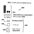
図15から図17は、複数の光学素子にわたってビーム整形機能を分配することによって、種々の用途に用いられうる統合型フォトニクスモジュールの少なくとも共通の部分を提供するための手法を表している。図15は、実施形態による携帯型走査ビームプロジェクタ1502に関する統合型フォトニクスモジュールの部分を示す図である。光源116からのビームは、ビーム整形光学素子602、604および606によって整形され、ビーム結合器210によって結合されて、上述したように変調合成ビーム119を形成する。
FIGS. 15-17 represent a technique for providing at least a common portion of an integrated photonics module that can be used in various applications by distributing beam shaping functions across multiple optical elements. FIG. 15 is a diagram illustrating a part of the integrated photonics module related to the portable
図16は、実施形態による特に図13によって示されているような異なるビーム形状要件を有するHUD1602に関する統合型フォトニクスモジュールの一部を提供するために、図15の携帯型プロジェクタ1502の統合型フォトニクスモジュール部分の使用を示す図である。図16に示されているように、統合型フォトニクスモジュール部分1502は、合成ビーム整形光学アセンブリ1604と結合してもよい。具体的な実施形態によれば、統合型フォトニクスモジュール部分1502は、図13によって示されているように、たとえば、約500mmのウエスト距離を有するビームを有する携帯型走査ビーム映像プロジェクタに適した特性を有する変調合成ビームを提供するように動作可能である。ビームは次に、平行光線化レンズ1404、トップハットレンズ1406およびカラーバランス集束光学素子1606を含む一連のレンズに導入されてもよい。光学アセンブリ1604としての組み合わせにおいて言及された一連のレンズ1404、1406および1606は、携帯型走査ビーム映像プロジェクタに適した形状のビームからHUDに適した形状、たとえば、トップハットパワー分布および100mmの集束距離を有する形状に変換するように構成される。
16 provides an integrated photonics module of the
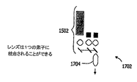
図17は、実施形態によるHUDの場合の統合型フォトニクスモジュール1702を形成するために、複合レンズ1704への光学アセンブリ1604の統合を示す図である。
FIG. 17 is a diagram illustrating the integration of the
図18は、実施形態による任意の適応光学素子の光透過経路および配置を示す統合型フォトニクスモジュール114の少なくとも一部分の斜視図である。統合型フォトニクスモジュール114は、携帯型走査ビーム映像プロジェクタ用に構成された部分1502と、部分1502からの変調合成ビームを受信して、異なる特性を有する変調合成ビーム119を生成するように構成された適応光学素子1704と、を含む。実施形態によれば、部分1502および適応光学素子1704は、ヘッドアップディスプレイ用に構成された統合型フォトニクスモジュール1702の一部分を備える。上述したように、変調合成ビームは、スキャナ120によって周期的なパターンにおいて走査され、変調走査ビーム125を形成する。この実施例では、変調走査ビーム125は、モジュール114を含む統合型フォトニクスモジュールを備えるHUDを装備した車両の運転者に映像画像を提供するように動作可能である
FIG. 18 is a perspective view of at least a portion of the
図19は、実施形態による統合型フォトニクスモジュールの少なくとも一部分の光源204、206および208およびビーム結合器210の関係を示す図である。図19は、別個のR光ビーム1902、G光ビーム1904およびB光ビーム1906を1つの複合光ビーム119に結合するためのビーム結合器210の側面図と、実施形態によるRGBビーム源114の図を含む。
FIG. 19 is a diagram illustrating the relationship between the
ビーム結合器210は、3つのセクション1908、1910および1912を含み、これらのセクションは、共に接合され、光学用途に適したガラスまたはポリマーなどの透明材料から構成される。結合器210はまた、3Wの長さと、X−Z平面における矩形の断面と、を有する入力端面1914を含み、Wの高さと、Y−Z平面における正方形の断面と、を有する出力端面1916を含む。一実施形態において、W=5.5ミリメートル(mm)であり、他の実施形態において、W=3.5mmである。入力端面1914および出力端面1916はいずれも、平坦な光学品質表面である。結合器210の作製は、「APPARATUS AND METHOD FOR COMBINING MULTIPLE ELECTROMAGNETIC BEAMS INTO A COMPOSITE BEAM」という名称の米国特許出願番号第10/828,876号に記載される。この特許は、本発明の譲受人に譲渡され、本願明細書において参照によって援用される。
第1のセクション1908は、高さおよび幅がWであるX−Y平面における平行四辺形形状の断面を有し、セグメント入力端面1918を含む。セグメント入力端面1918は、結合器入力端面1914の部分と、Rビーム1902を結合器出力端面1916に向かって反射するための反射体面608と、を形成する。一実施形態において、面608は、従来の光学コーティングを適用することによって反射性に構成される。ビーム結合器システムの変数に基づいて、このコーティングの反射特性および透過特性を選択することができる(他のコーティングについては、以下に記載する)。入力端面1918と反射体面608との間の角度αは、鋭角である。好ましい実施形態において、α=45°であり、Rビーム1902がWに等しいX次元における最大幅を有することを可能にする。すなわち、α=45°である場合には、幅WのRビームのすべての部分は、Rビームが入力端面1918と適切に整列される限り、反射体面608の上に投影される。しかし、結合器210がW未満の幅を有するRビーム1902用に設計される場合には、反射性である面608の領域は、Rビームが当たる領域に制限されることができる。あるいは、角度αは、45°を超えるように形成されることができる。しかし、角度αは、セグメント1908、1910および1912のすべてに関して同一であるため、αの値を変更する前に、他のセグメント1910および1912に及ぼす影響を考慮する必要がある。さらに、αが45°に等しくない場合には、ビーム源114からのRビームの角度は、反射されたRビームが出力端面1916に対して垂直のままであるように調整される。
The
同様に、第2のセクション1910は、高さおよび幅がWであるX−Y平面における平行四辺形形状の断面を有し、セグメント入力端面1920を含む。セグメント入力端面1920は、結合器入力端面1914の部分を形成し、セクション1908とセクション1910との間の境界に沿って置かれ、反射されたRビーム1902を通過し、Gビーム1904を結合器出力端面1916に向かって反射する反射体面610を含む。一実施形態において、面608は、面610および面610との境界であるセクション1908の面のいずれかまたは両方に対して、従来の光学コーティングを適用することによって反射性に構成される。入力端面1920と反射体面610との間の角度αは、鋭角であり、好ましくは、α=45°であり、Gビーム1904がWに等しいW次元における最大幅を有することを可能にする。しかし、結合器210がW未満の幅を有するGビーム1904用に設計される場合には、反射性である面610の領域は、Gビームが当たる領域に制限されることができる。あるいは、角度αは、45°を超えるように形成されることができる。しかし、角度αは、セグメント1908、1910および1912のすべてに関して同一であるため、αの値を変更する前に、他のセグメント1908および1912に及ぼす影響を考慮する必要がある。さらに、αが45°に等しくない場合には、ビーム源114からのGビームの角度は、反射されたGビームが出力端面1916に対して垂直のままであるように調整される。
Similarly, the
第3のセクション1912は、X−Y平面における三角形形状の断面を有し、結合器出力端面1916およびセグメント入力端面1922を含む。セグメント入力端面1922は、Wの幅を有し、結合器入力端面1914の部分と、セクション1910とセクション1912との間の境界に沿って置かれ、反射されたRビーム1902およびGビーム1904を通過し、Bビーム1906を結合器出力端面に向かって反射する反射体面612と、を形成する。一実施形態において、面612は、面612および面612との境界であるセクション1910の面のいずれかまたは両方に対して、従来の光学コーティングを適用することによって反射性に構成される。入力端面1922と反射体面612との間の角度αは、鋭角であり、好ましくは、α=45°であり、Bビーム1906がWに等しいX次元における最大幅を有することを可能にする。しかし、結合器210がW未満の幅を有するBビーム1906用に設計される場合には、反射性である面612の領域は、Bビームが当たる領域に制限されることができる。あるいは、角度αは、45°を超えるように形成されることができる。しかし、角度αは、セグメント1908、1910および1912のすべてに関して同一であるため、αの値を変更する前に、他のセグメント1908および1910に及ぼす影響を考慮する必要がある。さらに、αが45°に等しくない場合には、ビーム源114からのBビームの角度は、反射されたBビームが出力端面1916に対して垂直であるように調整される。さらに、セクション入力端面1922と出力端面1916との間の角度βは、好ましい実施形態において、実質的に直角である。
The
図20は、実施形態2001による統合型フォトニクスモジュールの少なくとも一部分における光透過を示す図である。光源116は、3つの光源204、206および208を含んでもよく、変調光のビームをそれぞれのビーム整形光学素子602、604および606を介してビーム結合器210に向かって放つように構成される。光源は、光の偏光ビームを発するように構成されてもよい。あるいは、ビーム整形光学素子602、604および/または606は、図示されているように、ビーム結合器210のS偏光を提供するように構成される偏光子を含んでもよい。任意に、ミラー608、610および612は、入射ビームのS偏光成分を結合し、P偏光成分が光トラップ(図示せず)を通過するように構成されてもよい。ビーム結合器のそれぞれのミラー608、610および612は、発光体206、204および208からの変調光のビームをS偏光の変調合成ビーム119に結合する。適応光学素子1704は任意に、ビーム結合器の出力端面1916から光を受信するために、ビーム経路に挿入されてもよい。
FIG. 20 is a diagram illustrating light transmission in at least a portion of the integrated photonics module according to the
偏光ビームスプリッタを備える選択性折り畳みミラー614は、変調合成ビーム119をスキャナ120のミラー616に向かって指向する。選択性折り畳みミラー614は、名目上のミラー(中心と交差する)位置に対して実質的に垂直な方向から走査ミラー616に向かって合成ビームを放つように整列されてもよい。そのような配置は、走査ビームにおける幾何的な歪曲収差を最小限に抑えるために有用である可能性がある。
A
ビーム結合器210におけるS偏光を提供する代わりとして、ビームの偏光の一部またはすべてが、 偏光ビームスプリッタ614によって提供されてもよく、偏光ビームスプリッタは、変調合成ビーム119のS偏光成分を走査ミラー616に向かって指向し、光のP偏光成分を光トラップ(図示せず)を通過させるように動作する。
As an alternative to providing S polarization in
偏光ビームスプリッタ614は、S偏光を優先的に反射するように構成され、したがって、S偏光をスキャナ120に向かって反射する。S偏光変調合成ビームは、走査ミラー616に向かうその経路上にある偏光回転子2002を通過する。偏光回転子は、4分の1波長板として構成されてもよく、走査ミラー616に衝突前にS偏光を円偏光に変換するように動作する。上述したように、スキャナ120は、光125の走査変調ビームを生成するために、視野にわたって周期的パターンにおいてビームを走査するように動作可能である。スキャナミラー616によって反射(および走査)された後、走査ビームは再び、偏光回転子2002を通過する。偏光回転子は、走査ミラーからの現在円偏光のビームをP偏光に変換する。
The
P偏光は、偏光ビームスプリッタ614に向かって伝搬する。偏光ビームスプリッタ614は、P偏光を優先的に通過するように構成され、したがって、P偏光の走査ビーム125がFOVに向かって通過することを可能にする。
P-polarized light propagates toward the
偏光を用いる代わりとして、図20のシステムは、非偏光または楕円偏光を用いてもよい。そのような別の実施形態において、折り畳みミラー614は、半透鏡などの選択性反射体を含んでもよい。衝突ビーム119の一部分は、折り畳みミラー614を通過して、たとえば、光トラップ(図示せず)に向かい、光エネルギの一部分は、スキャナミラー616に向かって指向される。偏光回転子は、別の実施形態において割愛されてもよい。走査ビーム119は、再び半透鏡614に衝突し、その一部分が、FOVに向かって通過する。反射された部分は、光源に向かって戻るか、および/または光トラップに向かって反射してもよい。
As an alternative to using polarized light, the system of FIG. 20 may use unpolarized or elliptically polarized light. In another such embodiment, the
図20の構造に対して複数の別の実施形態が、可能である。図21は、別の実施形態2101による光透過を示す図であり、斜角で、合成ビーム119をスキャナ120に向かって放つ。走査ビーム125は、図20の手法に比べて、ある程度の量のキーストーン歪曲収差を有するパターンにおいてFOVに向かって通過する。一部の実施形態によれば、変調合成ビーム119は偏光される必要はなく、走査ビームが折り畳みミラーを再び通過しない場合には、折り畳みミラー614は、選択性反射体である必要はない。
Several alternative embodiments are possible for the structure of FIG. FIG. 21 is a diagram illustrating light transmission according to another
図22は、スキャナ120がビーム結合器の光源116とは対向する側に位置するように構成される実施形態2201を示す。したがって、光の走査ビームは、光源116の「後方」の方向においてFOVに向かって通過する。
FIG. 22 shows an
図23は、折り畳みミラーは、固体光学素子として構成される偏光ビームスプリッタを備えてもよい実施形態2301を示す図である。
FIG. 23 shows an
図24は、折り畳みミラー614がビーム結合器210に統合される実施形態2401を示す図である。示された実施形態は、偏光ビームスプリッタとして折り畳みミラー614を示す。上述したように、折り畳みミラーは、光の第1の偏光をスキャナ120に向かって反射する。偏光回転子2002は、スキャナ120の2回通過において、偏光を90°回転するように構成され、入射エネルギをスキャナに向かって優先的に反射し、走査ビームをFOVに向かって優先的に通過させる。
FIG. 24 shows an
実施形態2401は、ビーム結合ミラー608、610および612の平面に対して平行な平面に構成される折り畳みミラー614を用いる。
図25Aは、折り畳みミラー614がビーム結合器210に統合される別の実施形態2501を示す図である。実施形態は、光源116に対して前方方向に、走査ビーム125を出射する構造を有する。折り畳みミラー614の平面は、結合ミラー608、610および612の平面に対して実質的に直角であるように構成される。
FIG. 25A shows another
図25Bは、非画像形成検出器を含む統合型フォトニクスモジュールの少なくとも一部分を含む実施形態2502を示す図である。実施形態2502は、任意の光拡散体2506、任意のスペーサ2508、任意の反射側壁2510および非画像形成光検出器2512を備えうる光検出モジュール2504を含む。上述したように、P偏光走査ビーム125は、任意に、非変調であるように構成されてもよく、FOVにわたって走査される。走査ビーム125の一部分は、散乱光2514としてFOVにおける物体から散乱されてもよい。通常、非鏡面物体である場合には、散乱光2514は、非偏光または楕円偏光であってもよい。散乱光は通常、選択性折り畳みミラー614を実質的に充填する平行光線または発散光線の束として形成されてもよい。選択性折り畳みミラー614は、散乱ビーム2514を受信し、そのS成分偏光を任意の光拡散体2506に向かって図示されているように反射する。任意の光拡散体2506は、図示されているように、散乱角にわたって受信光線を散乱するように構成される。散乱光線は、スペーサ2508を通って進み、光検出器2512に衝突する。散乱光線の一部分は、検出器によって受信されることがありえない角度で散乱されてもよい。任意の反射側壁2510は、そのような「消失」エネルギを検出器2512に向けて再指向するために用いられてもよい。検出器2512は、たとえば、光源の放射波長に対応する波長を受信するように構成されてもよく、受信した光エネルギを電気信号に変換するように動作可能である。実施形態によれば、統合型フォトニクスモジュール2502は、FOVからの対応する赤色散乱光、緑色散乱光および青色散乱光を受信するためにフィルタリングされる検出器2512を用いて、複合走査ビーム125として赤色レーザ光、緑色レーザ光および青色レーザ光を発するように構成されてもよい。
FIG. 25B illustrates an embodiment 2502 that includes at least a portion of an integrated photonics module that includes a non-imaging detector. Embodiment 2502 includes a
動作中、検出器2512からの電気信号は、FOVの映像画像を生成するように走査する画素によって、同期的に読み出されてもよい。
In operation, the electrical signal from the
1つまたは複数の任意の検出器2516は、任意に、1つまたは複数の集光レンズを通じて、FOVからのP偏光成分を受信するように構成されてもよい。ビーム結合器210のミラー608、610および612が、波長選択性ミラーであるように構成される場合には、任意の検出器2516によって受信される信号は、FOVからの光を受信し、走査ビームに起因しない対応する電気信号を生成するように動作可能であってもよい。そのような光を用いて、たとえば、FOVにおける周辺照明を決定してもよく、これは今度は、発光体に関する明度、カラーバランスなどを決定してもよい。
One or more
図25Cは、焦点平面検出器アレイを含む統合型フォトニクスモジュールの少なくとも一部分を含む実施形態2503を示す図である。実施形態2503は、レンズまたはレンズ系2520、アパーチャ2522、スペーサブロック2524および焦点平面検出器アレイ2526、たとえば、CCDまたはCMOSの画素化アレイなどを備えうる光検出モジュール2518を含む。
FIG. 25C illustrates an
上述したように、P偏光走査ビーム125は、任意に非変調であるように構成されてもよく、FOVにわたって走査される。走査ビーム125の一部分は、散乱光2514としてFOVにおける物体から散乱されてもよい。通常、非鏡面物体である場合には、散乱光2514は、非偏光または楕円偏光であってもよい。散乱光は通常、選択性折り畳みミラー614を実質的に充填する平行光線または発散光線の束として形成されてもよい。選択性折り畳みミラー614は、散乱ビーム2514を受信し、そのS成分偏光をレンズ2520に向かって図示されているように反射する。レンズ2520およびアパーチャ2522は、スペーサ2524の遠い方の表面に共役像平面を形成するように構成される。焦点平面検出器アレイ2526は、FOVの共役像を検出し、対応する電気信号に変換するように動作可能である。動作中、焦点平面検出器アレイ2526は、たとえば、スキャナのフライバック周期中に、映像フレーム速度で読み出されてフラッシュされ、FOVの映像画像を生成してもよい。
As mentioned above, the P-polarized
図示されているように、このように画像形成される光は、選択式折り畳みミラー614による反射のために選択されたS偏光から形成されてもよい。あるいは、検出経路の4分の1波長板(図示せず)などの偏光回転子が、たとえば、レンズ2520とアパーチャ2522との間に含まれて、平面偏光を円偏光に変換してもよい。そのような手法は、たとえば、焦点平面検出器2526に関連する偏光依存許容効果を回避するために好都合である場合がある。
As shown, the light imaged in this way may be formed from S-polarized light selected for reflection by the
あるいは、図25Bおよび図25Cの実施形態を示すために、検出器2512または2526は、選択性折り畳みミラー614からの散乱光を受信するのではなく、FOVからの散乱光を直接的に受信するように構成されてもよい。
Alternatively, to illustrate the embodiment of FIGS. 25B and 25C,
図25Bおよび図25Cのそれぞれの具体的な実施形態のサブシステム2504または2518などの光検出サブシステムを含む用途の場合には、システムのコントローラ部分は、当然のことながら、検出器からの電気信号を受信し、アナログ信号をディジタル信号に変換し(または統合型ADCを用いて、検出器向けのディジタル信号を単に受信し)、受信信号を映像画像の中に集め、受信した画像を復号化バーコードまたはOCRのデータなどの対応するデータに復号化するか、または他の方法で受信信号を処理して、用途に応じた機能を実現するように構成されて動作可能であってもよい。
For applications that include a light detection subsystem, such as
一部の実施形態は、検出器2512、2526からの信号を用いて、光源励起の深さおよび/またはタイミングを修正し、走査変調ビーム125を修正し、たとえば、投影表面の非均一性、距離および/または周辺照明を補償してもよい。そのような補償を行うための一部の実施形態は、「PROJECTION DISPLAY WITH SCREEN COMPENSATION」という名称の米国特許出願第11/284,043号に開示されており、参照によって本願明細書に援用される。
Some embodiments use the signals from the
他の実施形態は、検出器2512、2526からの信号を用いて、たとえば、ビームスキャナの移動と光源との位相関係を修正することによって、統合型フォトニクスモジュールと投影表面との間の相対的な移動を補償してもよい。補償を行うための一部の実施形態は、「PROJECTION DISPLAY WITH MOTION COMPENSATION」という名称の米国特許出願第11/635,799号に開示されており、参照によって本願明細書に援用される。
Other embodiments use the signals from the
図25Dは、図25Aの実施形態2501に対応するが、スキャナ120が移動され、選択性折り畳みミラー614が、変調合成ビームを通過させるが走査ビーム125を反射するために、90°に向けられる点が異なる実施形態2527である。S偏光を有する変調合成ビーム119の少なくとも一部分は、ビーム結合器210から放たれ、選択性折り畳みミラー614を通過し、偏光回転子2002を通過して、スキャナ120のミラー616に衝突する。選択性折り畳みミラー614は、変調合成ビーム119の角度に対応する角度で、平面偏光を通過するが、直交する偏光角で平面偏光を反射するように整列される。光回転子2002は、複合変調ビーム119の偏光を走査ミラー616までの途中で円偏光に回転する。走査ミラー616は、偏光回転子2002によって周期的な走査パターンにおいて、光の受信ビームの反射を走査する。偏光回転子は、ビーム結合器210から放たれるときに、変調合成ビーム119の配向から実質的に90°の配向で、円偏光から平面偏光に走査ビームの偏光を回転する。選択性折り畳みミラー614は、走査ビーム125として視野に向かって回転された走査ビームを反射する。図25Dの実施例において、走査ビーム125は、S偏光を有する。
FIG. 25D corresponds to the
図25Eは、実施形態による統合型フォトニクスモジュール2529の少なくとも一部分の光透過を示す図であり、ビームスキャナは、名目上の画像投影方向に対して垂直以外の平面にある。図25Aの実施形態と同様に、偏光選択性折り畳みミラー614は、たとえば、偏光ビームスプリッタとして構成されてもよく、示された方向において、光の変調合成ビームを偏光回転子2002に向かって指向するように構成される。偏光回転子を通過後、光の変調合成ビームは、垂直折り畳みミラー2530によって、ビーム走査アセンブリ120(ミラー2530によって部分的に見えない)に向かって指向され、走査ミラー(図示せず)に衝突する。走査光は次に、ミラー2530から反射され、偏光ビームスプリッタ2002を通り、その回転偏光のために、選択性折り畳みミラー614を通過して、走査ビーム125として視野に達する。一実施形態によれば、走査ミラーは、名目上図の平面内にあり、したがって名目上の映像投影軸に対して平行な平面にあるように構成されてもよい。この手法は、中でも、走査アセンブリ120の永久磁石が、厚さ寸法においてより小さな外寸を有することを可能にすることによって、図に対して垂直な次元においてより薄いパッケージを提供しうる。折り畳みミラー2530は、たとえば、第1の表面金属であってもよく、誘電体であってもよく、または少なくとも光源116の出射波長に対応する波長に関して、それに衝突する実質的にすべての光を反射する他のミラーであってもよい。当然のことながら、偏光回転子2002の位置は、垂直折り畳みミラー2530とスキャナミラー(図示せず)との間にあるなど、可変であってもよい。
FIG. 25E is a diagram illustrating light transmission of at least a portion of the integrated photonics module 2529 according to an embodiment, where the beam scanner is in a plane other than perpendicular to the nominal image projection direction. Similar to the embodiment of FIG. 25A, the polarization-
図26は、光源204の1つがそのビームをビーム結合器210の端部から放つように構成される別の実施形態2601を示す図である。図示されているように、そのビームは、ビーム整形光学素子602によって折り畳みミラー614およびスキャナ120の端部に対向する端部に放たれる。実施形態2601は、物理的に大きい光源204が用いられる場合に特に好都合である場合がある。
FIG. 26 shows another
図27は、実施形態による統合型フォトニクスモジュールの少なくとも一部分を含むスキャナコントローラ122を含むブロック図2701である。
FIG. 27 is a block diagram 2701 including a
図27の実施形態によれば、スキャナコントローラ122は、スキャナ制御ASIC2702と、コプロセッサとして動作可能であるディジタル信号プロセッサ(DSP)2704と、電源回路およびメモリを含む支援回路と、プリント回路基板におけるフレックス回路相互接続と、を含む。図27の実施形態は、制御機能性のより大きな部分が、スキャナ制御ASICに統合される図1のスキャナコントローラ122に比べて、統合の程度が若干低減していることに留意されたい。種々の実施形態によれば、動作の一般的な理論は、類似であってもよい。
According to the embodiment of FIG. 27, the
スキャナコントローラ122は、コントローラ相互接続2706にわたって映像コントローラ電子機器106(図27には示さず)に対して適切なタイミング情報を提供すると同時に、2軸MEMSスキャナを駆動するように動作可能である。スキャナコントローラ122はさらに、周辺光レベルを監視して、自動位相較正パルスを処理し、任意に映像コントローラ電子機器にこれらの測定値をリレーするように動作可能であってもよい。
記載して図12に図示したように、1つのスキャナの実施形態は、2軸における磁気ドライブと、両軸用のPZRセンサを備えたMEMSスキャナを含む。 As described and illustrated in FIG. 12, one scanner embodiment includes a MEMS scanner with a magnetic drive in two axes and a PZR sensor for both axes.
一部の実施形態によれば、スキャナコントローラ122は、統合型フォトニクスモジュールの光学エンジン部分114(図示せず)付近に物理的に取り付けられてもよい。上述したような頭部装着型ディスプレイなどの一部の実施形態によれば、スキャナコントローラ122は、スキャナ付近の遠方位置にあってもよく、光源116(図示せず)およびビーム結合器の少なくとも一部分およびビーム整形光学素子118(図示せず)とは物理的に分離してもよく、光源およびビーム整形光学素子は、近方位置から光ファイバを介して遠方位置までMEMSスキャナ618のミラーに光を提供するように構成される。同様に、映像コントローラ電子機器106(図示せず)は、光源およびビーム整形光学素子付近に近接して取り付けられてもよく、電気、無線または光学インターフェイス2706を介して遠方に取り付けられたスキャナコントローラ122と通信してもよい。そのような実施形態において、コンパクトなパッケージにおいて統合型フォトニクスモジュールの近方部分に取り付けることが適切である場合があり、ユーザのベルトで支えられてもよく、頭部装着パッケージにおいてシステムの遠方部分に取り付けられてもよい。
According to some embodiments, the
実施形態によれば、DSP2704は、「CIRCUIT FOR DRIVING A PLANT AND RELATED SYSTEM AND METHODS」という名称の米国特許出願第11/266,584号(参照によって本願明細書に援用される)に開示された方法に基づいて、低速走査の同調および能動的減衰を提供するために低速走査高速フーリエ変換(FFT)処理を提供してもよい。さらに、DSP2704は、映像コントローラ電子機器とのデータ通信、MEMSスキャナに関する較正データを入力するためのインターフェイスの提供、MEMS動作、自動位相結果、映像コントローラ電子機器に対する正常動作中に、周辺光センサ2707から受信した周辺輝度、温度センサ2708から受信した温度などに関連する変数の供給、ファームウェアおよびソフトウェアのフィールドアップグレードのためのインターフェイス、重要な動作の適正なタイミングを確保するためのタスクスケジューリング、高速走査発振器レジスタの初期化および調整、PZRセンサの開ループ温度補償のうちの1つまたは複数をはじめとする機能性を提供してもよい。
According to an embodiment,
実施形態によれば、スキャナドライブASIC2702は、MEMS制御を行い、自動的位相(自動位相)相関を行うように動作可能である混合信号(アナログおよびディジタル)デバイスであってもよい。スキャナドライブASIC2702は、2軸MEMSスキャナ618を駆動および制御することができる。2軸MEMSスキャナ618は、圧電抵抗(PZR)フィードバックセンサを有する両方の軸で磁気的に作動されるタイプであってもよい。実施形態によれば、スキャナドライブASIC2702は、たとえば、PZRバイアス回路2709を有するPZRフィードバックセンサに対するユーザがプログラム可能な電流バイアスの提供、プログラム可能な振幅で高速走査軸と自己共振するように動作可能な閉ループ発振器回路2710の提供(AGC変数は、緩速な始動および同調制御オプションを可能にするように調整可能であってもよい)、高速走査共振周波数と同期する低速走査サンプリングクロック(50〜200kHz)を生成するための位相ロックループ(PLL)の提供(多重化係数はプログラム可能であってもよい)、低速走査アナログ・ディジタル変換器(ADC)2712の提供(PZR増幅器からの低速走査入力信号は、DSPプロセッサ2704用のディジタル信号に変換され、ADC解像度は、50〜200kHzのサンプリング速度で、12〜16ビットであってもよい)、低速走査ディジタル・アナログ変換器(DAC)2714の提供(低速走査波形用のディジタル入力信号は、アナログ電圧に変換され、加算回路2716において高速走査駆動信号と加算される)、許容範囲内のミラーの角度を示すミラー状態信号の提供、自動位相センサインターフェイス回路の提供(回路は、自動位相関数用の信号を調整するために、外部光検出器2718と共に動作し、その結果を測定する)、映像コントローラ電子機器と通信し、初期化および監視のために内部レジスタへのアクセスの読み出し/書き込みを可能にするSPIシリアルディジタルインターフェイス2720の提供をはじめとする種々のアナログおよびディジタル機能の一部またはすべてを含んでもよい。
According to an embodiment, the
高速走査発振器ブロック2710は、PZRフィードバック信号を用いて、閉ループ発振器回路を作成する。発振周波数は、スキャナの高速走査軸の共振周波数によって決定される。発振の振幅は、プログラム可能な設定点を有するAGC回路によって制御される。このループからの出力は、他のシステム構成要素を駆動するためのマスタ同期信号を提供するFS共振周波数で方形波であるFS SYNCである。共振周波数は、約5kHz〜40kHzで変化することができる。 Fast scan oscillator block 2710 uses the PZR feedback signal to create a closed loop oscillator circuit. The oscillation frequency is determined by the resonance frequency of the high-speed scanning axis of the scanner. The amplitude of oscillation is controlled by an AGC circuit having a programmable set point. The output from this loop is an FS SYNC that is a square wave at the FS resonance frequency that provides a master synchronization signal for driving other system components. The resonant frequency can vary from about 5 kHz to 40 kHz.
低速走査位置信号は、MEMSスキャナ618における低速走査PZRから受信され、次に低速走査ADC2712において、増幅、フィルタリング、ディジタルへの変換が行われる。このディジタル信号は、解析のためにDSP2704に送信される。DSPは、低速走査DAC2714において、アナログに変換されるディジタルコマンド信号を送り返す。アナログ低速走査駆動信号は、加算回路2716において高速走査出力と加算され、和は、外部パワーアンプ2722に送信される。パワーアンプ2722は、加算されたアナログ信号を増幅して、スキャナ618への駆動電力を提供する。
The slow scan position signal is received from the slow scan PZR in the
自動位相回路2724は、1つまたは複数の外部光検出器2718と共に動作する。走査ビーム125(図示せず)は、周期的に検出器2718を横切る。アナログインターフェイス回路2724は、横切るレーザビームに応じてパルスを生成し、パルス長は、DSP2704に伝送される情報である。
高速走査発振器2710は、アナログ「自己共振」回路であるように設計され、MEMS PZRセンサからの実時間位置情報を取得し、適切な振幅利得および位相遅延を適用し、ミラーのフィードバック信号に基づいてミラーを共振するように駆動する。レジスタを備えたブロックは、SPIプロセッサインターフェイスを介して調整可能であってもよく、MEMS特性を提供して、デバイス間、ロット間および/または設計間の許容差に適合させる。 The fast scan oscillator 2710 is designed to be an analog “self-resonant” circuit, obtains real-time position information from the MEMS PZR sensor, applies appropriate amplitude gain and phase delay, and based on the mirror feedback signal The mirror is driven to resonate. A block with registers may be adjustable via an SPI processor interface to provide MEMS characteristics to accommodate tolerances between devices, lots and / or designs.
図12に関して記載したように、ミラーの高速走査移動は、MEMSスキャナ618におけるダイ屈曲部に組み込まれるPZR歪みセンサによって検知される。PZRセンサには、PZRバイアス回路2709によって調整可能な直流バイアス電流が提供される。バイアス電流は、ソフトウェア制御値または外部抵抗器によってプログラムされてもよい。PZRフィードバック差分検知信号は、調整可能な利得によって低雑音差動前置増幅器2722において増幅される。差動前置増幅器2722の利得は、ソフトウェアによって制御されてもよく、または外部抵抗器によって設定され、所与のミラー角度の偏向に関して(ピーク・ツー・ピーク電圧において)較正信号レベルを提供してもよい。前置増幅器2722の出力は、雑音帯域幅を制限する帯域通過フィルタ2725においてフィルタリングされる。帯域通過フィルタ2725は、低域通過フィルタが後に続く高域通過フィルタを含みうる。帯域通過フィルタ2725の出力信号を用いて、スキャナ制御システムを駆動してもよい。共振において、駆動信号とスキャナの移動との間のには90°の位相のずれがある。閉ループ発振を維持するために、余分な90°の位相のずれが、位相シフタ2726によってループに導入される。位相シフタ2726の出力は、比較器2728において、「正され(squared up)」、ディジタル高速走査同期信号を作成する。高速走査同期信号は、位相ロックループ出力2730によってDSP2704に伝送され、低速走査駆動用のほか、映像コントローラ電子機器106(図示せず)において行われる映像信号処理用の主要時間基準としても用いられてもよい。
As described with respect to FIG. 12, high-speed scanning movement of the mirror is detected by a PZR strain sensor incorporated in the die bend in
自動利得制御(AGC)回路を用いて、きわめて正確な値で、発振振幅を維持してもよい。ループは、振幅検出器、可変利得増幅器およびAGCコントローラを含んでもよい。振幅検出器は、帯域通過フィルタ2725の出力の振幅に比例する直流電圧を生成する。この電圧はAGCコントローラにおける設定点に比較され、比例積分微分(PID)制御アルゴリズムを実装する。PIDコントローラの出力は、可変利得増幅器2732の制御電圧入力として用いられる。
An automatic gain control (AGC) circuit may be used to maintain the oscillation amplitude with a very accurate value. The loop may include an amplitude detector, a variable gain amplifier, and an AGC controller. The amplitude detector generates a DC voltage that is proportional to the amplitude of the output of the
ミラー角度および周波数監視回路2734は、振幅検出器の出力を監視する。振幅がプログラム可能な設定点を超えている場合には、保護回路が、運転停止コマンドを発し、駆動信号を直ちに無効にする。2次安全回路は、駆動信号の振幅を監視し、それがプログラム可能な値を超えないようにする。
A mirror angle and
図28は、実施形態によれば、映像コントローラ106、スキャナコントローラ122およびビームスキャナ618を含む統合型フォトニクスモジュールコントローラ用のブロック図2801である。
FIG. 28 is a block diagram 2801 for an integrated photonics module controller that includes a
映像コントローラ106は、システムリソースからの映像信号の受信、任意に映像メモリにおける受信された映像データの任意のキャッシュ格納、信号のγ補正信号への変換、γ補正信号の等化カラー信号への変換、配線のバッファリング、受信した映像信号における理想的な画素位置の関数として走査ビームによって走査される実際の画素位置の値を決定するための内挿の実行、光源に関する輝度値の決定、光源補償および較正の実行、および画素クロックから受信されたタイミング信号に同期する光源駆動回路に対する補償輝度値の供給(画素クロックは、MEMS制御モジュール122によって提供される水平同期パルスおよび垂直同期パルスによって生成される)のうちの一部またはすべてを行うように動作可能であってもよい。
The
任意に、映像コントローラ106は、受信された映像フォーマットを好ましい映像フォーマットに変換するように動作可能な媒体モジュール2802を含んでもよい。一実施形態によれば、媒体モジュール2802は、受信したアナログ映像信号をディジタル映像信号に変換するように動作可能である。他の実施形態によれば、媒体モジュールは、割愛されてもよく、またはシステムリソースとして統合されてもよい。
Optionally, the
統合型フォトニクスモジュールコントローラ2801の操作性の複数の実施形態の態様が、「CIRCUIT FOR DETECTING A CLOCK ERROR IN A SWEPT−BEAM SYSTEM AND RELATED SYSTEMS AND METHODS」という名称の米国特許出願第11/316,326号、「CIRCUIT FOR DETECTING A CLOCK ERROR IN A SCANNED IMAGE SYSTEM AND RELATED CIRCUITS,SYSTEMS,AND METHODS」という名称の米国特許出願第11/316,683号、「METHOD AND APPARATUS FOR ILLUMINATING A FlELD−OF−VIEW AND CAPTURING AN IMAGE」という名称の米国特許出願第10/630,062号、「APPARATUS AND METHOD FOR BI−DIRECTIONALLY SWEEPING AN IMAGE BEAM IN THE VERTICAL DIMENSION AND RELATED APPARATI AND METHODS」という名称の米国特許出願第10/441,916号、「ELECTRONICALLY SCANNED BEAM DISPLAY」という名称の米国特許出願第10/118,861号、「APPARATUSES AND METHODS FOR UTILIZING NON−IDEAL LIGHT SOURCES」という名称の米国特許出願第10/933,033号、「SCANNED DISPLAY WITH VARIATION COMPENSATION」という名称の米国特許第6,661,393号、および「SCANNED DISPLAY WITH VARIATION COMPENSATION」という名称の米国特許第6,445,362号に開示されており、いずれも、参照によって本願明細書に援用される。
A number of embodiments aspects of the operability of the integrated
図29は、実施形態2901による移動体電子デバイス2902に統合された統合型フォトニクスモジュール102の使用を示す図である。図から分かるように、実施形態は、携帯型電子デバイス2902の上または長い寸法と名目上整列される方向において変調光125の走査ビームを発するように構成される。任意に、統合型フォトニクスモジュール102は、異なる方向または複数の方向において、走査ビームを放つように構成されてもよい。あるいは、統合型フォトニクスモジュール102は、拡散体の後側に画像を投影するように構成されてもよく、したがって、後部投影スクリーンを形成する。
FIG. 29 is a diagram illustrating the use of an
移動体デバイス2902は、バーコードスキャナ、携帯型コンピュータ、パームトップコンピュータ、携帯電話、mp3再生装置などの携帯型音声デバイス、ハードディスクに基づく携帯型音声再生装置、携帯型映像再生装置、ハードディスクに基づく携帯型映像再生装置、ディジタルゲーミングシステム、ビジネスのプレゼンテーション用ポインタ、レーザポインタ、前方投影テレビまたは後方投影テレビなどをはじめとする種々のデバイスタイプを含みうるが、これに限定されるわけではない。
The
図30は、実施形態3001による自動車ヘッドアップディスプレイ用途における統合型フォトニクスモジュールの使用を示す図である。別の実施形態または用途としては、航空機、船舶、モータサイクル用などのHUDが挙げられうる。
FIG. 30 is a diagram illustrating the use of an integrated photonics module in an automotive head-up display application according to
車両3002は、機器クラスタ3006を収容するダッシュボード3004を含んでもよい。機器クラスタは、乗員3010に向かって車両のフロントガラスを含みうるリレー光学素子3008によって走査ビーム画像を投影するように構成される光学部分104を備えた統合型フォトニクスモジュール201を含む。システムは、乗員3010の片目または両目130の位置に対応する射出瞳またはアイボックス3012を提供するように構成されてもよい。
The
そのようなシステムは、低照度前方画像、車両限界情報、地図または運転方向、娯楽コンテンツ、車両3002の位置に任意に関連しうる広告コンテンツ、緊急情報などをはじめとするが、これらに限定されるわけではない種々の情報を目視者に提供するために用いられてもよい。
Such systems include, but are not limited to, low-light front images, vehicle limit information, maps or driving directions, entertainment content, advertising content that may be arbitrarily related to the location of the
図31は、実施形態3101による統合型フォトニクスモジュールを用いた携帯型走査ビーム投影ディスプレイ3102の斜視図である。図31に示されているように、携帯型投影ディスプレイ3102は、実施形態の構造に基づき、ユーザ3010の手に保持されてもよい。出射光学素子3104は、ユーザによって所望であるときに、携帯型映像プロジェクタ3102の本体に関する長手方向に整列された方向3106において走査ビーム125によって画像を投影するように構成されていることが示されている。
FIG. 31 is a perspective view of a portable scanning
別の実施形態によれば、携帯型映像プロジェクタ3102は、制御フィールドを投影または検出してもよい。任意に、ディスプレイの視野は、散乱光検出器などの検出器を用いて、ユーザによって所望であるときに、投影画像の制御など、マウス、ポインタなどを使用するためにフィードバックを可能にするために監視されてもよい。
According to another embodiment,
図31に示されているように、携帯型走査ビーム投影ディスプレイ3102は、実施形態によるその上に取り付けられる出射光学素子3104を有する本体を含みうる。一部の実施形態によれば、出射素子3104は、ある範囲の位置まで回転されてもよい。たとえば、第1の位置において、光学素子は、デバイスの本体によって遮蔽され、デバイスは「オフ」または休眠状態に切り替えられる。光学素子3104の位置は、たとえば、光学復号器、回転スイッチなどを用いて、検知され、自動的にモードを切り換えてもよい。別の例示の位置において、光学素子3104は、テーブル表面を横断するのに適した1つまたは複数の角度で、略前方に画像を投影するように回転されてもよい。投影された画像は任意に、自動的に回転され、その結果、本体の前方に面するユーザによって見られるのに好都合であるようにするために、デバイス3102の本体の基部に向かって「上部」が位置決めされるようになっていてもよい。第3の例示の位置において、光学素子3104は、たとえば、携帯型映像プロジェクタ3102の本体の長軸に対して略垂直であるテーブル表面に対して略前方かつ平行な位置まで回転され、本体がテーブル上に位置決めされると同時に、壁の上に画像を投影してもよい。位置は、壁における画像の高さを選択するために、テーブル面と平行から上向きまたは下向きに調整されてもよい。投影画像は任意に、自動的に回転され、「上部」が壁の上方向に向けられる画像を投影してもよい。
As shown in FIG. 31, a portable scanning
図31に示された第4の位置において、光学素子3104は、携帯型映像プロジェクタ3102の本体の長手軸と略平行な位置まで回転される。このモードでは、画像プロジェクタは、ユーザの手に好都合に保持され、垂直表面または水平表面に向かって向けられると同時に、臨機応変なプレゼンテーションを行うことができる。
In the fourth position shown in FIG. 31, the
上述したように、種々の用途において用いられる統合型フォトニクスモジュールは、画像捕捉機能性を含みうる。捕捉された画像は、種々の機能を実現するために用いられてもよい。たとえば、図29のシステム2901の実施形態の場合には、投影ディスプレイを提供することに加えて、レーザカメラとして機能することが望ましい場合もある。
As mentioned above, integrated photonics modules used in various applications can include image capture functionality. The captured image may be used to implement various functions. For example, in the embodiment of
図30のシステム3001は、捕捉画像の分析を含み、警報起動、システムの運転停止の実行、「自動巡回」への変換、1つまたは複数の車両乗員3010の決定した特性に基づく映像または静止画像の格納などを行ってもよい。たとえば、運転者またはパイロット3010が転寝状態であると決定される場合には、その個人を目覚めさせるために警報を用いてもよい。乗員が未知であり、警報システムが無効または別の方法で干渉されていると決定される場合には、システムは、乗員の画像の捕捉、車両の停止および/または状態の法執行機関への通知などを行いうる。一連の映像フレームの分析により、乗員が酔っている状態である可能性があると決定される場合には、システムは、道路の路肩に車両を誘導して、続いて、障害が問題とならなくなるまで、少なくとも部分的なシステムの運転停止を実行するように乗員に通知してもよい。
The
同様に、システム3001は、検出されたFOVまたは周辺照明などに応じて、ディスプレイ輝度、コンテンツなどを調整してもよい。
Similarly,
既に述べたように、システム3101は、ディスプレイコンテンツを制御するために、捕捉画像に作用してもよい。そのような作用を用いて、たとえば、仮想画像のより大きな部分のようにディスプレイの「パン」、ディスプレイ表面の粗さの補正、ディスプレイ表面と携帯型映像プロジェクタとの間の相対的な移動の補償などを行ってもよい。
As already mentioned,
本発明の前述の概要、図面の簡単な説明および詳細な説明は、読者がより理解しやすいようにすることを意図した態様で、本発明による例示的な実施形態を記載している。他の構造、方法および等価物が、本発明の範囲内にある可能性はある。本願明細書に記載される本発明の範囲は、特許請求の範囲によってのみ制限されるものとする。 The foregoing summary of the invention, brief description of the drawings and detailed description, set forth exemplary embodiments according to the invention in a manner intended to make the reader more understandable. Other structures, methods and equivalents may be within the scope of the invention. It is intended that the scope of the invention described herein be limited only by the claims.
Claims (2)
第1の整列フレームと、
前記第1の整列フレームに取り付けられ、第1の軸に沿って赤色光の変調ビームを発するように動作可能である変調可能な赤色レーザダイオードと、
前記第1の整列フレームに取り付けられ、前記第1の軸に平行な第2の軸に沿って変調した緑色光のビームを発するように動作可能である変調可能な緑色レーザと、
前記第1の整列フレームに取り付けられ、前記第1の軸および前記第2の軸に平行な第3の軸に沿って青色光の変調ビームを発するように動作可能である変調可能な青色レーザダイオードと、
前記第1の整列フレームに取り付けられ、赤色光、緑色光および青色光の前記変調ビームを受信し、前記受信したビームを変調合成ビームに結合し、第4の軸に沿って前記合成ビームを放つように整列されるビーム結合器と、
前記第1の整列フレームに取り付けられ、第5の軸に沿って前記合成ビームを受信するように整列され、周期的な走査パターンにおいて変調走査ビームとして前記合成ビームを偏向するように動作可能であるビームスキャナと、
前記ビーム結合器と前記ビームスキャナとの間に位置し、前記変調合成ビームおよび前記変調走査ビームを受信し、前記変調走査ビームの少なくとも一部分を視野に向かって通過させることを可能にするように整列される選択性反射体と、
前記ビーム結合器と前記ビームスキャナとの間に位置し、前記変調合成ビームおよび前記走査ビームを受信し、前記受信した変調合成ビームの偏光を90°回転させ、且つ、前記走査ビームの偏光を前記ビームスキャナによって受信された前記変調合成ビームから90°の配向にさらに回転させるように整列される偏光回転子と、を備え、
前記第5の軸が前記第4の軸に対して平行であり、前記選択性反射体は、前記受信された変調合成ビームの少なくとも一部分を前記ビームスキャナに向かって通過させ、前記変調走査ビームの少なくとも一部分を前記視野に向かって反射するように構成されることを特徴とする統合型フォトニクスモジュール。An integrated photonics module suitable for integration in electronic devices,
A first alignment frame;
A modulatable red laser diode attached to the first alignment frame and operable to emit a modulated beam of red light along a first axis;
Attached to said first alignment frame, a modulatable green laser is operable to emit green light beam modulated along a second axis parallel to said first axis,
A modulatable blue laser diode mounted on the first alignment frame and operable to emit a modulated beam of blue light along a third axis parallel to the first axis and the second axis When,
Attached to the first alignment frame, receives the modulated beams of red, green and blue light, combines the received beams into a modulated combined beam and emits the combined beam along a fourth axis A beam combiner that is aligned as follows:
Attached to the first alignment frame, aligned to receive the combined beam along a fifth axis, and operable to deflect the combined beam as a modulated scanning beam in a periodic scan pattern. A beam scanner,
Located between the beam combiner and the beam scanner, aligned to receive the modulated combined beam and the modulated scanning beam and allow at least a portion of the modulated scanning beam to pass toward the field of view. A selective reflector,
Positioned between the beam combiner and the beam scanner, receiving the modulated composite beam and the scanning beam, rotating the polarization of the received modulated composite beam by 90 °, and changing the polarization of the scanning beam to the A polarization rotator aligned to be further rotated to a 90 ° orientation from the modulated combined beam received by a beam scanner;
The fifth axis is parallel to the fourth axis, and the selective reflector passes at least a portion of the received modulated combined beam toward the beam scanner, wherein the modulated scanning beam An integrated photonics module configured to reflect at least a portion toward the field of view .
Applications Claiming Priority (3)
| Application Number | Priority Date | Filing Date | Title |
|---|---|---|---|
| US79107406P | 2006-04-11 | 2006-04-11 | |
| US60/791,074 | 2006-04-11 | ||
| PCT/US2007/009145 WO2007120831A2 (en) | 2006-04-11 | 2007-04-11 | Integrated photonics module and devices using integrated photonics modules |
Publications (3)
| Publication Number | Publication Date |
|---|---|
| JP2009533715A JP2009533715A (en) | 2009-09-17 |
| JP2009533715A5 JP2009533715A5 (en) | 2010-03-18 |
| JP4856758B2 true JP4856758B2 (en) | 2012-01-18 |
Family
ID=38480668
Family Applications (1)
| Application Number | Title | Priority Date | Filing Date |
|---|---|---|---|
| JP2009505501A Active JP4856758B2 (en) | 2006-04-11 | 2007-04-11 | Devices using integrated and integrated photonics modules |
Country Status (5)
| Country | Link |
|---|---|
| US (5) | US7834867B2 (en) |
| EP (2) | EP2005763B1 (en) |
| JP (1) | JP4856758B2 (en) |
| CN (5) | CN103458251B (en) |
| WO (1) | WO2007120831A2 (en) |
Families Citing this family (160)
| Publication number | Priority date | Publication date | Assignee | Title |
|---|---|---|---|---|
| US20080136974A1 (en) * | 2004-12-28 | 2008-06-12 | Ning Yuan | Apparatus for Projecting Video Image and Method Thereof |
| US7834867B2 (en) * | 2006-04-11 | 2010-11-16 | Microvision, Inc. | Integrated photonics module and devices using integrated photonics modules |
| WO2007146093A2 (en) * | 2006-06-06 | 2007-12-21 | Microvision, Inc. | Beam scanner with reduced phase error |
| US8810637B2 (en) * | 2007-04-03 | 2014-08-19 | Karl Storz Imaging, Inc. | Universal camera control unit |
| US8031403B2 (en) * | 2007-07-02 | 2011-10-04 | Texas Instruments Incorporated | System and method for reducing visible speckle in a projection visual display system |
| US20090136212A1 (en) * | 2007-11-28 | 2009-05-28 | Klein Scott V | Self contained projection module suitable for retail and method |
| US20090190098A1 (en) * | 2008-01-29 | 2009-07-30 | Microvision, Inc. | Scanned Beam Display Engine with Polarizing Beam Splitter |
| DE102008002809A1 (en) * | 2008-03-21 | 2009-09-24 | Patev Gmbh & Co. Kg | Micromechanical device for e.g. binoculars, has image processing units, and imaging element and position, orientation or movement detecting system that are mechanically and fixedly connected with each other at common component |
| JP5143772B2 (en) * | 2008-03-28 | 2013-02-13 | パナソニック株式会社 | Image display device and image display method |
| US8941627B2 (en) * | 2008-05-06 | 2015-01-27 | Lg Electronics Inc. | Driving a light scanner |
| US20100039514A1 (en) * | 2008-08-14 | 2010-02-18 | John Brand | System and Method for Image Projection of Operator Data From An Operator Control Unit |
| US20100060863A1 (en) * | 2008-09-11 | 2010-03-11 | Microvision, Inc. | Distortion Altering Optics for MEMS Scanning Display Systems or the Like |
| US8059322B1 (en) | 2008-09-16 | 2011-11-15 | National Semiconductor Corporation | System for suppressing undesirable oscillations in a MEMS scanner |
| US8154782B1 (en) | 2008-10-01 | 2012-04-10 | Texas Instruments Incorporated | Method and system for generating a drive signal for a MEMS scanner |
| US7907019B1 (en) * | 2008-10-01 | 2011-03-15 | National Semiconductor Corporation | Method and system for operating a MEMS scanner on a resonant mode frequency |
| JP2010249966A (en) * | 2009-04-14 | 2010-11-04 | Hitachi Ltd | Optical engine |
| EP2423730A4 (en) * | 2009-04-21 | 2014-09-17 | Konica Minolta Opto Inc | Scanning optical system and projector provided with the same |
| WO2010124229A2 (en) * | 2009-04-24 | 2010-10-28 | National Semiconductor Corporation | Method and system for providing resonant frequency change compensation in a drive signal for a mems scanner |
| CN102439509B (en) * | 2009-05-05 | 2015-07-22 | 英特尔公司 | Passive alignment method and its application in micro projection devices |
| WO2010140998A1 (en) * | 2009-06-02 | 2010-12-09 | Vladimir Yankov | Optical integrated nanospectrometer and method of manufacturing thereof |
| US8634024B2 (en) * | 2009-06-15 | 2014-01-21 | Microvision, Inc. | Asynchronous scanning display projection |
| US8248541B2 (en) * | 2009-07-02 | 2012-08-21 | Microvision, Inc. | Phased locked resonant scanning display projection |
| US9581756B2 (en) | 2009-10-05 | 2017-02-28 | Lighting Science Group Corporation | Light guide for low profile luminaire |
| US9157581B2 (en) | 2009-10-05 | 2015-10-13 | Lighting Science Group Corporation | Low profile luminaire with light guide and associated systems and methods |
| JP2011081551A (en) * | 2009-10-06 | 2011-04-21 | Panasonic Corp | Data processing system |
| WO2011061914A1 (en) * | 2009-11-19 | 2011-05-26 | パナソニック株式会社 | Scan-type image display device |
| JP5652124B2 (en) * | 2009-12-28 | 2015-01-14 | 株式会社リコー | Scanning image display device, cellular phone, portable information processing device, portable imaging device |
| JP5349355B2 (en) * | 2010-02-01 | 2013-11-20 | 三菱電機株式会社 | Projection television and projection television screen unit fixing method |
| CN101788688B (en) * | 2010-03-04 | 2012-12-26 | 清华大学 | Micro integrated non-cooperative target detection device |
| JP5321511B2 (en) * | 2010-03-17 | 2013-10-23 | コニカミノルタ株式会社 | Scanning optical system and projector provided with the same |
| JP2013108999A (en) * | 2010-03-18 | 2013-06-06 | Konica Minolta Advanced Layers Inc | Scanning optical system and projector including the same |
| US8558889B2 (en) * | 2010-04-26 | 2013-10-15 | Sensormatic Electronics, LLC | Method and system for security system tampering detection |
| CN102472892B (en) * | 2010-04-28 | 2014-07-09 | 松下电器产业株式会社 | Scan-type image display device |
| WO2012000556A1 (en) * | 2010-07-01 | 2012-01-05 | Lemoptix Sa | A mems micro-mirror device |
| US9681522B2 (en) | 2012-05-06 | 2017-06-13 | Lighting Science Group Corporation | Adaptive light system and associated methods |
| US8760370B2 (en) | 2011-05-15 | 2014-06-24 | Lighting Science Group Corporation | System for generating non-homogenous light and associated methods |
| US8465167B2 (en) | 2011-09-16 | 2013-06-18 | Lighting Science Group Corporation | Color conversion occlusion and associated methods |
| US8686641B2 (en) | 2011-12-05 | 2014-04-01 | Biological Illumination, Llc | Tunable LED lamp for producing biologically-adjusted light |
| US9532423B2 (en) | 2010-07-23 | 2016-12-27 | Lighting Science Group Corporation | System and methods for operating a lighting device |
| US9827439B2 (en) | 2010-07-23 | 2017-11-28 | Biological Illumination, Llc | System for dynamically adjusting circadian rhythm responsive to scheduled events and associated methods |
| US9024536B2 (en) | 2011-12-05 | 2015-05-05 | Biological Illumination, Llc | Tunable LED lamp for producing biologically-adjusted light and associated methods |
| US8547391B2 (en) | 2011-05-15 | 2013-10-01 | Lighting Science Group Corporation | High efficacy lighting signal converter and associated methods |
| US8743023B2 (en) | 2010-07-23 | 2014-06-03 | Biological Illumination, Llc | System for generating non-homogenous biologically-adjusted light and associated methods |
| US8841864B2 (en) | 2011-12-05 | 2014-09-23 | Biological Illumination, Llc | Tunable LED lamp for producing biologically-adjusted light |
| EP3460928A3 (en) * | 2010-07-30 | 2019-08-21 | Sony Corporation | Light source unit, illuminator, and display |
| US8965156B2 (en) | 2010-08-12 | 2015-02-24 | Octrolix Bv | Beam combiner |
| US8855447B2 (en) | 2010-08-12 | 2014-10-07 | Octrolix Bv | Scanning laser projector |
| JP5617429B2 (en) * | 2010-08-19 | 2014-11-05 | ソニー株式会社 | Bridge system for connecting the bus system and the bus system to the connected device |
| US8602561B2 (en) | 2010-08-19 | 2013-12-10 | Octrolix Bv | Three-dimensional projection device |
| JP5648368B2 (en) * | 2010-08-23 | 2015-01-07 | ミツミ電機株式会社 | Optical scanning device |
| US20120050690A1 (en) * | 2010-08-31 | 2012-03-01 | Panasonic Corporation | Image display device and information processing device including the same |
| US8675061B2 (en) * | 2010-11-01 | 2014-03-18 | Richard D. Balentine | Digital video projection display system |
| US8401231B2 (en) | 2010-11-09 | 2013-03-19 | Biological Illumination, Llc | Sustainable outdoor lighting system for use in environmentally photo-sensitive area |
| CN102566220B (en) * | 2010-12-20 | 2015-11-18 | 鸿富锦精密工业(深圳)有限公司 | Projection device protective system and guard method |
| US8384984B2 (en) | 2011-03-28 | 2013-02-26 | Lighting Science Group Corporation | MEMS wavelength converting lighting device and associated methods |
| JP2012230321A (en) | 2011-04-27 | 2012-11-22 | Hitachi Media Electoronics Co Ltd | Scanning type image display device |
| US9360202B2 (en) | 2011-05-13 | 2016-06-07 | Lighting Science Group Corporation | System for actively cooling an LED filament and associated methods |
| US9151482B2 (en) | 2011-05-13 | 2015-10-06 | Lighting Science Group Corporation | Sealed electrical device with cooling system |
| US8608348B2 (en) | 2011-05-13 | 2013-12-17 | Lighting Science Group Corporation | Sealed electrical device with cooling system and associated methods |
| US8729832B2 (en) | 2011-05-15 | 2014-05-20 | Lighting Science Group Corporation | Programmable luminaire system |
| US8674608B2 (en) | 2011-05-15 | 2014-03-18 | Lighting Science Group Corporation | Configurable environmental condition sensing luminaire, system and associated methods |
| US9185783B2 (en) | 2011-05-15 | 2015-11-10 | Lighting Science Group Corporation | Wireless pairing system and associated methods |
| US8754832B2 (en) | 2011-05-15 | 2014-06-17 | Lighting Science Group Corporation | Lighting system for accenting regions of a layer and associated methods |
| US8901850B2 (en) | 2012-05-06 | 2014-12-02 | Lighting Science Group Corporation | Adaptive anti-glare light system and associated methods |
| US9648284B2 (en) | 2011-05-15 | 2017-05-09 | Lighting Science Group Corporation | Occupancy sensor and associated methods |
| US9420240B2 (en) | 2011-05-15 | 2016-08-16 | Lighting Science Group Corporation | Intelligent security light and associated methods |
| US9173269B2 (en) | 2011-05-15 | 2015-10-27 | Lighting Science Group Corporation | Lighting system for accentuating regions of a layer and associated methods |
| JP5995214B2 (en) * | 2011-05-31 | 2016-09-21 | インテル・コーポレーション | Optical device |
| JP2013041236A (en) * | 2011-07-01 | 2013-02-28 | Hitachi Media Electoronics Co Ltd | Scan-type image display device and scan-type projection device |
| US8847436B2 (en) | 2011-09-12 | 2014-09-30 | Lighting Science Group Corporation | System for inductively powering an electrical device and associated methods |
| US8408725B1 (en) | 2011-09-16 | 2013-04-02 | Lighting Science Group Corporation | Remote light wavelength conversion device and associated methods |
| JP5335873B2 (en) | 2011-09-20 | 2013-11-06 | 株式会社日立メディアエレクトロニクス | Laser light source module and scanning image display apparatus including the same |
| US8492995B2 (en) | 2011-10-07 | 2013-07-23 | Environmental Light Technologies Corp. | Wavelength sensing lighting system and associated methods |
| US8515289B2 (en) | 2011-11-21 | 2013-08-20 | Environmental Light Technologies Corp. | Wavelength sensing lighting system and associated methods for national security application |
| US8439515B1 (en) | 2011-11-28 | 2013-05-14 | Lighting Science Group Corporation | Remote lighting device and associated methods |
| US9289574B2 (en) | 2011-12-05 | 2016-03-22 | Biological Illumination, Llc | Three-channel tuned LED lamp for producing biologically-adjusted light |
| US8866414B2 (en) | 2011-12-05 | 2014-10-21 | Biological Illumination, Llc | Tunable LED lamp for producing biologically-adjusted light |
| US9913341B2 (en) | 2011-12-05 | 2018-03-06 | Biological Illumination, Llc | LED lamp for producing biologically-adjusted light including a cyan LED |
| US8963450B2 (en) | 2011-12-05 | 2015-02-24 | Biological Illumination, Llc | Adaptable biologically-adjusted indirect lighting device and associated methods |
| US9220202B2 (en) | 2011-12-05 | 2015-12-29 | Biological Illumination, Llc | Lighting system to control the circadian rhythm of agricultural products and associated methods |
| US9197790B2 (en) | 2012-01-13 | 2015-11-24 | Industrial Technology Research Institute | Optical scanning projection module |
| US8545034B2 (en) | 2012-01-24 | 2013-10-01 | Lighting Science Group Corporation | Dual characteristic color conversion enclosure and associated methods |
| US9038917B2 (en) | 2012-02-01 | 2015-05-26 | Optoelectronics Co. Ltd. | System and method for noise reduction in a bar code signal |
| KR101334216B1 (en) | 2012-02-22 | 2013-11-28 | 주식회사 나무가 | Laser diode heat sink module and three dimentional camera including the module |
| US20150168733A1 (en) * | 2012-03-30 | 2015-06-18 | Thomson Licensing | Laser projector system with graphical pointer |
| WO2013151536A1 (en) * | 2012-04-03 | 2013-10-10 | Optoelectronics Co., Ltd. | Variable gain amplifier for bar code reader |
| US9366409B2 (en) | 2012-05-06 | 2016-06-14 | Lighting Science Group Corporation | Tunable lighting apparatus |
| US9402294B2 (en) | 2012-05-08 | 2016-07-26 | Lighting Science Group Corporation | Self-calibrating multi-directional security luminaire and associated methods |
| US8899775B2 (en) | 2013-03-15 | 2014-12-02 | Lighting Science Group Corporation | Low-angle thoroughfare surface lighting device |
| US8680457B2 (en) | 2012-05-07 | 2014-03-25 | Lighting Science Group Corporation | Motion detection system and associated methods having at least one LED of second set of LEDs to vary its voltage |
| US8899776B2 (en) | 2012-05-07 | 2014-12-02 | Lighting Science Group Corporation | Low-angle thoroughfare surface lighting device |
| US9006987B2 (en) | 2012-05-07 | 2015-04-14 | Lighting Science Group, Inc. | Wall-mountable luminaire and associated systems and methods |
| JP6028400B2 (en) | 2012-06-04 | 2016-11-16 | セイコーエプソン株式会社 | Image display device and head mounted display |
| JP5983056B2 (en) | 2012-06-04 | 2016-08-31 | セイコーエプソン株式会社 | Image display device and head mounted display |
| JP2014026128A (en) * | 2012-07-27 | 2014-02-06 | Hitachi Media Electoronics Co Ltd | Optical module and scanning type image display device |
| CN102868850B (en) * | 2012-08-16 | 2015-10-14 | 浙江宇视科技有限公司 | A kind of video camera heater |
| JP5914254B2 (en) * | 2012-08-24 | 2016-05-11 | 株式会社日立エルジーデータストレージ | Optical module and scanning image display device |
| US9127818B2 (en) | 2012-10-03 | 2015-09-08 | Lighting Science Group Corporation | Elongated LED luminaire and associated methods |
| US9174067B2 (en) | 2012-10-15 | 2015-11-03 | Biological Illumination, Llc | System for treating light treatable conditions and associated methods |
| US9129429B2 (en) | 2012-10-24 | 2015-09-08 | Exelis, Inc. | Augmented reality on wireless mobile devices |
| US9322516B2 (en) | 2012-11-07 | 2016-04-26 | Lighting Science Group Corporation | Luminaire having vented optical chamber and associated methods |
| CN103852962B (en) * | 2012-12-04 | 2016-08-10 | 光宝科技股份有限公司 | Scanning projection device and scan control method thereof |
| DE102012222283A1 (en) * | 2012-12-05 | 2014-06-05 | Robert Bosch Gmbh | Laser module and scanner projector |
| US9303825B2 (en) | 2013-03-05 | 2016-04-05 | Lighting Science Group, Corporation | High bay luminaire |
| US9353935B2 (en) | 2013-03-11 | 2016-05-31 | Lighting Science Group, Corporation | Rotatable lighting device |
| US9347655B2 (en) | 2013-03-11 | 2016-05-24 | Lighting Science Group Corporation | Rotatable lighting device |
| GB2560826B (en) * | 2013-03-11 | 2019-02-27 | Intel Corp | MEMS scanning mirror field of view provision apparatus |
| DE112013002041B4 (en) * | 2013-03-11 | 2021-06-10 | Intel Corporation | Apparatus for providing an enlarged field of view for a scanning mirror having a micro-electromechanical system |
| US9459397B2 (en) | 2013-03-12 | 2016-10-04 | Lighting Science Group Corporation | Edge lit lighting device |
| US9018854B2 (en) | 2013-03-14 | 2015-04-28 | Biological Illumination, Llc | Lighting system with reduced physioneural compression and associate methods |
| US9222653B2 (en) | 2013-03-15 | 2015-12-29 | Lighting Science Group Corporation | Concave low profile luminaire with magnetic lighting devices and associated systems and methods |
| US20140268731A1 (en) | 2013-03-15 | 2014-09-18 | Lighting Science Group Corpporation | Low bay lighting system and associated methods |
| US9157618B2 (en) | 2013-03-15 | 2015-10-13 | Lighting Science Group Corporation | Trough luminaire with magnetic lighting devices and associated systems and methods |
| US9255670B2 (en) | 2013-03-15 | 2016-02-09 | Lighting Science Group Corporation | Street lighting device for communicating with observers and associated methods |
| US9151453B2 (en) | 2013-03-15 | 2015-10-06 | Lighting Science Group Corporation | Magnetically-mountable lighting device and associated systems and methods |
| US9124061B2 (en) * | 2013-05-14 | 2015-09-01 | Spectralus Corporation | Projection RGB-laser light source with stabilized color balance |
| JP2015028595A (en) * | 2013-07-03 | 2015-02-12 | セイコーエプソン株式会社 | Projector, control method of projector, and display device |
| EP3031007B1 (en) * | 2013-08-06 | 2019-10-02 | Datalogic IP TECH S.r.l. | Laser light beam scanning device for reading coded information |
| JP5925746B2 (en) | 2013-10-18 | 2016-05-25 | 増田 麻言 | Laser light projection device and projection device |
| US9429294B2 (en) | 2013-11-11 | 2016-08-30 | Lighting Science Group Corporation | System for directional control of light and associated methods |
| EP2902148B1 (en) * | 2013-11-25 | 2019-08-28 | Preco, Inc. | High density galvo housing for use with multiple laser beams ; galvo system and laser beam processing system with such housing |
| US9364178B2 (en) | 2013-11-26 | 2016-06-14 | Elwha Llc | Robotic vehicle control |
| WO2015099747A1 (en) | 2013-12-26 | 2015-07-02 | Empire Technology Development, Llc | Out-of-focus micromirror to display augmented reality images |
| JP6457185B2 (en) * | 2014-03-27 | 2019-01-23 | カンタツ株式会社 | Optical engine, manufacturing method thereof, and projector |
| US20160033728A1 (en) * | 2014-04-03 | 2016-02-04 | Infinera Corporation | Hybrid polarization-multiplexed coherent pic transmitters and receivers |
| JP2016038537A (en) * | 2014-08-11 | 2016-03-22 | 旭硝子株式会社 | Wire grid polarizer, light source module and projection display device |
| US10708573B2 (en) * | 2016-01-04 | 2020-07-07 | Occipital, Inc. | Apparatus and methods for three-dimensional sensing |
| US10012834B2 (en) | 2016-03-08 | 2018-07-03 | Microsoft Technology Licensing, Llc | Exit pupil-forming display with reconvergent sheet |
| US9945988B2 (en) | 2016-03-08 | 2018-04-17 | Microsoft Technology Licensing, Llc | Array-based camera lens system |
| US10191188B2 (en) | 2016-03-08 | 2019-01-29 | Microsoft Technology Licensing, Llc | Array-based imaging relay |
| ITUA20161818A1 (en) | 2016-03-18 | 2017-09-18 | St Microelectronics Srl | MEMS PROJECTIVE DEVICE FOR A FLYING SPOT TYPE PICOPROJECTOR AND ITS MANUFACTURING METHOD |
| US10962764B2 (en) * | 2016-04-01 | 2021-03-30 | Intel Corporation | Laser projector and camera |
| TWI579675B (en) * | 2016-04-01 | 2017-04-21 | Laser dimming system | |
| CN105865324B (en) * | 2016-05-12 | 2019-02-01 | 全普光电科技(上海)有限公司 | Capacitive sensing apparatus |
| JP6829375B2 (en) * | 2016-09-28 | 2021-02-10 | ミツミ電機株式会社 | Optical scanning head-mounted display and retinal scanning head-mounted display |
| KR20230070077A (en) * | 2016-10-28 | 2023-05-19 | 매직 립, 인코포레이티드 | Method and system for large field of view display with scanning reflector |
| US10816795B2 (en) * | 2016-11-28 | 2020-10-27 | Amalgamated Vision, Llc | Wearable display for near-to-eye viewing |
| CN106448121A (en) * | 2016-12-12 | 2017-02-22 | 北京强度环境研究所 | Wireless sensor |
| JP6891589B2 (en) * | 2017-03-28 | 2021-06-18 | セイコーエプソン株式会社 | Image display device and head-mounted display |
| JP6996567B2 (en) * | 2017-10-05 | 2022-01-17 | 住友電気工業株式会社 | Optical module |
| US10837891B2 (en) * | 2017-12-11 | 2020-11-17 | Honeywell International Inc. | Miniature optical particulate matter sensor module |
| US11226459B2 (en) * | 2018-02-13 | 2022-01-18 | Apple Inc. | Integrated photonics device having integrated edge outcouplers |
| US11245245B2 (en) | 2018-05-02 | 2022-02-08 | Sumitomo Electric Industries, Ltd. | Optical module |
| JP7099044B2 (en) * | 2018-05-17 | 2022-07-12 | 日本精機株式会社 | Head-up display device |
| US11609423B2 (en) | 2018-05-28 | 2023-03-21 | Sumitomo Electric Industries, Ltd. | Mirror driving mechanism and optical module |
| US10884257B2 (en) | 2018-06-25 | 2021-01-05 | Faro Technologies, Inc. | Background light suppression for a laser projector |
| US10866484B2 (en) | 2018-09-04 | 2020-12-15 | Abl Ip Holding Llc | Light frequency upconversion of laser light, for cleansing |
| US10484656B1 (en) * | 2018-12-12 | 2019-11-19 | Microsoft Technology Licensing, Llc | Driver system resonant frequency determination |
| US11218506B2 (en) | 2018-12-17 | 2022-01-04 | Microsoft Technology Licensing, Llc | Session maturity model with trusted sources |
| US10873175B2 (en) * | 2019-01-28 | 2020-12-22 | Abl Ip Holding Llc | Light frequency up-conversion of laser light, for producing green or yellow light |
| CN111722238A (en) * | 2019-03-19 | 2020-09-29 | 中国科学院苏州纳米技术与纳米仿生研究所 | Scanning control system and method based on double-shaft resonance type MEMS (micro-electromechanical system) micromirror |
| JPWO2020208871A1 (en) | 2019-04-11 | 2020-10-15 | ||
| DE102019209112A1 (en) | 2019-06-24 | 2020-12-24 | Infineon Technologies Ag | A lidar system that selectively changes a size of the field of view |
| US11199710B2 (en) * | 2019-09-06 | 2021-12-14 | Facebook Technologies, Llc | Low-obliquity beam scanner with reflective polarizer |
| US11796791B2 (en) | 2020-01-16 | 2023-10-24 | Magic Leap, Inc. | Scanning mirror systems and methods of manufacture |
| US11373567B2 (en) * | 2020-01-24 | 2022-06-28 | Rockwell Collins, Inc. | Light modulated photodiode-based display monitor system |
| CN112650124B (en) * | 2020-12-23 | 2022-04-12 | 华中科技大学 | System for realizing closed-loop control of different types of integrated photonic systems |
| DE102021102254A1 (en) * | 2021-02-01 | 2022-08-04 | OSRAM Opto Semiconductors Gesellschaft mit beschränkter Haftung | OPTOELECTRONIC ARRANGEMENT |
| CN113678052B (en) * | 2021-07-02 | 2023-05-16 | 华为技术有限公司 | Light source device, projection device, light scanning equipment and assembly method thereof |
| US20240036259A1 (en) * | 2022-07-21 | 2024-02-01 | The Government Of The United States Of America, As Represented By The Secretary Of The Navy | Micromechanically-tunable polarization rotator for photonic integrated circuits |
Citations (5)
| Publication number | Priority date | Publication date | Assignee | Title |
|---|---|---|---|---|
| JP2001264662A (en) * | 2000-03-16 | 2001-09-26 | Fuji Photo Film Co Ltd | Color laser display |
| US6480325B1 (en) * | 2000-05-25 | 2002-11-12 | The Board Of Trustees Of The Leland Stanford Junior University | Laser light source and image display based on quasi-phasematched nonlinear optical devices |
| JP2003021800A (en) * | 2001-07-10 | 2003-01-24 | Canon Inc | Projection type display device |
| JP2003295108A (en) * | 2002-01-30 | 2003-10-15 | Brother Ind Ltd | Image display device |
| JP2006091072A (en) * | 2004-09-21 | 2006-04-06 | Brother Ind Ltd | Image display apparatus |
Family Cites Families (50)
| Publication number | Priority date | Publication date | Assignee | Title |
|---|---|---|---|---|
| US580222A (en) * | 1897-04-06 | Sealing-cap for cans or other receptacles | ||
| US584821A (en) * | 1897-06-22 | William john | ||
| GB2231138A (en) * | 1989-04-26 | 1990-11-07 | Full Spectrum Lighting Inc | Computer controlled light with continuously variable colour temperature, colour, focus, magnification, and position |
| EP0704138B1 (en) * | 1993-02-03 | 2001-08-01 | Nitor | Method and apparatus for image projection |
| US5673127A (en) * | 1993-12-01 | 1997-09-30 | Matsushita Electric Industrial Co., Ltd. | Display panel and display device using a display panel |
| DE19503929A1 (en) * | 1995-02-07 | 1996-08-08 | Ldt Gmbh & Co | Color imaging systems |
| US5767924A (en) * | 1995-06-09 | 1998-06-16 | Semiconductor Energy Laboratory Co., | Display unit which is immersed in a coolant |
| GB9524884D0 (en) * | 1995-12-05 | 1996-02-07 | Gareth Jones | Scanning system |
| US5848211A (en) * | 1996-08-28 | 1998-12-08 | Hewlett-Packard Company | Photonics module having its components mounted on a single mounting member |
| DE19737374C2 (en) * | 1997-08-27 | 1999-09-02 | Ldt Gmbh & Co | Method for compensating geometric image errors in video images and a projector for carrying out the method |
| US6295154B1 (en) * | 1998-06-05 | 2001-09-25 | Texas Instruments Incorporated | Optical switching apparatus |
| US6002507A (en) * | 1998-12-01 | 1999-12-14 | Xerox Corpoation | Method and apparatus for an integrated laser beam scanner |
| JP4147698B2 (en) * | 1999-06-03 | 2008-09-10 | コニカミノルタオプト株式会社 | Display optical device |
| US7262765B2 (en) * | 1999-08-05 | 2007-08-28 | Microvision, Inc. | Apparatuses and methods for utilizing non-ideal light sources |
| US6661393B2 (en) * | 1999-08-05 | 2003-12-09 | Microvision, Inc. | Scanned display with variation compensation |
| US6445362B1 (en) | 1999-08-05 | 2002-09-03 | Microvision, Inc. | Scanned display with variation compensation |
| US6882462B2 (en) * | 2002-11-01 | 2005-04-19 | Microvision, Inc. | Resonant scanner with asymmetric mass distribution |
| US7310174B2 (en) | 1999-08-05 | 2007-12-18 | Microvision, Inc. | Method and apparatus for scanning regions |
| US6384406B1 (en) * | 1999-08-05 | 2002-05-07 | Microvision, Inc. | Active tuning of a torsional resonant structure |
| US6654158B2 (en) * | 2001-04-20 | 2003-11-25 | Microvision, Inc. | Frequency tunable resonant scanner with auxiliary arms |
| JP4474000B2 (en) | 2000-01-20 | 2010-06-02 | キヤノン株式会社 | Projection device |
| US6606173B2 (en) | 2000-08-01 | 2003-08-12 | Riake Corporation | Illumination device and method for laser projector |
| US6501530B2 (en) * | 2000-10-19 | 2002-12-31 | Eastman Kodak Company | Motion picture film projector illumination system for minimizing film buckle |
| US6542307B2 (en) * | 2000-10-20 | 2003-04-01 | Three-Five Systems, Inc. | Compact near-eye illumination system |
| DE60045928D1 (en) * | 2000-11-03 | 2011-06-16 | Microvision Inc | GRID DISPLAY WITH VARIATION COMPENSATION |
| US6736517B2 (en) * | 2001-02-28 | 2004-05-18 | Principia Lightworks Inc. | Dual mode laser projection system for electronic and film images |
| US7061450B2 (en) | 2001-04-09 | 2006-06-13 | Microvision, Inc. | Electronically scanned beam display |
| US6612703B2 (en) | 2001-05-09 | 2003-09-02 | Aculight Corporation | Spectrally beam combined display system |
| US6961045B2 (en) | 2001-06-16 | 2005-11-01 | Che-Chih Tsao | Pattern projection techniques for volumetric 3D displays and 2D displays |
| US6980321B2 (en) * | 2001-08-20 | 2005-12-27 | Eastman Kodak Company | Method and apparatus for printing high resolution images using multiple reflective spatial light modulators |
| CN1266949C (en) * | 2001-09-14 | 2006-07-26 | 中华映管股份有限公司 | Reflective liquid crystal projection system |
| US6980280B2 (en) | 2001-10-12 | 2005-12-27 | Eastman Kodak Company | Two level image writer |
| US7283112B2 (en) * | 2002-03-01 | 2007-10-16 | Microsoft Corporation | Reflective microelectrical mechanical structure (MEMS) optical modulator and optical display system |
| US7924349B2 (en) * | 2002-05-15 | 2011-04-12 | Microvision, Inc. | Arrangement for and method of projecting an image with linear scan lines |
| US7446822B2 (en) * | 2002-05-15 | 2008-11-04 | Symbol Technologies, Inc. | High-resolution image projection |
| ATE557382T1 (en) | 2002-05-17 | 2012-05-15 | Microvision Inc | ARRANGEMENT AND METHOD FOR DEFECTING AN IMAGE BEAM IN ONE DIMENSION AND FOR BIDIRECTIONALLY DEFECTING AN IMAGE BEAM IN A SECOND DIMENSION |
| EP1387211B1 (en) * | 2002-07-15 | 2005-05-25 | Sony International (Europe) GmbH | Image recording device combined with image projection capabilities |
| JP4111074B2 (en) * | 2002-08-20 | 2008-07-02 | セイコーエプソン株式会社 | projector |
| JP2005018040A (en) * | 2003-06-02 | 2005-01-20 | Seiko Epson Corp | Scanner, laser projector, and optical apparatus |
| US7023463B2 (en) * | 2003-07-22 | 2006-04-04 | Eastman Kodak Company | Method and apparatus for printing images from digital image data |
| US7428997B2 (en) | 2003-07-29 | 2008-09-30 | Microvision, Inc. | Method and apparatus for illuminating a field-of-view and capturing an image |
| CN1279743C (en) * | 2003-08-13 | 2006-10-11 | 中国科学院理化技术研究所 | Large screen television laser display system (A) |
| JP2007510304A (en) * | 2003-10-27 | 2007-04-19 | コーニンクレッカ フィリップス エレクトロニクス エヌ ヴィ | Apparatus and method for forming an optical image |
| US20070195271A1 (en) * | 2004-03-31 | 2007-08-23 | Koninklijke Philips Electronics, N.V. | Projection system with scanning device |
| US7184646B2 (en) * | 2004-04-15 | 2007-02-27 | Jds Uniphase Corporation | Optical module with multiple optical sources |
| IL162573A (en) * | 2004-06-17 | 2013-05-30 | Lumus Ltd | Substrate-guided optical device with very wide aperture |
| JP2006066875A (en) * | 2004-07-26 | 2006-03-09 | Fuji Photo Film Co Ltd | Laser module |
| US7746515B2 (en) | 2004-12-21 | 2010-06-29 | Microvision, Inc. | Circuit for detecting a clock error in a swept-beam system and related systems and methods |
| US7834867B2 (en) * | 2006-04-11 | 2010-11-16 | Microvision, Inc. | Integrated photonics module and devices using integrated photonics modules |
| CN113934091B (en) | 2020-06-29 | 2023-12-01 | 中强光电股份有限公司 | Illumination system and projection device |
-
2007
- 2007-04-10 US US11/786,423 patent/US7834867B2/en active Active
- 2007-04-11 CN CN201310355794.9A patent/CN103458251B/en active Active
- 2007-04-11 CN CN2007800129650A patent/CN101422048B/en active Active
- 2007-04-11 EP EP07775376.2A patent/EP2005763B1/en active Active
- 2007-04-11 CN CN201310356466.0A patent/CN103458252B/en active Active
- 2007-04-11 CN CN201310356470.7A patent/CN103458253B/en active Active
- 2007-04-11 JP JP2009505501A patent/JP4856758B2/en active Active
- 2007-04-11 WO PCT/US2007/009145 patent/WO2007120831A2/en active Application Filing
- 2007-04-11 EP EP14177163.4A patent/EP2793471B1/en active Active
- 2007-04-11 CN CN201210019529.9A patent/CN102595147B/en active Active
-
2010
- 2010-10-01 US US12/896,230 patent/US7978189B2/en active Active
- 2010-10-01 US US12/896,185 patent/US7956858B2/en active Active
- 2010-10-01 US US12/896,270 patent/US7986315B2/en active Active
-
2011
- 2011-06-10 US US13/158,278 patent/US8355013B2/en active Active
Patent Citations (5)
| Publication number | Priority date | Publication date | Assignee | Title |
|---|---|---|---|---|
| JP2001264662A (en) * | 2000-03-16 | 2001-09-26 | Fuji Photo Film Co Ltd | Color laser display |
| US6480325B1 (en) * | 2000-05-25 | 2002-11-12 | The Board Of Trustees Of The Leland Stanford Junior University | Laser light source and image display based on quasi-phasematched nonlinear optical devices |
| JP2003021800A (en) * | 2001-07-10 | 2003-01-24 | Canon Inc | Projection type display device |
| JP2003295108A (en) * | 2002-01-30 | 2003-10-15 | Brother Ind Ltd | Image display device |
| JP2006091072A (en) * | 2004-09-21 | 2006-04-06 | Brother Ind Ltd | Image display apparatus |
Also Published As
| Publication number | Publication date |
|---|---|
| US7834867B2 (en) | 2010-11-16 |
| WO2007120831A3 (en) | 2008-02-07 |
| US20110025983A1 (en) | 2011-02-03 |
| EP2793471A2 (en) | 2014-10-22 |
| US7956858B2 (en) | 2011-06-07 |
| CN103458251B (en) | 2015-06-24 |
| US7978189B2 (en) | 2011-07-12 |
| US8355013B2 (en) | 2013-01-15 |
| US20110018986A1 (en) | 2011-01-27 |
| US20110234919A1 (en) | 2011-09-29 |
| JP2009533715A (en) | 2009-09-17 |
| CN101422048A (en) | 2009-04-29 |
| WO2007120831A2 (en) | 2007-10-25 |
| EP2005763B1 (en) | 2014-08-20 |
| CN103458252B (en) | 2015-05-13 |
| CN101422048B (en) | 2013-09-04 |
| EP2793471B1 (en) | 2016-05-25 |
| CN103458253B (en) | 2015-07-29 |
| US20110025930A1 (en) | 2011-02-03 |
| CN102595147A (en) | 2012-07-18 |
| CN103458251A (en) | 2013-12-18 |
| CN103458252A (en) | 2013-12-18 |
| US7986315B2 (en) | 2011-07-26 |
| US20070273794A1 (en) | 2007-11-29 |
| EP2793471A3 (en) | 2014-10-29 |
| CN103458253A (en) | 2013-12-18 |
| EP2005763A2 (en) | 2008-12-24 |
| CN102595147B (en) | 2014-07-09 |
Similar Documents
| Publication | Publication Date | Title |
|---|---|---|
| JP4856758B2 (en) | Devices using integrated and integrated photonics modules | |
| US7736006B2 (en) | Substrate-guided display with improved image quality | |
| US7605775B2 (en) | Displaying optical system | |
| CN108700750B (en) | Display device | |
| US10185212B1 (en) | Projection display apparatus including eye tracker | |
| WO2005054929A2 (en) | Vehicle display system | |
| JP4055590B2 (en) | Image display device | |
| EP3987340A1 (en) | Display with foveated optical correction | |
| JP2003029197A (en) | Scanning image observation device | |
| JP6907488B2 (en) | Light source device, image display device and object device | |
| JP2017097316A (en) | Display device for vehicle |
Legal Events
| Date | Code | Title | Description |
|---|---|---|---|
| A521 | Request for written amendment filed |
Free format text: JAPANESE INTERMEDIATE CODE: A523 Effective date: 20100129 |
|
| A621 | Written request for application examination |
Free format text: JAPANESE INTERMEDIATE CODE: A621 Effective date: 20100129 |
|
| A131 | Notification of reasons for refusal |
Free format text: JAPANESE INTERMEDIATE CODE: A131 Effective date: 20110208 |
|
| A521 | Request for written amendment filed |
Free format text: JAPANESE INTERMEDIATE CODE: A523 Effective date: 20110401 |
|
| TRDD | Decision of grant or rejection written | ||
| A01 | Written decision to grant a patent or to grant a registration (utility model) |
Free format text: JAPANESE INTERMEDIATE CODE: A01 Effective date: 20111004 |
|
| A01 | Written decision to grant a patent or to grant a registration (utility model) |
Free format text: JAPANESE INTERMEDIATE CODE: A01 |
|
| A61 | First payment of annual fees (during grant procedure) |
Free format text: JAPANESE INTERMEDIATE CODE: A61 Effective date: 20111028 |
|
| FPAY | Renewal fee payment (event date is renewal date of database) |
Free format text: PAYMENT UNTIL: 20141104 Year of fee payment: 3 |
|
| R150 | Certificate of patent or registration of utility model |
Ref document number: 4856758 Country of ref document: JP Free format text: JAPANESE INTERMEDIATE CODE: R150 Free format text: JAPANESE INTERMEDIATE CODE: R150 |
|
| R250 | Receipt of annual fees |
Free format text: JAPANESE INTERMEDIATE CODE: R250 |
|
| R250 | Receipt of annual fees |
Free format text: JAPANESE INTERMEDIATE CODE: R250 |
|
| R250 | Receipt of annual fees |
Free format text: JAPANESE INTERMEDIATE CODE: R250 |
|
| R250 | Receipt of annual fees |
Free format text: JAPANESE INTERMEDIATE CODE: R250 |
|
| R250 | Receipt of annual fees |
Free format text: JAPANESE INTERMEDIATE CODE: R250 |
|
| R250 | Receipt of annual fees |
Free format text: JAPANESE INTERMEDIATE CODE: R250 |
|
| R250 | Receipt of annual fees |
Free format text: JAPANESE INTERMEDIATE CODE: R250 |
|
| R250 | Receipt of annual fees |
Free format text: JAPANESE INTERMEDIATE CODE: R250 |
|
| R250 | Receipt of annual fees |
Free format text: JAPANESE INTERMEDIATE CODE: R250 |
|
| S531 | Written request for registration of change of domicile |
Free format text: JAPANESE INTERMEDIATE CODE: R313531 |
|
| R350 | Written notification of registration of transfer |
Free format text: JAPANESE INTERMEDIATE CODE: R350 |
|
| R250 | Receipt of annual fees |
Free format text: JAPANESE INTERMEDIATE CODE: R250 |