JP4838476B2 - Micromachining structural element manufacturing method and structural element manufactured by the method - Google Patents
Micromachining structural element manufacturing method and structural element manufactured by the method Download PDFInfo
- Publication number
- JP4838476B2 JP4838476B2 JP2001558361A JP2001558361A JP4838476B2 JP 4838476 B2 JP4838476 B2 JP 4838476B2 JP 2001558361 A JP2001558361 A JP 2001558361A JP 2001558361 A JP2001558361 A JP 2001558361A JP 4838476 B2 JP4838476 B2 JP 4838476B2
- Authority
- JP
- Japan
- Prior art keywords
- layer
- sacrificial layer
- protective layer
- sacrificial
- etched
- Prior art date
- Legal status (The legal status is an assumption and is not a legal conclusion. Google has not performed a legal analysis and makes no representation as to the accuracy of the status listed.)
- Expired - Fee Related
Links
Images


Classifications
-
- B—PERFORMING OPERATIONS; TRANSPORTING
- B81—MICROSTRUCTURAL TECHNOLOGY
- B81C—PROCESSES OR APPARATUS SPECIALLY ADAPTED FOR THE MANUFACTURE OR TREATMENT OF MICROSTRUCTURAL DEVICES OR SYSTEMS
- B81C1/00—Manufacture or treatment of devices or systems in or on a substrate
- B81C1/00777—Preserve existing structures from alteration, e.g. temporary protection during manufacturing
- B81C1/00785—Avoid chemical alteration, e.g. contamination, oxidation or unwanted etching
- B81C1/00801—Avoid alteration of functional structures by etching, e.g. using a passivation layer or an etch stop layer
-
- G—PHYSICS
- G01—MEASURING; TESTING
- G01P—MEASURING LINEAR OR ANGULAR SPEED, ACCELERATION, DECELERATION, OR SHOCK; INDICATING PRESENCE, ABSENCE, OR DIRECTION, OF MOVEMENT
- G01P15/00—Measuring acceleration; Measuring deceleration; Measuring shock, i.e. sudden change of acceleration
- G01P15/02—Measuring acceleration; Measuring deceleration; Measuring shock, i.e. sudden change of acceleration by making use of inertia forces using solid seismic masses
- G01P15/08—Measuring acceleration; Measuring deceleration; Measuring shock, i.e. sudden change of acceleration by making use of inertia forces using solid seismic masses with conversion into electric or magnetic values
- G01P15/0802—Details
-
- G—PHYSICS
- G01—MEASURING; TESTING
- G01P—MEASURING LINEAR OR ANGULAR SPEED, ACCELERATION, DECELERATION, OR SHOCK; INDICATING PRESENCE, ABSENCE, OR DIRECTION, OF MOVEMENT
- G01P15/00—Measuring acceleration; Measuring deceleration; Measuring shock, i.e. sudden change of acceleration
- G01P15/02—Measuring acceleration; Measuring deceleration; Measuring shock, i.e. sudden change of acceleration by making use of inertia forces using solid seismic masses
- G01P15/08—Measuring acceleration; Measuring deceleration; Measuring shock, i.e. sudden change of acceleration by making use of inertia forces using solid seismic masses with conversion into electric or magnetic values
- G01P15/125—Measuring acceleration; Measuring deceleration; Measuring shock, i.e. sudden change of acceleration by making use of inertia forces using solid seismic masses with conversion into electric or magnetic values by capacitive pick-up
-
- B—PERFORMING OPERATIONS; TRANSPORTING
- B81—MICROSTRUCTURAL TECHNOLOGY
- B81B—MICROSTRUCTURAL DEVICES OR SYSTEMS, e.g. MICROMECHANICAL DEVICES
- B81B2203/00—Basic microelectromechanical structures
- B81B2203/01—Suspended structures, i.e. structures allowing a movement
- B81B2203/0136—Comb structures
-
- B—PERFORMING OPERATIONS; TRANSPORTING
- B81—MICROSTRUCTURAL TECHNOLOGY
- B81B—MICROSTRUCTURAL DEVICES OR SYSTEMS, e.g. MICROMECHANICAL DEVICES
- B81B2203/00—Basic microelectromechanical structures
- B81B2203/03—Static structures
- B81B2203/0315—Cavities
-
- B—PERFORMING OPERATIONS; TRANSPORTING
- B81—MICROSTRUCTURAL TECHNOLOGY
- B81C—PROCESSES OR APPARATUS SPECIALLY ADAPTED FOR THE MANUFACTURE OR TREATMENT OF MICROSTRUCTURAL DEVICES OR SYSTEMS
- B81C2201/00—Manufacture or treatment of microstructural devices or systems
- B81C2201/01—Manufacture or treatment of microstructural devices or systems in or on a substrate
- B81C2201/0101—Shaping material; Structuring the bulk substrate or layers on the substrate; Film patterning
- B81C2201/0102—Surface micromachining
- B81C2201/0105—Sacrificial layer
- B81C2201/0109—Sacrificial layers not provided for in B81C2201/0107 - B81C2201/0108
-
- B—PERFORMING OPERATIONS; TRANSPORTING
- B81—MICROSTRUCTURAL TECHNOLOGY
- B81C—PROCESSES OR APPARATUS SPECIALLY ADAPTED FOR THE MANUFACTURE OR TREATMENT OF MICROSTRUCTURAL DEVICES OR SYSTEMS
- B81C2201/00—Manufacture or treatment of microstructural devices or systems
- B81C2201/05—Temporary protection of devices or parts of the devices during manufacturing
- B81C2201/053—Depositing a protective layers
-
- G—PHYSICS
- G01—MEASURING; TESTING
- G01P—MEASURING LINEAR OR ANGULAR SPEED, ACCELERATION, DECELERATION, OR SHOCK; INDICATING PRESENCE, ABSENCE, OR DIRECTION, OF MOVEMENT
- G01P15/00—Measuring acceleration; Measuring deceleration; Measuring shock, i.e. sudden change of acceleration
- G01P15/02—Measuring acceleration; Measuring deceleration; Measuring shock, i.e. sudden change of acceleration by making use of inertia forces using solid seismic masses
- G01P15/08—Measuring acceleration; Measuring deceleration; Measuring shock, i.e. sudden change of acceleration by making use of inertia forces using solid seismic masses with conversion into electric or magnetic values
- G01P2015/0805—Measuring acceleration; Measuring deceleration; Measuring shock, i.e. sudden change of acceleration by making use of inertia forces using solid seismic masses with conversion into electric or magnetic values being provided with a particular type of spring-mass-system for defining the displacement of a seismic mass due to an external acceleration
- G01P2015/0808—Measuring acceleration; Measuring deceleration; Measuring shock, i.e. sudden change of acceleration by making use of inertia forces using solid seismic masses with conversion into electric or magnetic values being provided with a particular type of spring-mass-system for defining the displacement of a seismic mass due to an external acceleration for defining in-plane movement of the mass, i.e. movement of the mass in the plane of the substrate
- G01P2015/0811—Measuring acceleration; Measuring deceleration; Measuring shock, i.e. sudden change of acceleration by making use of inertia forces using solid seismic masses with conversion into electric or magnetic values being provided with a particular type of spring-mass-system for defining the displacement of a seismic mass due to an external acceleration for defining in-plane movement of the mass, i.e. movement of the mass in the plane of the substrate for one single degree of freedom of movement of the mass
- G01P2015/0814—Measuring acceleration; Measuring deceleration; Measuring shock, i.e. sudden change of acceleration by making use of inertia forces using solid seismic masses with conversion into electric or magnetic values being provided with a particular type of spring-mass-system for defining the displacement of a seismic mass due to an external acceleration for defining in-plane movement of the mass, i.e. movement of the mass in the plane of the substrate for one single degree of freedom of movement of the mass for translational movement of the mass, e.g. shuttle type
Description
【0001】
技術水準
本発明は、当該独立請求項の上位概念に記載された、マイクロマシーニング構造素子の製造法およびこの方法により製造されたマイクロマシーニング構造素子から出発する。ドイツ連邦共和国特許出願公開第19537814号明細書A1には、センサー層状系の構造および表面マイクロマシーニング技術におけるセンサーを気密にキャッピングする方法に関する。
【0002】
発明の利点
これとは異なり、当該独立請求項の特徴部を有する本発明による方法は、殊に気密に密閉された構造素子を安価に製造することができるという利点を有する。従属請求項に記載された手段によって、本方法および構造素子の好ましい他の形成および改善は、当該独立請求項の記載により可能である。
【0003】
本発明による構造素子は、公知の構造素子と比較してキャッピングに必要とされる表面積の明らかな減少を示し、このことは、表面積の節約のために重要な費用の節約を伴なう。本発明による構造素子、例えばセンサーの場合には、構造素子中に設けられた可動構造体のための運動の自由度は、そのまま維持され、実際に前記の運動の自由度のために約2μmを超える側方への振幅を達成しなければならない場合であってもそのまま維持される。これは、例えば可動構造体または機能素子が回転振動体の場合である。他面、可動構造体の最大の偏向は、例えばセンサーの際にこのセンサーに対して垂直方向に約2〜20μmの振幅に制限することができ、このことは、殊に公知の構造素子に対して本発明による構造素子の落下強度を明らかに上昇させる。可動構造体またはセンサー構造体は、本発明による構造素子において気密および/または水密になるように空隙によって包囲されており、したがって例えば空隙内に封入されているガスのガス圧により、可動構造体またはセンサー構造体の運動の定義された長時間安定な緩衝性を空隙内で調節することができる。本発明によるキャッピングは、高いマシーニング安定性を示し、したがって本発明による構造素子は、例えば所謂成形圧力の際にマイクロマシーニング構造素子の梱包過程の間にプラスチックケーシング内で発生するような静水圧に苦労もなく耐える。最後に、本発明による構造素子または本発明によるセンサーは、低いトポグラフィー(Topographie)を示し、それによって例えば構造素子の取付けの際に所謂フリップチップ技術の使用が可能になる。
【0004】
本発明による方法の場合、好ましくは、約2μmを上廻る厚さを有する酸化物層の公知の使用は省略される。むしろ、有利に十分に多結晶性シリコン中に形成されている厚手の層が使用され、それによって機械的応力は、異なる熱膨張係数に基づいて明らかに減少させることができる。これは、基板の著しく改善された平坦性を生じる。本発明による方法は、光学的リソグラフィー工程の問題のない使用を可能にする。それというのも、6μmを上廻るトポグラフィーは、有利に回避されるからである。最後に、好ましくは、マイクロマシーニング構造素子において1つ以上の犠牲層(充填材料)を除去する、1つ以上の等方性のエッチング法は、例えば可動構造体を有する空隙の製造のために使用される。このような等方性の(シリコン)エッチング法は、エッチング媒体XeF2、ClF3、ClF5またはプラズマ活性化されたNF3、Ar/F2もしくはSF6が使用される方法である。この場合には、公知方法と比較して、除去すべき充填材料の高い削磨速度の際に露出させるべき構造体が接着することの危険なしに除去が行なわれる。
【0005】
次に、本発明を必要に応じて一定尺度から外れた図面につき詳説し、この場合同じ参照符号は、同じかまたは同様に作用する層または部分を表わす。
【0006】
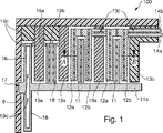
図2に表わされた基板10上には、加速センサー100のセンサー素子12が構造化されている。これは、ばね体16(これは、分かり易くするために、図1には単に唯一のばね体16が表わされている)に配置された可動中心物体または震動物体11aからなり、これらの物体は、ばね体に対して垂直に設けられた電極フィンガまたは電極11を有する。中心物体または震動物体11aは、ばね体16および固定化構造体17(これは、分かり易くするために、同様に単に1つだけが表わされている)上で基板10に丁番付けにされており、したがって中心物体11aは、この中心物体上に作用する加速度のために、本質的に電極フィンガ11に対して垂直方向である1つの方向に転向されうる。それによって、中心物体11aの位置は、固定された電極フィンガまたは対向電極12aおよび12bに対して変化される。この位置の変化は、公知方法で対向電極12aおよび12bでの電気的接触により評価され、ならびに外向きに案内されている導電路14aおよび14bにより評価される。3個の電極12a、11、12bは、それぞれ所謂インパルス列装置中に配置されており、この場合この装置は、側方向に隣接した2個の分離構造体または支持構造体13aの間に設けられた、それぞれ容量素子を形成する。可動電極フィンガ11の転向は、停止アーム18(これは、分かり易くするために、図1に単に1つだけが表わされている)および停止ノブ19a(x軸での転向)および19b(y軸での転向)によって制限されている。ばね体16の範囲内には、有利にばね体16の半分を阻止する停止ノブ19cおよび19dが設けられている。
【0007】
また、本発明によれば、2個以上の容量素子が2個の隣接した支持構造体13aの間に設けられていてよいことは、自明のことである。更に、中心物体11a中の切欠を通して係合されかつ基板10と結合されている支持構造体は、選択的または補充的に設けられていてよい(図示されていない)。
【0008】
支持構造体13aは、有利には完全にシリコン中に形成されており、それによって、以下図3〜12につき記載された、本発明による構造素子を製造するための本発明による方法の場合のように、犠牲層のエッチング、即ち下部の犠牲層31および上部の犠牲層52のエッチングまたは除去の際に(図10および11参照)、支持構造体13aの下部でのエッチングは、有効に回避される。導電路14aおよび14bは、支持構造体13cを通って支持構造体13a中に延在し、この場合犠牲層は、導電路を支持構造体から絶縁する。加速センサー100の接点15に対向した支持構造体13bは、導電路14aと14bまたは対向電極12aと12bの外部接触のために同様に14aと14bのための電気的に絶縁されたスルーホールを有する。
【0009】
次に、図3〜図12につき詳細に記載された連続プロセスを用いた場合には、なかんずく支持するキャップ層20は、図1に部分的断面図で表された加速センサー100上に製造されている。キャップ層20は、結合部23により、空隙22が容量素子上に固定されるように支持構造体13a上に貯蔵される。空隙22は、有利に約20μm〜200μmの範囲内の間にある固定幅を有する。キャップ層20は、加速センサー100の製造法において使用される犠牲層31および52を選択的に構造素子構造体に関連してエッチングしうるかまたは除去しうるために、分かり易いように単に2つの参照符号21で示されている穿孔21を備えている。犠牲層のエッチング後に、構造素子または加速センサー100の穿孔21は、密閉層24によって気密になるように閉鎖される。加速センサーまたはジャイロメーターのためには、真空またはガスを定義された圧力で空隙22内で機能素子、例えば可動電極フィンガ11の運動の定義された緩衝性を調節するために封入することができる。更に、別の構造素子、例えばアクチュエーターの場合には、適当な粘度を有する絶縁性液体、例えば油状液体の使用も考えることができる。
【0010】
図3は、深部構造化後および犠牲層エッチング前であるような、例示的に図2中でAで示された、加速センサーの部分のための加速センサー100のセンサー構造体の原理的な構造を示す。支持体10上には、例えば1つ以上のSiO2層からなることができる犠牲層31が付着されている。更に、犠牲層31上には、センサー素子または機能素子12が付着されており、この素子は、薄手のポリ−Si−種晶層12′(出発ポリ)上に付着されたエピポリシリコン、即ちエピタキシャルにより製造された多結晶性シリコンからなることができる。Si深部構造化法(トレンチエッチング)において、加速センサー100のセンサー素子12、例えば固定されている電極フィンガ12aおよび12bならびに可動中心物体11aに対して垂直に配置された電極フィンガ11が製造される。犠牲層のエッチングの前に、この機能素子は、犠牲層31上に堅固に固定されている。平面12の付着および構造化の場合には、犠牲層31の前構造化によって、基板10に対する固定部、支持構造体13a、を製造することができる。
【0011】
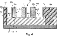
図4に示されているように、CVD法を用いて約10nm〜1μmの薄手の第1の保護層41は、センサー素子12の全体の上に付着される。それによって、第1の保護層41の範囲41aおよび41bの範囲内で、所謂電気機械的機能平面上でのセンサー素子12の完全な被覆を生じる。保護層41の範囲41cで下部の犠牲層31は被覆されている。本発明によれば、保護層41がこの保護層41とは異なる材料からなる、電気化学的機能平面上でのセンサー素子12、例えば殊に可動電極フィンガ11および対向電極12aおよび12b、ならびに加速センサー100の別の構成成分、例えば支持構造体13aを気密に被覆していることに注目することができる。保護層41は、有利にSiO2からなる。更に、下部の犠牲層31は、例えばこの実施例に記載されているようなSiO2からなることができる。
【0012】
犠牲層31は、選択的な実施態様の場合に他の保護層中に封入されていてよく(図示されていない)、さらに好ましくは多結晶性シリコンから製造されている。
【0013】
保護層41を製造するのに好ましい付着法は、CVD法、例えばPECVD(プラズマ強化CVD)またはLPCVD(低圧CVD)であり、この場合には、電気化学的機能平面上でのセンサー素子12の構成成分の側面、範囲41b、のできるだけ良好な被覆に注目することができる。
【0014】
図5に示されているように、もう1つの処理工程において、保護層41上には、薄手の出発−ポリ−Si層51、即ち種晶層または核形成層の機能を有する多結晶性シリコン層が付着される。大きなアスペクト比、即ちセンサー素子12の領域51c内での間隙の高さと間隙幅との比に基づいて、出発−ポリ−Si層51は、なかんずくセンサー素子12上での上側領域51a内に付着し、センサー素子12の側壁51bでの付着は、この側壁の上側領域内でのみ行なわれることが生じる。保護層41の領域41cの上方でのセンサー素子12の脚部の領域51cは、センサー素子12の電極間または支持構造体間での間隙幅がよりいっそう大きい場合にのみ出発−ポリ−Si層51で被覆される。出発−ポリ−Si層51上には、エピタキシー法またはLPCVD法で多結晶性シリコン層、所謂充填−エピポリ−Si層、犠牲層52、が施こされており、この場合出発−ポリ−Si層51は、上部の犠牲層52に合併されている。「エピ」は、「エピタキシャル」を意味し、「ポリ」は、「多結晶性」を表わす。上部の犠牲層52は、付着の際に既に燐がドープされていてよいが;しかし、好ましくは、ドープされないで付着される。上部の犠牲層52の層厚は、センサー素子12が完全に上部の犠牲層によって被覆されるように選択されている。これは、典型的には、約5〜30μmの層厚の場合である。
【0015】
このような層厚の充填−エピポリ−Si層または犠牲層は、一般に著しい荒さを有する。その上、センサー素子12の微細構成部(Topographie)は、上部の犠牲層52中に打ち込まれている。従って、センサー素子12の微細構成部および上部の犠牲層52の粗面は、もう1つの処理工程で平坦化される。これは、化学機械研磨(CMP)によって行なわれ、この場合には、上部の犠牲層52は、平面53になるまで薄くされる。平面53は、センサー素子12の上方に存在する。センサー素子12の上方の高さhは、ほぼ1〜30μmの間にあり;好ましい高さは、約4〜6μmである。
【0016】
平坦化後、上部の犠牲層52の構造化は、公知のSiエッチング法で、例えば図6に明示されているように行なわれる。この場合、上部の犠牲層52は、その中に可動センサー素子、例えばばね体16、可動電極フィンガ11、固定電極フィンガまたは対向電極12aおよび12bならびに中心物体または震動物体11aが配置されている領域内に放置されている。上部の犠牲層52は、分離構造体または支持構造体13aの上方で酸化シリコン保護層41に到るまで下向きに距離を有している。
【0017】
図7に相応して、構造化された上部の犠牲層52上には、第2の保護層71が施こされている。この保護層71は、有利に第1の保護層41と同じ材料、殊にSiO2からなる。保護層71は、支持構造体13a上で領域72内で公知方法により距離を有している。本発明によれば、上部の犠牲層52は、加速センサー100の全体上で保護層41および71によって気密になるように包囲されており、センサー素子12と上部の犠牲層52との間が結合されていないことが保証されていなければならない。センサー素子12と上部の犠牲層52は、有利に同じ材料からなる。更に、保護層41および71が固定領域上または支持構造体13a上で互いの中へ移行しているかまたは互いに気密になるように存在していることは、好ましい。
【0018】
図8に示されているように、保護層71上および離れた領域72上には、全面的に約300nm〜2μmの好ましい層厚を有する他の出発−ポリ−Si層または核形成層または種晶層81が施こされている。この出発−ポリ−Si層81上には、他のポリシリコン層82がエピタキシャル法またはLPCVD法で付着される。層厚は、有利に約2〜50μmである。次に、ポリシリコン層82は、平面83に到るまで薄くされ、平坦化される。第2の保護層71と平面83との間の残りの厚さkは、好ましくは約2〜50μmである。ポリシリコン層82は、付着の際にドープされてもよいし、次の処理工程でドープされてもよい。
【0019】
即ち、本発明の本質的な視点は、機能層または機能素子を少なくとも部分的に包囲する空隙をマイクロマシーニング構造素子中に得るために、構造化されたポリ−Si−機能層、例えば可動センサー素子または他の機能素子を、例えば酸化シリコンからの有利に薄手の保護層で完全に被覆し(図4参照)、この薄手の保護層上に他の多結晶性シリコン層または充填層、上部の犠牲層、を付着させる(図5参照)ことにある。構造素子の構造体平面または機能層は、多結晶性シリコン層によって埋設されており、完全に被覆されている。
【0020】
更に、本発明の重要な視点は、上部の犠牲層を平坦化し、他の薄手の保護層で外向きに密閉することにある(図6および7参照)。上部の犠牲層を外向きに密閉する前記保護層上には、厚手のポリ−Si層が付着されており、この厚手のポリ−Si層は、支持層として構造素子またはセンサーキャップを形成している(図8参照)。
【0021】
本発明によれば、上部の犠牲層は機能層と同じ材料からなることが設けられている。本発明により使用される犠牲層は、2つの緊密な保護層によって包囲されており、したがって犠牲層は、保護層に対して選択的にエッチングされることができるかまたはエッチングによって除去されることができる。更に、保護層は、下部の犠牲層のエッチングの際に除去される。この点において、充填層または上部の犠牲層の本発明による使用により、機能層中の大きな間隙幅が充填されていてもよいことは、好ましく、例えばこの機能層の1つの層は、センサーである(図5参照)。それによって、構造素子の設計の場合またはセンサーの設計の場合には、高い自由度を達成することができ、殊にこのことは、構造素子またはセンサー中に設けられた振動構造体または可動構造体の運動の自由度を許容しうる。
【0022】
上部の犠牲層の平坦化工程により(図8参照)、微細構成部は平準化され、それによってさらに上部の犠牲層の構造化は、フォトリソグラフィーによって可能である。この種の平坦化は、充填層材料または犠牲層としてのシリコンの本発明による使用によって初めて可能となる。本発明による方法の場合には、好ましくは、等方性のシリコンエッチング工程が使用され、このシリコンエッチング工程は、上部の犠牲層または充填層の残留物を含まない迅速な除去を可能にする。
【0023】
本発明による方法のもう1つの方法は、機能層またはセンサー素子を外部接触させるための金属接点およびセンサー素子によって発信される、評価のための測定信号の他の導線を処理の終結時に初めて取り付けることができることにある。
【0024】
本発明による方法は、多数のセンサー構造素子およびアクチュエーター構造素子の製造のために表面マイクロマシーニング技術において使用されることができる。同様に、センサー構造体またはアクチュエーター構造体をこれらの構造体から発信される測定信号を評価するための評価回路と一緒に唯一のチップ上に組み込むことができる。
【0025】
ポリシリコン層82の平坦化およびドーピングの後に、このポリシリコン層には、塗料マスクまたは酸化物マスク83が設けられ、このポリシリコン層は、公知のシリコン深部エッチング法で構造化される(図9参照)。この場合、ポリシリコン層82によって穿孔84は、上部の犠牲層52に接近するように導かれ、この上部の犠牲層は、犠牲層82の深部構造化の際に最初に第2の保護層71上で終わる。キャップ層20または閉鎖層24を堅固に結合させるための支持構造体13aの領域は、穿孔の際に節約される。深部構造化の場合、十分に厚手の側壁不動態化部85が付着され、この場合には、有利に弗素含有のポリマー化合物が重要である。側壁不動態化部85は、ポリシリコン層82が後のシリコンエッチング工程の際に攻撃されないことを保証する1つの層である。側壁不動態化部のためのポリマーと共に、側壁の保護のためには、保護層41および71と共に、例えば酸化シリコンからなる他の薄手の保護層を付着させることができる。
【0026】
図10の記載と同様に、保護層71は、直ぐ次の工程で穿孔または溝84内で通常のエッチング法を用いて除去される。それによって、直ぐ次のエッチングのために上部の犠牲層52への直接の入口が得られる。
【0027】
図11は、キャップ層20を得るための中心工程を示し、この場合、上部の犠牲層52は、保護層41および71に対して選択的にエッチングされている。このために、好ましくは等方的なエッチング法が使用され、例えばこの方法の場合には、XeF2、ClF3、ClF5またはプラズマ活性化されたNF3、Ar/F2もしくはSF6のエッチング媒体が使用される。保護層41および71と比較して上部の犠牲層52の選択的なエッチングの場合には、上部の犠牲層52のエッチングは、保護層41および71に対する境界面で停止される。キャップ層20を形成するポリシリコン層82内での穿孔84の側壁のエッチングは、施こされた側壁不動態化部85によって抑制される。処理の終結時に、上部の犠牲層52は、完全にエッチングされているかまたは溶解されている。この上部の犠牲層は、センサー素子12上に空隙22を生じ、このセンサー素子上には、安定な支持ポリシリコン層82またはキャップ層20(殊に図2参照)が懸吊されている。図12に相応して、上部の犠牲層52のエッチング後に、補助層である保護層41および71ならびに下部の犠牲層31は、センサー素子12およびキャップ層20(図2参照)を形成するポリシリコン層82に対して選択的にエッチングされる。このためには、例えば蒸気状HF/H2O混合物の使用に基づく、SiO2層をエッチングするための方法を使用することができる。この方法の場合には、ガス状HFおよびH2Oは、キャップ層20の穿孔84を突き進み、保護層41および71に到達し、ならびにこれらの保護層のエッチング後に下部の犠牲層31に到達する。このエッチング工程の後、保護層または酸化物層41および71ならびに下部の犠牲層31は除去されており、センサー素子12の全ての可動構造体、例えば中心物体11a、ばね体16、停止アーム18および可動電極フィンガ11は、基板10から自由に離れている(殊に、図1および2参照)。ガス状雰囲気中での前記エッチング工程に続いて、ポリシリコン層82またはキャップ層20の穿孔84は、被覆層120で封鎖される。被覆層120は、有利に約1〜120μmの厚さであり、例えば有利にPECVD法で付着されている絶縁体、有利にSiO2からなる。被覆層120を付着させる場合には、好ましくは同時にプロセスガスは、空隙22内に封入され、それによって封入されたプロセスガスの圧力および/または種類に依存して、本発明による加速センサーのセンサー素子12の可動構成成分の動的緩衝性を調節することができる。本発明による加速センサー100内に設けられた可動構成成分の運動を緩衝するガスの封入は、勿論、付着工程とは無関係の他の処理工程の場合にも行なうことができる。
【0028】
被覆層120の付着の後、金属導体路14aおよび14bならびに接点15は、公知方法で製造される。
【0029】
本発明の選択的な実施態様(図示されていない)の場合には、下部の犠牲層31および上部の犠牲層52は、それぞれポリシリコンから形成されており、これに対して、下部の犠牲層31は、図3〜12に示された方法の場合にSiO2から形成されている。選択的な実施態様の場合には、基板10上に下部の保護層(図示されていない)が付着される。これには、ポリシリコン緩衝層の付着が続き、次に、このポリシリコン緩衝層上には、上部の保護層(図示されていない)が付着され、したがって下部の犠牲層31は、下部の保護層および上部の保護層によって完全に包囲されている。下部の保護層は、基板10のエッチング攻撃からの保護に使用され、上部の保護層は、下部の犠牲層の選択的なエッチングまたは除去の際にエッチング攻撃からセンサー素子12または機能層13a、13b、13cを保護する。2つの緩衝層のための保護層は、有利に酸化シリコンから形成されており、したがって同じ材料の2つの緩衝層は、唯一かまたは多数のエッチング工程で除去されることができる。
【0030】
図に示された加速センサーのように、本発明による方法で製造しうる構造素子の平坦性に基づき、センサー/アクチュエーター構造体および組み込まれた評価開閉回路を唯一のチップまたは構造素子上に組み込むこと(図示されていない)は、簡単に可能である。このために、最初に上部の犠牲層およびキャップ層を有するセンサー素子の平面は、記載された方法で製造されなければならない。このようなチップまたは構造素子における電子回路の故障を回避させるために、キャップ層の穿孔、上部の犠牲層のエッチング、保護層の除去および被覆層での空隙の密閉ならびにこのようなチップまたは構造素子の開閉回路の製造後の接点の電気的接続を実施することは、有利である。この処理工程の場合には、なお低い温度のみが発生し、したがって例えばトランジスタを有することができる開閉回路は、損なわれることがない。
【0031】
本発明の前記の説明により、本発明が本発明による加速センサーまたはこの加速センサーを製造するための本発明による方法に制限されるだけでなく、むしろ空隙、殊に気密になるように密閉された空隙を有する多数のマイクロマシーニング構造素子の製造を可能にすることが明らかになる。
【0032】
これは、殊に空隙内にマイクロマシーニング技術の全範囲からの可動要素、例えばセンサー素子またはマイクロポンプの構成成分等が設けられている場合に云えることである。
【図面の簡単な説明】
【図1】 機能素子またはセンサー素子の範囲内の加速センサーを示す断面図。
【図2】 付加的に接点が収容されている、図1中の切断線A−Bに沿っての図1に表わされた範囲を示す断面図。
【図3】 図1および図2に表わされた本発明による加速センサーを製造するための本発明による1つの方法を示す略図。
【図4】 図1および図2に表わされた本発明による加速センサーを製造するための本発明による1つの方法を示す略図。
【図5】 図1および図2に表わされた本発明による加速センサーを製造するための本発明による1つの方法を示す略図。
【図6】 図1および図2に表わされた本発明による加速センサーを製造するための本発明による1つの方法を示す略図。
【図7】 図1および図2に表わされた本発明による加速センサーを製造するための本発明による1つの方法を示す略図。
【図8】 図1および図2に表わされた本発明による加速センサーを製造するための本発明による1つの方法を示す略図。
【図9】 図1および図2に表わされた本発明による加速センサーを製造するための本発明による1つの方法を示す略図。
【図10】 図1および図2に表わされた本発明による加速センサーを製造するための本発明による1つの方法を示す略図。
【図11】 図1および図2に表わされた本発明による加速センサーを製造するための本発明による1つの方法を示す略図。
【図12】 図1および図2に表わされた本発明による加速センサーを製造するための本発明による1つの方法を示す略図。
【符号の説明】
10 基板、 11 可動電極フィンガ、11a 中心物体、 12 センサー素子、 12a、12b 対向電極、 13a 側方向に隣接した2個の支持構造体、 13b 支持構造体、 13c 支持構造体、 14a、14b 導電路、 16 ばね体、 17 固定化構造体、 18 停止アーム、 19a 停止ノブ(x軸での転向)、 19b 停止ノブ(y軸での転向)、 19c ばね体16の半分を阻止する停止ノブ、 19d ばね体16の半分を阻止する停止ノブ、 20、82 キャップ層、 21 穿孔、 22 空隙、 23 結合部、 24 密閉層、 31 第2の犠牲層、 41 第1の保護層、41a、41b、41c 第1の保護層41の範囲、 51c センサー素子12の脚部の領域、 52 第1の犠牲層、 71 第2の保護層、 81 核形成層、 82 ポリシリコン層、 100 加速センサー[0001]
Technical level
The invention starts from a method of manufacturing a micromachining structure element and a micromachining structure element manufactured by this method as described in the superordinate concept of the independent claim. German patent application DE 195 37 814 A1 relates to the structure of a sensor layer system and a method for hermetically capping a sensor in surface micromachining technology.
[0002]
Advantages of the invention
On the other hand, the method according to the invention with the features of the independent claims has the advantage that, in particular, a hermetically sealed structural element can be produced inexpensively. By means of the dependent claims, other preferred formations and improvements of the method and the structural element are possible by the description of the independent claims.
[0003]
The structural elements according to the present invention show a clear reduction in the surface area required for capping compared to known structural elements, which involves significant cost savings for the surface area savings. In the case of a structural element according to the invention, for example a sensor, the freedom of movement for the movable structure provided in the structural element is maintained as it is, and in practice about 2 μm is used for the freedom of movement. Even if it is necessary to achieve greater lateral amplitude, it remains intact. This is the case, for example, when the movable structure or the functional element is a rotary vibrating body. On the other hand, the maximum deflection of the movable structure can be limited to an amplitude of about 2 to 20 μm in the direction perpendicular to the sensor, for example in the case of a sensor, which is particularly the case for known structural elements. This clearly increases the drop strength of the structural element according to the invention. The movable structure or the sensor structure is surrounded by a gap so as to be airtight and / or watertight in the structural element according to the invention, and thus, for example, due to the gas pressure of the gas enclosed in the gap, A defined long-term stable buffering of the movement of the sensor structure can be adjusted in the air gap. The capping according to the invention exhibits a high machining stability, so that the structural element according to the invention is subjected to hydrostatic pressure, such as occurs in the plastic casing during the packing process of the micromachined structural element, for example during so-called molding pressure. Endure without hardship. Finally, the structural element according to the invention or the sensor according to the invention exhibits a low topographie, which allows the use of so-called flip-chip technology, for example when mounting the structural element.
[0004]
In the case of the method according to the invention, preferably the known use of oxide layers having a thickness of more than about 2 μm is omitted. Rather, a thick layer, advantageously formed sufficiently in polycrystalline silicon, is used, whereby the mechanical stress can be clearly reduced based on different coefficients of thermal expansion. This results in a significantly improved flatness of the substrate. The method according to the invention allows the problem-free use of the optical lithography process. This is because topography exceeding 6 μm is advantageously avoided. Finally, one or more isotropic etching methods, preferably removing one or more sacrificial layers (filling material) in the micromachined structural element, for example for the manufacture of voids with movable structures used. Such an isotropic (silicon) etching method is a method in which the etching medium XeF2, ClF3, ClF5 or plasma activated NF3, Ar / F2 or SF6 is used. In this case, the removal takes place without the danger of the structures to be exposed at the high grinding speed of the filling material to be removed, compared with the known methods.
[0005]
The invention will now be described in detail with reference to the drawings, which are deviated from scale, if necessary, wherein the same reference numerals denote the same or similarly acting layers or parts.
[0006]
The
[0007]
In addition, according to the present invention, it is obvious that two or more capacitive elements may be provided between two
[0008]
The
[0009]
Next, when using the continuous process described in detail with reference to FIGS. 3-12, the supporting
[0010]
FIG. 3 illustrates the basic structure of the sensor structure of the
[0011]
As shown in FIG. 4, a thin first
[0012]
The
[0013]
A preferred deposition method for producing the
[0014]
As shown in FIG. 5, in another processing step, on the
[0015]
Such a fill-epipoly-Si layer or sacrificial layer of layer thickness generally has a significant roughness. In addition, the topography of the
[0016]
After planarization, the upper
[0017]
Corresponding to FIG. 7, a second
[0018]
As shown in FIG. 8, other starting-poly-Si layers or nucleation layers or seeds having a preferred layer thickness of about 300 nm to 2 μm over the entire surface on the
[0019]
That is, an essential aspect of the present invention is that a structured poly-Si-functional layer, such as a movable sensor, is obtained in order to obtain a void in the micromachined structural element that at least partially surrounds the functional layer or functional element. The element or other functional element is completely covered, for example with a thin protective layer, preferably from silicon oxide (see FIG. 4), on top of this thin protective layer another polycrystalline silicon layer or filling layer, on top A sacrificial layer is deposited (see FIG. 5). The structure plane or functional layer of the structural element is buried by a polycrystalline silicon layer and is completely covered.
[0020]
In addition, an important aspect of the present invention is to planarize the upper sacrificial layer and seal it outward with another thin protective layer (see FIGS. 6 and 7). A thick poly-Si layer is deposited on the protective layer that seals the upper sacrificial layer outward, and this thick poly-Si layer forms a structural element or sensor cap as a support layer. (See FIG. 8).
[0021]
According to the invention, it is provided that the upper sacrificial layer is made of the same material as the functional layer. The sacrificial layer used according to the invention is surrounded by two tight protective layers, so that the sacrificial layer can be selectively etched or removed by etching with respect to the protective layer. it can. Furthermore, the protective layer is removed during the etching of the lower sacrificial layer. In this respect, it is preferred that a large gap width in the functional layer may be filled by the use of the filling layer or the upper sacrificial layer according to the invention, for example one layer of this functional layer is a sensor (See FIG. 5). Thereby, a high degree of freedom can be achieved in the case of the design of structural elements or in the case of sensor designs, in particular this means that a vibrating or movable structure provided in the structural element or sensor. The degree of freedom of movement can be tolerated.
[0022]
By the step of planarizing the upper sacrificial layer (see FIG. 8), the fine structure is leveled, and thus further structuring of the upper sacrificial layer is possible by photolithography. This kind of planarization is only possible with the use according to the invention of silicon as filling layer material or sacrificial layer. In the case of the method according to the invention, preferably an isotropic silicon etching process is used, which allows a rapid removal without the residue of the upper sacrificial layer or filling layer.
[0023]
Another method of the method according to the invention is to attach for the first time at the end of the process the metal contacts for external contact of the functional layer or sensor element and the other conductors of the measurement signal for evaluation emitted by the sensor element. There is in being able to.
[0024]
The method according to the invention can be used in surface micromachining technology for the production of a large number of sensor structural elements and actuator structural elements. Similarly, sensor structures or actuator structures can be integrated on a single chip together with an evaluation circuit for evaluating the measurement signals emitted from these structures.
[0025]
After planarization and doping of the
[0026]
As in the description of FIG. 10, the
[0027]
FIG. 11 shows a central process for obtaining the
[0028]
After deposition of the
[0029]
In an alternative embodiment (not shown) of the present invention, the lower
[0030]
Based on the flatness of the structural elements that can be produced by the method according to the invention, such as the acceleration sensor shown in the figure, the sensor / actuator structure and the built-in evaluation switching circuit are integrated on a single chip or structural element. (Not shown) is easily possible. For this purpose, the plane of the sensor element with the upper sacrificial layer and cap layer first must be manufactured in the manner described. In order to avoid failure of the electronic circuit in such a chip or structural element, perforation of the cap layer, etching of the upper sacrificial layer, removal of the protective layer and sealing of the air gap in the covering layer and such chip or structural element It is advantageous to carry out the electrical connection of the contacts after the manufacture of the switch circuit. In the case of this processing step, only a low temperature still occurs, so that the switching circuit that can have, for example, a transistor is not impaired.
[0031]
By the above description of the invention, the invention is not limited to the acceleration sensor according to the invention or the method according to the invention for manufacturing this acceleration sensor, but rather is sealed to be airtight, in particular airtight. It becomes clear that a large number of micromachined structural elements with voids can be produced.
[0032]
This is especially true if the gap is provided with movable elements from the full range of micromachining technology, such as sensor elements or components of a micropump.
[Brief description of the drawings]
FIG. 1 is a cross-sectional view showing an acceleration sensor within a range of a functional element or a sensor element.
2 is a cross-sectional view showing the range represented in FIG. 1 along the section line AB in FIG. 1, additionally containing contacts.
FIG. 3 is a schematic diagram illustrating one method according to the present invention for manufacturing the acceleration sensor according to the present invention represented in FIGS. 1 and 2;
4 is a schematic diagram illustrating one method according to the present invention for manufacturing the acceleration sensor according to the present invention represented in FIGS. 1 and 2. FIG.
FIG. 5 is a schematic diagram illustrating one method according to the present invention for manufacturing the acceleration sensor according to the present invention represented in FIGS. 1 and 2;
6 is a schematic diagram illustrating one method according to the present invention for manufacturing the acceleration sensor according to the present invention represented in FIGS. 1 and 2. FIG.
7 is a schematic diagram illustrating one method according to the present invention for manufacturing the acceleration sensor according to the present invention represented in FIGS. 1 and 2. FIG.
FIG. 8 is a schematic diagram illustrating one method according to the present invention for manufacturing the acceleration sensor according to the present invention represented in FIGS. 1 and 2;
9 is a schematic diagram illustrating one method according to the present invention for manufacturing the acceleration sensor according to the present invention represented in FIGS. 1 and 2. FIG.
10 is a schematic diagram illustrating one method according to the present invention for manufacturing the acceleration sensor according to the present invention represented in FIGS. 1 and 2. FIG.
11 is a schematic diagram showing one method according to the present invention for manufacturing the acceleration sensor according to the present invention represented in FIGS. 1 and 2. FIG.
12 is a schematic diagram illustrating one method according to the present invention for manufacturing the acceleration sensor according to the present invention represented in FIGS. 1 and 2. FIG.
[Explanation of symbols]
DESCRIPTION OF
Claims (7)
その際、機能素子(12)に、少なくとも、次に1つ以上のエッチング段階で形成される空隙(22)の空間を一時的に少なくとも部分的に占める第1の犠牲層(52)と直接的または間接的に境を接している範囲内で第1の保護層(41)を備えさせ、その際に第1の保護層(41)の材料は、第1の犠牲層(52)をエッチングする少なくとも1つのエッチング媒体により、第1の保護層(41)が十分にエッチングされないかまたは単に第1の犠牲層(52)に関して減少したエッチング速度でエッチングされるように選択され、その際、機能素子(12)とは反対側の第1の犠牲層(52)の少なくとも1つの面上に第1の犠牲層(52)の第2の保護層(71)を設け、この場合第2の保護層(71)の材料は、第1の犠牲層(52)をエッチングする少なくとも1つのエッチング媒体により、第2の保護層(71)が十分にエッチングされないかまたは単に第1の犠牲層(52)に関して減少したエッチング速度でエッチングされるように選択され、その際、第1の犠牲層(52)とは反対側の第2の保護層(71)の面上に、空隙(22)を少なくとも部分的に包囲するキャップ層(20;82)を設け、その際、機能素子(12)は、直接的または間接的に第2の犠牲層(31)と境を接し、この第2の犠牲層(31)は、第2の犠牲層(31)をエッチングする少なくとも1つのエッチング媒体により、機能素子(12)が十分にエッチングされないかまたは単に第2の犠牲層(31)に関して減少したエッチング速度でエッチングされるように選択され、この場合、機能素子(12)ならびに第1の犠牲層(52)および/または第2の犠牲層(31)には、同じ材料が選択される、マイクロマシーニング構造素子(100)の製造法。A method of manufacturing a micromachined structural element (100) having at least one void (22) and a functional element (12 ) provided at least partially in the void (22) , comprising:
During its, to the functional element (12), at least, then space temporarily at least a first sacrificial layer partially occupied (52) the direct air gap (22) that will be formed by one or more etching steps or indirectly by comprising a first protective layer within the range that bordering (41), the material of the first protective layer (41) at that time, the first sacrificial layer (52) the single d etching medium even without least etched, to be etched in the first protective layer (41) has not been sufficiently etched or simply etch rate decreased regarding the first sacrificial layer (52) is selected, this time, the second protective layer of the functional element the first sacrificial layer on at least one surface of the first sacrificial layer opposite to the (12) (52) (52) (71) In this case, the material of the second protective layer (71) is the first sacrificial layer (5 The at least one etching medium etching 2) is selected such that the second protective layer (71) is not sufficiently etched or is etched at a reduced etch rate with respect to the first sacrificial layer (52); In that case, on the surface of the second protective layer (71) opposite to the first sacrificial layer (52) , a cap layer (20; 82) that at least partially surrounds the gap (22) is provided, At that time, the functional element (12) directly or indirectly contacts the second sacrificial layer (31), and the second sacrificial layer (31) etches the second sacrificial layer (31). by at least one etching medium, the functional element (12) is selected to be etched at a reduced etch rate with respect to fully or just the second sacrificial layer is not etched (31), this If, on the functional element (12) and the first sacrificial layer (52) and / or the second sacrificial layer (31), the same material is selected, preparation of micromachining the structural element (100).
その際、機能層(13a、13b、13c)に、少なくとも、次に1つ以上のエッチング段階で形成される空隙(22)の空間を一時的に少なくとも部分的に占める第1の犠牲層(52)と直接的または間接的に境を接している範囲内で第1の保護層(41)を備えさせ、その際に第1の保護層(41)の材料は、第1の犠牲層(52)をエッチングする少なくとも1つのエッチング媒体により、第1の保護層(41)が十分にエッチングされないかまたは単に第1の犠牲層(52)に関して減少したエッチング速度でエッチングされるように選択され、その際、機能層(13a、13b、13c)とは反対側の第1の犠牲層(52)の少なくとも1つの面上に第1の犠牲層(52)の第2の保護層(71)を設け、この場合第2の保護層(71)の材料は、第1の犠牲層(52)をエッチングする少なくとも1つのエッチング媒体により、第2の保護層(71)が十分にエッチングされないかまたは単に第1の犠牲層(52)に関して減少したエッチング速度でエッチングされるように選択され、その際、第1の犠牲層(52)とは反対側の第2の保護層(71)の面上に、空隙(22)を少なくとも部分的に包囲するキャップ層(20;82)を設け、その際、機能層(13a、13b、13c)は、直接的または間接的に第2の犠牲層(31)と境を接し、この第2の犠牲層(31)は、第2の犠牲層(31)をエッチングする少なくとも1つのエッチング媒体により、機能層(13a、13b、13c)が十分にエッチングされないかまたは単に第2の犠牲層(31)に関して減少したエッチング速度でエッチングされるように選択され、この場合、機能層(13a、13b、13c)ならびに第1の犠牲層(52)および/または第2の犠牲層(31)には、同じ材料が選択される、マイクロマシーニング構造素子(100)の製造法。 A method of manufacturing a micromachined structural element (100) having at least one void (22) and a functional layer (13a, 13b, 13c) provided at least partially in the void (22),
In doing so, the first sacrificial layer (52) that temporarily occupies at least partially the space (22) formed in the functional layer (13a, 13b, 13c) at least in the next one or more etching steps. The first protective layer (41) is provided within a range directly or indirectly in contact with the first protective layer (41). In this case, the material of the first protective layer (41) is the first sacrificial layer (52). The first protective layer (41) is selected not to be sufficiently etched or simply etched at a reduced etch rate with respect to the first sacrificial layer (52), In this case, the second protective layer (71) of the first sacrificial layer (52) is provided on at least one surface of the first sacrificial layer (52) opposite to the functional layer (13a, 13b, 13c). , In this case the second protective layer ( The material of 1) is reduced with respect to the first sacrificial layer (52) by the at least one etching medium that etches the first sacrificial layer (52) or the second protective layer (71) is not sufficiently etched. At a part of the surface of the second protective layer (71) opposite to the first sacrificial layer (52) at least partially. An enclosing cap layer (20; 82) is provided, wherein the functional layer (13a, 13b, 13c) directly or indirectly borders the second sacrificial layer (31) and this second sacrificial layer The layer (31) is not sufficiently etched by the at least one etching medium that etches the second sacrificial layer (31) or the functional layer (13a, 13b, 13c) is simply etched into the second sacrificial layer (31). Seki In this case, the functional layers (13a, 13b, 13c) and the first sacrificial layer (52) and / or the second sacrificial layer (31) are the same. A method of manufacturing a micromachined structural element (100), wherein the material is selected .
Applications Claiming Priority (3)
| Application Number | Priority Date | Filing Date | Title |
|---|---|---|---|
| DE10006035.8 | 2000-02-10 | ||
| DE10006035A DE10006035A1 (en) | 2000-02-10 | 2000-02-10 | Micro-mechanical component production, used as sensor element or actuator element, comprises providing functional element and/or functional layer with protective layer |
| PCT/DE2000/004673 WO2001058803A2 (en) | 2000-02-10 | 2000-12-28 | Method for producing a micromechanical component, and a component produced according to said method |
Publications (3)
| Publication Number | Publication Date |
|---|---|
| JP2003531017A JP2003531017A (en) | 2003-10-21 |
| JP2003531017A5 JP2003531017A5 (en) | 2011-09-08 |
| JP4838476B2 true JP4838476B2 (en) | 2011-12-14 |
Family
ID=7630549
Family Applications (1)
| Application Number | Title | Priority Date | Filing Date |
|---|---|---|---|
| JP2001558361A Expired - Fee Related JP4838476B2 (en) | 2000-02-10 | 2000-12-28 | Micromachining structural element manufacturing method and structural element manufactured by the method |
Country Status (5)
| Country | Link |
|---|---|
| US (1) | US6951824B2 (en) |
| EP (1) | EP1257496A2 (en) |
| JP (1) | JP4838476B2 (en) |
| DE (1) | DE10006035A1 (en) |
| WO (1) | WO2001058803A2 (en) |
Families Citing this family (54)
| Publication number | Priority date | Publication date | Assignee | Title |
|---|---|---|---|---|
| US7550794B2 (en) | 2002-09-20 | 2009-06-23 | Idc, Llc | Micromechanical systems device comprising a displaceable electrode and a charge-trapping layer |
| DE10047189C1 (en) * | 2000-09-23 | 2002-02-21 | Bosch Gmbh Robert | Seat occupant classification method for automobile passenger seat uses evaluation of seating profile provided by pressure sensor matrix |
| DE10117257A1 (en) * | 2001-04-06 | 2002-10-17 | Eads Deutschland Gmbh | Micromechanical capacitive acceleration sensor |
| KR20040105862A (en) * | 2002-04-10 | 2004-12-16 | 피셔 앤 페이켈 어플라이언스 리미티드 | A laundry appliance |
| DE10231729B4 (en) * | 2002-07-13 | 2011-08-11 | Robert Bosch GmbH, 70469 | Component with a surface micromechanical structure |
| US7781850B2 (en) * | 2002-09-20 | 2010-08-24 | Qualcomm Mems Technologies, Inc. | Controlling electromechanical behavior of structures within a microelectromechanical systems device |
| DE10246283B3 (en) * | 2002-10-02 | 2004-03-25 | Infineon Technologies Ag | Production of an electronic component used in semiconductor sensors comprises preparing a semiconductor chip on a switching substrate, applying a sacrificial part on the sensor region of the chip and further processing |
| US6939809B2 (en) * | 2002-12-30 | 2005-09-06 | Robert Bosch Gmbh | Method for release of surface micromachined structures in an epitaxial reactor |
| US20040166606A1 (en) * | 2003-02-26 | 2004-08-26 | David Forehand | Low temperature wafer-level micro-encapsulation |
| US7514283B2 (en) * | 2003-03-20 | 2009-04-07 | Robert Bosch Gmbh | Method of fabricating electromechanical device having a controlled atmosphere |
| US7075160B2 (en) | 2003-06-04 | 2006-07-11 | Robert Bosch Gmbh | Microelectromechanical systems and devices having thin film encapsulated mechanical structures |
| US6936491B2 (en) * | 2003-06-04 | 2005-08-30 | Robert Bosch Gmbh | Method of fabricating microelectromechanical systems and devices having trench isolated contacts |
| US6952041B2 (en) * | 2003-07-25 | 2005-10-04 | Robert Bosch Gmbh | Anchors for microelectromechanical systems having an SOI substrate, and method of fabricating same |
| DE10348908B4 (en) * | 2003-10-21 | 2014-03-20 | Robert Bosch Gmbh | Method for producing a microsystem with integrated circuit and micromechanical component |
| DE102004036803A1 (en) * | 2004-07-29 | 2006-03-23 | Robert Bosch Gmbh | Method for etching a layer on a substrate |
| KR101354520B1 (en) * | 2004-07-29 | 2014-01-21 | 퀄컴 엠이엠에스 테크놀로지스, 인크. | System and method for micro-electromechanical operating of an interferometric modulator |
| JP4552783B2 (en) * | 2005-07-06 | 2010-09-29 | 株式会社デンソー | Semiconductor sensor |
| JP2009503565A (en) | 2005-07-22 | 2009-01-29 | クアルコム,インコーポレイテッド | Support structure for MEMS device and method thereof |
| KR101375337B1 (en) | 2005-07-22 | 2014-03-18 | 퀄컴 엠이엠에스 테크놀로지스, 인크. | Electomechanical devices having support structures and methods of fabricating the same |
| EP2495212A3 (en) | 2005-07-22 | 2012-10-31 | QUALCOMM MEMS Technologies, Inc. | Mems devices having support structures and methods of fabricating the same |
| JP4479006B2 (en) * | 2005-07-28 | 2010-06-09 | セイコーエプソン株式会社 | Manufacturing method of semiconductor device |
| US7956428B2 (en) | 2005-08-16 | 2011-06-07 | Robert Bosch Gmbh | Microelectromechanical devices and fabrication methods |
| US7630114B2 (en) * | 2005-10-28 | 2009-12-08 | Idc, Llc | Diffusion barrier layer for MEMS devices |
| US7795061B2 (en) | 2005-12-29 | 2010-09-14 | Qualcomm Mems Technologies, Inc. | Method of creating MEMS device cavities by a non-etching process |
| US7382515B2 (en) | 2006-01-18 | 2008-06-03 | Qualcomm Mems Technologies, Inc. | Silicon-rich silicon nitrides as etch stops in MEMS manufacture |
| US20070170528A1 (en) | 2006-01-20 | 2007-07-26 | Aaron Partridge | Wafer encapsulated microelectromechanical structure and method of manufacturing same |
| US7450295B2 (en) | 2006-03-02 | 2008-11-11 | Qualcomm Mems Technologies, Inc. | Methods for producing MEMS with protective coatings using multi-component sacrificial layers |
| DE102006024668A1 (en) | 2006-05-26 | 2007-11-29 | Robert Bosch Gmbh | Micromechanical component e.g. sensor, for e.g. hearing aid`s microphone, has counter unit with passage hole in rear volume formed by hollow space below unit, where hollow space contacts upper side of membrane below counter unit via opening |
| DE102006033176B4 (en) | 2006-07-18 | 2023-05-25 | Robert Bosch Gmbh | Micromechanical component with a stop element |
| DE102006049259A1 (en) | 2006-10-19 | 2008-04-30 | Robert Bosch Gmbh | Method for producing a micromechanical component with a thin-film capping |
| DE102006052630A1 (en) * | 2006-10-19 | 2008-04-24 | Robert Bosch Gmbh | Micromechanical component with monolithic integrated circuit and method for producing a component |
| US20080119003A1 (en) * | 2006-11-17 | 2008-05-22 | Charles Grosjean | Substrate contact for a MEMS device |
| US7733552B2 (en) | 2007-03-21 | 2010-06-08 | Qualcomm Mems Technologies, Inc | MEMS cavity-coating layers and methods |
| US7719752B2 (en) | 2007-05-11 | 2010-05-18 | Qualcomm Mems Technologies, Inc. | MEMS structures, methods of fabricating MEMS components on separate substrates and assembly of same |
| DE102007025880A1 (en) | 2007-06-01 | 2008-12-04 | Robert Bosch Gmbh | Micromechanical component and method for producing a micromechanical component with a thin-film cap |
| US8068268B2 (en) | 2007-07-03 | 2011-11-29 | Qualcomm Mems Technologies, Inc. | MEMS devices having improved uniformity and methods for making them |
| EP2235742B1 (en) * | 2007-12-21 | 2020-02-12 | Solvay Fluor GmbH | Process for the production of microelectromechanical systems |
| US7851239B2 (en) * | 2008-06-05 | 2010-12-14 | Qualcomm Mems Technologies, Inc. | Low temperature amorphous silicon sacrificial layer for controlled adhesion in MEMS devices |
| CN102196989A (en) * | 2008-10-29 | 2011-09-21 | Nxp股份有限公司 | An integrated component and a method of manufacturing an integrated component |
| DE102009027898B4 (en) * | 2009-07-21 | 2019-09-05 | Robert Bosch Gmbh | Manufacturing method for a micromechanical component |
| EP2365521B1 (en) * | 2010-01-22 | 2018-12-26 | IMEC vzw | Thin film wafer level package |
| US8384183B2 (en) * | 2010-02-19 | 2013-02-26 | Allegro Microsystems, Inc. | Integrated hall effect element having a germanium hall plate |
| CN101913552B (en) * | 2010-08-02 | 2012-02-15 | 清华大学 | Method for preparing suspension micro-sensitive structure based on aluminum sacrificial layer process |
| JP5624866B2 (en) * | 2010-12-06 | 2014-11-12 | ローム株式会社 | Manufacturing method of MEMS sensor |
| US8659816B2 (en) | 2011-04-25 | 2014-02-25 | Qualcomm Mems Technologies, Inc. | Mechanical layer and methods of making the same |
| US8648432B2 (en) * | 2011-11-28 | 2014-02-11 | Texas Instruments Deutschland Gmbh | Fully embedded micromechanical device, system on chip and method for manufacturing the same |
| US9041213B2 (en) * | 2013-03-14 | 2015-05-26 | Freescale Semiconductor Inc. | Microelectromechanical system devices having through substrate vias and methods for the fabrication thereof |
| JP6400693B2 (en) | 2013-06-27 | 2018-10-03 | ソイテックSoitec | Method for fabricating a semiconductor structure including a cavity filled with a sacrificial material |
| DE102014112672B4 (en) * | 2014-09-03 | 2018-05-09 | Snaptrack, Inc. | Cover for a component and method for producing a cover for a component |
| US9738516B2 (en) * | 2015-04-29 | 2017-08-22 | Taiwan Semiconductor Manufacturing Co., Ltd. | Structure to reduce backside silicon damage |
| US10192850B1 (en) | 2016-09-19 | 2019-01-29 | Sitime Corporation | Bonding process with inhibited oxide formation |
| CN108538835B (en) * | 2018-05-16 | 2024-02-06 | 长鑫存储技术有限公司 | Capacitor array structure and preparation method thereof |
| CN112661105B (en) * | 2020-12-29 | 2023-08-29 | 无锡微视传感科技有限公司 | Manufacturing method of MEMS (micro-electromechanical systems) high-low comb tooth structure based on comb tooth local oxidation |
| EP4361345A1 (en) | 2022-10-27 | 2024-05-01 | Toscotec SpA | Shoe press |
Citations (6)
| Publication number | Priority date | Publication date | Assignee | Title |
|---|---|---|---|---|
| JPS6055655A (en) * | 1983-09-07 | 1985-03-30 | Nissan Motor Co Ltd | Semiconductor device having beam structure |
| JPH05332852A (en) * | 1990-04-11 | 1993-12-17 | Wisconsin Alumni Res Found | Polycrystal resonance beam converter and its manufacturing method |
| US5285131A (en) * | 1990-12-03 | 1994-02-08 | University Of California - Berkeley | Vacuum-sealed silicon incandescent light |
| JPH06123628A (en) * | 1992-10-12 | 1994-05-06 | Nippondenso Co Ltd | Semiconductor dynamic sensor and production thereof |
| US5846849A (en) * | 1993-02-04 | 1998-12-08 | Cornell Research Foundation, Inc. | Microstructure and single mask, single-crystal process for fabrication thereof |
| JPH11150278A (en) * | 1997-07-10 | 1999-06-02 | St Microelectron Srl | Integrated sensor and manufacture thereof |
Family Cites Families (3)
| Publication number | Priority date | Publication date | Assignee | Title |
|---|---|---|---|---|
| US5461916A (en) * | 1992-08-21 | 1995-10-31 | Nippondenso Co., Ltd. | Mechanical force sensing semiconductor device |
| DE19537814B4 (en) | 1995-10-11 | 2009-11-19 | Robert Bosch Gmbh | Sensor and method for producing a sensor |
| US5992233A (en) * | 1996-05-31 | 1999-11-30 | The Regents Of The University Of California | Micromachined Z-axis vibratory rate gyroscope |
-
2000
- 2000-02-10 DE DE10006035A patent/DE10006035A1/en not_active Ceased
- 2000-12-28 US US10/203,729 patent/US6951824B2/en not_active Expired - Fee Related
- 2000-12-28 EP EP00990587A patent/EP1257496A2/en not_active Withdrawn
- 2000-12-28 JP JP2001558361A patent/JP4838476B2/en not_active Expired - Fee Related
- 2000-12-28 WO PCT/DE2000/004673 patent/WO2001058803A2/en active Application Filing
Patent Citations (6)
| Publication number | Priority date | Publication date | Assignee | Title |
|---|---|---|---|---|
| JPS6055655A (en) * | 1983-09-07 | 1985-03-30 | Nissan Motor Co Ltd | Semiconductor device having beam structure |
| JPH05332852A (en) * | 1990-04-11 | 1993-12-17 | Wisconsin Alumni Res Found | Polycrystal resonance beam converter and its manufacturing method |
| US5285131A (en) * | 1990-12-03 | 1994-02-08 | University Of California - Berkeley | Vacuum-sealed silicon incandescent light |
| JPH06123628A (en) * | 1992-10-12 | 1994-05-06 | Nippondenso Co Ltd | Semiconductor dynamic sensor and production thereof |
| US5846849A (en) * | 1993-02-04 | 1998-12-08 | Cornell Research Foundation, Inc. | Microstructure and single mask, single-crystal process for fabrication thereof |
| JPH11150278A (en) * | 1997-07-10 | 1999-06-02 | St Microelectron Srl | Integrated sensor and manufacture thereof |
Also Published As
| Publication number | Publication date |
|---|---|
| US20030141561A1 (en) | 2003-07-31 |
| US6951824B2 (en) | 2005-10-04 |
| DE10006035A1 (en) | 2001-08-16 |
| WO2001058803A2 (en) | 2001-08-16 |
| WO2001058803A3 (en) | 2002-03-14 |
| EP1257496A2 (en) | 2002-11-20 |
| JP2003531017A (en) | 2003-10-21 |
Similar Documents
| Publication | Publication Date | Title |
|---|---|---|
| JP4838476B2 (en) | Micromachining structural element manufacturing method and structural element manufactured by the method | |
| US7115436B2 (en) | Integrated getter area for wafer level encapsulated microelectromechanical systems | |
| JP5602761B2 (en) | Micro-electromechanical system device having separated microstructure and manufacturing method thereof | |
| JP4603740B2 (en) | Precision mechanical structural element and manufacturing method thereof | |
| US6952041B2 (en) | Anchors for microelectromechanical systems having an SOI substrate, and method of fabricating same | |
| US7671515B2 (en) | Microelectromechanical devices and fabrication methods | |
| JP5090603B2 (en) | Micromechanical structural element and corresponding manufacturing method | |
| US20070202628A1 (en) | Manufacturing process for integrated piezo elements | |
| US9988260B2 (en) | Rough MEMS surface | |
| WO2015020881A1 (en) | Inertial and pressure sensors on single chip | |
| US9034764B2 (en) | Method of forming wide trenches using a sacrificial silicon slab | |
| EP3507238A1 (en) | Mems structure with graphene component | |
| JP4886147B2 (en) | Microfabricated component and manufacturing method thereof | |
| JP4857718B2 (en) | Micromachine mixed electronic circuit device and method for manufacturing micromachine mixed electronic circuit device | |
| CN214122270U (en) | Micro-electromechanical sensor | |
| WO2010107618A2 (en) | Method of accurately spacing z-axis electrode | |
| US7443002B2 (en) | Encapsulated microstructure and method of producing one such microstructure |
Legal Events
| Date | Code | Title | Description |
|---|---|---|---|
| A621 | Written request for application examination |
Free format text: JAPANESE INTERMEDIATE CODE: A621 Effective date: 20071226 |
|
| RD04 | Notification of resignation of power of attorney |
Free format text: JAPANESE INTERMEDIATE CODE: A7424 Effective date: 20101228 |
|
| A131 | Notification of reasons for refusal |
Free format text: JAPANESE INTERMEDIATE CODE: A131 Effective date: 20110121 |
|
| A601 | Written request for extension of time |
Free format text: JAPANESE INTERMEDIATE CODE: A601 Effective date: 20110419 |
|
| A602 | Written permission of extension of time |
Free format text: JAPANESE INTERMEDIATE CODE: A602 Effective date: 20110426 |
|
| A601 | Written request for extension of time |
Free format text: JAPANESE INTERMEDIATE CODE: A601 Effective date: 20110518 |
|
| A602 | Written permission of extension of time |
Free format text: JAPANESE INTERMEDIATE CODE: A602 Effective date: 20110525 |
|
| A601 | Written request for extension of time |
Free format text: JAPANESE INTERMEDIATE CODE: A601 Effective date: 20110617 |
|
| A602 | Written permission of extension of time |
Free format text: JAPANESE INTERMEDIATE CODE: A602 Effective date: 20110624 |
|
| A524 | Written submission of copy of amendment under section 19 (pct) |
Free format text: JAPANESE INTERMEDIATE CODE: A524 Effective date: 20110721 |
|
| TRDD | Decision of grant or rejection written | ||
| A01 | Written decision to grant a patent or to grant a registration (utility model) |
Free format text: JAPANESE INTERMEDIATE CODE: A01 Effective date: 20110902 |
|
| A01 | Written decision to grant a patent or to grant a registration (utility model) |
Free format text: JAPANESE INTERMEDIATE CODE: A01 |
|
| A61 | First payment of annual fees (during grant procedure) |
Free format text: JAPANESE INTERMEDIATE CODE: A61 Effective date: 20110930 |
|
| FPAY | Renewal fee payment (event date is renewal date of database) |
Free format text: PAYMENT UNTIL: 20141007 Year of fee payment: 3 |
|
| R150 | Certificate of patent or registration of utility model |
Free format text: JAPANESE INTERMEDIATE CODE: R150 |
|
| R250 | Receipt of annual fees |
Free format text: JAPANESE INTERMEDIATE CODE: R250 |
|
| R250 | Receipt of annual fees |
Free format text: JAPANESE INTERMEDIATE CODE: R250 |
|
| R250 | Receipt of annual fees |
Free format text: JAPANESE INTERMEDIATE CODE: R250 |
|
| LAPS | Cancellation because of no payment of annual fees |