JP4831895B2 - Semiconductor device - Google Patents
Semiconductor device Download PDFInfo
- Publication number
- JP4831895B2 JP4831895B2 JP2001236953A JP2001236953A JP4831895B2 JP 4831895 B2 JP4831895 B2 JP 4831895B2 JP 2001236953 A JP2001236953 A JP 2001236953A JP 2001236953 A JP2001236953 A JP 2001236953A JP 4831895 B2 JP4831895 B2 JP 4831895B2
- Authority
- JP
- Japan
- Prior art keywords
- electrically connected
- transistor
- source
- drain
- gate
- Prior art date
- Legal status (The legal status is an assumption and is not a legal conclusion. Google has not performed a legal analysis and makes no representation as to the accuracy of the status listed.)
- Expired - Fee Related
Links
Images


Classifications
-
- H—ELECTRICITY
- H03—ELECTRONIC CIRCUITRY
- H03K—PULSE TECHNIQUE
- H03K19/00—Logic circuits, i.e. having at least two inputs acting on one output; Inverting circuits
- H03K19/0008—Arrangements for reducing power consumption
- H03K19/0013—Arrangements for reducing power consumption in field effect transistor circuits
-
- G—PHYSICS
- G09—EDUCATION; CRYPTOGRAPHY; DISPLAY; ADVERTISING; SEALS
- G09G—ARRANGEMENTS OR CIRCUITS FOR CONTROL OF INDICATING DEVICES USING STATIC MEANS TO PRESENT VARIABLE INFORMATION
- G09G3/00—Control arrangements or circuits, of interest only in connection with visual indicators other than cathode-ray tubes
- G09G3/20—Control arrangements or circuits, of interest only in connection with visual indicators other than cathode-ray tubes for presentation of an assembly of a number of characters, e.g. a page, by composing the assembly by combination of individual elements arranged in a matrix no fixed position being assigned to or needed to be assigned to the individual characters or partial characters
- G09G3/34—Control arrangements or circuits, of interest only in connection with visual indicators other than cathode-ray tubes for presentation of an assembly of a number of characters, e.g. a page, by composing the assembly by combination of individual elements arranged in a matrix no fixed position being assigned to or needed to be assigned to the individual characters or partial characters by control of light from an independent source
- G09G3/36—Control arrangements or circuits, of interest only in connection with visual indicators other than cathode-ray tubes for presentation of an assembly of a number of characters, e.g. a page, by composing the assembly by combination of individual elements arranged in a matrix no fixed position being assigned to or needed to be assigned to the individual characters or partial characters by control of light from an independent source using liquid crystals
- G09G3/3611—Control of matrices with row and column drivers
- G09G3/3685—Details of drivers for data electrodes
- G09G3/3688—Details of drivers for data electrodes suitable for active matrices only
-
- G—PHYSICS
- G11—INFORMATION STORAGE
- G11C—STATIC STORES
- G11C27/00—Electric analogue stores, e.g. for storing instantaneous values
- G11C27/02—Sample-and-hold arrangements
- G11C27/024—Sample-and-hold arrangements using a capacitive memory element
-
- H—ELECTRICITY
- H03—ELECTRONIC CIRCUITRY
- H03K—PULSE TECHNIQUE
- H03K5/00—Manipulating of pulses not covered by one of the other main groups of this subclass
- H03K5/15—Arrangements in which pulses are delivered at different times at several outputs, i.e. pulse distributors
- H03K5/151—Arrangements in which pulses are delivered at different times at several outputs, i.e. pulse distributors with two complementary outputs
-
- G—PHYSICS
- G09—EDUCATION; CRYPTOGRAPHY; DISPLAY; ADVERTISING; SEALS
- G09G—ARRANGEMENTS OR CIRCUITS FOR CONTROL OF INDICATING DEVICES USING STATIC MEANS TO PRESENT VARIABLE INFORMATION
- G09G2310/00—Command of the display device
- G09G2310/02—Addressing, scanning or driving the display screen or processing steps related thereto
- G09G2310/0264—Details of driving circuits
- G09G2310/027—Details of drivers for data electrodes, the drivers handling digital grey scale data, e.g. use of D/A converters
Landscapes
- Physics & Mathematics (AREA)
- Engineering & Computer Science (AREA)
- Computer Hardware Design (AREA)
- Crystallography & Structural Chemistry (AREA)
- General Engineering & Computer Science (AREA)
- Mathematical Physics (AREA)
- Nonlinear Science (AREA)
- Chemical & Material Sciences (AREA)
- Computing Systems (AREA)
- General Physics & Mathematics (AREA)
- Theoretical Computer Science (AREA)
- Control Of Indicators Other Than Cathode Ray Tubes (AREA)
- Control Of El Displays (AREA)
- Shift Register Type Memory (AREA)
- Liquid Crystal (AREA)
- Liquid Crystal Display Device Control (AREA)
Abstract
Description
【0001】
【発明の属する技術分野】
本発明は、デジタル映像信号を入力して映像の表示を行う表示装置に関する。なお本明細書中、表示装置とは、画素に液晶素子を用いてなる液晶表示装置および、エレクトロルミネッセンス(EL)素子を始めとした発光素子を用いてなる発光装置を含むものとする。表示装置の駆動回路とは、表示装置に配置された画素に映像信号を入力し、映像の表示を行うための処理を行う回路を指し、シフトレジスタ回路、ラッチ回路、バッファ回路、レベルシフト回路等を始めとするパルス出力回路や、アンプ等を始めとする増幅回路を含むものとする。
【0002】
【従来の技術】
近年、ガラス基板等の絶縁体上に半導体薄膜を形成した表示装置、特に薄膜トランジスタ(以下、TFTと表記)を用いた、LCD(液晶ディスプレイ)を始めとするアクティブマトリクス型表示装置は、多くの製品に利用され、普及している。TFTを使用したアクティブマトリクス型表示装置は、マトリクス状に配置された数十万から数百万の画素を有し、各画素に配置されたTFTによって各画素の電荷を制御することによって映像の表示を行っている。
【0003】
さらに最近の技術として、画素を構成する画素TFTの他に、画素部の周辺領域にTFTを用いて駆動回路を基板上に同時形成するポリシリコンTFTに関する技術が発展してきており、装置の小型化、低消費電力化に大いに貢献し、それに伴って、近年その応用分野の拡大が著しいモバイル情報端末の表示部等に、表示装置は不可欠なデバイスとなってきている。
【0004】
一般的に、表示装置の駆動回路を構成する回路としては、Nチャネル型TFTとPチャネル型TFTを組み合わせたCMOS回路が使用されているが、工程が複雑になることから、製造コストの上昇、あるいは歩留まりの低下を招いている。
【0005】
表示装置の駆動回路および画素部を構成するTFTを全て単極性とすることが出来れば、半導体層への不純物元素の添加工程の一部を省略することが出来るため、上記の問題点を解決することが出来る。
【0006】
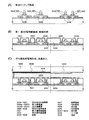
ここで、一般的な表示装置の駆動回路の一例として、デジタル映像入力型式の表示装置におけるソース信号線駆動回路の構成を図10に示す。このソース信号線駆動回路は、クロック信号(S−CK)、クロック反転信号(S−CKb)、スタートパルス(SP)に従って順次サンプリングパルスを出力するパルス出力回路1001を複数段有してなるシフトレジスタ1000と、前記サンプリングパルスの入力に従って、3ビットのデジタル映像信号(Data1〜3)の保持を行う第1のラッチ回路1002、ラッチパルス(Latch Pulse)の入力に従ってデジタル映像信号の保持を行う第2のラッチ回路、デジタル映像信号をアナログ映像信号に変換するためのD/A変換回路1004とを有している。特に図示していないが、バッファ等を有していても良い。また、デジタル映像信号のビット数は3ビットに限定しないことは言うまでもない。
【0007】
動作について簡単に説明する。クロック信号およびスタートパルスの入力に従って、シフトレジスタ1000は、順次サンプリングパルスを出力する。第1のラッチ回路1002においては、サンプリングパルスが入力されるタイミングに従って、デジタル映像信号(Data1〜3)を保持する。この動作が1水平期間分完了した後、水平帰線期間内にラッチパルス(Latch Pulse)が入力され、第1のラッチ回路1002に保持されている1水平周期分のデジタル映像信号は、一斉に第2のラッチ回路1003へと転送される。その後、D/A変換回路1004にデジタル映像信が入力され、各階調に対応した電圧信号へと変換され、ソース信号線(S0001〜S最終)へと書き込まれる。
【0008】
【発明が解決しようとする課題】
このような駆動回路を単極性のTFTを用いて構成する場合について述べる。図5(A)に示しているのは、単極性のTFTによって構成したシフトレジスタである。クロック信号とスタートパルスとに従ってサンプリングパルスを出力するパルス出力回路500を複数段用いて構成される。
【0009】
パルス出力回路単体の回路図を、図5(B)に示す。単極性のTFTによって論理回路を構成する場合、例えばNチャネル型TFTを用いる場合には、高電位側電源に接続したNチャネル型TFTのしきい値により、出力信号の振幅が、入力信号の振幅に比べて減衰するという問題点がある。ここで示したパルス出力回路は、ブートストラップ法によってそのような問題を解決したものであり、同発明者らによって、特願2001−141347号にて出願されているものである。
【0010】
図5(B)に示す回路の動作について簡単に説明する。ここで、回路を構成する単極性のTFTとは、Nチャネル型TFTであるとし、そのしきい値電圧は一律、VthNとする。ただし、これは回路の構成をNチャネル型に限定するものではない。
【0011】
動作について説明する。なお、回路動作の説明をする際に、TFTの動作について述べる場合があるが、TFTがONするとは、TFTのゲート・ソース間電圧の絶対値が、TFTのしきい値電圧の絶対値を超え、TFTのソース領域とドレイン領域とが、チャネル形成領域を通じて導通状態となることをいい、TFTがOFFするとは、TFTのゲート・ソース間電圧の絶対値が、TFTのしきい値電圧の絶対値を下回り、TFTのソース領域とドレイン領域とが非導通状態となることをいうものとする。
【0012】
また、本明細書においては、TFTの接続を説明するのに、「ゲート電極、入力電極、出力電極」と、「ゲート電極、ソース領域、ドレイン領域」とを使い分けている。これは、TFTの動作を説明する際に、ゲート・ソース間電圧を考える場合が多いが、TFTのソース領域とドレイン領域とは、TFTの構造上、明確に区別することが難しいため、信号の入出力を説明する際には、入力電極、出力電極と呼び、TFTの電極の電位の関係について説明する際は、入力電極と出力電極のうちいずれか一方をソース領域、他方をドレイン領域と呼ぶこととする。
【0013】
さらに、説明の際の信号の振幅は、VDD−VSS間とし、高電位側電源をVDD,低電位側電源をVSSとする。また、VthN<(VDD−VthN)を満たすものとする。また、各電位の関係を簡単にするため、VSS=0[V]として考える。ただし、実際に回路を駆動する場合はこの限りでない。
【0014】
あるm段目(1<m≦n)のパルス出力回路において、TFT501、504のゲート電極にはm−1段目の出力パルスが入力されて(m=1、すなわち第1段目の場合、SPが入力される)Hi電位となり、TFT501、504がONする。これにより、TFT505のゲート電極の電位はVDD側に引き上げられ、その電位が(VDD−VthN)となったところでTFT501がOFFし、浮遊状態となる(ただし、VthN<(VDD−VthN))。従ってTFT505がONする。一方、TFT502、503のゲート電極にはこの時点ではパルスが入力されておらず、Lo電位のままであるので、OFFしている。よってTFT506のゲート電極の電位はLo電位であり、OFFしているので、TFT505の入力電極から入力されるCKがHi電位となるのに伴い、出力端子(SR Out)の電位がVDD側に引き上げられる。
【0015】
ここで、TFT505のゲート電極と出力電極間には、容量手段507が設けてあり、さらに今、TFT505のゲート電極は浮遊状態にあるため、出力端子(SR Out)の電位が上昇するのに伴い、ブートストラップによってTFT505のゲート電極の電位は(VDD−VthN)からさらに引き上げられる。これにより、TFT505のゲート電極の電位は、(VDD+VthN)よりも高い電位を取る。よって出力端子(SR Out)の電位は、TFT505のしきい値によって電位が低下することなく、完全にVDDまで上昇する。
【0016】
同様にして、m+1段目においてはS−CKbに従ってパルスが出力される。m+1段目の出力パルスは、m段目に帰還してTFT502、503のゲート電極に入力される。TFT502、503のゲート電極がHi電位となってONすることにより、TFT505のゲート電極の電位はVSS側に引き下げられてTFT505がOFFする。同時にTFT506のゲート電極の電位がHi電位となってONし、m段目の出力端子(SR Out)の電位はLo電位となる。
【0017】
続いて、単極性のTFTによってラッチ回路を構成した例を図6(A)に示す。点線枠601で示す回路が第1のラッチ回路、点線枠602で示す回路が第2のラッチ回路にあたる。点線枠603で示す回路はバッファ回路である。なお、バッファ603の構成に関しては、同発明者らにより、特願2001−133431号にて出願されているものである。
【0018】
第1のラッチ回路601は、TFT604と容量手段605とを有し、TFT604の入力電極には、1ビットのデジタル映像信号(Data)が入力され、TFT604のゲート電極には、サンプリングパルス(Samp.Pulse)が入力される。サンプリングパルスが入力されると、TFT604がONし、デジタル映像信号が容量手段605に保持される。
【0019】
第2のラッチ回路602は、TFT606と容量手段607とを有し、TFT606の入力電極には、第1のラッチ回路にて保持されているデジタル映像信号が入力され、TFT606のゲート電極には、ラッチパルス(Latch Pulse)が入力される。ラッチパルスが入力されると、TFT606がONし、デジタル映像信号が容量手段607に保持される。
【0020】
バッファ603は、TFT608〜611と容量手段612とを有し、TFT609および611のゲート電極には、第2のラッチ回路にて保持されているデジタル映像信号が入力される。TFT608のゲート電極は、電源VDDと接続されている。なお、TFT608の電流能力よりも、TFT609の電流能力を十分に大きく構成している。
【0021】
TFT609および611のゲート電極にHi電位が入力されると、TFT610のゲート電極の電位がLo電位となり、TFT610がOFFする。一方、TFT611がONし、出力端子(Out)にはLo電位が現れる。
【0022】
TFT609および611のゲート電極にLo電位が入力されると、TFT609および611は共にOFFする。よってTFT608を通じて、TFT610のゲート電極の電位が上昇し、その電位が(VDD−VthN)となったところで浮遊状態となる。従ってTFT610がONし、出力端子(Out)の電位が上昇する。それに伴い、容量手段612によるTFT610のゲート電極と出力電極間の容量結合により、TFT610のゲート電極の電位はさらに上昇し、(VDD+VthN)よりも高い電位となる。よって、出力端子(Out)には、Hi電位が現れ、その電位はVDDに等しくなる。
【0023】
なお、第1のラッチ回路601と第2のラッチ回路602との間にはバッファを配置しても良い。
【0024】
ここで、第2のラッチ回路の出力により駆動されるバッファ603に注目する。TFT609にHi電位が入力されてOnしている期間は、VDD−TFT608−TFT609−VSS間に電流パスが生ずる。この電流パスは、第2のラッチ回路からHi電位が出力されている間、電流が流れ続ける。すなわち、ラッチ回路に入力されるデジタル映像信号がHi電位のとき、最大1水平期間にわたって電流が流れ続けることになるため、消費電流の多大な増加を招く。
【0025】
本発明は、回路動作時の消費電流を低減するための回路を提供するものである。
【0026】
【課題を解決するための手段】
前述の課題を解決するために、本発明では以下のような手段を講じた。
【0027】
図6(A)に示したスイッチ用TFT+容量手段の構成によるラッチ回路は、1入力1出力型である。よって、バッファ603も1入力型としている。
【0028】
バッファへの入力信号がHi電位の時、電流パスが生じないようにする方法としては、図6(B)に示すように、 入力信号(In)に対し、反転入力信号(Inb)を用い、TFT608、609が排他的にON、OFFするようにすれば良い。
【0029】
そこで、本発明では、ラッチ回路の出力を、出力、反転出力の2出力型とするような構成とした。
【0030】
本発明の構成を以下に記す。
【0031】
本発明の表示装置の駆動回路は、
第1乃至第3のトランジスタと、第1および第2の容量手段とを有する表示装置の駆動回路であって、
前記第1乃至第3のトランジスタはいずれも同一導電型であり、
前記第1および第2のトランジスタのゲート電極は、第1の信号入力部と電気的に接続され、
前記第1のトランジスタの入力電極は、第2の信号入力部と電気的に接続され、
前記第1のトランジスタの出力電極と、前記第3のトランジスタのゲート電極とは、いずれも第1の信号出力部と電気的に接続され、
前記第2のトランジスタの入力電極は、第1の電源と電気的に接続され、
前記第3のトランジスタの入力電極は、第2の電源と電気的に接続され、
前記第2および第3のトランジスタの出力電極は、いずれも第2の信号出力部と電気的に接続され、
前記第1の容量手段は、前記第1の信号出力部に配置され、前記第1の信号出力部より出力される信号の電位を保持する容量手段であり、
前記第2の容量手段は、前記第2の信号出力部に配置され、前記第2の信号出力部より出力される信号の電位を保持する容量手段であることを特徴としている。
【0032】
本発明の表示装置の駆動回路は、
第1乃至第3のトランジスタと、第1および第2の容量手段とを有する表示装置の駆動回路であって、
前記第1乃至第3のトランジスタはいずれも同一導電型であり、
前記第1および第2のトランジスタのゲート電極は、第1の信号入力部と電気的に接続され、
前記第1のトランジスタの入力電極は、第2の信号入力部と電気的に接続され、
前記第1のトランジスタの出力電極と、前記第3のトランジスタのゲート電極とは、いずれも第1の信号出力部と電気的に接続され、
前記第2のトランジスタの入力電極は、前記第1の信号入力部と電気的に接続され、
前記第3のトランジスタの入力電極は、第2の電源と電気的に接続され、
前記第2および第3のトランジスタの出力電極は、いずれも第2の信号出力部と電気的に接続され、
前記第1の容量手段は、前記第1の信号出力部に配置され、前記第1の信号出力部より出力される信号の電位を保持する容量手段であり、
前記第2の容量手段は、前記第2の信号出力部に配置され、前記第2の信号出力部より出力される信号の電位を保持する容量手段であることを特徴としている。
【0033】
上記の構成によって、デジタル映像信号の入力に対し、非反転出力、反転出力の2出力を得られるため、それらの信号によって駆動される後段のバッファにおいては、電流パスの発生を最小限に抑えることが出来る。よって、表示装置の消費電力の低減に寄与する。
【0034】
本発明の表示装置の駆動回路は、
第1乃至第3のトランジスタと、第1および第2の容量手段と、振幅補償バッファ回路とを有する表示装置の駆動回路であって、
前記第1乃至第3のトランジスタはいずれも同一導電型であり、
前記第1および第2のトランジスタのゲート電極は、第1の信号入力部と電気的に接続され、
前記第1のトランジスタの入力電極は、第2の信号入力部と電気的に接続され、
前記第1のトランジスタの出力電極は、前記第3のトランジスタのゲート電極と電気的に接続され、
前記第2のトランジスタの入力電極は、第1の電源と電気的に接続され、
前記第3のトランジスタの入力電極は、第2の電源と電気的に接続され、
前記第1のトランジスタの出力電極と、第1の信号出力部との間に、前記振幅補償バッファ回路を有し、
前記第2および第3のトランジスタの出力電極と、第2の信号出力部との間に、前記振幅補償バッファ回路を有し、
前記第1の容量手段は、前記第1のトランジスタの出力電極に配置され、前記第1のトランジスタの出力電極より出力される信号の電位を保持する容量手段であり、
前記第2の容量手段は、前記第2および第3のトランジスタの出力電極に配置され、前記第2および第3のトランジスタの出力電極より出力される信号の電位を保持する容量手段であり、
前記振幅補償バッファ回路は、前記第1のトランジスタの出力電極に現れる信号の振幅減衰を補償して、第1の信号出力部に出力し、前記第2および第3のトランジスタの出力電極に現れる信号の振幅減衰を補償して、第2の信号出力部に出力することを特徴としている。
【0035】
本発明の表示装置の駆動回路は、
第1乃至第3のトランジスタと、第1および第2の容量手段と、振幅補償バッファ回路とを有する表示装置の駆動回路であって、
前記第1乃至第3のトランジスタはいずれも同一導電型であり、
前記第1および第2のトランジスタのゲート電極は、第1の信号入力部と電気的に接続され、
前記第1のトランジスタの入力電極は、第2の信号入力部と電気的に接続され、
前記第1のトランジスタの出力電極は、前記第3のトランジスタのゲート電極と電気的に接続され、
前記第2のトランジスタの入力電極は、前記第1の信号入力部と電気的に接続され、
前記第3のトランジスタの入力電極は、第2の電源と電気的に接続され、
前記第1のトランジスタの出力電極と、第1の信号出力部との間に、前記振幅補償バッファ回路を有し、
前記第2および第3のトランジスタの出力電極と、第2の信号出力部との間に、前記振幅補償バッファ回路を有し、
前記第1の容量手段は、前記第1のトランジスタの出力電極に配置され、前記第1のトランジスタの出力電極より出力される信号の電位を保持する容量手段であり、
前記第2の容量手段は、前記第2および第3のトランジスタの出力電極に配置され、前記第2および第3のトランジスタの出力電極より出力される信号の電位を保持する容量手段であり、
前記振幅補償バッファ回路は、前記第1のトランジスタの出力電極に現れる信号の振幅減衰を補償して、第1の信号出力部に出力し、前記第2および第3のトランジスタの出力電極に現れる信号の振幅減衰を補償して、第2の信号出力部に出力することを特徴としている。
【0036】
本発明の表示装置の駆動回路は、
第1乃至第7のトランジスタと、第1乃至第4の容量手段とを有する表示装置の駆動回路であって、
前記第1乃至第7のトランジスタはいずれも同一導電型であり、
前記第1および第2のトランジスタのゲート電極は、第1の信号入力部と電気的に接続され、
前記第1のトランジスタの入力電極は、第2の信号入力部と電気的に接続され、
前記第1のトランジスタの出力電極は、前記第3のトランジスタのゲート電極、前記第4のトランジスタのゲート電極、および前記第5のトランジスタのゲート電極と電気的に接続され、
前記第2のトランジスタの入力電極は、第1の電源と電気的に接続され、
前記第3のトランジスタの入力電極は、第2の電源と電気的に接続され、
前記第2のトランジスタの出力電極は、前記第3のトランジスタの出力電極、前記第6のトランジスタのゲート電極、および前記第7のトランジスタのゲート電極と電気的に接続され、
前記第4のトランジスタの入力電極、および前記第7のトランジスタの入力電極は、前記第1の電源と電気的に接続され、
前記第5のトランジスタの入力電極、および前記第6のトランジスタの入力電極は、前記第2の電源と電気的に接続され、
前記第4のトランジスタの出力電極と、前記第6のトランジスタの出力電極とは、いずれも第1の信号出力部と電気的に接続され、
前記第5のトランジスタの出力電極と、前記第7のトランジスタの出力電極とは、いずれも第2の信号出力部と電気的に接続され、
前記第1の容量手段は、前記第1のトランジスタの出力電極に配置され、前記第1のトランジスタの出力電極より出力される信号の電位を保持する容量手段であり、
前記第2の容量手段は、前記第2および第3のトランジスタの出力電極に配置され、前記第2および第3のトランジスタの出力電極より出力される信号の電位を保持する容量手段であり、
前記第3の容量手段は、前記第4のトランジスタのゲート電極と出力電極との間に配置されて容量結合を形成する容量手段であり、
前記第4の容量手段は、前記第7のトランジスタのゲート電極と出力電極との間に配置されて容量結合を形成する容量手段であることを特徴としている。
【0037】
本発明の表示装置の駆動回路は、
第1乃至第7のトランジスタと、第1乃至第4の容量手段とを有する表示装置の駆動回路であって、
前記第1乃至第7のトランジスタはいずれも同一導電型であり、
前記第1および第2のトランジスタのゲート電極は、第1の信号入力部と電気的に接続され、
前記第1のトランジスタの入力電極は、第2の信号入力部と電気的に接続され、
前記第1のトランジスタの出力電極は、前記第3のトランジスタのゲート電極、前記第4のトランジスタのゲート電極、および前記第5のトランジスタのゲート電極と電気的に接続され、
前記第2のトランジスタの入力電極は、前記第1の信号入力部と電気的に接続され、
前記第3のトランジスタの入力電極は、第2の電源と電気的に接続され、
前記第2のトランジスタの出力電極は、前記第3のトランジスタの出力電極、前記第6のトランジスタのゲート電極、および前記第7のトランジスタのゲート電極と電気的に接続され、
前記第4のトランジスタの入力電極、および前記第7のトランジスタの入力電極は、前記第1の電源と電気的に接続され、
前記第5のトランジスタの入力電極、および前記第6のトランジスタの入力電極は、前記第2の電源と電気的に接続され、
前記第4のトランジスタの出力電極と、前記第6のトランジスタの出力電極とは、いずれも第1の信号出力部と電気的に接続され、
前記第5のトランジスタの出力電極と、前記第7のトランジスタの出力電極とは、いずれも第2の信号出力部と電気的に接続され、
前記第1の容量手段は、前記第1のトランジスタの出力電極に配置され、前記第1のトランジスタの出力電極より出力される信号の電位を保持する容量手段であり、
前記第2の容量手段は、前記第2および第3のトランジスタの出力電極に配置され、前記第2および第3のトランジスタの出力電極より出力される信号の電位を保持する容量手段であり、
前記第3の容量手段は、前記第4のトランジスタのゲート電極と出力電極との間に配置されて容量結合を形成する容量手段であり、
前記第4の容量手段は、前記第7のトランジスタのゲート電極と出力電極との間に配置されて容量結合を形成する容量手段であることを特徴としている。
【0038】
上記の構成によって、デジタル映像信号の入力に対し、非反転出力、反転出力の2出力を得られるため、それらの信号によって駆動される後段のバッファにおいては、電流パスの発生を最小限に抑えることが出来る。よって、表示装置の消費電力の低減に寄与する。
【0039】
さらに、第1のトランジスタの出力電極から得られる非反転出力信号と、第2および第3のトランジスタの出力電極から得られる反転出力信号とは、ブートストラップによる振幅補償を受けるため、回路の動作をより確実にすることが出来る。
【0040】
本発明によると、
請求項1乃至請求項6のいずれか1項において、
前記第2の信号出力部より出力される信号は、前記第1の信号出力部より出力される信号の反転信号であっても良い。
【0041】
本発明によると、
請求項1乃至請求項7のいずれか1項において、
前記導電型とは、Nチャネル型であっても良い。
【0042】
本発明によると、
請求項1乃至請求項7のいずれか1項において、
前記導電型とは、Pチャネル型であっても良い。
【0043】
本発明によると、
請求項1乃至請求項9のいずれか1項において、
前記第1乃至第4の容量手段は、トランジスタのゲート電極と入力電極との間、もしくはトランジスタのゲート電極と出力電極との間の容量を用いた容量手段であっても良い。
【0044】
本発明によると、
請求項1乃至請求項9のいずれか1項において、
前記第1乃至第4の容量手段は、半導体層を形成する材料、ゲート電極を形成する材料、配線材料のうちいずれか2材料と、前記2材料間の絶縁膜とでなる容量手段であっても良い。
【発明の実施の形態】
図1に示すのは、本発明のラッチ回路の構成であり、TFT101〜103、および容量手段104、105を有する。TFT101、102のゲート電極には、シフトレジスタより出力されるサンプリングパルス(Samp.Pulse)が入力され、TFT101の入力電極には,デジタル映像信号(DigitalData)が入力される。TFT102の入力電極は、高電位側電源VDDに接続され、TFT103の入力電極は、低電位側電源VSSに接続されている。
【0045】
この構成の特徴としては、デジタル映像信号の入力に対し、出力(Data Out)、反転出力(Data Out_b)の2出力を得る点である。
【0046】
回路の動作について説明する。なお、サンプリングパルスおよびデジタル映像信号の、入力時の振幅はいずれもVDD−VSS間とする。
【0047】
シフトレジスタより出力されたサンプリングパルスが、TFT101、102のゲート電極に入力され、TFT101、102がONする。入力されているデジタル映像信号がHi電位のとき、TFT103のゲート電極にHi電位が入力されてONする。このとき、TFT102、103がともにONしているが、TFT103の電流能力を、TFT102の電流能力よりも十分に高くしておくことにより、TFT102、103の出力電極、つまり反転出力端子(Data Out_b)にはLo電位が現れる。出力端子(Data Out)には、デジタル映像信号がTFT101を通じてそのまま出力される。
【0048】
一方、入力されているデジタル映像信号がLo電位のとき、TFT103のゲート電極にはLo電位が入力されてOFFする。よって、反転出力端子(Data Out_b)にはHi電位が現れる。出力端子(Data Out)には、デジタル映像信号がTFT101を通じてそのまま出力される。
【0049】
以上の動作が順次、1水平周期分行われる。出力端子(Data Out)および反転出力端子(Data Out_b)に出力された信号は、それぞれ容量手段104、105によって、帰線期間までの間、保持される。
【0050】
サンプリングパルス(Samp.Pulse)がLo電位となり、サンプリング期間が終了すると、TFT101、102がOFFする。つまり、図1に示した本発明のラッチ回路においては、VDD−TFT102−TFT103−VSS間に電流パスが生ずるのは、サンプリングパルスが入力されており、かつデジタル映像信号がHi電位の時に限られる。
【0051】
ここで、出力端子(Data Out)側に現れる出力信号の振幅は、TFT101のしきい値の影響を受けるため、(VDD−VthN)−VSS間となり、反転出力端子(Data Out_b)側に現れる出力信号の振幅は、TFT102のしきい値の影響を受けるため、同様に(VDD−VthN)−VSS間となるが、以後、ラッチ回路の後段にバッファを設けることにより、ブートストラップを用いて振幅の補償を行うため、問題とはならない。
【0052】
【実施例】
以下に、本発明の実施例について記載する。
【0053】
[実施例1]
図11は、実施形態にて説明した構成でなる回路を第1のラッチ回路とし、第2のラッチ回路およびバッファまでを構成した例である。第1のラッチ回路111は、TFT114〜116および容量手段117、118とを有し、第2のラッチ回路112は、TFT119、120および容量手段121、122とを有し、バッファ回路113は、TFT123〜126および容量手段127でなるインバータと、TFT128〜131および容量手段132でなるインバータとを有する。
【0054】
1水平周期分のサンプリングが終了した後の帰線期間中に、ラッチパルス(Latch Pulse)が入力されると、第2のラッチ回路112におけるTFT119、120がONし、第1のラッチ回路111において、容量手段117、118にて保持されている信号が、第2のラッチ回路112における容量手段121、122に書き込まれる。
【0055】
サンプリングパルス(Samp.Pulse)がLo電位となり、サンプリング期間が終了すると、TFT114、115がOFFし、TFT116もまたOFFする。よって、TFT119、120の入力電極は浮遊状態となる。続いて、ラッチパルス(Latch Pulse)が入力されると、TFT119、120がONし、容量手段121、122に信号が書き込まれるが、このとき、TFT119、120の入力電極に電流の供給源が接続されていないため、前述の動作は、容量手段117、118、121、122における電荷の移動のみによって行われることになる。よって容量手段121、122への書き込みが十分に行われるようにするためには、容量手段117、118は大きく設計しておくのが望ましい。
【0056】
続いて、第2のラッチ回路112からの出力信号は、バッファ回路113へと入力される。バッファ回路113は、2つのインバータを対に配置したものであるので、ここでは、TFT123〜126および容量手段127で構成されたインバータ一方のみの動作について述べる。
【0057】
第2のラッチ回路112の一方の出力(Data Out2)がHi電位のとき、TFT123のゲート電極にHi電位が入力されてONする。一方、TFT124、126のゲート電極には、第2のラッチ回路112の他方の出力(Data Out2_b)であるLo電位が入力されてOFFする。よって、TFT125のゲート電極の電位が上昇する。
【0058】
今、TFT123のゲート電極の電位は、(VDD−VthN)であるので、TFT125のゲート電極の電位が(VDD−VthN)となったところで、TFT123のゲート・ソース間電圧がそのしきい値を下回り、OFFする。よってTFT125のゲート電極は、その時点で一時浮遊状態となる。
【0059】
ここで、VthN<(VDD−VthN)であるならば、TFT125がONし、バッファ113の出力端子(Data Out3)にはHi電位が現れるので、電位が上昇する。さらに、TFT125のゲート電極と出力電極との間には容量手段127を有し、今、TFT125のゲート電極は浮遊状態であるので、出力端子(Data Out3)の電位上昇に伴い、容量結合によってTFT125のゲート電極の電位がさらに上昇する。
【0060】
結果、TFT125のゲート電極の電位が、(VDD+VthN)よりも高くなると、出力端子にHi電位が現れ、その電位はTFT125のしきい値の影響を受けることなく、VDDに等しくなる。
【0061】
一方、第2のラッチ回路112の一方の出力(Data Out2)がLo電位のとき、TFT123のゲート電極にはLo電位が入力されてOFFする。一方、TFT124、126のゲート電極には、第2のラッチ回路112の他方の出力(Data Out2_b)であるHi電位が入力されてONする。よってTFT125のゲート電極の電位はLo電位となってOFFし、出力端子(Data
Out3)にはLo電位が現れる。
【0062】
TFT128〜131および容量手段132でなるインバータについても動作は同様であり、一方の出力端子(Data Out3)にHi電位が現れるときは、他方の出力端子(Data Out3_b)にはLo電位が現れる。
【0063】
本実施例で示したラッチ回路においては、第1のラッチ回路〜第2のラッチ回路において、TFTのしきい値分の振幅減衰が生ずるため、電源電圧がある程度高い必要がある。そこで、第1のラッチ回路の出力を、一旦バッファを介して振幅の補償を行う構成としても良い。
【0064】
[実施例2]
本実施例においては、同一基板上に、画素部および、画素部周辺に設ける駆動回路のTFTを同時に作製する方法について説明する。なお、例として液晶表示装置の作製工程を挙げるが、本発明は前述のとおり、液晶表示装置に限定されない。
【0065】
まず、図7(A)に示すように、コーニング社の#7059ガラスや#1737ガラス等に代表されるバリウムホウケイ酸ガラス、またはアルミノホウケイ酸ガラス等からなる基盤5001上に酸化シリコン膜、窒化シリコン膜、または酸化窒化シリコン膜等の絶縁膜からなる下地膜5002を形成する。特に図示していないが、下地膜5002の形成については、例えば、プラズマCVD法でSiH4、NH3、N2Oから作製される酸化窒化シリコン膜を10〜200[nm](好ましくは50〜100[nm])の厚さに形成し、同様にSiH4、N2Oから作製される酸化窒化水素化シリコン膜を50〜200[nm](好ましくは100〜150[nm])の厚さに積層形成する。
【0066】
続いて、島状の半導体層5003〜5005は、非晶質構造を有する半導体膜を。レーザー結晶化法や公知の熱結晶化法を用いて作製した結晶質半導体膜で形成する。この島状の半導体層5003〜5005の厚さは25〜80[nm](好ましくは30〜60[nm])として形成する。結晶質半導体層の材料には特に限定は無いが、好ましくはシリコンまたはシリコンゲルマニウム(SiGe)合金等で形成すると良い。
【0067】
レーザー結晶化法で結晶質半導体膜を作製するには、パルス発振型または連続発光型のエキシマレーザーやYAGレーザー、YVO4レーザーを用いる。これらのレーザーを用いる場合には、レーザー発振器から放射されたレーザー光を光学系で線状に集光して半導体膜に照射する方法を用いると良い。結晶化の条件は実施者が適宜選択するものであるが、エキシマレーザーを用いる場合にはパルス発振周波数を30[Hz]とし、レーザーエネルギー密度を100〜400[mJ/cm2](代表的には200〜300[mJ/cm2])とする。また、YAGレーザーを用いる場合にはその第2高調波を用い、パルス発振周波数1〜10[kHz]とし、レーザーエネルギー密度を300〜600[mJ/cm2](代表的には350〜500[mJ/cm2])とすると良い。そして幅100〜1000[μm]、例えば400[μm]で線状に集光したレーザー光を基板全面に渡って照射し、このときの線状レーザーの重ねあわせ率(オーバーラップ率)を80〜98[%]として行う。
【0068】
続いて、島状の半導体層5003〜5005を覆うゲート絶縁膜5006を形成する。ゲート絶縁膜5006は、プラズマCVD法またはスパッタ法を用い、厚さを40〜150[nm]としてシリコンを含む絶縁膜で形成する。本実施例では、120[nm]の厚さで酸化窒化シリコン膜で形成する。勿論、ゲート絶縁膜はこのような酸化窒化シリコン膜に限定されるものではなく、他のシリコンを含む絶縁膜を単層または積層構造として用いても良い。例えば、酸化シリコンを用いる場合には、プラズマCVD法でTEOS(Tetraethyl Orthosilicate)とO2とを混合し、反応圧力40[Pa]、基板温度300〜400[℃]とし、高周波(13.56[MHz])電力密度0.5〜0.8[W/cm2]で放電させて形成することが出来る。このようにして作製される酸化シリコン膜は、その後400〜500[℃]の熱アニールにより、ゲート絶縁膜として良好な特性を得ることが出来る。
【0069】
そして、ゲート絶縁膜5006上にゲート電極を形成するための第1の導電膜5007と第2の導電膜5008とを積層形成する。本実施例では、第1の導電層5007をタンタル(Ta)で50〜100[nm]の厚さに形成し、第2の導電層5009をタングステン(W)で100〜300[nm]の厚さに形成する(図7(A))。
【0070】
Ta膜はスパッタ法で、TaのターゲットをArでスパッタすることにより形成する。この場合、Arに適量のXeやKrを加えると、Ta膜の内部応力を緩和して膜の剥離を防止することが出来る。また、α相のTa膜の抵抗率は20[μΩcm]程度でありゲート電極として使用することが出来るが、β相のTa膜の抵抗率は180[μΩcm]程度でありゲート電極には不向きである。α相のTa膜を形成するために、Taのα相に近い結晶構造を有する窒化タンタル(TaN)を10〜50[nm]程度の厚さでTaの下地に形成しておくとα相のTa膜を容易に得ることが出来る。
【0071】
W膜を形成する場合には、Wをターゲットとしたスパッタ法で形成する。その他にも6フッ化タングステン(WF6)を用いる熱CVD法で形成することも出来る。いずれにしてもゲート電極として使用するためには低抵抗化を図る必要があり、W膜の抵抗率は20[μΩcm]以下にすることが望ましい。W膜は結晶粒を大きくすることで低抵抗率化を図ることが出来るが、W中に酸素などの不純物元素が多い場合には結晶化が阻害されて高抵抗化する。このことより、スパッタ法による場合、純度99.9999[%]のWターゲットを用い、さらに製膜時に気相中からの不純物の混入がないように十分配慮してW膜を形成することにより、抵抗率9〜20[μΩcm]を実現することが出来る。
【0072】
なお、本実施例においては、第1の導電膜5007をTa、第2の導電膜5008をWとしたが、特に限定されず、いずれもTa、W、Mo、Al、Cuから選ばれた元素、または前記元素を主成分とする合金材料もしくは化合物材料で形成しても良い。また、リン等の不純物元素をドーピングした多結晶シリコン膜に代表される半導体膜を用いても良い。本実施例以外の他の組み合わせの一例としては、第1の導電膜をTaN、第2の導電膜をWとする組み合わせ、第1の導電膜をTaN、第2の導電膜をAlとする組み合わせ、第1の導電膜をTaN、第2の導電膜をCuとする組み合わせ等が望ましい。
【0073】
次に、レジストによるマスク5009を形成し、電極および配線を形成するための第1のエッチング処理を行う。本実施例ではICP(Inductively coupled plasma:誘導結合型プラズマ)エッチング法を用い、エッチング用ガスにCF4とCl2とを混合し、1[Pa]の圧力でコイル型の電極に500[W]のRF(13.56[MHz])電力を投入してプラズマを生成して行う。基板側(試料ステージ)にも100[W]のRF電力を投入し、実質的に負の自己バイアス電圧を印加する。CF4とCl2とを混合した場合にはW膜およびTa膜とも同程度にエッチングされる。
【0074】
上記エッチング条件では、レジストによるマスクの形状を適したものとすることと、基板側に印加するバイアス電圧の効果とにより第1の導電膜および第2の導電膜の端部がテーパー形状となる。テーパー部の角度は15〜45°となる。ゲート絶縁膜上に残渣を残すことなくエッチングを行うためには、10〜20[%]の割合でエッチング時間を増加させると良い。W膜に対する酸化窒化シリコン膜の選択比は2〜4(代表的には3)であるので、オーバーエッチング処理により、酸化窒化シリコン膜が露出した面は20〜50[nm]程度エッチングされることになる。こうして、第1のエッチング処理により第1の導電層5010a〜5013aと第2の導電層5010b〜5013bからなる第1の形状の導電層5010〜5013を形成する。このとき、ゲート絶縁膜5006においては、第1の形状の導電層5010〜5013で覆われない領域は20〜50[nm]程度エッチングされて薄くなった領域が形成される(図7(B))。
【0075】
そして、第1のドーピング処理を行い、N型を付与する不純物元素を添加する(図7(B))。ドーピング処理は、イオンドーピング法もしくはイオン注入法で行えば良い。イオンドープ法にあたっての条件は、ドーズ量を1×10¹³〜5×10¹⁴[atoms/cm2]とし、加速電圧を60〜100[keV]とする。N型を付与する不純物元素としては、15族に属する元素、典型的にはリン(P)または砒素(As)を用いるが、ここではPを用いる。この場合、導電層5010〜5013がN型を付与する不純物元素に対するマスクとなり、自己整合的に第1の不純物領域5014〜5016が形成される。この第1の不純物領域5014〜5016には、1×1020〜1×1021[atoms/cm3]の濃度範囲でN型を付与する不純物元素を添加する。
【0076】
次に、第2のエッチング処理を行う(図7(C))。同様にICPエッチング法を用い、エッチング用ガスにCF4とCl2とO2とを混合して、1[Pa]の圧力でコイル型の電極に500[W]のRF電力を供給し、プラズマを生成して行う。基板側(試料ステージ)にも50[W]のRF電力を投入し、第1のエッチング処理に比べ低い自己バイアス電圧を印加する。このような条件により第2の導電層であるWを異方性エッチングし、かつ、それより遅いエッチング速度で第1の導電層であるTaを異方性エッチングして第2の形状の導電層5017〜5020(第1の導電層5017a〜5020aおよび第2の導電層5017b〜5020b)を形成する。このとき、ゲート絶縁膜5006においては、第2の形状の導電層5017〜5020で覆われない領域はさらに20〜50[nm]程度エッチングされて薄くなった領域が形成される。
【0077】
W膜やTa膜のCF4とCl2の混合ガスによるエッチング反応は、生成されるラジカルまたはイオン種と反応生成物の蒸気圧から推測することが出来る。WとTaのフッ化物と塩化物の蒸気圧を比較すると、Wのフッ化物であるWF6の蒸気圧が極端に高く、その他のWCl5、TaF5、TaCl5については同程度である。従って、CF4とCl2の混合ガスでは、W膜およびTa膜共にエッチングされる。しかし、この混合ガスに適量のO2を添加するとCF4とO2が反応してCOとFになり、FラジカルまたはFイオンが多量に発生する。その結果、フッ化物の蒸気圧が高いW膜のエッチング速度が増大する。一方、TaはFが増大しても、相対的にエッチング速度の増加は少ない。また、TaはWに比較して酸化されやすいので、O2を添加することでTaの表面が酸化される。Taの酸化物はフッ素や塩素と反応しないため、さらにTa膜のエッチング速度は低下することとなる。従って、W膜とTa膜とのエッチング速度に差を作ることが可能となる。
【0078】
そして、第2のドーピング処理を行う(図7(C))。この場合、第1のドーピング処理よりもドーズ量を下げて高い加速電圧の条件としてN型を付与する不純物元素ドーピングする。例えば、加速電圧を70〜120[keV]とし、1×10¹³[atoms/cm2]のドーズ量で行い、図7(B)で島状の半導体層に形成された第1の不純物領域の内側に新たな不純物領域を形成する。ドーピングは、第2の導電層5017b〜5020bを不純物元素に対するマスクとして用い、第1の導電層5017a〜5020aの下側の領域にも不純物元素が添加されるようにしてドーピングする。
こうして、第1の導電層と重なる第2の不純物領域5021〜5023が形成される。
【0079】
続いて、第3のエッチング処理を行う(図8(A))。ここでは、エッチング用ガスにCl2を用い、ICPエッチング装置を用いて行う。本実施例では、Cl2のガス流量比を60[sccm]とし、1 [Pa]の圧力でコイル型の電極に350[W]のRF電力を投入してプラズマを生成してエッチングを70秒行った。基板側(試料ステージ)にもRF電力を投入し、実質的に負の自己バイアス電圧を印加する。第3のエッチングにより、第1の導電層が後退して第3の形状の導電層5024〜5027(第1の導電層5024a〜5027aおよび第2の導電層5024b〜5027b)が形成され、第2の不純物領域5021〜5023の一部は、第1の導電層と重ならない第3の不純物領域5028〜5030となる。
【0080】
以上までの工程でそれぞれの島状の半導体層に不純物領域が形成される。島状の半導体層と重なる第3の形状の導電層5024〜5027が、TFTのゲート電極として機能する。
【0081】
続いて、導電型の制御を目的として、それぞれの島状の半導体層に添加された不純物元素を活性化する工程を行う。この工程はファーネスアニール炉を用いる熱アニール法で行う。その他に、レーザーアニール法、ラピッドサーマルアニール法(RTA法)を適用することが出来る。熱アニール法では酸素濃度が1[ppm]以下、好ましくは0.1[ppm]以下の窒素雰囲気中で400〜700[℃]、代表的には500〜600[℃]で行うものであり、本実施例では500[℃]で4時間の熱処理を行う。ただし、5024〜5027に用いた配線材料が熱に弱い場合には、配線等を保護するため層間絶縁膜(シリコンを主成分とする)を形成した後で熱活性化を行うことが望ましい。
【0082】
さらに、3〜100[%]の水素を含む雰囲気中で、300〜450[℃]で1〜12時間の熱処理を行い、島状の半導体層を水素化する工程を行う。この工程は熱的に励起された水素により半導体層のダングリングボンドを終端する工程である。水素化するための、熱水素化の他の方法として、プラズマ水素化(プラズマにより励起された水素を用いる)によって行っても良い。
【0083】
次いで、図8(B)に示すように、第1の層間絶縁膜5031を、酸化窒化シリコン膜で100〜200[nm]の厚さで形成する。その上に有機絶縁物材料からなる第2の層間絶縁膜5032を形成した後、第1の層間絶縁膜5031、第2の層間絶縁膜5032、およびゲート絶縁膜5006に対してコンタクトホールを開口し、配線材料による膜を形成して各配線5033〜5036、および画素電極5037をパターニング形成する。
【0084】
第2の層間絶縁膜5032としては、ポリイミド、ポリアミド、アクリル、BCB(ベンゾシクロブテン)等の有機樹脂を材料とする膜を用いる。特に、第2の層間絶縁膜5032は平坦化の意味合いが強いので、平坦性に優れたアクリルが望ましい。本実施例ではTFTによって形成される段差を十分に平坦化しうる膜厚でアクリル膜を形成する。好ましくは1〜5[μm](さらに好ましくは2〜4[μm])とすれば良い。
【0085】
コンタクトホールの形成は、ドライエッチングまたはウェットエッチング法を用い、N型の不純物領域5014〜5016、およびソース信号線(図示せず)、ゲート信号線(図示せず)、電流供給線(図示せず)およびゲート電極5024〜5026に達する(図示せず)コンタクトホールをそれぞれ形成する。
【0086】
また、配線5033〜5036として、Ti膜を100[nm]、Tiを含むAl膜を300[nm]、Ti膜を150[nm]、スパッタ法で連続形成した3層積層の膜を所望の形状にパターニングして形成する。勿論、他の導電性材料を用いても良い。画素電極5037については、表示装置を反射型とする場合には、反射性の高い材料にて形成する。この場合、配線と同時に形成しても良い。一方、透過型である場合には、酸化インジウム錫(Indium Tin Oxide:ITO)等の透明導電性材料を用いて形成する。図8(B)の状態まで完了したものを、本明細書ではアクティブマトリクス基板と呼ぶ。
【0087】
続いて、対向基板5038を用意する。対向基板5038には、遮光膜5039が形成される。この遮光膜は、クロム(Cr)等を用いて、100[nm]〜200[nm]の厚さで形成する。
【0088】
一方、画素部においては対向電極5040が形成される。対向電極は、ITO等の透明導電性材料を用いて形成する。また、可視光の透過率を高く保つために、対向電極の膜厚は100[nm]〜120[nm]で形成することが望ましい。
【0089】
アクティブマトリクス基板と対向基板とに、配向膜5041、5042を形成する。配向膜5041、5042の膜厚は、30[nm]〜80[nm]が望ましい。また、配向膜としては、例えば日産化学社製SE7792等を用いることが出来る。プレチルト角の高い配向膜を用いると、アクティブマトリクス方式により駆動される液晶表示装置の駆動時に、ディスクリネーションの発生を抑制することが出来る。
【0090】
続いて、配向膜5041、5042をラビングする。ラビング方向は、液晶表示装置が完成したときに、左巻きのTN(Twisted Nematic)配向となるようにするのが望ましい。
【0091】
本実施例においては特に図示していないが、スペーサを画素内に散布もしくはパターニングにより形成して、セルギャップの均一性を向上させることも可能である。本実施例においては、感光性樹脂膜を製膜、パターニングして、4.0[μm]の高さのスペーサを形成した。
【0092】
続いて、シール剤5043により、アクティブマトリクス基板と対向基板とを貼り合わせる。シール剤としては、熱硬化型のシール剤である三井化学社製XN−21Sを用いた。シール剤中にはフィラーを混入する。なお、フィラーの高さは4.0[μm]とする。その後、シール剤が硬化した後に、アクティブマトリクス基板と対向基板とを、所望のサイズに同時に分断する。
【0093】
続いて、液晶5044を注入する。液晶材料としては、高速応答性等を考慮すると、低粘度のものが望ましい。本実施例においては、配向制御の容易なネマチック液晶を用いる。勿論、高速応答が可能な強誘電性液晶、反強誘電性液晶を用いても良い。
【0094】
液晶の注入が終了したのち、注入口をUV硬化型樹脂等を用いて封止する。その後、公知の方法により偏光板を貼り付ける。最後に、基板上に形成された素子又は回路から引き回された端子と外部信号端子とを接続するためのコネクタ(フレキシブルプリントサーキット:FPC)を取り付けて製品として完成する(図8(C))。このような出荷出来る状態にまでした状態を本明細書中では液晶表示装置と呼ぶ。
【0095】
また、本実施例で示す工程に従えば、アクティブマトリクス基板の作製に必要なフォトマスクの数を4枚(島状半導体層パターン、第1配線パターン(ゲート配線、島状のソース配線、容量配線)、コンタクトホールパターン、第2配線パターン(画素電極、接続電極含む))とすることができる。その結果、工程を短縮し、製造コストの低減及び歩留まりの向上に寄与することができる。
【0096】
なお、本実施例においては、TFTの型式としてはトップゲート型TFTを例に挙げて説明しているが、その他に、図17(A)に示すような活性層の下側にゲート電極を形成したボトムゲート型TFT、あるいは図17(B)に示すような、活性層を挟み込むように、上下にゲート電極を有するデュアルゲート型TFTを用いても実施が可能である。
【0097】
[実施例3]
本実施例においては、実施形態および実施例1に示した回路を用いて、実際に表示装置を作製した例について述べる。
【0098】
図2(A)に、表示装置の概略図を示す。基板200の中央部に、画素部201が配置されている。画素部201の周辺には、ソース信号線を制御するための、ソース信号線駆動回路202および、ゲート信号線を制御するための、ゲート信号線駆動回路207が配置されている。ゲート信号線駆動回路207は、図2(A)では画素部201の両側に対称配置されているが、画素部201の片側のみに配置しても良い。
【0099】
ソース信号線駆動回路202、ゲート信号線駆動回路207を駆動するために外部より入力される信号は、FPC210を介して入力される。本実施例においては、FPC210より入力される信号は、その電圧振幅が小さいため、本実施例では、レベルシフタ206によって電圧振幅の変換を受けた上で、ソース信号線駆動回路202、およびゲート信号線駆動回路207へと入力される。
【0100】
図2(A)において、破線A−A'の断面図を図2(B)に示す。基板200上には、画素部201、ソース信号線駆動回路202、ゲート信号線駆動回路(図示せず)が形成されている。基板200と、対向基板211とは、シール剤212を用いて貼り合わされ,基板間のギャップには液晶が注入される。液晶の注入後は、図2(A)に示すように、封止剤213によって、注入口を密閉する。
【0101】
引き回し配線221は、異方導電性フィルム223を介して、FPC210が有するFPC側配線222と電気的に接続される。異方導電性フィルム223には、図2(C)に示すように導電性のフィラー224が含まれており、基板200とFPC210とを熱圧着することで、基板200上の引き回し配線221と、FPC210上のFPC側配線222とが、導電性フィラー224によって電気的に接続される。
【0102】
ソース信号線駆動回路202の構成を図3に示す。点線枠300で示されるシフトレジスタは、クロック信号とスタートパルスとに従ってサンプリングパルスを出力するパルス出力回路301を複数段用いて構成される。第1のラッチ回路302〜第2のラッチ回路303〜バッファ回路304は、実施例1にて図11に示したものを用いている。図3のソース信号線駆動回路には、3ビットのデジタル映像信号(Data1〜Data3)が入力される。よって、第1のラッチ回路302〜第2のラッチ回路303〜バッファ回路304は、3組が並列に配置され、1つのパルス出力回路から出力されるサンプリングパルスによって、同時に3ビットのデジタル映像信号の保持を行う。
【0103】
D/A変換回路305に関しては、本明細書では特に図示していないが、従来用いられている抵抗分割型、容量型等、いずれの型式のものを用いても良い。
【0104】
D/A変換回路305にて、3ビットのデジタル映像信号は23階調のアナログ映像信号へと変換され、それぞれ、ソース信号線(S0001〜S最終)へと書き込まれる。
【0105】
なお、外部より入力される信号は、IC等の集積回路より出力されるため、近年の低電圧化に伴い、3[V]〜5[V]程度の低電圧振幅の信号である場合が多いため、それぞれのレベルシフタ306〜309によって、高電圧振幅の信号へと変換された後、駆動回路へと入力される。
【0106】
ゲート信号線駆動回路203の構成を図4に示す。点線枠300で示されるシフトレジスタは、クロック信号とスタートパルスとに従ってゲート信号線選択パルスを出力するパルス出力回路301を複数段用いて構成される。ゲート信号線の負荷が大きい場合には、すなわち、シフトレジスタより出力されるゲート信号線選択パルスが、直接ゲート信号線の電位をHi電位、Lo電位と切り替えるだけの駆動能力を有していない場合、バッファ404を用いる必要がある。
【0107】
なお、外部より入力される信号は、IC等の集積回路より出力されるため、近年の低電圧化に伴い、3[V]〜5[V]程度の低電圧振幅の信号である場合が多いため、それぞれのレベルシフタ401、402によって、高電圧振幅の信号へと変換された後、駆動回路へと入力される。
【0108】
[実施例4]
実施例2に示した工程は、画素および周辺の駆動回路をNチャネル型TFTを用いて構成する場合の例として説明したが、本発明はPチャネル型TFTを用いての実施も可能である、
【0109】
Nチャネル型TFTの場合、ホットキャリア劣化等の抑制のため、ゲート電極と重なる領域に、オーバーラップ領域と呼ばれる不純物領域を設けている。これに対してPチャネル型TFTの場合は、ホットキャリア劣化による影響が小さいので、特にオーバーラップ領域を設ける必要はなく、この場合、より簡単な工程で作製することが可能である。
【0110】
図9(A)に示すように、実施例4に従って、ガラス等の絶縁基板6001上に下地膜6002を形成し、次いで島状の半導体層6003〜6005、ゲート絶縁膜6006、導電層6007、6008を形成する。ここで、導電層6007、6008は、ここでは積層構造としているが、特に単層であっても構わない。
【0111】
次いで、図9(B)に示すように、レジストによるマスク6009を形成し、第1のエッチング処理を行う。実施例4においては、積層構造とした導電層の材質による選択比を利用して、異方性エッチングを行ったが、ここでは特にオーバーラップ領域となる領域を設ける必要はないので、通常エッチングにて行えば良い。このとき、ゲート絶縁膜6006においては、エッチングによって20[nm]〜50[nm]程度薄くなった領域が形成される。
【0112】
続いて、島状の半導体層にP型を付与する不純物元素を添加するための第1のドーピング処理を行う。導電層6010〜6013を不純物元素に対するマスクとして用い、自己整合的に不純物領域を形成する。P型を付与する不純物元素としては、ボロン(B)等が代表的である。ここでは、ジボラン(B2H6)を用いたイオンドープ法で形成し、半導体層中の不純物濃度が2×10²⁰〜2×10²¹[atoms/cm3]となるようにする。
【0113】
レジストによるマスクを除去して、図9(C)の状態を得る。以後、実施例2における図8(B)以降の工程に従って作製する。
【0114】
[実施例5]
本実施例においては、画素部にEL素子を始めとした発光素子を用いる発光装置の作製工程について説明する。
【0115】
実施例2に示した作製工程に従い、図8(A)〜図8(B)に示すように、第1および第2の層間絶縁膜までを形成する。
【0116】
続いて、図12(A)に示すように、コンタクトホールを開口する。コンタクトホールの形状は、ドライエッチングまたはウェットエッチング法を用い、不純物領域、ソース信号線、ゲート信号線、電流供給線、およびゲート電極に達するようにそれぞれ形成する。
【0117】
次に、EL素子の陽極7001として、ITO等を代表とする透明導電膜を成膜し、所望の形状にパターニングする。Ti、Tiを含むAlおよびTiでなる積層膜を成膜し、所望の形状にパターニングして、配線電極7002〜7005および画素電極7006を形成する。各層の膜厚は、実施例2と同様で良い。画素電極7006は、先に形成した陽極7001と重なるように形成してコンタクトを取っている。
【0118】
続いて、アクリル等の有機樹脂材料等でなる絶縁膜を形成し、EL素子の陽極7001に対応する位置に開口部を形成して第3の層間絶縁膜7007を形成する。ここで、開口部を形成する際、なだらかなテーパー形状の側壁とすることが望ましい。開口部の側壁が十分になだらかなテーパー形状となっていない場合、段差に起因するEL層の劣化、段切れ等が顕著な問題となるため、注意が必要である。
【0119】
次に、EL層7008を形成した後、EL素子の陰極7009を、セシウム(Cs)を2[nm]以下の厚さで、および銀(Ag)を10[nm]以下の厚さで形成する。EL素子の陰極7009の膜厚を極めて薄くすることにより、EL層で発生した光は陰極7009を透過して出射される。
【0120】
次いで、EL素子の保護を目的として、保護膜7010を成膜する。その後、FPCの貼付等の作業を行った後、発光装置が完成する。
【0121】
本実施例において、図12(A)に示した発光装置におけるEL素子の構成の詳細を図12(B)に示す。EL素子の陽極7101は、ITOを代表とする透明導電膜でなる。7102は発光層を含むEL層である。EL素子の陰極は、いずれも極めて薄く形成されたCs膜7103およびAg膜7104でなる。7105が保護膜である。
【0122】
EL素子の陰極側を、極めて薄い膜厚で形成することにより、EL層7102で発生した光は、陰極7103、7104を透過して上方に出射される。つまり、TFTが形成されている領域が、発光面の面積を圧迫することがないため、開口率をほぼ100[%]とすることが出来る。
【0123】
以上の工程では、EL層の上側を陰極、下側を陽極とした構成について説明したが、EL層の下側の画素電極をTiN等で形成し、EL層の上側の電極をITO等で形成することによって、EL層の上側を陽極、EL層の下側を陰極とすることも可能である。
【0124】
また、開口率はやや低下するが、EL層の下側を陽極、EL層の上側を陰極とし、EL層の下側の電極をITO等で形成し、EL層の上側の電極については、本実施例とは異なり、MgAg等を用いて形成することによって、EL層で発生した光を、TFTが形成されている基板側、すなわち下方に出射させる型式とすることも勿論可能である。
【0125】
[実施例6]
本実施例においては、実施例6とは異なる方法によって発光装置を作製する工程について説明する。
【0126】
実施例2に示した作製工程に従い、図8(A)〜図8(B)に示すように、第1および第2の層間絶縁膜までを形成する。
【0127】
続いて、図13(A)に示すように、コンタクトホールを開口する。コンタクトホールの形状は、ドライエッチングまたはウェットエッチング法を用い、N型の不純物領域、ソース信号線、ゲート信号線、電流供給線、およびゲート電極に達するようにそれぞれ形成する。
【0128】
次に、配線7201〜7204、およびEL素子の陽極となる画素電極7205を、Ti膜、Tiを含むAl膜、Ti膜、および透明導電膜の積層膜として形成する。
【0129】
続いて、アクリル等の有機樹脂材料等でなる絶縁膜を形成し、EL素子の陽極7205に対応する位置に開口部を形成して第3の層間絶縁膜7206を形成する。ここで、開口部を形成する際、なだらかなテーパー形状の側壁とすることが望ましい。開口部の側壁が十分になだらかなテーパー形状となっていない場合、段差に起因するEL層の劣化、段切れ等が顕著な問題となるため、注意が必要である。
【0130】
次に、EL層7207を形成した後、EL素子の陰極7208を、セシウム(Cs)を2[nm]以下の厚さで、および銀(Ag)を10[nm]以下の厚さで形成する。EL素子の陰極7009の膜厚を極めて薄くすることにより、EL層で発生した光は陰極7009を透過して出射される。
【0131】
次いで、EL素子の保護を目的として、保護膜7209を成膜する。その後、FPCの貼付等の作業を行った後、発光装置が完成する。
【0132】
本実施例において、図13(A)に示した発光装置におけるEL素子の構成の詳細を図13(B)に示す。EL素子の陽極は、Ti、Al、Tiの積層膜でなる金属膜7301および、ITOを代表とする透明導電膜7302でなる。7303は発光層を含むEL層である。EL素子の陰極は、いずれも極めて薄く形成されたCs膜7304およびAg膜7305でなる。7306が保護膜である。
【0133】
本実施例で作製した発光装置は、実施例6に示した発光装置と同様、開口率をほぼ100[%]と出来る利点を有する。さらに、配線電極および画素電極の形成において、Ti、Al、Tiの積層でなる金属膜と、透明導電膜とを共通のフォトマスクを用いてパターニングを行うことが可能であり、フォトマスクの削減、および工程の簡略化が可能となる。
【0134】
以上の工程では、EL層の上側を陰極、下側を陽極とした構成について説明したが、EL層の下側の画素電極をTiN等で形成し、EL層の上側の電極をITO等で形成することによって、EL層の上側を陽極、EL層の下側を陰極とすることも可能である。
【0135】
また、開口率はやや低下するが、EL層の下側を陽極、EL層の上側を陰極とし、EL層の下側の電極をITO等で形成し、EL層の上側の電極については、本実施例とは異なり、MgAg等を用いて形成することによって、EL層で発生した光を、TFTが形成されている基板側、すなわち下方に出射させる型式とすることも勿論可能である。
【0136】
[実施例7]
図16は、図1に示した本発明のラッチ回路の接続に小変更を加えたものである。図1においては、トランジスタ102の入力電極は、電源VDDと接続されていたが、図16に示すラッチ回路では、TFT1602の入力電極とゲート電極には、ともにサンプリングパルスが入力されるように接続されている。動作については実施形態と同様であるので、ここでは省略するが、電源線の引き回し等が占めるスペースが取れない場合には、このような接続としても良い。
【0137】
[実施例8]
実施例1においては、第1のラッチ回路からの出力は、直ちに第2のラッチ回路に入力され、振幅減衰の補償は、第2のラッチ回路の後段に配置されたバッファ回路が行っている。
【0138】
ただしこの場合、動作電圧が低く、かつTFTのしきい値が大きい場合、元の振幅に対してしきい値分の減衰による影響が大きく、ラッチ回路において正常な保持動作が行われないことが考えられる。
【0139】
そこで本実施例においては、第1のラッチ回路の後段に振幅補償用バッファ回路を追加した例について説明する。
【0140】
図15に構成を示す。点線枠1500で囲まれた部分は、実施形態および実施例1にて説明した第1のラッチ回路であり、TFT1501〜1503、および容量手段1504、1505を有している。
【0141】
点線枠1510で囲まれた部分が、第1のラッチ回路からの出力振幅を補償するための、振幅補償用バッファ回路であり、TFT1511〜1514、および容量手段1515、1516を有している。
【0142】
回路の動作について説明する。ここで、TFT1511、1512および容量手段1515で構成される回路と、TFT1513、1514および容量手段1516で構成される回路とは、入力される信号の極性が逆であることを除き、同様の動作をするので、ここでは、TFT1511、1512および容量1515で構成される回路のみの動作について説明する。
【0143】
第1のラッチ回路1500に、サンプリングパルス(Samp.Pulse)とデジタル映像信号(Digital Data)とが入力され、第1の出力信号(Data Out)および第2の出力信号(Data Out_b)が出力される。
【0144】
TFT1501の出力電極から出力される信号を第1の出力信号、TFT1502、1503の出力電極から出力される信号を第2の出力信号とする。第2の出力信号は、第1の出力信号に対して反転した極性を有する。
【0145】
第1のラッチ回路に入力されるデジタル映像信号(Digital Data)がHi電位のとき、第1の出力信号はHi電位、第2の出力信号はLo電位であり、第1のラッチ回路に入力されるデジタル映像信号(Digital Data)がLo電位のとき、第1の出力信号はLo電位、第2の出力信号はHi電位である。
【0146】
ここで、第1および第2の出力信号の振幅は、第1のラッチ回路にてTFT1501、1502のしきい値の影響を受けるため、(VDD−VthN)−VSS間となっている。つまりVthNだけ、振幅の減衰を生じている。
【0147】
第1の出力信号がHi電位、第2の出力信号がLo電位である場合、TFT1511のゲート電極にはHi電位が入力され、TFT1512のゲート電極にはLo電位が入力される。
【0148】
一方、第1のラッチ回路でサンプリング期間が終了すると、サンプリングパルスはLo電位となり、TFT1501、1502がOFFする。よって、TFT1511、1512のゲート電極は、その瞬間の電位を容量手段1504、1505によって保持されつつ、浮遊状態となる。
【0149】
このときのTFT1511のゲート電極の電位はHi電位、すなわち(VDD−VthN)であり、TFT1512のゲート電極の電位はVSSである。よって、TFT1511はONし、TFT1511の出力電極の電位が上昇する。このとき、TFT1512はOFFする。
【0150】
ここで、容量手段1515による、TFT1511のゲート電極と出力電極間の容量結合によってブートストラップが働き、TFT1511のゲート電極の電位は(VDD−VthN)からさらに上昇して、(VDD+VthN)よりも高い電位をとる。よって、TFT1511の出力電極の電位、すなわちバッファ出力(Data Out')の電位は、VDDに等しくなる。
【0151】
一方、TFT1511のゲート電極にLo電位が入力され、TFT1512のゲート電極にHi電位が入力されると、バッファ出力はLo電位となる。
【0152】
以上の動作が、TFT1513、1514および容量手段1516によって構成される回路においても同様になされ、バッファ出力がHi電位のとき、反転バッファ出力(Data Out_b')はLo電位となり、バッファ出力がLo電位のとき、反転バッファ出力はHi電位となる。
【0153】
よって、第1のラッチ回路の出力の振幅が補償され、正常にVDD−VSS間の振幅が得られ、第2のラッチ回路へと入力することが出来る。
【0154】
ここで、TFT1511のゲート電極と出力電極間にブートストラップが働くとき、同時にTFT1512のゲート電極も浮遊状態となっているため、特に容量手段を設けない場合にも、TFT1512それ自身のゲート・ドレイン間容量によって、TFT1512のゲート電極の電位が上昇する可能性がある。これによって、TFT1512がONすると、誤動作を招くため、TFT1512のゲート・ドレイン間につく容量は小さくする、すなわちTFT1512のサイズをTFT1511よりも小さくする等の対策があると望ましい。
【0155】
[実施例9]
本発明は、様々な電子機器に用いられている表示装置の作製に適用が可能である。このような電子機器には、携帯情報端末(電子手帳、モバイルコンピュータ、携帯電話等)、ビデオカメラ、デジタルカメラ、パーソナルコンピュータ、テレビ、携帯電話等が挙げられる。それらの一例を図14に示す。
【0156】
図14(A)は液晶ディスプレイもしくはOLEDディスプレイであり、筐体3001、支持台3002、表示部3003等により構成されている。本発明は、表示部3003を有する表示装置の駆動回路に適用が可能である。
【0157】
図14(B)はビデオカメラであり、本体3011、表示部3012、音声入力部3013、操作スイッチ3014、バッテリー3015、受像部3016等により構成されている。本発明は、表示部3012を有する表示装置の駆動回路に適用が可能である。
【0158】
図14(C)はノート型のパーソナルコンピュータであり、本体3021、筐体3022、表示部3023、キーボード3024等により構成されている。本発明は、表示部3023を有する表示装置の駆動回路に適用が可能である。
【0159】
図14(D)は携帯情報端末であり、本体3031、スタイラス3032、表示部3033、操作ボタン3034、外部インターフェイス3035等により構成されている。本発明は、表示部3033を有する表示装置の駆動回路に適用が可能である。
【0160】
図14(E)は音響再生装置、具体的には車載用のオーディオ装置であり、本体3041、表示部3042、操作スイッチ3043、3044等により構成されている。本発明は表示部3042を有する表示装置の駆動回路に適用が可能である。また、本実施例では車載用オーディオ装置を例に挙げたが、携帯型もしくは家庭用のオーディオ装置に用いても良い。
【0161】
図14(F)はデジタルカメラであり、本体3051、表示部(A)3052、接眼部3053、操作スイッチ3054、表示部(B)3055、バッテリー3056等により構成されている。本発明は、表示部(A)3052および表示部(B)3055を有する表示装置の駆動回路に適用が可能である。
【0162】
図14(G)は携帯電話であり、本体3061、音声出力部3062、音声入力部3063、表示部3064、操作スイッチ3065、アンテナ3066等により構成されている。本発明は、表示部3064を有する表示装置の駆動回路に適用が可能である。
【0163】
なお、本実施例に示した例はごく一例であり、これらの用途に限定するものではないことを付記する。
【発明の効果】
本発明によって、単極性のTFTを用いて構成され、かつ消費電流の少ないラッチ回路が提供された。この回路を用いることにより、デジタル映像信号を入力して映像の表示を行う表示装置の画素部および駆動回路を、単極性のTFTのみによって構成することが出来る。よって、作製工程中の、半導体層への不純物添加工程の一部を省略することが出来、コスト低減や歩留まり向上に寄与する。
【図面の簡単な説明】
【図1】 本発明の実施形態を示す図。
【図2】 表示装置の概略および断面図。
【図3】 本発明のラッチ回路を用いて構成したソース信号線駆動回路の構成を示す図。
【図4】 ゲート信号線駆動回路の構成を示す図。
【図5】 単極性のTFTを用いて構成したシフトレジスタを示す図。
【図6】 単極性のTFTを用いて構成したラッチ回路およびバッファを示す図。
【図7】 表示装置の作製工程例を示す図。
【図8】 表示装置の作製工程例を示す図。
【図9】 表示装置の作製工程例を示す図。
【図10】 ソース信号線駆動回路の構成を示す図。
【図11】 本発明のラッチ回路の構成例を示す図。
【図12】 発光装置の作製工程例を示す図。
【図13】 発光装置の作製工程例を示す図。
【図14】 本発明の適用が可能な電子機器の例を示す図。
【図15】 第1のラッチ回路後段に配置するバッファ回路の構成例を示す図。
【図16】 本発明のラッチ回路の構成例を示す図。
【図17】 ボトムゲート型TFTおよびデュアルゲート型TFTの断面構造を示す図。[0001]
BACKGROUND OF THE INVENTION
The present invention relates to a display device that displays a video by inputting a digital video signal. Note that in this specification, a display device includes a liquid crystal display device using a liquid crystal element for a pixel and a light-emitting device using a light-emitting element such as an electroluminescence (EL) element. A driving circuit of a display device refers to a circuit that inputs a video signal to a pixel arranged in the display device and performs processing for displaying a video, such as a shift register circuit, a latch circuit, a buffer circuit, and a level shift circuit And an amplifier circuit including an amplifier and the like.
[0002]
[Prior art]
In recent years, active matrix display devices such as LCDs (liquid crystal displays) using thin film transistors (hereinafter referred to as TFTs), in which a semiconductor thin film is formed on an insulator such as a glass substrate, are many products. It is widely used. An active matrix display device using TFTs has hundreds of thousands to millions of pixels arranged in a matrix, and displays the image by controlling the charge of each pixel by the TFT arranged in each pixel. It is carried out.
[0003]
Furthermore, as a recent technology, in addition to the pixel TFT that constitutes the pixel, a technology related to a polysilicon TFT that simultaneously forms a drive circuit on a substrate by using a TFT in the peripheral region of the pixel portion has been developed. As a result, display devices have become an indispensable device for display units and the like of mobile information terminals, which have greatly contributed to lower power consumption, and whose application fields have been remarkably expanding in recent years.
[0004]
In general, a CMOS circuit in which an N-channel TFT and a P-channel TFT are combined is used as a circuit constituting a driving circuit of a display device. However, since the process becomes complicated, an increase in manufacturing cost, Alternatively, the yield is reduced.
[0005]
If all TFTs constituting the driver circuit of the display device and the pixel portion can be made unipolar, part of the step of adding the impurity element to the semiconductor layer can be omitted, so that the above problem is solved. I can do it.
[0006]
Here, as an example of a driving circuit of a general display device, a configuration of a source signal line driving circuit in a digital video input type display device is shown in FIG. This source signal line driver circuit is a shift register having a plurality of stages of
[0007]
The operation will be briefly described. In accordance with the input of the clock signal and the start pulse, the shift register 1000 sequentially outputs sampling pulses. The
[0008]
[Problems to be solved by the invention]
A case where such a drive circuit is configured using a unipolar TFT will be described. FIG. 5A shows a shift register including a unipolar TFT. A
[0009]
A circuit diagram of a single pulse output circuit is shown in FIG. When a logic circuit is configured by unipolar TFTs, for example, when N-channel TFTs are used, the amplitude of the output signal is changed by the threshold value of the N-channel TFT connected to the high potential side power supply. There is a problem of attenuation compared to The pulse output circuit shown here has solved such a problem by the bootstrap method, and has been filed in Japanese Patent Application No. 2001-141347 by the same inventors.
[0010]
The operation of the circuit illustrated in FIG. 5B will be briefly described. Here, the unipolar TFT constituting the circuit is an N-channel TFT, and its threshold voltage is uniformly VthN. However, this does not limit the circuit configuration to the N-channel type.
[0011]
The operation will be described. When describing the circuit operation, the operation of the TFT may be described. When the TFT is turned on, the absolute value of the gate-source voltage of the TFT exceeds the absolute value of the threshold voltage of the TFT. The TFT source region and drain region are in a conductive state through the channel formation region. When the TFT is turned off, the absolute value of the gate-source voltage of the TFT is the absolute value of the threshold voltage of the TFT. The source region and the drain region of the TFT are in a non-conductive state.
[0012]
Further, in this specification, “gate electrode, input electrode, output electrode” and “gate electrode, source region, drain region” are separately used to describe connection of TFTs. This is because the gate-source voltage is often considered when explaining the operation of the TFT, but it is difficult to clearly distinguish the source and drain regions of the TFT due to the structure of the TFT. When explaining input / output, it is called an input electrode and an output electrode, and when explaining the relationship between the potentials of the electrodes of a TFT, one of the input electrode and the output electrode is called a source region, and the other is called a drain region. I will do it.
[0013]
Further, the amplitude of the signal in the description is between VDD and VSS, the high potential side power source is VDD, and the low potential side power source is VSS. Further, it is assumed that VthN <(VDD−VthN) is satisfied. Further, in order to simplify the relationship between the potentials, VSS = 0 [V] is considered. However, this does not apply when the circuit is actually driven.
[0014]
In an m-th stage (1 <m ≦ n) pulse output circuit, an output pulse of the (m−1) th stage is input to the gate electrodes of the
[0015]
Here, a capacitor means 507 is provided between the gate electrode and the output electrode of the
[0016]
Similarly, in the (m + 1) th stage, a pulse is output according to S-CKb. The (m + 1) th stage output pulse is fed back to the mth stage and input to the gate electrodes of the
[0017]
Next, FIG. 6A shows an example in which a latch circuit is configured by unipolar TFTs. A circuit indicated by a dotted
[0018]
The
[0019]
The
[0020]
The
[0021]
When the Hi potential is input to the gate electrodes of the
[0022]
When the Lo potential is input to the gate electrodes of the
[0023]
Note that a buffer may be provided between the
[0024]
Here, attention is focused on the
[0025]
The present invention provides a circuit for reducing current consumption during circuit operation.
[0026]
[Means for Solving the Problems]
In order to solve the above-described problems, the present invention takes the following measures.
[0027]
The latch circuit having the configuration of the switching TFT + capacitance means shown in FIG. Therefore, the
[0028]
As a method for preventing a current path from occurring when the input signal to the buffer is at a Hi potential, as shown in FIG. 6B, an inverted input signal (Inb) is used for the input signal (In). The
[0029]
Therefore, in the present invention, the output of the latch circuit is configured to be a two-output type of output and inverted output.
[0030]
The configuration of the present invention will be described below.
[0031]
The drive circuit of the display device of the present invention is
A driving circuit for a display device having first to third transistors and first and second capacitor means,
The first to third transistors are all of the same conductivity type,
Gate electrodes of the first and second transistors are electrically connected to a first signal input unit;
An input electrode of the first transistor is electrically connected to a second signal input unit;
The output electrode of the first transistor and the gate electrode of the third transistor are both electrically connected to the first signal output unit,
An input electrode of the second transistor is electrically connected to a first power source;
An input electrode of the third transistor is electrically connected to a second power source;
The output electrodes of the second and third transistors are both electrically connected to the second signal output unit,
The first capacitor means is a capacitor means that is disposed in the first signal output unit and holds a potential of a signal output from the first signal output unit,
The second capacitor means is a capacitor means that is disposed in the second signal output unit and holds the potential of the signal output from the second signal output unit.
[0032]
The drive circuit of the display device of the present invention is
A driving circuit for a display device having first to third transistors and first and second capacitor means,
The first to third transistors are all of the same conductivity type,
Gate electrodes of the first and second transistors are electrically connected to a first signal input unit;
An input electrode of the first transistor is electrically connected to a second signal input unit;
The output electrode of the first transistor and the gate electrode of the third transistor are both electrically connected to the first signal output unit,
An input electrode of the second transistor is electrically connected to the first signal input unit;
An input electrode of the third transistor is electrically connected to a second power source;
The output electrodes of the second and third transistors are both electrically connected to the second signal output unit,
The first capacitor means is a capacitor means that is disposed in the first signal output unit and holds a potential of a signal output from the first signal output unit,
The second capacitor means is a capacitor means that is disposed in the second signal output unit and holds the potential of the signal output from the second signal output unit.
[0033]
With the above configuration, two outputs, a non-inverted output and an inverted output, can be obtained with respect to the input of the digital video signal, so that the generation of a current path is minimized in the subsequent buffer driven by these signals. I can do it. Therefore, it contributes to reduction of power consumption of the display device.
[0034]
The drive circuit of the display device of the present invention is
A drive circuit for a display device having first to third transistors, first and second capacitor means, and an amplitude compensation buffer circuit,
The first to third transistors are all of the same conductivity type,
Gate electrodes of the first and second transistors are electrically connected to a first signal input unit;
An input electrode of the first transistor is electrically connected to a second signal input unit;
An output electrode of the first transistor is electrically connected to a gate electrode of the third transistor;
An input electrode of the second transistor is electrically connected to a first power source;
An input electrode of the third transistor is electrically connected to a second power source;
The amplitude compensation buffer circuit is provided between an output electrode of the first transistor and a first signal output unit,
The amplitude compensation buffer circuit is provided between the output electrodes of the second and third transistors and the second signal output unit,
The first capacitor means is a capacitor means that is disposed on the output electrode of the first transistor and holds the potential of the signal output from the output electrode of the first transistor;
The second capacitor means is a capacitor means that is disposed at the output electrodes of the second and third transistors and holds the potential of the signal output from the output electrodes of the second and third transistors,
The amplitude compensation buffer circuit compensates the amplitude attenuation of the signal appearing at the output electrode of the first transistor, outputs the signal to the first signal output unit, and the signal appearing at the output electrodes of the second and third transistors. Is compensated for, and output to the second signal output unit.
[0035]
The drive circuit of the display device of the present invention is
A drive circuit for a display device having first to third transistors, first and second capacitor means, and an amplitude compensation buffer circuit,
The first to third transistors are all of the same conductivity type,
Gate electrodes of the first and second transistors are electrically connected to a first signal input unit;
An input electrode of the first transistor is electrically connected to a second signal input unit;
An output electrode of the first transistor is electrically connected to a gate electrode of the third transistor;
An input electrode of the second transistor is electrically connected to the first signal input unit;
An input electrode of the third transistor is electrically connected to a second power source;
The amplitude compensation buffer circuit is provided between an output electrode of the first transistor and a first signal output unit,
The amplitude compensation buffer circuit is provided between the output electrodes of the second and third transistors and the second signal output unit,
The first capacitor means is a capacitor means that is disposed on the output electrode of the first transistor and holds the potential of the signal output from the output electrode of the first transistor;
The second capacitor means is a capacitor means that is disposed at the output electrodes of the second and third transistors and holds the potential of the signal output from the output electrodes of the second and third transistors,
The amplitude compensation buffer circuit compensates the amplitude attenuation of the signal appearing at the output electrode of the first transistor, outputs the signal to the first signal output unit, and the signal appearing at the output electrodes of the second and third transistors. Is compensated for, and output to the second signal output unit.
[0036]
The drive circuit of the display device of the present invention is
A drive circuit for a display device having first to seventh transistors and first to fourth capacitor means,
The first to seventh transistors are all of the same conductivity type,
Gate electrodes of the first and second transistors are electrically connected to a first signal input unit;
An input electrode of the first transistor is electrically connected to a second signal input unit;
An output electrode of the first transistor is electrically connected to a gate electrode of the third transistor, a gate electrode of the fourth transistor, and a gate electrode of the fifth transistor;
An input electrode of the second transistor is electrically connected to a first power source;
An input electrode of the third transistor is electrically connected to a second power source;
An output electrode of the second transistor is electrically connected to an output electrode of the third transistor, a gate electrode of the sixth transistor, and a gate electrode of the seventh transistor;
The input electrode of the fourth transistor and the input electrode of the seventh transistor are electrically connected to the first power source,
An input electrode of the fifth transistor and an input electrode of the sixth transistor are electrically connected to the second power source;
The output electrode of the fourth transistor and the output electrode of the sixth transistor are both electrically connected to the first signal output unit,
The output electrode of the fifth transistor and the output electrode of the seventh transistor are both electrically connected to the second signal output unit,
The first capacitor means is a capacitor means that is disposed on the output electrode of the first transistor and holds the potential of the signal output from the output electrode of the first transistor;
The second capacitor means is a capacitor means that is disposed at the output electrodes of the second and third transistors and holds the potential of the signal output from the output electrodes of the second and third transistors,
The third capacitor means is a capacitor means arranged between the gate electrode and the output electrode of the fourth transistor to form capacitive coupling,
The fourth capacitor means is a capacitor means arranged between the gate electrode and the output electrode of the seventh transistor to form capacitive coupling.
[0037]
The drive circuit of the display device of the present invention is
A drive circuit for a display device having first to seventh transistors and first to fourth capacitor means,
The first to seventh transistors are all of the same conductivity type,
Gate electrodes of the first and second transistors are electrically connected to a first signal input unit;
An input electrode of the first transistor is electrically connected to a second signal input unit;
An output electrode of the first transistor is electrically connected to a gate electrode of the third transistor, a gate electrode of the fourth transistor, and a gate electrode of the fifth transistor;
An input electrode of the second transistor is electrically connected to the first signal input unit;
An input electrode of the third transistor is electrically connected to a second power source;
An output electrode of the second transistor is electrically connected to an output electrode of the third transistor, a gate electrode of the sixth transistor, and a gate electrode of the seventh transistor;
The input electrode of the fourth transistor and the input electrode of the seventh transistor are electrically connected to the first power source,
An input electrode of the fifth transistor and an input electrode of the sixth transistor are electrically connected to the second power source;
The output electrode of the fourth transistor and the output electrode of the sixth transistor are both electrically connected to the first signal output unit,
The output electrode of the fifth transistor and the output electrode of the seventh transistor are both electrically connected to the second signal output unit,
The first capacitor means is a capacitor means that is disposed on the output electrode of the first transistor and holds the potential of the signal output from the output electrode of the first transistor;
The second capacitor means is a capacitor means that is disposed at the output electrodes of the second and third transistors and holds the potential of the signal output from the output electrodes of the second and third transistors,
The third capacitor means is a capacitor means arranged between the gate electrode and the output electrode of the fourth transistor to form capacitive coupling,
The fourth capacitor means is a capacitor means arranged between the gate electrode and the output electrode of the seventh transistor to form capacitive coupling.
[0038]
With the above configuration, two outputs, a non-inverted output and an inverted output, can be obtained with respect to the input of the digital video signal, so that the generation of a current path is minimized in the subsequent buffer driven by these signals. I can do it. Therefore, it contributes to reduction of power consumption of the display device.
[0039]
Further, since the non-inverted output signal obtained from the output electrode of the first transistor and the inverted output signal obtained from the output electrodes of the second and third transistors are subjected to amplitude compensation by bootstrap, the operation of the circuit is It can be made more reliable.
[0040]
According to the present invention,
In any one of
The signal output from the second signal output unit may be an inverted signal of the signal output from the first signal output unit.
[0041]
According to the present invention,
In any one of
The conductivity type may be an N channel type.
[0042]
According to the present invention,
In any one of
The conductivity type may be a P-channel type.
[0043]
According to the present invention,
In any one of
The first to fourth capacitor means may be a capacitor means using a capacitor between the gate electrode and the input electrode of the transistor or between the gate electrode and the output electrode of the transistor.
[0044]
According to the present invention,
In any one of
The first to fourth capacitor means are capacitor means comprising any two materials among a material forming a semiconductor layer, a material forming a gate electrode, and a wiring material, and an insulating film between the two materials. Also good.
DETAILED DESCRIPTION OF THE INVENTION
FIG. 1 shows a configuration of a latch circuit according to the present invention, which includes
[0045]
A feature of this configuration is that two outputs, an output (Data Out) and an inverted output (Data Out_b), are obtained with respect to the input of the digital video signal.
[0046]
The operation of the circuit will be described. Note that both the sampling pulse and the digital video signal have an input amplitude between VDD and VSS.
[0047]
The sampling pulse output from the shift register is input to the gate electrodes of the
[0048]
On the other hand, when the input digital video signal is at the Lo potential, the Lo potential is input to the gate electrode of the
[0049]
The above operations are sequentially performed for one horizontal cycle. The signals output to the output terminal (Data Out) and the inverted output terminal (Data Out_b) are held by the capacitor means 104 and 105 until the retrace period, respectively.
[0050]
When the sampling pulse (Samp. Pulse) becomes the Lo potential and the sampling period ends, the
[0051]
Here, since the amplitude of the output signal appearing on the output terminal (Data Out) side is affected by the threshold value of the
[0052]
【Example】
Examples of the present invention will be described below.
[0053]
[Example 1]
FIG. 11 shows an example in which the circuit having the configuration described in the embodiment is used as the first latch circuit, and the second latch circuit and the buffer are configured. The
[0054]
When a latch pulse (Latch Pulse) is input during a blanking period after sampling for one horizontal period is completed, the
[0055]
When the sampling pulse (Samp. Pulse) becomes Lo potential and the sampling period ends, the
[0056]
Subsequently, an output signal from the
[0057]
When one output (Data Out2) of the
[0058]
Now, since the potential of the gate electrode of the
[0059]
Here, if VthN <(VDD−VthN), the
[0060]
As a result, when the potential of the gate electrode of the
[0061]
On the other hand, when one output (Data Out2) of the
The Lo potential appears at Out3).
[0062]
The operation of the inverters composed of the
[0063]
In the latch circuit shown in this embodiment, the first latch circuit to the second latch circuit have an amplitude attenuation corresponding to the threshold value of the TFT, so that the power supply voltage needs to be high to some extent. Thus, the output of the first latch circuit may be configured to compensate the amplitude once through a buffer.
[0064]
[Example 2]
In this embodiment, a method for simultaneously manufacturing a pixel portion and a TFT of a driver circuit provided around the pixel portion over the same substrate will be described. In addition, although the manufacturing process of a liquid crystal display device is mentioned as an example, as above-mentioned, this invention is not limited to a liquid crystal display device.
[0065]
First, as shown in FIG. 7A, a silicon oxide film and silicon nitride are formed on a
[0066]
Subsequently, the island-shaped
[0067]
In order to fabricate a crystalline semiconductor film by laser crystallization, a pulse oscillation type or continuous emission type excimer laser, YAG laser, YVO Four Use a laser. In the case of using these lasers, it is preferable to use a method in which laser light emitted from a laser oscillator is linearly collected by an optical system and irradiated onto a semiconductor film. Crystallization conditions are appropriately selected by the practitioner. When an excimer laser is used, the pulse oscillation frequency is set to 30 [Hz] and the laser energy density is set to 100 to 400 [mJ / cm. 2 ] (Typically 200-300 [mJ / cm 2 ]). When a YAG laser is used, the second harmonic is used, the pulse oscillation frequency is 1 to 10 [kHz], and the laser energy density is 300 to 600 [mJ / cm. 2 ] (Typically 350-500 [mJ / cm 2 ]) Then, a laser beam condensed linearly with a width of 100 to 1000 [μm], for example, 400 [μm] is irradiated over the entire surface of the substrate, and the overlapping rate (overlap rate) of the linear laser at this time is 80 to It is performed as 98 [%].
[0068]
Subsequently, a
[0069]
Then, a first
[0070]
The Ta film is formed by sputtering, and a Ta target is sputtered with Ar. In this case, when an appropriate amount of Xe or Kr is added to Ar, the internal stress of the Ta film can be relieved and peeling of the film can be prevented. The resistivity of the α-phase Ta film is about 20 [μΩcm] and can be used as a gate electrode, but the resistivity of the β-phase Ta film is about 180 [μΩcm] and is not suitable for the gate electrode. is there. In order to form an α-phase Ta film, tantalum nitride (TaN) having a crystal structure close to that of the α-phase of Ta is formed on the Ta base with a thickness of about 10 to 50 [nm]. A Ta film can be easily obtained.
[0071]
When forming a W film, it is formed by sputtering using W as a target. In addition, tungsten hexafluoride (WF 6 It is also possible to form it by a thermal CVD method using). In any case, in order to use as a gate electrode, it is necessary to reduce the resistance, and it is desirable that the resistivity of the W film be 20 [μΩcm] or less. The resistivity of the W film can be reduced by increasing the crystal grains. However, when there are many impurity elements such as oxygen in W, crystallization is hindered and the resistance is increased. From this, in the case of the sputtering method, by using a W target having a purity of 99.9999 [%] and further forming a W film with sufficient consideration so that impurities are not mixed in the gas phase during film formation, A resistivity of 9 to 20 [μΩcm] can be realized.
[0072]
Note that in this embodiment, the first
[0073]
Next, a resist
[0074]
Under the above etching conditions, the end portions of the first conductive film and the second conductive film are tapered due to a suitable mask shape by the resist and the effect of the bias voltage applied to the substrate side. The angle of the tapered portion is 15 to 45 °. In order to perform etching without leaving a residue on the gate insulating film, it is preferable to increase the etching time at a rate of 10 to 20%. Since the selection ratio of the silicon oxynitride film to the W film is 2 to 4 (typically 3), the surface where the silicon oxynitride film is exposed is etched by about 20 to 50 [nm] by the over-etching process. become. Thus, the first shape
[0075]
Then, a first doping process is performed, and an impurity element imparting N-type conductivity is added (FIG. 7B). The doping process may be performed by an ion doping method or an ion implantation method. The condition for the ion doping method is that the dose is 1 × 10. 13 ~ 5x10 14 [atoms / cm 2 The acceleration voltage is 60-100 [keV]. As the impurity element imparting N-type, an element belonging to Group 15, typically phosphorus (P) or arsenic (As), is used here, but P is used. In this case, the
[0076]
Next, a second etching process is performed (FIG. 7C). Similarly, using the ICP etching method, the etching gas is CF. Four And Cl 2 And O 2 And 500 [W] RF power is supplied to the coil-type electrode at a pressure of 1 [Pa] to generate plasma. An RF power of 50 [W] is also applied to the substrate side (sample stage), and a lower self-bias voltage is applied than in the first etching process. Under such conditions, the second conductive layer W is anisotropically etched, and the first conductive layer Ta is anisotropically etched at a slower etching rate to form the second shape conductive layer. 5017 to 5020 (first
[0077]
CF of W film and Ta film Four And Cl 2 The etching reaction by the mixed gas can be estimated from the generated radical or ion species and the vapor pressure of the reaction product. Comparing the vapor pressure of fluoride and chloride of W and Ta, WF, which is fluoride of W 6 Vapor pressure is extremely high and other WCl Five , TaF Five , TaCl Five About the same. Therefore, CF Four And Cl 2 In this mixed gas, both the W film and the Ta film are etched. However, an appropriate amount of O is added to this mixed gas. 2 When CF is added Four And O 2 Reacts to CO and F, and a large amount of F radicals or F ions are generated. As a result, the etching rate of the W film having a high fluoride vapor pressure is increased. On the other hand, even if Ta increases, the etching rate increases relatively little. Further, since Ta is more easily oxidized than W, O 2 When Ta is added, the surface of Ta is oxidized. Since Ta oxide does not react with fluorine or chlorine, the etching rate of the Ta film is further reduced. Therefore, it becomes possible to make a difference in the etching rate between the W film and the Ta film.
[0078]
Then, a second doping process is performed (FIG. 7C). In this case, doping is performed with an impurity element that imparts N-type as a condition of a high acceleration voltage by lowering the dose than in the first doping process. For example, the acceleration voltage is set to 70 to 120 [keV] and 1 × 10 13 [atoms / cm 2 A new impurity region is formed inside the first impurity region formed in the island-shaped semiconductor layer in FIG. 7B. Doping is performed by using the second
Thus,
[0079]
Subsequently, a third etching process is performed (FIG. 8A). Here, the etching gas is Cl 2 And using an ICP etching apparatus. In this example, Cl 2 The gas flow rate ratio was set to 60 [sccm], RF power of 350 [W] was applied to the coil-type electrode at a pressure of 1 [Pa], plasma was generated, and etching was performed for 70 seconds. RF power is also applied to the substrate side (sample stage), and a substantially negative self-bias voltage is applied. The third etching causes the first conductive layer to recede to form third-shaped
[0080]
Through the above steps, impurity regions are formed in each island-shaped semiconductor layer. The third shape
[0081]
Subsequently, for the purpose of controlling the conductivity type, a step of activating the impurity element added to each island-shaped semiconductor layer is performed. This step is performed by a thermal annealing method using a furnace annealing furnace. In addition, a laser annealing method and a rapid thermal annealing method (RTA method) can be applied. In the thermal annealing method, oxygen concentration is 1 [ppm] or less, preferably 0.1 [ppm] or less in a nitrogen atmosphere at 400 to 700 [° C.], typically 500 to 600 [° C.], In this embodiment, heat treatment is performed at 500 [° C.] for 4 hours. However, when the wiring material used for 5024 to 5027 is vulnerable to heat, it is desirable to perform thermal activation after forming an interlayer insulating film (mainly silicon) in order to protect the wiring and the like.
[0082]
Further, a heat treatment is performed at 300 to 450 [° C.] for 1 to 12 hours in an atmosphere containing 3 to 100% hydrogen to perform a step of hydrogenating the island-shaped semiconductor layer. This step is a step of terminating dangling bonds in the semiconductor layer with thermally excited hydrogen. As another method of thermal hydrogenation for hydrogenation, plasma hydrogenation (using hydrogen excited by plasma) may be used.
[0083]
Next, as shown in FIG. 8B, a first
[0084]
As the second
[0085]
The contact holes are formed by dry etching or wet etching, using N-
[0086]
Further, as the
[0087]
Subsequently, a
[0088]
On the other hand, a
[0089]
[0090]
Subsequently, the
[0091]
Although not particularly shown in the present embodiment, it is possible to improve the uniformity of the cell gap by forming spacers in the pixels by scattering or patterning. In this example, a photosensitive resin film was formed and patterned to form a spacer having a height of 4.0 [μm].
[0092]
Subsequently, the active matrix substrate and the counter substrate are bonded to each other with a
[0093]
Subsequently,
[0094]
After the liquid crystal injection is completed, the injection port is sealed with a UV curable resin or the like. Thereafter, a polarizing plate is attached by a known method. Finally, a connector (flexible printed circuit: FPC) for connecting a terminal routed from an element or circuit formed on the substrate and an external signal terminal is attached to complete the product (FIG. 8C). . In this specification, such a state that can be shipped is referred to as a liquid crystal display device.
[0095]
Further, according to the steps shown in this embodiment, the number of photomasks necessary for the production of the active matrix substrate is four (an island semiconductor layer pattern, a first wiring pattern (a gate wiring, an island source wiring, a capacitor wiring). ), A contact hole pattern, a second wiring pattern (including a pixel electrode and a connection electrode)). As a result, the process can be shortened, and the manufacturing cost can be reduced and the yield can be improved.
[0096]
In this embodiment, the top gate type TFT has been described as an example of the TFT type. In addition, a gate electrode is formed below the active layer as shown in FIG. The bottom gate type TFT or a dual gate type TFT having gate electrodes on the upper and lower sides so as to sandwich the active layer as shown in FIG. 17B can be used.
[0097]
[Example 3]
In this example, an example in which a display device is actually manufactured using the circuit described in the embodiment mode and Example 1 will be described.
[0098]
FIG. 2A is a schematic view of a display device. A
[0099]
Signals input from the outside to drive the source signal
[0100]
In FIG. 2A, a cross-sectional view taken along the broken line AA ′ is shown in FIG. On the
[0101]
The
[0102]
The configuration of the source signal
[0103]
The D /
[0104]
In the D /
[0105]
In addition, since the signal input from the outside is output from an integrated circuit such as an IC, it is often a signal having a low voltage amplitude of about 3 [V] to 5 [V] in accordance with the recent decrease in voltage. Therefore, the signal is converted into a high voltage amplitude signal by each
[0106]
The configuration of the gate signal line driver circuit 203 is shown in FIG. The shift register indicated by a dotted
[0107]
In addition, since the signal input from the outside is output from an integrated circuit such as an IC, it is often a signal having a low voltage amplitude of about 3 [V] to 5 [V] in accordance with the recent decrease in voltage. Therefore, the signal is converted into a high voltage amplitude signal by the
[0108]
[Example 4]
The process shown in the second embodiment has been described as an example in which the pixel and the peripheral driving circuit are configured using N-channel TFTs, but the present invention can also be implemented using P-channel TFTs.
[0109]
In the case of an N-channel TFT, an impurity region called an overlap region is provided in a region overlapping with the gate electrode in order to suppress hot carrier deterioration and the like. On the other hand, in the case of a P-channel TFT, since the influence of hot carrier deterioration is small, it is not particularly necessary to provide an overlap region.
[0110]
As shown in FIG. 9A, a
[0111]
Next, as shown in FIG. 9B, a resist
[0112]
Subsequently, a first doping process for adding an impurity element imparting P-type to the island-shaped semiconductor layer is performed. Using the
[0113]
The resist mask is removed to obtain the state of FIG. Thereafter, it is manufactured according to the steps after FIG.
[0114]
[Example 5]
In this embodiment, a manufacturing process of a light-emitting device using a light-emitting element such as an EL element in a pixel portion will be described.
[0115]
According to the manufacturing process shown in
[0116]
Subsequently, as shown in FIG. 12A, a contact hole is opened. The shape of the contact hole is formed by dry etching or wet etching so as to reach the impurity region, the source signal line, the gate signal line, the current supply line, and the gate electrode, respectively.
[0117]
Next, a transparent conductive film typified by ITO or the like is formed as the
[0118]
Subsequently, an insulating film made of an organic resin material such as acrylic is formed, an opening is formed at a position corresponding to the
[0119]
Next, after the
[0120]
Next, a
[0121]
FIG. 12B shows details of the structure of the EL element in the light-emitting device shown in FIG. The
[0122]
By forming the cathode side of the EL element with a very thin film thickness, light generated in the
[0123]
In the above steps, the structure in which the upper side of the EL layer is the cathode and the lower side is the anode has been described. However, the lower pixel electrode of the EL layer is formed of TiN or the like, and the upper electrode of the EL layer is formed of ITO or the like. By doing so, the upper side of the EL layer can be the anode, and the lower side of the EL layer can be the cathode.
[0124]
Although the aperture ratio is slightly reduced, the lower side of the EL layer is an anode, the upper side of the EL layer is a cathode, the lower electrode of the EL layer is formed of ITO or the like. Unlike the embodiment, it is of course possible to use a type in which the light generated in the EL layer is emitted to the side of the substrate on which the TFT is formed, that is, downward, by using MgAg or the like.
[0125]
[Example 6]
In this example, a process for manufacturing a light-emitting device by a method different from that in Example 6 will be described.
[0126]
According to the manufacturing process shown in
[0127]
Subsequently, as shown in FIG. 13A, a contact hole is opened. The contact hole is formed using dry etching or wet etching so as to reach the N-type impurity region, the source signal line, the gate signal line, the current supply line, and the gate electrode.
[0128]
Next, the
[0129]
Subsequently, an insulating film made of an organic resin material such as acrylic is formed, an opening is formed at a position corresponding to the
[0130]
Next, after the
[0131]
Next, a
[0132]
FIG. 13B shows details of the structure of the EL element in the light-emitting device shown in FIG. 13A in this example. The anode of the EL element is composed of a
[0133]
The light emitting device manufactured in this example has an advantage that the aperture ratio can be almost 100 [%], similarly to the light emitting device shown in Example 6. Furthermore, in the formation of the wiring electrode and the pixel electrode, it is possible to perform patterning using a common photomask on the metal film made of a laminate of Ti, Al, and Ti and the transparent conductive film. In addition, the process can be simplified.
[0134]
In the above steps, the structure in which the upper side of the EL layer is the cathode and the lower side is the anode has been described. However, the lower pixel electrode of the EL layer is formed of TiN or the like, and the upper electrode of the EL layer is formed of ITO or the like. By doing so, the upper side of the EL layer can be the anode, and the lower side of the EL layer can be the cathode.
[0135]
Although the aperture ratio is slightly reduced, the lower side of the EL layer is an anode, the upper side of the EL layer is a cathode, the lower electrode of the EL layer is formed of ITO or the like. Unlike the embodiment, it is of course possible to use a type in which the light generated in the EL layer is emitted to the side of the substrate on which the TFT is formed, that is, downward, by using MgAg or the like.
[0136]
[Example 7]
FIG. 16 shows a modification of the connection of the latch circuit of the present invention shown in FIG. In FIG. 1, the input electrode of the
[0137]
[Example 8]
In the first embodiment, the output from the first latch circuit is immediately input to the second latch circuit, and compensation of amplitude attenuation is performed by a buffer circuit arranged at the subsequent stage of the second latch circuit.
[0138]
However, in this case, if the operating voltage is low and the TFT threshold is large, the original amplitude is greatly affected by the attenuation of the threshold, and a normal holding operation may not be performed in the latch circuit. It is done.
[0139]
Therefore, in this embodiment, an example in which an amplitude compensation buffer circuit is added after the first latch circuit will be described.
[0140]
FIG. 15 shows the configuration. A portion surrounded by a dotted
[0141]
A portion surrounded by a dotted
[0142]
The operation of the circuit will be described. Here, the circuit constituted by the
[0143]
A sampling pulse (Samp.Pulse) and a digital video signal (Digital Data) are input to the
[0144]
A signal output from the output electrode of the
[0145]
When the digital video signal (Digital Data) input to the first latch circuit is Hi potential, the first output signal is Hi potential and the second output signal is Lo potential, and is input to the first latch circuit. When the digital video signal (Digital Data) is at the Lo potential, the first output signal is the Lo potential and the second output signal is the Hi potential.
[0146]
Here, the amplitudes of the first and second output signals are between (VDD−VthN) −VSS because they are influenced by the threshold values of the
[0147]
When the first output signal is the Hi potential and the second output signal is the Lo potential, the Hi potential is input to the gate electrode of the
[0148]
On the other hand, when the sampling period ends in the first latch circuit, the sampling pulse becomes Lo potential, and the
[0149]
At this time, the potential of the gate electrode of the
[0150]
Here, the bootstrap is activated by capacitive coupling between the gate electrode and the output electrode of the
[0151]
On the other hand, when the Lo potential is input to the gate electrode of the
[0152]
The above operation is similarly performed in the circuit constituted by the
[0153]
Therefore, the amplitude of the output of the first latch circuit is compensated, and the amplitude between VDD and VSS can be normally obtained and input to the second latch circuit.
[0154]
Here, when the bootstrap works between the gate electrode and the output electrode of the
[0155]
[Example 9]
The present invention can be applied to manufacture of display devices used in various electronic devices. Examples of such electronic devices include portable information terminals (electronic notebooks, mobile computers, mobile phones, etc.), video cameras, digital cameras, personal computers, televisions, mobile phones, and the like. An example of them is shown in FIG.
[0156]
FIG. 14A illustrates a liquid crystal display or an OLED display, which includes a housing 3001, a
[0157]
FIG. 14B illustrates a video camera, which includes a
[0158]
FIG. 14C illustrates a laptop personal computer, which includes a main body 3021, a
[0159]
FIG. 14D illustrates a portable information terminal, which includes a
[0160]
FIG. 14E illustrates a sound reproducing device, specifically, an in-vehicle audio device, which includes a
[0161]
FIG. 14F illustrates a digital camera which includes a main body 3051, a display portion (A) 3052, an eyepiece portion 3053, operation switches 3054, a display portion (B) 3055, a
[0162]
FIG. 14G illustrates a mobile phone, which includes a
[0163]
It should be noted that the examples shown in the present embodiment are only examples and are not limited to these applications.
【The invention's effect】
According to the present invention, a latch circuit that is configured using a unipolar TFT and consumes less current is provided. By using this circuit, a pixel portion and a driving circuit of a display device that inputs a digital video signal and displays a video can be configured by only a unipolar TFT. Therefore, part of the impurity addition step to the semiconductor layer in the manufacturing process can be omitted, which contributes to cost reduction and yield improvement.
[Brief description of the drawings]
FIG. 1 shows an embodiment of the present invention.
FIG. 2 is a schematic and cross-sectional view of a display device.
FIG. 3 is a diagram showing a configuration of a source signal line driver circuit configured using a latch circuit of the present invention.
FIG. 4 is a diagram showing a configuration of a gate signal line driver circuit.
FIG. 5 is a diagram showing a shift register formed using unipolar TFTs.
FIG. 6 is a diagram showing a latch circuit and a buffer configured using unipolar TFTs.
FIGS. 7A to 7D are diagrams illustrating an example of a manufacturing process of a display device. FIGS.
FIG. 8 illustrates an example of a manufacturing process of a display device.
FIG. 9 illustrates an example of a manufacturing process of a display device.
FIG. 10 is a diagram showing a configuration of a source signal line driver circuit.
FIG. 11 is a diagram showing a configuration example of a latch circuit of the present invention.
12A to 12C illustrate an example of a manufacturing process of a light-emitting device.
FIG. 13 illustrates an example of a manufacturing process of a light-emitting device.
FIG. 14 illustrates an example of an electronic device to which the present invention can be applied.
FIG. 15 is a diagram showing a configuration example of a buffer circuit arranged at the rear stage of the first latch circuit;
FIG 16 is a diagram showing a configuration example of a latch circuit of the invention.
FIG. 17 is a diagram showing a cross-sectional structure of a bottom gate type TFT and a dual gate type TFT.
Claims (13)
前記第1乃至第3のトランジスタは、いずれも同一導電型であり、
前記第1のトランジスタのゲートは、第1の入力端と電気的に接続され、
前記第1のトランジスタのソース及びドレインの一方は、第2の入力端と電気的に接続され、他方は第1の出力端と電気的に接続され、
前記第2のトランジスタのゲートは、前記第1の入力端と電気的に接続され、
前記第2のトランジスタのソース及びドレインの一方は、第1の電源線と電気的に接続され、他方は第2の出力端と電気的に接続され、
前記第3のトランジスタのゲートは、前記第1のトランジスタのソース及びドレインの他方と電気的に接続され、
前記第3のトランジスタのソース及びドレインの一方は、第2の電源線と電気的に接続され、他方は前記第2の出力端と電気的に接続され、
前記第1の容量素子の一方の端子は、前記第1の出力端と電気的に接続され、
前記第2の容量素子の一方の端子は、前記第2の出力端と電気的に接続されていることを特徴とする半導体装置。A semiconductor device having first to third transistors and first and second capacitors,
The first to third transistors are all of the same conductivity type,
A gate of the first transistor is electrically connected to a first input terminal;
One of the source and the drain of the first transistor is electrically connected to the second input terminal, and the other is electrically connected to the first output terminal.
A gate of the second transistor is electrically connected to the first input terminal;
One of the source and the drain of the second transistor is electrically connected to the first power supply line, and the other is electrically connected to the second output terminal.
A gate of the third transistor is electrically connected to the other of the source and the drain of the first transistor;
One of a source and a drain of the third transistor is electrically connected to a second power supply line, and the other is electrically connected to the second output terminal.
One terminal of the first capacitive element is electrically connected to the first output terminal,
One terminal of the second capacitor element is electrically connected to the second output terminal. The semiconductor device is characterized in that:
前記第1乃至第3のトランジスタは、いずれも同一導電型であり、
前記第1のトランジスタのゲートは、第1の入力端と電気的に接続され、
前記第1のトランジスタのソース及びドレインの一方は、第2の入力端と電気的に接続され、他方は第1の出力端と電気的に接続され、
前記第2のトランジスタのゲートは、前記第1の入力端と電気的に接続され、
前記第2のトランジスタのソース及びドレインの一方は、前記第1の入力端と電気的に接続され、他方は第2の出力端と電気的に接続され、
前記第3のトランジスタのゲートは、前記第1のトランジスタのソース及びドレインの他方と電気的に接続され、
前記第3のトランジスタのソース及びドレインの一方は、第2の電源線と電気的に接続され、他方は前記第2の出力端と電気的に接続され、
前記第1の容量素子の一方の端子は、前記第1の出力端と電気的に接続され、
前記第2の容量素子の一方の端子は、前記第2の出力端と電気的に接続されていることを特徴とする半導体装置。A semiconductor device having first to third transistors and first and second capacitors,
The first to third transistors are all of the same conductivity type,
A gate of the first transistor is electrically connected to a first input terminal;
One of the source and the drain of the first transistor is electrically connected to the second input terminal, and the other is electrically connected to the first output terminal.
A gate of the second transistor is electrically connected to the first input terminal;
One of a source and a drain of the second transistor is electrically connected to the first input terminal, and the other is electrically connected to a second output terminal,
A gate of the third transistor is electrically connected to the other of the source and the drain of the first transistor;
One of a source and a drain of the third transistor is electrically connected to a second power supply line, and the other is electrically connected to the second output terminal.
One terminal of the first capacitive element is electrically connected to the first output terminal,
One terminal of the second capacitor element is electrically connected to the second output terminal. The semiconductor device is characterized in that:
前記第1のトランジスタのゲートは、第1の入力端と電気的に接続され、
前記第1のトランジスタのソース及びドレインの一方は、第2の入力端と電気的に接続され、他方は前記バッファ回路を介して第1の出力端と電気的に接続され、
前記第2のトランジスタのゲートは、前記第1の入力端と電気的に接続され、
前記第2のトランジスタのソース及びドレインの一方は、第1の電源線と電気的に接続され、他方は前記バッファ回路を介して第2の出力端と電気的に接続され、
前記第3のトランジスタのゲートは、前記第1のトランジスタのソース及びドレインの他方と電気的に接続され、
前記第3のトランジスタのソース及びドレインの一方は、第2の電源線と電気的に接続され、他方は前記第2のトランジスタのソース及びドレインの他方と電気的に接続され、
前記第1の容量素子の一方の端子は、前記第1のトランジスタのソース又はドレインの他方と電気的に接続され、
前記第2の容量素子の一方の端子は、前記第2のトランジスタのソース及びドレインの他方と電気的に接続されていることを特徴とする半導体装置。A semiconductor device having first to third transistors, first and second capacitors, and a buffer circuit,
A gate of the first transistor is electrically connected to a first input terminal;
One of a source and a drain of the first transistor is electrically connected to a second input terminal, and the other is electrically connected to a first output terminal via the buffer circuit,
A gate of the second transistor is electrically connected to the first input terminal;
One of a source and a drain of the second transistor is electrically connected to a first power supply line, and the other is electrically connected to a second output terminal via the buffer circuit,
A gate of the third transistor is electrically connected to the other of the source and the drain of the first transistor;
One of a source and a drain of the third transistor is electrically connected to a second power supply line, and the other is electrically connected to the other of the source and the drain of the second transistor,
One terminal of the first capacitor is electrically connected to the other of the source and the drain of the first transistor;
One terminal of the second capacitor element is electrically connected to the other of the source and the drain of the second transistor.
前記第1乃至第3のトランジスタは、いずれも同一導電型であり、
前記第1のトランジスタのゲートは、第1の入力端と電気的に接続され、
前記第1のトランジスタのソース及びドレインの一方は、第2の入力端と電気的に接続され、他方は前記バッファ回路を介して第1の出力端と電気的に接続され、
前記第2のトランジスタのゲートは、前記第1の入力端と電気的に接続され、
前記第2のトランジスタのソース及びドレインの一方は、前記第1の入力端と電気的に接続され、他方は前記バッファ回路を介して第2の出力端と電気的に接続され、
前記第3のトランジスタのゲートは、前記第1のトランジスタのソース及びドレインの他方と電気的に接続され、
前記第3のトランジスタのソース及びドレインの一方は、第2の電源線と電気的に接続され、他方は前記第2のトランジスタのソース及びドレインの他方と電気的に接続され、
前記第1の容量素子の一方の端子は、前記第1のトランジスタのソース又はドレインの他方と電気的に接続され、
前記第2の容量素子の一方の端子は、前記第2のトランジスタのソース及びドレインの他方と電気的に接続されていることを特徴とする半導体装置。A semiconductor device having first to third transistors, first and second capacitors, and a buffer circuit,
The first to third transistors are all of the same conductivity type,
A gate of the first transistor is electrically connected to a first input terminal;
One of a source and a drain of the first transistor is electrically connected to a second input terminal, and the other is electrically connected to a first output terminal via the buffer circuit,
A gate of the second transistor is electrically connected to the first input terminal;
One of a source and a drain of the second transistor is electrically connected to the first input terminal, and the other is electrically connected to a second output terminal via the buffer circuit,
A gate of the third transistor is electrically connected to the other of the source and the drain of the first transistor;
One of a source and a drain of the third transistor is electrically connected to a second power supply line, and the other is electrically connected to the other of the source and the drain of the second transistor,
One terminal of the first capacitor is electrically connected to the other of the source and the drain of the first transistor;
One terminal of the second capacitor element is electrically connected to the other of the source and the drain of the second transistor.
前記バッファ回路は、第4乃至第7のトランジスタを有し、
前記第4のトランジスタのゲートは、前記第1のトランジスタのソース及びドレインの他方と電気的に接続され、
前記第4のトランジスタのソース及びドレインの一方は、前記第1の電源線と電気的に接続され、他方は前記第2の出力端と電気的に接続され、
前記第5のトランジスタのゲートは、前記第2のトランジスタのソース及びドレインの他方と電気的に接続され、
前記第5のトランジスタのソース及びドレインの一方は、前記第2の電源線と電気的に接続され、他方は前記第2の出力端と電気的に接続され、
前記第6のトランジスタのゲートは、前記第2のトランジスタのソース及びドレインの他方と電気的に接続され、
前記第6のトランジスタのソース及びドレインの一方は、前記第1の電源線と電気的に接続され、他方は前記第1の出力端と電気的に接続され、
前記第7のトランジスタのゲートは、前記第1のトランジスタのソース及びドレインの他方と電気的に接続され、
前記第7のトランジスタのソース及びドレインの一方は、前記第2の電源線と電気的に接続され、他方は前記第1の出力端と電気的に接続されることを特徴とする半導体装置。In claim 3,
The buffer circuit includes fourth to seventh transistors,
A gate of the fourth transistor is electrically connected to the other of the source and the drain of the first transistor;
One of a source and a drain of the fourth transistor is electrically connected to the first power supply line, and the other is electrically connected to the second output terminal.
A gate of the fifth transistor is electrically connected to the other of the source and the drain of the second transistor;
One of a source and a drain of the fifth transistor is electrically connected to the second power supply line, and the other is electrically connected to the second output terminal.
A gate of the sixth transistor is electrically connected to the other of the source and the drain of the second transistor;
One of a source and a drain of the sixth transistor is electrically connected to the first power supply line, and the other is electrically connected to the first output terminal.
A gate of the seventh transistor is electrically connected to the other of the source and the drain of the first transistor;
One of a source and a drain of the seventh transistor is electrically connected to the second power supply line, and the other is electrically connected to the first output terminal.
前記バッファ回路は、第4乃至第7のトランジスタを有し、
前記第4のトランジスタのゲートは、前記第1のトランジスタのソース及びドレインの他方と電気的に接続され、
前記第4のトランジスタのソース及びドレインの一方は、第1の電源線と電気的に接続され、他方は前記第2の出力端と電気的に接続され、
前記第5のトランジスタのゲートは、前記第2のトランジスタのソース及びドレインの他方と電気的に接続され、
前記第5のトランジスタのソース及びドレインの一方は、前記第2の電源線と電気的に接続され、他方は前記第2の出力端と電気的に接続され、
前記第6のトランジスタのゲートは、前記第2のトランジスタのソース及びドレインの他方と電気的に接続され、
前記第6のトランジスタのソース及びドレインの一方は、前記第1の電源線と電気的に接続され、他方は前記第1の出力端と電気的に接続され、
前記第7のトランジスタのゲートは、前記第1のトランジスタのソース及びドレインの他方と電気的に接続され、
前記第7のトランジスタのソース及びドレインの一方は、前記第2の電源線と電気的に接続され、他方は前記第1の出力端と電気的に接続されることを特徴とする半導体装置。In claim 4,
The buffer circuit includes fourth to seventh transistors,
A gate of the fourth transistor is electrically connected to the other of the source and the drain of the first transistor;
One of a source and a drain of the fourth transistor is electrically connected to the first power supply line, and the other is electrically connected to the second output terminal.
A gate of the fifth transistor is electrically connected to the other of the source and the drain of the second transistor;
One of a source and a drain of the fifth transistor is electrically connected to the second power supply line, and the other is electrically connected to the second output terminal.
A gate of the sixth transistor is electrically connected to the other of the source and the drain of the second transistor;
One of a source and a drain of the sixth transistor is electrically connected to the first power supply line, and the other is electrically connected to the first output terminal.
A gate of the seventh transistor is electrically connected to the other of the source and the drain of the first transistor;
One of a source and a drain of the seventh transistor is electrically connected to the second power supply line, and the other is electrically connected to the first output terminal.
前記第1の入力端には、サンプリングパルスが入力され、
前記第2の入力端には、デジタル映像信号が入力されることを特徴とする半導体装置。In any one of Claims 1 thru | or 6,
A sampling pulse is input to the first input end,
A semiconductor device, wherein a digital video signal is input to the second input terminal.
前記第1の出力端より出力される信号は、前記第2の出力端より出力される信号の反転信号であることを特徴とする半導体装置。In any one of Claims 1 thru | or 7,
The signal output from the first output terminal is an inverted signal of the signal output from the second output terminal.
前記導電型とは、Nチャネル型であることを特徴とする半導体装置。In any one of Claims 1 thru | or 8,
The semiconductor device is an N-channel semiconductor device.
前記導電型とは、Pチャネル型であることを特徴とする半導体装置。In any one of Claims 1 thru | or 8,
The semiconductor device is a P-channel semiconductor device.
前記第1乃至第3のトランジスタがそれぞれ有する活性層と同層に設けられた半導体層と、前記第1乃至第3のトランジスタがそれぞれ有するゲート電極と同層に設けられた導電層と、前記第1乃至第3のトランジスタがそれぞれ有する配線と同層に設けられた配線層と、を有し、
前記第1及び第2の容量素子はそれぞれ、
前記半導体層、前記導電層、及び前記半導体層と前記導電層との間に設けられた絶縁層、
前記導電層、前記配線層、及び前記導電層と前記配線層との間に設けられた絶縁層、
又は、前記半導体層、前記配線層、及び前記半導体層と前記配線層との間に設けられた絶縁層を用いて形成されていることを特徴とする半導体装置。In any one of Claims 1 thru | or 10,
A semiconductor layer provided in the same layer as an active layer included in each of the first to third transistors; a conductive layer provided in the same layer as a gate electrode included in each of the first to third transistors; A wiring layer provided in the same layer as the wiring included in each of the first to third transistors,
The first and second capacitive elements are respectively
The semiconductor layer, the conductive layer, and an insulating layer provided between the semiconductor layer and the conductive layer;
The conductive layer, the wiring layer, and an insulating layer provided between the conductive layer and the wiring layer;
Alternatively, the semiconductor device is formed using the semiconductor layer, the wiring layer, and an insulating layer provided between the semiconductor layer and the wiring layer.
Priority Applications (3)
| Application Number | Priority Date | Filing Date | Title |
|---|---|---|---|
| JP2001236953A JP4831895B2 (en) | 2001-08-03 | 2001-08-03 | Semiconductor device |
| US10/206,802 US7068076B2 (en) | 2001-08-03 | 2002-07-29 | Semiconductor device and display device |
| US11/276,189 US7403038B2 (en) | 2001-08-03 | 2006-02-17 | Semiconductor device and display device |
Applications Claiming Priority (1)
| Application Number | Priority Date | Filing Date | Title |
|---|---|---|---|
| JP2001236953A JP4831895B2 (en) | 2001-08-03 | 2001-08-03 | Semiconductor device |
Related Child Applications (1)
| Application Number | Title | Priority Date | Filing Date |
|---|---|---|---|
| JP2011181408A Division JP5352640B2 (en) | 2011-08-23 | 2011-08-23 | Drive circuit and electronic device |
Publications (3)
| Publication Number | Publication Date |
|---|---|
| JP2003043976A JP2003043976A (en) | 2003-02-14 |
| JP2003043976A5 JP2003043976A5 (en) | 2008-09-11 |
| JP4831895B2 true JP4831895B2 (en) | 2011-12-07 |
Family
ID=19068125
Family Applications (1)
| Application Number | Title | Priority Date | Filing Date |
|---|---|---|---|
| JP2001236953A Expired - Fee Related JP4831895B2 (en) | 2001-08-03 | 2001-08-03 | Semiconductor device |
Country Status (2)
| Country | Link |
|---|---|
| US (2) | US7068076B2 (en) |
| JP (1) | JP4831895B2 (en) |
Families Citing this family (54)
| Publication number | Priority date | Publication date | Assignee | Title |
|---|---|---|---|---|
| JP4785271B2 (en) * | 2001-04-27 | 2011-10-05 | 株式会社半導体エネルギー研究所 | Liquid crystal display device, electronic equipment |
| JP4439761B2 (en) | 2001-05-11 | 2010-03-24 | 株式会社半導体エネルギー研究所 | Liquid crystal display device, electronic equipment |
| TW582005B (en) * | 2001-05-29 | 2004-04-01 | Semiconductor Energy Lab | Pulse output circuit, shift register, and display device |
| SG148032A1 (en) * | 2001-07-16 | 2008-12-31 | Semiconductor Energy Lab | Light emitting device |
| US6788108B2 (en) * | 2001-07-30 | 2004-09-07 | Semiconductor Energy Laboratory Co., Ltd. | Semiconductor device |
| JP4831895B2 (en) * | 2001-08-03 | 2011-12-07 | 株式会社半導体エネルギー研究所 | Semiconductor device |
| US7218349B2 (en) * | 2001-08-09 | 2007-05-15 | Semiconductor Energy Laboratory Co., Ltd. | Semiconductor device |
| JP4397555B2 (en) * | 2001-11-30 | 2010-01-13 | 株式会社半導体エネルギー研究所 | Semiconductor devices, electronic equipment |
| JP2003347926A (en) * | 2002-05-30 | 2003-12-05 | Sony Corp | Level shift circuit, display apparatus, and mobile terminal |
| JP4339103B2 (en) | 2002-12-25 | 2009-10-07 | 株式会社半導体エネルギー研究所 | Semiconductor device and display device |
| JP4425547B2 (en) * | 2003-01-17 | 2010-03-03 | 株式会社半導体エネルギー研究所 | Pulse output circuit, shift register, and electronic device |
| KR100490623B1 (en) * | 2003-02-24 | 2005-05-17 | 삼성에스디아이 주식회사 | Buffer circuit and active matrix display device using the same |
| KR100957580B1 (en) * | 2003-09-30 | 2010-05-12 | 삼성전자주식회사 | Driving device, display apparatus having the same and method for driving the same |
| JP4485776B2 (en) * | 2003-10-07 | 2010-06-23 | パナソニック株式会社 | Liquid crystal display device and control method of liquid crystal display device |
| JP4149430B2 (en) * | 2003-12-04 | 2008-09-10 | シャープ株式会社 | PULSE OUTPUT CIRCUIT, DISPLAY DEVICE DRIVE CIRCUIT USING SAME, DISPLAY DEVICE, AND PULSE OUTPUT METHOD |
| KR100604067B1 (en) * | 2004-12-24 | 2006-07-24 | 삼성에스디아이 주식회사 | Buffer and Light Emitting Display with Data integrated Circuit Using the same |
| KR100707623B1 (en) * | 2005-03-19 | 2007-04-13 | 한양대학교 산학협력단 | Pixel and Light Emitting Display Using the same |
| US9153341B2 (en) | 2005-10-18 | 2015-10-06 | Semiconductor Energy Laboratory Co., Ltd. | Shift register, semiconductor device, display device, and electronic device |
| EP1793366A3 (en) | 2005-12-02 | 2009-11-04 | Semiconductor Energy Laboratory Co., Ltd. | Semiconductor device, display device, and electronic device |
| TWI430234B (en) | 2006-04-05 | 2014-03-11 | Semiconductor Energy Lab | Semiconductor device, display device, and electronic device |
| US8330492B2 (en) | 2006-06-02 | 2012-12-11 | Semiconductor Energy Laboratory Co., Ltd. | Liquid crystal display device and electronic device |
| TWI336945B (en) * | 2006-06-15 | 2011-02-01 | Au Optronics Corp | Dual-gate transistor and pixel structure using the same |
| EP1895545B1 (en) | 2006-08-31 | 2014-04-23 | Semiconductor Energy Laboratory Co., Ltd. | Liquid crystal display device |
| JP5116277B2 (en) * | 2006-09-29 | 2013-01-09 | 株式会社半導体エネルギー研究所 | Semiconductor device, display device, liquid crystal display device, display module, and electronic apparatus |
| TWI427602B (en) * | 2006-10-17 | 2014-02-21 | Semiconductor Energy Lab | Pulse output circuit, shift register, and display device |
| CN101568954B (en) * | 2007-01-31 | 2012-05-30 | 夏普株式会社 | Display device |
| US8552948B2 (en) | 2007-04-05 | 2013-10-08 | Semiconductor Energy Laboratory Co., Ltd. | Display device comprising threshold control circuit |
| JP5042077B2 (en) * | 2007-04-06 | 2012-10-03 | 株式会社半導体エネルギー研究所 | Display device |
| KR101526475B1 (en) | 2007-06-29 | 2015-06-05 | 가부시키가이샤 한도오따이 에네루기 켄큐쇼 | Display device and driving method thereof |
| JP4835626B2 (en) * | 2008-04-03 | 2011-12-14 | ソニー株式会社 | Shift register circuit, display panel and electronic device |
| TWI525603B (en) * | 2009-01-16 | 2016-03-11 | 半導體能源研究所股份有限公司 | Liquid crystal display device and electronic device including the same |
| TWI783356B (en) | 2009-09-10 | 2022-11-11 | 日商半導體能源研究所股份有限公司 | Semiconductor device and display device |
| CN102024410B (en) | 2009-09-16 | 2014-10-22 | 株式会社半导体能源研究所 | Semiconductor device and electronic appliance |
| KR102235725B1 (en) | 2009-10-16 | 2021-04-05 | 가부시키가이샤 한도오따이 에네루기 켄큐쇼 | Semiconductor device |
| KR101903918B1 (en) * | 2009-10-16 | 2018-10-02 | 가부시키가이샤 한도오따이 에네루기 켄큐쇼 | Logic circuit and semiconductor device |
| WO2011070929A1 (en) | 2009-12-11 | 2011-06-16 | Semiconductor Energy Laboratory Co., Ltd. | Semiconductor device and electronic device |
| TWI427587B (en) * | 2010-05-11 | 2014-02-21 | Innolux Corp | Display thereof |
| JP5846789B2 (en) | 2010-07-29 | 2016-01-20 | 株式会社半導体エネルギー研究所 | Semiconductor device |
| US9466618B2 (en) | 2011-05-13 | 2016-10-11 | Semiconductor Energy Laboratory Co., Ltd. | Semiconductor device including two thin film transistors and method of manufacturing the same |
| CN103688303B (en) | 2011-07-22 | 2016-08-17 | 株式会社半导体能源研究所 | Light-emitting device and driving method thereof |
| US9036766B2 (en) * | 2012-02-29 | 2015-05-19 | Semiconductor Energy Laboratory Co., Ltd. | Semiconductor device |
| US10043794B2 (en) | 2012-03-22 | 2018-08-07 | Semiconductor Energy Laboratory Co., Ltd. | Semiconductor device and electronic device |
| JP6228753B2 (en) | 2012-06-01 | 2017-11-08 | 株式会社半導体エネルギー研究所 | Semiconductor device, display device, display module, and electronic device |
| TWI587261B (en) | 2012-06-01 | 2017-06-11 | 半導體能源研究所股份有限公司 | Semiconductor device and method for driving semiconductor device |
| US9742378B2 (en) | 2012-06-29 | 2017-08-22 | Semiconductor Energy Laboratory Co., Ltd. | Pulse output circuit and semiconductor device |
| US9171842B2 (en) | 2012-07-30 | 2015-10-27 | Semiconductor Energy Laboratory Co., Ltd. | Sequential circuit and semiconductor device |
| JP6475424B2 (en) | 2013-06-05 | 2019-02-27 | 株式会社半導体エネルギー研究所 | Semiconductor device |
| WO2015030150A1 (en) * | 2013-08-30 | 2015-03-05 | Semiconductor Energy Laboratory Co., Ltd. | Storage circuit and semiconductor device |
| KR102309629B1 (en) | 2013-12-27 | 2021-10-07 | 가부시키가이샤 한도오따이 에네루기 켄큐쇼 | Light-emitting device |
| JP6470029B2 (en) * | 2014-12-12 | 2019-02-13 | ラピスセミコンダクタ株式会社 | Display device driver |
| CN104751816B (en) * | 2015-03-31 | 2017-08-15 | 深圳市华星光电技术有限公司 | Shift-register circuit |
| US9653038B2 (en) * | 2015-09-30 | 2017-05-16 | Synaptics Incorporated | Ramp digital to analog converter |
| CN108538244B (en) * | 2018-04-20 | 2020-04-24 | 上海天马有机发光显示技术有限公司 | Shift register and driving method thereof, emission driving circuit and display device |
| JP6718996B2 (en) * | 2019-01-17 | 2020-07-08 | ラピスセミコンダクタ株式会社 | Display device driver |
Family Cites Families (51)
| Publication number | Priority date | Publication date | Assignee | Title |
|---|---|---|---|---|
| US3506851A (en) | 1966-12-14 | 1970-04-14 | North American Rockwell | Field effect transistor driver using capacitor feedback |
| US3774055A (en) * | 1972-01-24 | 1973-11-20 | Nat Semiconductor Corp | Clocked bootstrap inverter circuit |
| US3898479A (en) * | 1973-03-01 | 1975-08-05 | Mostek Corp | Low power, high speed, high output voltage fet delay-inverter stage |
| JPS52119160A (en) * | 1976-03-31 | 1977-10-06 | Nec Corp | Semiconductor circuit with insulating gate type field dffect transisto r |
| JPS55156427A (en) | 1979-05-23 | 1980-12-05 | Sharp Corp | Bootstrap buffer circuit |
| JPS5694838A (en) * | 1979-12-27 | 1981-07-31 | Toshiba Corp | Driving circuit |
| DE3026951A1 (en) * | 1980-07-16 | 1982-02-04 | Siemens AG, 1000 Berlin und 8000 München | DRIVER STAGE IN INTEGRATED MOS CIRCUIT TECHNOLOGY WITH A GREAT OUTPUT SIGNAL RATIO |
| JPS5916424A (en) | 1982-07-19 | 1984-01-27 | Toshiba Corp | Semiconductor circuit |
| JPS60140924A (en) * | 1983-12-27 | 1985-07-25 | Nec Corp | Semiconductor circuit |
| JPS63204815A (en) * | 1987-02-20 | 1988-08-24 | Hitachi Ltd | Semiconductor logic circuit |
| US4804870A (en) * | 1987-08-07 | 1989-02-14 | Signetics Corporation | Non-inverting, low power, high speed bootstrapped buffer |
| US4959697A (en) * | 1988-07-20 | 1990-09-25 | Vtc Incorporated | Short channel junction field effect transistor |
| JPH03165171A (en) | 1989-11-24 | 1991-07-17 | Ricoh Co Ltd | Close contact type image sensor |
| JPH0698081A (en) | 1992-09-14 | 1994-04-08 | Hitachi Ltd | Solid-state image pickup element |
| KR960008735B1 (en) * | 1993-04-29 | 1996-06-29 | Samsung Electronics Co Ltd | Mos transistor and the manufacturing method thereof |
| TW264575B (en) * | 1993-10-29 | 1995-12-01 | Handotai Energy Kenkyusho Kk | |
| US5467038A (en) * | 1994-02-15 | 1995-11-14 | Hewlett-Packard Company | Quick resolving latch |
| JP3402400B2 (en) * | 1994-04-22 | 2003-05-06 | 株式会社半導体エネルギー研究所 | Manufacturing method of semiconductor integrated circuit |
| JP3092506B2 (en) * | 1995-03-27 | 2000-09-25 | カシオ計算機株式会社 | Semiconductor device and display driving device using the same |
| US5694061A (en) * | 1995-03-27 | 1997-12-02 | Casio Computer Co., Ltd. | Semiconductor device having same conductive type MIS transistors, a simple circuit design, and a high productivity |
| JP3272209B2 (en) * | 1995-09-07 | 2002-04-08 | アルプス電気株式会社 | LCD drive circuit |
| JP3436629B2 (en) * | 1996-01-08 | 2003-08-11 | シャープ株式会社 | Apparatus for display and imaging |
| JP2921510B2 (en) * | 1996-10-07 | 1999-07-19 | 日本電気株式会社 | Bootstrap circuit |
| US5952991A (en) * | 1996-11-14 | 1999-09-14 | Kabushiki Kaisha Toshiba | Liquid crystal display |
| KR100218506B1 (en) * | 1996-12-14 | 1999-09-01 | 윤종용 | Level shift circuit for liquid crystal device |
| US6014053A (en) * | 1997-05-12 | 2000-01-11 | Philips Electronics North America Corporation | Amplifier MOS biasing circuit for a avoiding latch-up |
| JP2000106617A (en) | 1998-09-29 | 2000-04-11 | Canon Inc | Reader and reading system |
| US6501098B2 (en) * | 1998-11-25 | 2002-12-31 | Semiconductor Energy Laboratory Co, Ltd. | Semiconductor device |
| US6384804B1 (en) * | 1998-11-25 | 2002-05-07 | Lucent Techonologies Inc. | Display comprising organic smart pixels |
| JP3609977B2 (en) * | 1999-07-15 | 2005-01-12 | シャープ株式会社 | Level shift circuit and image display device |
| FR2792474B1 (en) * | 1999-04-13 | 2001-06-29 | St Microelectronics Sa | DIGITAL SIGNAL OUTPUT CIRCUIT |
| JP4627822B2 (en) | 1999-06-23 | 2011-02-09 | 株式会社半導体エネルギー研究所 | Display device |
| JP4651785B2 (en) | 1999-07-23 | 2011-03-16 | 株式会社半導体エネルギー研究所 | Display device |
| EP1129446A1 (en) * | 1999-09-11 | 2001-09-05 | Koninklijke Philips Electronics N.V. | Active matrix electroluminescent display device |
| JP4359368B2 (en) | 1999-10-29 | 2009-11-04 | 日本特殊陶業株式会社 | Gas sensor |
| JP2001136054A (en) * | 1999-11-08 | 2001-05-18 | Matsushita Electric Ind Co Ltd | Semiconductor integrated circuit |
| TW587239B (en) * | 1999-11-30 | 2004-05-11 | Semiconductor Energy Lab | Electric device |
| TW577241B (en) * | 2000-03-28 | 2004-02-21 | Sanyo Electric Co | Display device |
| US7339317B2 (en) * | 2000-06-05 | 2008-03-04 | Semiconductor Energy Laboratory Co., Ltd. | Light-emitting device having triplet and singlet compound in light-emitting layers |
| JP2002176162A (en) | 2000-08-10 | 2002-06-21 | Semiconductor Energy Lab Co Ltd | Area sensor and display device provided with area sensor |
| US7030551B2 (en) * | 2000-08-10 | 2006-04-18 | Semiconductor Energy Laboratory Co., Ltd. | Area sensor and display apparatus provided with an area sensor |
| JP4954404B2 (en) | 2000-09-14 | 2012-06-13 | 株式会社半導体エネルギー研究所 | Display device |
| TW546615B (en) * | 2000-11-22 | 2003-08-11 | Hitachi Ltd | Display device having an improved voltage level converter circuit |
| JP4785271B2 (en) * | 2001-04-27 | 2011-10-05 | 株式会社半導体エネルギー研究所 | Liquid crystal display device, electronic equipment |
| JP4439761B2 (en) * | 2001-05-11 | 2010-03-24 | 株式会社半導体エネルギー研究所 | Liquid crystal display device, electronic equipment |
| TW582005B (en) * | 2001-05-29 | 2004-04-01 | Semiconductor Energy Lab | Pulse output circuit, shift register, and display device |
| SG148032A1 (en) * | 2001-07-16 | 2008-12-31 | Semiconductor Energy Lab | Light emitting device |
| US6788108B2 (en) * | 2001-07-30 | 2004-09-07 | Semiconductor Energy Laboratory Co., Ltd. | Semiconductor device |
| JP4831895B2 (en) * | 2001-08-03 | 2011-12-07 | 株式会社半導体エネルギー研究所 | Semiconductor device |
| US7218349B2 (en) * | 2001-08-09 | 2007-05-15 | Semiconductor Energy Laboratory Co., Ltd. | Semiconductor device |
| JP4397555B2 (en) * | 2001-11-30 | 2010-01-13 | 株式会社半導体エネルギー研究所 | Semiconductor devices, electronic equipment |
-
2001
- 2001-08-03 JP JP2001236953A patent/JP4831895B2/en not_active Expired - Fee Related
-
2002
- 2002-07-29 US US10/206,802 patent/US7068076B2/en not_active Expired - Lifetime
-
2006
- 2006-02-17 US US11/276,189 patent/US7403038B2/en not_active Expired - Fee Related
Also Published As
| Publication number | Publication date |
|---|---|
| US7068076B2 (en) | 2006-06-27 |
| US20060187166A1 (en) | 2006-08-24 |
| JP2003043976A (en) | 2003-02-14 |
| US7403038B2 (en) | 2008-07-22 |
| US20030034806A1 (en) | 2003-02-20 |
Similar Documents
| Publication | Publication Date | Title |
|---|---|---|
| JP4831895B2 (en) | Semiconductor device | |
| JP4869516B2 (en) | Semiconductor device | |
| JP4397555B2 (en) | Semiconductor devices, electronic equipment | |
| JP3590398B2 (en) | Semiconductor device, display device and electronic equipment | |
| JP4083493B2 (en) | Display device and electronic apparatus including the display device | |
| JP2004064528A6 (en) | Semiconductor device | |
| JP5352640B2 (en) | Drive circuit and electronic device | |
| JP5830574B2 (en) | Display device | |
| JP5752095B2 (en) | Display device | |
| JP5303623B2 (en) | Semiconductor device, display device, and electronic device | |
| JP5864071B2 (en) | Semiconductor device and display device | |
| JP5779695B2 (en) | Semiconductor device, display device, and electronic device | |
| JP2013140382A (en) | Semiconductor device | |
| JP2013229902A (en) | Semiconductor device | |
| JP2013168944A (en) | Semiconductor device, display device, and electronic apparatus |
Legal Events
| Date | Code | Title | Description |
|---|---|---|---|
| A521 | Written amendment |
Free format text: JAPANESE INTERMEDIATE CODE: A523 Effective date: 20080724 |
|
| A621 | Written request for application examination |
Free format text: JAPANESE INTERMEDIATE CODE: A621 Effective date: 20080724 |
|
| A131 | Notification of reasons for refusal |
Free format text: JAPANESE INTERMEDIATE CODE: A131 Effective date: 20110524 |
|
| A521 | Written amendment |
Free format text: JAPANESE INTERMEDIATE CODE: A523 Effective date: 20110616 |
|
| A131 | Notification of reasons for refusal |
Free format text: JAPANESE INTERMEDIATE CODE: A131 Effective date: 20110712 |
|
| A521 | Written amendment |
Free format text: JAPANESE INTERMEDIATE CODE: A523 Effective date: 20110823 |
|
| TRDD | Decision of grant or rejection written | ||
| A01 | Written decision to grant a patent or to grant a registration (utility model) |
Free format text: JAPANESE INTERMEDIATE CODE: A01 Effective date: 20110913 |
|
| A01 | Written decision to grant a patent or to grant a registration (utility model) |
Free format text: JAPANESE INTERMEDIATE CODE: A01 |
|
| A61 | First payment of annual fees (during grant procedure) |
Free format text: JAPANESE INTERMEDIATE CODE: A61 Effective date: 20110920 |
|
| R150 | Certificate of patent or registration of utility model |
Free format text: JAPANESE INTERMEDIATE CODE: R150 Ref document number: 4831895 Country of ref document: JP Free format text: JAPANESE INTERMEDIATE CODE: R150 |
|
| FPAY | Renewal fee payment (event date is renewal date of database) |
Free format text: PAYMENT UNTIL: 20140930 Year of fee payment: 3 |
|
| FPAY | Renewal fee payment (event date is renewal date of database) |
Free format text: PAYMENT UNTIL: 20140930 Year of fee payment: 3 |
|
| R250 | Receipt of annual fees |
Free format text: JAPANESE INTERMEDIATE CODE: R250 |
|
| R250 | Receipt of annual fees |
Free format text: JAPANESE INTERMEDIATE CODE: R250 |
|
| R250 | Receipt of annual fees |
Free format text: JAPANESE INTERMEDIATE CODE: R250 |
|
| R250 | Receipt of annual fees |
Free format text: JAPANESE INTERMEDIATE CODE: R250 |
|
| R250 | Receipt of annual fees |
Free format text: JAPANESE INTERMEDIATE CODE: R250 |
|
| R250 | Receipt of annual fees |
Free format text: JAPANESE INTERMEDIATE CODE: R250 |
|
| LAPS | Cancellation because of no payment of annual fees |