JP4397555B2 - Semiconductor devices, electronic equipment - Google Patents
Semiconductor devices, electronic equipment Download PDFInfo
- Publication number
- JP4397555B2 JP4397555B2 JP2001366881A JP2001366881A JP4397555B2 JP 4397555 B2 JP4397555 B2 JP 4397555B2 JP 2001366881 A JP2001366881 A JP 2001366881A JP 2001366881 A JP2001366881 A JP 2001366881A JP 4397555 B2 JP4397555 B2 JP 4397555B2
- Authority
- JP
- Japan
- Prior art keywords
- transistor
- gate electrode
- electrically connected
- electrode
- tft
- Prior art date
- Legal status (The legal status is an assumption and is not a legal conclusion. Google has not performed a legal analysis and makes no representation as to the accuracy of the status listed.)
- Expired - Fee Related
Links
- 239000004065 semiconductor Substances 0.000 title claims description 162
- 239000003990 capacitor Substances 0.000 claims description 49
- 239000010408 film Substances 0.000 description 278
- 239000010410 layer Substances 0.000 description 91
- 238000000034 method Methods 0.000 description 78
- 239000000758 substrate Substances 0.000 description 55
- 238000005401 electroluminescence Methods 0.000 description 47
- 239000012535 impurity Substances 0.000 description 46
- 239000013078 crystal Substances 0.000 description 40
- 238000005070 sampling Methods 0.000 description 37
- 230000008569 process Effects 0.000 description 35
- 238000004519 manufacturing process Methods 0.000 description 27
- 238000005530 etching Methods 0.000 description 25
- 229910052710 silicon Inorganic materials 0.000 description 22
- 239000010703 silicon Substances 0.000 description 22
- XUIMIQQOPSSXEZ-UHFFFAOYSA-N Silicon Chemical compound [Si] XUIMIQQOPSSXEZ-UHFFFAOYSA-N 0.000 description 21
- 239000011229 interlayer Substances 0.000 description 21
- 229910004298 SiO 2 Inorganic materials 0.000 description 20
- 238000010586 diagram Methods 0.000 description 20
- 238000005224 laser annealing Methods 0.000 description 18
- 239000000463 material Substances 0.000 description 18
- 239000011521 glass Substances 0.000 description 16
- 238000010438 heat treatment Methods 0.000 description 15
- 239000004973 liquid crystal related substance Substances 0.000 description 14
- 229910052739 hydrogen Inorganic materials 0.000 description 13
- 238000005268 plasma chemical vapour deposition Methods 0.000 description 13
- 238000007667 floating Methods 0.000 description 12
- NIXOWILDQLNWCW-UHFFFAOYSA-N acrylic acid group Chemical group C(C=C)(=O)O NIXOWILDQLNWCW-UHFFFAOYSA-N 0.000 description 11
- 239000012299 nitrogen atmosphere Substances 0.000 description 11
- 230000003287 optical effect Effects 0.000 description 11
- 229910052719 titanium Inorganic materials 0.000 description 11
- 238000000137 annealing Methods 0.000 description 10
- 239000007789 gas Substances 0.000 description 10
- 229910052760 oxygen Inorganic materials 0.000 description 10
- VYPSYNLAJGMNEJ-UHFFFAOYSA-N Silicium dioxide Chemical compound O=[Si]=O VYPSYNLAJGMNEJ-UHFFFAOYSA-N 0.000 description 9
- 230000001133 acceleration Effects 0.000 description 9
- 229910021417 amorphous silicon Inorganic materials 0.000 description 9
- 230000015572 biosynthetic process Effects 0.000 description 9
- 239000011159 matrix material Substances 0.000 description 9
- 229910052814 silicon oxide Inorganic materials 0.000 description 9
- 229910052715 tantalum Inorganic materials 0.000 description 9
- 238000002425 crystallisation Methods 0.000 description 8
- GUVRBAGPIYLISA-UHFFFAOYSA-N tantalum atom Chemical compound [Ta] GUVRBAGPIYLISA-UHFFFAOYSA-N 0.000 description 8
- UFHFLCQGNIYNRP-UHFFFAOYSA-N Hydrogen Chemical compound [H][H] UFHFLCQGNIYNRP-UHFFFAOYSA-N 0.000 description 7
- 238000001069 Raman spectroscopy Methods 0.000 description 7
- 229910052782 aluminium Inorganic materials 0.000 description 7
- 238000006243 chemical reaction Methods 0.000 description 7
- 230000008025 crystallization Effects 0.000 description 7
- 230000007423 decrease Effects 0.000 description 7
- 239000001257 hydrogen Substances 0.000 description 7
- 239000000203 mixture Substances 0.000 description 7
- 238000000059 patterning Methods 0.000 description 7
- 239000000565 sealant Substances 0.000 description 7
- 239000000969 carrier Substances 0.000 description 6
- 239000000460 chlorine Substances 0.000 description 6
- 229910052757 nitrogen Inorganic materials 0.000 description 6
- 238000001312 dry etching Methods 0.000 description 5
- 239000002356 single layer Substances 0.000 description 5
- 238000004544 sputter deposition Methods 0.000 description 5
- 238000001039 wet etching Methods 0.000 description 5
- OAICVXFJPJFONN-UHFFFAOYSA-N Phosphorus Chemical compound [P] OAICVXFJPJFONN-UHFFFAOYSA-N 0.000 description 4
- 230000006866 deterioration Effects 0.000 description 4
- 230000005669 field effect Effects 0.000 description 4
- 238000005984 hydrogenation reaction Methods 0.000 description 4
- 229910010272 inorganic material Inorganic materials 0.000 description 4
- 239000011147 inorganic material Substances 0.000 description 4
- 239000011810 insulating material Substances 0.000 description 4
- 150000002500 ions Chemical class 0.000 description 4
- 230000001678 irradiating effect Effects 0.000 description 4
- 238000005259 measurement Methods 0.000 description 4
- 229910052751 metal Inorganic materials 0.000 description 4
- 239000002184 metal Substances 0.000 description 4
- 229910052698 phosphorus Inorganic materials 0.000 description 4
- 239000011574 phosphorus Substances 0.000 description 4
- 230000001681 protective effect Effects 0.000 description 4
- 239000011347 resin Substances 0.000 description 4
- 229920005989 resin Polymers 0.000 description 4
- KRHYYFGTRYWZRS-UHFFFAOYSA-M Fluoride anion Chemical compound [F-] KRHYYFGTRYWZRS-UHFFFAOYSA-M 0.000 description 3
- 235000018734 Sambucus australis Nutrition 0.000 description 3
- 244000180577 Sambucus australis Species 0.000 description 3
- 229910052581 Si3N4 Inorganic materials 0.000 description 3
- MQRWBMAEBQOWAF-UHFFFAOYSA-N acetic acid;nickel Chemical compound [Ni].CC(O)=O.CC(O)=O MQRWBMAEBQOWAF-UHFFFAOYSA-N 0.000 description 3
- 239000007864 aqueous solution Substances 0.000 description 3
- 239000011651 chromium Substances 0.000 description 3
- 229910052802 copper Inorganic materials 0.000 description 3
- 230000008878 coupling Effects 0.000 description 3
- 238000010168 coupling process Methods 0.000 description 3
- 238000005859 coupling reaction Methods 0.000 description 3
- 238000005516 engineering process Methods 0.000 description 3
- 238000002347 injection Methods 0.000 description 3
- 239000007924 injection Substances 0.000 description 3
- 229940078494 nickel acetate Drugs 0.000 description 3
- 230000010355 oscillation Effects 0.000 description 3
- 230000002093 peripheral effect Effects 0.000 description 3
- 239000004033 plastic Substances 0.000 description 3
- 229910021420 polycrystalline silicon Inorganic materials 0.000 description 3
- LIVNPJMFVYWSIS-UHFFFAOYSA-N silicon monoxide Chemical compound [Si-]#[O+] LIVNPJMFVYWSIS-UHFFFAOYSA-N 0.000 description 3
- HQVNEWCFYHHQES-UHFFFAOYSA-N silicon nitride Chemical compound N12[Si]34N5[Si]62N3[Si]51N64 HQVNEWCFYHHQES-UHFFFAOYSA-N 0.000 description 3
- 238000004528 spin coating Methods 0.000 description 3
- MZLGASXMSKOWSE-UHFFFAOYSA-N tantalum nitride Chemical compound [Ta]#N MZLGASXMSKOWSE-UHFFFAOYSA-N 0.000 description 3
- 239000010409 thin film Substances 0.000 description 3
- 229910052721 tungsten Inorganic materials 0.000 description 3
- 229910018125 Al-Si Inorganic materials 0.000 description 2
- 229910018520 Al—Si Inorganic materials 0.000 description 2
- XYFCBTPGUUZFHI-UHFFFAOYSA-N Phosphine Chemical compound P XYFCBTPGUUZFHI-UHFFFAOYSA-N 0.000 description 2
- 229910000577 Silicon-germanium Inorganic materials 0.000 description 2
- BQCADISMDOOEFD-UHFFFAOYSA-N Silver Chemical compound [Ag] BQCADISMDOOEFD-UHFFFAOYSA-N 0.000 description 2
- BOTDANWDWHJENH-UHFFFAOYSA-N Tetraethyl orthosilicate Chemical compound CCO[Si](OCC)(OCC)OCC BOTDANWDWHJENH-UHFFFAOYSA-N 0.000 description 2
- ATJFFYVFTNAWJD-UHFFFAOYSA-N Tin Chemical compound [Sn] ATJFFYVFTNAWJD-UHFFFAOYSA-N 0.000 description 2
- 239000000956 alloy Substances 0.000 description 2
- QVGXLLKOCUKJST-UHFFFAOYSA-N atomic oxygen Chemical compound [O] QVGXLLKOCUKJST-UHFFFAOYSA-N 0.000 description 2
- 230000002238 attenuated effect Effects 0.000 description 2
- 229910052792 caesium Inorganic materials 0.000 description 2
- TVFDJXOCXUVLDH-UHFFFAOYSA-N caesium atom Chemical compound [Cs] TVFDJXOCXUVLDH-UHFFFAOYSA-N 0.000 description 2
- 230000008859 change Effects 0.000 description 2
- 238000005229 chemical vapour deposition Methods 0.000 description 2
- 239000011231 conductive filler Substances 0.000 description 2
- 239000004020 conductor Substances 0.000 description 2
- 230000009977 dual effect Effects 0.000 description 2
- 230000000694 effects Effects 0.000 description 2
- 239000000945 filler Substances 0.000 description 2
- 229910052731 fluorine Inorganic materials 0.000 description 2
- 230000005283 ground state Effects 0.000 description 2
- 238000009616 inductively coupled plasma Methods 0.000 description 2
- 238000005499 laser crystallization Methods 0.000 description 2
- 230000004048 modification Effects 0.000 description 2
- 238000012986 modification Methods 0.000 description 2
- 229910021421 monocrystalline silicon Inorganic materials 0.000 description 2
- 239000001301 oxygen Substances 0.000 description 2
- 238000000206 photolithography Methods 0.000 description 2
- 229920005591 polysilicon Polymers 0.000 description 2
- 239000000047 product Substances 0.000 description 2
- 230000004044 response Effects 0.000 description 2
- 230000000630 rising effect Effects 0.000 description 2
- 238000001878 scanning electron micrograph Methods 0.000 description 2
- 229910052709 silver Inorganic materials 0.000 description 2
- 239000004332 silver Substances 0.000 description 2
- 125000006850 spacer group Chemical group 0.000 description 2
- ZOXJGFHDIHLPTG-UHFFFAOYSA-N Boron Chemical compound [B] ZOXJGFHDIHLPTG-UHFFFAOYSA-N 0.000 description 1
- VEXZGXHMUGYJMC-UHFFFAOYSA-M Chloride anion Chemical compound [Cl-] VEXZGXHMUGYJMC-UHFFFAOYSA-M 0.000 description 1
- ZAMOUSCENKQFHK-UHFFFAOYSA-N Chlorine atom Chemical compound [Cl] ZAMOUSCENKQFHK-UHFFFAOYSA-N 0.000 description 1
- VYZAMTAEIAYCRO-UHFFFAOYSA-N Chromium Chemical compound [Cr] VYZAMTAEIAYCRO-UHFFFAOYSA-N 0.000 description 1
- PXGOKWXKJXAPGV-UHFFFAOYSA-N Fluorine Chemical compound FF PXGOKWXKJXAPGV-UHFFFAOYSA-N 0.000 description 1
- 239000004988 Nematic liquid crystal Substances 0.000 description 1
- LEVVHYCKPQWKOP-UHFFFAOYSA-N [Si].[Ge] Chemical compound [Si].[Ge] LEVVHYCKPQWKOP-UHFFFAOYSA-N 0.000 description 1
- 230000003213 activating effect Effects 0.000 description 1
- 230000004913 activation Effects 0.000 description 1
- 239000000654 additive Substances 0.000 description 1
- 230000000996 additive effect Effects 0.000 description 1
- 229910045601 alloy Inorganic materials 0.000 description 1
- 230000004075 alteration Effects 0.000 description 1
- 239000005407 aluminoborosilicate glass Substances 0.000 description 1
- 229910052785 arsenic Inorganic materials 0.000 description 1
- RQNWIZPPADIBDY-UHFFFAOYSA-N arsenic atom Chemical compound [As] RQNWIZPPADIBDY-UHFFFAOYSA-N 0.000 description 1
- 201000009310 astigmatism Diseases 0.000 description 1
- 239000012298 atmosphere Substances 0.000 description 1
- 229910052788 barium Inorganic materials 0.000 description 1
- DSAJWYNOEDNPEQ-UHFFFAOYSA-N barium atom Chemical compound [Ba] DSAJWYNOEDNPEQ-UHFFFAOYSA-N 0.000 description 1
- 230000008901 benefit Effects 0.000 description 1
- 229910052796 boron Inorganic materials 0.000 description 1
- 239000005388 borosilicate glass Substances 0.000 description 1
- 229910002091 carbon monoxide Inorganic materials 0.000 description 1
- 230000001413 cellular effect Effects 0.000 description 1
- 239000007795 chemical reaction product Substances 0.000 description 1
- 229910052801 chlorine Inorganic materials 0.000 description 1
- 229910052804 chromium Inorganic materials 0.000 description 1
- 150000001875 compounds Chemical class 0.000 description 1
- ZOCHARZZJNPSEU-UHFFFAOYSA-N diboron Chemical compound B#B ZOCHARZZJNPSEU-UHFFFAOYSA-N 0.000 description 1
- 238000007599 discharging Methods 0.000 description 1
- 238000009826 distribution Methods 0.000 description 1
- 239000005262 ferroelectric liquid crystals (FLCs) Substances 0.000 description 1
- 239000011737 fluorine Substances 0.000 description 1
- AMGQUBHHOARCQH-UHFFFAOYSA-N indium;oxotin Chemical compound [In].[Sn]=O AMGQUBHHOARCQH-UHFFFAOYSA-N 0.000 description 1
- 239000012212 insulator Substances 0.000 description 1
- 238000005468 ion implantation Methods 0.000 description 1
- 230000007257 malfunction Effects 0.000 description 1
- 229910052750 molybdenum Inorganic materials 0.000 description 1
- 229910000073 phosphorus hydride Inorganic materials 0.000 description 1
- 238000004151 rapid thermal annealing Methods 0.000 description 1
- 238000009751 slip forming Methods 0.000 description 1
- 239000000243 solution Substances 0.000 description 1
- 241000894007 species Species 0.000 description 1
- 238000005507 spraying Methods 0.000 description 1
- 239000000126 substance Substances 0.000 description 1
- 238000002230 thermal chemical vapour deposition Methods 0.000 description 1
- 229920001187 thermosetting polymer Polymers 0.000 description 1
- 238000002834 transmittance Methods 0.000 description 1
- NXHILIPIEUBEPD-UHFFFAOYSA-H tungsten hexafluoride Chemical compound F[W](F)(F)(F)(F)F NXHILIPIEUBEPD-UHFFFAOYSA-H 0.000 description 1
Images


Classifications
-
- G—PHYSICS
- G09—EDUCATION; CRYPTOGRAPHY; DISPLAY; ADVERTISING; SEALS
- G09G—ARRANGEMENTS OR CIRCUITS FOR CONTROL OF INDICATING DEVICES USING STATIC MEANS TO PRESENT VARIABLE INFORMATION
- G09G3/00—Control arrangements or circuits, of interest only in connection with visual indicators other than cathode-ray tubes
- G09G3/20—Control arrangements or circuits, of interest only in connection with visual indicators other than cathode-ray tubes for presentation of an assembly of a number of characters, e.g. a page, by composing the assembly by combination of individual elements arranged in a matrix no fixed position being assigned to or needed to be assigned to the individual characters or partial characters
- G09G3/34—Control arrangements or circuits, of interest only in connection with visual indicators other than cathode-ray tubes for presentation of an assembly of a number of characters, e.g. a page, by composing the assembly by combination of individual elements arranged in a matrix no fixed position being assigned to or needed to be assigned to the individual characters or partial characters by control of light from an independent source
- G09G3/36—Control arrangements or circuits, of interest only in connection with visual indicators other than cathode-ray tubes for presentation of an assembly of a number of characters, e.g. a page, by composing the assembly by combination of individual elements arranged in a matrix no fixed position being assigned to or needed to be assigned to the individual characters or partial characters by control of light from an independent source using liquid crystals
- G09G3/3611—Control of matrices with row and column drivers
- G09G3/3674—Details of drivers for scan electrodes
- G09G3/3677—Details of drivers for scan electrodes suitable for active matrices only
-
- G—PHYSICS
- G09—EDUCATION; CRYPTOGRAPHY; DISPLAY; ADVERTISING; SEALS
- G09G—ARRANGEMENTS OR CIRCUITS FOR CONTROL OF INDICATING DEVICES USING STATIC MEANS TO PRESENT VARIABLE INFORMATION
- G09G3/00—Control arrangements or circuits, of interest only in connection with visual indicators other than cathode-ray tubes
- G09G3/20—Control arrangements or circuits, of interest only in connection with visual indicators other than cathode-ray tubes for presentation of an assembly of a number of characters, e.g. a page, by composing the assembly by combination of individual elements arranged in a matrix no fixed position being assigned to or needed to be assigned to the individual characters or partial characters
- G09G3/34—Control arrangements or circuits, of interest only in connection with visual indicators other than cathode-ray tubes for presentation of an assembly of a number of characters, e.g. a page, by composing the assembly by combination of individual elements arranged in a matrix no fixed position being assigned to or needed to be assigned to the individual characters or partial characters by control of light from an independent source
- G09G3/36—Control arrangements or circuits, of interest only in connection with visual indicators other than cathode-ray tubes for presentation of an assembly of a number of characters, e.g. a page, by composing the assembly by combination of individual elements arranged in a matrix no fixed position being assigned to or needed to be assigned to the individual characters or partial characters by control of light from an independent source using liquid crystals
- G09G3/3611—Control of matrices with row and column drivers
- G09G3/3685—Details of drivers for data electrodes
- G09G3/3688—Details of drivers for data electrodes suitable for active matrices only
-
- G—PHYSICS
- G09—EDUCATION; CRYPTOGRAPHY; DISPLAY; ADVERTISING; SEALS
- G09G—ARRANGEMENTS OR CIRCUITS FOR CONTROL OF INDICATING DEVICES USING STATIC MEANS TO PRESENT VARIABLE INFORMATION
- G09G2310/00—Command of the display device
- G09G2310/02—Addressing, scanning or driving the display screen or processing steps related thereto
- G09G2310/0264—Details of driving circuits
- G09G2310/0267—Details of drivers for scan electrodes, other than drivers for liquid crystal, plasma or OLED displays
-
- G—PHYSICS
- G09—EDUCATION; CRYPTOGRAPHY; DISPLAY; ADVERTISING; SEALS
- G09G—ARRANGEMENTS OR CIRCUITS FOR CONTROL OF INDICATING DEVICES USING STATIC MEANS TO PRESENT VARIABLE INFORMATION
- G09G2310/00—Command of the display device
- G09G2310/02—Addressing, scanning or driving the display screen or processing steps related thereto
- G09G2310/0264—Details of driving circuits
- G09G2310/027—Details of drivers for data electrodes, the drivers handling digital grey scale data, e.g. use of D/A converters
-
- H—ELECTRICITY
- H10—SEMICONDUCTOR DEVICES; ELECTRIC SOLID-STATE DEVICES NOT OTHERWISE PROVIDED FOR
- H10K—ORGANIC ELECTRIC SOLID-STATE DEVICES
- H10K59/00—Integrated devices, or assemblies of multiple devices, comprising at least one organic light-emitting element covered by group H10K50/00
- H10K59/10—OLED displays
- H10K59/12—Active-matrix OLED [AMOLED] displays
Landscapes
- Engineering & Computer Science (AREA)
- Theoretical Computer Science (AREA)
- Physics & Mathematics (AREA)
- Crystallography & Structural Chemistry (AREA)
- Computer Hardware Design (AREA)
- General Physics & Mathematics (AREA)
- Chemical & Material Sciences (AREA)
- Control Of Indicators Other Than Cathode Ray Tubes (AREA)
- Liquid Crystal (AREA)
- Thin Film Transistor (AREA)
- Control Of El Displays (AREA)
- Shift Register Type Memory (AREA)
- Liquid Crystal Display Device Control (AREA)
- Devices For Indicating Variable Information By Combining Individual Elements (AREA)
Description
【0001】
【発明の属する技術分野】
本発明は、半導体装置の技術に関する。半導体装置とは、画素に液晶素子を用いてなる液晶表示装置、及びエレクトロルミネッセンス(EL)素子を始めとした発光素子を用いてなる表示装置を含む。また、前記表示装置に配置された画素に映像信号を入力し、映像の表示を行うための処理を行う回路等を含む。さらに、シフトレジスタ回路、ラッチ回路、バッファ回路、レベルシフト回路などをはじめとするパルス出力回路、およびアンプなどをはじめとする増幅回路を含む。
【0002】
【従来の技術】
近年、ガラス基板などの絶縁体上に半導体薄膜を形成した半導体装置、特に薄膜トランジスタ(以下、TFTと表記)を用いた液晶表示装置をはじめとするアクティブマトリクス型表示装置は、多くの製品に利用され、普及している。アクティブマトリクス型表示装置は、マトリクス状に配置された数十万から数百万の画素を有し、各画素に配置されたTFTによって各画素の輝度を制御することによって映像の表示を行っている。
【0003】
さらに、ポリシリコンTFTを用いて、画素部及び周辺回路を同一基板上に一体形成する技術が発展してきている。前記技術は、装置の小型化、低消費電力化に大いに貢献しており、それに伴って、前記技術の応用分野の拡大が著しい携帯情報端末の表示部等に用いられている。
【0004】
ここで、ポリシリコンTFTを用いて画素部の周辺回路を同一基板上にした例を図10を用いて説明する。なお図10には、表示装置に用いられる半導体装置の一例として、ソース信号線駆動回路を示し、その構成と動作について、以下に説明する。
【0005】
図10において、ソース信号線駆動回路は、クロック信号(S−CK)、クロック反転信号(S−CKB)、スタートパルス(SP)に従って順次サンプリングパルスを出力するパルス出力回路1001を複数段有してなるシフトレジスタ1000を有する。また、前記サンプリングパルスの入力に従って、3ビットのデジタル映像信号(DATA1〜3)の保持を行う第1ラッチ回路1002と、ラッチパルス(Latch Pulse)の入力に従ってデジタル映像信号の保持を行う第2のラッチ回路1003とを有する。さらに、デジタル映像信号をアナログ映像信号に変換するためのD/A変換回路1004とを有する。
【0006】
また、特に図示していないが、バッファなどを有していても良く、さらにデジタル映像信号のビット数は3ビットに限定しない。
【0007】
次いで、前記ソース信号線駆動回路の動作について以下に簡単に説明する。クロック信号(S_CK)、反転クロック信号(S_CKB)およびスタートパルス(S_SP)の入力に従い、シフトレジスタ1000は、順次サンプリングパルスを出力する。そして、第1のラッチ回路1002においては、サンプリングパルスが入力されるタイミングに従って、デジタル映像信号(DATA1〜3)を保持する。この動作が1水平期間分完了した後、水平帰線期間内にラッチパルス(Latch Pulse)が入力され、第1のラッチ回路1002に保持されている1水平期間分のデジタル映像信号は、一斉に第2のラッチ回路1003へと転送される。その後D/A変換回路1004にデジタル映像信号が入力され、各階調に対応した電圧信号へと変換され、ソース信号線(S0001〜S最終)へと書き込まれる。
【0008】
【発明が解決しようとする課題】
上述した半導体装置には、Nチャネル型TFTとPチャネル型TFTを組み合わせたCMOS回路が多く用いられている。しかし、Nチャネル型TFTとPチャネル型TFTを組み合わせたCMOS回路を同一の絶縁表面上に形成するということは、互いに逆の導電型を有するTFTを同一の絶縁表面上に形成するということであるため、どうしても製造工程が複雑になってしまう。その結果、半導体装置のコストの上昇や歩留まりの低下を招いてしまう。
【0009】
そこで、全てのTFTを単極性とした半導体装置が考案されている。全てのTFTを単極性とすると、該TFTの製造工程において、不純物元素を添加する工程などの作製工程の一部を省略して、コストの上昇や歩留まりの低下の影響を抑制することができる。
【0010】
そして、全てのTFTを単極性とした半導体装置の例を図5を用いて説明する。図5(A)には、単極性のTFTによって構成したシフトレジスタを示す。前記シフトレジスタは、クロック信号とスタートパルスに従ってサンプリングパルスを出力するパルス出力回路500を複数段用いて構成される。図5(B)には、Nチャネル型TFTを用いて構成したパルス出力回路500の回路図を示す。
【0011】
図5(B)において、単極性のTFTによって論理回路を構成する場合、例えば、Nチャネル型TFTを用いる場合には、高電位側電源に接続したNチャネル型TFTのしきい値により、出力信号(SR OUT)の振幅が、入力信号(in_L、in_R)の振幅に比べて減衰するという問題点がある。図5(B)に示したパルス出力回路500は、ブートストラップ法によってそのような問題を解決したものである。
【0012】
なお本明細書では、デジタル回路を扱うので、入出力電位はHiまたはLoの2値によって表される。Nチャネル型とPチャネル型では、HiとLoの意味が逆になるため、活性電位、非活性電位という言葉を用いてもよい。さらに、活性電位とは、Nチャネル型トランジスタだけで構成されている回路におけるHiの電位または、Pチャネル型トランジスタだけで構成されている回路におけるLoの電位を指すものとする。また、非活性電位とは、Nチャネル型トランジスタだけで構成されている回路におけるLoの電位または、Pチャネル型トランジスタだけで構成されている回路におけるHiの電位を指すものとする。
【0013】
Hi/Loあるいは活性電位/非活性電位は、必ずしも電源電位(VDD/VSS)と一致する必要はなく、2値としてみた場合に一致すれば良い。例えば、Nチャネル型トランジスタによってVDDよりもしきい値分だけ下がった電位もHiの電位に含まれる。また、振幅補償回路等によってVDD/VSSに回復することが出来るような電位は、同じHi/Loあるいは活性電位/非活性電位の電位と考える。
【0014】
次いで、図5(B)に示す回路の動作について簡単に説明する。ここで、回路を構成する単極性のTFTとは、Nチャネル型TFTであるとし、そのしきい値電圧は一律、VthNであるとする。ただし、これは回路を構成しているTFTをNチャネル型に限定するものではない。回路を構成するTFTとして、Pチャネル型のみを用いることもできる。
【0015】
回路動作の説明をする際に、TFTの動作について述べる場合もあるが、TFTがONするとは、TFTのゲート・ソース間電圧の絶対値が、TFTのしきい値電圧の絶対値を超え、TFTのソース領域とドレイン領域とが、チャネル形成領域を通じて導通状態となることをいい、TFTがOFFするとは、TFTのゲート・ソース間電圧の絶対値が、TFTのしきい値電圧の絶対値を下回り、TFTのソース領域とドレイン領域とが非導通状態となることをいうものとする。
【0016】
また、TFTの接続を説明するのに、「ゲート電極、入力電極、出力電極」と「ゲート電極、ソース領域、ドレイン領域」とを使い分けている。これは、TFTの動作を説明する際に、ゲート・ソース間電圧を考える場合が多いが、TFTのソース領域とドレイン領域とは、TFTの構成上明確に区別することが難しいため、信号の入出力を説明する際には、入力電極、出力電極と呼び、TFTの電極の電位の関係について説明する際には、入力電極と出力電極のうちいずれか一方をソース領域、他方をドレイン領域と呼ぶことにする。
【0017】
さらに、説明の際の信号の振幅は、VDD−VSSとし、高電位側電源をVDD、低電位側電位をVSSとする。また、VthN<(VDD−VthN)を満たす。また、各電位の関係を簡単にするためにVSS=0[V]として考える。ただし、実際に回路を駆動する場合はこの限りでない。
【0018】
図5(B)において、n段のパルス出力回路のm段目(1<m≦n)におけるTFT501、504のゲート電極にはm−1段目の出力パルスが入力されて(m=1、すなわち第1段目の場合、SPが入力される)Hi電位となり、TFT501、504がONする。これにより、TFT505のゲート電極の電位はVDD側に引き上げられ、その電位が(VDD−VthN)となったところでTFT501がOFFし、浮遊状態となる(ただし、VthN<(VDD−VthN))。従ってTFT505がONする。
【0019】
一方、TFT502、503のゲート電極にはこの時点ではパルスが入っておらずLo電位のままであるので、OFFしている。よってTFT506のゲート電極の電位はLo電位であり、OFFしているので、TFT505の入力電極から入力されるCKはHi電位になるのに伴い、出力端子(SR Out)の電位がVDD側に引き上げられる。
【0020】
ここで、TFT505のゲート電極と出力電極間は、容量手段507を設けてあり、さらに今、TFT505のゲート電極は浮遊状態にあるため、出力端子(SR Out)の電位が上昇するのに伴い、ブートストラップによってTFT505のゲート電極の電位は(VDD−VthN)からさらに引き上げられる。これにより、TFT505のゲート電極の電位は、(VDD+VthN)よりも高い電位をとる。よって出力端子(SR Out)の電位は、TFT505のしきい値によって電位が低下することなく、完全にVDDまで上昇する。
【0021】
同様にして、m+1段目においてはS−CKBに従ってパルスが出力される。m+1段目の出力パルスは、m段目に帰還してTFT502、503のゲート電極に入力される。TFT502、503のゲート電極がHi電位となってONすることにより、TFT505のゲート電極の電位はVSS側に引き下げられてTFT505がOFFする。同時にTFT506のゲート電極の電位がHi電位となってONし、m段目の出力端子(SR Out)の電位はLo電位となる。
【0022】
続いて、単極性のTFTによってラッチ回路を構成した例を図6(A)に示す。点線枠601で示す回路が第1のラッチ回路、点線枠602で示す回路が第2のラッチ回路にあたる。点線枠603で示す回路はバッファ回路である。
【0023】
第1のラッチ回路601は、TFT604と容量手段605とを有し、TFT604の入力電極には、1ビットのデジタル映像信号(DATA)が入力され、TFT604のゲート電極には、サンプリングパルス(Samp.Pulse)が入力される。サンプリングパルスが入力されると、TFT604がONし、デジタル映像信号が容量手段605に保持される。
【0024】
第2のラッチ回路602は、TFT606と容量手段607とを有し、TFT606の入力電極には、第1のラッチ回路にて保持されているデジタル映像信号が入力され、TFT606のゲート電極には、ラッチパルス(Latch Pulse)が入力される。ラッチパルスが入力されると、TFT606がONし、デジタル映像信号が容量手段607に保持される。
【0025】
バッファ603は、TFT608〜611と容量手段612とを有し、TFT609および611のゲート電極には第2のラッチ回路にて保持されているデジタル映像信号が入力されている。TFT608のゲート電極は、電源VDDと接続されている。なお、TFT608の電流能力よりも、TFT609の電流能力を十分に大きく構成している。
【0026】
TFT609および611のゲート電極にHi電位が入力されると、TFT610のゲート電極の電位がLo電位となり、TFT610がOFFする。一方、TFT611がONし、出力端子(Out)にはLo電位が現れる。
【0027】
TFT609および611のゲート電極にLo電位が入力されると、TFT609および611はともにOFFする。よってTFT608を通じて、TFT610のゲート電極の電位が上昇し、その電位が(VDD−VthN)となったところで浮遊状態となる。従ってTFT610がONし、出力端子(Out)の電位が上昇する。それに伴い、容量手段612によるTFT610のゲート電極と出力電極間の容量結合により、TFT610のゲート電極の電位はさらに上昇し、(VDD+VthN)よりも高い電位となる。よって、出力端子(Out)には、Hi電位が現れ、その電位はVDDに等しくなる。
【0028】
なお、第1のラッチ回路601と第2のラッチ回路602との間にはバッファを配置しても良い。
【0029】
ここで、第2のラッチ回路602の出力によるバッファ603に注目する。TFT609にはHi電位が入力されてOnしている期間は、VDD−TFT608―TFT609−VSS間に電流パスが生ずる。この電流パスは、第2のラッチ回路からHi電流が出力されている間、電流が流れ続けてしまう。つまり、ラッチ回路に入力されたデジタル映像信号がHi電位のときは、最大で1水平期間にわたって電流が流れ続けてしまう。その結果、半導体装置の消費電力の多大な増加を招いてしまう。
【0030】
本発明は上記の問題点を鑑みてなされたものであり、単極性のTFTで構成された半導体装置において、消費電力の低減した半導体装置を提供することを課題とする。
【0031】
【課題を解決するための手段】
図6(A)に示したスイッチ用TFTと容量手段の構成によるラッチ回路は、1入力1出力型である。よって、バッファ603も1入力型としていた。バッファ603への入力信号がHi電位の時、電流パスが生じないようにする方法としては、図6(B)に示すように、入力信号(In)に対し、反転入力信号(Inb)を用い、TFT608、609が排他的にON、OFFするようにすれば良い。
【0032】
そこで本発明では、ラッチ回路の出力を、出力、反転出力の2出力型とする構成とした半導体装置を提供する。
【0033】
図33に本発明の半導体装置の一例としてラッチ回路を示す。ラッチ回路は、第1の回路1301、第2の回路1302、および容量手段1303、1304を有する。図33に示す本発明のラッチ回路は、デジタル映像信号(Digital Data)の入力に対し、出力(Data Out)、反転出力(Data Out_b)の2出力を得る点に特徴がある。
【0034】
第1の回路1301には、シフトレジスタより出力されるサンプリングパルス(Samp.Pulse)とデジタル映像信号(Digital Data)が入力される。また、第1の回路1301には、高電位側電源VDDと低電位側電源VSSが接続されている。第1の回路1301からは反転出力(Data Out_b)が出力される。なお、第1の回路1301には、高電位側電源VDDが設けなくてもよい。
【0035】
反転出力(Data Out_b)には容量手段1303が接続されている。この容量手段1303は、特に出力信号を保持する必要が無い場合や、後段の回路構成によっては、設けなくてもよい。
【0036】
第2の回路1302には、サンプリングパルス(Samp.Pulse)とデジタル映像信号(Digital Data)が入力される。第2の回路1302からは出力(Data Out)が出力される。
【0037】
出力(Data Out)には容量手段1304が接続されている。この容量手段1304は、後段の回路構成によってはなくてもよい。
【0038】
さらに、第1の回路1301及び第2の回路1302は以下の5つの条件を満たすものとする。
【0039】
(1)第1の回路、および第2の回路を構成するTFTは全て単極性である。
(2)第1の回路において、貫通電流が流れるのは、サンプリングパルス(Samp.Pulse)とデジタル映像信号(Digital Data)の両方がHiの場合のみである。
(3)第1の回路において、サンプリングパルス(Samp.Pulse)がHiのとき、反転出力(Data Out_b)には、デジタル映像信号(Digital Data)の反転信号が出力される。
(4)第2の回路において、サンプリングパルス(Samp.Pulse)がHiのとき、出力(Data Out)には、デジタル映像信号(Digital Data)が出力される。
(5)第1の回路、および第2の回路において、サンプリングパルス(Samp.Pulse)がLoのとき、出力(Data Out)および反転出力(Data Out_b)は、浮遊状態である。
【0040】
(2)において、貫通電流は高電位側電源VDDと低電位側電源VSS間の貫通電流、またはサンプリングパルス(Samp.Pulse)と低電位側電源VSS間の貫通電流であるとする。
【0041】
(3)または(4)において、反転出力(Data Out_b)または出力(Data Out)がHiであるとは、しきい値補償機能を有するバッファ回路によって反転出力(Data Out_b)または出力(Data Out)が高電位側電源VDDに回復することができる電位であることをいう。
【0042】
また、(3)または(4)において、反転出力(Data Out_b)または出力(Data Out)がLoであるとは、バッファ回路によって反転出力(Data Out_b)または出力(Data Out)が低電位側電源VSSと同じ電位とすることができる電位であることをいう。
【0043】
(5)において、出力(Data Out)および反転出力(Data Out_b)は浮遊状態であるとは、厳密に浮遊状態である必要はない。出力(Data Out)および反転出力(Data Out_b)の電位が、後段の回路を含めて、所定の時間(代表的には1水平期間など)保持される程度のインピーダンスを有すればよい。
【0044】
本発明は、上記の性質を満たす回路の構成を含む半導体装置を提供する。また本発明は、デジタル映像信号の入力に対して、非反転出力、反転出力の2出力が得られるため、それらの信号によって駆動される後段のバッファにおいては、電流パスの発生を最小限に抑えることが出来る半導体装置を提供する。さらに、上述した構成を用いることにより、消費電力を低減した半導体装置を提供する。
【0045】
【発明の実施の形態】
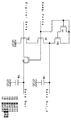
本発明の半導体装置の一例としてラッチ回路を図1に示し、その構成と動作について説明する。
【0046】
図1に示すラッチ回路は、TFT101〜105、および容量手段106、107を有する。TFT101、103、104のゲート電極には、シフトレジスタより出力されるサンプリングパルス(Samp.Pulse)が入力され、TFT102のゲート電極およびTFT104の入力電極には,デジタル映像信号(Digital Data)が入力される。TFT105の入力電極とゲート電極は、高電位側電源VDDに接続され、TFT105の出力電極とTFT101の出力電極は、TFT103の入力電極に接続され、TFT101の入力電極は、TFT102の出力電極に接続され、TFT102の入力電極は、低電位側電源VSSに接続されている。
【0047】
この構成の特徴としては、デジタル映像信号の入力に対し、出力(Data Out)、反転出力(Data Out_b)の2出力を得る点である。
【0048】
次いで、図1に示したラッチ回路の動作について説明する。なお、サンプリングパルスおよびデジタル映像信号の、入力時の振幅はいずれもVDD−VSS間とする。
【0049】
シフトレジスタより出力されたサンプリングパルスが、TFT101、103、104のゲート電極に入力され、TFT101、103、104がONする。入力されているデジタル映像信号がHi電位のとき、TFT102のゲート電極にHi電位が入力されてONする。
【0050】
このとき、TFT102、103がともにONし、貫通電流が流れる。TFT102およびTFT103の電流能力を、TFT105の電流能力よりも十分に高くしておくことにより、TFT101、105の出力電極、つまり反転出力端子(Data Out_b)にはLo電位が現れる。出力端子(Data Out)には、デジタル映像信号がTFT104を通じてそのままHi電位が出力される。
【0051】
一方、入力されているデジタル映像信号がLo電位のとき、TFT102のゲート電極にはLo電位が入力されてOFFする。よって、反転出力端子(Data Out_b)にはHi電位が現れる。出力端子(Data Out)には、デジタル映像信号がTFT104を通じてそのままLo電位が出力される。
【0052】
以上の動作が順次、1水平周期分行われる。出力端子(Data Out)および反転出力端子(Data Out_b)に出力された信号は、それぞれ容量手段106、107によって、帰線期間までの間、保持される。なお、後段の回路構成や、水平期間の長さによっては、容量手段106、107はなくてもよい。
【0053】
サンプリングパルス(Samp.Pulse)がLo電位となり、サンプリング期間が終了すると、TFT101、103、104がOFFする。つまり、反転出力端子(Data Out_b)および出力端子(Data Out)は浮遊状態となる。
【0054】
また、図1に示した本発明のラッチ回路においては、VDD−TFT101−TFT102−VSS間に電流パスが生ずるのは、サンプリングパルスが入力されており、かつデジタル映像信号がHi電位の時に限られる。
【0055】
ここで、出力端子(Data Out)側に現れる出力信号の振幅は、TFT101のしきい値の影響を受けるため、(VDD−VthN)−VSS間となる。また、反転出力端子(Data Out_b)側に現れる出力信号の振幅は、TFT102のしきい値の影響を受けるため、同様に(VDD−VthN)−VSS間となる。しかし、ラッチ回路の後段にバッファ回路を設けることにより、ブートストラップを用いて振幅の補償を行うため、問題とはならない。
【0056】
図1に示した回路において、TFT101とTFT102の位置を入れ替えても良い。また、図1に示した回路は、課題を解決するための手段で述べた本発明におけるラッチ回路の性質を全て満たす回路となっている。
【0057】
また、図1ではTFT101、102がNチャネル型の場合を示したが、本発明はこれに限定されない。電源電圧および入出力信号を反転することで、Pチャネル型のTFT101、102を用いることが出来る。
【0058】
【実施例】
(実施例1)
本実施例は、実施の形態とは異なる構成のラッチ回路について、図11を用いて説明する。
【0059】
図11は、図1に示した本発明のラッチ回路の接続に小変更を加えたものである。図11では、図1と対応する箇所には同じ番号を用いる。
【0060】
図1においては、TFT105のゲート電極と入力電極が接続されていたが、図11に示すラッチ回路では、TFT105のゲート電極と入力電極の間に新たにTFT111が設けられている。TFT111のゲート電極と入力電極とは電源VDDに接続されており、TFT111の出力電極はTFT105のゲート電極と接続されている。
【0061】
上記構成では、TFT105のゲート容量を用いたブートストラップによって、TFT105のゲート電極がVDDよりも電位が上昇する。つまり、図11に示したラッチ回路は、図1に示したラッチ回路と比較して、TFT105の電流能力が高く、反転出力端子(Data Out_b)の立ち上がりが早い。
【0062】
容量手段106、107は、後段の回路構成や水平期間の長さによってはなくてもよい。また、TFT101とTFT102の位置を入れ替えても良い。また、図11に示した回路は、課題を解決するための手段で述べた本発明におけるラッチ回路の性質を全て満たす回路となっている。
【0063】
なお、本実施例はTFTがNチャネル型の場合を示したが、TFTがPチャネル型の場合に対しても適用することが出来る。
【0064】
(実施例2)
本実施例は、実施の形態、実施例1とは異なる構成のラッチ回路について、図12を用いて説明する。
【0065】
図12は、図1に示した本発明のラッチ回路の接続に小変更を加えたものである。図12では、図1と対応する箇所には同じ番号を用いている。
【0066】
図1においては、TFT101の出力電極と電源VDDとの間にはダイオード接続されたTFT105が接続されていたが、図12に示すラッチ回路では、TFT101の出力電極と電源VDDとの間に、抵抗手段121が接続されている。
【0067】
容量手段106、107は、後段の回路構成や水平期間の長さによってはなくてもよい。また、TFT101とTFT102の位置を入れ替えても良い。また、図12に示した回路は、課題を解決するための手段で述べた本発明におけるラッチ回路の性質を全て満たす回路となっている。
【0068】
なお、本実施例はTFTがNチャネル型の場合を示したが、TFTがPチャネル型の場合に対しても適用することが出来る。
【0069】
(実施例3)
本実施例は、実施の形態、実施例1、2とは異なる構成のラッチ回路について、図13を用いて説明する。
【0070】
図13に示した本発明のラッチ回路は、TFT131〜134、および容量手段135、136を有する。TFT131、133、134のゲート電極には、シフトレジスタより出力されるサンプリングパルス(Samp.Pulse)が入力され、TFT132のゲート電極およびTFT134の入力電極には,デジタル映像信号(Digital Data)が入力される。
【0071】
TFT133の入力電極は高電位側電源VDDに接続され、TFT133の出力電極とTFT131の出力電極とは、反転出力端子(DATA Out_b)に出力される。TFT131の入力電極はTFT132の出力電極に接続され、TFT132の入力電極は低電位側電源VSSに接続されている。
【0072】
次いで、図13に示すラッチ回路の動作について、以下に説明する。なお、サンプリングパルスおよびデジタル映像信号の入力時の振幅はいずれもVDD−VSS間とする。
【0073】
シフトレジスタより出力されたサンプリングパルスが、TFT131、133、134のゲート電極に入力され、TFT131、133、134がONする。入力されているデジタル映像信号がHi電位のとき、TFT132のゲート電極にHi電位が入力されてONする。
【0074】
このとき、TFT131、132、133がともにONし、貫通電流が流れる。TFT131およびTFT132の電流能力を、TFT133の電流能力よりも十分に高くしておくことにより、TFT131、133の出力電極、つまり反転出力端子(Data Out_b)にはLo電位が現れる。出力端子(DataOut)には、デジタル映像信号がTFT134を通じてそのままHi電位が出力される。
【0075】
一方、入力されているデジタル映像信号がLo電位のとき、TFT132のゲート電極にはLo電位が入力されてOFFする。よって、反転出力端子(Data Out_b)にはHi電位が現れる。出力端子(Data Out)には、デジタル映像信号がTFT134を通じてそのままLo電位が出力される。
【0076】
以上の動作が順次、1水平周期分行われる。出力端子(Data Out)および反転出力端子(Data Out_b)に出力された信号は、それぞれ容量手段135、136によって、帰線期間までの間、保持される。なお、後段の回路構成や、水平期間の長さによっては、容量手段106、107はなくてもよい。
【0077】
サンプリングパルス(Samp.Pulse)がLo電位となり、サンプリング期間が終了すると、TFT131、133、134がOFFする。つまり、反転出力端子(Data Out_b)および出力端子(Data Out)は浮遊状態となる。
【0078】
また、図13に示した本発明のラッチ回路においては、VDD−TFT133−TFT131ーTFT132−VSS間に電流パスが生ずるのは、サンプリングパルスが入力されており、かつデジタル映像信号がHi電位の時に限られる。
【0079】
ここで、出力端子(Data Out)側に現れる出力信号の振幅は、TFT101のしきい値の影響を受けるため、(VDD−VthN)−VSS間となり、反転出力端子(Data Out_b)側に現れる出力信号の振幅は、TFT102のしきい値の影響を受けるため、同様に(VDD−VthN)−VSS間となるが、以後、ラッチ回路の後段にバッファ回路を設けることにより、ブートストラップを用いて振幅の補償を行うため、問題とはならない。
【0080】
なお、図13に示した回路において、TFT131とTFT132の位置を入れ替えても良い。また、図13に示した回路は、課題を解決するための手段で述べた本発明におけるラッチ回路の性質を全て満たす回路となっている。
【0081】
なお図13ではTFT131、132がNチャネル型の場合を示したが、本発明はこれに限定されない。電源電圧および入出力信号を反転することで、Pチャネル型のTFT131、132を用いることが出来る。
【0082】
(実施例4)
本実施例は、実施の形態、実施例1乃至実施例3とは異なる構成のラッチ回路について、図30を用いて説明する。
【0083】
図30に示すラッチ回路は、図13に示した本発明のラッチ回路の接続に小変更を加えたものである。図13においては、TFT133の入力電極は電源VDDに接続されていたが、図30に示すラッチ回路では、TFT133の入力電極はサンプリングパルスに接続されている。
【0084】
なお図30に示すラッチ回路の動作は、実施例3で説明した図13に示すラッチ回路と同様であるので、本実施例では説明は省略する。
【0085】
容量手段135、136は、後段の回路構成や水平期間の長さによってはなくてもよい。また、TFT131とTFT132の位置を入れ替えても良い。また、図30に示した回路は、課題を解決するための手段で述べた本発明におけるラッチ回路の性質を全て満たす回路となっている。
【0086】
なお、本実施例はTFTがNチャネル型の場合を示したが、TFTがPチャネル型の場合に対しても適用することが出来る。
【0087】
(実施例5)
本実施例は、実施の形態、実施例1乃至実施例4とは異なる構成のラッチ回路について、図31を用いて説明する。
【0088】
図31に示すラッチ回路は、図13に示した本発明のラッチ回路の接続に小変更を加えたものである。図13においては、TFT133の入力電極は電源VDDに接続されていたが、図31に示すラッチ回路では、TFT133の入力電極はサンプリングパルスに接続されている。さらに、本発明のラッチ回路には、TFT141が設けられており、TFT141のゲート電極と入力電極にはサンプリングパルスが接続されており、TFT141の出力電極にはTFT133のゲート電極が接続されている。
【0089】
なお図31に示すラッチ回路の動作は、実施例3で説明した図13に示すラッチ回路と同様であるので、本実施例では説明は省略する。
【0090】
なお、容量手段135、136は、後段の回路構成や水平期間の長さによってはなくてもよい。また、TFT131とTFT132の位置を入れ替えても良い。
また、図30に示した回路は、課題を解決するための手段で述べた本発明におけるラッチ回路の性質を全て満たす回路となっている。
【0091】
なお、本実施例はTFTがNチャネル型の場合を示したが、TFTがPチャネル型の場合に対しても適用することが出来る。
【0092】
(実施例6)
本実施例は、実施の形態、実施例1乃至実施例5とは異なる構成のラッチ回路の構成とその動作について、図14を用いて説明する。
【0093】
図14は、実施の形態にて説明した構成でなる回路を第1のラッチ回路とし、第2のラッチ回路およびバッファまでを構成した例である。第1のラッチ回路1101は、TFT1111〜1115および容量手段1116、1117とを有し、第2のラッチ回路1102は、TFT1118、1119および容量手段1120、1121とを有し、バッファ回路1103は、TFT1122〜1125および容量手段1126でなるインバータと、TFT1127〜1130および容量手段1131でなるインバータとを有する。
【0094】
1水平周期分のサンプリングが終了した後の帰線期間中に、ラッチパルス(Latch Pulse)が入力されると、第2のラッチ回路1102におけるTFT1118、1119がONし、第1のラッチ回路1101において、容量手段1116、1117にて保持されている信号が、第2のラッチ回路1102における容量手段1120、1121に書き込まれる。
【0095】
サンプリングパルス(Samp.Pulse)がLo電位となり、サンプリング期間が終了すると、TFT1111、1113、1114がOFFする。よって、TFT1118、1119の入力電極は浮遊状態となる。続いて、ラッチパルス(Latch Pulse)が入力されると、TFT1118、1119がONし、容量手段1120、1121に信号が書き込まれるが、このとき、TFT1118、1119の入力電極に電流の供給源が接続されていないため、前述の動作は、容量手段1116、1117、1120、1121における電荷の移動のみによって行われることになる。よって容量手段1120、1121への書き込みが十分に行われるようにするためには、容量手段1116、1117は大きく設計しておくのが望ましい。
【0096】
続いて、第2のラッチ回路1102からの出力信号は、バッファ回路1103へと入力される。バッファ回路1103は、2つのインバータを対に配置したものであるので、ここでは、TFT1122〜1125および容量手段1126で構成されたインバータ一方のみの動作について述べる。
【0097】
第2のラッチ回路1102の一方の出力(Data Out2)がHi電位のとき、TFT1122のゲート電極にHi電位が入力されてONする。一方、TFT1123、1125のゲート電極には、第2のラッチ回路1102の他方の出力(Data Out2_b)であるLo電位が入力されてOFFする。よって、TFT1124のゲート電極の電位が上昇する。
【0098】
このとき、TFT1122のゲート電極の電位は、(VDD−VthN)であるので、TFT1124のゲート電極の電位が(VDD−2×VthN)となったところで、TFT1122のゲート・ソース間電圧がそのしきい値を下回り、OFFする。よってTFT1124のゲート電極は、その時点で一時浮遊状態となる。
【0099】
ここで、VthN<(VDD−VthN)であるならば、TFT1124がONし、バッファ1103の出力端子(Data Out3)にはHi電位が現れるので、電位が上昇する。さらに、TFT1124のゲート電極と出力電極との間には容量手段1126を有し、今、TFT1124のゲート電極は浮遊状態であるので、出力端子(Data Out3)の電位上昇に伴い、容量結合によってTFT1124のゲート電極の電位がさらに上昇する。
【0100】
その結果、TFT1124のゲート電極の電位が、(VDD+VthN)よりも高くなると、出力端子にHi電位が現れ、その電位はTFT1124のしきい値の影響を受けることなく、VDDに等しくなる。
【0101】
一方、第2のラッチ回路1102の一方の出力(Data Out2)がLo電位のとき、TFT1122のゲート電極にはLo電位が入力されてOFFする。一方、TFT1123、1125のゲート電極には、第2のラッチ回路1102の他方の出力(Data Out2_b)であるHi電位が入力されてONする。よってTFT1124のゲート電極の電位はLo電位となってOFFし、出力端子(Data Out3)にはLo電位が現れる。
【0102】
TFT1127〜1130および容量手段1131でなるインバータについても動作は同様であり、一方の出力端子(Data Out3)にHi電位が現れるときは、他方の出力端子(Data Out3_b)にはLo電位が現れる。
【0103】
本実施例で示したラッチ回路においては、第1のラッチ回路〜第2のラッチ回路において、TFTのしきい値分の振幅減衰が生ずるため、電源電圧がある程度高い必要がある。そこで、第1のラッチ回路の出力を、一旦バッファを介して振幅の補償を行う構成としても良い。
【0104】
なお、本実施例において、容量手段1120、1121はなくともよい。容量手段1120、1121によって保持される情報は、ラッチパルス(LatchPulse)により、TFT1118、1119がONすると、そのままバッファ回路1103の出力端子(Data Out3およびData Out3_b)に伝達される。バッファ回路1103の出力電位は、ブートストラップに用いられる容量手段1126、1131によって保持されるため、これを用いてデータをラッチしても良い。
【0105】
なお、本実施例はTFTがNチャネル型の場合を示したが、TFTがPチャネル型の場合に対しても適用することが出来る。
【0106】
本実施例は実施の形態、実施例1乃至実施例5と自由に組み合わせて実施することが可能である。
【0107】
(実施例7)
前述した実施例6においては、第1のラッチ回路からの出力は、直ちに第2のラッチ回路に入力され、振幅減衰の補償は、第2のラッチ回路の後段に配置されたバッファ回路が行っている。但しこの場合、動作電圧が低く、かつTFTのしきい値が大きい場合、元の振幅に対してしきい値分の減衰による影響が大きく、ラッチ回路において正常な保持動作が行われないことが考えられる。
【0108】
そこで本実施例では、第1のラッチ回路の後段に振幅補償用バッファ回路を追加した構成をする構成の半導体装置について説明する。
【0109】
図32に本発明の半導体装置の構成を示す。点線枠1201で囲まれた部分は、実施の形態で説明した第1のラッチ回路であり、TFT1211〜1215、および容量手段1216、1217を有している。
【0110】
点線枠1202で囲まれた部分が、第1のラッチ回路からの出力振幅を補償するための、振幅補償用バッファ回路であり、TFT1218〜1222、および容量手段1220、1223を有している。
【0111】
次いで、図32に示した半導体装置の動作について説明する。ここで、TFT1218、1219および容量手段1220で構成される回路と、TFT1221、1222および容量手段1223で構成される回路とは、入力される信号の極性が逆であることを除いて、上述した実施例で説明した動作と同様の動作をする。そのため本実施例では、TFT1218、1219および容量1220で構成される回路のみの動作について説明する。
【0112】
第1のラッチ回路1201に、サンプリングパルス(Samp.Pulse)とデジタル映像信号(Digital Data)とが入力され、第1の出力信号(Data Out)および第2の出力信号(Data Out_b)が出力される。
【0113】
TFT1214の出力電極から出力される信号を第1の出力信号、TFT1213の出力電極から出力される信号を第2の出力信号とする。第2の出力信号は、第1の出力信号に対して反転した極性を有する。
【0114】
第1のラッチ回路に入力されるデジタル映像信号(Digital Data)がHi電位のとき、第1の出力信号はHi電位、第2の出力信号はLo電位であり、第1のラッチ回路に入力されるデジタル映像信号(Digital Data)がLo電位のとき、第1の出力信号はLo電位、第2の出力信号はHi電位である。
【0115】
ここで、第1および第2の出力信号の振幅は、第1のラッチ回路にてTFT1213、1214のしきい値の影響を受けるため、(VDD−VthN)−VSS間となっている。つまりVthNだけ、振幅の減衰を生じている。
【0116】
第1の出力信号がLo電位、第2の出力信号がHi電位である場合、TFT1218のゲート電極にはHi電位が入力され、TFT1219のゲート電極にはLo電位が入力される。
【0117】
一方、第1のラッチ回路でサンプリング期間が終了すると、サンプリングパルスはLo電位となり、TFT1214、1213がOFFする。よって、TFT1218、1219のゲート電極は、その瞬間の電位を容量手段1216、1214によって保持されつつ、浮遊状態となる。
【0118】
このときのTFT1218のゲート電極の電位はHi電位、すなわち(VDD−VthN)であり、TFT1219のゲート電極の電位はVSSである。よって、TFT1218はONし、TFT1218の出力電極の電位が上昇する。このとき、TFT1219はOFFする。
【0119】
ここで、容量手段1220による、TFT1218のゲート電極と出力電極間の容量結合によってブートストラップが働き、TFT1218のゲート電極の電位は(VDD−VthN)からさらに上昇して、(VDD+VthN)よりも高い電位をとる。よって、TFT1218の出力電極の電位、すなわちバッファ出力(Data Out')の電位は、VDDに等しくなる。
【0120】
一方、TFT1218のゲート電極にLo電位が入力され、TFT1218のゲート電極にHi電位が入力されると、バッファ出力はLo電位となる。
【0121】
以上の動作が、TFT1221、1222および容量手段1223によって構成される回路においても同様になされ、バッファ出力がHi電位のとき、反転バッファ出力(Data Out_b')はLo電位となり、バッファ出力がLo電位のとき、反転バッファ出力はHi電位となる。
【0122】
よって、第1のラッチ回路の出力の振幅が補償され、正常にVDD−VSS間の振幅が得られ、第2のラッチ回路へと入力することが出来る。
【0123】
ここで、TFT1218のゲート電極と出力電極間にブートストラップが働くとき、同時にTFT1219のゲート電極も浮遊状態となっているため、特に容量手段を設けない場合にも、TFT1219それ自身のゲート・ドレイン間容量によって、TFT1219のゲート電極の電位が上昇する可能性がある。これによって、TFT1219がONすると、誤動作を招くため、TFT1219のゲート・ドレイン間につく容量は小さくする、すなわちTFT1219のサイズをTFT1218よりも小さくする等の対策があると望ましい。
【0124】
図32において、容量手段1216、1217の容量は小さい方が好ましい。これは、容量手段1216、1217の容量が大きいと、ブートストラップによるTFT1218、1221のゲート電極の上昇幅が小さくなってしまうためである。特に、容量手段1216、1217は設けなくても良い。その場合も、バッファ出力(Data Out)および反転バッファ出力(Data Out_b)の電位は、容量手段1220および1223によって、それぞれ保持されるので問題はない。
【0125】
なお、本実施例はTFTがNチャネル型の場合を示したが、TFTがPチャネル型の場合に対しても適用することが出来る。
【0126】
本実施例は実施の形態、実施例1乃至実施例6と自由に組み合わせて実施することが可能である。
【0127】
(実施例8)
本実施例においては、同一基板上に画素部および画素部周辺に設ける駆動回路のTFTを同じに作製する方法について説明する。なお、例として液晶表示回路の作製工程を挙げるが、もちろん本発明は液晶表示装置に限定されるものではない。
【0128】
まず、図7(A)に示すように、コーニング社の#7059ガラスや#1737ガラスなどに代表されるバリウムホウケイ酸ガラス、またはアルミノホウケイ酸ガラスなどのガラス、耐熱性プラスチックから成る基板3001上に酸化シリコン膜、窒化シリコン膜、または酸化窒化シリコン膜などの絶縁膜から成る下地膜3002を形成する。例えば、プラズマCVD法でSiH4、NH3、N2Oから作製される酸化窒化シリコン膜3002aを10〜200[nm](好ましくは50〜100[nm])形成し、同様にSiH4、N2Oから作製される酸化窒化水素化シリコン膜3002bを50〜200[nm](好ましくは100〜150[nm])の厚さに積層形成する。本実施例では下地膜3002を2層構造として示したが、前記絶縁膜の単層膜または2層以上積層させた構造として形成しても良い。
【0129】
島状半導体層3003〜3005は、非晶質構造を有する半導体膜をレーザー結晶化法や公知の熱結晶化法を用いて作製した結晶質半導体膜で形成する。この島状半導体層3003〜3005の厚さは25〜80[nm](好ましくは30〜60[nm])の厚さで形成する。結晶質半導体膜の材料に限定はないが、好ましくはシリコンまたはシリコンゲルマニウム(SiGe)合金などで形成すると良い。
【0130】
レーザー結晶化法で結晶質半導体膜を作製するには、パルス発振型または連続発光型のエキシマレーザーやYAGレーザー、YVO4レーザーを用いる。これらのレーザーを用いる場合には、レーザー発振器から放射されたレーザー光を光学系で線状に集光し半導体膜に照射する方法を用いると良い。結晶化の条件は実施者が適宣選択するものであるが、エキシマレーザーを用いる場合はパルス発振周波数30[Hz]とし、レーザーエネルギー密度を100〜400[mJ/cm2](代表的には200〜300[mJ/cm2])とする。また、YAGレーザーを用いる場合にはその第2高調波を用いパルス発振周波数1〜10[kHz]とし、レーザーエネルギー密度を300〜600[mJ/cm2](代表的には350〜500[mJ/cm2])とすると良い。そして幅100〜1000[μm]、例えば400[μm]で線状に集光したレーザー光を基板全面に渡って照射し、この時の線状レーザー光の重ね合わせ率(オーバーラップ率)を80〜98[%]として行う。
【0131】
次いで、島状半導体層3003〜3005を覆うゲート絶縁膜3006を形成する。ゲート絶縁膜3006はプラズマCVD法またはスパッタ法を用い、厚さを40〜150[nm]としてシリコンを含む絶縁膜で形成する。本実施例では、120[nm]の厚さで酸化窒化シリコン膜で形成する。勿論、ゲート絶縁膜はこのような酸化窒化シリコン膜に限定されるものでなく、他のシリコンを含む絶縁膜を単層または積層構造として用いても良い。例えば、酸化シリコン膜を用いる場合には、プラズマCVD法でTEOS(Tetraethyl Orthosilicate)とO2とを混合し、反応圧力40[Pa]、基板温度300〜400[℃]とし、高周波(13.56[MHz])、電力密度0.5〜0.8[W/cm2]で放電させて形成することが出来る。このようにして作製される酸化シリコン膜は、その後400〜500[℃]の熱アニールによりゲート絶縁膜として良好な特性を得ることが出来る。
【0132】
そして、ゲート絶縁膜3006上にゲート電極を形成するための第1の導電膜3007と第2の導電膜3008とを形成する。本実施例では、第1の導電膜3007をTaで50〜100[nm]の厚さに形成し、第2の導電膜3008をWで100〜300[nm]の厚さに形成する。
【0133】
Ta膜はスパッタ法で、TaのターゲットをArでスパッタすることにより形成する。この場合、Arに適量のXeやKrを加えると、Ta膜の内部応力を緩和して膜の剥離を防止することが出来る。また、α相のTa膜の抵抗率は20[μΩcm]程度でありゲート電極に使用することが出来るが、β相のTa膜の抵抗率は180[μΩcm]程度でありゲート電極とするには不向きである。α相のTa膜を形成するために、Taのα相に近い結晶構造をもつ窒化タンタル(TaN)を10〜50[nm]程度の厚さでTaの下地に形成しておくとα相のTa膜を容易に得ることが出来る。
【0134】
W膜を形成する場合には、Wをターゲットとしたスパッタ法で形成する。その他に6フッ化タングステン(WF6)を用いる熱CVD法で形成することも出来る。いずれにしてもゲート電極として使用するためには低抵抗化を図る必要があり、W膜の抵抗率は20[μΩcm]以下にすることが望ましい。W膜は結晶粒を大きくすることで低抵抗率化を図ることが出来るが、W中に酸素などの不純物元素が多い場合には結晶化が阻害され高抵抗化する。このことより、スパッタ法による場合、純度99.9999[%]のWターゲットを用い、さらに成膜時に気相中からの不純物の混入がないように十分配慮してW膜を形成することにより、抵抗率9〜20[μΩcm]を実現することが出来る。
【0135】
なお、本実施例では、第1の導電膜3008をTa、第2の導電膜3009をWとしたが、特に限定されず、いずれもTa、W、Ti、Mo、Al、Cuなどから選ばれた元素、または前記元素を主成分とする合金材料もしくは化合物材料で形成しても良い。また、リン等の不純物元素をドーピングした多結晶シリコン膜に代表される半導体膜を用いても良い。本実施例以外の組み合わせの一例で望ましいものとしては、第1の導電膜3007を窒化タンタル(TaN)で形成し、第2の導電膜3008をWとする組み合わせ、第1の導電膜3007を窒化タンタル(TaN)で形成し、第2の導電膜3008をAlとする組み合わせ、第1の導電膜3007を窒化タンタル(TaN)で形成し、第2の導電膜3008をCuとする組み合わせ等が挙げられる。
【0136】
次に、レジストによるマスク3009〜3012を形成し、電極及び配線を形成するための第1のエッチング処理を行う。本実施例ではICP(Inductively Coupled Plasma:誘導結合型プラズマ)エッチング法を用い、エッチング用ガスにCF4とCl2を混合し、1[Pa]の圧力でコイル型の電極に500[W]のRF(13.56[MHz])電力を投入してプラズマを生成して行う。基板側(試料ステージ)にも100[W]のRF(13.56[MHz])電力を投入し、実質的に負の自己バイアス電圧を印加する。CF4とCl2を混合した場合にはW膜及びTa膜とも同程度にエッチングされる。
【0137】
上記エッチング条件では、レジストによるマスクの形状を適したものとすることにより、基板側に印加するバイアス電圧の効果により第1の導電層及び第2の導電層の端部がテーパー形状となる。テーパー部の角度は15〜45°となる。ゲート絶縁膜上に残渣を残すことなくエッチングするためには、10〜20[%]程度の割合でエッチング時間を増加させると良い。W膜に対する酸化窒化シリコン膜の選択比は2〜4(代表的には3)であるので、オーバーエッチング処理により、酸化窒化シリコン膜が露出した面は20〜50[nm]程度エッチングされることになる。こうして、第1のエッチング処理により第1の導電層と第2の導電層から成る第1の形状の導電層3013〜3016(第1の導電層3013a〜3016aと第2の導電層3013b〜3016b)を形成する。このとき、ゲート絶縁膜3006においては、第1の形状の導電層3013〜3016で覆われない領域は20〜50[nm]程度エッチングされ薄くなった領域3017が形成される。(図7(B))
【0138】
続いて、図7(C)に示すように、レジストマスク3009〜3012は除去しないまま、第2のエッチング処理を行う。エッチングガスにCF4とCl2とO2とを用い、W膜を選択的にエッチングする。この時、第2のエッチング処理により第2の形状の導電層3018〜3021(第1の導電層3018a〜3021aと第2の導電層3018b〜3021b)を形成する。このとき、ゲート絶縁膜3006においては、第2の形状の導電層3018〜3021で覆われない領域はさらに20〜50[nm]程度エッチングされ薄くなった領域3022が形成される。
【0139】
W膜やTa膜のCF4とCl2の混合ガスによるエッチング反応は、生成されるラジカルまたはイオン種と反応生成物の蒸気圧から推測することが出来る。WとTaのフッ化物と塩化物の蒸気圧を比較すると、Wのフッ化物であるWF6が極端に高く、その他のWCl5、TaF5、TaCl5は同程度である。従って、CF4とCl2の混合ガスではW膜及びTa膜共にエッチングされる。しかし、この混合ガスに適量のO2を添加するとCF4とO2が反応してCOとFになり、FラジカルまたはFイオンが多量に発生する。その結果、フッ化物の蒸気圧が高いW膜のエッチング速度が増大する。一方、TaはFが増大しても相対的にエッチング速度の増加は少ない。また、TaはWに比較して酸化されやすいので、O2を添加することでTaの表面が酸化される。Taの酸化物はフッ素や塩素と反応しないためさらにTa膜のエッチング速度は低下する。従って、W膜とTa膜とのエッチング速度に差を作ることが可能となりW膜のエッチング速度をTa膜よりも大きくすることが可能となる。
【0140】
そして、第1のドーピング処理を行いn型を付与する不純物元素を添加する。ドーピングの方法はイオンドープ法もしくはイオン注入法で行えば良い。イオンドープ法の条件はドーズ量を1×10¹³〜5×10¹⁴[atoms/cm2]とし、加速電圧を60〜100[keV]として行う。n型を付与する不純物元素として15族に属する元素、典型的にはリン(P)または砒素(As)を用いるが、ここではリン(P)を用いる。この場合、導電層3018〜3021がn型を付与する不純物元素に対するマスクとなり、自己整合的に第1の不純物領域3023〜3025が形成される。第1の不純物領域3023〜3025には1×1020〜1×1021[atoms/cm3]の濃度範囲でn型を付与する不純物元素を添加する。(図7(C))
【0141】
そして、図7(D)に示すように画素部TFTになる部分をレジストマスク3026で覆った上での第2のドーピング処理を行う。このとき、画素部TFTは全てレジストマスクで覆わずに外側を開けてドーピングを行う。第2のドーピング処理は、第1のドーピング処理よりもドーズ量を下げて高い加速電圧の条件としてn型を付与する不純物元素をドーピングする。例えば、加速電圧を70〜120[keV]とし、1×10¹³[atoms/cm2]のドーズ量で行い、図7(D)で島状半導体層に形成された第1の不純物領域3023〜3025内に新たな不純物領域3017〜3029を形成する。ドーピングは、第2の形状の導電層3018、3019を不純物元素に対するマスクとして用い、レジストマスクで覆われていないところの第1の導電層3018a、3019aの下側の領域の半導体層にも不純物元素が添加されるようにドーピングする。こうして、第3の不純物領域3030、3031が形成される。この第3の不純物領域3030、3031に添加されたリン(P)の濃度は、第1の導電層3018a、3019aのテーパー部の膜厚に従って緩やかな濃度勾配を有している。なお、第1の導電層3018a、3019aのテーパー部と重なる半導体層において、第1の導電層3018a、3019aのテーパー部の端部から内側に向かって若干、不純物濃度が低くなっているものの、ほぼ同程度の濃度である。
【0142】
以上までの工程でそれぞれの島状半導体層に不純物領域が形成される。島状半導体層と重なる第3の形状の導電層3018〜3021がゲート電極として機能する。
【0143】
レジストマスク3026を除去した後、導電型の制御を目的として、それぞれの島状半導体層に添加された不純物元素を活性化する工程を行う。この工程はファーネスアニール炉を用いる熱アニール法で行う。その他に、レーザーアニール法、またはラピッドサーマルアニール法(RTA法)を適用することが出来る。熱アニール法では酸素濃度が1[ppm]以下、好ましくは0.1[ppm]以下の窒素雰囲気中で400〜700[℃]、代表的には500〜600[℃]で行うものであり、本実施例では500[℃]で4時間の熱処理を行う。ただし、第3の形状の導電層3018〜3021に用いた配線材料が熱に弱い場合には、配線等を保護するため層間絶縁膜3032(シリコンを主成分とする)を形成した後で活性化を行うことが好ましい(図8(A))。
【0144】
さらに、3〜100[%]の水素を含む雰囲気中で、300〜450[℃]で1〜12時間の熱処理を行い、島状半導体層を水素化する工程を行う。この工程は熱的に励起された水素により半導体層のダングリングボンドを終端する工程である。水素化の他の手段として、プラズマ水素化(プラズマにより励起された水素を用いる)を行っても良い(図8(A))。
【0145】
次いで、図8(B)のように第1の層間絶縁膜3032は酸化窒化シリコン膜から100〜200[nm]の厚さで形成する。その上にアクリルなどの有機絶縁物材料から成る第2の層間絶縁膜3033を形成する。本実施例ではTFTによって形成される段差を十分に平坦化しうる膜厚で形成する。好ましくは1〜5[μm](さらに好ましくは2〜4[μm])とすれば良い。
【0146】
また、第2の層間絶縁膜3033として有機絶縁物材料の代わりに無機材料を用いることもできる。無機材料としては無機SiO2やプラズマCVD法で作製したSiO2(PCVD‐SiO2)、SOG(Spin on Glass;塗布珪素酸化膜)等が用いられる。
【0147】
2つの層間絶縁膜を形成した後にコンタクトホールを形成するためのエッチング工程を行う。ドライエッチングまたはウェットエッチング法を用い、N型の不純物領域3027〜3029、およびソース信号線(図示せず)、およびゲート信号線(図示せず)、電流供給線(図示せず)、およびゲート電極3018〜3021に達する(図示せず)コンタクトホールをそれぞれ形成する。
【0148】
また、配線3034〜3037として、Ti膜を100[nm]、Tiを含むAl膜を300[nm]、Ti膜を150[nm]、スパッタ法で連続形成した3層積層の膜を所望の形状にパターンニングして形成する。勿論、他の導電性材料を用いても良い。画素電極3038については、表示装置を反射方とする場合には、反射性の高い材料にて形成する。この場合、配線と同じに形成しても良い。一方、透過型である場合には、酸化インジウム錫(Indium Tin Oxside:ITO)等の透明導電膜材料を用いて形成する。図8(B)の状態まで完了したものを、本明細書ではアクティブマトリクス基板と呼ぶ。
【0149】
続いて、対向基板3039を用意する。対向基板3039には、遮光膜3041が形成される。この遮光膜は、クロム(Cr)などを用いて、100[nm]〜200[nm]の厚さで形成する。
【0150】
一方、画素部においては図8(C)のように対向電極3041が形成される。対向電極は、ITOの透明導電性材料を用いて形成する。また、可視光の透過率を高く保つために対向電極の膜厚は100[nm]〜120[nm]で形成することが望ましい。
【0151】
アクティブマトリクス基板と対向基板とに、配向膜3042、3043を形成する。配向膜3042、3043の膜厚は、30[nm]〜80[nm]が望ましい。また、配向膜としては、例えば日産化学社製SE7792などを用いることができる。プレチルト角の高い配向膜を用いると、アクティブマトリクス方式により駆動される液晶表示装置の駆動時にディスクリネーションの発生を抑制することができる。
【0152】
続いて、配向膜3042、3043をラビングする。ラビング方向は、液晶表示装置が完成したときに、左巻きのTN(Twisted Nematic)配向となるようにするのが望ましい。
【0153】
本実施例においては特に図示しないが、スペーサを画素内に散布もしくはパターンニングにより形成して、セルギャップの均一性を向上させることも可能である。本実施例においては、感光性樹脂膜を製膜、パターンニングして4.0[μm]の高さのスペーサを形成した。
【0154】
続いて、シール剤3044により、アクティブマトリクス基板と対向基板とを貼り合わせる。シール剤としては、熱硬化型のシール剤である三井化学社製XN−21Sを用いた。シール剤中にはフィラーを混入する。なお、フィラーの高さは4.0[μm]とする。その後、シール剤が硬化した後に、アクティブマトリクス基板と対向基板とを、所望のサイズに同時に分断する。
【0155】
続いて、液晶材料3045を注入する。液晶材料としては、高速応答特性を考慮すると、低粘度のものが望ましい。本実施例においては、配向制御の容易なネマチック液晶を用いる。勿論、高速応答な可能な強誘電性液晶、反強誘電性液晶を用いても良い。
【0156】
液晶材料の注入が終了したのち、注入口をUV硬化型樹脂等を用いて封止する。その後、公知の方法により偏光板を貼り付ける。最後に、基板上に形成された素子は回路から引き回された端子と外部信号端子とを接続するためのコネクタ(フレキシブルプリントサーキット:FPC)を取り付けて製品として完成する(図8(C))。このような出荷できる常態までにした状態を本明細書中では液晶表示装置と呼ぶ。
【0157】
また、本明細書中で示す工程に従えば、アクティブマトリクス基板の作製に必要なフォトマスクの数を5枚(島状半導体層パターン、第1配線パターン(ソース信号線、容量配線)、マスクパターン、コンタクトホールパターン、第2配線パターン(画素電極、接続電極含む))とすることができる。その結果、工程を短縮し、製造コストの低減及び歩留まりの向上に寄与することができる。
【0158】
実施例ではNMOS構成のTFTを示したが、このようなTFTを使って図1で示すようなラッチ回路を形成することができる。
【0159】
なお、本実施例では、書き込み用TFTは、ダブルゲート構造で示したが、シングルゲート構造やトリプルゲート構造でも構わないし、マルチゲート構造でも構わない。
【0160】
なお、本実施例においては、TFTの型式としてはトップゲート型TFTを例に挙げて説明しているが、その他に、図26(A)に示すような活性層の下側にゲート電極を形成したボトムゲート型TFT、あるいは図26(B)に示すような、活性層を挟み込むように、上下にゲート電極を有するデュアルゲート型TFTを用いても実施が可能である。
【0161】
本実施例は、実施の形態、実施例1乃至実施例7と自由に組み合わせて実施することが可能である。
【0162】
(実施例9)
本実施例においては、実施の形態に示した回路、実施例1乃至実施例7に示した回路、実施例8で示したTFTの作製工程を参考にして、TFTを作製し実際に表示装置(半導体装置)を作成した例について述べる。
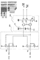
【0163】
図2(A)に表示装置の概略図を示す。基板200の中央部に、画素部201が配置されている。画素部201の周辺には、ソース信号線を制御するための、ソース信号線駆動回路202および、ゲート信号線を制御するための、ゲート信号線駆動回路207が配置されている。ゲート信号線駆動回路207は、図2(A)では画素部201の両側に対称配置されているが、画素部201の片側のみに配置しても良い。
【0164】
ソース信号線駆動回路202、ゲート信号線駆動回路207を駆動するために外部より入力される信号は、FPC210を介して入力される。本実施例においては、FPC210より入力される信号は、その電圧振幅が小さいため、本実施例では、レベルシフタ206によって電圧振幅の変換を受けた上で、ソース信号駆動回路202、およびゲート信号線駆動回路207へと入力される。
【0165】
図2(A)において、破線A−A’の断面図を図2(B)に示す。基板200上には、画素部201、ソース信号線駆動回路202、ゲート信号線駆動回路(図示せず)が形成されている。基板200と対向基板211とは、シール剤212を用いて貼り合わされ、基板間のギャップには液晶が注入される。液晶の注入後は、図2(A)に示すように、封止剤213によって、注入口を密閉する。
【0166】
引きまわし配線221は、異方導電性フィルム223を介して、FPC210が有するFPC側配線222と電気的に接続される。異方導電性フィルム223には、図2(C)に示すような導電性のフィラー224が含まれており、基板200とFPC210とを熱圧着することで、基板200の引きまわし配線221と、FPC210上のFPC側配線222とが、導電性フィラー224によって電気的に接続される。
【0167】
ソース信号線駆動回路202の構成を図3に示す。点線枠300で示されるシフトレジスタは、クロック信号とスタートパルスとに従ってサンプリングパルスを出力するパルス出力回路301を複数段用いて構成される。第1のラッチ回路302〜第2のラッチ回路303〜バッファ回路304は、実施例1にて図11に示したものを用いている。図3のソース信号線駆動回路には、3ビットのデジタル映像信号(DATA1〜DATA3)が入力される。よって、第1のラッチ回路302〜第2のラッチ回路303〜バッファ回路304は、3組が並列に配置され、1つのパルス出力回路301から出力されるサンプリングパルスによって、同時に3ビットずつのデジタル映像信号の保持を行う。
【0168】
D/A変換回路305に関しては、本明細書中では特に図示していないが、従来用いられている抵抗分割型、容量型など、いずれの形式のものを用いても良い。
【0169】
D/A変換回路305にて、3ビットのデジタル映像信号は8階調のアナログ映像信号へと変換され、それぞれ、ソース信号線(S0001〜S最終)へと書き込まれる。
【0170】
なお、外部より入力される信号は、IC等の集積回路より出力されるため、近年の低電圧化に伴い、3[V]〜5[V]程度の低電圧振幅の信号である場合が多いため、それぞれのレベルシフタ306〜309によって、高電圧振幅への信号へと変換されたあと、駆動回路へと入力される。
【0171】
ゲート信号線駆動回路207の構成を図4に示す。点線枠400に示されるシフトレジスタは、クロック信号とスタートパルスとに従ってゲート信号線選択パルスを選択するパルス出力回路401を複数段用いて構成される。ゲート信号線の負荷が大きい場合には、すなわち、シフトレジスタより出力されるゲート信号線選択パルスが、直接ゲート信号線の電位をHi電位、Lo電位と切り替えるだけの駆動能力を有していない場合、バッファ404を用いる必要がある。
【0172】
なお、外部より入力される信号は、IC等の集積回路より出力されるため、近年の低電圧化に伴い、3[V]〜5[V]程度の低電圧振幅の信号である場合が多いため、それぞれのレベルシフタ401、402によって、高電圧振幅への信号へと変換されたあと、駆動回路へと入力される。
【0173】
本実施例は、実施の形態、実施例1乃至実施例7と自由に組み合わせて実施することが可能である。
【0174】
(実施例10)
実施例8に示した工程は、画素および周辺の駆動回路はNチャネル型TFTを用いて構成する場合の例として説明したが、本発明はPチャネル型TFTを用いて作製することも出来る。
【0175】
Nチャネル型TFTの場合、ホットキャリア劣化等の抑制のため、ゲート電極と重なる領域に、オーバーラップ領域と呼ばれる不純物領域を設けている。これに対してPチャネル型TFTの場合は、ホットキャリア劣化による影響が小さいので、特にオーバーラップ領域を設ける必要はなく、この場合より簡単な工程で作成することが可能である。
【0176】
図9(A)に示すように、実施例8に従って、ガラスや耐熱性プラスチックなどを用いた絶縁基板3101上に下地膜3102を形成し、次いで島状の半導体層3103〜3105、ゲート絶縁膜3106、導電層3107、3108を形成する。ここで、導電層3107、3108はここでは積層構造としているが、特に単層であってもかまわない。
【0177】
次いで、図9(B)に示すように、レジストによるマスク3109〜3112を形成し、第1のエッチング処理を行う。実施例8においては、積層構造とした導電層の材質による選択比を利用して、異方性エッチングを行ったが、ここでは特にオーバーラップ領域となる領域を設ける必要はないので、通常エッチングにて行えば良い。このとき、ゲート絶縁膜3106においては、エッチングによって20[nm]〜50[nm]程度薄くなった領域3117が形成される。
【0178】
続いて、図9(C)に示すように、島状の半導体層にP型を付与する不純物元素を添加するために第1のドーピング処理を行う。導電層3113〜3116を不純物元素に対するマスクとして用い、自己整合的に不純物領域を形成する。P型を付与する不純物元素としては、ボロン(B)等が代表的である。ここでは、ジボラン(B2H6)を用いたイオンドープ法で形成し、半導体中の不純物濃度が2×10²⁰〜2×10²¹[atoms/cm3]となるようにする。
【0179】
レジストとなるマスクを除去して、図9(D)の状態を得る。以後、実施例8における図8(B)以降の工程に従って作製する。
【0180】
本実施例は、実施の形態、実施例1乃至実施例7、実施例9と自由に組み合わせて実施することが可能である。
【0181】
(実施例11)
本実施例は、本発明の半導体装置が有するTFTの半導体活性層を作製する上で、半導体膜を結晶化する手法の例を示す。
【0182】
ガラス基板上に下地膜として、プラズマCVD法により酸化窒化珪素膜(組成比Si=32%、O=59%、N=7%、H=2%)400nmを形成した。続いて、前記下地膜上に半導体膜として、プラズマCVD法により非晶質珪素膜150nmを形成した。そして、500℃で3時間の熱処理を行って、半導体膜が含有する水素を放出させた後、レーザアニール法により半導体膜の結晶化を行った。
【0183】
レーザアニ-ル法に用いるレーザとしては、連続発振のYVO4レーザを用いた。レーザアニール法の条件は、レーザ光としてYVO4レーザの第2高調波(波長532nm)を用いた。レーザ光を光学系により所定の形状のビームとして、基板表面上に形成した半導体膜の照射した。
【0184】
なお、基板上に照射されるビームの形状は、レーザの種類や、光学系によって変化させることができる。こうして、基板上に照射されるビームのアスペクト比やエネルギー密度の分布を変えることができる。例えば、基板上に照射されるビームの形状は、線状、矩形状、楕円状など、様々な形状とすることができる。本実施例では、YVO4レーザの第2高調波を、光学系によって200μm×50μmの楕円状にし、半導体膜に照射した。
【0185】
ここで、レーザ光を基板表面上に形成した半導体膜に照射する際に用いる、光学系の模式図を図15に示す。
【0186】
レーザ4001から射出されたレーザ光(YVO4レーザの第2高調波)は、ミラー4002を経由して、凸レンズ4003に入射する。レーザ光は凸レンズ4003に対して斜めに入射させる。このようにすることで、非点収差などの収差により焦点位置がずれ、照射面またはその近傍において楕円状ビーム4006を形成することができる。
【0187】
そして、このようにして形成される楕円状ビーム4006を照射しながら、例えば4007で示す方向または4008で示す方向にガラス基板4005を移動させた。こうして、ガラス基板4005上に形成された半導体膜4004において、楕円状ビーム4006を相対的に移動させながら照射した。
【0188】
なお、楕円状ビーム4006の相対的な走査方向は、楕円状ビーム4006の長軸に垂直な方向とした。
【0189】
本実施例では、凸レンズ4003に対するレーザ光の入射角φを20°として200μm×50μmの楕円状ビームを形成し、ガラス基板4005を50cm/sの速度で移動させながら照射して、半導体膜の結晶化を行った。
【0190】
このようにして得られた結晶性半導体膜にセコエッチングを行って、SEMにより1万倍にて表面を観察した結果を図16に示す。なお、セコエッチングにおけるセコ液はHF:H2O=2:1に添加剤としてK2Cr2O7を用いて作製されるものである。図16は、図中の矢印で示す方向にレーザ光を相対的に走査させて得られたものである。レーザ光の走査方向に平行に大粒径の結晶粒が形成されている様子がわかる。つまり、レーザ光の走査方向に対して延在するように結晶成長がなされる。
【0191】
このように、本実施例の手法を用いて結晶化を行った半導体膜には大粒径の結晶粒が形成されている。そのため、前記半導体膜を半導体活性層として用いてTFTを作製すると、前記TFTのチャネル形成領域に含まれる結晶粒界の本数を少なくすることができる。また、個々の結晶粒の内部は実質的に単結晶と見なせる結晶性を有することから、単結晶半導体を用いたトランジスタと同等の高いモビリティ(電界効果移動度)を得ることも可能である。
【0192】
さらに、TFTを、そのキャリアの移動方向が、形成された結晶粒の延在する方向と揃うように配置すれば、キャリアが結晶粒界を横切る回数を極端に減らすことができる。そのため、オン電流値(TFTがオン状態にある時に流れるドレイン電流値)、オフ電流値(TFTがオフ状態にある時に流れるドレイン電流値)、しきい値電圧、S値及び電界効果移動度のバラツキを低減することも可能となり、電気的特性は著しく向上する。
【0193】
なお、半導体膜の広い範囲に楕円状ビーム4006を照射するため、楕円状ビーム4006をその長軸に垂直な方向に走査して半導体膜に照射する場合(以下、スキャンと表記する)を、複数回行っている。ここで、一回のスキャン毎に、楕円状ビーム4006の位置は、その長軸に平行な方向にずらされる。また、隣接するスキャン間では、その走査方向を逆にする。ここで、連続する2回のスキャンにおいて、一方を往路のスキャン、もう一方を復路のスキャンと呼ぶことにする。
【0194】
楕円状ビーム4006の位置を、一回のスキャン毎にその長軸に平行な方向にずらす大きさを、ピッチdと表現する。また、往路のスキャンにおいて、図16に示したような大粒径の結晶粒が形成された領域の、楕円状ビーム4006の走査方向に垂直な方向の長さを、D1と表記する。復路のスキャンにおいて、図16に示したような大粒径の結晶粒が形成された領域の、楕円状ビーム4006の走査方向に垂直な方向の長さを、D2と表記する。また、D1とD2の平均値をDとする。
【0195】
このとき、オーバーラップ率ROL[%]を式(1)で定義する。
【0196】
【数1】
ROL=(1−d/D)×100・・・・式(1)
【0197】
本実施例ではオーバーラップ率ROLを0[%]とした。
【0198】
本実施例で作製された半導体膜は実施例8および実施例10で示したTFT作製工程に、また後述する実施例17および実施例18のTFTの作製工程に適用することができる。
【0199】
(実施例12)
本実施例は、本発明の半導体装置が有するTFTの半導体活性層を作製する上で、半導体膜を結晶化する手法において、実施例11とは異なる例を示す。
【0200】
半導体膜として非晶質珪素膜を形成するまでの工程は、実施例11と同様である。その後、特開平7−183540号公報に記載された方法を利用し、前記半導体膜上にスピンコート法にて酢酸ニッケル水溶液(重量換算濃度5ppm、体積10ml)を塗布し、500℃の窒素雰囲気で1時間、550℃の窒素雰囲気で12時間の熱処理を行った。続いて、レーザアニール法により、半導体膜の結晶性の向上を行った。
【0201】
レーザアニ-ル法に用いるレーザとしては、連続発振のYVO4レーザを用いた。レーザアニール法の条件は、レーザ光としてYVO4レーザの第2高調波(波長532nm)を用い、図15で示した光学系における凸レンズ4003に対するレーザ光の入射角φを20°として、200μm×50μmの楕円状ビームを形成した。ガラス基板4005を50cm/sの速度で移動させながら、前記楕円状ビームを照射して、半導体膜の結晶性の向上を行った。
【0202】
なお、楕円状ビーム4006相対的な走査方向は、楕円状ビーム4006の垂直な方向とした。
【0203】
このようにして得られた結晶性半導体膜にセコエッチングを行って、SEMにより1万倍にて表面を観察した。その結果を図17に示す。図17は、図中の矢印で示す方向にレーザ光を相対的に走査させて得られたものであり、走査方向に対して延在して大粒径の結晶粒が形成されている様子がわかる。
【0204】
このように、本発明を用いて結晶化を行った半導体膜には大粒径の結晶粒が形成されているため、前記半導体膜を用いてTFTを作製すると、そのチャネル形成領域に含まれる結晶粒界の本数を少なくすることができる。また、個々の結晶粒は実質的に単結晶と見なせる結晶性を有することから、単結晶半導体を用いたトランジスタと同等の高いモビリティ(電界効果移動度)を得ることも可能である。
【0205】
さらに、形成された結晶粒が一方向に揃っている。そのため、TFTを、そのキャリアの移動方向が、形成された結晶粒の延在する方向と揃うように配置すれば、キャリアが結晶粒界を横切る回数を極端に減らすことができる。そのため、オン電流値、オフ電流値、しきい値電圧、S値及び電界効果移動度のバラツキを低減することも可能となり、電気的特性は著しく向上する。
【0206】
なお、半導体膜の広い範囲に楕円状ビーム4006を照射するため、楕円状ビーム4006をその長軸に垂直な方向に走査して半導体膜に照射する場合(スキャン)を、複数回行っている。ここで、一回のスキャン毎に、楕円状ビーム4006の位置は、その長軸に平行な方向にずらされる。また、隣接するスキャン間では、その走査方向を逆にする。ここで、連続する2回のスキャンにおいて、一方を往路のスキャン、もう一方を復路のスキャンと呼ぶことにする。
【0207】
楕円状ビーム4006の位置を、一回のスキャン毎にその長軸に平行な方向にずらす大きさを、ピッチdと表現する。また、往路のスキャンにおいて、図17に示したような大粒径の結晶粒が形成された領域の、楕円状ビーム4006の走査方向に垂直な方向の長さを、D1と表記する。復路のスキャンにおいて、図17に示したような大粒径の結晶粒が形成された領域の、楕円状ビーム4006の走査方向に垂直な方向の長さを、D2と表記する。また、D1とD2の平均値をDとする。
【0208】
このとき、式(1)と同様にオーバーラップ率ROL[%]を定義する。本実施例ではオーバーラップ率ROLを0[%]とした。
【0209】
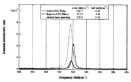
また、上記結晶化の手法によって得られた半導体膜(図中、Improved CG−Siliconと表記)のラマン散乱分光の結果を図18に太線で示す。ここで、比較のため、単結晶シリコン(図中、ref.(100)Si Waferと表記)のラマン散乱分光の結果を細線で示した。また、非晶質珪素膜を形成後、熱処理を行って半導体膜が含有する水素を放出した後、パルス発振のエキシマレーザを用い結晶化を行った半導体膜(図中、excimer laser annealingと表記)のラマン散乱分光の結果を図18に点線で示した。
【0210】
本実施例の手法によって得られた半導体膜のラマンシフトは、517.3cm-1のピークを有する。また、半値幅は、4.96cm-1である。一方、単結晶シリコンのラマンシフトは、520.7cm-1のピークを有する。また、半値幅は、4.44cm-1である。パルス発振のエキシマレーザを用い結晶化を行った半導体膜のラマンシフトは、516.3cm-1である。また、半値幅は6.16cm-1である。
【0211】
図18の結果により、本実施例に示した結晶化の手法によって得られた半導体膜の結晶性が、パルス発振のエキシマレーザを用い結晶化を行った半導体膜の結晶性に比べて単結晶シリコンに近いことがわかる。
【0212】
本実施例で作製された半導体膜は、実施例8、実施例10のTFTの作製工程に適用することができる。
【0213】
(実施例13)
本実施例では、実施例11に示した手法によって結晶化した半導体膜を用いてNチャネルTFTを作製した例について、図15、図19および図21を用いて説明する。
【0214】
本実施例では基板4120として、ガラス基板を用い、ガラス基板上に下地膜4121として、プラズマCVD法により酸化窒化珪素膜(組成比Si=32%、O=27%、N=24%、H=17%)50nm、酸化窒化珪素膜(組成比Si=32%、O=59%、N=7%、H=2%)100nmを積層した。次いで、下地膜4121上に半導体膜4122として、プラズマCVD法により非晶質珪素膜150nmを形成した。そして、500℃で3時間の熱処理を行って、半導体膜が含有する水素を放出させた。(図19(A))
【0215】
その後、レーザ光として連続発振のYVO4レーザの第2高調波(波長532nm、5.5W)を用い、図15で示した光学系における凸レンズ4003に対するレーザ光の入射角φを20°として200μm×50μmの楕円状ビームを形成した。前記楕円状ビームを、50cm/sの速度で相対的に走査して、半導体膜4122に照射した。(図19(B))
【0216】
そして、第1のドーピング処理を行う。これはしきい値を制御するためのチャネルドープである。材料ガスとしてB2H6を用い、ガス流量30sccm、電流密度0.05μA、加速電圧60keV、ドーズ量1×10¹⁴/cm2として行った。(図19(C))
【0217】
続いて、パターニングを行って、半導体膜4124を所望の形状にエッチングした後、エッチングされた半導体膜を覆うゲート絶縁膜4127としてプラズマCVD法により膜厚115nmの酸化窒化珪素膜を形成する。次いで、ゲート絶縁膜4127上に導電膜として膜厚30nmのTaN膜4128と、膜厚370nmのW膜4129を積層形成する。(図19(D))
【0218】
フォトリソグラフィ法を用いてレジストからなるマスク(図示せず)を形成して、W膜、TaN膜、ゲート絶縁膜をエッチングする。
【0219】
そして、レジストからなるマスクを除去して第2のドーピング処理を行い、半導体膜にn型を付与する不純物元素を導入する。この場合、導電層4130、4131がn型を付与する不純物元素に対するマスクとなり、自己整合的に不純物領域4134が形成される。本実施例では第2のド−ピング処理は、半導体膜の膜厚が150nmと厚いため2条件に分けて行った。本実施例では、材料ガスとしてフォスフィン(PH3)を用い、ドーズ量を2×10¹³/cm2とし、加速電圧を90keVとして行った後、ドーズ量を5×1014/cm2とし、加速電圧を10keVとして行った。(図19(E))
【0220】
この工程で、半導体層に不純物領域4134が形成される。
【0221】
次いで、プラズマCVD法により第1の層間絶縁膜4137として膜厚50nmの酸化窒化珪素膜(組成比Si=32.8%、O=63.7%、N=3.5%)を形成した。
【0222】
次いで、熱処理により、半導体層の結晶性の回復、半導体層に添加された不純物元素の活性化を行う。本実施例ではファーネスアニール炉を用いた熱アニール法により、窒素雰囲気中にて550度4時間の熱処理を行った。(図19(F))
【0223】
次いで、第1の層間絶縁膜4137上に無機絶縁膜材料または有機絶縁物材料から成る第2の層間絶縁膜4138を形成する。本実施例では、CVD法により膜厚50nmの窒化珪素膜を形成した後、膜厚400nmの酸化珪素膜を形成した。
【0224】
そして、熱処理を行うと水素化処理を行うことができる。本実施例では、ファーネスアニール炉を用い、410度で1時間、窒素雰囲気中にて熱処理を行った。
【0225】
2つの層間絶縁膜を形成した後にコンタクトホールを形成するためのエッチング工程を行う。ドライエッチングまたはウェットエッチング法を用いて、N型の不純物領域4137、およびソース信号線(図示せず)、およびゲート信号線(図示せず)、電流供給線(図示せず)、およびゲート電極4130に達する(図示せず)コンタクトホールをそれぞれ形成する。
【0226】
続いて、各不純物領域と電気的に接続する配線4139を形成する。本実施例では、膜厚50nmのTi膜と、膜厚500nmのAl―Si膜と、膜厚50nmのTi膜との積層膜をパターニングして形成した。もちろん、二層構造に限らず、単層構造でもよいし、三層以上の積層構造にしてもよい。また、配線の材料としては、AlとTiに限らない。例えば、TaN膜上にAlやCuを形成し、さらにTi膜を形成した積層膜をパターニングして配線を形成してもよい。(図19(G))
【0227】
以上の様にして、チャネル長6μm、チャネル幅4μmのNチャネル型TFT4151が形成された。
【0228】
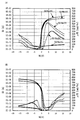
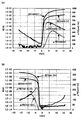
このNチャネル型TFT4151の電気的特性を測定した結果を図21(A)に示す。電気的特性の測定条件は、測定点をそれぞれ2点とし、ゲート電圧Vg=―16〜16Vの範囲で、ドレイン電圧Vd=1V及び5Vとした。また、図21において、ドレイン電流(ID)、ゲート電流(IG)は実線で、移動度(μFE)は点線で示している。
【0229】
本発明を用いて結晶化を行った半導体膜には大粒径の結晶粒が形成されているため、前記半導体膜を用いてTFTを作製すると、そのチャネル形成領域に含まれる結晶粒界の本数を少なくすることができる。さらに、形成された結晶粒は一方向に揃っているため、キャリアが結晶粒界を横切る回数を極端に減らすことができる。そのため、図21に示したように電気的特性の良いTFTが得られる。特に移動度が、Nチャネル型TFTでは524cm2/Vsとなることがわかる。このようなTFTを用いて半導体装置を作製すれば、その動作特性および信頼性をも向上することが可能となる。
【0230】
本実施例で作製された半導体膜は、実施の形態および実施例1〜実施例7のTFTの作製工程に適用することができる。
【0231】
(実施例14)
本実施例では、実施例11に示した手法によって結晶化した半導体膜を用いてPチャネル型TFTを作製した例について、図15、図20および図21を用いて説明する。
【0232】
本実施例では基板4220として、ガラス基板を用い、ガラス基板上に下地膜4221として、プラズマCVD法により酸化窒化珪素膜(組成比Si=32%、O=27%、N=24%、H=17%)50nm、酸化窒化珪素膜(組成比Si=32%、O=59%、N=7%、H=2%)100nmを積層した。次いで、下地膜4221上に半導体膜4222として、プラズマCVD法により非晶質珪素膜150nmを形成した。そして、500℃で3時間の熱処理を行って、半導体膜が含有する水素を放出させた。(図20(A))
【0233】
その後、レーザ光として連続発振のYVO4レーザの第2高調波(波長532nm、5.5W)を用い、図15で示した光学系における凸レンズ4003に対するレーザ光の入射角φを20°として200μm×50μmの楕円状ビームを形成した。前記楕円状ビームを、50cm/sの速度で相対的に走査して、半導体膜4222に照射した。(図20(B))
【0234】
そして、第1のドーピング処理を行う。これはしきい値を制御するためのチャネルドープである。材料ガスとしてB2H6を用い、ガス流量30sccm、電流密度0.05μA、加速電圧60keV、ドーズ量1×10¹⁴/cm2として行った。(図20(C))
【0235】
続いて、パターニングを行って、半導体膜4224を所望の形状にエッチングした後、エッチングされた半導体膜を覆うゲート絶縁膜4227としてプラズマCVD法により膜厚115nmの酸化窒化珪素膜を形成する。次いで、ゲート絶縁膜4227上に導電膜として膜厚30nmのTaN膜4228と、膜厚370nmのW膜4229を積層形成する。(図20(D))
【0236】
フォトリソグラフィ法を用いてレジストからなるマスク(図示せず)を形成して、W膜、TaN膜、ゲート絶縁膜をエッチングする。
【0237】
そして、レジストからなるマスクを除去した後、第2のドーピング処理を行う。第2のドーピング処理により、Pチャネル型TFTの活性層となる半導体膜に不純物元素が添加された不純物領域4236を形成する。導電層4230、4231を不純物元素に対するマスクとして用い、p型を付与する不純物元素を添加して自己整合的に不純物領域4236を形成する。本実施例では第2のド−ピング処理においても、半導体膜の膜厚が150nmと厚いため2条件に分けて行った。本実施例では、材料ガスとしてジボラン(B2H6)を用い、ドーズ量を2×10¹³/cm2とし、加速電圧を90keVとして行った後、ドーズ量を1×1015/cm2とし、加速電圧を10keVとして行った。(図20(E))
【0238】
以上までの工程で、半導体層に不純物領域4236が形成される。
【0239】
次いで、プラズマCVD法により第1の層間絶縁膜4237として膜厚50nmの酸化窒化珪素膜(組成比Si=32.8%、O=63.7%、H=3.5%)を形成した。
【0240】
次いで、熱処理により、半導体層の結晶性の回復、半導体層に添加された不純物元素の活性化を行う。本実施例ではファーネスアニール炉を用いた熱アニール法により、窒素雰囲気中にて550度4時間の熱処理を行った。(図20(F))
【0241】
次いで、第1の層間絶縁膜4237上に無機絶縁膜材料または有機絶縁物材料から成る第2の層間絶縁膜4238を形成する。本実施例では、CVD法により膜厚50nmの窒化珪素膜を形成した後、膜厚400nmの酸化珪素膜を形成した。
【0242】
そして、熱処理を行うと水素化処理を行うことができる。本実施例では、ファーネスアニール炉を用い、410度で1時間、窒素雰囲気中にて熱処理を行った。
【0243】
2つの層間絶縁膜を形成した後にコンタクトホールを形成するためのエッチング工程を行う。ドライエッチングまたはウェットエッチング法を用いて、N型の不純物領域4237、およびソース信号線(図示せず)、およびゲート信号線(図示せず)、電流供給線(図示せず)、およびゲート電極4230に達する(図示せず)コンタクトホールをそれぞれ形成する。
【0244】
続いて、各不純物領域と電気的に接続する配線4239を形成する。本実施例では、膜厚50nmのTi膜と、膜厚500nmのAl―Si膜と、膜厚50nmのTi膜との積層膜をパターニングして形成した。もちろん、二層構造に限らず、単層構造でもよいし、三層以上の積層構造にしてもよい。また、配線の材料としては、AlとTiに限らない。例えば、TaN膜上にAlやCuを形成し、さらにTi膜を形成した積層膜をパターニングして配線を形成してもよい。(図20(G))
【0245】
以上の様にして、チャネル長6μm、チャネル幅4μmのPチャネル型TFT4252が形成された。
【0246】
このPチャネル型TFT4252の電気的特性を測定した結果を図21(B)に示す。電気的特性の測定条件は、測定点をそれぞれ2点とし、ゲート電圧Vg=―16〜16Vの範囲で、ドレイン電圧Vd=1V及び5Vとした。また、図21において、ドレイン電流(ID)、ゲート電流(IG)は実線で、移動度(μFE)は点線で示している。
【0247】
本発明を用いて結晶化を行った半導体膜には大粒径の結晶粒が形成されているため、前記半導体膜を用いてTFTを作製すると、そのチャネル形成領域に含まれる結晶粒界の本数を少なくすることができる。さらに、形成された結晶粒は一方向に揃っているため、キャリアが結晶粒界を横切る回数を極端に減らすことができる。そのため、図21に示したように電気的特性の良いTFTが得られる。特に移動度がPチャネル型TFTでは205cm2/Vsとなることがわかる。このようなTFTを用いて半導体装置を作製すれば、その動作特性および信頼性をも向上することが可能となる。
【0248】
本実施例で作製された半導体膜は、実施の形態および実施例1〜実施例7のTFTの作製工程に適用することができる。
【0249】
(実施例15)
本実施例では、実施例13とは異なる方法で半導体膜の結晶化を行い、前記半導体膜を用いてNチャネルTFTを作製した例について、図15、図22〜図25を用いて説明する。
【0250】
半導体膜として非晶質珪素膜を形成するまでの工程は、実施例13と同様である。なお、非晶質珪素膜は、150nmの厚さで形成した(図22(A))。
【0251】
その後、特開平7−183540号公報に記載された方法を利用し、前記半導体膜上にスピンコート法にて酢酸ニッケル水溶液(重量換算濃度5ppm、体積10ml)を塗布して金属含有層41を形成する。そして、500℃の窒素雰囲気で1時間、550℃の窒素雰囲気で12時間の熱処理を行った。こうして半導体膜4342を得た。(図22(B))
【0252】
続いて、レーザアニール法により、半導体膜4342の結晶性の向上を行う。
【0253】
レーザアニール法の条件は、レーザ光として連続発振のYVO4レーザの第2高調波(波長532nm、5.5W)を用い、図15で示した光学系における凸レンズ4003に対するレーザ光の入射角φを20°として200μm×50μmの楕円状ビームを形成した。前記楕円状ビームを、基板を20cm/sまたは50cm/sの速度で移動させながら照射して、半導体膜4342の結晶性の向上を行った。こうして半導体膜4343を得た。(図22(C))
【0254】
図22(C)の半導体膜の結晶化の後の工程は、実施例7において示した図19(C)〜図19(G)の工程と同様である。こうして、チャネル長6μm、チャネル幅4μmのNチャネル型TFT4151が形成された。これらの電気的特性を測定した。
【0255】
上記工程によって作製したTFTの電気的特性を、図23、図24、図25に示す。
【0256】
図23(A)に、図22(C)のレーザアニール工程において、基板の速度を20cm/sで移動させて作製したNチャネル型TFTの電気的特性を示す。また、図24(A)に、図22(C)のレーザアニール工程において、基板の速度を50cm/sで移動させて作製したNチャネル型TFTの電気的特性を示す。
【0257】
なお、電気的特性の測定条件は、ゲート電圧Vg=―16〜16Vの範囲で、ドレイン電圧Vd=1V及び5Vとした。また、図23、図24において、ドレイン電流(ID)、ゲート電流(IG)は実線で、移動度(μFE)は点線で示している。
【0258】
本発明を用いて結晶化を行った半導体膜には大粒径の結晶粒が形成されているため、前記半導体膜を用いてTFTを作製すると、そのチャネル形成領域に含まれる結晶粒界の本数を少なくすることができる。さらに、形成された結晶粒は一方向に揃っており、レーザ光の相対的な走査方向に対して交差する方向に形成される粒界が少ないため、キャリアが結晶粒界を横切る回数を極端に減らすことができる。
【0259】
そのため、図23及び図24に示したように電気的特性の良いTFTが得られる。特に移動度が、図23では510cm2/Vs、また、図24では595cm2/Vsと非常に優れていることがわかる。そして、このようなTFTを用いて半導体装置を作製すれば、その動作特性および信頼性をも向上することが可能となる。
【0260】
また、図25(A)に、図22(C)のレーザアニール工程において、基板の速度を50cm/sで移動させて作製したNチャネル型TFTの電気的特性を示す。
【0261】
なお、電気的特性の測定条件は、ゲート電圧Vg=―16〜16Vの範囲で、ドレイン電圧Vd=0.1V及び5Vとした。
【0262】
図25(A)に示したように電気的特性の良いTFTが得られる。特に移動度がNチャネル型TFTでは657cm2/Vsと非常に優れていることがわかる。そして、このようなTFTを用いて半導体装置を作製すれば、その動作特性および信頼性をも向上することが可能となる。
【0263】
本実施例で作製された半導体膜は、実施の形態および実施例1〜実施例7のTFTの作製工程に適用することができる。
【0264】
(実施例16)
本実施例では、実施例14とは異なる方法で半導体膜の結晶化を行い、前記半導体膜を用いてPチャネルTFTを作製した例について、図15、図22〜図25を用いて説明する。
【0265】
半導体膜として非晶質珪素膜を形成するまでの工程は、実施例14と同様である。なお、非晶質珪素膜は、150nmの厚さで形成した(図22(A))。
【0266】
その後、特開平7−183540号公報に記載された方法を利用し、前記半導体膜上にスピンコート法にて酢酸ニッケル水溶液(重量換算濃度5ppm、体積10ml)を塗布して金属含有層4341を形成する。そして、500℃の窒素雰囲気で1時間、550℃の窒素雰囲気で12時間の熱処理を行った。こうして半導体膜4342を得た。(図22(B))
【0267】
続いて、レーザアニール法により、半導体膜4342の結晶性の向上を行う。
【0268】
レーザアニール法の条件は、レーザ光として連続発振のYVO4レーザの第2高調波(波長532nm、5.5W)を用い、図15で示した光学系における凸レンズ4003に対するレーザ光の入射角φを20°として200μm×50μmの楕円状ビームを形成した。前記楕円状ビームを、基板を20cm/sまたは50cm/sの速度で移動させながら照射して、半導体膜4342の結晶性の向上を行った。こうして半導体膜4343を得た。(図22(C))
【0269】
図22(C)の半導体膜の結晶化の後の工程は、実施例8において示した図20(C)〜図20(G)の工程と同様である。こうして、チャネル長6μm、チャネル幅4μmのPチャネル型TFT4252が形成された。これらの電気的特性を測定した。
【0270】
上記工程によって作製したTFTの電気的特性を、図23、図24、図25に示す。
【0271】
図23(B)に、図22(C)のレーザアニール工程において、基板の速度を20cm/sで移動させて作製したPチャネル型TFTの電気的特性を示す。また、図24(B)に、図22(C)のレーザアニール工程において、基板の速度を50cm/sで移動させて作製したPチャネル型TFTの電気的特性を示す。
【0272】
なお、電気的特性の測定条件は、ゲート電圧Vg=―16〜16Vの範囲で、ドレイン電圧Vd=1V及び5Vとした。また、図23、図24において、ドレイン電流(ID)、ゲート電流(IG)は実線で、移動度(μFE)は点線で示している。
【0273】
本発明を用いて結晶化を行った半導体膜には大粒径の結晶粒が形成されているため、前記半導体膜を用いてTFTを作製すると、そのチャネル形成領域に含まれる結晶粒界の本数を少なくすることができる。さらに、形成された結晶粒は一方向に揃っており、レーザ光の相対的な走査方向に対して交差する方向に形成される粒界が少ないため、キャリアが結晶粒界を横切る回数を極端に減らすことができる。
【0274】
そのため、図23及び図24に示したように電気的特性の良いTFTが得られる。特に移動度が、図23のPチャネル型TFTでは200cm2/Vs、また、図24でのPチャネル型TFTでは199cm2/Vsと非常に優れていることがわかる。そして、このようなTFTを用いて半導体装置を作製すれば、その動作特性および信頼性をも向上することが可能となる。
【0275】
また、図25(B)に、図22(C)のレーザアニール工程において、基板の速度を50cm/sで移動させて作製したPチャネルTFT4152の電気的特性を示す。
【0276】
なお、電気的特性の測定条件は、ゲート電圧Vg=―16〜16Vの範囲で、ドレイン電圧Vd=0.1V及び5Vとした。
【0277】
図25(B)に示したように電気的特性の良いTFTが得られる。特に移動度がPチャネル型TFTでは219cm2/Vsと非常に優れていることがわかる。そして、このようなTFTを用いて半導体装置を作製すれば、その動作特性および信頼性をも向上することが可能となる。
【0278】
本実施例で作製された半導体膜は、実施の形態および実施例1〜実施例7のTFTの作製工程に適用することができる。
【0279】
(実施例17)
本実施例においては、画素部にEL素子を始めとする発光素子を用いる表示装置の作製工程について説明する。
【0280】
ここで、本明細書において発光素子とは、一重項励起子から基底状態に遷移する際の発光(蛍光)を利用するものと、三重項励起子から基底状態に遷移する際の発光(燐光)を利用するものの両方を示す。
【0281】
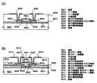
実施例8に示した工程に従い、図8(A)〜図8(B)に示すように、第1および第2の層間絶縁膜まで形成する。
【0282】
続いて、図27(A)に示すようにコンタクトホールを開口する。コンタクトホールの形状は、ドライエッチングまたはウェットエッチングを用い、不純物領域、ソース信号線、ゲート信号線、電流供給線、およびゲート電極に達するようにそれぞれ形成する。
【0283】
次に、EL素子の陽極5001として、ITO等を代表とする透明導電膜を成膜し、所望の形状にパターニングする。Ti、Tiを含むAlおよびTiでなる積層膜を成膜し、所望の形状にパターニングして、配線電極5002〜5005および画素電極5006を形成する。各層の膜厚は、実施例8と同様で良い。画素電極5006は、先に形成した陽極5001と重なるようにして形成してコンタクトを取っている。
【0284】
続いて、アクリルなどの有機樹脂材料、もしくは無機SiO2やプラズマCVD法で作製したSiO2(PCVD-SiO2)、SOG(Spin on Glass;塗布珪素酸化膜)等の無機材料からなる絶縁膜を形成し、EL素子の陽極5001に対応する位置に開口部を形成して第3の層間絶縁膜5007を形成する。ここで、開口部を形成する際、なだらかなテーパー形状の側壁とすることが望ましい。
【0285】
開口部の側壁が十分なだらかなテーパー形状となっていない場合、段差に起因するEL層の劣化、段切れ等が顕著な問題となるため、注意が必要である。第2の層間絶縁膜と第3の層間絶縁膜5007の組み合わせとしては、▲1▼PCVD‐SiO2とPCVD-SiO2、▲2▼SOGとSOG、▲3▼PCVD-SiO2上のSOGとPCVD-SiO2、▲4▼アクリルとアクリル、▲5▼SiO2上のアクリルとPCVD-SiO2、▲6▼SiO2上のPCVD-SiO2とアクリルなどが良い。
【0286】
次に、EL層5008を形成した後、EL素子の陰極5009を、セシウム(Cs)を2[nm]以下の厚さで、および銀(Ag)を10[nm]以下の厚さで形成する。EL素子の陰極5009の膜厚を極めて薄くすることにより、EL層で発生した光は陰極5009を透過して出射される。
【0287】
次いで、EL素子の保護を目的として、保護膜5010を成膜する。その後、FPCの貼付等の作業を行った後、発光装置が完成する。
【0288】
本実施例において、図27(A)に示した発光装置におけるEL素子の構成の詳細を図27(B)に示す。EL素子の陽極5101は、ITOを代表とする透明導電膜でなる。5102は発光層を含むEL層である。EL素子の陰極は、いずれも薄く形成されたCs膜5103およびAg膜5104である。5105が保護膜である。
【0289】
EL素子の陰極側を、きわめて薄い膜厚で形成することにより、EL層5102で発生した光は陰極5103、5104を透過して上方に出射される。つまり、TFTが形成されている領域が、発光面の面積を圧迫することがないため、開口率をほぼ100[%]とすることが出来る。
【0290】
以上の工程では、EL素子の上側を陰極、下側を陽極とした構成について説明したが。EL層の下側の画素電極をTiNなどで形成し、EL層の上側の電極をITO等で形成することによって、EL層の上側を陽極、EL層の下側を陰極とすることも可能である。
【0291】
また、開口率はやや低下するが、EL層の下側を陽極、EL層の上側を陰極とし、EL層の下側の電極をITO等で形成し、EL層の上側の電極については、本実施例と異なり、MgAg等を用いて形成することによって、EL層で発生した光をTFTが形成されている基板側、すなわち下方に出射させる型式とすることも勿論可能である。
【0292】
本実施例は、実施の形態及び実施例1乃至実施例7と自由に組み合わせて実施することが可能である。
【0293】
(実施例18)
本実施例においては、実施例17と異なる方法によって発光素子を用いた表示装置を作製する工程について説明する。
【0294】
実施例8に示した作業工程に従い、図8(A)〜図8(B)に示すように、第1および第2の層間絶縁膜までを形成する。
【0295】
続いて、図28(A)に示すように、コンタクトホールを開口する。コンタクトホールの形状は、ドライエッチングまたはウェットエッチング法を用い、N型の不純物領域、ソース信号線、ゲート信号線、電流供給線、およびゲート電極に達するようにそれぞれ形成する。
【0296】
次に、配線5201〜5204、およびEL素子の陽極となる画素電極5205を、Ti膜、Tiを含むAl膜、Ti膜、および透明導電膜の積層膜として形成する。
【0297】
続いて、アクリルなどの有機樹脂材料、もしくは無機SiO2やプラズマCVD法で作製したSiO2(PCVD-SiO2)、SOG(Spin on Glass;塗布珪素酸化膜)等の無機材料からなる絶縁膜を形成し、EL素子の陽極5205に対応する位置に開口部を形成して第3の層間絶縁膜5206を形成する。ここで、開口部を形成する際、なだらかなテーパー形状の側壁とすることが望ましい。
【0298】
開口部の側壁が十分なだらかなテーパー形状となっていない場合、段差に起因するEL層の劣化、段切れ等が顕著な問題となるため、注意が必要である。第2の層間絶縁膜と第3の層間絶縁膜5206の組み合わせとしては、▲1▼PCVD‐SiO2とPCVD-SiO2、▲2▼SOGとSOG、▲3▼PCVD-SiO2上のSOGとPCVD-SiO2、▲4▼アクリルとアクリル、▲5▼SiO2上のアクリルとPCVD-SiO2、▲6▼SiO2上のPCVD-SiO2とアクリルなどが良い。
【0299】
次に、EL層5207を形成した後、EL素子の陰極5208をセシウム(Cs)を2[nm]以下の厚さで、および銀(Ag)を10[nm]以下の厚さで形成する。EL素子の陰極5009の膜厚を極めて薄くすることにより、EL層で発生した光は陰極5009を透過して出射される。
【0300】
次いで、EL素子の保護を目的として、保護膜5209を成膜する。その後、FPCの貼付等の作業を行った後、発光装置が完成する。
【0301】
本実施例において、図28(A)に示した発光装置におけるEL素子の構成の詳細を図28(B)に示す。EL素子の陽極は、Ti、Al、Tiの積層膜である金属膜5301およびITOを代表とする透明電極膜5302である。5303は発光層を含むEL層である。EL素子の陰極は、いずれも極めて薄く形成されたCs膜7304およびAg膜7305である。7306が保護膜である。
【0302】
本実施例で作製した発光装置は、実施例8で示した発光装置同様、開口率をほぼ100と出来る利点を有する。さらに、配線電極および画素電極の形成において、Ti、Al、Tiの積層でなる金属膜と、透明導電膜とを共通のフォトマスクを用いてパターンニングを行うことが可能であり、フォトマスクの削減、および工程の簡略化が可能となる。
【0303】
以上の工程では、EL層の上側を陰極、下側を陽極とした構成について説明したが、EL層の下側の画素電極をTiNなどで形成し、EL層の上側の電極をITOなどで形成することによって、EL層の上側を陽極、EL層の下側を陰極とすることも可能である。
【0304】
また、開口率はやや低下するが、EL層の下側を陽極、EL層の上側を陰極とし、EL層の下側の電極をITO等で形成し、EL層の上側の電極については、本実施例と異なり、MgAg等を用いて形成することによって、EL層で発生した光をTFTが形成されている基板側、すなわち下方に出射させる型式とすることも勿論可能である。
【0305】
本実施例は、実施の形態及び実施例1乃至実施例7と自由に組み合わせて実施することが可能である。
【0306】
(実施例19)
本発明を用いた電子機器として、ビデオカメラ、デジタルカメラ、ゴーグル型ディスプレイ(ヘッドマウントディスプレイ)、ナビゲーションシステム、音響再生装置(カーオーディオ、オーディオコンポ等)、ノート型パーソナルコンピュータ、ゲーム機器、携帯情報端末(モバイルコンピュータ、携帯電話、携帯型ゲーム機または電子書籍等)、記録媒体を備えた画像再生装置(具体的にはDigital Versatile Disc(DVD)等の記録媒体を再生し、その画像を表示しうるディスプレイを備えた装置)などが挙げられる。それらの電子機器の具体例を図29に示す。
【0307】
図29(A)は表示装置であり、筐体1401、支持台1402、表示部1403を含む。本発明は表示部1403を有する表示装置の駆動回路に適用が可能である。
【0308】
図29(B)はビデオカメラであり、本体1411、表示部1412、音声入力1413、操作スイッチ1414、操作スイッチ1415、バッテリー1416、受像部1417などによって構成されている。本発明は表示部1417を有する表示装置の駆動回路に適用が可能である。
【0309】
図29(C)はノート型のパーソナルコンピュータであり、本体1421、筐体1422、表示部1423、キーボード1424などによって構成されている。本発明は表示部1423を有する表示装置の駆動回路に適用が可能である。
【0310】
図29(D)は携帯情報端末であり、本体1431、表示部1432、操作ボタン1433、外部インターフェイス1434などによって構成されている。本発明は表示部1432を有する表示装置の駆動回路に適用が可能である。
【0311】
図29(E)は音響再生装置、具体的には車載用のオーディオ装置であり、本体1441、表示部1442、操作スイッチ1443、1444などによって構成されている。本発明は表示部1442を有する表示装置の駆動回路に適用が可能である。また、今回は車載用オーディオ装置を例に上げたが、携帯型もしくは家庭用オーディオ装置に用いてもよい。
【0312】
図29(F)はデジタルカメラであり、本体1451、表示部(A)1452、接眼部1453、操作スイッチ1454、表示部(B)1455、バッテリー1456などによって構成されている。本発明は表示部(A)1452および表示部(B)1455を有する表示装置の駆動回路に適用が可能である。
【0313】
図29(G)は携帯電話であり、本体1461、音声出力部1462、音声入力部1463、表示部1464、操作スイッチ1465、アンテナ1466などによって構成されている。本発明は表示部1464を有する表示装置の駆動回路に適用が可能である。
【0314】
これらの電子機器に使われる表示装置はガラス基板だけでなく耐熱性のプラスチック基板を用いることもできる。それによってよりいっそうの軽量化を図ることができる。
【0315】
なお、本実施例に示した例はごく一例であり、これらの用途に限定するものではないことを付記する。
【0316】
本実施例は、実施の形態及び実施例1乃至実施例7と自由に組み合わせて実施することが可能である。
【発明の効果】
本発明によって、デジタル映像信号の入力に対して、非反転出力、反転出力の2出力が得られるため、それらの信号によって駆動される後段のバッファにおいては、電流パスの発生を最小限に抑えることが出来る半導体装置を提供することができる。また、上述した構成を用いることにより、消費電力を低減した半導体装置を提供することができる。
【0317】
さらに本発明は、全てのTFTを単極性とした半導体装置を提供することができる。そのため、TFTの製造工程において、不純物元素を添加する工程などの作製工程の一部を省略して、コストの上昇や歩留まりの低下の影響を抑制することができる半導体装置を提供することが出来る、
【0318】
【図面の簡単な説明】
【図1】 本発明の実施形態を示す図。
【図2】 表示装置の概略および断面図。
【図3】 本発明のラッチ回路を用いて構成したソース信号線駆動回路の構成図。
【図4】 ゲート信号線駆動回路の構成図。
【図5】 単極性のTFTを用いて構成したシフトレジスタを示す図。
【図6】 単極性のTFTを用いて構成したラッチ回路およびバッファを示す図。
【図7】 表示装置の作製工程例を示す図。
【図8】 表示装置の作製工程例を示す図。
【図9】 表示装置の作製工程例を示す図。
【図10】 ソース信号線駆動回路の構成を示す図。
【図11】 実施形態に小変更を加えた本発明の実施例を示す図。
【図12】 実施形態に小変更を加えた本発明の実施例を示す図。
【図13】 実施形態と異なる本発明の実施例を示す図。
【図14】 本発明を適用したラッチ回路・バッファ回路の構成例を示す図。
【図15】 実施例8〜13で用いる光学系の模式図。
【図16】 実施例8を行った結果のSEM像を示した図。
【図17】 実施例9を行った結果のSEM像を示した図。
【図18】 実施例9によって得られた半導体膜のラマン散乱分光の結果を示す図。
【図19】 単極性TFTの作製工程例を示す図。
【図20】 単極性TFTの作製工程例を示す図。
【図21】 実施例10および11で作製されたTFTの電気的特性を示す図。
【図22】 レーザーによる半導体膜の処理の工程例を示す図。
【図23】 実施例12および13で作製されたTFTの電気的特性を示す図。
【図24】 実施例12および13で作製されたTFTの電気的特性を示す図。
【図25】 実施例12および13で作製されたTFTの電気的特性を示す図。
【図26】 ボトムゲートおよびデュアルゲート構造のTFTの構造を示す図。
【図27】 発光装置の作製工程例を示す図。
【図28】 発光装置の作製工程例を示す図。
【図29】 本発明の適用が可能な電子機器の例を示す図。
【図30】 実施形態と異なる本発明の実施例を示す図。
【図31】 実施形態と異なる本発明の実施例を示す図。
【図32】 第1のラッチ回路の後段に振幅補償用バッファ回路を追加した実施例の回路図。
【図33】 本発明のラッチ回路の構成。[0001]
BACKGROUND OF THE INVENTION
The present invention relates to a technology of a semiconductor device. The semiconductor device includes a liquid crystal display device using a liquid crystal element for a pixel and a display device using a light emitting element such as an electroluminescence (EL) element. In addition, a circuit for inputting a video signal to a pixel arranged in the display device and performing processing for displaying a video is included. Furthermore, a pulse output circuit including a shift register circuit, a latch circuit, a buffer circuit, a level shift circuit and the like, and an amplifier circuit including an amplifier and the like are included.
[0002]
[Prior art]
In recent years, semiconductor devices in which a semiconductor thin film is formed on an insulator such as a glass substrate, particularly active matrix display devices such as liquid crystal display devices using thin film transistors (hereinafter referred to as TFTs), have been used in many products. Is popular. An active matrix display device has hundreds of thousands to millions of pixels arranged in a matrix, and displays video by controlling the luminance of each pixel by a TFT arranged in each pixel. .
[0003]
Further, a technique for integrally forming a pixel portion and a peripheral circuit on the same substrate using a polysilicon TFT has been developed. The technology greatly contributes to the downsizing and low power consumption of the device, and accordingly, it is used for a display unit of a portable information terminal in which the application field of the technology is remarkably expanded.
[0004]
Here, an example in which the peripheral circuit of the pixel portion is formed on the same substrate using the polysilicon TFT will be described with reference to FIG. Note that FIG. 10 illustrates a source signal line driver circuit as an example of a semiconductor device used for a display device, and the structure and operation thereof are described below.
[0005]
In FIG. 10, the source signal line driver circuit includes a plurality of stages of
[0006]
Although not particularly shown, a buffer or the like may be provided, and the number of bits of the digital video signal is not limited to 3 bits.
[0007]
Next, the operation of the source signal line driving circuit will be briefly described below. In accordance with the input of the clock signal (S_CK), the inverted clock signal (S_CKB), and the start pulse (S_SP), the shift register 1000 sequentially outputs sampling pulses. The
[0008]
[Problems to be solved by the invention]
In the semiconductor device described above, a CMOS circuit in which an N-channel TFT and a P-channel TFT are combined is often used. However, forming a CMOS circuit combining an N-channel TFT and a P-channel TFT on the same insulating surface means forming TFTs having opposite conductivity types on the same insulating surface. Therefore, the manufacturing process is inevitably complicated. As a result, the cost of the semiconductor device increases and the yield decreases.
[0009]
Therefore, a semiconductor device in which all TFTs are unipolar has been devised. When all the TFTs are unipolar, a part of a manufacturing process such as a process of adding an impurity element in the manufacturing process of the TFT can be omitted, and an influence of an increase in cost and a decrease in yield can be suppressed.
[0010]
An example of a semiconductor device in which all TFTs are unipolar will be described with reference to FIG. FIG. 5A shows a shift register including unipolar TFTs. The shift register includes a plurality of stages of
[0011]
In FIG. 5B, when a logic circuit is formed by unipolar TFTs, for example, when an N-channel TFT is used, an output signal is generated depending on the threshold value of the N-channel TFT connected to the high potential side power supply. There is a problem that the amplitude of (SR OUT) is attenuated as compared with the amplitude of the input signals (in_L, in_R). The
[0012]
Note that in this specification, since a digital circuit is used, the input / output potential is represented by a binary value of Hi or Lo. Since the meanings of Hi and Lo are reversed in the N channel type and the P channel type, the terms active potential and inactive potential may be used. Further, the active potential refers to a Hi potential in a circuit composed of only N-channel transistors or a Lo potential in a circuit composed of only P-channel transistors. Further, the inactive potential refers to a Lo potential in a circuit composed of only N-channel transistors or a Hi potential in a circuit composed of only P-channel transistors.
[0013]
Hi / Lo or the active potential / inactive potential does not necessarily match the power supply potential (VDD / VSS), and may be the same when viewed as a binary value. For example, a potential that is lower than VDD by a threshold value by an N-channel transistor is also included in the Hi potential. A potential that can be recovered to VDD / VSS by an amplitude compensation circuit or the like is considered to be the same Hi / Lo or active potential / inactive potential.
[0014]
Next, operation of the circuit illustrated in FIG. 5B will be briefly described. Here, the unipolar TFT constituting the circuit is an N-channel TFT, and its threshold voltage is uniformly VthN. However, this does not limit the TFT constituting the circuit to the N-channel type. Only the P-channel type can be used as the TFT constituting the circuit.
[0015]
When describing the circuit operation, the operation of the TFT may be described. When the TFT is turned on, the absolute value of the gate-source voltage of the TFT exceeds the absolute value of the threshold voltage of the TFT, and the TFT is turned on. The source and drain regions of the TFT become conductive through the channel formation region. When the TFT is turned off, the absolute value of the gate-source voltage of the TFT is lower than the absolute value of the threshold voltage of the TFT. In this case, the source region and the drain region of the TFT are turned off.
[0016]
In order to explain the connection of TFTs, “gate electrode, input electrode, output electrode” and “gate electrode, source region, drain region” are properly used. This is because in many cases the gate-source voltage is considered when explaining the operation of the TFT, but it is difficult to clearly distinguish the TFT source and drain regions because of the TFT configuration. When describing the output, it is referred to as an input electrode or an output electrode. When describing the relationship between the potentials of the TFT electrodes, one of the input electrode and the output electrode is referred to as a source region, and the other as a drain region. I will decide.
[0017]
Further, the amplitude of the signal in the description is VDD-VSS, the high-potential side power supply is VDD, and the low-potential side potential is VSS. Further, VthN <(VDD−VthN) is satisfied. In order to simplify the relationship between the potentials, VSS = 0 [V] is considered. However, this does not apply when the circuit is actually driven.
[0018]
In FIG. 5B, the (m−1) th stage output pulse is input to the gate electrodes of the
[0019]
On the other hand, the gate electrodes of the
[0020]
Here, a capacitor means 507 is provided between the gate electrode and the output electrode of the
[0021]
Similarly, a pulse is output according to S-CKB at the (m + 1) th stage. The (m + 1) th stage output pulse is fed back to the mth stage and input to the gate electrodes of the
[0022]
Next, FIG. 6A shows an example in which a latch circuit is configured by unipolar TFTs. A circuit indicated by a dotted
[0023]
The
[0024]
The
[0025]
The
[0026]
When the Hi potential is input to the gate electrodes of the
[0027]
When the Lo potential is input to the gate electrodes of the
[0028]
Note that a buffer may be provided between the
[0029]
Here, attention is focused on the
[0030]
The present invention has been made in view of the above-described problems, and an object of the present invention is to provide a semiconductor device with reduced power consumption in a semiconductor device including unipolar TFTs.
[0031]
[Means for Solving the Problems]
The latch circuit having the configuration of the switching TFT and the capacitor means shown in FIG. 6A is a one-input one-output type. Therefore, the
[0032]
Therefore, the present invention provides a semiconductor device having a configuration in which the output of the latch circuit is a two-output type of output and inverted output.
[0033]
FIG. 33 shows a latch circuit as an example of the semiconductor device of the present invention. The latch circuit includes a
[0034]
The
[0035]
Capacitance means 1303 is connected to the inverted output (Data Out_b). The capacitor means 1303 may not be provided when it is not particularly necessary to hold the output signal or depending on the circuit configuration of the subsequent stage.
[0036]
A sampling pulse (Samp. Pulse) and a digital video signal (Digital Data) are input to the second circuit 1302. The second circuit 1302 outputs an output (Data Out).
[0037]
Capacitance means 1304 is connected to the output (Data Out). This capacitor means 1304 may not be necessary depending on the circuit configuration of the subsequent stage.
[0038]
Further, the
[0039]
(1) The TFTs constituting the first circuit and the second circuit are all unipolar.
(2) In the first circuit, the through current flows only when both the sampling pulse (Samp. Pulse) and the digital video signal (Digital Data) are Hi.
(3) In the first circuit, when the sampling pulse (Samp.Pulse) is Hi, an inverted signal of the digital video signal (Digital Data) is output to the inverted output (Data Out_b).
(4) In the second circuit, when the sampling pulse (Samp.Pulse) is Hi, a digital video signal (Digital Data) is output to the output (Data Out).
(5) In the first circuit and the second circuit, when the sampling pulse (Samp.Pulse) is Lo, the output (Data Out) and the inverted output (Data Out_b) are in a floating state.
[0040]
In (2), it is assumed that the through current is a through current between the high potential side power source VDD and the low potential side power source VSS or a through current between the sampling pulse (Samp. Pulse) and the low potential side power source VSS.
[0041]
In (3) or (4), when the inverted output (Data Out_b) or the output (Data Out) is Hi, the buffer circuit having a threshold compensation function performs the inverted output (Data Out_b) or the output (Data Out). Is a potential that can be restored to the high potential side power supply VDD.
[0042]
In addition, in (3) or (4), the inverted output (Data Out_b) or the output (Data Out) is Lo, which means that the inverted output (Data Out_b) or the output (Data Out) is supplied from the low potential side power supply by the buffer circuit. It means a potential that can be the same potential as VSS.
[0043]
In (5), the fact that the output (Data Out) and the inverted output (Data Out_b) are in the floating state does not have to be strictly in the floating state. It is sufficient that the potentials of the output (Data Out) and the inverted output (Data Out_b) have an impedance that can be held for a predetermined time (typically, one horizontal period) including the subsequent circuit.
[0044]
The present invention provides a semiconductor device including a circuit configuration that satisfies the above-described properties. Further, according to the present invention, non-inverted output and inverted output can be obtained with respect to the input of the digital video signal, so that the generation of a current path is minimized in the subsequent buffer driven by these signals. Provided is a semiconductor device. Furthermore, a semiconductor device with reduced power consumption is provided by using the above structure.
[0045]
DETAILED DESCRIPTION OF THE INVENTION
As an example of the semiconductor device of the present invention, a latch circuit is shown in FIG.
[0046]
The latch circuit shown in FIG. 1 includes
[0047]
A feature of this configuration is that two outputs, an output (Data Out) and an inverted output (Data Out_b), are obtained with respect to the input of the digital video signal.
[0048]
Next, the operation of the latch circuit illustrated in FIG. 1 will be described. Note that both the sampling pulse and the digital video signal have an input amplitude between VDD and VSS.
[0049]
The sampling pulse output from the shift register is input to the gate electrodes of the
[0050]
At this time, both the
[0051]
On the other hand, when the input digital video signal is at the Lo potential, the Lo potential is input to the gate electrode of the
[0052]
The above operations are sequentially performed for one horizontal cycle. The signals output to the output terminal (Data Out) and the inverted output terminal (Data Out_b) are held by the capacitance means 106 and 107 until the retrace period, respectively. Note that the capacitor means 106 and 107 may not be provided depending on the circuit configuration of the subsequent stage and the length of the horizontal period.
[0053]
When the sampling pulse (Samp. Pulse) becomes Lo potential and the sampling period ends, the
[0054]
In the latch circuit of the present invention shown in FIG. 1, a current path is generated between VDD-TFT101-TFT102-VSS only when a sampling pulse is input and a digital video signal is at a Hi potential. .
[0055]
Here, the amplitude of the output signal appearing on the output terminal (Data Out) side is affected by the threshold value of the
[0056]
In the circuit shown in FIG. 1, the positions of the
[0057]
Although FIG. 1 shows the case where the
[0058]
【Example】
Example 1
In this embodiment, a latch circuit having a structure different from that of the embodiment mode is described with reference to FIGS.
[0059]
FIG. 11 shows a modification of the connection of the latch circuit of the present invention shown in FIG. In FIG. 11, the same numbers are used for portions corresponding to FIG.
[0060]
In FIG. 1, the gate electrode and the input electrode of the
[0061]
In the above configuration, the potential of the gate electrode of the
[0062]
The capacitor means 106 and 107 may not be required depending on the circuit configuration of the subsequent stage and the length of the horizontal period. Further, the positions of the
[0063]
Although this embodiment shows the case where the TFT is an N-channel type, the present invention can also be applied to a case where the TFT is a P-channel type.
[0064]
(Example 2)
In this embodiment, a latch circuit having a structure different from that of the embodiment mode and
[0065]
FIG. 12 shows a modification of the connection of the latch circuit of the present invention shown in FIG. In FIG. 12, the same numbers are used for portions corresponding to FIG.
[0066]
In FIG. 1, a diode-connected
[0067]
The capacitor means 106 and 107 may not be required depending on the circuit configuration of the subsequent stage and the length of the horizontal period. Further, the positions of the
[0068]
Although this embodiment shows the case where the TFT is an N-channel type, the present invention can also be applied to a case where the TFT is a P-channel type.
[0069]
(Example 3)
In this embodiment, a latch circuit having a structure different from that of the embodiment mode and Embodiments 1 and 2 will be described with reference to FIG.
[0070]
The latch circuit of the present invention shown in FIG. 13 includes
[0071]
The input electrode of the
[0072]
Next, the operation of the latch circuit illustrated in FIG. 13 is described below. Note that the amplitude at the time of input of the sampling pulse and the digital video signal is between VDD and VSS.
[0073]
The sampling pulse output from the shift register is input to the gate electrodes of the
[0074]
At this time, the
[0075]
On the other hand, when the input digital video signal is at the Lo potential, the Lo potential is input to the gate electrode of the
[0076]
The above operations are sequentially performed for one horizontal cycle. The signals output to the output terminal (Data Out) and the inverted output terminal (Data Out_b) are held by the capacitive means 135 and 136 until the blanking period, respectively. Note that the capacitor means 106 and 107 may not be provided depending on the circuit configuration of the subsequent stage and the length of the horizontal period.
[0077]
When the sampling pulse (Samp. Pulse) becomes the Lo potential and the sampling period ends, the
[0078]
In the latch circuit of the present invention shown in FIG. 13, a current path is generated between VDD-TFT133-TFT131-TFT132-VSS when a sampling pulse is input and the digital video signal is at a Hi potential. Limited.
[0079]
Here, since the amplitude of the output signal appearing on the output terminal (Data Out) side is affected by the threshold value of the
[0080]
Note that in the circuit shown in FIG. 13, the positions of the
[0081]
Although FIG. 13 shows the case where the
[0082]
Example 4
In this embodiment, a latch circuit having a structure different from that in Embodiment Mode and
[0083]
The latch circuit shown in FIG. 30 is obtained by adding a small change to the connection of the latch circuit of the present invention shown in FIG. In FIG. 13, the input electrode of the
[0084]
Since the operation of the latch circuit shown in FIG. 30 is the same as that of the latch circuit shown in FIG. 13 described in the third embodiment, the description thereof is omitted in this embodiment.
[0085]
The capacitor means 135 and 136 may not be necessary depending on the circuit configuration of the subsequent stage and the length of the horizontal period. Further, the positions of the
[0086]
Although this embodiment shows the case where the TFT is an N-channel type, the present invention can also be applied to a case where the TFT is a P-channel type.
[0087]
(Example 5)
In this embodiment, a latch circuit having a structure different from that in Embodiment Mode and
[0088]
The latch circuit shown in FIG. 31 is obtained by making a minor change to the connection of the latch circuit of the present invention shown in FIG. In FIG. 13, the input electrode of the
[0089]
The operation of the latch circuit shown in FIG. 31 is the same as that of the latch circuit shown in FIG. 13 described in the third embodiment, and thus description thereof is omitted in this embodiment.
[0090]
Note that the capacitor means 135 and 136 may not be necessary depending on the circuit configuration of the subsequent stage and the length of the horizontal period. Further, the positions of the
The circuit shown in FIG. 30 is a circuit that satisfies all the characteristics of the latch circuit of the present invention described in the means for solving the problems.
[0091]
Although this embodiment shows the case where the TFT is an N-channel type, the present invention can also be applied to a case where the TFT is a P-channel type.
[0092]
(Example 6)
In this embodiment, the structure and operation of a latch circuit having a structure different from that in Embodiment Mode and
[0093]
FIG. 14 shows an example in which the circuit having the configuration described in the embodiment is a first latch circuit, and the second latch circuit and the buffer are configured. The
[0094]
When a latch pulse (Latch Pulse) is input during a blanking period after sampling for one horizontal period is completed, the
[0095]
When the sampling pulse (Samp. Pulse) becomes Lo potential and the sampling period ends, the
[0096]
Subsequently, an output signal from the
[0097]
When one output (Data Out2) of the
[0098]
At this time, since the potential of the gate electrode of the
[0099]
Here, if VthN <(VDD−VthN), the
[0100]
As a result, when the potential of the gate electrode of the
[0101]
On the other hand, when one output (Data Out2) of the
[0102]
The operation of the inverter composed of the
[0103]
In the latch circuit shown in this embodiment, the first latch circuit to the second latch circuit have an amplitude attenuation corresponding to the threshold value of the TFT, so that the power supply voltage needs to be high to some extent. Thus, the output of the first latch circuit may be configured to compensate the amplitude once through a buffer.
[0104]
In this embodiment, the capacity means 1120 and 1121 may not be provided. When the
[0105]
Although this embodiment shows the case where the TFT is an N-channel type, the present invention can also be applied to a case where the TFT is a P-channel type.
[0106]
This embodiment can be implemented by being freely combined with the embodiment mode and
[0107]
(Example 7)
In the above-described sixth embodiment, the output from the first latch circuit is immediately input to the second latch circuit, and the amplitude attenuation compensation is performed by the buffer circuit arranged at the subsequent stage of the second latch circuit. Yes. However, in this case, if the operating voltage is low and the threshold value of the TFT is large, the original amplitude is greatly affected by the attenuation of the threshold value, and the normal holding operation cannot be performed in the latch circuit. It is done.
[0108]
Therefore, in this embodiment, a semiconductor device having a configuration in which an amplitude compensation buffer circuit is added after the first latch circuit will be described.
[0109]
FIG. 32 shows the structure of the semiconductor device of the present invention. A portion surrounded by a dotted line frame 1201 is the first latch circuit described in the embodiment mode, and includes
[0110]
A portion surrounded by a dotted
[0111]
Next, operation of the semiconductor device illustrated in FIG. 32 is described. Here, the circuit configured by the
[0112]
A sampling pulse (Samp.Pulse) and a digital video signal (Digital Data) are input to the first latch circuit 1201, and a first output signal (Data Out) and a second output signal (Data Out_b) are output. The
[0113]
A signal output from the output electrode of the
[0114]
When the digital video signal (Digital Data) input to the first latch circuit is Hi potential, the first output signal is Hi potential and the second output signal is Lo potential, and is input to the first latch circuit. When the digital video signal (Digital Data) is at the Lo potential, the first output signal is the Lo potential and the second output signal is the Hi potential.
[0115]
Here, the amplitudes of the first and second output signals are between (VDD−VthN) −VSS because they are affected by the threshold values of the
[0116]
When the first output signal is the Lo potential and the second output signal is the Hi potential, the Hi potential is input to the gate electrode of the
[0117]
On the other hand, when the sampling period ends in the first latch circuit, the sampling pulse becomes Lo potential, and the
[0118]
At this time, the potential of the gate electrode of the
[0119]
Here, the bootstrap is activated by the capacitive coupling between the gate electrode and the output electrode of the
[0120]
On the other hand, when the Lo potential is input to the gate electrode of the
[0121]
The above operation is similarly performed in the circuit constituted by the
[0122]
Therefore, the amplitude of the output of the first latch circuit is compensated, and the amplitude between VDD and VSS can be normally obtained and input to the second latch circuit.
[0123]
Here, when the bootstrap works between the gate electrode and the output electrode of the
[0124]
In FIG. 32, the capacity of the capacity means 1216 and 1217 is preferably small. This is because if the capacitance of the capacitance means 1216 and 1217 is large, the rising width of the gate electrodes of the
[0125]
Although this embodiment shows the case where the TFT is an N-channel type, the present invention can also be applied to a case where the TFT is a P-channel type.
[0126]
This embodiment can be implemented by being freely combined with the embodiment mode and
[0127]
(Example 8)
In this embodiment, a method for manufacturing a pixel portion and TFTs of a driver circuit provided around the pixel portion on the same substrate will be described. In addition, although the manufacturing process of a liquid crystal display circuit is mentioned as an example, of course, this invention is not limited to a liquid crystal display device.
[0128]
First, as shown in FIG. 7A, glass such as barium borosilicate glass represented by Corning # 7059 glass or # 1737 glass or aluminoborosilicate glass, or a
[0129]
The island-shaped
[0130]
In order to fabricate a crystalline semiconductor film by laser crystallization, a pulse oscillation type or continuous emission type excimer laser, YAG laser, YVO Four Use a laser. When these lasers are used, it is preferable to use a method in which laser light emitted from a laser oscillator is linearly collected by an optical system and irradiated onto a semiconductor film. The conditions for crystallization are appropriately selected by the practitioner. When an excimer laser is used, the pulse oscillation frequency is 30 [Hz] and the laser energy density is 100 to 400 [mJ / cm. 2 ] (Typically 200-300 [mJ / cm 2 ]). When a YAG laser is used, the second harmonic is used and the pulse oscillation frequency is set to 1 to 10 [kHz], and the laser energy density is set to 300 to 600 [mJ / cm. 2 ] (Typically 350-500 [mJ / cm 2 ]) Then, a laser beam condensed in a linear shape with a width of 100 to 1000 [μm], for example, 400 [μm] is irradiated over the entire surface of the substrate, and the superposition ratio (overlap ratio) of the linear laser light at this time is 80 Perform as ~ 98 [%].
[0131]
Next, a
[0132]
Then, a first
[0133]
The Ta film is formed by sputtering, and a Ta target is sputtered with Ar. In this case, when an appropriate amount of Xe or Kr is added to Ar, the internal stress of the Ta film can be relieved and peeling of the film can be prevented. The resistivity of the α-phase Ta film is about 20 [μΩcm] and can be used for the gate electrode, but the resistivity of the β-phase Ta film is about 180 [μΩcm] and is used as the gate electrode. It is unsuitable. In order to form an α-phase Ta film, tantalum nitride (TaN) having a crystal structure close to that of the α-phase of Ta is formed on the Ta base with a thickness of about 10 to 50 nm. A Ta film can be easily obtained.
[0134]
When forming a W film, it is formed by sputtering using W as a target. In addition, tungsten hexafluoride (WF 6 It can also be formed by a thermal CVD method using In any case, in order to use as a gate electrode, it is necessary to reduce the resistance, and it is desirable that the resistivity of the W film be 20 [μΩcm] or less. Although the resistivity of the W film can be reduced by increasing the crystal grains, if the impurity element such as oxygen is large in W, the crystallization is hindered and the resistance is increased. From this, in the case of the sputtering method, by using a W target having a purity of 99.9999 [%] and further forming a W film with sufficient consideration so that impurities are not mixed in from the gas phase during film formation, A resistivity of 9 to 20 [μΩcm] can be realized.
[0135]
Note that in this embodiment, the first
[0136]
Next, resist
[0137]
Under the above etching conditions, by making the shape of the resist mask suitable, the end portions of the first conductive layer and the second conductive layer are tapered due to the effect of the bias voltage applied to the substrate side. The angle of the tapered portion is 15 to 45 °. In order to perform etching without leaving a residue on the gate insulating film, it is preferable to increase the etching time at a rate of about 10 to 20%. Since the selection ratio of the silicon oxynitride film to the W film is 2 to 4 (typically 3), the surface where the silicon oxynitride film is exposed is etched by about 20 to 50 [nm] by the overetching process. become. Thus, the first shape
[0138]
Subsequently, as shown in FIG. 7C, a second etching process is performed without removing the resist
[0139]
CF of W film and Ta film Four And Cl 2 The etching reaction by the mixed gas can be estimated from the generated radical or ion species and the vapor pressure of the reaction product. Comparing the vapor pressure of fluoride and chloride of W and Ta, WF, which is fluoride of W 6 Is extremely high, other WCl Five , TaF Five , TaCl Five Are comparable. Therefore, CF Four And Cl 2 With this mixed gas, both the W film and the Ta film are etched. However, an appropriate amount of O is added to this mixed gas. 2 When CF is added Four And O 2 Reacts to CO and F, and a large amount of F radicals or F ions are generated. As a result, the etching rate of the W film having a high fluoride vapor pressure is increased. On the other hand, the increase in etching rate of Ta is relatively small even when F increases. Further, since Ta is more easily oxidized than W, O 2 When Ta is added, the surface of Ta is oxidized. Since the Ta oxide does not react with fluorine or chlorine, the etching rate of the Ta film further decreases. Therefore, it is possible to make a difference in the etching rate between the W film and the Ta film, and the etching rate of the W film can be made larger than that of the Ta film.
[0140]
Then, an impurity element imparting n-type conductivity is added by performing a first doping process. As a doping method, an ion doping method or an ion implantation method may be used. The condition of the ion doping method is a dose of 1 × 10 13 ~ 5x10 14 [atoms / cm 2 The acceleration voltage is set to 60 to 100 [keV]. As an impurity element imparting n-type, an element belonging to
[0141]
Then, as shown in FIG. 7D, a second doping process is performed after a portion to be the pixel portion TFT is covered with a resist
[0142]
Through the above steps, impurity regions are formed in each island-like semiconductor layer. The third shape
[0143]
After the resist
[0144]
Further, a heat treatment is performed at 300 to 450 [° C.] for 1 to 12 hours in an atmosphere containing 3 to 100 [%] hydrogen to perform a step of hydrogenating the island-shaped semiconductor layer. This step is a step of terminating dangling bonds in the semiconductor layer with thermally excited hydrogen. As another means of hydrogenation, plasma hydrogenation (using hydrogen excited by plasma) may be performed (FIG. 8A).
[0145]
Next, as shown in FIG. 8B, the first
[0146]
Alternatively, an inorganic material can be used for the second
[0147]
After forming the two interlayer insulating films, an etching process for forming a contact hole is performed. Using dry etching or wet etching, N-
[0148]
Further, as the
[0149]
Subsequently, a
[0150]
On the other hand, a counter electrode 3041 is formed in the pixel portion as shown in FIG. The counter electrode is formed using a transparent conductive material of ITO. In order to keep the visible light transmittance high, it is desirable that the thickness of the counter electrode be 100 [nm] to 120 [nm].
[0151]
[0152]
Subsequently, the
[0153]
Although not particularly shown in the present embodiment, it is possible to improve the uniformity of the cell gap by forming spacers in the pixels by spraying or patterning. In this example, a photosensitive resin film was formed and patterned to form a spacer having a height of 4.0 [μm].
[0154]
Subsequently, the active matrix substrate and the counter substrate are bonded to each other with a
[0155]
Subsequently, a
[0156]
After the injection of the liquid crystal material is completed, the injection port is sealed with a UV curable resin or the like. Thereafter, a polarizing plate is attached by a known method. Finally, the element formed on the substrate is completed as a product by attaching a connector (flexible printed circuit: FPC) for connecting a terminal routed from the circuit and an external signal terminal (FIG. 8C). . In this specification, such a state that can be shipped is called a liquid crystal display device.
[0157]
Further, according to the steps shown in this specification, the number of photomasks necessary for manufacturing an active matrix substrate is five (an island-shaped semiconductor layer pattern, a first wiring pattern (source signal line, a capacitor wiring), a mask pattern , Contact hole pattern, second wiring pattern (including pixel electrode and connection electrode)). As a result, the process can be shortened, and the manufacturing cost can be reduced and the yield can be improved.
[0158]
In the embodiment, an NMOS-structure TFT is shown, but a latch circuit as shown in FIG. 1 can be formed using such a TFT.
[0159]
In this embodiment, the writing TFT has a double gate structure, but may have a single gate structure, a triple gate structure, or a multi-gate structure.
[0160]
In this embodiment, the top gate type TFT is described as an example of the TFT type. In addition, a gate electrode is formed below the active layer as shown in FIG. The bottom gate type TFT or a dual gate type TFT having gate electrodes on the upper and lower sides so as to sandwich the active layer as shown in FIG.
[0161]
This embodiment can be implemented by being freely combined with the embodiment mode and
[0162]
Example 9
In this example, with reference to the circuit shown in the embodiment mode, the circuit shown in Example 1 to Example 7, and the manufacturing process of the TFT shown in Example 8, a TFT was manufactured and the display device ( An example of creating a semiconductor device will be described.
[0163]
FIG. 2A is a schematic view of a display device. A
[0164]
Signals input from the outside to drive the source signal
[0165]
In FIG. 2A, a cross-sectional view taken along the broken line AA ′ is shown in FIG. On the
[0166]
The lead-out
[0167]
The configuration of the source signal
[0168]
The D /
[0169]
In the D /
[0170]
In addition, since the signal input from the outside is output from an integrated circuit such as an IC, it is often a signal having a low voltage amplitude of about 3 [V] to 5 [V] in accordance with the recent decrease in voltage. Therefore, the signal is converted into a signal having a high voltage amplitude by each
[0171]
The configuration of the gate signal line driver circuit 207 is shown in FIG. The shift register indicated by a
[0172]
In addition, since the signal input from the outside is output from an integrated circuit such as an IC, it is often a signal having a low voltage amplitude of about 3 [V] to 5 [V] in accordance with the recent decrease in voltage. Therefore, the signal is converted into a signal having a high voltage amplitude by the
[0173]
This embodiment can be implemented by being freely combined with the embodiment mode and
[0174]
(Example 10)
Although the process shown in
[0175]
In the case of an N-channel TFT, an impurity region called an overlap region is provided in a region overlapping with the gate electrode in order to suppress hot carrier deterioration and the like. On the other hand, in the case of a P-channel TFT, since the influence of hot carrier deterioration is small, it is not necessary to provide an overlap region in particular, and it can be created by a simpler process than in this case.
[0176]
As shown in FIG. 9A, a
[0177]
Next, as shown in FIG. 9B, resist
[0178]
Subsequently, as illustrated in FIG. 9C, a first doping process is performed in order to add an impurity element imparting p-type conductivity to the island-shaped semiconductor layer. Using the
[0179]
The resist mask is removed to obtain the state of FIG. Thereafter, it is fabricated according to the steps after FIG.
[0180]
This embodiment can be implemented by being freely combined with the embodiment mode,
[0181]
(Example 11)
This embodiment shows an example of a technique for crystallizing a semiconductor film in manufacturing a semiconductor active layer of a TFT included in a semiconductor device of the present invention.
[0182]
A silicon oxynitride film (composition ratio Si = 32%, O = 59%, N = 7%, H = 2%) 400 nm was formed as a base film on a glass substrate by a plasma CVD method. Subsequently, an amorphous silicon film having a thickness of 150 nm was formed as a semiconductor film on the base film by a plasma CVD method. Then, heat treatment was performed at 500 ° C. for 3 hours to release hydrogen contained in the semiconductor film, and then the semiconductor film was crystallized by laser annealing.
[0183]
The laser used in the laser annealing method is a continuous wave YVO. Four A laser was used. The conditions of the laser annealing method are YVO as laser light. Four The second harmonic of the laser (wavelength 532 nm) was used. The semiconductor film formed on the substrate surface was irradiated with laser light as a beam having a predetermined shape by an optical system.
[0184]
Note that the shape of the beam irradiated onto the substrate can be changed depending on the type of laser and the optical system. Thus, the aspect ratio and energy density distribution of the beam irradiated on the substrate can be changed. For example, the shape of the beam irradiated onto the substrate can be various shapes such as a linear shape, a rectangular shape, and an elliptical shape. In this embodiment, YVO Four The second harmonic of the laser was made into an elliptical shape of 200 μm × 50 μm by an optical system, and the semiconductor film was irradiated.
[0185]
Here, FIG. 15 shows a schematic diagram of an optical system used when irradiating a semiconductor film formed on the substrate surface with laser light.
[0186]
Laser light emitted from the laser 4001 (YVO Four The second harmonic of the laser) enters the
[0187]
Then, the
[0188]
Note that the relative scanning direction of the
[0189]
In this embodiment, an elliptical beam of 200 μm × 50 μm is formed by setting the incident angle φ of the laser light to the
[0190]
FIG. 16 shows the result of observing the surface of the crystalline semiconductor film thus obtained by Secco etching at 10,000 times with SEM. The Seco solution in Seco Etching is HF: H 2 O = 2: 1 K as additive 2 Cr 2 O 7 It is produced using. FIG. 16 is obtained by relatively scanning laser light in the direction indicated by the arrow in the figure. It can be seen that large crystal grains are formed parallel to the scanning direction of the laser beam. That is, crystal growth is performed so as to extend in the scanning direction of the laser beam.
[0191]
As described above, large-sized crystal grains are formed in the semiconductor film crystallized using the method of this embodiment. Therefore, when a TFT is manufactured using the semiconductor film as a semiconductor active layer, the number of crystal grain boundaries included in the channel formation region of the TFT can be reduced. In addition, since the inside of each crystal grain has crystallinity that can be regarded as a single crystal, high mobility (field effect mobility) equivalent to that of a transistor using a single crystal semiconductor can be obtained.
[0192]
Furthermore, if the TFT is arranged so that the carrier moving direction is aligned with the direction in which the formed crystal grains extend, the number of times the carriers cross the crystal grain boundary can be extremely reduced. Therefore, variations in on-current value (drain current value that flows when the TFT is on), off-current value (drain current value that flows when the TFT is off), threshold voltage, S value, and field effect mobility Can be reduced, and the electrical characteristics are remarkably improved.
[0193]
Note that in order to irradiate the
[0194]
The size of shifting the position of the
[0195]
At this time, the overlap rate R OL [%] Is defined by equation (1).
[0196]
[Expression 1]
R OL = (1-d / D) × 100 (1)
[0197]
In this embodiment, the overlap rate R OL Was set to 0 [%].
[0198]
The semiconductor film manufactured in this example can be applied to the TFT manufacturing process shown in Example 8 and Example 10, and to the TFT manufacturing process of Example 17 and Example 18 described later.
[0199]
Example 12
This example shows an example different from Example 11 in the method of crystallizing a semiconductor film in producing a semiconductor active layer of a TFT included in the semiconductor device of the present invention.
[0200]
The steps until the amorphous silicon film is formed as the semiconductor film are the same as those in the eleventh embodiment. Thereafter, using the method described in JP-A-7-183540, a nickel acetate aqueous solution (concentration in weight of 5 ppm,
[0201]
The laser used in the laser annealing method is a continuous wave YVO. Four A laser was used. The conditions of the laser annealing method are YVO as laser light. Four Using the second harmonic of the laser (wavelength 532 nm), an elliptical beam of 200 μm × 50 μm was formed with an incident angle φ of the laser beam with respect to the
[0202]
Note that the relative scanning direction of the
[0203]
The crystalline semiconductor film thus obtained was subjected to seco etching, and the surface was observed with a SEM at a magnification of 10,000 times. The result is shown in FIG. FIG. 17 is obtained by relatively scanning the laser beam in the direction indicated by the arrow in the figure, and shows that large crystal grains are formed extending in the scanning direction. Recognize.
[0204]
As described above, since a large crystal grain is formed in the semiconductor film crystallized using the present invention, when a TFT is manufactured using the semiconductor film, a crystal included in the channel formation region is formed. The number of grain boundaries can be reduced. Further, since individual crystal grains have crystallinity that can be regarded as a single crystal, high mobility (field effect mobility) equivalent to that of a transistor including a single crystal semiconductor can be obtained.
[0205]
Furthermore, the formed crystal grains are aligned in one direction. Therefore, if the TFT is arranged so that the carrier moving direction is aligned with the extending direction of the formed crystal grains, the number of times the carriers cross the crystal grain boundary can be extremely reduced. Therefore, it is possible to reduce variations in the on-current value, off-current value, threshold voltage, S value, and field effect mobility, and the electrical characteristics are remarkably improved.
[0206]
Note that in order to irradiate the
[0207]
The size of shifting the position of the
[0208]
At this time, the overlap rate R is the same as in equation (1). OL Define [%]. In this embodiment, the overlap rate R OL Was set to 0 [%].
[0209]
Further, the results of Raman scattering spectroscopy of the semiconductor film obtained by the above crystallization technique (indicated as “improved CG-Silicon” in the figure) are shown by bold lines in FIG. Here, for comparison, the results of Raman scattering spectroscopy of single crystal silicon (shown as ref. (100) Si Wafer in the figure) are shown by thin lines. In addition, after forming an amorphous silicon film, heat treatment is performed to release hydrogen contained in the semiconductor film, and then crystallization is performed using a pulsed excimer laser (indicated as excimer laser annealing in the figure). The results of Raman scattering spectroscopy of are shown by dotted lines in FIG.
[0210]
The Raman shift of the semiconductor film obtained by the method of this example is 517.3 cm. -1 It has a peak. The half width is 4.96 cm. -1 It is. On the other hand, the Raman shift of single crystal silicon is 520.7 cm. -1 It has a peak. The half width is 4.44 cm. -1 It is. The Raman shift of the semiconductor film crystallized using a pulsed excimer laser is 516.3 cm. -1 It is. The half width is 6.16 cm. -1 It is.
[0211]
According to the result of FIG. 18, the crystallinity of the semiconductor film obtained by the crystallization technique shown in this example is higher than that of the semiconductor film crystallized using a pulsed excimer laser. You can see that it is close to.
[0212]
The semiconductor film manufactured in this example can be applied to the manufacturing process of the TFTs of Example 8 and Example 10.
[0213]
(Example 13)
In this embodiment, an example in which an N-channel TFT is manufactured using a semiconductor film crystallized by the method shown in
[0214]
In this embodiment, a glass substrate is used as the
[0215]
After that, continuous wave YVO as laser light Four Using the second harmonic of the laser (wavelength: 532 nm, 5.5 W), an elliptical beam of 200 μm × 50 μm was formed with an incident angle φ of the laser beam with respect to the
[0216]
Then, a first doping process is performed. This is channel doping for controlling the threshold value. B as material gas 2 H 6 , Gas flow rate 30 sccm, current density 0.05 μA, acceleration voltage 60 keV,
[0217]
Subsequently, patterning is performed to etch the
[0218]
A mask (not shown) made of resist is formed by photolithography, and the W film, TaN film, and gate insulating film are etched.
[0219]
Then, the resist mask is removed and a second doping process is performed to introduce an impurity element imparting n-type into the semiconductor film. In this case, the
[0220]
Through this step, an
[0221]
Next, a 50 nm-thick silicon oxynitride film (composition ratio: Si = 32.8%, O = 63.7%, N = 3.5%) was formed as the first
[0222]
Next, the crystallinity of the semiconductor layer is restored and the impurity element added to the semiconductor layer is activated by heat treatment. In this example, heat treatment was performed at 550 ° C. for 4 hours in a nitrogen atmosphere by a thermal annealing method using a furnace annealing furnace. (Fig. 19 (F))
[0223]
Next, a second
[0224]
And if it heat-processes, a hydrogenation process can be performed. In this example, heat treatment was performed in a nitrogen atmosphere at 410 ° C. for 1 hour using a furnace annealing furnace.
[0225]
After forming the two interlayer insulating films, an etching process for forming a contact hole is performed. By using dry etching or wet etching, an N-
[0226]
Subsequently, a
[0227]
As described above, an N-channel TFT 4151 having a channel length of 6 μm and a channel width of 4 μm was formed.
[0228]
FIG. 21A shows the result of measuring the electrical characteristics of the N-channel TFT 4151. The measurement conditions of the electrical characteristics were set to two measurement points, a gate voltage Vg = −16 to 16V, and a drain voltage Vd = 1V and 5V. In FIG. 21, the drain current (ID) and the gate current (IG) are indicated by solid lines, and the mobility (μFE) is indicated by a dotted line.
[0229]
Since the semiconductor film crystallized using the present invention has large crystal grains, the number of crystal grain boundaries included in the channel formation region when a TFT is manufactured using the semiconductor film. Can be reduced. Furthermore, since the formed crystal grains are aligned in one direction, the number of times the carriers cross the crystal grain boundary can be extremely reduced. Therefore, a TFT having good electrical characteristics can be obtained as shown in FIG. In particular, the mobility is 524 cm for an N-channel TFT. 2 It turns out that it becomes / Vs. If a semiconductor device is manufactured using such a TFT, its operating characteristics and reliability can be improved.
[0230]
The semiconductor film manufactured in this example can be applied to the manufacturing process of the TFT in the embodiment mode and Examples 1 to 7.
[0231]
(Example 14)
In this embodiment, an example in which a P-channel TFT is manufactured using a semiconductor film crystallized by the method shown in
[0232]
In this embodiment, a glass substrate is used as the
[0233]
After that, continuous wave YVO as laser light Four Using the second harmonic of the laser (wavelength: 532 nm, 5.5 W), an elliptical beam of 200 μm × 50 μm was formed with an incident angle φ of the laser beam with respect to the
[0234]
Then, a first doping process is performed. This is channel doping for controlling the threshold value. B as material gas 2 H 6 , Gas flow rate 30 sccm, current density 0.05 μA, acceleration voltage 60 keV,
[0235]
Subsequently, patterning is performed to etch the
[0236]
A mask (not shown) made of resist is formed by photolithography, and the W film, TaN film, and gate insulating film are etched.
[0237]
Then, after removing the resist mask, a second doping process is performed. By the second doping treatment, an
[0238]
Through the above steps, an
[0239]
Next, a 50 nm-thick silicon oxynitride film (composition ratio: Si = 32.8%, O = 63.7%, H = 3.5%) was formed as the first
[0240]
Next, the crystallinity of the semiconductor layer is restored and the impurity element added to the semiconductor layer is activated by heat treatment. In this example, heat treatment was performed at 550 ° C. for 4 hours in a nitrogen atmosphere by a thermal annealing method using a furnace annealing furnace. (Figure 20 (F))
[0241]
Next, a second
[0242]
And if it heat-processes, a hydrogenation process can be performed. In this example, heat treatment was performed in a nitrogen atmosphere at 410 ° C. for 1 hour using a furnace annealing furnace.
[0243]
After forming the two interlayer insulating films, an etching process for forming a contact hole is performed. Using dry etching or wet etching, an N-
[0244]
Subsequently, a
[0245]
As described above, a P-channel TFT 4252 having a channel length of 6 μm and a channel width of 4 μm was formed.
[0246]
FIG. 21B shows the result of measuring the electrical characteristics of the P-channel TFT 4252. FIG. The measurement conditions of the electrical characteristics were set to two measurement points, a gate voltage Vg = −16 to 16V, and a drain voltage Vd = 1V and 5V. In FIG. 21, the drain current (ID) and the gate current (IG) are indicated by solid lines, and the mobility (μFE) is indicated by a dotted line.
[0247]
Since the semiconductor film crystallized using the present invention has large crystal grains, the number of crystal grain boundaries included in the channel formation region when a TFT is manufactured using the semiconductor film. Can be reduced. Furthermore, since the formed crystal grains are aligned in one direction, the number of times the carriers cross the crystal grain boundary can be extremely reduced. Therefore, a TFT having good electrical characteristics can be obtained as shown in FIG. In particular, the mobility is 205 cm for a P-channel TFT. 2 It turns out that it becomes / Vs. If a semiconductor device is manufactured using such a TFT, its operating characteristics and reliability can be improved.
[0248]
The semiconductor film manufactured in this example can be applied to the manufacturing process of the TFT in the embodiment mode and Examples 1 to 7.
[0249]
(Example 15)
In this embodiment, an example in which a semiconductor film is crystallized by a method different from that in
[0250]
The steps until the amorphous silicon film is formed as the semiconductor film are the same as those in the thirteenth embodiment. Note that the amorphous silicon film was formed to a thickness of 150 nm (FIG. 22A).
[0251]
Thereafter, using the method described in JP-A-7-183540, a nickel acetate aqueous solution (weight-
[0252]
Subsequently, the crystallinity of the
[0253]
The conditions of the laser annealing method are as follows: Four Using the second harmonic of the laser (wavelength: 532 nm, 5.5 W), an elliptical beam of 200 μm × 50 μm was formed with an incident angle φ of the laser beam with respect to the
[0254]
The process after crystallization of the semiconductor film in FIG. 22C is the same as the process in FIGS. 19C to 19G described in
[0255]
The electrical characteristics of the TFT manufactured by the above process are shown in FIGS.
[0256]
FIG. 23A shows the electrical characteristics of an N-channel TFT manufactured by moving the substrate at a speed of 20 cm / s in the laser annealing step of FIG. FIG. 24A shows electrical characteristics of an N-channel TFT manufactured by moving the substrate at a speed of 50 cm / s in the laser annealing step of FIG.
[0257]
The electrical characteristics were measured under the conditions where the gate voltage Vg = −16 to 16V and the drain voltage Vd = 1V and 5V. In FIGS. 23 and 24, the drain current (ID) and the gate current (IG) are indicated by solid lines, and the mobility (μFE) is indicated by a dotted line.
[0258]
Since the semiconductor film crystallized using the present invention has large crystal grains, the number of crystal grain boundaries included in the channel formation region when a TFT is manufactured using the semiconductor film. Can be reduced. Furthermore, since the formed crystal grains are aligned in one direction and there are few grain boundaries formed in the direction intersecting the relative scanning direction of the laser beam, the number of times the carriers cross the crystal grain boundary is extremely small. Can be reduced.
[0259]
Therefore, a TFT having good electrical characteristics can be obtained as shown in FIGS. In particular, the mobility is 510 cm in FIG. 2 / Vs, and 595 cm in FIG. 2 It can be seen that / Vs is very excellent. If a semiconductor device is manufactured using such a TFT, its operating characteristics and reliability can be improved.
[0260]
FIG. 25A shows the electrical characteristics of an N-channel TFT manufactured by moving the substrate at a speed of 50 cm / s in the laser annealing step of FIG.
[0261]
The electrical characteristics were measured under the conditions where the gate voltage Vg = −16 to 16V and the drain voltage Vd = 0.1V and 5V.
[0262]
As shown in FIG. 25A, a TFT having good electrical characteristics can be obtained. In particular, the mobility is 657 cm for an N-channel TFT. 2 It can be seen that / Vs is very excellent. If a semiconductor device is manufactured using such a TFT, its operating characteristics and reliability can be improved.
[0263]
The semiconductor film manufactured in this example can be applied to the manufacturing process of the TFT in the embodiment mode and Examples 1 to 7.
[0264]
(Example 16)
In this embodiment, an example in which a semiconductor film is crystallized by a method different from that in
[0265]
The steps until the amorphous silicon film is formed as the semiconductor film are the same as those in the example 14. Note that the amorphous silicon film was formed to a thickness of 150 nm (FIG. 22A).
[0266]
Thereafter, using the method described in JP-A-7-183540, a nickel acetate aqueous solution (
[0267]
Subsequently, the crystallinity of the
[0268]
The conditions of the laser annealing method are as follows: Four Using the second harmonic of the laser (wavelength: 532 nm, 5.5 W), an elliptical beam of 200 μm × 50 μm was formed with an incident angle φ of the laser beam with respect to the
[0269]
The process after crystallization of the semiconductor film in FIG. 22C is the same as the process in FIGS. 20C to 20G described in
[0270]
The electrical characteristics of the TFT manufactured by the above process are shown in FIGS.
[0271]
FIG. 23B shows electrical characteristics of a P-channel TFT manufactured by moving the substrate at a speed of 20 cm / s in the laser annealing step of FIG. FIG. 24B shows electrical characteristics of a P-channel TFT manufactured by moving the substrate at a speed of 50 cm / s in the laser annealing step of FIG.
[0272]
The electrical characteristics were measured under the conditions where the gate voltage Vg = −16 to 16V and the drain voltage Vd = 1V and 5V. In FIGS. 23 and 24, the drain current (ID) and the gate current (IG) are indicated by solid lines, and the mobility (μFE) is indicated by a dotted line.
[0273]
Since the semiconductor film crystallized using the present invention has large crystal grains, the number of crystal grain boundaries included in the channel formation region when a TFT is manufactured using the semiconductor film. Can be reduced. Furthermore, since the formed crystal grains are aligned in one direction and there are few grain boundaries formed in the direction intersecting the relative scanning direction of the laser beam, the number of times the carriers cross the crystal grain boundary is extremely small. Can be reduced.
[0274]
Therefore, a TFT having good electrical characteristics can be obtained as shown in FIGS. In particular, the mobility is 200 cm in the P-channel TFT of FIG. 2 / Vs, and 199 cm for the P-channel TFT in FIG. 2 It can be seen that / Vs is very excellent. If a semiconductor device is manufactured using such a TFT, its operating characteristics and reliability can be improved.
[0275]
FIG. 25B shows electrical characteristics of a P-channel TFT 4152 manufactured by moving the substrate at 50 cm / s in the laser annealing step of FIG.
[0276]
The electrical characteristics were measured under the conditions where the gate voltage Vg = −16 to 16V and the drain voltage Vd = 0.1V and 5V.
[0277]
As shown in FIG. 25B, a TFT having good electrical characteristics can be obtained. In particular, the mobility is 219 cm for a P-channel TFT. 2 It can be seen that / Vs is very excellent. If a semiconductor device is manufactured using such a TFT, its operating characteristics and reliability can be improved.
[0278]
The semiconductor film manufactured in this example can be applied to the manufacturing process of the TFT in the embodiment mode and Examples 1 to 7.
[0279]
(Example 17)
In this embodiment, a manufacturing process of a display device using a light-emitting element such as an EL element in a pixel portion will be described.
[0280]
Here, in this specification, a light-emitting element means light emission (fluorescence) when transitioning from a singlet exciton to a ground state and light emission (phosphorescence) when transitioning from a triplet exciton to a ground state. Shows both those that use.
[0281]
In accordance with the steps shown in
[0282]
Subsequently, a contact hole is opened as shown in FIG. The contact hole is formed using dry etching or wet etching so as to reach the impurity region, the source signal line, the gate signal line, the current supply line, and the gate electrode.
[0283]
Next, a transparent conductive film typified by ITO or the like is formed as the
[0284]
Subsequently, organic resin materials such as acrylic or inorganic SiO 2 SiO produced by plasma CVD method 2 (PCVD-SiO 2 ), An insulating film made of an inorganic material such as SOG (Spin on Glass; coated silicon oxide film) is formed, and an opening is formed at a position corresponding to the
[0285]
When the side wall of the opening is not sufficiently tapered, care must be taken because deterioration of the EL layer due to the step, disconnection, and the like become a significant problem. As a combination of the second interlayer insulating film and the third
[0286]
Next, after the
[0287]
Next, a
[0288]
FIG. 27B shows details of the structure of the EL element in the light-emitting device shown in FIG. The
[0289]
By forming the cathode side of the EL element with a very thin film thickness, light generated in the
[0290]
In the above process, the structure in which the upper side of the EL element is the cathode and the lower side is the anode has been described. By forming the pixel electrode on the lower side of the EL layer with TiN or the like and the electrode on the upper side of the EL layer with ITO or the like, the upper side of the EL layer can be used as an anode and the lower side of the EL layer can be used as a cathode. is there.
[0291]
Although the aperture ratio is slightly reduced, the lower side of the EL layer is an anode, the upper side of the EL layer is a cathode, the lower electrode of the EL layer is formed of ITO or the like. Unlike the embodiment, it is of course possible to use a type in which the light generated in the EL layer is emitted toward the substrate on which the TFT is formed, that is, downward, by forming it using MgAg or the like.
[0292]
This embodiment can be implemented by being freely combined with the embodiment mode and
[0293]
(Example 18)
In this example, a process for manufacturing a display device using a light-emitting element by a method different from that of Example 17 will be described.
[0294]
According to the work process shown in the eighth embodiment, as shown in FIGS. 8A to 8B, the first and second interlayer insulating films are formed.
[0295]
Subsequently, as shown in FIG. 28A, a contact hole is opened. The contact hole is formed using dry etching or wet etching so as to reach the N-type impurity region, the source signal line, the gate signal line, the current supply line, and the gate electrode.
[0296]
Next, the
[0297]
Subsequently, organic resin materials such as acrylic or inorganic SiO 2 SiO produced by plasma CVD method 2 (PCVD-SiO 2 ), An insulating film made of an inorganic material such as SOG (Spin on Glass; coated silicon oxide film) is formed, and an opening is formed at a position corresponding to the
[0298]
When the side wall of the opening is not sufficiently tapered, care must be taken because deterioration of the EL layer due to the step, disconnection, and the like become a significant problem. As a combination of the second interlayer insulating film and the third
[0299]
Next, after the
[0300]
Next, a
[0301]
FIG. 28B shows details of the structure of the EL element in the light-emitting device shown in FIG. 28A in this example. The anode of the EL element is a
[0302]
The light emitting device manufactured in this example has an advantage that the aperture ratio can be almost 100, like the light emitting device shown in Example 8. Furthermore, in the formation of wiring electrodes and pixel electrodes, it is possible to pattern a metal film made of a laminate of Ti, Al, Ti and a transparent conductive film using a common photomask. And the process can be simplified.
[0303]
In the above steps, the structure in which the upper side of the EL layer is the cathode and the lower side is the anode has been described. However, the pixel electrode on the lower side of the EL layer is formed of TiN, and the electrode on the upper side of the EL layer is formed of ITO. By doing so, the upper side of the EL layer can be the anode, and the lower side of the EL layer can be the cathode.
[0304]
Although the aperture ratio is slightly reduced, the lower side of the EL layer is an anode, the upper side of the EL layer is a cathode, the lower electrode of the EL layer is formed of ITO or the like. Unlike the embodiment, it is of course possible to use a type in which the light generated in the EL layer is emitted toward the substrate on which the TFT is formed, that is, downward, by forming it using MgAg or the like.
[0305]
This embodiment can be implemented by being freely combined with the embodiment mode and
[0306]
(Example 19)
As an electronic device using the present invention, a video camera, a digital camera, a goggle type display (head mounted display), a navigation system, a sound reproduction device (car audio, audio component, etc.), a notebook type personal computer, a game device, a portable information terminal (Mobile computer, mobile phone, portable game machine, electronic book, or the like), an image playback apparatus equipped with a recording medium (specifically, a recording medium such as a digital versatile disc (DVD) can be played back and the image can be displayed. And a device equipped with a display). Specific examples of these electronic devices are shown in FIGS.
[0307]
FIG. 29A illustrates a display device, which includes a housing 1401, a
[0308]
FIG. 29B illustrates a video camera, which includes a
[0309]
FIG. 29C illustrates a laptop personal computer, which includes a
[0310]
FIG. 29D illustrates a portable information terminal which includes a
[0311]
FIG. 29E illustrates a sound reproducing device, specifically, an in-vehicle audio device, which includes a
[0312]
FIG. 29F illustrates a digital camera, which includes a main body 1451, a display portion (A) 1452, an eyepiece portion 1453, operation switches 1454, a display portion (B) 1455, a
[0313]
FIG. 29G illustrates a cellular phone, which includes a
[0314]
Display devices used in these electronic devices can use not only glass substrates but also heat-resistant plastic substrates. As a result, the weight can be further reduced.
[0315]
It should be noted that the examples shown in the present embodiment are only examples and are not limited to these applications.
[0316]
This embodiment can be implemented by being freely combined with the embodiment mode and
【The invention's effect】
According to the present invention, two outputs of non-inverted output and inverted output can be obtained with respect to the input of the digital video signal, so that the generation of a current path is minimized in the subsequent buffer driven by these signals. It is possible to provide a semiconductor device capable of achieving the above. In addition, by using the above structure, a semiconductor device with reduced power consumption can be provided.
[0317]
Furthermore, the present invention can provide a semiconductor device in which all TFTs are unipolar. Therefore, in the manufacturing process of the TFT, a part of the manufacturing process such as a process of adding an impurity element can be omitted, and a semiconductor device that can suppress the influence of an increase in cost and a decrease in yield can be provided.
[0318]
[Brief description of the drawings]
FIG. 1 shows an embodiment of the present invention.
FIG. 2 is a schematic and cross-sectional view of a display device.
FIG. 3 is a configuration diagram of a source signal line driver circuit configured using the latch circuit of the present invention.
FIG. 4 is a configuration diagram of a gate signal line driver circuit.
FIG. 5 is a diagram showing a shift register formed using unipolar TFTs.
FIG. 6 is a diagram showing a latch circuit and a buffer configured using unipolar TFTs.
FIGS. 7A to 7D are diagrams illustrating an example of a manufacturing process of a display device. FIGS.
FIG. 8 illustrates an example of a manufacturing process of a display device.
FIG. 9 illustrates an example of a manufacturing process of a display device.
FIG. 10 is a diagram showing a configuration of a source signal line driver circuit.
FIG. 11 is a diagram showing an example of the present invention in which minor changes are made to the embodiment.
FIG. 12 is a diagram showing an example of the present invention in which minor changes are made to the embodiment.
FIG. 13 is a diagram showing an example of the present invention different from the embodiment.
FIG. 14 is a diagram showing a configuration example of a latch circuit / buffer circuit to which the present invention is applied.
15 is a schematic diagram of an optical system used in Examples 8 to 13. FIG.
FIG. 16 is a view showing an SEM image as a result of performing Example 8.
17 is a diagram showing an SEM image as a result of performing Example 9. FIG.
18 is a graph showing the results of Raman scattering spectroscopy of the semiconductor film obtained in Example 9. FIG.
FIG. 19 is a diagram illustrating an example of a manufacturing process of a unipolar TFT.
FIG. 20 is a diagram showing an example of a manufacturing process of a unipolar TFT.
FIG. 21 is a graph showing electrical characteristics of the TFTs manufactured in Examples 10 and 11.
FIG. 22 is a diagram showing an example of a process of processing a semiconductor film with a laser.
23 is a graph showing the electrical characteristics of the TFTs manufactured in Examples 12 and 13. FIG.
24 is a graph showing electrical characteristics of the TFTs manufactured in Examples 12 and 13. FIG.
25 is a graph showing the electrical characteristics of the TFTs manufactured in Examples 12 and 13. FIG.
FIG. 26 shows a structure of a TFT having a bottom gate and a dual gate structure.
FIG 27 illustrates an example of a manufacturing process of a light-emitting device.
FIG. 28 illustrates an example of a manufacturing process of a light-emitting device.
FIG. 29 illustrates an example of an electronic device to which the present invention can be applied.
FIG. 30 is a diagram showing an example of the present invention different from the embodiment.
FIG. 31 is a diagram showing an example of the present invention different from the embodiment.
FIG. 32 is a circuit diagram of an embodiment in which an amplitude compensation buffer circuit is added after the first latch circuit;
FIG. 33 shows a configuration of a latch circuit according to the present invention.
Claims (15)
前記第1のトランジスタのゲート電極は、前記第3のトランジスタのゲート電極と前記第4のトランジスタのゲート電極に電気的に接続され、
前記第1のトランジスタのドレイン電極は、前記第3のトランジスタのドレイン電極と前記第5のトランジスタのソース電極に電気的に接続され、
前記第1のトランジスタのソース電極は、前記第2のトランジスタのドレイン電極に電気的に接続され、
前記第2のトランジスタのゲート電極は、前記第4のトランジスタのソース電極またはドレイン電極の一方に電気的に接続され、
前記第2のトランジスタのソース電極は、一定の電位に保たれており、
前記第5のトランジスタのゲート電極と前記第5のトランジスタのドレイン電極は、一定の電位に保たれており、
前記第1のトランジスタのゲート電極に第1の信号が入力され、
前記第2のトランジスタのゲート電極に第2の信号が入力され、
前記第3のトランジスタのソース電極から第3の信号を出力し、
前記第4のトランジスタのソース電極またはドレイン電極の他方から第4の信号を出力し、
前記第1のトランジスタ、前記第2のトランジスタ、前記第3のトランジスタ、前記第4のトランジスタ及び前記第5のトランジスタは同じ導電型であることを特徴とする半導体装置。A first transistor, a second transistor, a third transistor, a fourth transistor, and a fifth transistor;
A gate electrode of the first transistor is electrically connected to a gate electrode of the third transistor and a gate electrode of the fourth transistor;
The drain electrodes of the first transistor is electrically connected to the third source over scan electrodes of the fifth transistor and the drain electrodes of the transistor,
The source over scan electrodes of the first transistor is electrically connected to the drain electrodes of said second transistor,
A gate electrode of the second transistor is electrically connected to one of a source electrode and a drain electrode of the fourth transistor;
Source over scan electrodes of the second transistor is maintained at a constant potential,
Drain electrodes of the fifth transistor and the gate electrode of the fifth transistor is held at a fixed potential,
A first signal is input to the gate electrode of the first transistor;
A second signal is input to the gate electrode of the second transistor;
Outputting said third source over scan electrodes or al third signal transistor,
A fourth signal is output from the other of the source electrode and the drain electrode of the fourth transistor;
The semiconductor device, wherein the first transistor, the second transistor, the third transistor, the fourth transistor, and the fifth transistor have the same conductivity type.
前記第1のトランジスタのゲート電極は、前記第3のトランジスタのゲート電極と前記第4のトランジスタのゲート電極に電気的に接続され、
前記第1のトランジスタのドレイン電極は、前記第3のトランジスタのドレイン電極と前記第5のトランジスタのソース電極に電気的に接続され、
前記第1のトランジスタのソース電極は、前記第2のトランジスタのドレイン電極に電気的に接続され、
前記第2のトランジスタのゲート電極は、前記第4のトランジスタのソース電極またはドレイン電極の一方に電気的に接続され、
前記第2のトランジスタのソース電極は、一定の電位に保たれており、
前記第5のトランジスタのドレイン電極と、前記第6のトランジスタのゲート電極と、前記第6のトランジスタのドレイン電極は、一定の電位に保たれており、
前記第5のトランジスタのゲート電極は、前記第6のトランジスタのソース電極に電気的に接続され、
前記第1のトランジスタのゲート電極に第1の信号が入力され、
前記第2のトランジスタのゲート電極に第2の信号が入力され、
前記第3のトランジスタのソース電極から第3の信号を出力し、
前記第4のトランジスタのソース電極またはドレイン電極の他方から第4の信号を出力し、
前記第1のトランジスタ、前記第2のトランジスタ、前記第3のトランジスタ、前記第4のトランジスタ、前記第5のトランジスタ及び前記第6のトランジスタは同じ導電型であることを特徴とする半導体装置。A first transistor, a second transistor, a third transistor, a fourth transistor, a fifth transistor, and a sixth transistor;
A gate electrode of the first transistor is electrically connected to a gate electrode of the third transistor and a gate electrode of the fourth transistor;
The drain electrodes of the first transistor is electrically connected to the third source over scan electrodes of the fifth transistor and the drain electrodes of the transistor,
The source over scan electrodes of the first transistor is electrically connected to the drain electrodes of said second transistor,
A gate electrode of the second transistor is electrically connected to one of a source electrode and a drain electrode of the fourth transistor;
Source over scan electrodes of the second transistor is maintained at a constant potential,
Wherein a fifth transistor of the drain electrodes, the gate electrode of the sixth transistor, drain electrodes of said sixth transistor is held at a fixed potential,
The gate electrode of the fifth transistor is electrically connected to the source over the scan electrodes of said sixth transistor,
A first signal is input to the gate electrode of the first transistor;
A second signal is input to the gate electrode of the second transistor;
Outputting said third source over scan electrodes or al third signal transistor,
A fourth signal is output from the other of the source electrode and the drain electrode of the fourth transistor;
The semiconductor device, wherein the first transistor, the second transistor, the third transistor, the fourth transistor, the fifth transistor, and the sixth transistor have the same conductivity type.
前記第1のトランジスタのゲート電極は、前記第3のトランジスタのゲート電極と前記第4のトランジスタのゲート電極に電気的に接続され、
前記第1のトランジスタのドレイン電極は、前記第3のトランジスタのドレイン電極と前記抵抗素子の一方の端子に電気的に接続され、
前記第1のトランジスタのソース電極は、前記第2のトランジスタのドレイン電極に電気的に接続され、
前記第2のトランジスタのゲート電極は、前記第4のトランジスタのソース電極またはドレイン電極の一方に電気的に接続され、
前記第2のトランジスタのソース電極は、一定の電位に保たれており、
前記抵抗素子の他方の端子は、一定の電位に保たれており、
前記第1のトランジスタのゲート電極に第1の信号が入力され、
前記第2のトランジスタのゲート電極に第2の信号が入力され、
前記第3のトランジスタのソース電極から第3の信号を出力し、
前記第4のトランジスタのソース電極またはドレイン電極の他方から第4の信号を出力し、
前記第1のトランジスタ、前記第2のトランジスタ、前記第3のトランジスタ及び前記第4のトランジスタは同じ導電型であることを特徴とする半導体装置。A first transistor, a second transistor, a third transistor, a fourth transistor, and a resistance element;
A gate electrode of the first transistor is electrically connected to a gate electrode of the third transistor and a gate electrode of the fourth transistor;
The drain electrodes of the first transistor is electrically connected to one terminal of the third transistor of the drain electrodes and the resistive element,
The source over scan electrodes of the first transistor is electrically connected to the drain electrodes of said second transistor,
A gate electrode of the second transistor is electrically connected to one of a source electrode and a drain electrode of the fourth transistor;
Source over scan electrodes of the second transistor is maintained at a constant potential,
The other terminal of the resistance element is kept at a constant potential,
A first signal is input to the gate electrode of the first transistor;
A second signal is input to the gate electrode of the second transistor;
Outputting said third source over scan electrodes or al third signal transistor,
A fourth signal is output from the other of the source electrode and the drain electrode of the fourth transistor;
The semiconductor device, wherein the first transistor, the second transistor, the third transistor, and the fourth transistor have the same conductivity type.
前記第1のトランジスタのゲート電極は、前記第3のトランジスタのゲート電極と前記第4のトランジスタのゲート電極に電気的に接続され、
前記第1のトランジスタのドレイン電極は、前記第3のトランジスタのドレイン電極と前記第5のトランジスタのソース電極に電気的に接続され、
前記第1のトランジスタのソース電極は、前記第2のトランジスタのドレイン電極に電気的に接続され、
前記第2のトランジスタのゲート電極は、前記第4のトランジスタのソース電極またはドレイン電極の一方に電気的に接続され、
前記第2のトランジスタのソース電極は、一定の電位に保たれており、
前記第5のトランジスタのゲート電極と前記第5のトランジスタのドレイン電極は、一定の電位に保たれており、
前記第3のトランジスタのソース電極は、前記第1のバッファ回路の入力端子に電気的に接続され、
前記第4のトランジスタのソース電極またはドレイン電極の他方は、前記第2のバッファ回路の入力端子に電気的に接続され、
前記第1のトランジスタのゲート電極に第1の信号が入力され、
前記第2のトランジスタのゲート電極に第2の信号が入力され、
前記第1のバッファ回路の出力端子から第3の信号を出力し、
前記第2のバッファ回路の出力端子から第4の信号を出力し、
前記第1のトランジスタ、前記第2のトランジスタ、前記第3のトランジスタ、前記第4のトランジスタ及び前記第5のトランジスタは同じ導電型であることを特徴とする半導体装置。A first transistor, a second transistor, a third transistor, a fourth transistor, a fifth transistor, a first buffer circuit, and a second buffer circuit;
A gate electrode of the first transistor is electrically connected to a gate electrode of the third transistor and a gate electrode of the fourth transistor;
The drain electrodes of the first transistor is electrically connected to the third source over scan electrodes of the fifth transistor and the drain electrodes of the transistor,
The source over scan electrodes of the first transistor is electrically connected to the drain electrodes of said second transistor,
A gate electrode of the second transistor is electrically connected to one of a source electrode and a drain electrode of the fourth transistor;
Source over scan electrodes of the second transistor is maintained at a constant potential,
Drain electrodes of the fifth transistor and the gate electrode of the fifth transistor is held at a fixed potential,
The source over scan electrodes of the third transistor is electrically connected to an input terminal of said first buffer circuit,
The other of the source electrode and the drain electrode of the fourth transistor is electrically connected to the input terminal of the second buffer circuit,
A first signal is input to the gate electrode of the first transistor;
A second signal is input to the gate electrode of the second transistor;
Outputting a third signal from the output terminal of the first buffer circuit;
A fourth signal is output from an output terminal of the second buffer circuit;
The semiconductor device, wherein the first transistor, the second transistor, the third transistor, the fourth transistor, and the fifth transistor have the same conductivity type.
前記第1のトランジスタのゲート電極は、前記第3のトランジスタのゲート電極と前記第4のトランジスタのゲート電極に電気的に接続され、
前記第1のトランジスタのドレイン電極は、前記第3のトランジスタのドレイン電極と前記第5のトランジスタのソース電極に電気的に接続され、
前記第1のトランジスタのソース電極は、前記第2のトランジスタのドレイン電極に電気的に接続され、
前記第2のトランジスタのゲート電極は、前記第4のトランジスタのソース電極またはドレイン電極の一方に電気的に接続され、
前記第2のトランジスタのソース電極は、一定の電位に保たれており、
前記第5のトランジスタのドレイン電極と、前記第6のトランジスタのゲート電極と、前記第6のトランジスタのドレイン電極は、一定の電位に保たれており、
前記第5のトランジスタのゲート電極は、前記第6のトランジスタのソース電極に電気的に接続され、
前記第3のトランジスタのソース電極は、前記第1のバッファ回路の入力端子に電気的に接続され、
前記第4のトランジスタのソース電極またはドレイン電極の他方は、前記第2のバッファ回路の入力端子に電気的に接続され、
前記第1のトランジスタのゲート電極に第1の信号が入力され、
前記第2のトランジスタのゲート電極に第2の信号が入力され、
前記第1のバッファ回路の出力端子から第3の信号を出力し、
前記第2のバッファ回路の出力端子から第4の信号を出力し、
前記第1のトランジスタ、前記第2のトランジスタ、前記第3のトランジスタ、前記第4のトランジスタ、前記第5のトランジスタ及び前記第6のトランジスタは同じ導電型であることを特徴とする半導体装置。A first transistor, a second transistor, a third transistor, a fourth transistor, a fifth transistor, a sixth transistor, a first buffer circuit, and a second buffer circuit;
A gate electrode of the first transistor is electrically connected to a gate electrode of the third transistor and a gate electrode of the fourth transistor;
The drain electrodes of the first transistor is electrically connected to the third source over scan electrodes of the fifth transistor and the drain electrodes of the transistor,
The source over scan electrodes of the first transistor is electrically connected to the drain electrodes of said second transistor,
A gate electrode of the second transistor is electrically connected to one of a source electrode and a drain electrode of the fourth transistor;
Source over scan electrodes of the second transistor is maintained at a constant potential,
Wherein a fifth transistor of the drain electrodes, the gate electrode of the sixth transistor, drain electrodes of said sixth transistor is held at a fixed potential,
The gate electrode of the fifth transistor is electrically connected to the source over the scan electrodes of said sixth transistor,
The source over scan electrodes of the third transistor is electrically connected to an input terminal of said first buffer circuit,
The other of the source electrode and the drain electrode of the fourth transistor is electrically connected to the input terminal of the second buffer circuit,
A first signal is input to the gate electrode of the first transistor;
A second signal is input to the gate electrode of the second transistor;
Outputting a third signal from the output terminal of the first buffer circuit;
A fourth signal is output from an output terminal of the second buffer circuit;
The semiconductor device, wherein the first transistor, the second transistor, the third transistor, the fourth transistor, the fifth transistor, and the sixth transistor have the same conductivity type.
前記第1のトランジスタのゲート電極は、前記第3のトランジスタのゲート電極と前記第4のトランジスタのゲート電極に電気的に接続され、
前記第1のトランジスタのドレイン電極は、前記第3のトランジスタのドレイン電極と前記抵抗素子の一方の端子に電気的に接続され、
前記第1のトランジスタのソース電極は、前記第2のトランジスタのドレイン電極に電気的に接続され、
前記第2のトランジスタのゲート電極は、前記第4のトランジスタのソース電極またはドレイン電極の一方に電気的に接続され、
前記第2のトランジスタのソース電極は、一定の電位に保たれており、
前記抵抗素子の他方の端子は、一定の電位に保たれており、
前記第3のトランジスタのソース電極は、前記第1のバッファ回路の入力端子に電気的に接続され、
前記第4のトランジスタのソース電極またはドレイン電極の他方は、前記第2のバッファ回路の入力端子に電気的に接続され、
前記第1のトランジスタのゲート電極に第1の信号が入力され、
前記第2のトランジスタのゲート電極に第2の信号が入力され、
前記第1のバッファ回路の出力端子から第3の信号を出力し、
前記第2のバッファ回路の出力端子から第4の信号を出力し、
前記第1のトランジスタ、前記第2のトランジスタ、前記第3のトランジスタ及び前記第4のトランジスタは同じ導電型であることを特徴とする半導体装置。A first transistor, a second transistor, a third transistor, a fourth transistor, a resistance element, a first buffer circuit, and a second buffer circuit;
A gate electrode of the first transistor is electrically connected to a gate electrode of the third transistor and a gate electrode of the fourth transistor;
The drain electrodes of the first transistor is electrically connected to one terminal of the third transistor of the drain electrodes and the resistive element,
The source over scan electrodes of the first transistor is electrically connected to the drain electrodes of said second transistor,
A gate electrode of the second transistor is electrically connected to one of a source electrode and a drain electrode of the fourth transistor;
Source over scan electrodes of the second transistor is maintained at a constant potential,
The other terminal of the resistance element is kept at a constant potential,
The source over scan electrodes of the third transistor is electrically connected to an input terminal of said first buffer circuit,
The other of the source electrode and the drain electrode of the fourth transistor is electrically connected to the input terminal of the second buffer circuit,
A first signal is input to the gate electrode of the first transistor;
A second signal is input to the gate electrode of the second transistor;
Outputting a third signal from the output terminal of the first buffer circuit;
A fourth signal is output from an output terminal of the second buffer circuit;
The semiconductor device, wherein the first transistor, the second transistor, the third transistor, and the fourth transistor have the same conductivity type.
前記第1のトランジスタのゲート電極は、前記第3のトランジスタのゲート電極と前記第4のトランジスタのゲート電極に電気的に接続され、
前記第1のトランジスタのソース電極は、前記第2のトランジスタのドレイン電極に電気的に接続され、
前記第1のトランジスタのドレイン電極は、前記第3のトランジスタのソース電極に電気的に接続され、
前記第2のトランジスタのゲート電極は、前記第4のトランジスタのソース電極またはドレイン電極の一方に電気的に接続され、
前記第2のトランジスタのソース電極は、一定の電位に保たれており、
前記第3のトランジスタのドレイン電極は、一定の電位に保たれており、
前記第1のトランジスタのゲート電極に第1の信号が入力され、
前記第2のトランジスタのゲート電極に第2の信号が入力され、
前記第1のトランジスタのドレイン電極から第3の信号を出力し、
前記第4のトランジスタのソース電極またはドレイン電極の他方から第4の信号を出力し、
前記第1のトランジスタ、前記第2のトランジスタ、前記第3のトランジスタ及び前記第4のトランジスタは同じ導電型であることを特徴とする半導体装置。A first transistor, a second transistor, a third transistor, and a fourth transistor;
A gate electrode of the first transistor is electrically connected to a gate electrode of the third transistor and a gate electrode of the fourth transistor;
The source over scan electrodes of the first transistor is electrically connected to the drain electrodes of said second transistor,
The drain electrodes of the first transistor is electrically connected to the source over the scan electrodes of the third transistor,
A gate electrode of the second transistor is electrically connected to one of a source electrode and a drain electrode of the fourth transistor;
Source over scan electrodes of the second transistor is maintained at a constant potential,
Drain electrodes of the third transistor is held at a fixed potential,
A first signal is input to the gate electrode of the first transistor;
A second signal is input to the gate electrode of the second transistor;
Outputs drain electrodes do we third signal of the first transistor,
A fourth signal is output from the other of the source electrode and the drain electrode of the fourth transistor;
The semiconductor device, wherein the first transistor, the second transistor, the third transistor, and the fourth transistor have the same conductivity type.
前記第1のトランジスタのゲート電極は、前記第3のトランジスタのゲート電極と、前記第3のトランジスタのドレイン電極と、前記第4のトランジスタのゲート電極に電気的に接続され、
前記第1のトランジスタのソース電極は、前記第2のトランジスタのドレイン電極に電気的に接続され、
前記第1のトランジスタのドレイン電極は、前記第3のトランジスタのソース電極に電気的に接続され、
前記第2のトランジスタのゲート電極は、前記第4のトランジスタのソース電極またはドレイン電極の一方に電気的に接続され、
前記第2のトランジスタのソース電極は、一定の電位に保たれており、
前記第1のトランジスタのゲート電極に第1の信号が入力され、
前記第2のトランジスタのゲート電極に第2の信号が入力され、
前記第1のトランジスタのドレイン電極から第3の信号を出力し、
前記第4のトランジスタのソース電極またはドレイン電極の他方から第4の信号を出力し、
前記第1のトランジスタ、前記第2のトランジスタ、前記第3のトランジスタ及び前記第4のトランジスタは同じ導電型であることを特徴とする半導体装置。A first transistor, a second transistor, a third transistor, and a fourth transistor;
The gate electrode of the first transistor, the gate electrode of the third transistor, and the drain electrodes of said third transistor being connected said fourth electrically to the gate electrode of the transistor,
The source over scan electrodes of the first transistor is electrically connected to the drain electrodes of said second transistor,
The drain electrodes of the first transistor is electrically connected to the source over the scan electrodes of the third transistor,
A gate electrode of the second transistor is electrically connected to one of a source electrode and a drain electrode of the fourth transistor;
Source over scan electrodes of the second transistor is maintained at a constant potential,
A first signal is input to the gate electrode of the first transistor;
A second signal is input to the gate electrode of the second transistor;
Outputs drain electrodes do we third signal of the first transistor,
A fourth signal is output from the other of the source electrode and the drain electrode of the fourth transistor;
The semiconductor device, wherein the first transistor, the second transistor, the third transistor, and the fourth transistor have the same conductivity type.
前記第1のトランジスタのゲート電極は、前記第5のトランジスタのゲート電極と、前記第5のトランジスタのドレイン電極と、前記第3のトランジスタのドレイン電極と、前記第4のトランジスタのゲート電極に電気的に接続され、
前記第1のトランジスタのソース電極は、前記第2のトランジスタのドレイン電極に電気的に接続され、
前記第1のトランジスタのドレイン電極は、前記第3のトランジスタのソース電極に電気的に接続され、
前記第2のトランジスタのゲート電極は、前記第4のトランジスタのソース電極またはドレイン電極の一方に電気的に接続され、
前記第2のトランジスタのソース電極は、一定の電位に保たれており、
前記第3のトランジスタのゲート電極は、前記第5のトランジスタのソース電極に電気的に接続され、
前記第1のトランジスタのゲート電極に第1の信号が入力され、
前記第2のトランジスタのゲート電極に第2の信号が入力され、
前記第1のトランジスタのドレイン電極から第3の信号を出力し、
前記第4のトランジスタのソース電極またはドレイン電極の他方から第4の信号を出力し、
前記第1のトランジスタ、前記第2のトランジスタ、前記第3のトランジスタ、前記第4のトランジスタ及び前記第5のトランジスタは同じ導電型であることを特徴とする半導体装置。A first transistor, a second transistor, a third transistor, a fourth transistor, and a fifth transistor;
The gate electrode of the first transistor, a gate electrode of said fifth transistor, and the drain electrodes of said fifth transistor, and the drain electrodes of said third transistor, said fourth transistor Electrically connected to the gate electrode,
The source over scan electrodes of the first transistor is electrically connected to the drain electrodes of said second transistor,
The drain electrodes of the first transistor is electrically connected to the source over the scan electrodes of the third transistor,
A gate electrode of the second transistor is electrically connected to one of a source electrode and a drain electrode of the fourth transistor;
Source over scan electrodes of the second transistor is maintained at a constant potential,
The gate electrode of the third transistor is electrically connected to the source over the scan electrodes of said fifth transistor,
A first signal is input to the gate electrode of the first transistor;
A second signal is input to the gate electrode of the second transistor;
Outputs drain electrodes do we third signal of the first transistor,
A fourth signal is output from the other of the source electrode and the drain electrode of the fourth transistor;
The semiconductor device, wherein the first transistor, the second transistor, the third transistor, the fourth transistor, and the fifth transistor have the same conductivity type.
前記第1のトランジスタのゲート電極は、前記第3のトランジスタのゲート電極と前記第4のトランジスタのゲート電極に電気的に接続され、
前記第1のトランジスタのソース電極は、前記第2のトランジスタのドレイン電極に電気的に接続され、
前記第1のトランジスタのドレイン電極は、前記第3のトランジスタのソース電極に電気的に接続され、
前記第2のトランジスタのゲート電極は、前記第4のトランジスタのソース電極またはドレイン電極の一方に電気的に接続され、
前記第2のトランジスタのソース電極は、一定の電位に保たれており、
前記第3のトランジスタのドレイン電極は、一定の電位に保たれており、
前記第1のトランジスタのドレイン電極は、前記第1のバッファ回路の入力端子に電気的に接続され、
前記第4のトランジスタのソース電極またはドレイン電極の他方は、前記第2のバッファ回路の入力端子に電気的に接続され、
前記第1のトランジスタのゲート電極に第1の信号が入力され、
前記第2のトランジスタのゲート電極に第2の信号が入力され、
前記第1のバッファ回路の出力端子から第3の信号を出力し、
前記第2のバッファ回路の出力端子から第4の信号を出力し、
前記第1のトランジスタ、前記第2のトランジスタ、前記第3のトランジスタ及び前記第4のトランジスタは同じ導電型であることを特徴とする半導体装置。A first transistor, a second transistor, a third transistor, a fourth transistor, a first buffer circuit, and a second buffer circuit;
A gate electrode of the first transistor is electrically connected to a gate electrode of the third transistor and a gate electrode of the fourth transistor;
The source over scan electrodes of the first transistor is electrically connected to the drain electrodes of said second transistor,
The drain electrodes of the first transistor is electrically connected to the source over the scan electrodes of the third transistor,
A gate electrode of the second transistor is electrically connected to one of a source electrode and a drain electrode of the fourth transistor;
Source over scan electrodes of the second transistor is maintained at a constant potential,
Drain electrodes of the third transistor is held at a fixed potential,
The drain electrodes of the first transistor is electrically connected to an input terminal of said first buffer circuit,
The other of the source electrode and the drain electrode of the fourth transistor is electrically connected to the input terminal of the second buffer circuit,
A first signal is input to the gate electrode of the first transistor;
A second signal is input to the gate electrode of the second transistor;
Outputting a third signal from the output terminal of the first buffer circuit;
A fourth signal is output from an output terminal of the second buffer circuit;
The semiconductor device, wherein the first transistor, the second transistor, the third transistor, and the fourth transistor have the same conductivity type.
前記第1のトランジスタのゲート電極は、前記第3のトランジスタのゲート電極と、前記第3のトランジスタのドレイン電極と、前記第4のトランジスタのゲート電極に電気的に接続され、
前記第1のトランジスタのソース電極は、前記第2のトランジスタのドレイン電極に電気的に接続され、
前記第1のトランジスタのドレイン電極は、前記第3のトランジスタのソース電極に電気的に接続され、
前記第2のトランジスタのゲート電極は、前記第4のトランジスタのソース電極またはドレイン電極の一方に電気的に接続され、
前記第2のトランジスタのソース電極は、一定の電位に保たれており、
前記第1のトランジスタのドレイン電極は、前記第1のバッファ回路の入力端子に電気的に接続され、
前記第4のトランジスタのソース電極またはドレイン電極の他方は、前記第2のバッファ回路の入力端子に電気的に接続され、
前記第1のトランジスタのゲート電極に第1の信号が入力され、
前記第2のトランジスタのゲート電極に第2の信号が入力され、
前記第1のバッファ回路の出力端子から第3の信号を出力し、
前記第2のバッファ回路の出力端子から第4の信号を出力し、
前記第1のトランジスタ、前記第2のトランジスタ、前記第3のトランジスタ及び前記第4のトランジスタは同じ導電型であることを特徴とする半導体装置。A first transistor, a second transistor, a third transistor, a fourth transistor, a first buffer circuit, and a second buffer circuit;
The gate electrode of the first transistor, the gate electrode of the third transistor, and the drain electrodes of said third transistor being connected said fourth electrically to the gate electrode of the transistor,
The source over scan electrodes of the first transistor is electrically connected to the drain electrodes of said second transistor,
The drain electrodes of the first transistor is electrically connected to the source over the scan electrodes of the third transistor,
A gate electrode of the second transistor is electrically connected to one of a source electrode and a drain electrode of the fourth transistor;
Source over scan electrodes of the second transistor is maintained at a constant potential,
The drain electrodes of the first transistor is electrically connected to an input terminal of said first buffer circuit,
The other of the source electrode and the drain electrode of the fourth transistor is electrically connected to the input terminal of the second buffer circuit,
A first signal is input to the gate electrode of the first transistor;
A second signal is input to the gate electrode of the second transistor;
Outputting a third signal from the output terminal of the first buffer circuit;
A fourth signal is output from an output terminal of the second buffer circuit;
The semiconductor device, wherein the first transistor, the second transistor, the third transistor, and the fourth transistor have the same conductivity type.
前記第1のトランジスタのゲート電極は、前記第5のトランジスタのゲート電極と、前記第5のトランジスタのドレイン電極と、前記第3のトランジスタのドレイン電極と、前記第4のトランジスタのゲート電極に電気的に接続され、
前記第1のトランジスタのソース電極は、前記第2のトランジスタのドレイン電極に電気的に接続され、
前記第1のトランジスタのドレイン電極は、前記第3のトランジスタのソース電極に電気的に接続され、
前記第2のトランジスタのゲート電極は、前記第4のトランジスタのソース電極またはドレイン電極の一方に電気的に接続され、
前記第2のトランジスタのソース電極は、一定の電位に保たれており、
前記第3のトランジスタのゲート電極は、前記第5のトランジスタのソース電極に電気的に接続され、
前記第1のトランジスタのドレイン電極は、前記第1のバッファ回路の入力端子に電気的に接続され、
前記第4のトランジスタのソース電極またはドレイン電極の他方は、前記第2のバッファ回路の入力端子に電気的に接続され、
前記第1のトランジスタのゲート電極に第1の信号が入力され、
前記第2のトランジスタのゲート電極に第2の信号が入力され、
前記第1のバッファ回路の出力端子から第3の信号を出力し、
前記第2のバッファ回路の出力端子から第4の信号を出力し、
前記第1のトランジスタ、前記第2のトランジスタ、前記第3のトランジスタ、前記第4のトランジスタ及び前記第5のトランジスタは同じ導電型であることを特徴とする半導体装置。A first transistor, a second transistor, a third transistor, a fourth transistor, a fifth transistor, a first buffer circuit, and a second buffer circuit;
The gate electrode of the first transistor, a gate electrode of said fifth transistor, and the drain electrodes of said fifth transistor, and the drain electrodes of said third transistor, said fourth transistor Electrically connected to the gate electrode,
The source over scan electrodes of the first transistor is electrically connected to the drain electrodes of said second transistor,
The drain electrodes of the first transistor is electrically connected to the source over the scan electrodes of the third transistor,
A gate electrode of the second transistor is electrically connected to one of a source electrode and a drain electrode of the fourth transistor;
Source over scan electrodes of the second transistor is maintained at a constant potential,
The gate electrode of the third transistor is electrically connected to the source over the scan electrodes of said fifth transistor,
The drain electrodes of the first transistor is electrically connected to an input terminal of said first buffer circuit,
The other of the source electrode and the drain electrode of the fourth transistor is electrically connected to the input terminal of the second buffer circuit,
A first signal is input to the gate electrode of the first transistor;
A second signal is input to the gate electrode of the second transistor;
Outputting a third signal from the output terminal of the first buffer circuit;
A fourth signal is output from an output terminal of the second buffer circuit;
The semiconductor device, wherein the first transistor, the second transistor, the third transistor, the fourth transistor, and the fifth transistor have the same conductivity type.
第1の容量素子と第2の容量素子を有し、
前記第1の容量素子の一方の端子は、前記第3のトランジスタのソース電極に電気的に接続され、
前記第2の容量素子の一方の端子は、前記第4のトランジスタのソース電極またはドレイン電極の他方に電気的に接続され、
前記第1の容量素子の他方の端子と前記第2の容量素子の他方の端子は、一定の電位に保たれていることを特徴とする半導体装置。In any one of Claims 1 thru | or 6,
A first capacitive element and a second capacitive element;
Wherein one terminal of the first capacitor is electrically connected to the source over the scan electrodes of the third transistor,
One terminal of the second capacitor element is electrically connected to the other of the source electrode and the drain electrode of the fourth transistor;
The semiconductor device, wherein the other terminal of the first capacitor element and the other terminal of the second capacitor element are kept at a constant potential.
第1の容量素子と第2の容量素子を有し、
前記第1の容量素子の一方の端子は、前記第1のトランジスタのドレイン電極に電気的に接続され、
前記第2の容量素子の一方の端子は、前記第4のトランジスタのソース電極またはドレイン電極の他方に電気的に接続され、
前記第1の容量素子の他方の端子と前記第2の容量素子の他方の端子は、一定の電位に保たれていることを特徴とする半導体装置。In any one of Claims 7 to 12,
A first capacitive element and a second capacitive element;
Wherein one terminal of the first capacitor is electrically connected to the drain electrodes of said first transistor,
One terminal of the second capacitor element is electrically connected to the other of the source electrode and the drain electrode of the fourth transistor;
The semiconductor device, wherein the other terminal of the first capacitor element and the other terminal of the second capacitor element are kept at a constant potential.
Priority Applications (3)
| Application Number | Priority Date | Filing Date | Title |
|---|---|---|---|
| JP2001366881A JP4397555B2 (en) | 2001-11-30 | 2001-11-30 | Semiconductor devices, electronic equipment |
| US10/305,292 US6756816B2 (en) | 2001-11-30 | 2002-11-27 | Semiconductor device |
| US10/856,799 US7084668B2 (en) | 2001-11-30 | 2004-06-01 | Semiconductor device |
Applications Claiming Priority (1)
| Application Number | Priority Date | Filing Date | Title |
|---|---|---|---|
| JP2001366881A JP4397555B2 (en) | 2001-11-30 | 2001-11-30 | Semiconductor devices, electronic equipment |
Publications (3)
| Publication Number | Publication Date |
|---|---|
| JP2003167543A JP2003167543A (en) | 2003-06-13 |
| JP2003167543A5 JP2003167543A5 (en) | 2005-07-07 |
| JP4397555B2 true JP4397555B2 (en) | 2010-01-13 |
Family
ID=19176718
Family Applications (1)
| Application Number | Title | Priority Date | Filing Date |
|---|---|---|---|
| JP2001366881A Expired - Fee Related JP4397555B2 (en) | 2001-11-30 | 2001-11-30 | Semiconductor devices, electronic equipment |
Country Status (2)
| Country | Link |
|---|---|
| US (2) | US6756816B2 (en) |
| JP (1) | JP4397555B2 (en) |
Families Citing this family (43)
| Publication number | Priority date | Publication date | Assignee | Title |
|---|---|---|---|---|
| JP4785271B2 (en) * | 2001-04-27 | 2011-10-05 | 株式会社半導体エネルギー研究所 | Liquid crystal display device, electronic equipment |
| JP4439761B2 (en) | 2001-05-11 | 2010-03-24 | 株式会社半導体エネルギー研究所 | Liquid crystal display device, electronic equipment |
| TW582005B (en) * | 2001-05-29 | 2004-04-01 | Semiconductor Energy Lab | Pulse output circuit, shift register, and display device |
| SG148032A1 (en) * | 2001-07-16 | 2008-12-31 | Semiconductor Energy Lab | Light emitting device |
| US6788108B2 (en) * | 2001-07-30 | 2004-09-07 | Semiconductor Energy Laboratory Co., Ltd. | Semiconductor device |
| JP4831895B2 (en) * | 2001-08-03 | 2011-12-07 | 株式会社半導体エネルギー研究所 | Semiconductor device |
| US7218349B2 (en) * | 2001-08-09 | 2007-05-15 | Semiconductor Energy Laboratory Co., Ltd. | Semiconductor device |
| JP4397555B2 (en) * | 2001-11-30 | 2010-01-13 | 株式会社半導体エネルギー研究所 | Semiconductor devices, electronic equipment |
| JP3932260B2 (en) * | 2002-02-05 | 2007-06-20 | 株式会社日立製作所 | Data transmission system |
| US7170478B2 (en) | 2002-03-26 | 2007-01-30 | Semiconductor Energy Laboratory Co., Ltd. | Method of driving light-emitting device |
| JP4339103B2 (en) | 2002-12-25 | 2009-10-07 | 株式会社半導体エネルギー研究所 | Semiconductor device and display device |
| JP4425547B2 (en) * | 2003-01-17 | 2010-03-03 | 株式会社半導体エネルギー研究所 | Pulse output circuit, shift register, and electronic device |
| JP4321266B2 (en) * | 2003-10-16 | 2009-08-26 | ソニー株式会社 | Inverter circuit and display device |
| JP4510423B2 (en) * | 2003-10-23 | 2010-07-21 | パナソニック株式会社 | Capacitive light emitting device driving apparatus |
| JP4683833B2 (en) * | 2003-10-31 | 2011-05-18 | 株式会社半導体エネルギー研究所 | Functional circuit and design method thereof |
| JP4296492B2 (en) | 2003-12-01 | 2009-07-15 | ソニー株式会社 | Latch circuit, shift register circuit, display device drive circuit, display device |
| JP5142455B2 (en) * | 2003-12-25 | 2013-02-13 | 株式会社半導体エネルギー研究所 | LIGHT EMITTING DEVICE AND ELECTRONIC DEVICE USING THE SAME |
| US7405713B2 (en) | 2003-12-25 | 2008-07-29 | Semiconductor Energy Laboratory Co., Ltd. | Light emitting device and electronic equipment using the same |
| KR101061846B1 (en) * | 2004-08-19 | 2011-09-02 | 삼성전자주식회사 | Drive device for display device |
| JP2006259691A (en) * | 2005-02-17 | 2006-09-28 | Seiko Epson Corp | Electro-optical device, its manufacturing method and electronic apparatus |
| US7639211B2 (en) * | 2005-07-21 | 2009-12-29 | Seiko Epson Corporation | Electronic circuit, electronic device, method of driving electronic device, electro-optical device, and electronic apparatus |
| US9153341B2 (en) | 2005-10-18 | 2015-10-06 | Semiconductor Energy Laboratory Co., Ltd. | Shift register, semiconductor device, display device, and electronic device |
| US8330492B2 (en) | 2006-06-02 | 2012-12-11 | Semiconductor Energy Laboratory Co., Ltd. | Liquid crystal display device and electronic device |
| JP5116277B2 (en) * | 2006-09-29 | 2013-01-09 | 株式会社半導体エネルギー研究所 | Semiconductor device, display device, liquid crystal display device, display module, and electronic apparatus |
| TWI427602B (en) * | 2006-10-17 | 2014-02-21 | Semiconductor Energy Lab | Pulse output circuit, shift register, and display device |
| US8552948B2 (en) | 2007-04-05 | 2013-10-08 | Semiconductor Energy Laboratory Co., Ltd. | Display device comprising threshold control circuit |
| JP5042077B2 (en) * | 2007-04-06 | 2012-10-03 | 株式会社半導体エネルギー研究所 | Display device |
| US8013633B2 (en) * | 2007-06-20 | 2011-09-06 | Hewlett-Packard Development Company, L.P. | Thin film transistor logic |
| US8148236B2 (en) * | 2007-11-30 | 2012-04-03 | Semiconductor Energy Laboratory Co., Ltd. | Display device and method for manufacturing thereof |
| TWI525603B (en) * | 2009-01-16 | 2016-03-11 | 半導體能源研究所股份有限公司 | Liquid crystal display device and electronic device including the same |
| EP2234100B1 (en) * | 2009-03-26 | 2016-11-02 | Semiconductor Energy Laboratory Co., Ltd. | Liquid crystal display device |
| KR101752640B1 (en) | 2009-03-27 | 2017-06-30 | 가부시키가이샤 한도오따이 에네루기 켄큐쇼 | Semiconductor device |
| TWI783356B (en) | 2009-09-10 | 2022-11-11 | 日商半導體能源研究所股份有限公司 | Semiconductor device and display device |
| KR101903918B1 (en) * | 2009-10-16 | 2018-10-02 | 가부시키가이샤 한도오따이 에네루기 켄큐쇼 | Logic circuit and semiconductor device |
| US8395156B2 (en) * | 2009-11-24 | 2013-03-12 | Semiconductor Energy Laboratory Co., Ltd. | Display device |
| WO2011070929A1 (en) | 2009-12-11 | 2011-06-16 | Semiconductor Energy Laboratory Co., Ltd. | Semiconductor device and electronic device |
| DE112011100749B4 (en) * | 2010-03-02 | 2015-06-11 | Semiconductor Energy Laboratory Co., Ltd. | Pulse signal output circuit and shift register |
| US9466618B2 (en) | 2011-05-13 | 2016-10-11 | Semiconductor Energy Laboratory Co., Ltd. | Semiconductor device including two thin film transistors and method of manufacturing the same |
| US20130076424A1 (en) | 2011-09-23 | 2013-03-28 | Qualcomm Incorporated | System and method for reducing cross coupling effects |
| US9742378B2 (en) | 2012-06-29 | 2017-08-22 | Semiconductor Energy Laboratory Co., Ltd. | Pulse output circuit and semiconductor device |
| US9171842B2 (en) | 2012-07-30 | 2015-10-27 | Semiconductor Energy Laboratory Co., Ltd. | Sequential circuit and semiconductor device |
| JP6475424B2 (en) | 2013-06-05 | 2019-02-27 | 株式会社半導体エネルギー研究所 | Semiconductor device |
| CN108538244B (en) * | 2018-04-20 | 2020-04-24 | 上海天马有机发光显示技术有限公司 | Shift register and driving method thereof, emission driving circuit and display device |
Family Cites Families (50)
| Publication number | Priority date | Publication date | Assignee | Title |
|---|---|---|---|---|
| US3506851A (en) | 1966-12-14 | 1970-04-14 | North American Rockwell | Field effect transistor driver using capacitor feedback |
| US3774055A (en) | 1972-01-24 | 1973-11-20 | Nat Semiconductor Corp | Clocked bootstrap inverter circuit |
| US3898479A (en) | 1973-03-01 | 1975-08-05 | Mostek Corp | Low power, high speed, high output voltage fet delay-inverter stage |
| JPS52119160A (en) | 1976-03-31 | 1977-10-06 | Nec Corp | Semiconductor circuit with insulating gate type field dffect transisto r |
| JPS55156427A (en) | 1979-05-23 | 1980-12-05 | Sharp Corp | Bootstrap buffer circuit |
| JPS5694838A (en) | 1979-12-27 | 1981-07-31 | Toshiba Corp | Driving circuit |
| DE3026951A1 (en) | 1980-07-16 | 1982-02-04 | Siemens AG, 1000 Berlin und 8000 München | DRIVER STAGE IN INTEGRATED MOS CIRCUIT TECHNOLOGY WITH A GREAT OUTPUT SIGNAL RATIO |
| JPS5916424A (en) | 1982-07-19 | 1984-01-27 | Toshiba Corp | Semiconductor circuit |
| JPS60140924A (en) | 1983-12-27 | 1985-07-25 | Nec Corp | Semiconductor circuit |
| JPS63204815A (en) | 1987-02-20 | 1988-08-24 | Hitachi Ltd | Semiconductor logic circuit |
| US4804870A (en) | 1987-08-07 | 1989-02-14 | Signetics Corporation | Non-inverting, low power, high speed bootstrapped buffer |
| US4959697A (en) | 1988-07-20 | 1990-09-25 | Vtc Incorporated | Short channel junction field effect transistor |
| JPH03165171A (en) | 1989-11-24 | 1991-07-17 | Ricoh Co Ltd | Close contact type image sensor |
| JPH0698081A (en) | 1992-09-14 | 1994-04-08 | Hitachi Ltd | Solid-state image pickup element |
| KR960008735B1 (en) | 1993-04-29 | 1996-06-29 | Samsung Electronics Co Ltd | Mos transistor and the manufacturing method thereof |
| TW264575B (en) | 1993-10-29 | 1995-12-01 | Handotai Energy Kenkyusho Kk | |
| US5467038A (en) | 1994-02-15 | 1995-11-14 | Hewlett-Packard Company | Quick resolving latch |
| JP3402400B2 (en) | 1994-04-22 | 2003-05-06 | 株式会社半導体エネルギー研究所 | Manufacturing method of semiconductor integrated circuit |
| US5694061A (en) | 1995-03-27 | 1997-12-02 | Casio Computer Co., Ltd. | Semiconductor device having same conductive type MIS transistors, a simple circuit design, and a high productivity |
| JP3092506B2 (en) | 1995-03-27 | 2000-09-25 | カシオ計算機株式会社 | Semiconductor device and display driving device using the same |
| JP3272209B2 (en) | 1995-09-07 | 2002-04-08 | アルプス電気株式会社 | LCD drive circuit |
| JP3436629B2 (en) | 1996-01-08 | 2003-08-11 | シャープ株式会社 | Apparatus for display and imaging |
| JP2921510B2 (en) | 1996-10-07 | 1999-07-19 | 日本電気株式会社 | Bootstrap circuit |
| US5952991A (en) | 1996-11-14 | 1999-09-14 | Kabushiki Kaisha Toshiba | Liquid crystal display |
| KR100218506B1 (en) | 1996-12-14 | 1999-09-01 | 윤종용 | Level shift circuit for liquid crystal device |
| KR100235590B1 (en) | 1997-01-08 | 1999-12-15 | 구본준 | Driving method of tft-lcd device |
| JP2000106617A (en) | 1998-09-29 | 2000-04-11 | Canon Inc | Reader and reading system |
| US6384804B1 (en) | 1998-11-25 | 2002-05-07 | Lucent Techonologies Inc. | Display comprising organic smart pixels |
| US6501098B2 (en) | 1998-11-25 | 2002-12-31 | Semiconductor Energy Laboratory Co, Ltd. | Semiconductor device |
| JP3609977B2 (en) | 1999-07-15 | 2005-01-12 | シャープ株式会社 | Level shift circuit and image display device |
| JP4627822B2 (en) | 1999-06-23 | 2011-02-09 | 株式会社半導体エネルギー研究所 | Display device |
| JP4651785B2 (en) | 1999-07-23 | 2011-03-16 | 株式会社半導体エネルギー研究所 | Display device |
| EP1129446A1 (en) | 1999-09-11 | 2001-09-05 | Koninklijke Philips Electronics N.V. | Active matrix electroluminescent display device |
| JP4359368B2 (en) | 1999-10-29 | 2009-11-04 | 日本特殊陶業株式会社 | Gas sensor |
| TW587239B (en) | 1999-11-30 | 2004-05-11 | Semiconductor Energy Lab | Electric device |
| TW577241B (en) | 2000-03-28 | 2004-02-21 | Sanyo Electric Co | Display device |
| US7339317B2 (en) | 2000-06-05 | 2008-03-04 | Semiconductor Energy Laboratory Co., Ltd. | Light-emitting device having triplet and singlet compound in light-emitting layers |
| JP2002176162A (en) | 2000-08-10 | 2002-06-21 | Semiconductor Energy Lab Co Ltd | Area sensor and display device provided with area sensor |
| US7030551B2 (en) | 2000-08-10 | 2006-04-18 | Semiconductor Energy Laboratory Co., Ltd. | Area sensor and display apparatus provided with an area sensor |
| JP4954404B2 (en) | 2000-09-14 | 2012-06-13 | 株式会社半導体エネルギー研究所 | Display device |
| TW546615B (en) | 2000-11-22 | 2003-08-11 | Hitachi Ltd | Display device having an improved voltage level converter circuit |
| JP4785271B2 (en) | 2001-04-27 | 2011-10-05 | 株式会社半導体エネルギー研究所 | Liquid crystal display device, electronic equipment |
| JP4439761B2 (en) | 2001-05-11 | 2010-03-24 | 株式会社半導体エネルギー研究所 | Liquid crystal display device, electronic equipment |
| TW582005B (en) | 2001-05-29 | 2004-04-01 | Semiconductor Energy Lab | Pulse output circuit, shift register, and display device |
| SG148032A1 (en) | 2001-07-16 | 2008-12-31 | Semiconductor Energy Lab | Light emitting device |
| US6788108B2 (en) | 2001-07-30 | 2004-09-07 | Semiconductor Energy Laboratory Co., Ltd. | Semiconductor device |
| JP4831895B2 (en) | 2001-08-03 | 2011-12-07 | 株式会社半導体エネルギー研究所 | Semiconductor device |
| US7218349B2 (en) | 2001-08-09 | 2007-05-15 | Semiconductor Energy Laboratory Co., Ltd. | Semiconductor device |
| JP4397555B2 (en) | 2001-11-30 | 2010-01-13 | 株式会社半導体エネルギー研究所 | Semiconductor devices, electronic equipment |
| JP4425547B2 (en) | 2003-01-17 | 2010-03-03 | 株式会社半導体エネルギー研究所 | Pulse output circuit, shift register, and electronic device |
-
2001
- 2001-11-30 JP JP2001366881A patent/JP4397555B2/en not_active Expired - Fee Related
-
2002
- 2002-11-27 US US10/305,292 patent/US6756816B2/en not_active Expired - Lifetime
-
2004
- 2004-06-01 US US10/856,799 patent/US7084668B2/en not_active Expired - Fee Related
Also Published As
| Publication number | Publication date |
|---|---|
| US6756816B2 (en) | 2004-06-29 |
| JP2003167543A (en) | 2003-06-13 |
| US7084668B2 (en) | 2006-08-01 |
| US20030111677A1 (en) | 2003-06-19 |
| US20040217778A1 (en) | 2004-11-04 |
Similar Documents
| Publication | Publication Date | Title |
|---|---|---|
| JP4397555B2 (en) | Semiconductor devices, electronic equipment | |
| JP4831895B2 (en) | Semiconductor device | |
| US7995024B2 (en) | Semiconductor device | |
| JP3590398B2 (en) | Semiconductor device, display device and electronic equipment | |
| JP4869516B2 (en) | Semiconductor device | |
| JP5288666B2 (en) | Display device | |
| JP2011223590A (en) | Semiconductor device and electronic apparatus | |
| KR101073364B1 (en) | Display device | |
| JP4748884B2 (en) | Level shifter | |
| JP4083493B2 (en) | Display device and electronic apparatus including the display device | |
| JP2004064528A6 (en) | Semiconductor device | |
| JP5830574B2 (en) | Display device | |
| JP5352640B2 (en) | Drive circuit and electronic device | |
| JP5752095B2 (en) | Display device | |
| JP2004220021A (en) | Display device | |
| JP5864071B2 (en) | Semiconductor device and display device | |
| JP5779695B2 (en) | Semiconductor device, display device, and electronic device | |
| JP2013140382A (en) | Semiconductor device | |
| JP2013229902A (en) | Semiconductor device |
Legal Events
| Date | Code | Title | Description |
|---|---|---|---|
| A521 | Request for written amendment filed |
Free format text: JAPANESE INTERMEDIATE CODE: A523 Effective date: 20041102 |
|
| A621 | Written request for application examination |
Free format text: JAPANESE INTERMEDIATE CODE: A621 Effective date: 20041102 |
|
| A977 | Report on retrieval |
Free format text: JAPANESE INTERMEDIATE CODE: A971007 Effective date: 20080402 |
|
| A131 | Notification of reasons for refusal |
Free format text: JAPANESE INTERMEDIATE CODE: A131 Effective date: 20080729 |
|
| A521 | Request for written amendment filed |
Free format text: JAPANESE INTERMEDIATE CODE: A523 Effective date: 20080917 |
|
| A131 | Notification of reasons for refusal |
Free format text: JAPANESE INTERMEDIATE CODE: A131 Effective date: 20090317 |
|
| A521 | Request for written amendment filed |
Free format text: JAPANESE INTERMEDIATE CODE: A523 Effective date: 20090423 |
|
| TRDD | Decision of grant or rejection written | ||
| A01 | Written decision to grant a patent or to grant a registration (utility model) |
Free format text: JAPANESE INTERMEDIATE CODE: A01 Effective date: 20091020 |
|
| A01 | Written decision to grant a patent or to grant a registration (utility model) |
Free format text: JAPANESE INTERMEDIATE CODE: A01 |
|
| A61 | First payment of annual fees (during grant procedure) |
Free format text: JAPANESE INTERMEDIATE CODE: A61 Effective date: 20091021 |
|
| FPAY | Renewal fee payment (event date is renewal date of database) |
Free format text: PAYMENT UNTIL: 20121030 Year of fee payment: 3 |
|
| R150 | Certificate of patent or registration of utility model |
Free format text: JAPANESE INTERMEDIATE CODE: R150 |
|
| FPAY | Renewal fee payment (event date is renewal date of database) |
Free format text: PAYMENT UNTIL: 20121030 Year of fee payment: 3 |
|
| FPAY | Renewal fee payment (event date is renewal date of database) |
Free format text: PAYMENT UNTIL: 20121030 Year of fee payment: 3 |
|
| FPAY | Renewal fee payment (event date is renewal date of database) |
Free format text: PAYMENT UNTIL: 20131030 Year of fee payment: 4 |
|
| R250 | Receipt of annual fees |
Free format text: JAPANESE INTERMEDIATE CODE: R250 |
|
| R250 | Receipt of annual fees |
Free format text: JAPANESE INTERMEDIATE CODE: R250 |
|
| R250 | Receipt of annual fees |
Free format text: JAPANESE INTERMEDIATE CODE: R250 |
|
| R250 | Receipt of annual fees |
Free format text: JAPANESE INTERMEDIATE CODE: R250 |
|
| LAPS | Cancellation because of no payment of annual fees |