JP4819793B2 - Colorimetric sensor - Google Patents
Colorimetric sensor Download PDFInfo
- Publication number
- JP4819793B2 JP4819793B2 JP2007504966A JP2007504966A JP4819793B2 JP 4819793 B2 JP4819793 B2 JP 4819793B2 JP 2007504966 A JP2007504966 A JP 2007504966A JP 2007504966 A JP2007504966 A JP 2007504966A JP 4819793 B2 JP4819793 B2 JP 4819793B2
- Authority
- JP
- Japan
- Prior art keywords
- layer
- semi
- reflective layer
- reflective
- detection layer
- Prior art date
- Legal status (The legal status is an assumption and is not a legal conclusion. Google has not performed a legal analysis and makes no representation as to the accuracy of the status listed.)
- Expired - Fee Related
Links
- 238000001514 detection method Methods 0.000 claims abstract description 202
- 238000000034 method Methods 0.000 claims abstract description 33
- 239000012491 analyte Substances 0.000 claims description 75
- 229920000642 polymer Polymers 0.000 claims description 64
- 230000003287 optical effect Effects 0.000 claims description 18
- 238000012544 monitoring process Methods 0.000 claims description 6
- 239000010410 layer Substances 0.000 description 466
- 239000000463 material Substances 0.000 description 36
- 230000008859 change Effects 0.000 description 32
- NIXOWILDQLNWCW-UHFFFAOYSA-M Acrylate Chemical compound [O-]C(=O)C=C NIXOWILDQLNWCW-UHFFFAOYSA-M 0.000 description 31
- 239000000178 monomer Substances 0.000 description 28
- -1 biomolecule Polymers 0.000 description 21
- 239000000203 mixture Substances 0.000 description 21
- 239000011651 chromium Substances 0.000 description 19
- 239000000758 substrate Substances 0.000 description 19
- YXFVVABEGXRONW-UHFFFAOYSA-N Toluene Chemical compound CC1=CC=CC=C1 YXFVVABEGXRONW-UHFFFAOYSA-N 0.000 description 15
- 239000011148 porous material Substances 0.000 description 14
- 230000004044 response Effects 0.000 description 14
- 239000000126 substance Substances 0.000 description 14
- 229910010272 inorganic material Inorganic materials 0.000 description 12
- 239000011147 inorganic material Substances 0.000 description 12
- 239000002356 single layer Substances 0.000 description 12
- 239000007788 liquid Substances 0.000 description 11
- CSCPPACGZOOCGX-UHFFFAOYSA-N Acetone Chemical compound CC(C)=O CSCPPACGZOOCGX-UHFFFAOYSA-N 0.000 description 10
- 229910052782 aluminium Inorganic materials 0.000 description 10
- XAGFODPZIPBFFR-UHFFFAOYSA-N aluminium Chemical compound [Al] XAGFODPZIPBFFR-UHFFFAOYSA-N 0.000 description 10
- 238000000151 deposition Methods 0.000 description 10
- 229910052751 metal Inorganic materials 0.000 description 10
- 239000002184 metal Substances 0.000 description 10
- 239000000243 solution Substances 0.000 description 10
- WEVYAHXRMPXWCK-UHFFFAOYSA-N Acetonitrile Chemical compound CC#N WEVYAHXRMPXWCK-UHFFFAOYSA-N 0.000 description 9
- LFQSCWFLJHTTHZ-UHFFFAOYSA-N Ethanol Chemical compound CCO LFQSCWFLJHTTHZ-UHFFFAOYSA-N 0.000 description 9
- XLYOFNOQVPJJNP-UHFFFAOYSA-N water Chemical compound O XLYOFNOQVPJJNP-UHFFFAOYSA-N 0.000 description 9
- WYURNTSHIVDZCO-UHFFFAOYSA-N Tetrahydrofuran Chemical compound C1CCOC1 WYURNTSHIVDZCO-UHFFFAOYSA-N 0.000 description 8
- 229920000728 polyester Polymers 0.000 description 8
- 238000004528 spin coating Methods 0.000 description 8
- 150000001252 acrylic acid derivatives Chemical class 0.000 description 7
- 239000002861 polymer material Substances 0.000 description 7
- 239000013316 polymer of intrinsic microporosity Substances 0.000 description 7
- ZWEHNKRNPOVVGH-UHFFFAOYSA-N 2-Butanone Chemical compound CCC(C)=O ZWEHNKRNPOVVGH-UHFFFAOYSA-N 0.000 description 6
- JESXATFQYMPTNL-UHFFFAOYSA-N 2-ethenylphenol Chemical compound OC1=CC=CC=C1C=C JESXATFQYMPTNL-UHFFFAOYSA-N 0.000 description 6
- YMWUJEATGCHHMB-UHFFFAOYSA-N Dichloromethane Chemical compound ClCCl YMWUJEATGCHHMB-UHFFFAOYSA-N 0.000 description 6
- LYCAIKOWRPUZTN-UHFFFAOYSA-N Ethylene glycol Chemical compound OCCO LYCAIKOWRPUZTN-UHFFFAOYSA-N 0.000 description 6
- 230000035699 permeability Effects 0.000 description 6
- HRPVXLWXLXDGHG-UHFFFAOYSA-N Acrylamide Chemical compound NC(=O)C=C HRPVXLWXLXDGHG-UHFFFAOYSA-N 0.000 description 5
- CURLTUGMZLYLDI-UHFFFAOYSA-N Carbon dioxide Chemical compound O=C=O CURLTUGMZLYLDI-UHFFFAOYSA-N 0.000 description 5
- VYZAMTAEIAYCRO-UHFFFAOYSA-N Chromium Chemical compound [Cr] VYZAMTAEIAYCRO-UHFFFAOYSA-N 0.000 description 5
- 230000008901 benefit Effects 0.000 description 5
- 239000011248 coating agent Substances 0.000 description 5
- 238000000576 coating method Methods 0.000 description 5
- 238000001704 evaporation Methods 0.000 description 5
- 239000011521 glass Substances 0.000 description 5
- 230000035945 sensitivity Effects 0.000 description 5
- 125000000391 vinyl group Chemical group [H]C([*])=C([H])[H] 0.000 description 5
- 229920002554 vinyl polymer Polymers 0.000 description 5
- PXHVJJICTQNCMI-UHFFFAOYSA-N Nickel Chemical compound [Ni] PXHVJJICTQNCMI-UHFFFAOYSA-N 0.000 description 4
- 238000003491 array Methods 0.000 description 4
- 238000006243 chemical reaction Methods 0.000 description 4
- 229910052804 chromium Inorganic materials 0.000 description 4
- 229920001577 copolymer Polymers 0.000 description 4
- 238000004132 cross linking Methods 0.000 description 4
- 230000008021 deposition Effects 0.000 description 4
- 238000005530 etching Methods 0.000 description 4
- 230000006870 function Effects 0.000 description 4
- 239000007789 gas Substances 0.000 description 4
- 238000000608 laser ablation Methods 0.000 description 4
- 229920001223 polyethylene glycol Polymers 0.000 description 4
- 108090000765 processed proteins & peptides Proteins 0.000 description 4
- 239000002904 solvent Substances 0.000 description 4
- 238000004544 sputter deposition Methods 0.000 description 4
- YLQBMQCUIZJEEH-UHFFFAOYSA-N tetrahydrofuran Natural products C=1C=COC=1 YLQBMQCUIZJEEH-UHFFFAOYSA-N 0.000 description 4
- UHOVQNZJYSORNB-UHFFFAOYSA-N Benzene Chemical compound C1=CC=CC=C1 UHOVQNZJYSORNB-UHFFFAOYSA-N 0.000 description 3
- 239000004215 Carbon black (E152) Substances 0.000 description 3
- WHNWPMSKXPGLAX-UHFFFAOYSA-N N-Vinyl-2-pyrrolidone Chemical compound C=CN1CCCC1=O WHNWPMSKXPGLAX-UHFFFAOYSA-N 0.000 description 3
- XUIMIQQOPSSXEZ-UHFFFAOYSA-N Silicon Chemical compound [Si] XUIMIQQOPSSXEZ-UHFFFAOYSA-N 0.000 description 3
- GWEVSGVZZGPLCZ-UHFFFAOYSA-N Titan oxide Chemical compound O=[Ti]=O GWEVSGVZZGPLCZ-UHFFFAOYSA-N 0.000 description 3
- 150000001875 compounds Chemical class 0.000 description 3
- MTHSVFCYNBDYFN-UHFFFAOYSA-N diethylene glycol Chemical compound OCCOCCO MTHSVFCYNBDYFN-UHFFFAOYSA-N 0.000 description 3
- 230000008020 evaporation Effects 0.000 description 3
- 229930195733 hydrocarbon Natural products 0.000 description 3
- 230000002209 hydrophobic effect Effects 0.000 description 3
- 230000000873 masking effect Effects 0.000 description 3
- 229910044991 metal oxide Inorganic materials 0.000 description 3
- 150000004706 metal oxides Chemical class 0.000 description 3
- 239000003960 organic solvent Substances 0.000 description 3
- 238000001020 plasma etching Methods 0.000 description 3
- 229920003229 poly(methyl methacrylate) Polymers 0.000 description 3
- 229920002223 polystyrene Polymers 0.000 description 3
- 229920002451 polyvinyl alcohol Polymers 0.000 description 3
- 102000004196 processed proteins & peptides Human genes 0.000 description 3
- 102000004169 proteins and genes Human genes 0.000 description 3
- 108090000623 proteins and genes Proteins 0.000 description 3
- 230000002441 reversible effect Effects 0.000 description 3
- 229920006395 saturated elastomer Polymers 0.000 description 3
- 229910052710 silicon Inorganic materials 0.000 description 3
- 239000010703 silicon Substances 0.000 description 3
- 241000894007 species Species 0.000 description 3
- OGIDPMRJRNCKJF-UHFFFAOYSA-N titanium oxide Inorganic materials [Ti]=O OGIDPMRJRNCKJF-UHFFFAOYSA-N 0.000 description 3
- 238000011282 treatment Methods 0.000 description 3
- MYRTYDVEIRVNKP-UHFFFAOYSA-N 1,2-Divinylbenzene Chemical compound C=CC1=CC=CC=C1C=C MYRTYDVEIRVNKP-UHFFFAOYSA-N 0.000 description 2
- HGINCPLSRVDWNT-UHFFFAOYSA-N Acrolein Chemical compound C=CC=O HGINCPLSRVDWNT-UHFFFAOYSA-N 0.000 description 2
- NLHHRLWOUZZQLW-UHFFFAOYSA-N Acrylonitrile Chemical compound C=CC#N NLHHRLWOUZZQLW-UHFFFAOYSA-N 0.000 description 2
- XKRFYHLGVUSROY-UHFFFAOYSA-N Argon Chemical compound [Ar] XKRFYHLGVUSROY-UHFFFAOYSA-N 0.000 description 2
- XDTMQSROBMDMFD-UHFFFAOYSA-N Cyclohexane Chemical compound C1CCCCC1 XDTMQSROBMDMFD-UHFFFAOYSA-N 0.000 description 2
- RTZKZFJDLAIYFH-UHFFFAOYSA-N Diethyl ether Chemical compound CCOCC RTZKZFJDLAIYFH-UHFFFAOYSA-N 0.000 description 2
- 102000004190 Enzymes Human genes 0.000 description 2
- 108090000790 Enzymes Proteins 0.000 description 2
- IMROMDMJAWUWLK-UHFFFAOYSA-N Ethenol Chemical compound OC=C IMROMDMJAWUWLK-UHFFFAOYSA-N 0.000 description 2
- 102000002068 Glycopeptides Human genes 0.000 description 2
- 108010015899 Glycopeptides Proteins 0.000 description 2
- CERQOIWHTDAKMF-UHFFFAOYSA-N Methacrylic acid Chemical compound CC(=C)C(O)=O CERQOIWHTDAKMF-UHFFFAOYSA-N 0.000 description 2
- 108091034117 Oligonucleotide Proteins 0.000 description 2
- XYFCBTPGUUZFHI-UHFFFAOYSA-N Phosphine Chemical compound P XYFCBTPGUUZFHI-UHFFFAOYSA-N 0.000 description 2
- BLRPTPMANUNPDV-UHFFFAOYSA-N Silane Chemical compound [SiH4] BLRPTPMANUNPDV-UHFFFAOYSA-N 0.000 description 2
- BQCADISMDOOEFD-UHFFFAOYSA-N Silver Chemical compound [Ag] BQCADISMDOOEFD-UHFFFAOYSA-N 0.000 description 2
- PPBRXRYQALVLMV-UHFFFAOYSA-N Styrene Chemical compound C=CC1=CC=CC=C1 PPBRXRYQALVLMV-UHFFFAOYSA-N 0.000 description 2
- ZJCCRDAZUWHFQH-UHFFFAOYSA-N Trimethylolpropane Chemical compound CCC(CO)(CO)CO ZJCCRDAZUWHFQH-UHFFFAOYSA-N 0.000 description 2
- WGLPBDUCMAPZCE-UHFFFAOYSA-N Trioxochromium Chemical compound O=[Cr](=O)=O WGLPBDUCMAPZCE-UHFFFAOYSA-N 0.000 description 2
- JLCPHMBAVCMARE-UHFFFAOYSA-N [3-[[3-[[3-[[3-[[3-[[3-[[3-[[3-[[3-[[3-[[3-[[5-(2-amino-6-oxo-1H-purin-9-yl)-3-[[3-[[3-[[3-[[3-[[3-[[5-(2-amino-6-oxo-1H-purin-9-yl)-3-[[5-(2-amino-6-oxo-1H-purin-9-yl)-3-hydroxyoxolan-2-yl]methoxy-hydroxyphosphoryl]oxyoxolan-2-yl]methoxy-hydroxyphosphoryl]oxy-5-(5-methyl-2,4-dioxopyrimidin-1-yl)oxolan-2-yl]methoxy-hydroxyphosphoryl]oxy-5-(6-aminopurin-9-yl)oxolan-2-yl]methoxy-hydroxyphosphoryl]oxy-5-(6-aminopurin-9-yl)oxolan-2-yl]methoxy-hydroxyphosphoryl]oxy-5-(6-aminopurin-9-yl)oxolan-2-yl]methoxy-hydroxyphosphoryl]oxy-5-(6-aminopurin-9-yl)oxolan-2-yl]methoxy-hydroxyphosphoryl]oxyoxolan-2-yl]methoxy-hydroxyphosphoryl]oxy-5-(5-methyl-2,4-dioxopyrimidin-1-yl)oxolan-2-yl]methoxy-hydroxyphosphoryl]oxy-5-(4-amino-2-oxopyrimidin-1-yl)oxolan-2-yl]methoxy-hydroxyphosphoryl]oxy-5-(5-methyl-2,4-dioxopyrimidin-1-yl)oxolan-2-yl]methoxy-hydroxyphosphoryl]oxy-5-(5-methyl-2,4-dioxopyrimidin-1-yl)oxolan-2-yl]methoxy-hydroxyphosphoryl]oxy-5-(6-aminopurin-9-yl)oxolan-2-yl]methoxy-hydroxyphosphoryl]oxy-5-(6-aminopurin-9-yl)oxolan-2-yl]methoxy-hydroxyphosphoryl]oxy-5-(4-amino-2-oxopyrimidin-1-yl)oxolan-2-yl]methoxy-hydroxyphosphoryl]oxy-5-(4-amino-2-oxopyrimidin-1-yl)oxolan-2-yl]methoxy-hydroxyphosphoryl]oxy-5-(4-amino-2-oxopyrimidin-1-yl)oxolan-2-yl]methoxy-hydroxyphosphoryl]oxy-5-(6-aminopurin-9-yl)oxolan-2-yl]methoxy-hydroxyphosphoryl]oxy-5-(4-amino-2-oxopyrimidin-1-yl)oxolan-2-yl]methyl [5-(6-aminopurin-9-yl)-2-(hydroxymethyl)oxolan-3-yl] hydrogen phosphate Polymers Cc1cn(C2CC(OP(O)(=O)OCC3OC(CC3OP(O)(=O)OCC3OC(CC3O)n3cnc4c3nc(N)[nH]c4=O)n3cnc4c3nc(N)[nH]c4=O)C(COP(O)(=O)OC3CC(OC3COP(O)(=O)OC3CC(OC3COP(O)(=O)OC3CC(OC3COP(O)(=O)OC3CC(OC3COP(O)(=O)OC3CC(OC3COP(O)(=O)OC3CC(OC3COP(O)(=O)OC3CC(OC3COP(O)(=O)OC3CC(OC3COP(O)(=O)OC3CC(OC3COP(O)(=O)OC3CC(OC3COP(O)(=O)OC3CC(OC3COP(O)(=O)OC3CC(OC3COP(O)(=O)OC3CC(OC3COP(O)(=O)OC3CC(OC3COP(O)(=O)OC3CC(OC3COP(O)(=O)OC3CC(OC3COP(O)(=O)OC3CC(OC3CO)n3cnc4c(N)ncnc34)n3ccc(N)nc3=O)n3cnc4c(N)ncnc34)n3ccc(N)nc3=O)n3ccc(N)nc3=O)n3ccc(N)nc3=O)n3cnc4c(N)ncnc34)n3cnc4c(N)ncnc34)n3cc(C)c(=O)[nH]c3=O)n3cc(C)c(=O)[nH]c3=O)n3ccc(N)nc3=O)n3cc(C)c(=O)[nH]c3=O)n3cnc4c3nc(N)[nH]c4=O)n3cnc4c(N)ncnc34)n3cnc4c(N)ncnc34)n3cnc4c(N)ncnc34)n3cnc4c(N)ncnc34)O2)c(=O)[nH]c1=O JLCPHMBAVCMARE-UHFFFAOYSA-N 0.000 description 2
- 239000002253 acid Substances 0.000 description 2
- 150000001299 aldehydes Chemical class 0.000 description 2
- 150000001336 alkenes Chemical class 0.000 description 2
- 150000001412 amines Chemical class 0.000 description 2
- 150000008064 anhydrides Chemical class 0.000 description 2
- 239000007864 aqueous solution Substances 0.000 description 2
- QVGXLLKOCUKJST-UHFFFAOYSA-N atomic oxygen Chemical compound [O] QVGXLLKOCUKJST-UHFFFAOYSA-N 0.000 description 2
- 230000015572 biosynthetic process Effects 0.000 description 2
- 229920001400 block copolymer Polymers 0.000 description 2
- VTJUKNSKBAOEHE-UHFFFAOYSA-N calixarene Chemical class COC(=O)COC1=C(CC=2C(=C(CC=3C(=C(C4)C=C(C=3)C(C)(C)C)OCC(=O)OC)C=C(C=2)C(C)(C)C)OCC(=O)OC)C=C(C(C)(C)C)C=C1CC1=C(OCC(=O)OC)C4=CC(C(C)(C)C)=C1 VTJUKNSKBAOEHE-UHFFFAOYSA-N 0.000 description 2
- 229910002092 carbon dioxide Inorganic materials 0.000 description 2
- 239000001569 carbon dioxide Substances 0.000 description 2
- 238000003486 chemical etching Methods 0.000 description 2
- 238000005229 chemical vapour deposition Methods 0.000 description 2
- 229910000423 chromium oxide Inorganic materials 0.000 description 2
- 239000002131 composite material Substances 0.000 description 2
- 230000032798 delamination Effects 0.000 description 2
- 238000005566 electron beam evaporation Methods 0.000 description 2
- PCHJSUWPFVWCPO-UHFFFAOYSA-N gold Chemical compound [Au] PCHJSUWPFVWCPO-UHFFFAOYSA-N 0.000 description 2
- 229910052737 gold Inorganic materials 0.000 description 2
- 239000010931 gold Substances 0.000 description 2
- NGAZZOYFWWSOGK-UHFFFAOYSA-N heptan-3-one Chemical compound CCCCC(=O)CC NGAZZOYFWWSOGK-UHFFFAOYSA-N 0.000 description 2
- 150000002430 hydrocarbons Chemical class 0.000 description 2
- 230000003993 interaction Effects 0.000 description 2
- 125000001449 isopropyl group Chemical group [H]C([H])([H])C([H])(*)C([H])([H])[H] 0.000 description 2
- PBOSTUDLECTMNL-UHFFFAOYSA-N lauryl acrylate Chemical compound CCCCCCCCCCCCOC(=O)C=C PBOSTUDLECTMNL-UHFFFAOYSA-N 0.000 description 2
- 238000004519 manufacturing process Methods 0.000 description 2
- 230000007246 mechanism Effects 0.000 description 2
- 150000002734 metacrylic acid derivatives Chemical class 0.000 description 2
- 229910052752 metalloid Inorganic materials 0.000 description 2
- 150000002738 metalloids Chemical class 0.000 description 2
- 150000002739 metals Chemical class 0.000 description 2
- 239000007783 nanoporous material Substances 0.000 description 2
- 229910052759 nickel Inorganic materials 0.000 description 2
- 150000004767 nitrides Chemical class 0.000 description 2
- 108020004707 nucleic acids Proteins 0.000 description 2
- 102000039446 nucleic acids Human genes 0.000 description 2
- 150000007523 nucleic acids Chemical class 0.000 description 2
- 150000002894 organic compounds Chemical class 0.000 description 2
- TWNQGVIAIRXVLR-UHFFFAOYSA-N oxo(oxoalumanyloxy)alumane Chemical compound O=[Al]O[Al]=O TWNQGVIAIRXVLR-UHFFFAOYSA-N 0.000 description 2
- 239000001301 oxygen Substances 0.000 description 2
- 229910052760 oxygen Inorganic materials 0.000 description 2
- 229920000435 poly(dimethylsiloxane) Polymers 0.000 description 2
- 238000006116 polymerization reaction Methods 0.000 description 2
- 239000003361 porogen Substances 0.000 description 2
- 150000004032 porphyrins Chemical class 0.000 description 2
- 238000000985 reflectance spectrum Methods 0.000 description 2
- 229910000077 silane Inorganic materials 0.000 description 2
- 229910052709 silver Inorganic materials 0.000 description 2
- 239000004332 silver Substances 0.000 description 2
- 239000007787 solid Substances 0.000 description 2
- 238000007740 vapor deposition Methods 0.000 description 2
- 239000012808 vapor phase Substances 0.000 description 2
- 230000000007 visual effect Effects 0.000 description 2
- DTGKSKDOIYIVQL-WEDXCCLWSA-N (+)-borneol Chemical group C1C[C@@]2(C)[C@@H](O)C[C@@H]1C2(C)C DTGKSKDOIYIVQL-WEDXCCLWSA-N 0.000 description 1
- BQCIDUSAKPWEOX-UHFFFAOYSA-N 1,1-Difluoroethene Chemical compound FC(F)=C BQCIDUSAKPWEOX-UHFFFAOYSA-N 0.000 description 1
- OSSNTDFYBPYIEC-UHFFFAOYSA-N 1-ethenylimidazole Chemical compound C=CN1C=CN=C1 OSSNTDFYBPYIEC-UHFFFAOYSA-N 0.000 description 1
- OEPOKWHJYJXUGD-UHFFFAOYSA-N 2-(3-phenylmethoxyphenyl)-1,3-thiazole-4-carbaldehyde Chemical compound O=CC1=CSC(C=2C=C(OCC=3C=CC=CC=3)C=CC=2)=N1 OEPOKWHJYJXUGD-UHFFFAOYSA-N 0.000 description 1
- LCZVSXRMYJUNFX-UHFFFAOYSA-N 2-[2-(2-hydroxypropoxy)propoxy]propan-1-ol Chemical compound CC(O)COC(C)COC(C)CO LCZVSXRMYJUNFX-UHFFFAOYSA-N 0.000 description 1
- UWRZIZXBOLBCON-UHFFFAOYSA-N 2-phenylethenamine Chemical compound NC=CC1=CC=CC=C1 UWRZIZXBOLBCON-UHFFFAOYSA-N 0.000 description 1
- AGBXYHCHUYARJY-UHFFFAOYSA-N 2-phenylethenesulfonic acid Chemical compound OS(=O)(=O)C=CC1=CC=CC=C1 AGBXYHCHUYARJY-UHFFFAOYSA-N 0.000 description 1
- KGIGUEBEKRSTEW-UHFFFAOYSA-N 2-vinylpyridine Chemical compound C=CC1=CC=CC=N1 KGIGUEBEKRSTEW-UHFFFAOYSA-N 0.000 description 1
- LBSXSAXOLABXMF-UHFFFAOYSA-N 4-Vinylaniline Chemical compound NC1=CC=C(C=C)C=C1 LBSXSAXOLABXMF-UHFFFAOYSA-N 0.000 description 1
- INYHZQLKOKTDAI-UHFFFAOYSA-N 5-ethenylbicyclo[2.2.1]hept-2-ene Chemical compound C1C2C(C=C)CC1C=C2 INYHZQLKOKTDAI-UHFFFAOYSA-N 0.000 description 1
- QGZKDVFQNNGYKY-UHFFFAOYSA-N Ammonia Chemical compound N QGZKDVFQNNGYKY-UHFFFAOYSA-N 0.000 description 1
- 241000894006 Bacteria Species 0.000 description 1
- GAWIXWVDTYZWAW-UHFFFAOYSA-N C[CH]O Chemical group C[CH]O GAWIXWVDTYZWAW-UHFFFAOYSA-N 0.000 description 1
- OKTJSMMVPCPJKN-UHFFFAOYSA-N Carbon Chemical compound [C] OKTJSMMVPCPJKN-UHFFFAOYSA-N 0.000 description 1
- BVKZGUZCCUSVTD-UHFFFAOYSA-L Carbonate Chemical compound [O-]C([O-])=O BVKZGUZCCUSVTD-UHFFFAOYSA-L 0.000 description 1
- HEDRZPFGACZZDS-UHFFFAOYSA-N Chloroform Chemical class ClC(Cl)Cl HEDRZPFGACZZDS-UHFFFAOYSA-N 0.000 description 1
- 229920000858 Cyclodextrin Polymers 0.000 description 1
- ZZSNKZQZMQGXPY-UHFFFAOYSA-N Ethyl cellulose Chemical compound CCOCC1OC(OC)C(OCC)C(OCC)C1OC1C(O)C(O)C(OC)C(CO)O1 ZZSNKZQZMQGXPY-UHFFFAOYSA-N 0.000 description 1
- 239000001856 Ethyl cellulose Substances 0.000 description 1
- VQTUBCCKSQIDNK-UHFFFAOYSA-N Isobutene Chemical group CC(C)=C VQTUBCCKSQIDNK-UHFFFAOYSA-N 0.000 description 1
- LSDPWZHWYPCBBB-UHFFFAOYSA-N Methanethiol Chemical compound SC LSDPWZHWYPCBBB-UHFFFAOYSA-N 0.000 description 1
- 229920003171 Poly (ethylene oxide) Polymers 0.000 description 1
- 229930182556 Polyacetal Natural products 0.000 description 1
- 239000004952 Polyamide Substances 0.000 description 1
- 239000002202 Polyethylene glycol Substances 0.000 description 1
- 229920002873 Polyethylenimine Polymers 0.000 description 1
- 239000004642 Polyimide Substances 0.000 description 1
- 229910052581 Si3N4 Inorganic materials 0.000 description 1
- VYPSYNLAJGMNEJ-UHFFFAOYSA-N Silicium dioxide Chemical compound O=[Si]=O VYPSYNLAJGMNEJ-UHFFFAOYSA-N 0.000 description 1
- 229920002125 Sokalan® Polymers 0.000 description 1
- RTAQQCXQSZGOHL-UHFFFAOYSA-N Titanium Chemical compound [Ti] RTAQQCXQSZGOHL-UHFFFAOYSA-N 0.000 description 1
- NRTOMJZYCJJWKI-UHFFFAOYSA-N Titanium nitride Chemical compound [Ti]#N NRTOMJZYCJJWKI-UHFFFAOYSA-N 0.000 description 1
- XTXRWKRVRITETP-UHFFFAOYSA-N Vinyl acetate Chemical compound CC(=O)OC=C XTXRWKRVRITETP-UHFFFAOYSA-N 0.000 description 1
- BZHJMEDXRYGGRV-UHFFFAOYSA-N Vinyl chloride Chemical compound ClC=C BZHJMEDXRYGGRV-UHFFFAOYSA-N 0.000 description 1
- 229910021536 Zeolite Inorganic materials 0.000 description 1
- 150000003926 acrylamides Chemical class 0.000 description 1
- 125000005073 adamantyl group Chemical group C12(CC3CC(CC(C1)C3)C2)* 0.000 description 1
- 239000012790 adhesive layer Substances 0.000 description 1
- 230000002411 adverse Effects 0.000 description 1
- 150000001335 aliphatic alkanes Chemical class 0.000 description 1
- 125000000217 alkyl group Chemical group 0.000 description 1
- XYLMUPLGERFSHI-UHFFFAOYSA-N alpha-Methylstyrene Chemical compound CC(=C)C1=CC=CC=C1 XYLMUPLGERFSHI-UHFFFAOYSA-N 0.000 description 1
- 230000004075 alteration Effects 0.000 description 1
- 150000001450 anions Chemical class 0.000 description 1
- 229910052786 argon Inorganic materials 0.000 description 1
- 150000004945 aromatic hydrocarbons Chemical class 0.000 description 1
- 230000001588 bifunctional effect Effects 0.000 description 1
- 238000012742 biochemical analysis Methods 0.000 description 1
- 239000012620 biological material Substances 0.000 description 1
- 229920001222 biopolymer Polymers 0.000 description 1
- 235000011089 carbon dioxide Nutrition 0.000 description 1
- 239000002041 carbon nanotube Substances 0.000 description 1
- 229910021393 carbon nanotube Inorganic materials 0.000 description 1
- 239000002738 chelating agent Substances 0.000 description 1
- 239000013626 chemical specie Substances 0.000 description 1
- NEHMKBQYUWJMIP-UHFFFAOYSA-N chloromethane Chemical class ClC NEHMKBQYUWJMIP-UHFFFAOYSA-N 0.000 description 1
- 238000002508 contact lithography Methods 0.000 description 1
- 150000004696 coordination complex Chemical class 0.000 description 1
- 150000003983 crown ethers Chemical class 0.000 description 1
- 229940097362 cyclodextrins Drugs 0.000 description 1
- 125000000113 cyclohexyl group Chemical group [H]C1([H])C([H])([H])C([H])([H])C([H])(*)C([H])([H])C1([H])[H] 0.000 description 1
- DIOQZVSQGTUSAI-NJFSPNSNSA-N decane Chemical compound CCCCCCCCC[14CH3] DIOQZVSQGTUSAI-NJFSPNSNSA-N 0.000 description 1
- 230000007423 decrease Effects 0.000 description 1
- 230000007547 defect Effects 0.000 description 1
- 239000000412 dendrimer Substances 0.000 description 1
- 229920000736 dendritic polymer Polymers 0.000 description 1
- 238000003795 desorption Methods 0.000 description 1
- 238000011161 development Methods 0.000 description 1
- 230000018109 developmental process Effects 0.000 description 1
- 125000004386 diacrylate group Chemical group 0.000 description 1
- 125000006202 diisopropylaminoethyl group Chemical group [H]C([H])([H])C([H])(N(C([H])([H])C([H])([H])*)C([H])(C([H])([H])[H])C([H])([H])[H])C([H])([H])[H] 0.000 description 1
- HNPSIPDUKPIQMN-UHFFFAOYSA-N dioxosilane;oxo(oxoalumanyloxy)alumane Chemical compound O=[Si]=O.O=[Al]O[Al]=O HNPSIPDUKPIQMN-UHFFFAOYSA-N 0.000 description 1
- 208000028659 discharge Diseases 0.000 description 1
- 238000009826 distribution Methods 0.000 description 1
- 125000003438 dodecyl group Chemical group [H]C([H])([H])C([H])([H])C([H])([H])C([H])([H])C([H])([H])C([H])([H])C([H])([H])C([H])([H])C([H])([H])C([H])([H])C([H])([H])C([H])([H])* 0.000 description 1
- 238000004980 dosimetry Methods 0.000 description 1
- 239000000975 dye Substances 0.000 description 1
- 238000001227 electron beam curing Methods 0.000 description 1
- 238000010894 electron beam technology Methods 0.000 description 1
- 239000000839 emulsion Substances 0.000 description 1
- 230000007613 environmental effect Effects 0.000 description 1
- MEGHWIAOTJPCHQ-UHFFFAOYSA-N ethenyl butanoate Chemical compound CCCC(=O)OC=C MEGHWIAOTJPCHQ-UHFFFAOYSA-N 0.000 description 1
- AFSIMBWBBOJPJG-UHFFFAOYSA-N ethenyl octadecanoate Chemical compound CCCCCCCCCCCCCCCCCC(=O)OC=C AFSIMBWBBOJPJG-UHFFFAOYSA-N 0.000 description 1
- 229920001249 ethyl cellulose Polymers 0.000 description 1
- 235000019325 ethyl cellulose Nutrition 0.000 description 1
- 125000001495 ethyl group Chemical group [H]C([H])([H])C([H])([H])* 0.000 description 1
- 230000001747 exhibiting effect Effects 0.000 description 1
- 238000007765 extrusion coating Methods 0.000 description 1
- 239000000835 fiber Substances 0.000 description 1
- 239000012530 fluid Substances 0.000 description 1
- 239000006260 foam Substances 0.000 description 1
- 238000005187 foaming Methods 0.000 description 1
- 125000000524 functional group Chemical group 0.000 description 1
- 125000003055 glycidyl group Chemical group C(C1CO1)* 0.000 description 1
- 150000008282 halocarbons Chemical group 0.000 description 1
- HCDGVLDPFQMKDK-UHFFFAOYSA-N hexafluoropropylene Chemical group FC(F)=C(F)C(F)(F)F HCDGVLDPFQMKDK-UHFFFAOYSA-N 0.000 description 1
- DWYKRMTVNUXSIM-UHFFFAOYSA-N hexane-1,6-diol;prop-2-enoic acid Chemical compound OC(=O)C=C.OCCCCCCO DWYKRMTVNUXSIM-UHFFFAOYSA-N 0.000 description 1
- 230000007062 hydrolysis Effects 0.000 description 1
- 238000006460 hydrolysis reaction Methods 0.000 description 1
- 125000002768 hydroxyalkyl group Chemical group 0.000 description 1
- 125000004029 hydroxymethyl group Chemical group [H]OC([H])([H])* 0.000 description 1
- 239000005457 ice water Substances 0.000 description 1
- 238000010348 incorporation Methods 0.000 description 1
- 239000004615 ingredient Substances 0.000 description 1
- 238000007641 inkjet printing Methods 0.000 description 1
- 238000005305 interferometry Methods 0.000 description 1
- 150000002500 ions Chemical class 0.000 description 1
- 230000001788 irregular Effects 0.000 description 1
- 230000002427 irreversible effect Effects 0.000 description 1
- 150000002576 ketones Chemical class 0.000 description 1
- 238000013532 laser treatment Methods 0.000 description 1
- 150000007517 lewis acids Chemical group 0.000 description 1
- 229920002521 macromolecule Polymers 0.000 description 1
- FPYJFEHAWHCUMM-UHFFFAOYSA-N maleic anhydride Chemical compound O=C1OC(=O)C=C1 FPYJFEHAWHCUMM-UHFFFAOYSA-N 0.000 description 1
- 238000005259 measurement Methods 0.000 description 1
- 125000002496 methyl group Chemical group [H]C([H])([H])* 0.000 description 1
- 238000012986 modification Methods 0.000 description 1
- 230000004048 modification Effects 0.000 description 1
- 239000002052 molecular layer Substances 0.000 description 1
- 125000004108 n-butyl group Chemical group [H]C([H])([H])C([H])([H])C([H])([H])C([H])([H])* 0.000 description 1
- DIOQZVSQGTUSAI-UHFFFAOYSA-N n-butylhexane Natural products CCCCCCCCCC DIOQZVSQGTUSAI-UHFFFAOYSA-N 0.000 description 1
- 239000002086 nanomaterial Substances 0.000 description 1
- SLCVBVWXLSEKPL-UHFFFAOYSA-N neopentyl glycol Chemical compound OCC(C)(C)CO SLCVBVWXLSEKPL-UHFFFAOYSA-N 0.000 description 1
- 150000002825 nitriles Chemical class 0.000 description 1
- JFNLZVQOOSMTJK-KNVOCYPGSA-N norbornene Chemical compound C1[C@@H]2CC[C@H]1C=C2 JFNLZVQOOSMTJK-KNVOCYPGSA-N 0.000 description 1
- 150000007530 organic bases Chemical class 0.000 description 1
- 239000011368 organic material Substances 0.000 description 1
- 125000002524 organometallic group Chemical group 0.000 description 1
- 150000002924 oxiranes Chemical class 0.000 description 1
- RVTZCBVAJQQJTK-UHFFFAOYSA-N oxygen(2-);zirconium(4+) Chemical compound [O-2].[O-2].[Zr+4] RVTZCBVAJQQJTK-UHFFFAOYSA-N 0.000 description 1
- 230000036961 partial effect Effects 0.000 description 1
- WXZMFSXDPGVJKK-UHFFFAOYSA-N pentaerythritol Chemical compound OCC(CO)(CO)CO WXZMFSXDPGVJKK-UHFFFAOYSA-N 0.000 description 1
- 125000005010 perfluoroalkyl group Chemical group 0.000 description 1
- 239000012071 phase Substances 0.000 description 1
- RBCYCMNKVQPXDR-UHFFFAOYSA-N phenoxysilane Chemical class [SiH3]OC1=CC=CC=C1 RBCYCMNKVQPXDR-UHFFFAOYSA-N 0.000 description 1
- 229910000073 phosphorus hydride Inorganic materials 0.000 description 1
- 238000007747 plating Methods 0.000 description 1
- 229920002492 poly(sulfone) Polymers 0.000 description 1
- 229920003251 poly(α-methylstyrene) Polymers 0.000 description 1
- 229920002647 polyamide Polymers 0.000 description 1
- 229920001610 polycaprolactone Polymers 0.000 description 1
- 229920001721 polyimide Polymers 0.000 description 1
- 229920002959 polymer blend Polymers 0.000 description 1
- 229920006254 polymer film Polymers 0.000 description 1
- 239000004926 polymethyl methacrylate Substances 0.000 description 1
- 229920006324 polyoxymethylene Polymers 0.000 description 1
- 229920002635 polyurethane Polymers 0.000 description 1
- 238000007639 printing Methods 0.000 description 1
- 230000008569 process Effects 0.000 description 1
- ARJOQCYCJMAIFR-UHFFFAOYSA-N prop-2-enoyl prop-2-enoate Chemical compound C=CC(=O)OC(=O)C=C ARJOQCYCJMAIFR-UHFFFAOYSA-N 0.000 description 1
- 238000003908 quality control method Methods 0.000 description 1
- 230000005855 radiation Effects 0.000 description 1
- 230000002829 reductive effect Effects 0.000 description 1
- 238000002310 reflectometry Methods 0.000 description 1
- 230000007261 regionalization Effects 0.000 description 1
- 231100000812 repeated exposure Toxicity 0.000 description 1
- 150000003839 salts Chemical class 0.000 description 1
- 238000000926 separation method Methods 0.000 description 1
- 238000007086 side reaction Methods 0.000 description 1
- HQVNEWCFYHHQES-UHFFFAOYSA-N silicon nitride Chemical compound N12[Si]34N5[Si]62N3[Si]51N64 HQVNEWCFYHHQES-UHFFFAOYSA-N 0.000 description 1
- 229910052814 silicon oxide Inorganic materials 0.000 description 1
- 230000003595 spectral effect Effects 0.000 description 1
- 238000001228 spectrum Methods 0.000 description 1
- 229910001220 stainless steel Inorganic materials 0.000 description 1
- 239000010935 stainless steel Substances 0.000 description 1
- 238000002198 surface plasmon resonance spectroscopy Methods 0.000 description 1
- 230000008961 swelling Effects 0.000 description 1
- 125000000999 tert-butyl group Chemical group [H]C([H])([H])C(*)(C([H])([H])[H])C([H])([H])[H] 0.000 description 1
- UWHCKJMYHZGTIT-UHFFFAOYSA-N tetraethylene glycol Chemical compound OCCOCCOCCOCCO UWHCKJMYHZGTIT-UHFFFAOYSA-N 0.000 description 1
- BFKJFAAPBSQJPD-UHFFFAOYSA-N tetrafluoroethene Chemical group FC(F)=C(F)F BFKJFAAPBSQJPD-UHFFFAOYSA-N 0.000 description 1
- XOLBLPGZBRYERU-UHFFFAOYSA-N tin dioxide Chemical compound O=[Sn]=O XOLBLPGZBRYERU-UHFFFAOYSA-N 0.000 description 1
- 229910001887 tin oxide Inorganic materials 0.000 description 1
- 239000010936 titanium Substances 0.000 description 1
- 229910052719 titanium Inorganic materials 0.000 description 1
- 238000004627 transmission electron microscopy Methods 0.000 description 1
- ZIBGPFATKBEMQZ-UHFFFAOYSA-N triethylene glycol Chemical compound OCCOCCOCCO ZIBGPFATKBEMQZ-UHFFFAOYSA-N 0.000 description 1
- 238000001771 vacuum deposition Methods 0.000 description 1
- ZTWTYVWXUKTLCP-UHFFFAOYSA-N vinylphosphonic acid Chemical compound OP(O)(=O)C=C ZTWTYVWXUKTLCP-UHFFFAOYSA-N 0.000 description 1
- NLVXSWCKKBEXTG-UHFFFAOYSA-N vinylsulfonic acid Chemical compound OS(=O)(=O)C=C NLVXSWCKKBEXTG-UHFFFAOYSA-N 0.000 description 1
- 239000011800 void material Substances 0.000 description 1
- 239000010457 zeolite Substances 0.000 description 1
- 229910001928 zirconium oxide Inorganic materials 0.000 description 1
Images


Classifications
-
- G—PHYSICS
- G01—MEASURING; TESTING
- G01J—MEASUREMENT OF INTENSITY, VELOCITY, SPECTRAL CONTENT, POLARISATION, PHASE OR PULSE CHARACTERISTICS OF INFRARED, VISIBLE OR ULTRAVIOLET LIGHT; COLORIMETRY; RADIATION PYROMETRY
- G01J3/00—Spectrometry; Spectrophotometry; Monochromators; Measuring colours
-
- G—PHYSICS
- G01—MEASURING; TESTING
- G01N—INVESTIGATING OR ANALYSING MATERIALS BY DETERMINING THEIR CHEMICAL OR PHYSICAL PROPERTIES
- G01N31/00—Investigating or analysing non-biological materials by the use of the chemical methods specified in the subgroup; Apparatus specially adapted for such methods
- G01N31/22—Investigating or analysing non-biological materials by the use of the chemical methods specified in the subgroup; Apparatus specially adapted for such methods using chemical indicators
-
- G—PHYSICS
- G01—MEASURING; TESTING
- G01N—INVESTIGATING OR ANALYSING MATERIALS BY DETERMINING THEIR CHEMICAL OR PHYSICAL PROPERTIES
- G01N21/00—Investigating or analysing materials by the use of optical means, i.e. using sub-millimetre waves, infrared, visible or ultraviolet light
- G01N21/17—Systems in which incident light is modified in accordance with the properties of the material investigated
- G01N21/25—Colour; Spectral properties, i.e. comparison of effect of material on the light at two or more different wavelengths or wavelength bands
-
- G—PHYSICS
- G01—MEASURING; TESTING
- G01N—INVESTIGATING OR ANALYSING MATERIALS BY DETERMINING THEIR CHEMICAL OR PHYSICAL PROPERTIES
- G01N21/00—Investigating or analysing materials by the use of optical means, i.e. using sub-millimetre waves, infrared, visible or ultraviolet light
- G01N21/17—Systems in which incident light is modified in accordance with the properties of the material investigated
- G01N21/41—Refractivity; Phase-affecting properties, e.g. optical path length
- G01N21/45—Refractivity; Phase-affecting properties, e.g. optical path length using interferometric methods; using Schlieren methods
-
- G—PHYSICS
- G01—MEASURING; TESTING
- G01N—INVESTIGATING OR ANALYSING MATERIALS BY DETERMINING THEIR CHEMICAL OR PHYSICAL PROPERTIES
- G01N21/00—Investigating or analysing materials by the use of optical means, i.e. using sub-millimetre waves, infrared, visible or ultraviolet light
- G01N21/75—Systems in which material is subjected to a chemical reaction, the progress or the result of the reaction being investigated
- G01N21/77—Systems in which material is subjected to a chemical reaction, the progress or the result of the reaction being investigated by observing the effect on a chemical indicator
- G01N21/78—Systems in which material is subjected to a chemical reaction, the progress or the result of the reaction being investigated by observing the effect on a chemical indicator producing a change of colour
-
- G—PHYSICS
- G01—MEASURING; TESTING
- G01N—INVESTIGATING OR ANALYSING MATERIALS BY DETERMINING THEIR CHEMICAL OR PHYSICAL PROPERTIES
- G01N33/00—Investigating or analysing materials by specific methods not covered by groups G01N1/00 - G01N31/00
- G01N33/48—Biological material, e.g. blood, urine; Haemocytometers
- G01N33/50—Chemical analysis of biological material, e.g. blood, urine; Testing involving biospecific ligand binding methods; Immunological testing
- G01N33/52—Use of compounds or compositions for colorimetric, spectrophotometric or fluorometric investigation, e.g. use of reagent paper and including single- and multilayer analytical elements
- G01N33/525—Multi-layer analytical elements
-
- G—PHYSICS
- G01—MEASURING; TESTING
- G01N—INVESTIGATING OR ANALYSING MATERIALS BY DETERMINING THEIR CHEMICAL OR PHYSICAL PROPERTIES
- G01N21/00—Investigating or analysing materials by the use of optical means, i.e. using sub-millimetre waves, infrared, visible or ultraviolet light
- G01N21/75—Systems in which material is subjected to a chemical reaction, the progress or the result of the reaction being investigated
- G01N21/77—Systems in which material is subjected to a chemical reaction, the progress or the result of the reaction being investigated by observing the effect on a chemical indicator
- G01N21/7703—Systems in which material is subjected to a chemical reaction, the progress or the result of the reaction being investigated by observing the effect on a chemical indicator using reagent-clad optical fibres or optical waveguides
- G01N2021/7706—Reagent provision
- G01N2021/7723—Swelling part, also for adsorption sensor, i.e. without chemical reaction
-
- G—PHYSICS
- G01—MEASURING; TESTING
- G01N—INVESTIGATING OR ANALYSING MATERIALS BY DETERMINING THEIR CHEMICAL OR PHYSICAL PROPERTIES
- G01N21/00—Investigating or analysing materials by the use of optical means, i.e. using sub-millimetre waves, infrared, visible or ultraviolet light
- G01N21/75—Systems in which material is subjected to a chemical reaction, the progress or the result of the reaction being investigated
- G01N21/77—Systems in which material is subjected to a chemical reaction, the progress or the result of the reaction being investigated by observing the effect on a chemical indicator
- G01N2021/7769—Measurement method of reaction-produced change in sensor
- G01N2021/7779—Measurement method of reaction-produced change in sensor interferometric
Landscapes
- Health & Medical Sciences (AREA)
- Life Sciences & Earth Sciences (AREA)
- Physics & Mathematics (AREA)
- Chemical & Material Sciences (AREA)
- Immunology (AREA)
- General Physics & Mathematics (AREA)
- General Health & Medical Sciences (AREA)
- Biochemistry (AREA)
- Pathology (AREA)
- Analytical Chemistry (AREA)
- Engineering & Computer Science (AREA)
- Molecular Biology (AREA)
- Hematology (AREA)
- Biomedical Technology (AREA)
- Urology & Nephrology (AREA)
- Plasma & Fusion (AREA)
- Chemical Kinetics & Catalysis (AREA)
- Spectroscopy & Molecular Physics (AREA)
- Food Science & Technology (AREA)
- Microbiology (AREA)
- Medicinal Chemistry (AREA)
- Cell Biology (AREA)
- Biophysics (AREA)
- Biotechnology (AREA)
- Investigating Or Analysing Materials By Optical Means (AREA)
- Investigating Or Analysing Materials By The Use Of Chemical Reactions (AREA)
- Push-Button Switches (AREA)
- Mechanical Pencils And Projecting And Retracting Systems Therefor, And Multi-System Writing Instruments (AREA)
- Optical Measuring Cells (AREA)
- Spectrometry And Color Measurement (AREA)
- Optical Elements Other Than Lenses (AREA)
Abstract
Description
本開示は、比色センサーフィルムに関する。 The present disclosure relates to a colorimetric sensor film.
特定の範囲の検体に使用される堅牢な化学センサーの開発においては、環境モニタリング、製品品質管理、および化学線量測定などの用途における努力がなお重要である。化学センシングに利用可能な多くの方法の中で、比色分析技術は、高価な測定装置ではなく人の肉眼を信号変換に使用することができるという利点が依然として存在する。 Efforts in applications such as environmental monitoring, product quality control, and chemical dosimetry are still important in developing robust chemical sensors for use in a range of analytes. Among the many methods available for chemical sensing, colorimetric techniques still have the advantage that the human eye can be used for signal conversion rather than expensive measurement equipment.
特定の範囲の検体のための比色センサーが現在存在するが、大部分は、染料または有色の化学指示薬を検出に使用することに基づいている。このような化合物は典型的には選択的であるため、種々の化合物を検出可能とするためにはアレイが必要となる。さらに、これらのシステムの多くは、光退色または望ましくない副反応のために寿命が限定されるという問題を有する。表面プラズモン共鳴およびスペクトル干渉法などの他の光学センシング技術は、応答を得るために大規模な信号変換ハードウェアが必要であり、そのため単純な視覚的検出には有用ではない。 Colorimetric sensors currently exist for a specific range of analytes, but are largely based on the use of dyes or colored chemical indicators for detection. Since such compounds are typically selective, an array is required to be able to detect various compounds. Furthermore, many of these systems have the problem of limited lifetime due to photobleaching or undesirable side reactions. Other optical sensing techniques such as surface plasmon resonance and spectral interferometry require extensive signal conversion hardware to obtain a response and are therefore not useful for simple visual detection.
本発明は、新規な多層比色センサーフィルムを特徴とする。このフィルムは、典型的には、検体の曝露によって色相が変化する高い発色性の多層干渉フィルターで構成される。この多層構造によって、特定の範囲の化学種を検出可能な種々の化学的作用を組み込むための汎用性プラットフォームが提供される。このフィルムは、可撓性および堅牢であり、迅速で可逆的な(または場合によっては永続的な)応答が得られるように設計することができる。したがって、これは上述の分野の用途に適している。 The present invention features a novel multilayer colorimetric sensor film. This film is typically composed of a highly chromogenic multilayer interference filter whose hue changes with exposure of the analyte. This multilayer structure provides a versatile platform for incorporating a variety of chemistries that can detect a range of chemical species. The film is flexible and robust and can be designed to provide a quick and reversible (or even permanent) response. This is therefore suitable for applications in the above-mentioned fields.
本発明の比色センサーは、反射層と、反射層の上にある検出層と、検出層の上にある半反射層とで構成することができる。所定の検体を検出するセンサー能力に追加の層が悪影響を与えないのであれば、本発明の比色センサー中には追加の層も存在することができる。追加の層が存在する場合、それらの層は、上述の層(すなわち、反射層、検出層、および半反射層)のいずれかの間に存在することができるし、および/または反射層および/または半反射層のいずれかの側の上に存在することもできる。 The colorimetric sensor of the present invention can be composed of a reflective layer, a detection layer on the reflective layer, and a semi-reflective layer on the detection layer. Additional layers can also be present in the colorimetric sensor of the present invention provided the additional layers do not adversely affect the ability of the sensor to detect a given analyte. If additional layers are present, they can be present between any of the layers described above (ie, the reflective layer, the detection layer, and the semi-reflective layer) and / or the reflective layer and / or Or it can be present on either side of the semi-reflective layer.
本発明の比色センサーを形成するために、種々の層の構成および材料を使用することができる。たとえば、比色センサーの反射層は、ほぼ連続の層でも不連続層でもよく、1つ以上の個別の層を含むことができる。検出層は、(i)少なくとも1種類のポリマー成分、(ii)少なくとも1種類の無機成分、あるいは(iii)(i)および(ii)の組み合わせを含有する1つまたは複数の層を含むことができる。さらに、反射層と同様に、半反射層も、ほぼ連続の層でも不連続層でもよく、1つ以上の個別の層を含むことができる。本発明の比色センサーの構成および組成は、限定するものではないが、対象となる1種類以上の検体、1種類以上の検体を含有する媒体、およびセンサーに望まれる感度などの多数の要因に依存して変化する。 Various layer configurations and materials can be used to form the colorimetric sensor of the present invention. For example, the reflective layer of a colorimetric sensor can be a substantially continuous layer or a discontinuous layer and can include one or more individual layers. The detection layer may comprise one or more layers containing (i) at least one polymer component, (ii) at least one inorganic component, or (iii) a combination of (i) and (ii). it can. Further, like the reflective layer, the semi-reflective layer may be a substantially continuous layer or a discontinuous layer and may include one or more individual layers. The configuration and composition of the colorimetric sensor of the present invention is not limited, but may be due to a number of factors such as the target one or more analytes, the medium containing the one or more analytes, and the sensitivity desired for the sensor. It changes depending on.
代表的な一実施態様においては、本発明は、検体の存在および濃度の一方または両方を測定するための比色センサーであって、ほぼ連続の反射層と、反射層の上にある検出層であって、少なくとも1種類のポリマー成分を含み、検体に曝露することで光学的厚さが変化することができる検出層と、検出層の上にあるほぼ連続の半反射層であって、検出層の屈折率とは異なる屈折率を有する半反射層とを含み、半反射層の少なくとも一部は、検体が浸透性である比色センサーに関する。 In one exemplary embodiment, the present invention is a colorimetric sensor for measuring one or both of the presence and concentration of an analyte, comprising a substantially continuous reflective layer and a detection layer above the reflective layer. A detection layer comprising at least one polymer component, the optical thickness of which can be changed by exposure to an analyte, and a substantially continuous semi-reflective layer on the detection layer, the detection layer comprising: A semi-reflective layer having a refractive index different from the refractive index of at least a part of the semi-reflective layer.
さらに別の代表的な一実施態様においては、本発明は、検体の存在および濃度の一方または両方を測定するための比色センサーであって、ほぼ連続の反射層と、反射層の上の検出層であって、少なくとも1種類のポリマー成分を含む検出層と、検出層の上にあるほぼ連続の半反射層であって、検出層の屈折率とは異なる屈折率を有する半反射層とを含み、検体に曝露することで色を変化させることができる比色センサーに関する。 In yet another exemplary embodiment, the present invention provides a colorimetric sensor for measuring one or both of the presence and concentration of an analyte, comprising a substantially continuous reflective layer and detection on the reflective layer. A detection layer comprising at least one polymer component and a substantially continuous semi-reflective layer on the detection layer, the semi-reflective layer having a refractive index different from that of the detection layer In addition, the present invention relates to a colorimetric sensor that can change color by being exposed to a specimen.
さらに別の代表的な一実施態様においては、本発明は、検体の存在および濃度の一方または両方を測定するための比色センサーであって、ほぼ連続の反射層と、反射層の上にある検出層であって、(i)少なくとも1種類のポリマー成分、(ii)少なくとも1種類の無機成分、あるいは(iii)(i)および(ii)の両方を含む検出層と、検出層の上にあるほぼ連続の半反射層であって、検出層の屈折率とは異なる屈折率を有し、検体が浸透性である半反射層とを含み、検体に曝露することで色を変化させることができる比色センサーに関する。 In yet another exemplary embodiment, the present invention is a colorimetric sensor for measuring one or both of the presence and concentration of an analyte, wherein the colorimetric sensor is over a substantially continuous reflective layer and over the reflective layer. A detection layer comprising (i) at least one polymer component, (ii) at least one inorganic component, or (iii) (i) and (ii) both, and on the detection layer A semi-reflective layer that is substantially continuous and has a refractive index different from that of the detection layer and is permeable to the analyte, and can change color upon exposure to the analyte. It relates to a colorimetric sensor that can be used.
さらに別の代表的な一実施態様においては、本発明は、検体の存在および濃度の一方または両方を測定するための比色センサーであって、反射層と、反射層の上にある検出層と、検出層の上にある不連続の半反射層であって、検出層の屈折率とは異なる屈折率を有する半反射層とを含み、検体に曝露することで色を変化させることができる比色センサーに関する。この実施態様において、センサーは、望ましくは、次の特徴、すなわち、(a)不連続の半反射層が、少なくとも1つの寸法が10μmを超える半反射性の島の単層と、半反射性の島の間の露出領域とを含み、この露出領域が少なくとも1.0μmの幅を有する、(b)不連続の半反射層が半反射性の島の単層を含み、検出層が、検出層中にある深さで延在するウェルを含む、(c)不連続の半反射層が半反射性の島の単層を含み、検出層が、少なくとも1種類の無機成分を単独で含む、または少なくとも1種類のポリマー成分と組み合わせて含む、(d)検出層が少なくとも1種類の無機成分を含み、この少なくとも1種類の無機成分は、(i)少なくとも1種類のポリマー成分とブレンドされている、(ii)少なくとも1種類のポリマー成分を含有する特定の1つの層中に存在するが、少なくとも1種類のポリマー成分とはブレンドされていない、(iii)少なくとも1種類のポリマー成分を含有する層とは別の層中に存在する、または(iv)(i)から(iii)のいずれかの組み合わせである、並びに(e)検出層が少なくとも2種類の異なるポリマー成分を含み、これらのポリマー成分は、(1)互いにブレンドされている、(2)特定の1つの層中にあるが互いにブレンドされてはいない、(3)互いに別の層中に存在する、または(4)(1)から(3)のいずれかの組み合わせである、の少なくとも1つを有する。 In yet another exemplary embodiment, the present invention provides a colorimetric sensor for measuring one or both of the presence and concentration of an analyte, comprising a reflective layer, a detection layer above the reflective layer, A discontinuous semi-reflective layer on the detection layer, the semi-reflective layer having a refractive index different from the refractive index of the detection layer, the ratio of which can be changed by exposure to an analyte It relates to a color sensor. In this embodiment, the sensor desirably has the following characteristics: (a) a discontinuous semi-reflective layer comprising a single layer of semi-reflective islands with at least one dimension greater than 10 μm, and semi-reflective (B) the discontinuous semi-reflective layer comprises a single layer of semi-reflective islands, and the detection layer comprises a detection layer, the exposed region having a width of at least 1.0 μm Including a well extending at a depth therein, (c) the discontinuous semi-reflective layer includes a single layer of semi-reflective islands, and the detection layer includes at least one inorganic component alone, or Including in combination with at least one polymer component, (d) the detection layer includes at least one inorganic component, and the at least one inorganic component is (i) blended with at least one polymer component; (Ii) at least one polymer Present in a particular layer containing the component but not blended with at least one polymer component, (iii) present in a layer separate from the layer containing at least one polymer component Or (iv) any combination of (i) to (iii), and (e) the detection layer comprises at least two different polymer components, these polymer components being (1) blended together (2) in one particular layer but not blended together, (3) present in another layer, or (4) in any combination of (1) to (3) Having at least one of
本発明はさらに、センサーのアレイに関する。1つ以上の類似または異なる本発明の比色センサーを組み合わせることで、1種類以上の検体に曝露することによって使用者が複合信号を得ることができるセンサーのアレイを形成することができる。このような複合信号は、1つの比色センサーによって発生する信号と比較して、純粋な検体または検体混合物の同定などのさらなる情報を得ることができる。 The invention further relates to an array of sensors. Combining one or more similar or different colorimetric sensors of the present invention can form an array of sensors that allows a user to obtain a composite signal by exposure to one or more analytes. Such composite signals can provide further information, such as identification of a pure analyte or analyte mixture, compared to the signal generated by one colorimetric sensor.
本発明はさらに、比色センサーおよび光源、ハウジング部品、またはそれらの組み合わせを含むデバイスに関する。 The invention further relates to a device comprising a colorimetric sensor and a light source, a housing part, or a combination thereof.
本発明は、前述の比色センサー(またはセンサーのアレイ)を提供し、光源を提供し、センサー(またはセンサーのアレイ)と、検体を含有する可能性がある媒体とを接触させ、およびセンサー(センサーのアレイ)の光学的性質の変化を監視する工程を含む、検体の存在または非存在を検出する方法にも関する。 The present invention provides a colorimetric sensor (or array of sensors) as described above, provides a light source, contacts the sensor (or array of sensors) with a medium that may contain an analyte, and the sensor ( It also relates to a method for detecting the presence or absence of an analyte comprising the step of monitoring changes in the optical properties of the sensor array).
本発明において使用される場合、
「検体」は、化学的または生化学的な分析において検出される特定の成分を意味し、
「寸法変化」は、検出層表面の表面に対して垂直方向の距離の変化を意味し、
「多孔質材料」は、その体積全体に細孔の連続網目構造を有する材料を意味し、
「反射」は、半反射または全反射を意味し、
「半反射」は、全反射性でも完全に透過性でもないことを意味し、好ましくは約30〜約70%反射性であり、より好ましくは約40〜約60%反射性である。
「ほぼ連続」は、材料の層が非多孔質であるが、亀裂、粒界、または材料の層を通過する経路を形成する他の構造を有することができることを意味する。「ほぼ連続の」層は、非多孔質であるが、1種類以上の検体に対して浸透性であってよい。
「不連続」は、少なくとも2つの分離した別個の島と、それらの間のなにもない空間とを有する材料の層を意味し、この少なくとも2つの分離した別個の島と、それらの間のなにもない空間とは、特定の1つの面内にある。
When used in the present invention,
“Analyte” means a specific component that is detected in a chemical or biochemical analysis;
“Dimensional change” means a change in distance perpendicular to the surface of the detection layer surface,
“Porous material” means a material having a continuous network of pores throughout its volume;
“Reflection” means semi-reflection or total reflection;
"Semi-reflective" means not totally reflective or completely transmissive, preferably about 30 to about 70% reflective, more preferably about 40 to about 60% reflective.
“Substantially continuous” means that the layer of material is non-porous, but can have cracks, grain boundaries, or other structures that form a path through the layer of material. A “substantially continuous” layer is non-porous, but may be permeable to one or more analytes.
"Discontinuous" means a layer of material having at least two separate discrete islands and no space between them, and between the at least two separate discrete islands and between them An empty space is in a specific plane.
本発明の少なくとも1つの実施態様の利点の1つは、本発明の多層センサーフィルムは、水蒸気による光学的性質の変化が生じないように構成できることである。 One advantage of at least one embodiment of the present invention is that the multilayer sensor film of the present invention can be configured such that the optical properties are not altered by water vapor.
本発明の少なくとも1つの実施態様の別の利点は、本発明のフィルムが容易に加工可能なことである。反射層は、蒸発またはスパッタコーティングによって堆積させることができ、一方、検出層は、溶剤コーティング、プラズマ蒸着、および気相コーティング(米国特許第5,877,895号明細書に記載されるようなもの)によって堆積させることができる。 Another advantage of at least one embodiment of the present invention is that the film of the present invention can be easily processed. The reflective layer can be deposited by evaporation or sputter coating, while the detection layer can be solvent coating, plasma vapor deposition, and vapor phase coating (as described in US Pat. No. 5,877,895). ).
本発明の少なくとも1つの実施態様の別の利点は、本発明のセンサーの外観の変化を、可逆的または永続的となるように設計可能なことである。 Another advantage of at least one embodiment of the present invention is that the change in appearance of the sensor of the present invention can be designed to be reversible or permanent.
本発明の他の特徴および利点は、以下の図面、詳細な説明、および特許請求の範囲より明らかとなるであろう。 Other features and advantages of the invention will be apparent from the following drawings, detailed description, and claims.
本発明の多層比色センサーフィルムは、どちらも金属層であってもよい反射層と半反射層との間に少なくとも1つのポリマーの検出層を有する着色フィルムを含むことができる。これらの多層フィルムは、視覚的な信号変換の一般的手段を提供する。本発明のフィルムは干渉フィルターとして機能し、そのため可視範囲内の特定の波長の反射により高い発色性を得ることができる。センサーフィルムの発色は、積層体内の各層の厚さに大きく依存する。 The multilayer colorimetric sensor film of the present invention can include a colored film having at least one polymer detection layer between a reflective layer and a semi-reflective layer, both of which can be metal layers. These multilayer films provide a general means of visual signal conversion. The film of the present invention functions as an interference filter, so that high color developability can be obtained by reflection at a specific wavelength within the visible range. The color development of the sensor film greatly depends on the thickness of each layer in the laminate.
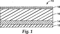
本発明の多層センサーフィルムの全体的な図を図1に示す。一般に、代表的な多層フィルムセンサー10は、(場合による)基材層12、反射層14、検出層16、および半反射層18を含む。
A general view of the multilayer sensor film of the present invention is shown in FIG. In general, a typical
本発明のセンサーフィルムは、検体または検体混合物の存在および/または濃度を検出するために使用することができる。検体は、気体(たとえば、蒸気)または液体であってよい。検体は分子、高分子、生体分子、または生体高分子であってよい。検体は、気体媒体(空気など)中または液体媒体(水または他の流体など)中に存在することができる。典型的には、検体は有機材料である。 The sensor film of the present invention can be used to detect the presence and / or concentration of an analyte or analyte mixture. The analyte may be a gas (eg, vapor) or a liquid. The analyte may be a molecule, polymer, biomolecule, or biopolymer. The analyte can be in a gaseous medium (such as air) or a liquid medium (such as water or other fluid). Typically, the analyte is an organic material.
少なくとも1つの実施態様において、検体に曝露したときに検出層を構成するポリマーの光学的厚さの変化によって、検体が検出される。検体は、半反射層の外側を通過して、検出層の光学的厚さを変化させる。一実施態様において、検体は、検出層の少なくとも一部の中に吸収される。吸収されることによって、色が変化して(多くの場合鮮明に)、検体の存在を示すことができる。 In at least one embodiment, the analyte is detected by a change in the optical thickness of the polymer comprising the detection layer when exposed to the analyte. The analyte passes outside the semi-reflective layer and changes the optical thickness of the detection layer. In one embodiment, the analyte is absorbed into at least a portion of the detection layer. By being absorbed, the color can change (in many cases vividly) to indicate the presence of the analyte.
光学的厚さの変化は、典型的には可視光範囲で観察可能であり、人の肉眼によって検出することができる。しかし、UV、赤外、または近赤外などの他の光源を照射した場合に、光学的厚さの変化を示すようにセンサーを設計することができる。種々の検出機構を使用することができる。好適な検出機構の例としては、分光光度計、光ファイバー分光光度計、および光検出器、たとえば、電荷結合素子(ccd)、デジタルカメラなどが挙げられる。 The change in optical thickness is typically observable in the visible light range and can be detected by the human eye. However, the sensor can be designed to show a change in optical thickness when illuminated by other light sources such as UV, infrared, or near infrared. Various detection mechanisms can be used. Examples of suitable detection mechanisms include spectrophotometers, fiber optic spectrophotometers, and photodetectors such as charge coupled devices (ccd), digital cameras, and the like.
別の実施態様においては、検体が存在すると隣接層から検出層が剥離するときに、検体が検出される。典型的には、検出層および隣接層の界面を検体が濡らすことによって界面接着力が低下する場合に、層間剥離が生じる。層間剥離が起こると、光学干渉がなくなり、センサーは知覚できる色を消失する。検体の存在は、検出層の内部の1種類以上のポリマーが隣接層からディウェッティングを引き起こす場合もある。隣接層との界面領域が減少する検出層の形状変化を伴うこの方法は、センサーフィルムの光学的性質を永続的に変化させる材料の内部で欠陥が生じる。 In another embodiment, the analyte is detected when the detection layer peels from the adjacent layer in the presence of the analyte. Typically, delamination occurs when the interfacial adhesion decreases as the analyte wets the interface between the detection layer and the adjacent layer. When delamination occurs, there is no optical interference and the sensor loses its perceivable color. The presence of the analyte may cause one or more polymers inside the detection layer to cause dewetting from adjacent layers. This method, which involves a change in the shape of the detection layer where the interfacial area with the adjacent layer is reduced, results in defects within the material that permanently change the optical properties of the sensor film.
基材
基材は場合により使用されるが、存在する場合、基材は、比色センサーを支持することができるあらゆる好適な材料を含むことができる。基材は、可撓性の場合も非可撓性の場合もある。用途に合わせて基材材料を調整することができる。好ましくは、真空蒸着において使用できると好適である。
Substrate A substrate is optionally used, but when present, the substrate can comprise any suitable material capable of supporting a colorimetric sensor. The substrate may be flexible or inflexible. The base material can be adjusted according to the application. Preferably, it can be used in vacuum deposition.
反射層
反射層は、全反射層または半反射層を形成可能なあらゆる材料を含むことができる。約20〜約200nmの厚さにおいて材料が全反射性となることが好ましい。より薄い層は、典型的には半反射反射層の作製に使用することができる。反射層は典型的には半反射層よりも反射性が高くなるように作製されるが、反射層および半反射層の反射性が同じあることが望ましい場合があり、その場合には、検体の存在に対する応答をセンサーフィルムのいずれの側からも見ることができる。
Reflective layer The reflective layer can comprise any material capable of forming a total reflective or semi-reflective layer. Preferably, the material is totally reflective at a thickness of about 20 to about 200 nm. Thinner layers can typically be used to make a semi-reflective reflective layer. The reflective layer is typically made to be more reflective than the semi-reflective layer, but it may be desirable for the reflective layer and the semi-reflective layer to have the same reflectivity, in which case the analyte The response to presence can be seen from either side of the sensor film.
反射層に好適な材料としては、アルミニウム、クロム、金、ニッケル、ケイ素、および銀などの金属または半金属が挙げられる。反射層中に含めることができる他の好適な材料としては、酸化クロムおよび酸化チタンなどの金属酸化物が挙げられる。 Suitable materials for the reflective layer include metals or metalloids such as aluminum, chromium, gold, nickel, silicon, and silver. Other suitable materials that can be included in the reflective layer include metal oxides such as chromium oxide and titanium oxide.
本発明のある代表的な実施態様においては、反射層は少なくとも約90%の反射性(すなわち、少なくとも約10%の透過性)であり、ある実施態様においては、約99%の反射性(すなわち、約1%の透過性)である。本発明の別の代表的な実施態様においては、反射層が半反射層であり、この反射層は少なくとも約20%の反射性であり、たとえば約20〜約90%の反射性、または約30〜約70%の反射性である。 In certain exemplary embodiments of the invention, the reflective layer is at least about 90% reflective (ie, at least about 10% transmissive), and in some embodiments, about 99% reflective (ie, , About 1% permeability). In another exemplary embodiment of the present invention, the reflective layer is a semi-reflective layer, and the reflective layer is at least about 20% reflective, such as about 20 to about 90% reflective, or about 30. ~ 70% reflective.
ある実施態様においては、反射層は、センサーを支持する基材としても機能する。反射層は、ほぼ連続の層または不連続層であってよい。さらに、反射層は1つ以上の反射層で構成されてよい。望ましくは、反射層は1つの反射層で構成される。 In some embodiments, the reflective layer also functions as a substrate that supports the sensor. The reflective layer may be a substantially continuous layer or a discontinuous layer. Further, the reflective layer may be composed of one or more reflective layers. Desirably, the reflective layer is composed of one reflective layer.
検出層
検出層は、1種類以上のポリマーまたはコポリマーを含むことができる。ほとんどの実施態様においては、検出層は、検体に曝露すると光学的厚さが変化する少なくとも1種類のポリマーを含む。光学的厚さの変化は、膨潤または収縮によるポリマーの物理的厚さの変化などの寸法変化によって、あるいは検体の存在または化学反応による検出層の屈折率の変化によって生じうる。検出層は、ある色から別の色に変化する場合があるし、ある色から無色に変化する場合もあるし、無色からある色に変化する場合もある。
Detection layer The detection layer can comprise one or more polymers or copolymers. In most embodiments, the detection layer comprises at least one polymer that changes optical thickness upon exposure to the analyte. The change in optical thickness can be caused by dimensional changes such as changes in the physical thickness of the polymer due to swelling or shrinkage, or by changes in the refractive index of the detection layer due to the presence of an analyte or chemical reaction. The detection layer may change from one color to another, may change from one color to colorless, or may change from colorless to a certain color.
反射層と同様に、検出層も1つ以上の層を含むことができる。検出層は、2つ以上の副層を含むこともできる。1つ以上の副層は不連続であったりパターンを有したりすることができる。副層は、典型的には異なるポリマー材料を含み、異なる検体を吸収することができる、および/または1種類以上の検体に対して異なる感度を有することができる。副層は、種々の構成を有することができる。たとえば、副層を積み重ねて2つ以上の層のスタックを形成することができるし、同じ層の中で隣接した構成で配置することもできる。 Similar to the reflective layer, the detection layer can include one or more layers. The detection layer can also include two or more sublayers. One or more sublayers can be discontinuous or have a pattern. Sublayers typically include different polymeric materials, can absorb different analytes, and / or have different sensitivities to one or more analytes. The sublayer can have various configurations. For example, the sub-layers can be stacked to form a stack of two or more layers, or can be arranged in an adjacent configuration in the same layer.
検出層は、検体に曝露することによって有色の画像、単語、またはメッセージを形成するように、検出層があるパターンを含むことができる。特定の検体に対して反応性である1つ以上の部分と、同じ検体に対して非反応性である1つ以上の部分とを有することによって、副層にパターンを形成することができる。または、反応性材料のパターンを、より大きな非反応性副層の上に付着させることもできる。この場合、検体が吸収されるまでは、光学的厚さの差が分からないように、パターン形成された層を非常に薄くすることが好ましい。このパターン形成によって、検体に曝露した場合に使用者が容易に確認可能な警告を提供することができる。 The detection layer can include a pattern with the detection layer such that exposure to the analyte forms a colored image, word, or message. By having one or more portions that are reactive to a particular analyte and one or more portions that are non-reactive to the same analyte, a pattern can be formed in the sublayer. Alternatively, a pattern of reactive material can be deposited on a larger non-reactive sublayer. In this case, it is preferable to make the patterned layer very thin until the specimen is absorbed so that the difference in optical thickness is not known. This pattern formation can provide a warning that can be easily confirmed by the user when exposed to the specimen.
米国特許第6,010,751号明細書に記載されるようにして、検出層の厚さにパターンを形成することができる。このことは、検体の存在によって検出層の膨潤または収縮が起こり、それによってパターンが消失する(たとえば、薄い部分が膨潤して厚い部分と同じ厚さになる場合)またはパターンが現れる(たとえば、特定の部分が収縮して、隣接する部分よりも厚くなる)ようにセンサーが設計されるときには望ましい場合がある。最初に同じ色に見える薄い領域と厚い領域とから始まり、1種類以上の検体に曝露すると、薄い領域および厚い領域の一方または両方が膨潤して、2つの異なる色相が生じることによってパターンが見えるようにすることもできる。 A pattern can be formed in the thickness of the detection layer as described in US Pat. No. 6,010,751. This is due to the presence or absence of the analyte causing the detection layer to swell or contract, thereby causing the pattern to disappear (eg, when the thin part swells to the same thickness as the thick part) or the pattern appears (eg, specific May be desirable when the sensor is designed such that the portion of the sensor shrinks and becomes thicker than the adjacent portion. Beginning with thin and thick areas that initially appear the same color, exposure to one or more analytes will cause one or both of the thin and thick areas to swell, resulting in two different hues to make the pattern visible It can also be.
検出層は、ポリマー成分のブレンドを含むことができる。このブレンドは均一であっても不均一であってもよい。検出層中のポリマー成分のブレンドによって、比較的小さなセンサーを使用して、多数の検体を検出できるようになる。本発明の代表的な一実施態様においては、検出層は、少なくとも2種類の異なるポリマー成分を含み、これらのポリマー成分は、(1)互いにブレンドされている、(2)特定の1つの層中に存在するが互いにブレンドされていない(すなわち隣接する構成)、(3)互いに別の層中に存在する(すなわち1つのスタック中にある)、または(4)(1)から(3)のいずれかの組み合わせである。 The detection layer can include a blend of polymer components. This blend may be uniform or non-uniform. The blend of polymer components in the detection layer allows a large number of analytes to be detected using a relatively small sensor. In one exemplary embodiment of the present invention, the detection layer comprises at least two different polymer components that are (1) blended together, (2) in one particular layer. Present but not blended with each other (ie, adjacent configurations), (3) present in different layers of each other (ie, in one stack), or (4) any of (1) through (3) It is a combination.
検出層は多孔質であってもよい。言い換えると、検出層は、その体積全体に細孔の連続網目構造を有することができる。これによって、検体に曝露する表面積が増加し、および/または蒸気状の検体を凝縮させる細孔の性質のために、検出感度を増大させることができる。多孔性は、国際公開第01/21693号パンフレットに記載されるものなどの高分散相エマルジョンから製造されるフォームなどの多孔質材料を使用して検出層を形成することによって得ることができる。多孔性は、二酸化炭素による発泡により共連続ナノポーラス材料を形成することによって(“Macromolecules”,2001,vol.34、pp.8792〜8801参照)、またはポリマーブレンドのナノ層分離によって(“Science”,1999,vol.283、p.520参照)得ることもできる。一般に、細孔径は、検出方法に使用される光源の波長よりも小さいことが必要である。典型的には、10nm以下の平均孔径を有する細孔が検出層中には望ましい。 The detection layer may be porous. In other words, the detection layer can have a continuous network of pores throughout its volume. This can increase the surface area exposed to the analyte and / or increase the detection sensitivity due to the nature of the pores that condense the vaporous analyte. The porosity can be obtained by forming the detection layer using a porous material such as a foam made from a highly dispersed phase emulsion such as that described in WO 01/21693. Porosity can be achieved by forming a co-continuous nanoporous material by foaming with carbon dioxide (see “Macromolecules”, 2001, vol. 34, pp. 8792-8801) or by nanolayer separation of polymer blends (“Science”, 1999, vol.283, p.520). In general, the pore diameter needs to be smaller than the wavelength of the light source used in the detection method. Typically, pores having an average pore size of 10 nm or less are desirable in the detection layer.
本発明の一実施態様において、固有の微孔性を有するポリマー(polymer having an intrinsic microporosity)、すなわちPIMを検出層の形成に使用することもできる。本明細書において使用される場合、「固有の微孔性を有するポリマー」または「PIM」は、非常に剛直でゆがんだ分子構造のために微孔性固体を形成する非網状ポリマーを意味する。このような分子構造のために、PIMは空間を効率的に充填することができず、そのために微孔性構造が得られる(たとえば、典型的には約2nm未満の平均孔径を有する細孔を含有する構造)。好適な固有の微孔性のポリマー(PIM)としては、限定するものではないが、「固有の微孔性のポリマー(PIM):堅牢で、溶液加工可能な有機ナノポーラス材料」(Polymers of intrinsic microporosity (PIMs):robust,solution−processable,organic nanoporous materials),バッド(Budd)ら,Chem.Commun.,2004,pp.230〜231に開示されるポリマーが挙げられ、この主題全体が本明細書に援用される。 In one embodiment of the invention, a polymer having an intrinsic microporosity, i.e. PIM, can also be used to form the detection layer. As used herein, “polymer with intrinsic microporosity” or “PIM” means a non-reticulated polymer that forms a microporous solid due to a very rigid and distorted molecular structure. Due to such molecular structure, the PIM cannot efficiently fill the space, thereby resulting in a microporous structure (eg, pores having an average pore size typically less than about 2 nm). Containing structure). Suitable intrinsic microporous polymers (PIMs) include, but are not limited to, “intrinsic microporous polymers (PIMs): robust, solution processable organic nanoporous materials” (Polymers of intrinsic microporosity). (PIMs): robust, solution-processable, organic nanomaterials), Budd et al., Chem. Commun. , 2004, pp. And the polymers disclosed in 230-231, the entire subject matter of which is hereby incorporated by reference.
検出層中の1種類以上のポリマーは少なくとも部分的に架橋していてもよい。機械的安定性およびある種の検体に対する感度が増加する場合があるので、ある実施態様においては架橋が望ましい場合もある。架橋は、1種類以上の多官能性モノマーを検出層中に組み込むことによって、あるいはたとえば、電子ビームまたはガンマ線による処理などを検出層に対して実施することによって実現することができる。本発明の望ましい一実施態様においては、ポロゲンの存在下で架橋が実施され、後にこのポロゲンを架橋系から抽出して、多孔質検出層を形成することができる。好適なポロゲンとしては、直鎖アルカン(たとえば、デカン)または芳香族(たとえば、ベンゼン、トルエン)などの不活性有機分子が挙げられるが、これらに限定されるものではない。 One or more types of polymers in the detection layer may be at least partially crosslinked. In some embodiments, crosslinking may be desirable because mechanical stability and sensitivity to certain analytes may be increased. Crosslinking can be achieved by incorporating one or more multifunctional monomers into the detection layer, or by carrying out treatment with the detection layer, for example, by electron beam or gamma radiation. In a preferred embodiment of the present invention, crosslinking is performed in the presence of a porogen, which can then be extracted from the crosslinking system to form a porous detection layer. Suitable porogens include, but are not limited to, inert organic molecules such as linear alkanes (eg, decane) or aromatics (eg, benzene, toluene).
多くの用途においては、ポリマーまたはコポリマーが疎水性であることが望ましい。これによって、水蒸気(または液体の水)が、ポリマーの光学的厚さを変化させ、検体の検出、たとえば有機溶媒蒸気の検出を妨害する可能性が軽減される。 In many applications it is desirable for the polymer or copolymer to be hydrophobic. This reduces the possibility that water vapor (or liquid water) will change the optical thickness of the polymer and interfere with analyte detection, such as organic solvent vapor detection.
有機溶媒蒸気の検出の場合、検出層に好適なポリマー材料としては、疎水性のアクリレートおよびメタクリレート、二官能性モノマー、ビニルモノマー、炭化水素モノマー(オレフィン)、シランモノマー、ならびにフッ素化モノマーなどの種類のモノマーから調製されるポリマーおよびコポリマー(ブロックコポリマーを含む)が挙げられるが、これらに限定されるものではない。 For organic solvent vapor detection, suitable polymer materials for the detection layer include hydrophobic acrylates and methacrylates, bifunctional monomers, vinyl monomers, hydrocarbon monomers (olefins), silane monomers, and fluorinated monomers. Polymers and copolymers (including block copolymers) prepared from these monomers include, but are not limited to:
疎水性のアクリレートおよびメタクリレートの例としては、アルキル基−CxH2xCH3(式中、xは1〜約17である)を有するn−アルキル(メタ)アクリレート、メチル(メタ)アクリレート、イソデシル(メタ)アクリレート、2−エチルヘキシル(メタ)アクリレート、シクロヘキシル(メタ)アクリレート、n−デシル(メタ)アクリレート、n−ブチル(メタ)アクリレート、イソオクチル(メタ)アクリレート、イソプロピル(メタ)アクリレート、ラウリル(メタ)アクリレート、エチル(メタ)アクリレート、アダマンチル(メタ)アクリレート、t−ブチル(メタ)アクリレート、2−フェノキシエチル(メタ)アクリレート、イソボルニル(メタ)アクリレート、およびポリ(ジメチルシロキサン)モノ(メタ)アクリレートが挙げられるが、これらに限定されるものではない。 Examples of hydrophobic acrylates and methacrylates include n-alkyl (meth) acrylates, methyl (meth) acrylates, isodecyl having an alkyl group —C x H 2x CH 3 , where x is from 1 to about 17. (Meth) acrylate, 2-ethylhexyl (meth) acrylate, cyclohexyl (meth) acrylate, n-decyl (meth) acrylate, n-butyl (meth) acrylate, isooctyl (meth) acrylate, isopropyl (meth) acrylate, lauryl (meth) ) Acrylate, ethyl (meth) acrylate, adamantyl (meth) acrylate, t-butyl (meth) acrylate, 2-phenoxyethyl (meth) acrylate, isobornyl (meth) acrylate, and poly (dimethylsiloxane) mono (meth) a Examples include, but are not limited to, acrylate.
多官能性モノマーの例としては、ジビニルベンゼン、エチレングリコールジ(メタ)アクリレート、ジエチレングリコールジ(メタ)アクリレート、トリエチレングリコールジ(メタ)アクリレート、テトラエチレングリコールジ(メタ)アクリレート、トリプロピレングリコールジ(メタ)アクリレート、ポリエチレングリコールジ(メタ)アクリレート 1,6−ヘキサンジオールジ(メタ)アクリレート、トリメチロールプロパンジ(メタ)アクリレート、ネオペンチルグリコールジ(メタ)アクリレート、N,N−メチレンビス(メタ)アクリルアミド、ポリ(ジメチルシロキサン)ジ(メタ)アクリレート、ポリ(エチレングリコール)ジ(メタ)アクリレート、UCBケミカルズ(UCB Chemicals)より商品名「IRR 214」で市販されるものなどのジアクリレート、ペンタエリスリトールトリ−およびテトラ−アクリレート、ならびにトリメチロールプロパントリ(メタ)アクリレートが挙げられるが、これらに限定されるものではない。 Examples of multifunctional monomers include divinylbenzene, ethylene glycol di (meth) acrylate, diethylene glycol di (meth) acrylate, triethylene glycol di (meth) acrylate, tetraethylene glycol di (meth) acrylate, tripropylene glycol di ( (Meth) acrylate, polyethylene glycol di (meth) acrylate 1,6-hexanediol di (meth) acrylate, trimethylolpropane di (meth) acrylate, neopentyl glycol di (meth) acrylate, N, N-methylenebis (meth) acrylamide , Poly (dimethylsiloxane) di (meth) acrylate, poly (ethylene glycol) di (meth) acrylate, trade name “UCB Chemicals” Examples include, but are not limited to, diacrylates such as those commercially available at R 214 ", pentaerythritol tri- and tetra-acrylate, and trimethylolpropane tri (meth) acrylate.
ビニルモノマーの例としては、スチレン、α−メチルスチレン、ビニルアセテート、ビニルブチレート、ビニルステアレート、ビニルクロリド、およびビニルノルボルネンが挙げられるが、これらに限定されるものではない。 Examples of vinyl monomers include, but are not limited to, styrene, α-methylstyrene, vinyl acetate, vinyl butyrate, vinyl stearate, vinyl chloride, and vinyl norbornene.
炭化水素モノマー(オレフィン)の例としては、イソブチレン、エチレン、プロピレン、ブタジエン、およびノルボルネンが挙げられるが、これらに限定されるものではない。 Examples of hydrocarbon monomers (olefins) include, but are not limited to, isobutylene, ethylene, propylene, butadiene, and norbornene.
シランモノマーの例としては、オルガノヒドロシラン、アルコキシシラン、フェノキシシラン、およびフルオロアルコキシシランが挙げられるが、これらに限定されるものではない。 Examples of silane monomers include, but are not limited to, organohydrosilanes, alkoxysilanes, phenoxysilanes, and fluoroalkoxysilanes.
フッ素化モノマーの例としては、テトラフルオロエチレン、フッ化ビニリデン、ヘキサフルオロプロピレン、およびパーフルオロアルキル(メタ)アクリレートが挙げられるが、これらに限定されるものではない。 Examples of fluorinated monomers include, but are not limited to, tetrafluoroethylene, vinylidene fluoride, hexafluoropropylene, and perfluoroalkyl (meth) acrylate.
溶液中の検出、極性の高い検体の検出、および/またはセンサーアレイにおける使用の場合、検出層に好適なポリマー材料としては、ヒドロキシル化モノマー、アクリルアミド、無水物、アルデヒド官能化モノマー、アミンまたはアミン塩で官能化されたモノマー、酸官能化モノマー、エポキシド官能化モノマー、ビニルモノマー、前述の多官能性モノマーなどの種類のモノマーから調製されるポリマーおよびコポリマー(ブロックコポリマーを含む)、ならびにその他のポリマーが挙げられるが、これらに限定されるものではない。 For detection in solution, detection of highly polar analytes, and / or use in sensor arrays, suitable polymeric materials for the detection layer include hydroxylated monomers, acrylamides, anhydrides, aldehyde functionalized monomers, amines or amine salts Monomers and acid-functionalized monomers, epoxide-functionalized monomers, vinyl monomers, polymers and copolymers prepared from types of monomers such as the aforementioned multifunctional monomers (including block copolymers), and other polymers Although it is mentioned, it is not limited to these.
ヒドロキシル化モノマーの例としては、ヒドロキシアルキル(メタ)アクリレート、ヒドロキシエチル(メタ)アクリレート、およびヒドロキシメチル(メタ)アクリレート挙げられるが、これらに限定されるものではない。 Examples of hydroxylated monomers include, but are not limited to, hydroxyalkyl (meth) acrylates, hydroxyethyl (meth) acrylates, and hydroxymethyl (meth) acrylates.
アクリルアミドおよびアクリロニトリルの例としては、(メタ)アクリルアミド、N−イソプロピル(メタ)アクリルアミド、N,N−ジメチル(メタ)アクリルアミド、および(メタ)アクリロニトリルが挙げられるが、これらに限定されるものではない。 Examples of acrylamide and acrylonitrile include, but are not limited to, (meth) acrylamide, N-isopropyl (meth) acrylamide, N, N-dimethyl (meth) acrylamide, and (meth) acrylonitrile.
無水物の例としては、無水(メタ)アクリル酸および無水マレイン酸が挙げられるが、これらに限定されるものではない。 Examples of anhydrides include, but are not limited to, (meth) acrylic anhydride and maleic anhydride.
アルデヒド官能化モノマーの例としてはアクロレインが挙げられるが、これに限定されるものではない。 An example of an aldehyde functionalized monomer includes, but is not limited to, acrolein.
アミンまたはアミン塩で官能化されたモノマーとしては、t−ブチルアミノエチル(メタ)アクリレート、ジイソプロピルアミノエチル(メタ)アクリレート、ジメチルアミノエチル(メタ)アクリレート、ビニルピリジン、ジメチルアミノエチル(メタ)アクリレート−メチル塩化物塩、アミノスチレン、4−アミノスチレン、およびビニルイミダゾールが挙げられるが、これらに限定されるものではない。 Monomers functionalized with amines or amine salts include t-butylaminoethyl (meth) acrylate, diisopropylaminoethyl (meth) acrylate, dimethylaminoethyl (meth) acrylate, vinylpyridine, dimethylaminoethyl (meth) acrylate— Examples include, but are not limited to, methyl chloride salts, aminostyrene, 4-aminostyrene, and vinylimidazole.
酸官能化モノマーの例としては、(メタ)アクリル酸、カルボキシエチル(メタ)アクリレート、(メタ)アクリル酸金属塩、スチレンスルホン酸、UCBケミカルズ(UCB Chemicals)より商品名「エベクリル170」(EBECRYL 170)でUCBケミカルズ(UCB Chemicals)より市販されるモノマー、ビニルホスホン酸、およびビニルスルホン酸が挙げられるが、これらに限定されるものではない。 Examples of acid functionalized monomers include (meth) acrylic acid, carboxyethyl (meth) acrylate, (meth) acrylic acid metal salt, styrene sulfonic acid, UCB Chemicals, and trade name “Evecryl 170”. ), But are not limited to monomers, vinyl phosphonic acid, and vinyl sulfonic acid commercially available from UCB Chemicals.
エポキシド官能化モノマーの例としては、グリシジル(メタ)アクリレートが挙げられるが、これに限定されるものではない。 Examples of epoxide functionalized monomers include, but are not limited to, glycidyl (meth) acrylate.
ビニルモノマーの例としては、N−ビニルピロリドン、ビニルジメチルアザラクトン(VDM)、塩化ビニリデン、ビニルアルコール、およびビニルフェノールが挙げられるが、これに限定されるものではない。 Examples of vinyl monomers include, but are not limited to, N-vinyl pyrrolidone, vinyl dimethylazalactone (VDM), vinylidene chloride, vinyl alcohol, and vinyl phenol.
他のポリマーの例としては、ポリ(エチレンオキシド)、ポリ(カプロラクトン)、ポリ(スルホン)、ポリ(エチレングリコール)、ポリ(ウレタン)、ポリ(カーボネート)、ポリ(エチレンイミン)、ポリ(ビニルアルコール)、ポリ(ビニルフェノール)、エチルセルロース、フルオロポリオール、ポリエステル、ポリアミド、ポリイミド、およびポリアセタールが挙げられるが、これらに限定されるものではない。検出層のポリマー成分は、特定の検体を検出するために組み込まれた適切な官能基または分子受容体を有することもできる。たとえば、ポリ(アクリル酸)などの酸官能化ポリマーは、アンモニアガスなどの有機塩基を検出することができる。金属ポルフィリンなどの金属錯体を検出層中に組み込むことによって、ホスフィンまたはメルカプタンなどの配位種を検出することができる。好適な分子受容体としては、カリックスアレーン、シクロデキストリン、樹枝状ポリマー、カーボンナノチューブ、アザクラウン、クラウンエーテル、ルイス酸官能性を有する陰イオンキレート剤、有機金属金属錯体、ポルフィリン、金属ポルフィリン、ペプチド、グリコペプチド、タンパク質、抗体、酵素、オリゴヌクレオチド、および核酸が挙げられるが、これらに限定されるものではない。 Examples of other polymers include poly (ethylene oxide), poly (caprolactone), poly (sulfone), poly (ethylene glycol), poly (urethane), poly (carbonate), poly (ethyleneimine), poly (vinyl alcohol) , Poly (vinylphenol), ethylcellulose, fluoropolyol, polyester, polyamide, polyimide, and polyacetal, but are not limited thereto. The polymer component of the detection layer can also have suitable functional groups or molecular receptors incorporated to detect a particular analyte. For example, acid functionalized polymers such as poly (acrylic acid) can detect organic bases such as ammonia gas. By incorporating a metal complex such as a metal porphyrin into the detection layer, a coordination species such as phosphine or mercaptan can be detected. Suitable molecular receptors include calixarenes, cyclodextrins, dendritic polymers, carbon nanotubes, azacrowns, crown ethers, anion chelators with Lewis acid functionality, organometallic metal complexes, porphyrins, metalloporphyrins, peptides, Examples include, but are not limited to, glycopeptides, proteins, antibodies, enzymes, oligonucleotides, and nucleic acids.
本発明のさらなる実施態様においては、検出層は、1種類以上の無機材料を単独で含む、または1種類以上の上述のポリマー材料とともに含む。本発明の代表的な一実施態様においては、検出層は、1種類以上の無機材料を含むが、ポリマー材料は含まない。さらなる代表的な実施態様においては、検出層は、1種類以上の無機材料と、前述の1種類以上のポリマー材料とを含む。無機材料およびポリマー材料の両方を含有する実施態様においては、無機材料は、検出層中の別の層として存在することができるし、ポリマー材料と混合して単層を形成することもできる。さらに、無機材料は、検出層中で1つ以上のポリマー層とは分離した別の層として存在することができるし(すなわち、ポリマー層と無機層とのスタック)、ポリマー材料とともに単層中に存在するが、ポリマー材料とは混合されていなくてもよい(すなわち、無機材料の明確な区画と、ポリマー材料の明確な区画とを有する並列構造)。 In a further embodiment of the invention, the detection layer comprises one or more inorganic materials alone or together with one or more of the aforementioned polymer materials. In one exemplary embodiment of the present invention, the detection layer comprises one or more inorganic materials but no polymer material. In a further exemplary embodiment, the detection layer comprises one or more inorganic materials and one or more polymer materials as described above. In embodiments containing both inorganic and polymeric materials, the inorganic material can be present as a separate layer in the detection layer or can be mixed with the polymeric material to form a monolayer. Furthermore, the inorganic material can be present in the detection layer as a separate layer that is separate from one or more polymer layers (ie, a stack of polymer and inorganic layers), and together with the polymer material in a single layer. Although present, it may not be mixed with the polymeric material (ie, a side-by-side structure with distinct compartments of inorganic material and distinct compartments of polymer material).
検出層中に使用される好適な無機材料としては、光学干渉によって発色するのに適切な厚さの透明で多孔質の金属酸化物、窒化物、酸窒化物が挙げられるが、これらに限定されるものではない。好適な無機材料の具体例としては、酸化ケイ素、窒化ケイ素、酸窒化ケイ素、酸化アルミニウム、酸化チタン、窒化チタン、酸窒化チタン、酸化スズ、酸化ジルコニウム、およびそれらの組み合わせが挙げられるが、これらに限定されるものではない。ゼオライトなどの他の無機材料も、検出層中への使用に好適である。望ましくは、無機材料が、前述の定義の多孔質材料である。 Suitable inorganic materials for use in the detection layer include, but are not limited to, transparent and porous metal oxides, nitrides, and oxynitrides of appropriate thickness to develop color by optical interference. It is not something. Specific examples of suitable inorganic materials include silicon oxide, silicon nitride, silicon oxynitride, aluminum oxide, titanium oxide, titanium nitride, titanium oxynitride, tin oxide, zirconium oxide, and combinations thereof. It is not limited. Other inorganic materials such as zeolite are also suitable for use in the detection layer. Desirably, the inorganic material is a porous material as defined above.
本発明の一実施態様においては、検出層中の「検体収着性材料」または「検体反応性材料」として無機材料が使用される。この実施態様において、前述のような無機材料は、単独で使用することができるし、検体反応性または検体収着性基が結合したベース基材として使用することもできる。たとえば、オルガノシラン化合物が結合した粒子状の金属酸化物、窒化物、および/または酸窒化物を検出層全体に分散させることができる。 In one embodiment of the present invention, an inorganic material is used as the “analyte sorbing material” or “analyte reactive material” in the detection layer. In this embodiment, the inorganic material as described above can be used alone or as a base substrate to which an analyte reactive or analyte sorbing group is bound. For example, particulate metal oxide, nitride, and / or oxynitride to which an organosilane compound is bonded can be dispersed throughout the detection layer.
適切な化合物および/または検体受容体部分を検出層中に組み込むことによって、溶液中の広範囲の検体のセンサーを形成可能となる。最初に付着させるか、または付着させた材料を後に官能化するかのいずれかによって、ペプチドまたは抗体などの受容体分子を場合により上記ポリマーと共有結合させることができる。細菌、タンパク質、イオンなどを選択的に検出するためのバイオセンサーを製造することができる。 Incorporation of appropriate compounds and / or analyte receptor moieties into the detection layer allows the formation of sensors for a wide range of analytes in solution. Receptor molecules such as peptides or antibodies can optionally be covalently attached to the polymer, either by first attaching or by subsequently functionalizing the attached material. Biosensors for selectively detecting bacteria, proteins, ions, etc. can be manufactured.
検出層は、あらゆる所望の全体厚さを有することができる。望ましくは、検出層は、約50nmを超える、たとえば約100〜約1000nmの範囲の全体厚さを有する。本発明の一実施態様においては、検出層は、検出層全体でほぼ同じ層厚さを有する。たとえば、図1の検出層16を参照されたい。本発明の別の実施態様においては、検出層は、検出層中の第1の位置と、検出層中の1つ以上の他の位置とで異なる層厚さを有する。いずれの場合も、検出層の上に適用される半反射層は、検出層の厚さのばらつきに適合するように適用することができる。
The detection layer can have any desired overall thickness. Desirably, the detection layer has an overall thickness of greater than about 50 nm, such as in the range of about 100 to about 1000 nm. In one embodiment of the invention, the detection layer has substantially the same layer thickness throughout the detection layer. See, for example, the
ある位置と別の位置で厚さが異なる検出層を有する本発明の代表的なセンサーを図2に示す。図2に示されるように、センサー20は、(場合による)基材層22、反射層24、検出層26、および半反射層28を含む。検出層26は、第1の位置26aにおいて第1の厚さt26a、第2の位置26bにおいて第2の厚さt26b、第3の位置26cにおいてにおいて第3の厚さt26cを有する。代表的なセンサー20において、検出層26の層厚さは検出層26全体で変動しているが、半反射層28の厚さはほぼ一定に維持されている。
FIG. 2 shows a typical sensor of the present invention having a detection layer having a thickness different from one position to another. As shown in FIG. 2, the
本発明の代表的な一実施態様においては、検出層は、検出層中に配置された1つ以上の「ウェル」を含む。本明細書において使用される場合、用語「ウェル」は、検出層中の孔、溝、チャネル、またはその他のあらゆる空隙(細孔以外)を表すために使用される。細孔とは異なり、検出層の体積全体でウェルは連続網目構造を形成していない。典型的には、ウェルは、検出層の上面(すなわち半反射層の下)から、検出層中の所定の深さまで延在している。ウェルは、典型的には約10nm未満の少なくとも1つの寸法(すなわち、長さ、幅、または直径)を有するが、しかし、本発明においてあらゆるウェルの大きさを使用することができる。本発明の望ましい一実施態様においては、ウェルの少なくとも1つの寸法(すなわち、長さ、幅、または直径)が約1.0〜約10nmの範囲であり、より望ましくは約5nmである。本発明のある実施態様においては、ウェルの少なくとも1つの寸法(たとえば、幅)が約1.0〜約10nmの範囲であり、少なくとも1つの別の寸法(たとえば、長さ)が5nmをはるかに超え、たとえばその寸法は10nmを超えて検出層の幅までの範囲である。検出層内にウェルを有する本発明の代表的なセンサーを図3に示す。 In one exemplary embodiment of the present invention, the detection layer includes one or more “wells” disposed in the detection layer. As used herein, the term “well” is used to represent a hole, groove, channel, or any other void (other than a pore) in the detection layer. Unlike the pores, the well does not form a continuous network throughout the volume of the detection layer. Typically, the well extends from the top surface of the detection layer (ie, below the semi-reflective layer) to a predetermined depth in the detection layer. Wells typically have at least one dimension (ie, length, width, or diameter) of less than about 10 nm, however, any well size can be used in the present invention. In a preferred embodiment of the present invention, at least one dimension (i.e., length, width, or diameter) of the well is in the range of about 1.0 to about 10 nm, and more desirably about 5 nm. In certain embodiments of the invention, at least one dimension (eg, width) of the well is in the range of about 1.0 to about 10 nm, and at least one other dimension (eg, length) is much greater than 5 nm. For example, the dimension is in the range from more than 10 nm to the width of the detection layer. A representative sensor of the present invention having a well in the detection layer is shown in FIG.
図3に示されるように、代表的な多層フィルムセンサー30は、(場合による)基材層32と、反射層34と、ウェル37を有する検出層36と、検出層36およびウェル37の上にある半反射層38とを含む。この実施態様において、検出層36は、ウェル37の内面に沿った表面領域37aのために表面積が増加している。検出層36中の表面積の増加の程度は、一定面積当たりのウェル37の数、各ウェル37の深さ、および各ウェル37の容積の1つ以上の要因を変動させることによって制御することができる。
As shown in FIG. 3, a representative
ウェルが存在する場合、検出層中の不規則な空隙として存在する場合もあるし、検出層中に分散したパターンの形態である場合もあり、これらのウェルは、検出層中の所望の深さまで延在する。検出層が1つ以上のウェルを有する場合、そのウェルは種々の技術を使用して形成することができる。検出層中にウェルを形成するための好適な方法の1つは、後出の実施例10に記載されるようなエッチング方法である。この代表的な方法では、一時的または永続的な担体の上に最初に反射層がコーティングされる。次に、ポリマー検出層などの検出層を反射層の上にコーティングする。次に、Crなどの金属を、「島」の形態(すなわち、金属の島とコーティングされていない領域とのパターン)で検出層の上にコーティングする。検出層上の島の大きさおよび密度は、金属(すなわちCr)源と検出層との間にスクリーンを配置することによって制御することができる。次に、反応性イオンエッチング(RIE)方式において酸素プラズマを使用して、検出層のコーティングされていない領域をエッチングする。金属(たとえばCr)の島はエッチングマスクとして機能し、エッチングステップ中にCrOxなどの透明酸化物に転化する(たとえば、図3の層39参照)。
If wells are present, they may be present as irregular voids in the detection layer, or may be in the form of a pattern dispersed in the detection layer, these wells up to the desired depth in the detection layer Extend. If the detection layer has one or more wells, the wells can be formed using various techniques. One suitable method for forming a well in the detection layer is an etching method as described in Example 10 below. In this exemplary method, a reflective layer is first coated on a temporary or permanent carrier. Next, a detection layer such as a polymer detection layer is coated on the reflective layer. Next, a metal such as Cr is coated on the detection layer in the form of “islands” (ie, a pattern of metal islands and uncoated areas). The size and density of the islands on the detection layer can be controlled by placing a screen between the metal (ie, Cr) source and the detection layer. Next, an oxygen plasma is used in a reactive ion etching (RIE) method to etch an uncoated region of the detection layer. The metal (eg, Cr) island functions as an etch mask and is converted to a transparent oxide such as CrO x during the etch step (see, eg,
上述の代表的なエッチング方法によって、透明酸化物の島の間にナノメートルサイズのウェルが形成される。典型的には、透明酸化物の島は、検出層上面の上に均一に分散し、少なくとも1つの寸法(すなわち、長さ、幅、または直径)が約100nm未満となるが、あらゆる透明酸化物の島の大きさ、形状、および密度を本発明において使用することができる。 The typical etching method described above forms nanometer-sized wells between transparent oxide islands. Typically, the transparent oxide islands are uniformly distributed over the top surface of the detection layer and have at least one dimension (ie, length, width, or diameter) of less than about 100 nm, although any transparent oxide The size, shape, and density of the islands can be used in the present invention.
ウェル37は、所定の用途に望ましいあらゆる深さで検出層36中に延在することができる。図3に示されるように、ウェル37は、検出層36中に延在して、検出層36中のある点で終わることができる。別の実施態様においては、ウェル37は、検出層36を通過して反射層34まで延在することができる(図3参照)。
Well 37 can extend into
エッチングステップが終了してから、透明酸化物の島およびウェルの上に、図3に示す半透明層38などの半透明層(または他の層)をコーティングすることができる。この実施態様において、色ずれの干渉によって、特定の視野角とともに変化する1種類の均一な色の外観が得られる。または、検出層の「島」と、「島」の間のウェルとの上に半透明層を適用する前に、透明酸化物の島(すなわち、図3に示される層39)を除去することもできる。
After the etching step is completed, a translucent layer (or other layer) such as
半反射層
半反射層は、浸透性半反射層を形成することができるあらゆる材料を含むことができ、検出層とは異なる屈折率を有する。ほとんどの実施態様においては、この材料が約5nmの厚さで半反射性となることが好ましいが、その理由は、この厚さにおいてほとんどの検体が、この層を透過して検出層に到達することができるからである。望ましい厚さは、層の形成に使用される材料、検出するべき検体、および担体を有する媒体に依存する。
Semi-reflective layer The semi-reflective layer can comprise any material capable of forming a permeable semi-reflective layer and has a different refractive index than the detection layer. In most embodiments, it is preferred that this material be semi-reflective at a thickness of about 5 nm, because most analytes pass through this layer to reach the detection layer at this thickness. Because it can. The desired thickness depends on the material used to form the layer, the analyte to be detected, and the medium with the carrier.
好適な材料としては、アルミニウム、クロム、金、ニッケル、ケイ素、および銀などの金属および半金属が挙げられる。半反射層中に含めることができる他の好適な材料としては、酸化アルミニウム、酸化チタン、および酸化クロムなどの酸化物が挙げられる。 Suitable materials include metals and metalloids such as aluminum, chromium, gold, nickel, silicon, and silver. Other suitable materials that can be included in the semi-reflective layer include oxides such as aluminum oxide, titanium oxide, and chromium oxide.
反射層と同様に、半反射層もほぼ連続の層でも不連続層でもよい。さらに、反射層と同様に、半反射層も1つ以上の半反射層で構成されてよい。望ましくは、半反射層は、ほぼ連続または不連続のいずれかの1つの半反射層で構成される。 Similar to the reflective layer, the semi-reflective layer may be a substantially continuous layer or a discontinuous layer. Further, like the reflective layer, the semi-reflective layer may be composed of one or more semi-reflective layers. Desirably, the semi-reflective layer comprises one semi-reflective layer that is either substantially continuous or discontinuous.
本発明の代表的な一実施態様においては、半反射層は、ほぼ連続の層である。この実施態様において、半反射層の構造および組成は、半反射層の上面および全体にわたってほぼ均一であって良い。または、半反射層の構造および/または組成は、半反射層の上面および全体で変化してもよい。たとえば、半反射層の上面の第1の位置において特定の検体の検体浸透性が高くなり、上面の第2の位置において同じ検体の検体浸透性が低くなるように、半反射層の浸透性に差を持たせることができる。半反射層の上面の第1および第2の位置は、互いに不規則に配置することもできるし、上面上で特定のパターンを形成することもできる。 In an exemplary embodiment of the invention, the semi-reflective layer is a substantially continuous layer. In this embodiment, the structure and composition of the semi-reflective layer may be substantially uniform over the top surface and the entire semi-reflective layer. Alternatively, the structure and / or composition of the semi-reflective layer may vary on the top surface and the entire semi-reflective layer. For example, the permeability of the semi-reflective layer is such that the analyte permeability of a specific specimen is high at the first position on the upper surface of the semi-reflective layer and the analyte permeability of the same specimen is low at the second position on the upper surface. There can be a difference. The first and second positions on the upper surface of the semi-reflective layer can be arranged irregularly with each other, or a specific pattern can be formed on the upper surface.
ほぼ連続の半反射層は、半反射層の第1の領域が半反射層の第2の領域よりも光の反射率が高くなるパターンを有することもできる。半反射層上の第1および第2の領域は、半反射層の上面上または内部でパターンを形成することができる。前述のパターンが形成された検出層と同様に、パターンが形成された半反射層は、下にある検出層が検体に曝露したときに有色の画像、単語、またはメッセージを形成するようなパターンを含むことができる。この半反射層によって、検体に曝露した場合に使用者が容易に確認可能な警告を提供することができる。 The substantially continuous semi-reflective layer may have a pattern in which the first region of the semi-reflective layer has a higher light reflectance than the second region of the semi-reflective layer. The first and second regions on the semi-reflective layer can be patterned on or within the upper surface of the semi-reflective layer. Similar to the detection layer with the pattern described above, the patterned semi-reflective layer has a pattern that forms a colored image, word, or message when the underlying detection layer is exposed to the analyte. Can be included. This semi-reflective layer can provide a warning that can be easily confirmed by the user when exposed to the specimen.
あらゆる多数の方法を使用して、半反射層の浸透性を変化させ、および/または半反射層の上および内部にパターンを形成することができる。好適な方法としては、半反射層の堆積条件を空間的に制御して半反射層の厚さまたは密度を変動させることが挙げられるが、これらに限定されるものではない。たとえば、堆積する半反射層の厚さが上面上で第1の位置から第2の位置までで変化するように、堆積源と基材との間のマスクを配置することができる。浸透性の差および/または半反射層の上および内部へのパターンの形成は、レーザー処理などの局所化されたエネルギー入力によって半反射層を後処理して半反射層の微細構造を変化させることによって実現することもできる。 Any number of methods can be used to change the permeability of the semi-reflective layer and / or to form a pattern on and within the semi-reflective layer. Suitable methods include, but are not limited to, spatially controlling the deposition conditions of the semi-reflective layer to vary the thickness or density of the semi-reflective layer. For example, a mask between the deposition source and the substrate can be positioned such that the thickness of the semi-reflective layer deposited varies from a first position to a second position on the top surface. The difference in permeability and / or the formation of patterns on and in the semi-reflective layer can post-process the semi-reflective layer by a localized energy input such as laser treatment to change the microstructure of the semi-reflective layer Can also be realized.
前述のあらゆる方法を使用して、半反射層の上に1つ以上のパターンを形成することができる。特定の1つ以上のパターンの選択は、限定するものではないが、対象の1種類以上の検体、使用される半反射材料または材料、存在するのであれば使用者に表示されるメッセージ、またはそれらの組み合わせなどの多数の要因に依存しうる。 Any of the methods described above can be used to form one or more patterns on the semi-reflective layer. The selection of one or more specific patterns includes, but is not limited to, one or more analytes of interest, a semi-reflective material or material used, a message displayed to the user if present, or they Can depend on a number of factors, such as a combination of
ほぼ連続の半反射層を有する本発明の代表的な多層フィルムを図1〜図3に示している。本発明の代表的な多層フィルムセンサーの1つでは、多層フィルムセンサーは、検出層の上にほぼ連続の半反射層を含み、この検出層は、検体の検出能力を増大させるために、検出層中の1つ以上のウェルによって表面積を増加させている(図3参照)。望ましくは、ウェルを有する検出層の上に配置されるほぼ連続の半反射層は、半反射材料の単層である。 A representative multilayer film of the present invention having a substantially continuous semi-reflective layer is shown in FIGS. In one exemplary multilayer film sensor of the present invention, the multilayer film sensor includes a substantially continuous semi-reflective layer over the detection layer, the detection layer being used to increase the detection capability of the analyte. The surface area is increased by one or more wells inside (see FIG. 3). Desirably, the substantially continuous semi-reflective layer disposed on the detection layer having the well is a single layer of semi-reflective material.
本発明のさらに別の代表的な実施態様においては、半反射層が不連続層である。この実施態様において、半反射層の組成は、半反射層全体でほぼ均一であってよいが、しかし、複数の領域によって、半反射層が2つ以上の不連続領域に分離されている。この不連続の半反射層は、露出領域の「海」(すなわち、検出層が露出している)の内部に半反射性の島のあらゆるパターンを含むことができる。検出層上の半反射性の島の大きさおよび密度は希望通りに変化させることができ、検出層の上面上で均一に分散させることも不均一に分散させることもできる。典型的には、半反射性の島は、検出層の上面上で均一に分散し、少なくとも1つの寸法(すなわち、長さ、幅、または直径)が少なくとも約1.0ミクロン(μm)、望ましくは約10.0〜約100μmであるが、しかし、あらゆる半反射性の島の大きさ、形状、および密度を本発明において使用することができる。さらに、露出領域は、典型的には少なくとも1つの寸法(すなわち、長さ、幅、または直径)が約1.0〜約100μmの範囲であるが、本発明において露出領域はあらゆる寸法を有することができる。 In yet another exemplary embodiment of the present invention, the semi-reflective layer is a discontinuous layer. In this embodiment, the composition of the semi-reflective layer may be substantially uniform throughout the semi-reflective layer, but the plurality of regions separate the semi-reflective layer into two or more discontinuous regions. This discontinuous semi-reflective layer can include any pattern of semi-reflective islands within the “sea” of the exposed area (ie, the detection layer is exposed). The size and density of the semi-reflective islands on the detection layer can be varied as desired and can be distributed uniformly or non-uniformly on the top surface of the detection layer. Typically, the semi-reflective islands are uniformly distributed on the top surface of the detection layer and have at least one dimension (ie, length, width, or diameter) of at least about 1.0 micron (μm), desirably Is about 10.0 to about 100 μm, however, any semi-reflective island size, shape, and density can be used in the present invention. Further, the exposed area typically has at least one dimension (ie, length, width, or diameter) in the range of about 1.0 to about 100 μm, although in the present invention, the exposed area has any dimension. Can do.
不連続の半反射層を有する本発明の代表的な多層フィルムの1つを図4に示す。代表的な多層フィルムセンサー40は、(場合による)基材層42、反射層44、検出層46、および検出層46の上の不連続の半反射層48を含む。この実施態様において、不連続の半反射層48は、半反射性の島48aと、検出層46の上の特定の面内の露出領域49とを含む。露出領域49は、半反射材料を浸透する必要なく検体が検出層46に到達するための直接的な経路となる。検出層46の露出の程度は、一定面積当たりの半反射性の島48aの数、および各半反射性の島48aの大きさの1つ以上の要因を変化させることによって制御することができる。
One exemplary multilayer film of the present invention having a discontinuous semi-reflective layer is shown in FIG. The exemplary
検出層の上に不連続の半反射層を提供するための好適な方法の1つは、後出の実施例11に記載されるようなレーザーアブレーション方法である。3Mイノベイティブ・プロパティズ・カンパニー(3M Innovative Properties Company)(ミネソタ州セントポール(St.Paul,MN))に譲渡された米国特許第6,180,318号明細書および第6,396,616号明細書(この主題全体が本明細書に援用される)に記載されるようなレーザーを一部に曝露することによって、半反射層のその部分を除去することができる。不連続の半反射層を形成するために使用することができる別の代表的な方法は光画像形成方法である。 One suitable method for providing a discontinuous semi-reflective layer on the detection layer is a laser ablation method as described in Example 11 below. US Pat. Nos. 6,180,318 and 6,396,616 assigned to 3M Innovative Properties Company (St. Paul, Minn.) That portion of the semi-reflective layer can be removed by exposing a portion of the laser as described in the document (the entire subject of which is incorporated herein by reference). Another exemplary method that can be used to form a discontinuous semi-reflective layer is a photoimaging method.
本発明の望ましい一実施態様においては、不連続の半反射層は、検出層の上面上に均一に分散した多数の半反射性の島を含み、その各半反射性の島は、長さ、幅、または直径が少なくとも約1.0μm、より望ましくは約10.0〜約100μmである正方形または円の形状の上面領域を有する。各半反射性の島は、限定するものではないが三角形、長方形、星形、菱形などの種々の形状で、1つ以上の寸法が少なくとも約1.0μm、より望ましくは約10.0〜約100μmである上面領域を有することができることを理解されたい。さらに、各半反射性の島は、1種類以上の検体に対して浸透性または不浸透性のいずれであってもよいことを理解されたい。半反射性の島が1種類以上の検体に対して浸透性である場合、その比色センサーにおいて、1種類以上の検体は、露出領域を介して直接的に、さらに半反射性の島を介して間接的に検出層と接触することができる。 In one desirable embodiment of the invention, the discontinuous semi-reflective layer comprises a number of semi-reflective islands uniformly distributed on the upper surface of the detection layer, each semi-reflective island having a length, It has a top region in the shape of a square or circle that is at least about 1.0 μm in width or diameter, more desirably from about 10.0 to about 100 μm. Each semi-reflective island has various shapes such as, but not limited to, triangles, rectangles, stars, rhombuses and one or more dimensions of at least about 1.0 μm, more preferably from about 10.0 to about It should be understood that the top region can be 100 μm. Furthermore, it should be understood that each semi-reflective island may be permeable or impermeable to one or more analytes. If the semi-reflective island is permeable to one or more analytes, then in the colorimetric sensor, the one or more analytes pass directly through the exposed area and further through the semi-reflective islands. Indirect contact with the detection layer.
図4には示されていないが、レーザーアブレーション方法(米国特許第6,180,318号明細書および第6,396,616号明細書に記載されるような方法)、化学エッチング方法、または別の方法を使用して、半反射層の一部を除去することができ、さらに、検出層の一部を除去して、半反射層の上面から検出層中まで延在し、場合により反射層の上面(または場合による基材の上面)まで延在するウェルを形成することもできる。この実施態様において、結果として得られる構造は、同じ検出層組成および半反射層組成を有する多層フィルムの島(たとえば、約10μmの幅を有する露出領域の格子内に一辺100μmの正方形の島)のアレイを含む。半反射層の各島は、1種類以上の検体に対して浸透性または不浸透性のいずれであってもよい。半反射性の島が1種類以上の検体に対して浸透性である場合、この多層構造によって、検出層の側面から、および検出層の上面から検体が浸透することができる。結果として得られる構造中の多層フィルムの島の大きさ、形状、および密度も、前述の半反射性の島と同様に変化させることができる。典型的には、多層フィルムの各島の1つ以上の寸法は少なくとも約1μm、たとえば約10.0〜約100μmである。 Although not shown in FIG. 4, a laser ablation method (as described in US Pat. Nos. 6,180,318 and 6,396,616), a chemical etching method, or another Can be used to remove a portion of the semi-reflective layer, further removing a portion of the detection layer and extending from the upper surface of the semi-reflective layer into the detection layer, and optionally the reflective layer Wells can also be formed that extend to the top surface (or optionally the top surface of the substrate). In this embodiment, the resulting structure is an island of a multilayer film having the same detection layer composition and semi-reflective layer composition (eg, a square island of 100 μm sides in an exposed area grid having a width of about 10 μm). Including arrays. Each island of the semi-reflective layer may be permeable or impermeable to one or more specimens. If the semi-reflective island is permeable to one or more analytes, the multilayer structure allows the analyte to penetrate from the side of the detection layer and from the top surface of the detection layer. The size, shape, and density of the islands of the multilayer film in the resulting structure can also be varied as with the semi-reflective islands described above. Typically, the one or more dimensions of each island of the multilayer film is at least about 1 μm, such as from about 10.0 to about 100 μm.
上述の方法以外に、多層フィルムの島は、検出層材料の島を反射層の上に堆積した後、検出層の各島の上部に半反射層を堆積することによって形成することもできる。限定するものではないがインクジェット印刷および接触印刷などの種々の印刷技術を使用して、島またはパターン形成された形態で検出層を反射層の上に堆積することができる。 In addition to the method described above, the islands of the multilayer film can also be formed by depositing an island of detection layer material on the reflective layer and then depositing a semi-reflective layer on top of each island of the detection layer. A variety of printing techniques such as, but not limited to, ink jet printing and contact printing can be used to deposit the detection layer on the reflective layer in an island or patterned form.
本発明の望ましい一実施態様においては、不連続の半反射層が、検出層の上面上に半反射性の島の単層を含み、この検出層は少なくとも1種類の無機成分を含む。さらに望ましい一実施態様においては、不連続の半反射層が、検出層の上面上に半反射性の島の単層を含み、この検出層が、少なくとも1種類の無機成分とともに少なくとも1種類のポリマー成分を含む。さらに望ましい一実施態様においては、不連続の半反射層が、検出層の上面上に半反射性の島の単層を含み、この検出層が少なくとも2種類の異なるポリマー成分を含み、これらのポリマー成分は、(1)互いにブレンドされている、(2)特定の1つの層中に存在するが互いにブレンドされていない、(3)互いに別の層中に存在する、または(4)(1)から(3)のいずれかの組み合わせである。 In a preferred embodiment of the invention, the discontinuous semi-reflective layer comprises a single layer of semi-reflective islands on the upper surface of the detection layer, the detection layer comprising at least one inorganic component. In a further preferred embodiment, the discontinuous semi-reflective layer comprises a single layer of semi-reflective islands on the upper surface of the detection layer, the detection layer comprising at least one polymer with at least one inorganic component. Contains ingredients. In a further preferred embodiment, the discontinuous semi-reflective layer comprises a single layer of semi-reflective islands on the upper surface of the detection layer, the detection layer comprising at least two different polymer components, the polymers The components are (1) blended together, (2) present in one particular layer but not blended together, (3) present in another layer from each other, or (4) (1) To any combination of (3).
追加の層
追加の層(または複数の層)がセンサーフィルムの光学的性質を妨害しないのであれば、本発明のセンサーフィルムは、前述の層のいずれかの間に追加の層を含むことができる。追加の層としては、結合層、構造層などが挙げられる。
Additional Layers If the additional layer (or layers) do not interfere with the optical properties of the sensor film, the sensor film of the present invention can include additional layers between any of the foregoing layers. . Additional layers include tie layers, structural layers, and the like.
本発明のセンサーフィルムは、半反射層の上に追加の層を含むこともできる。半反射層を少なくとも部分的に覆うことができる好適な追加の層としては、透明な層または積層体、ならびに1種類以上の検体への曝露から半反射層の一部を一時的または永続的に保護するマスキング層が挙げられるが、これらに限定されるものではない。追加の層は、半反射層の上に直接適用することもできるし、結合層または他の接着剤層を介して半反射層に一時的または永続的に接合することもできる。必要であれば、半反射層の外面を処理して(たとえば、化学エッチングまたはプライマー処理、放電処理など)追加の層の接合を強化することができる。 The sensor film of the present invention can also include an additional layer on the semi-reflective layer. Suitable additional layers that can at least partially cover the semi-reflective layer include transparent layers or laminates, as well as a portion of the semi-reflective layer from exposure to one or more analytes, either temporarily or permanently. Examples include, but are not limited to, masking layers that protect. The additional layers can be applied directly over the semi-reflective layer, or can be temporarily or permanently bonded to the semi-reflective layer via a tie layer or other adhesive layer. If necessary, the outer surface of the semi-reflective layer can be treated (eg, chemical etching or primer treatment, discharge treatment, etc.) to enhance bonding of additional layers.
代表的な一実施態様において、半反射層の上に、特定のパターンの形態のマスキング層が提供される。この実施態様においては、検体に曝露すると、比色センサーは、特定のパターン(すなわち、半反射層上のマスキング層の反転パターン)の形態の信号を表示する。この信号パターンは、限定するものではないが、形状、文字、単語、使用者への具体的なメッセージ、使用者への安全説明、会社のロゴなどのあらゆる所望の構成であってよい。 In an exemplary embodiment, a masking layer in the form of a specific pattern is provided on the semi-reflective layer. In this embodiment, upon exposure to the analyte, the colorimetric sensor displays a signal in the form of a specific pattern (ie, the reversal pattern of the masking layer on the semi-reflective layer). This signal pattern may be any desired configuration including, but not limited to, shapes, characters, words, specific messages to the user, safety instructions to the user, company logos, and the like.
多層フィルムの構成
本発明の多層フィルムは、1種類以上の検体の存在および/または濃度を検出するために、単独で使用することもできるし、特定のデバイスの一部であってもよい。本発明の一実施態様においては、多層フィルムセンサーは、ハウジングによって少なくとも部分的に囲まれている。このハウジングは、望ましくは、半反射層の上に配置される少なくとも1つの開口部を含み、それによって、この少なくとも1つの開口部を通して半反射層を見ることができる。ある実施態様においては、ハウジングが、少なくとも1つの開口部を含み、この少なくとも1つの開口部が、半反射層の上面に制限された表示部分を提供し、それによって、見ることができるセンサーの色が視角によって変化する可能性(およびセンサーの読み取りに関する使用者の混乱)が最小限となる。典型的には、制限された表示部分によって、垂直方向からみて(すなわち、半反射層の外面に対して垂直の位置からみて)±30°、より望ましくは±15°の範囲内の角度で、半反射層の上面を見ることができる。
Multilayer Film Configuration The multilayer film of the present invention can be used alone or part of a specific device to detect the presence and / or concentration of one or more analytes. In one embodiment of the invention, the multilayer film sensor is at least partially surrounded by a housing. The housing desirably includes at least one opening disposed over the semi-reflective layer so that the semi-reflective layer can be viewed through the at least one opening. In some embodiments, the housing includes at least one opening, the at least one opening providing a limited display portion on the top surface of the semi-reflective layer, thereby allowing the color of the sensor to be seen Is likely to vary with viewing angle (and user confusion regarding sensor readings). Typically, by a limited display portion, at an angle in the range ± 30 °, more preferably ± 15 °, viewed from the vertical direction (ie, viewed from a position perpendicular to the outer surface of the semi-reflective layer), The top surface of the semi-reflective layer can be seen.
ハウジング(または前述の場合による基材)は、本発明の多層フィルムセンサーを束縛して、フィルムを弓状または円筒形にするために使用することもできる。このような構成によって、使用者は広範囲の視野角から最小の色ずれでセンサーを見ることができる。 The housing (or substrate as described above) can also be used to constrain the multilayer film sensor of the present invention to make the film arcuate or cylindrical. With such a configuration, the user can view the sensor with a minimum color shift from a wide range of viewing angles.
前述したように、本発明の多層フィルムセンサーは、ほぼ連続の半反射層または不連続の半反射層を有することができる。本発明の代表的な一実施態様においては、比色センサーは、ほぼ連続の反射層と、反射層の上にある検出層であって、(i)少なくとも1種類のポリマー成分、(ii)少なくとも1種類の無機成分、または(iii)(i)および(ii)の両方を含む検出層と、検出層の上にあるほぼ連続の半反射層であって、検出層の屈折率とは異なる屈折率を有し、検体に対して浸透性である半反射層とを含む。望ましくは、ほぼ連続の反射層、ほぼ連続の半反射層、またはその両方は、一方または両方の層の厚さを最小限にすることによって1種類以上の検体が一方または両方の層に浸透することができるように、反射性材料または半反射材料の単層を含む。 As described above, the multilayer film sensor of the present invention can have a substantially continuous semi-reflective layer or a discontinuous semi-reflective layer. In one exemplary embodiment of the present invention, the colorimetric sensor comprises a substantially continuous reflective layer and a detection layer overlying the reflective layer, comprising: (i) at least one polymer component; (ii) at least A detection layer comprising one type of inorganic component or both (iii) (i) and (ii) and a substantially continuous semi-reflective layer on the detection layer, the refraction being different from the refractive index of the detection layer And a semi-reflective layer that is permeable to the analyte. Desirably, the substantially continuous reflective layer, the substantially continuous semi-reflective layer, or both, allow one or more analytes to penetrate one or both layers by minimizing the thickness of one or both layers. It can include a single layer of reflective or semi-reflective material.
本発明のさらに別の代表的な実施態様においては、比色センサーは、反射層と、反射層の上にある検出層と、検出層の上にある不連続の半反射層とを含み、この半反射層は検出層の屈折率とは異なる屈折率を有する。この代表的な実施態様においては、センサーは望ましくは以下の特徴、すなわち、
(a)不連続の半反射層が半反射性の島の単層を含む、
(b)不連続の半反射層が、少なくとも1つの寸法が10μmを超える半反射性の島の単層と、半反射性の島の間の露出領域とを含み、露出領域が少なくとも1.0μmの幅を有する、
(c)検出層が、検出層中のある深さまで延在するウェルを有する、
(d)検出層が、少なくとも1種類の無機成分を単独で含むか、少なくとも1種類のポリマー成分と組み合わせて含むかのいずれかである、
(e)検出層が、少なくとも1種類の無機成分を含み、少なくとも1種類の無機成分が、(i)少なくとも1種類のポリマー成分とブレンドされている、(ii)少なくとも1種類のポリマー成分を含有する特定の1つの層中に存在するが前記少なくとも1種類のポリマー成分とはブレンドされていない、(iii)少なくとも1種類のポリマー成分を含有する層とは別の層中に存在する、または(iv)(i)から(iii)のいずれかの組み合わせである、ならびに
(f)検出層が、少なくとも2種類の異なるポリマー成分を含み、これらのポリマー成分が、(1)互いにブレンドされている、(2)特定の1つの層中に存在するが互いにブレンドされていない、(3)互いに別の層中に存在する、または(4)(1)から(3)のいずれかの組み合わせである、の少なくとも1つを有する。
In yet another exemplary embodiment of the present invention, the colorimetric sensor includes a reflective layer, a detection layer overlying the reflective layer, and a discontinuous semi-reflective layer overlying the detection layer, The semi-reflective layer has a refractive index different from that of the detection layer. In this exemplary embodiment, the sensor desirably has the following characteristics:
(A) the discontinuous semi-reflective layer comprises a single layer of semi-reflective islands;
(B) the discontinuous semi-reflective layer includes a single layer of semi-reflective islands having at least one dimension greater than 10 μm and an exposed region between the semi-reflective islands, wherein the exposed region is at least 1.0 μm; Having a width of
(C) the detection layer has a well extending to a depth in the detection layer;
(D) the detection layer either contains at least one inorganic component alone or in combination with at least one polymer component;
(E) the detection layer comprises at least one inorganic component, and at least one inorganic component is blended with (i) at least one polymer component, (ii) contains at least one polymer component Present in one particular layer but not blended with said at least one polymer component, (iii) present in a layer separate from the layer containing at least one polymer component, or ( iv) any combination of (i) to (iii), and (f) the detection layer comprises at least two different polymer components, these polymer components being (1) blended together, (2) present in one particular layer but not blended with each other, (3) present in another layer with each other, or (4) any of (1) to (3) At least one of which is any combination.
作製方法
本発明の多層フィルムは、たとえば米国特許第5,877,895号明細書に記載の方法などの方法によって作製することができる。検出層は、スピンコーティング、溶液コーティング、押出コーティング、または当技術分野において周知の他の好適な技術によって作製することもできる。検出層は、プラズマ重合などのプラズマ蒸着法によって作製することもできる。反射層および半反射層は、蒸発、スパッタリング、化学蒸着(CVD)、プラズマ蒸着、または火炎堆積などの標準的な気相コーティング技術によって作製することもできる。反射層および半反射層の別の作製方法は、溶液からのめっきである。
Production Method The multilayer film of the present invention can be produced by a method such as the method described in US Pat. No. 5,877,895. The detection layer can also be made by spin coating, solution coating, extrusion coating, or other suitable techniques known in the art. The detection layer can also be produced by a plasma deposition method such as plasma polymerization. The reflective and semi-reflective layers can also be made by standard vapor phase coating techniques such as evaporation, sputtering, chemical vapor deposition (CVD), plasma vapor deposition, or flame deposition. Another method for producing the reflective layer and the semi-reflective layer is plating from a solution.
使用
本発明のフィルムセンサーは、センサーと、光源と、場合によりセンサーの色の変化を監視する手段とを含むシステム中で使用することができる。光源は自然光源でも人工光源でもよい。監視は、種々の方法で実施することができる。視覚的、光検出器の使用、または他の好適な手段によって実施することができる。
Use The film sensor of the present invention can be used in a system that includes a sensor, a light source, and optionally means for monitoring the change in color of the sensor. The light source may be a natural light source or an artificial light source. Monitoring can be implemented in various ways. It can be implemented visually, using a photodetector, or other suitable means.
検体は蒸気または液体の媒体中に存在することができる。たとえば、大気中または液体溶媒中に検体が存在することができる。いずれの場合も、本発明の多くの実施態様において、検体の少なくとも一部は、フィルムセンサーの半反射層を透過して、検出層と相互作用する。 The analyte can be in a vapor or liquid medium. For example, the analyte can be present in the atmosphere or in a liquid solvent. In any case, in many embodiments of the present invention, at least a portion of the analyte is transmitted through the semi-reflective layer of the film sensor and interacts with the detection layer.
2つ以上のフィルムセンサーを合わせて使用してアレイを形成することができる。このアレイは、あらゆる好適な構成であってよい。たとえば、アレイが隣接する2つ以上のセンサーを含むことができるし、基材の互いに反対側にセンサーを取り付けたり、それらの上に構成したりすることもできる。特定のアレイ中のセンサーは、同じ種類であってもよいし、異なっていてもよい。多層フィルムセンサーのアレイは、化学物質の存在を検出するだけではなく、全体としてアレイからの独特の応答特性に基づいて検体を同定するのに有用である。 Two or more film sensors can be used together to form an array. This array may be of any suitable configuration. For example, the array can include two or more adjacent sensors, or the sensors can be attached to or configured on opposite sides of the substrate. The sensors in a particular array may be of the same type or different. An array of multilayer film sensors is useful not only to detect the presence of chemicals, but also to identify analytes based on unique response characteristics from the array as a whole.
多層フィルムセンサーの代表的なアレイを図5A〜図5Fに示す。それぞれの代表的なアレイ50〜55は、ベース層57と、層57の上面の多層フィルムスタック58とを含む。ベース層57は、前述の基材層または反射層であってよい。特定のアレイ内の多層フィルムスタック58は、化学組成が同じ場合も異なる場合もある。たとえば、特定のアレイ内の2つ以上の多層フィルムスタック58は、特定の試料媒体中の1種類以上の検体の存在および/または濃度を検出するために、(i)異なる検出層の化学的性質(および/または受容体の種類、たとえばカリックスアレーン、ペプチド)、(ii)異なる検出層孔径分布、(iii)特定のスタック中で異なる検出層厚さ、または(iv)(i)から(iii)のいずれかの組み合わせを有することができる。
A representative array of multilayer film sensors is shown in FIGS. 5A-5F. Each representative array 50-55 includes a
本発明の代表的な一実施態様においては、アレイが2つ以上の比色センサーを含み、そのアレイ中の各比色センサーが、(i)少なくとも1種類のポリマー成分、(ii)少なくとも1種類の無機成分、あるいは(iii)(i)および(ii)の両方を含む検出層を含む。ある実施態様においては、アレイ中の各比色センサーが、共通の反射層を共有している。望ましい一実施態様においては、アレイは、2つ以上の比色センサーを含み、そのアレイ中の各比色センサーが、(a)共通の反射層を共有し、さらに、(b)(i)検出層組成物を有する検出層と(ii)半反射層組成物を有する半反射層とを含む層のスタックを含む多層フィルムの島を含む。望ましくは、検出層組成物は、アレイ中の各比色センサーで類似しており、半反射組成物はアレイ中の各比色センサーで類似している。 In an exemplary embodiment of the invention, the array includes two or more colorimetric sensors, each colorimetric sensor in the array comprising (i) at least one polymer component, (ii) at least one type. Or (iii) a detection layer containing both (i) and (ii). In some embodiments, each colorimetric sensor in the array shares a common reflective layer. In a preferred embodiment, the array includes two or more colorimetric sensors, each colorimetric sensor in the array sharing (a) a common reflective layer, and (b) (i) detecting A multilayer film island comprising a stack of layers comprising a detection layer having a layer composition and (ii) a semi-reflective layer having a semi-reflective layer composition. Desirably, the detection layer composition is similar for each colorimetric sensor in the array, and the semi-reflective composition is similar for each colorimetric sensor in the array.
図5A〜図5Fに示されるように、センサーアレイは、1つ以上の別個のセンサー要素を、均一に分散させたり(たとえばアレイ51)、不均一に分散させたり(たとえばアレイ55)、隣接させたり(棒ゲージ型など)(たとえば、アレイ 52)、または他のあらゆる構成に配置することができる。 As shown in FIGS. 5A-5F, a sensor array can have one or more discrete sensor elements distributed uniformly (eg, array 51), non-uniformly distributed (eg, array 55), or adjacent. (Such as a bar gauge type) (eg, array 52), or any other configuration.
本発明のフィルムセンサーは、多くの有用な用途を有する。たとえば、広範囲の有機蒸気の検出に使用することができる。本発明のセンサーは、溶液中または気体中の特定の検体の存在および/または濃度を検出するために使用することができる。センサーアレイは、溶液中または気体中の1種類以上の検体の存在および/または濃度を検出するために使用することができる。可能性のある用途の1つにおいては、本発明の多層フィルムセンサーは、液体または気体の媒体の1つのセンサー要素との相互作用ではなく、液体または気体の媒体とアレイとの相互作用に基づいて、使用者に全体的な色のパターンを提供する。 The film sensor of the present invention has many useful applications. For example, it can be used to detect a wide range of organic vapors. The sensor of the present invention can be used to detect the presence and / or concentration of a particular analyte in solution or gas. The sensor array can be used to detect the presence and / or concentration of one or more analytes in solution or gas. In one possible application, the multilayer film sensor of the present invention is based on the interaction of an array of liquid or gaseous media with an array rather than interaction with one sensor element of liquid or gaseous media. Provide the user with an overall color pattern.
使用前には、本発明の多層フィルムセンサーは、検出されるべき検体を実質的に有さない。使用前の「未曝露」多層フィルムセンサーは、半反射層を通して見た場合に、典型的には(i)第1の色を示す、または(ii)無色である、のいずれかである。検出されるべき1種類以上の検体に曝露すると、「未曝露」多層フィルムセンサーは、検体を含有する比色センサーに変化する。この検体を含有する比色センサーは、(i)第1の色とは異なる第2の色を示す、(ii)第1の色から無色状態に色が変化する、または(iii)無色状態から有色状態に色が変化する、のいずれかである。 Prior to use, the multilayer film sensor of the present invention is substantially free of the analyte to be detected. “Unexposed” multilayer film sensors prior to use are typically either (i) exhibiting a first color or (ii) colorless when viewed through a semi-reflective layer. Upon exposure to one or more analytes to be detected, the “unexposed” multilayer film sensor changes to a colorimetric sensor containing the analyte. The colorimetric sensor containing this specimen is (i) exhibits a second color different from the first color, (ii) changes in color from the first color to a colorless state, or (iii) from a colorless state. Either the color changes to a colored state.
検出される検体の種類に依存して、本発明の多層フィルムセンサーは、反射層と半反射層との間に生物学的物質を含有してもよいし、実質的に含有しなくてもよい。本明細書において使用される場合、用語「生物学的物質」は、ペプチド、グリコペプチド、タンパク質、抗体、酵素、オリゴヌクレオチド、および核酸などの分子受容体を包含するために使用される。 Depending on the type of analyte to be detected, the multilayer film sensor of the present invention may or may not contain a biological substance between the reflective layer and the semi-reflective layer. . As used herein, the term “biological material” is used to encompass molecular receptors such as peptides, glycopeptides, proteins, antibodies, enzymes, oligonucleotides, and nucleic acids.
上述のいずれのセンサーおよびセンサーのアレイも、特定の媒体中の1種類以上の検体を検出するために使用することができる。検体の代表的な検出方法の1つにおいては、その方法は、検体の存在または非存在を検出し、比色センサー(またはセンサーのアレイ)を提供するステップと、光源を提供するステップと、検体を含有する可能性のある媒体とセンサー(またはセンサーのアレイ)とを接触させるステップと、センサー(またはセンサーのアレイ)の光学的性質の変化を監視するステップとを含む。前述したように、媒体は液体でも気体でもよい。さらに、1種類以上の検体は、半反射層、反射層、または両方の層に浸透することができる。 Any of the sensors and sensor arrays described above can be used to detect one or more analytes in a particular medium. In one exemplary method for detecting an analyte, the method detects the presence or absence of an analyte and provides a colorimetric sensor (or array of sensors), providing a light source, Contacting a sensor (or an array of sensors) with a medium that may contain, and monitoring changes in the optical properties of the sensor (or array of sensors). As described above, the medium may be a liquid or a gas. Furthermore, one or more analytes can penetrate the semi-reflective layer, the reflective layer, or both layers.
以下の実施例によって本発明を説明することができる。特に明記しない限り、センサーフィルム試料は、フィルム表面に対して垂直の角度で観察した。他の視野角を使用することもできる。観察される色は、観察角に依存して変化する場合がある。 The following examples can illustrate the invention. Unless otherwise stated, sensor film samples were observed at an angle perpendicular to the film surface. Other viewing angles can also be used. The observed color may change depending on the viewing angle.
実施例1
米国特許第5,877,895号明細書に記載の堆積方法によって、多層比色センサーフィルムを作製した。
Example 1
A multilayer colorimetric sensor film was produced by the deposition method described in US Pat. No. 5,877,895.
真空ウェブシステムへの1パス(15.24m/分)で、アルミニウム反射層(100nm)およびポリマーの検出層(500nm)を、ポリエステル基材層(50μm)の上に連続して堆積した。アルミニウム反射層は、直径0.1587cmのアルミニウム線(アルコア(Alcoa)ストック番号1199、ペンシルバニア州ピッツバーグ(Pittsburgh,PA))を電気的に加熱した(7V、1250amp)蒸発棒上に225mm/分の供給速度で供給することによって、熱的に蒸着した。次に、ポリマーの検出層(500nm)を、6.9W・Secの電子ビーム硬化によって堆積した。モノマーの組成は、重量比48.5/48.5/3のアクリル酸ラウリル(ペンシルバニア州エクストンのサートマー(Sartomer,Exton,PA)より入手可能)/IRR214(独自開発の炭化水素ジアクリレート、ベルギーのドロゲンボスのUCBケミカルズ(UCB Chemicals、Drogenbos、Belgium)より入手可能)/エベクリル170(EBECRYL 170)(これもUCBケミカルズ(UCB Chemicals)より入手可能なリン酸モノアクリレート化合物)の混合物であった。次に、真空ウェブシステムの引き続くパス(15.24m/分)で、硬化した検出層の上に、クロム(ニューメキシコ州アルバカーキのアカデミー・プレシジョン・マテリアルズ(Academy Precision Materials,Albuquerque,NM))をスパッタリングして(2mTorrのアルゴン圧力において2.95W/cm2のDC出力)、厚さ5nmの外層を得た。この多層センサーフィルムは緑の色相を有した。 In one pass (15.24 m / min) to the vacuum web system, an aluminum reflective layer (100 nm) and a polymer detection layer (500 nm) were successively deposited on the polyester substrate layer (50 μm). The aluminum reflector layer was electrically heated (7V, 1250 amp) on a 0.12587 cm diameter aluminum wire (Alcoa stock number 1199, Pittsburgh, Pa.) On an evaporating rod at 225 mm / min. Thermally deposited by feeding at a rate. A polymer detection layer (500 nm) was then deposited by electron beam curing of 6.9 W · Sec. The monomer composition was 48.5 / 48.5 / 3 by weight lauryl acrylate (available from Sartomer, Exton, PA) / IRR214 (proprietary hydrocarbon diacrylate, Belgian It was a mixture of Drogenbos UCB Chemicals (available from UCB Chemicals, Drogenbos, Belgium) / Evecryl 170 (which is also a phosphate monoacrylate compound available from UCB Chemicals). Next, in a subsequent pass (15.24 m / min) of the vacuum web system, chrome (Academy Precision Materials, Albuquerque, NM) over the cured detection layer. Was sputtered (DC output of 2.95 W / cm 2 at an argon pressure of 2 mTorr) to obtain an outer layer having a thickness of 5 nm. This multilayer sensor film had a green hue.
多層フィルムの断片(2.54cm平方)をガラススライド上に取り付け、密封した瓶の中で種々の有機溶媒の飽和蒸気に1分間曝露した。各瓶の中で、未希釈の液体検体の上のヘッドスペース内に多層フィルムをつり下げた。表1に示すように、曝露によって、鮮やかな目視で検出可能な色の変化が得られた。それぞれの場合で、色の変化は、溶媒蒸気から取り出してから数十秒以内に戻ることができ、元の緑の色相に戻った。繰り返しの曝露により同じ色の変化が生じたので、これらの応答は定性的に再現性が見られた。 A piece of multilayer film (2.54 cm square) was mounted on a glass slide and exposed to saturated vapors of various organic solvents for 1 minute in a sealed bottle. Within each bottle, the multilayer film was suspended in the headspace above the undiluted liquid specimen. As shown in Table 1, the exposure resulted in a bright, visually detectable color change. In each case, the color change could return within tens of seconds after removal from the solvent vapor and returned to the original green hue. These responses were qualitatively reproducible because repeated exposures produced the same color change.

実施例2
一連の溶媒蒸気への曝露前および曝露後で多層フィルムの可視反射スペクトルを測定した。フィルムの断片(実施例1の2.54cm平方)をガラススライド上に取り付け、密封した瓶の中で種々の有機蒸気に曝露した。平衡に達してから、曝露したフィルムを取り出し、蒸気の脱着を防止するために、直ちにガラス製カバースライドで覆った。拡散反射UV−VIS分光計を使用して、曝露した材料の反射スペクトルを測定した。試験したすべての有機蒸気で、検体の曝露により、最大反射率の実質的なレッドシフトが観察された。たとえば524nm(曝露前)が中心の最大反射率(曝露前)は、より長波長へのシフトを示した(レッドシフト)。このシフトの大きさは、表2に示されるように、22nm(アセトニトリル)から116nm(塩化メチレン)の範囲であった。この試料は、多層比色センサーフィルムが有機蒸気に応答して、ハロカーボン、アレーン、アルコール、ケトン、ニトリル、およびエーテルの場合に色のシフトを示すことが分かった。飽和水蒸気への曝露では反射スペクトルのシフトは観察されなかった。フィルムを液体の水に浸漬した場合でさえも、色の変化は観察されなかった。
Example 2
The visible reflectance spectrum of the multilayer film was measured before and after exposure to a series of solvent vapors. Film pieces (2.54 cm square of Example 1) were mounted on glass slides and exposed to various organic vapors in sealed bottles. After reaching equilibrium, the exposed film was removed and immediately covered with a glass cover slide to prevent vapor desorption. The reflectance spectrum of the exposed material was measured using a diffuse reflectance UV-VIS spectrometer. For all tested organic vapors, a substantial red shift in maximum reflectance was observed upon analyte exposure. For example, the maximum reflectance (before exposure) centered at 524 nm (before exposure) showed a shift to longer wavelengths (red shift). The magnitude of this shift was in the range of 22 nm (acetonitrile) to 116 nm (methylene chloride) as shown in Table 2. This sample was found to exhibit a color shift when the multilayer colorimetric sensor film is halocarbon, arene, alcohol, ketone, nitrile, and ether in response to organic vapors. No shift in the reflection spectrum was observed upon exposure to saturated water vapor. No color change was observed even when the film was immersed in liquid water.
実施例3
異なる検体蒸気に対する応答感度を評価するために、単純な貫流設定を使用して、実施例1に記載のように作製したセンサーフィルムを、特定の濃度範囲の検体に曝露した。濃度(分圧として測定)は、浴温度によって制御した。蒸気圧を制御するために低温浴を使用して冷却した未希釈の液体検体に空気をバブリングした。固体二酸化炭素(ドライアイス)と3−ヘプタノンまたはエチレングリコールとの混合物によって、それぞれ−38℃および−15℃の浴温度を得た。氷水浴を使用して0℃の温度を得た。蒸気圧ハンドブック(Handbook of Vapor Pressure)(ヨーズ(Yaws),C.L.ガルフ・パブリッシング(Gulf Publishing):ヒューストン(Houston),1994)のデータを使用してこれらの温度における各検体の蒸気圧を計算した。次に、ステンレス鋼カニューレを介して、それぞれの空気/蒸気の流れを、多層フィルムを収容し隔壁で封止したバイアル中に流した。曝露による各フィルムの色の変化を目視で監視して、平衡を確認するために数回の観察を行った。
Example 3
To evaluate response sensitivity to different analyte vapors, a sensor film made as described in Example 1 was exposed to a specific concentration range of analyte using a simple flow-through setting. Concentration (measured as partial pressure) was controlled by bath temperature. Air was bubbled through the undiluted liquid specimen that was cooled using a cold bath to control the vapor pressure. A bath temperature of -38 ° C and -15 ° C was obtained by a mixture of solid carbon dioxide (dry ice) and 3-heptanone or ethylene glycol, respectively. An ice water bath was used to obtain a temperature of 0 ° C. Vapor pressure handbook (Hands of Vapor Pressure) (Yaws, C.L. Gulf Publishing: Houston, 1994) data is used to determine the vapor pressure of each specimen at these temperatures. Calculated. Each air / vapor stream was then flowed through a stainless steel cannula into a vial containing a multilayer film and sealed with a septum. The change in color of each film due to exposure was visually monitored and several observations were made to confirm equilibrium.
表3は、濃度の関数としての応答を示しており、「緑」は未曝露のフィルムの色を示しており、「ピンク」は飽和蒸気に対する応答を示しており、「黄」は中間の応答を示している。これらの結果から、本発明の比色センサーフィルムを使用して検体濃度を測定でき、蒸気の存在を定性的に測定できることが分かる。 Table 3 shows the response as a function of concentration, “green” indicates the color of the unexposed film, “pink” indicates the response to saturated vapor, and “yellow” indicates the intermediate response. Is shown. From these results, it can be seen that the analyte concentration can be measured using the colorimetric sensor film of the present invention, and the presence of vapor can be measured qualitatively.
実施例4
センサーフィルム(実施例1)を使用して、水中の有機化合物の検出を行った。テトラヒドロフラン(THF)水溶液(5体積%)中にフィルムを浸漬すると、目視により色が緑から黄に変化した。アセトン水溶液(25体積%)に浸漬すると、緑から黄−緑への目視により色の変化が得られた。この実施例は、本発明の多層比色センサーフィルムが、水中の有機化合物の存在を検出できることを示している。フィルムをただの水に曝露しても色の変化は観察されなかった。
Example 4
The sensor film (Example 1) was used to detect organic compounds in water. When the film was immersed in an aqueous solution of tetrahydrofuran (THF) (5% by volume), the color was visually changed from green to yellow. When immersed in an aqueous acetone solution (25% by volume), a color change was obtained visually from green to yellow-green. This example shows that the multilayer colorimetric sensor film of the present invention can detect the presence of organic compounds in water. No color change was observed when the film was exposed to just water.
実施例5
検出層をスピンコーティングすることによって、2つの多層センサーフィルムを作製した。これらの構造は、ポリマー検出層を除けば同じものであった。各センサーフィルムを作製するために、バッチシステム真空コーター中で、電子ビーム蒸着(2.5nm/秒の蒸着速度)によって、アルミニウム反射層(100nm)を50μmのポリエステル基材層の上に堆積した。スピンコーティングによって、ポリ(スチレン)およびポリ(メチルメタクリレート)の検出層を、アルミニウムがコーティングされた基材の1つの上にそれぞれ堆積した。これらのポリマーは、濃度がそれぞれ5%(w/w)および9.4%(w/w)のトルエン溶液からコーティングした。スピンコーティングは、3500rpmで25秒間実施した。結果として得られたポリマー厚さの厚さは、260nm(ポリ(スチレン))および500nm(ポリ(メチルメタクリレート))であった。実施例1と同じスパッタリング条件で各ポリマー表面上にクロム層(5nm)を堆積することで、多層センサーフィルム構造体が完成した。センサーフィルムを飽和クロロホルム蒸気に曝露すると、紫から青(ポリ(スチレン))およびピンクから淡緑(ポリ(メチルメタクリレート))への可逆的な色のシフトが得られた。フィルムをトルエン蒸気に曝露すると、干渉に基づく色が永続的に失われ、検体から取り出してもフィルムが元の色を回復できないことを示している。透過型電子顕微鏡検査(TEM)によると、この不可逆変化は、アルミニウム層がスタックの残りから剥離したために生じたことが分かった。この実施例は、スピンコーティングによって多層比色センサーを形成できることを示している。材料、およびセンサーの作製に使用した方法を適切に選択することによって、本発明のセンサーの外観の永続的な変化を実現できることも示している。
Example 5
Two multilayer sensor films were made by spin coating the detection layer. These structures were the same except for the polymer detection layer. To make each sensor film, an aluminum reflective layer (100 nm) was deposited on a 50 μm polyester substrate layer by electron beam evaporation (2.5 nm / second deposition rate) in a batch system vacuum coater. By spin coating, detection layers of poly (styrene) and poly (methyl methacrylate) were each deposited on one of the substrates coated with aluminum. These polymers were coated from toluene solutions with concentrations of 5% (w / w) and 9.4% (w / w), respectively. Spin coating was performed at 3500 rpm for 25 seconds. The resulting polymer thicknesses were 260 nm (poly (styrene)) and 500 nm (poly (methyl methacrylate)). A multilayer sensor film structure was completed by depositing a chromium layer (5 nm) on each polymer surface under the same sputtering conditions as in Example 1. Exposure of the sensor film to saturated chloroform vapor resulted in reversible color shifts from purple to blue (poly (styrene)) and pink to light green (poly (methyl methacrylate)). When the film is exposed to toluene vapor, the interference-based color is permanently lost, indicating that the film cannot recover its original color when removed from the specimen. Transmission electron microscopy (TEM) showed that this irreversible change occurred because the aluminum layer peeled from the rest of the stack. This example shows that a multilayer colorimetric sensor can be formed by spin coating. It also shows that a permanent change in the appearance of the sensor of the present invention can be achieved by appropriate selection of materials and methods used to make the sensor.
実施例6
試料6Aの検出層厚さが500nmであり、試料6Bの場合はその厚さが650nmであることを除けば、実施例1に記載のものと同じ一般手順および組成を使用して、2つの異なる多層フィルムを作製した。どちらのフィルムも、実施例1のようなアクリル酸ラウリル/IRR214/EB170混合物の重合によって作製した検出層を有した。一連の蒸気に対する2つのフィルムの応答を表4に示す。個々のセンサーがすべての検体を同定できるわけではないが(すなわち、6Aはトルエンとアセトンとを区別できず、6Bはアセトニトリルとアセトンとを区別できなかった)、両方のセンサーからの応答を組み合わせると、試験した各化学種に対して一意的である。2種類以上の独特の多層フィルムを有するセンサーアレイの検体同定に関する有用性が、この実施例によって示されている。
Example 6
Using the same general procedure and composition as described in Example 1, except that the detection layer thickness of sample 6A is 500 nm and that of sample 6B is 650 nm, two different A multilayer film was prepared. Both films had a detection layer made by polymerization of a lauryl acrylate / IRR214 / EB170 mixture as in Example 1. The response of the two films to a series of vapors is shown in Table 4. Although individual sensors cannot identify all analytes (ie 6A could not distinguish between toluene and acetone, 6B could not distinguish between acetonitrile and acetone), the response from both sensors combined , Unique for each species tested. The utility for analyte identification of sensor arrays having two or more unique multilayer films is demonstrated by this example.
実施例7
6種類の異なる多層フィルムを含むアレイを使用して、エタノール(EtOH)、トルエン(Tol.)、アセトン、アセトニトリル、シクロヘキサン(CyHex)、メチルエチルケトン(MEK)、塩化メチレン(CH2Cl2)、およびテトラヒドロフラン(THF)の一連の有機蒸気に対する応答を調べた。各センサーフィルムを作製するために、最初にバッチシステム真空コーター中で、電子ビーム蒸着(2.5nm/秒の蒸発速度)によって、アルミニウム反射層を、50μmのポリエステル基材層の上に堆積した。次に、検出層を形成するために以下のようなポリマー材料を各試料にスピンコーティングした:試料7A ポリ(α−メチルスチレン)(アルドリッチ(Aldrich)、1,300MW);試料7B ポリ(ビニルフェノール)(ポリサイエンシズ(Polysciences)、MW=1,500〜7,000);試料7C ポリ(ビニルピロリドン)(アルドリッチ(Aldrich)、55,000MW);および試料7D ポリ(ビニルアルコール)(アルドリッチ(Aldrich)、89%加水分解、MW=85,000〜141,000)。アルミニウム蒸着ポリエステルの別々の1.5インチ×1.5インチ(3.8cm×3.8cm)の断片のアルミニウム側に各ポリマー試料をスピンコーティングした。スピンコーティングは3000rpmで1分間実施すると、それぞれのポリマーフィルム厚さが500nm、270nm、250nm、および290nmとなった。次に、実施例1に記載の条件と同一のスパッタリング条件で各ポリマー表面上にクロム層(5nm)を堆積することで、各多層フィルム構造が完成した。
Example 7
Using an array containing six different multilayer films, ethanol (EtOH), toluene (Tol.), Acetone, acetonitrile, cyclohexane (CyHex), methyl ethyl ketone (MEK), methylene chloride (CH 2 Cl 2 ), and tetrahydrofuran The response of (THF) to a series of organic vapors was investigated. To make each sensor film, an aluminum reflective layer was first deposited on a 50 μm polyester substrate layer by electron beam evaporation (2.5 nm / sec evaporation rate) in a batch system vacuum coater. Next, each sample was spin-coated with the following polymer material to form a detection layer: Sample 7A poly (α-methylstyrene) (Aldrich, 1,300 MW); Sample 7B poly (vinylphenol) ) (Polysciences, MW = 1,500-7,000); Sample 7C Poly (vinyl pyrrolidone) (Aldrich, 55,000 MW); and Sample 7D Poly (vinyl alcohol) (Aldrich) 89% hydrolysis, MW = 85,000-141,000). Each polymer sample was spin coated on the aluminum side of separate 1.5 inch x 1.5 inch (3.8 cm x 3.8 cm) pieces of aluminum-deposited polyester. Spin coating was performed at 3000 rpm for 1 minute, resulting in respective polymer film thicknesses of 500 nm, 270 nm, 250 nm, and 290 nm. Next, each multilayer film structure was completed by depositing a chromium layer (5 nm) on each polymer surface under the same sputtering conditions as described in Example 1.
実施例6に記載の試料6Aおよび6Bも、6要素のセンサーアレイ中に使用した。各フィルムの断片を、ガラススライド上に取り付け、次に密封した瓶の中で飽和蒸気に曝露した。初期の色および蒸気曝露後の色を表5に示している。 Samples 6A and 6B described in Example 6 were also used in a 6-element sensor array. Each piece of film was mounted on a glass slide and then exposed to saturated vapor in a sealed bottle. The initial color and the color after vapor exposure are shown in Table 5.
個々のセンサーがすべての検体を検出できたわけではないが(すなわち、7BはEtOHとアセトンとを区別できない)、6つのセンサーのアレイからの複合的な応答では、試験した各化学種に対して一意的である。 Although individual sensors were not able to detect all analytes (ie, 7B cannot distinguish between EtOH and acetone), the combined response from an array of 6 sensors is unique for each species tested. Is.
実施例8
実施例5に記載の方法と同様にして、多層フィルムを作製した。100nmのAl層をポリエステル基材上に蒸着することによって、アルミニウム蒸着ポリエステルを作製した。ガラススライド上に固定したアルミニウム蒸着ポリエステルの断片上に、ポリ(ビニルアルコール)(アルドリッチ(Aldrich)、89%加水分解、85,000〜141,000MW)の10%(質量/体積)水溶液をスピンコーティングした(3000rpm、1分)。得られた3層フィルムに次に、5nmの厚さのCrをスパッタリングして、スタックを完成した。10%(質量/体積)エタノール溶液のスピンコーティングによって、ポリ(ビニルピロリドン)(アルドリッチ(Aldrich)、55,000MW)検出層を有する多層フィルムを類似の方法で作製した。
Example 8
A multilayer film was produced in the same manner as in the method described in Example 5. Aluminum-deposited polyester was made by evaporating a 100 nm Al layer on a polyester substrate. Spin-coating a 10% (mass / volume) aqueous solution of poly (vinyl alcohol) (Aldrich, 89% hydrolyzed, 85,000-141,000 MW) onto a piece of aluminum-deposited polyester fixed on a glass slide. (3000 rpm, 1 minute). The resulting three-layer film was then sputtered with 5 nm thick Cr to complete the stack. A multilayer film with a poly (vinyl pyrrolidone) (Aldrich, 55,000 MW) detection layer was prepared in a similar manner by spin coating with a 10% (mass / volume) ethanol solution.
実施例9
3Mカンパニー(3M Company)の810スコッチ・ブランド・マジック・テープ(810 SCOTCH BRAND MAGIC Tape)を、印刷された3Mロゴテンプレートに合わせて切断してパターンを形成した断片を、実施例8に記載のポリ(ビニルアルコール)を有する多層フィルムを覆った。この積層多層フィルムは、湿気に曝露すると色の変化を示した。積層していない領域のみで色の変化が起こり、3Mのロゴが現れた。
Example 9
3M Company's 810 Scotch Brand Magic Tape (810 SCOTCH BRAND MAGIC Tape) was cut into a printed 3M logo template to form a pattern. A multilayer film with (vinyl alcohol) was covered. This laminated multilayer film showed a color change when exposed to moisture. A color change occurred only in the non-laminated area, and a 3M logo appeared.
実施例10
連続のCr層の代わりに「Crの島」をポリマーの検出層に適用したことを除けば、実施例1に記載の方法と同様にして多層フィルムを作製した。Crの島を適用するために、Cr源とポリマーの検出層との間にスクリーンを配置し、次にスクリーン上にCrをスパッタリングし、検出層を硬化させて、厚さ5nm、および長さ100nmの正方形を有するCrの島を得た。RIE方式において酸素プラズマを使用して、Crの島の間のポリマーをエッチングした。このエッチングプロセスの間に、Crの島は透明なCrOxコーティングに変化した。検出層中に形成された「ウェル」は、幅約5nmおよび深さ約100nmであった。次に、実施例1と同様にCrの半反射層をスパッタコーティングして、厚さ5nmのほぼ連続の半反射層を得た。
Example 10
A multilayer film was prepared in the same manner as described in Example 1 except that “Cr islands” were applied to the polymer detection layer instead of the continuous Cr layer. To apply the Cr islands, a screen is placed between the Cr source and the polymer detection layer, then Cr is sputtered onto the screen and the detection layer is cured to a thickness of 5 nm and a length of 100 nm. A Cr island having a square was obtained. The oxygen plasma was used in RIE to etch the polymer between the Cr islands. During this etching process, the Cr islands changed to a transparent CrO x coating. The “well” formed in the detection layer was about 5 nm wide and about 100 nm deep. Next, a Cr semi-reflective layer was sputter coated in the same manner as in Example 1 to obtain a substantially continuous semi-reflective layer having a thickness of 5 nm.
実施例11
実施例1に記載の方法と同様にして多層フィルムを作製した。ほぼ連続の半反射Cr層を適用した後、米国特許第6,180,318号明細書に記載されるレーザーアブレーション法を使用して半反射Cr層の一部を除去して、長さ100μmの正方形の島を得た。除去した半透明領域の大きさは目で見ることができるが(すなわち、ウェルの幅は約10μmであった)、検体に曝露した場合に色が変化するのに十分な小ささであった。
Example 11
A multilayer film was produced in the same manner as described in Example 1. After applying the nearly continuous semi-reflective Cr layer, a portion of the semi-reflective Cr layer was removed using the laser ablation method described in US Pat. No. 6,180,318 to a length of 100 μm. Got a square island. The size of the removed translucent area was visible (ie, the well width was about 10 μm), but small enough to change color when exposed to the analyte.
実施例12
検出層の一部もレーザーアブレーション法を使用して除去したことを除けば、実施例11に記載の方法と同様にして多層フィルムを作製した。得られた多層フィルムの島は、長さ100μmの正方形であった。これらの島は、幅10μmおよび深さ約505nmのウェルで分離された。
Example 12
A multilayer film was produced in the same manner as described in Example 11 except that part of the detection layer was also removed using the laser ablation method. The island of the obtained multilayer film was a square having a length of 100 μm. These islands were separated by wells having a width of 10 μm and a depth of about 505 nm.
本発明の範囲および意図から逸脱しない本発明の種々の修正および変更は当業者には明らかとなるであろうし、本明細書に記載される説明的な実施態様に本発明が不当に限定されるべきではないことを理解されたい。 Various modifications and alterations of this invention will become apparent to those skilled in the art without departing from the scope and spirit of this invention, and the invention is unduly limited to the illustrative embodiments described herein. Please understand that it should not.
Claims (2)
反射層と、
前記反射層の上にある検出層であって、固有の微孔性を有する少なくとも1種類のポリマーを含む検出層と、
前記検出層の上にある半反射層であって、前記検出層の屈折率とは異なる屈折率を有する半反射層とを含み、前記センサーは、前記検体に曝露することによって色を変化させることができ、(i)前記半反射層、(ii)前記反射層、または(iii)(i)と(ii)の両方、の少なくとも一部が前記検体に対して浸透性である、比色センサー。A colorimetric sensor for measuring one or both of the presence and concentration of an analyte,
A reflective layer;
A detection layer overlying the reflective layer, the detection layer comprising at least one polymer having inherent microporosity ;
A semi-reflective layer overlying the detection layer, the semi-reflective layer having a refractive index different from that of the detection layer, wherein the sensor changes color upon exposure to the analyte. A colorimetric sensor wherein at least a portion of (i) the semi-reflective layer, (ii) the reflective layer, or (iii) (i) and (ii) is permeable to the analyte .
請求項1に記載の比色センサーを提供し、
光源を提供し、
検体を含有する可能性のある媒体と前記センサーを接触させ、および
前記センサーの光学的性質の変化を監視する工程を含む方法。A method for detecting the presence or absence of an analyte, comprising:
Providing a colorimetric sensor according to claim 1;
Provide a light source,
Contacting the sensor with a medium that may contain an analyte and monitoring changes in the optical properties of the sensor.
Applications Claiming Priority (3)
| Application Number | Priority Date | Filing Date | Title |
|---|---|---|---|
| US10/807,655 | 2004-03-24 | ||
| US10/807,655 US7449146B2 (en) | 2002-09-30 | 2004-03-24 | Colorimetric sensor |
| PCT/US2005/005468 WO2005111588A1 (en) | 2004-03-24 | 2005-02-22 | Colorimetric sensor |
Publications (3)
| Publication Number | Publication Date |
|---|---|
| JP2007530940A JP2007530940A (en) | 2007-11-01 |
| JP2007530940A5 JP2007530940A5 (en) | 2008-04-03 |
| JP4819793B2 true JP4819793B2 (en) | 2011-11-24 |
Family
ID=35107071
Family Applications (1)
| Application Number | Title | Priority Date | Filing Date |
|---|---|---|---|
| JP2007504966A Expired - Fee Related JP4819793B2 (en) | 2004-03-24 | 2005-02-22 | Colorimetric sensor |
Country Status (13)
| Country | Link |
|---|---|
| US (1) | US7449146B2 (en) |
| EP (1) | EP1728067B1 (en) |
| JP (1) | JP4819793B2 (en) |
| KR (1) | KR101194470B1 (en) |
| CN (1) | CN1957246B (en) |
| AT (1) | ATE496290T1 (en) |
| AU (1) | AU2005242832B2 (en) |
| BR (1) | BRPI0509132B8 (en) |
| CA (1) | CA2560750A1 (en) |
| DE (1) | DE602005025984D1 (en) |
| PL (1) | PL1728067T3 (en) |
| RU (1) | RU2360232C2 (en) |
| WO (1) | WO2005111588A1 (en) |
Families Citing this family (81)
| Publication number | Priority date | Publication date | Assignee | Title |
|---|---|---|---|---|
| US20050171449A1 (en) * | 2000-03-21 | 2005-08-04 | Suslick Kenneth S. | Method and apparatus for detecting ammonia from exhaled breath |
| US7449146B2 (en) | 2002-09-30 | 2008-11-11 | 3M Innovative Properties Company | Colorimetric sensor |
| US20040062682A1 (en) * | 2002-09-30 | 2004-04-01 | Rakow Neal Anthony | Colorimetric sensor |
| US20050221279A1 (en) * | 2004-04-05 | 2005-10-06 | The Regents Of The University Of California | Method for creating chemical sensors using contact-based microdispensing technology |
| US7939022B2 (en) * | 2004-08-05 | 2011-05-10 | Avago Technologies General Ip (Singapore) Pte. Ltd. | Integration of colorimetric transducers and detector |
| US7080939B1 (en) * | 2004-10-04 | 2006-07-25 | The United States Of America As Represented By The Secretary Of The Air Force | Polymeric thermal history sensor |
| US8293340B2 (en) | 2005-12-21 | 2012-10-23 | 3M Innovative Properties Company | Plasma deposited microporous analyte detection layer |
| US7556774B2 (en) * | 2005-12-21 | 2009-07-07 | 3M Innovative Properties Company | Optochemical sensor and method of making the same |
| JP5778376B2 (en) * | 2005-12-29 | 2015-09-16 | スリーエム イノベイティブ プロパティズ カンパニー | Method for atomizing a material in a coating process |
| DK2035813T3 (en) * | 2006-06-16 | 2012-09-17 | Sony Dadc Austria Ag | OPTICAL SENSOR AND PROCEDURE FOR INDICATING THE AGE OR QUALITY OF A NATURAL PRODUCT |
| WO2008001737A1 (en) | 2006-06-26 | 2008-01-03 | Nippon Telegraph And Telephone Corporation | Flow cell and process for manufacturing the same |
| US7767143B2 (en) * | 2006-06-27 | 2010-08-03 | 3M Innovative Properties Company | Colorimetric sensors |
| US7906223B2 (en) * | 2006-09-11 | 2011-03-15 | 3M Innovative Properties Company | Permeable nanoparticle reflector |
| US8067110B2 (en) * | 2006-09-11 | 2011-11-29 | 3M Innovative Properties Company | Organic vapor sorbent protective device with thin-film indicator |
| US7704751B2 (en) * | 2006-09-18 | 2010-04-27 | 3M Innovative Properties Company | Polymeric fluorescent chemical sensor |
| US8120854B2 (en) | 2006-12-28 | 2012-02-21 | 3M Innovative Properties Company | Interference films having acrylamide layer and method of making same |
| US8137979B2 (en) * | 2007-06-25 | 2012-03-20 | Qinetiq Limited | Preconcentrator device |
| CA2690368A1 (en) * | 2007-06-25 | 2008-12-31 | Qinetiq Limited | Heater suitable for use in a preconcentrator device |
| WO2009045733A2 (en) * | 2007-10-05 | 2009-04-09 | 3M Innovative Properties Company | Organic chemical sensor comprising microporous polymer, and method of use |
| US20110157588A1 (en) * | 2007-12-13 | 2011-06-30 | Universität Wien | Device comprising two reflecting layers and a polymer layer for analyzing the age and/or quality of a natural product |
| EP2307103B1 (en) | 2008-06-30 | 2018-12-19 | 3M Innovative Properties Company | Respirator system comprising an exposure indicating device |
| US8647884B2 (en) | 2008-12-23 | 2014-02-11 | 3M Innovative Properties Company | Organic chemical sensor with microporous organosilicate material |
| JP5791517B2 (en) | 2008-12-23 | 2015-10-07 | スリーエム イノベイティブ プロパティズ カンパニー | Amorphous microporous organosilicate composition |
| JP5662945B2 (en) | 2008-12-23 | 2015-02-04 | スリーエム イノベイティブ プロパティズ カンパニー | Organic chemical sensor with microporous organosilicate material |
| KR200474377Y1 (en) * | 2009-01-29 | 2014-09-12 | 쓰리엠 이노베이티브 프로퍼티즈 컴파니 | Monitor for Optical Detection of Organic Analytes |
| AU2010235022B2 (en) | 2009-03-30 | 2013-08-22 | 3M Innovative Properties Company | Optoelectronic methods and devices for detection of analytes |
| BRPI1009623A2 (en) * | 2009-05-22 | 2016-06-28 | 3M Innovative Properties Co | optically questionable sensing element and method for sensing element manufacturing |
| KR101777078B1 (en) | 2009-05-22 | 2017-09-08 | 쓰리엠 이노베이티브 프로퍼티즈 컴파니 | Multilayer colorimetric sensor arrays |
| US8365723B2 (en) * | 2009-05-22 | 2013-02-05 | 3M Innovative Properties Company | Filter cartridge having cone of visibility for end-of-service-life-indicator (ESLI) |
| US8336543B2 (en) | 2009-05-22 | 2012-12-25 | 3M Innovative Properties Company | Filter cartridge having cover for masking service life indicator |
| AT508710B1 (en) | 2009-08-13 | 2011-06-15 | Thomas Dr Schalkhammer | SENSOR |
| US8955515B2 (en) * | 2009-10-23 | 2015-02-17 | 3M Innovative Properties Company | Patterned chemical sensor having inert occluding layer |
| JP6071873B2 (en) | 2010-04-02 | 2017-02-01 | スリーエム イノベイティブ プロパティズ カンパニー | Alignment alignment mechanism for specimen sensor optical reader |
| WO2011123403A1 (en) | 2010-04-02 | 2011-10-06 | 3M Innovative Properties Company | Filter systems including optical analyte sensors and optical readers |
| KR20130014564A (en) | 2010-04-02 | 2013-02-07 | 쓰리엠 이노베이티브 프로퍼티즈 컴파니 | Filter systems including patterned optical analyte sensors and optical readers |
| EP2583090B1 (en) | 2010-06-15 | 2016-04-06 | 3M Innovative Properties Company | Variable capacitance sensors and methods of making the same |
| CN103154714A (en) | 2010-09-30 | 2013-06-12 | 3M创新有限公司 | Sensor element, method of making the same, and sensor device including the same |
| WO2012050686A1 (en) | 2010-09-30 | 2012-04-19 | 3M Innovative Properties Company | Sensor element, method of making the same, and sensor device including the same |
| CN103140749B (en) | 2010-10-01 | 2016-03-30 | 3M创新有限公司 | For making the method that serviceable life, terminal was associated of monitoring device and filter cylinder |
| EP2622321A4 (en) | 2010-10-01 | 2014-03-19 | 3M Innovative Properties Co | Portable monitor for end of service life indication |
| JP6049686B2 (en) * | 2011-03-28 | 2016-12-21 | スリーエム イノベイティブ プロパティズ カンパニー | Sensor with masking layer adhesive |
| WO2012141925A1 (en) | 2011-04-13 | 2012-10-18 | 3M Innovative Properties Company | Method of detecting volatile organic compounds |
| US9506888B2 (en) | 2011-04-13 | 2016-11-29 | 3M Innovative Properties Company | Vapor sensor including sensor element with integral heating |
| US9279792B2 (en) | 2011-04-13 | 2016-03-08 | 3M Innovative Properties Company | Method of using an absorptive sensor element |
| US9289962B2 (en) | 2011-05-20 | 2016-03-22 | 3M Innovative Properties Company | Laser-personalizable security articles |
| US10017001B2 (en) | 2011-05-20 | 2018-07-10 | 3M Innovative Properties Company | Laser-personalizable security articles |
| EP2718706B1 (en) | 2011-06-08 | 2015-03-11 | 3M Innovative Properties Company | Humidity sensor and sensor element therefor |
| WO2012174099A1 (en) | 2011-06-16 | 2012-12-20 | 3M Innovative Properties Company | Surface plasmon resonance sensor element and sensor including the same |
| EP2739765B1 (en) | 2011-08-05 | 2019-01-16 | 3M Innovative Properties Company | Systems and methods for processing vapor |
| US20130210679A1 (en) * | 2011-09-09 | 2013-08-15 | Sony Corporation | Metal nanoparticle organic composite film and method for its preparation |
| RU2595665C2 (en) | 2011-12-12 | 2016-08-27 | 3М Инновейтив Пропертиз Компани | System, indicating end of service life, for multi-layer filtering cartridges |
| CN104024848B (en) | 2011-12-13 | 2016-01-20 | 3M创新有限公司 | For identifying the method with the unknown organic compound in quantitative measurement gas medium |
| KR101477341B1 (en) * | 2012-05-11 | 2015-01-06 | 포항공과대학교 산학협력단 | Color hygrometer |
| WO2014081917A2 (en) | 2012-11-21 | 2014-05-30 | 3M Innovative Properties Company | Multilayer film including first and second dielectric layers |
| WO2014081918A2 (en) | 2012-11-21 | 2014-05-30 | 3M Innovative Properties Company | Multilayer film including first and second dielectric layers |
| BR112015013285A2 (en) | 2012-12-28 | 2017-07-11 | Halliburton Energy Services Inc | multilayer film for spectroscopic fluid measurements, sensor for spectroscopic measurements in crude oil samples, and methods for measuring fluid properties and for manufacturing a multilayer film for spectroscopic fluid measurements |
| WO2014163901A1 (en) * | 2013-03-13 | 2014-10-09 | Boston Scientific Scimed, Inc. | Chemochromic medical articles |
| WO2014149917A1 (en) | 2013-03-15 | 2014-09-25 | 3M Innovative Properties Company | End of service life indicating systems for layered filter cartridges |
| US10175254B2 (en) | 2013-07-16 | 2019-01-08 | Palo Alto Health Sciences, Inc. | Methods and systems for quantitative colorimetric capnometry |
| WO2015199669A1 (en) * | 2014-06-25 | 2015-12-30 | Halliburton Energy Services, Inc. | In situ evaluation of filter parameters with opticoanalytical devices |
| US9519066B2 (en) * | 2014-10-29 | 2016-12-13 | The University Of Massachusetts | Photonic polymer multilayers for colorimetric radiation sensing |
| KR20160108687A (en) | 2015-03-05 | 2016-09-20 | 최성열 | Tools For Fixing Agriculture Crops |
| US11346829B2 (en) * | 2016-05-18 | 2022-05-31 | The Board Of Trustees Of The University Of Illinois | Methods and devices for detection of trimethylamine (TMA) and trimethylamine oxide (TMAO) |
| WO2018035091A1 (en) | 2016-08-15 | 2018-02-22 | University Of Florida Research Foundation, Inc. | Methods and compositions relating to tunable nanoporous coatings |
| US20180282780A1 (en) * | 2017-03-29 | 2018-10-04 | Specific Technologies, LLC | Susceptibility and resistance of microorganisms |
| US11467094B2 (en) * | 2017-05-17 | 2022-10-11 | University Of Florida Research Foundation, Inc. | Methods and sensors for detection |
| FR3067042B1 (en) * | 2017-06-02 | 2021-07-30 | Univ De Lille 1 Sciences Et Technologies | OPTICAL DETECTION PROCESS |
| JP7017994B2 (en) * | 2017-08-08 | 2022-02-09 | 日東電工株式会社 | Gas detection element |
| WO2019126248A1 (en) | 2017-12-20 | 2019-06-27 | University Of Florida Research Foundation | Methods and sensors for detection |
| US11705527B2 (en) | 2017-12-21 | 2023-07-18 | University Of Florida Research Foundation, Inc. | Substrates having a broadband antireflection layer and methods of forming a broadband antireflection layer |
| KR102052805B1 (en) | 2017-12-22 | 2019-12-04 | 전자부품연구원 | Colorimetric sensor and manufacturing method thereof |
| EP3762391A4 (en) | 2018-03-08 | 2022-08-03 | ExxonMobil Technology and Engineering Company | Spirocentric compounds and polymers thereof |
| US11819277B2 (en) | 2018-06-20 | 2023-11-21 | University Of Florida Research Foundation, Inc. | Intraocular pressure sensing material, devices, and uses thereof |
| US20210181118A1 (en) * | 2018-09-06 | 2021-06-17 | AusMed Global Limited | Systems, sensors and methods for determining a concentration of an analyte |
| JP7238347B2 (en) * | 2018-11-07 | 2023-03-14 | 凸版印刷株式会社 | time indicator |
| US11243159B1 (en) * | 2019-02-07 | 2022-02-08 | United States Of America As Represented By The Administrator Of Nasa | Large-area, actively tunable, asymmetric Fabry-Perot cavities for colorimetric sensing and optical switching |
| KR20200133608A (en) | 2019-05-20 | 2020-11-30 | 숙명여자대학교산학협력단 | Colorimetric sensor and manufacturing method thereof |
| WO2021202791A1 (en) * | 2020-03-31 | 2021-10-07 | Logicink Corporation | System for detection of a target analyte via self-testing, object surfaces, and the environment |
| KR102394893B1 (en) | 2020-06-08 | 2022-05-09 | 전주대학교 산학협력단 | Colorimetric analysis reagent, method for manufacturing colorimetric analysis reagent and method for manufacturing colorimetric analysis tape |
| KR102608670B1 (en) * | 2021-04-26 | 2023-12-04 | 주식회사 포엘 | Color based virus detector |
| KR20230094239A (en) * | 2021-12-20 | 2023-06-28 | 주식회사 유니드 | Composition for hydrogen sensing tape, tape and manufacturing method thereof |
Family Cites Families (68)
| Publication number | Priority date | Publication date | Assignee | Title |
|---|---|---|---|---|
| DE222419C (en) | 1909-04-17 | 1910-05-24 | Process for the gelatinization of solutions which contain white-like bodies in addition to formaldehyde or the like. included to prevent. | |
| IT610737A (en) * | 1955-11-18 | 1900-01-01 | ||
| US3708296A (en) * | 1968-08-20 | 1973-01-02 | American Can Co | Photopolymerization of epoxy monomers |
| US3723064A (en) * | 1971-07-26 | 1973-03-27 | L Liotta | Method and device for determining the concentration of a material in a liquid |
| GB1512982A (en) * | 1974-05-02 | 1978-06-01 | Gen Electric | Salts |
| US4250311A (en) * | 1974-05-02 | 1981-02-10 | General Electric Company | P, As, and Sb hexafluoride onium salts as photoinitiators |
| US3979184A (en) * | 1975-05-27 | 1976-09-07 | General Electric Company | Diagnostic device for visually detecting presence of biological particles |
| US4042335A (en) * | 1975-07-23 | 1977-08-16 | Eastman Kodak Company | Integral element for analysis of liquids |
| US4090849A (en) * | 1976-12-20 | 1978-05-23 | General Electric Company | Diagnostic device and manufacture thereof |
| US4216288A (en) * | 1978-09-08 | 1980-08-05 | General Electric Company | Heat curable cationically polymerizable compositions and method of curing same with onium salts and reducing agents |
| JPS57142562A (en) * | 1981-02-27 | 1982-09-03 | Fuji Photo Film Co Ltd | Quantitative analysis film and colorimetric quantitative analysis |
| DE3215484A1 (en) * | 1982-04-26 | 1983-11-03 | Sagax Instrument AB, 18302 Täby | MULTIPLE LAYERS OF LAYER AND PROCESS FOR DETECTING AND / OR MEASURING THE CONCENTRATION OF A CHEMICAL SUBSTANCE, IN PARTICULAR BIOLOGICAL ORIGIN |
| DE3366408D1 (en) | 1982-05-19 | 1986-10-30 | Ciba Geigy Ag | Photopolymerisation with organometal salts |
| EP0094915B1 (en) * | 1982-05-19 | 1987-01-21 | Ciba-Geigy Ag | Curable compositions containing metallocen complexes, activated primers obtained therefrom and their use |
| US5089536A (en) | 1982-11-22 | 1992-02-18 | Minnesota Mining And Manufacturing Company | Energy polmerizable compositions containing organometallic initiators |
| EP0140941A1 (en) | 1983-04-07 | 1985-05-15 | Minnesota Mining And Manufacturing Company | Adhesive and adhesive-coated sheet material for moist skin |
| US5073476A (en) * | 1983-05-18 | 1991-12-17 | Ciba-Geigy Corporation | Curable composition and the use thereof |
| US4601948A (en) * | 1983-09-12 | 1986-07-22 | The Dow Chemical Company | High-frequency heatable plastics |
| JPS60108753A (en) * | 1983-11-18 | 1985-06-14 | Fuji Photo Film Co Ltd | Multilayer chemical analysis element |
| US4678904A (en) | 1984-07-06 | 1987-07-07 | Technology Dynamics, Inc. | Optical measuring device using a spectral modulation sensor having an optically resonant structure |
| JPS61110058A (en) * | 1984-11-02 | 1986-05-28 | Fuji Photo Film Co Ltd | Integrated type multilayer analysis element for measuring alkaline phosphatase activity |
| GB8509492D0 (en) * | 1985-04-12 | 1985-05-15 | Plessey Co Plc | Optical assay |
| US5512650A (en) * | 1986-06-20 | 1996-04-30 | Minnesota Mining And Manufacturing Company | Block copolymer, method of making the same, diamine precursors of the same, method of making such diamines and end products comprising the block copolymer |
| CA1317206C (en) * | 1986-09-22 | 1993-05-04 | Takeyuki Kawaguchi | Method for detecting a component of a biological system and detection device and kit therefor |
| JPH0737947B2 (en) * | 1987-06-30 | 1995-04-26 | 帝人株式会社 | Biological component detection method |
| DE3883189T2 (en) * | 1987-12-18 | 1994-01-05 | Fuji Photo Film Co Ltd | Dry-liquid analytical element. |
| JPH03501681A (en) | 1988-01-11 | 1991-04-18 | ボーリンガー・マンハイム・コーポレイション | Dry powder diagnostic agent and its application |
| US4985340A (en) * | 1988-06-01 | 1991-01-15 | Minnesota Mining And Manufacturing Company | Energy curable compositions: two component curing agents |
| DE3832185A1 (en) | 1988-09-22 | 1990-03-29 | Fedor Dipl Phys Dr Mitschke | Humidity (moisture) sensor and measuring arrangement for the measurement of humidity |
| US5218472A (en) * | 1989-03-22 | 1993-06-08 | Alcan International Limited | Optical interference structures incorporating porous films |
| CA1337173C (en) * | 1989-04-28 | 1995-10-03 | Westaim Biomedical Corp. | Thin film diagnostic device |
| US5541057A (en) * | 1989-09-18 | 1996-07-30 | Biostar, Inc. | Methods for detection of an analyte |
| US5639671A (en) * | 1989-09-18 | 1997-06-17 | Biostar, Inc. | Methods for optimizing of an optical assay device |
| US5084586A (en) * | 1990-02-12 | 1992-01-28 | Minnesota Mining And Manufacturing Company | Novel initiators for cationic polymerization |
| US5124417A (en) * | 1990-02-12 | 1992-06-23 | Minnesota Mining And Manufacturing Company | Initiators for cationic polymerization |
| IE911670A1 (en) * | 1990-05-17 | 1991-11-20 | Adeza Biomedical Corp | Highly reflective biogratings and method |
| JPH0526876A (en) * | 1991-07-24 | 1993-02-02 | Fuji Photo Film Co Ltd | Dry process analysis element for analyzing whole blood sample |
| US5262232A (en) * | 1992-01-22 | 1993-11-16 | Minnesota Mining And Manufacturing Company | Vibration damping constructions using acrylate-containing damping materials |
| CA2141324A1 (en) * | 1992-07-31 | 1994-02-17 | Gregory R. Bogart | Devices and methods for detection of an analyte based upon light interference |
| US5296547A (en) * | 1993-01-28 | 1994-03-22 | Minnesota Mining And Manufacturing Company | Block copolymer having mixed molecular weight endblocks |
| US5514728A (en) * | 1993-07-23 | 1996-05-07 | Minnesota Mining And Manufacturing Company | Catalysts and initiators for polymerization |
| US5882774A (en) * | 1993-12-21 | 1999-03-16 | Minnesota Mining And Manufacturing Company | Optical film |
| AT403746B (en) * | 1994-04-12 | 1998-05-25 | Avl Verbrennungskraft Messtech | OPTOCHEMICAL SENSOR AND METHOD FOR THE PRODUCTION THEREOF |
| US6327031B1 (en) * | 1998-09-18 | 2001-12-04 | Burstein Technologies, Inc. | Apparatus and semi-reflective optical system for carrying out analysis of samples |
| US5721289A (en) * | 1994-11-04 | 1998-02-24 | Minnesota Mining And Manufacturing Company | Stable, low cure-temperature semi-structural pressure sensitive adhesive |
| US5877895A (en) * | 1995-03-20 | 1999-03-02 | Catalina Coatings, Inc. | Multicolor interference coating |
| JP3446796B2 (en) * | 1995-10-30 | 2003-09-16 | アークレイ株式会社 | Test pieces |
| DE19545414C2 (en) * | 1995-12-06 | 2002-11-14 | Inst Physikalische Hochtech Ev | Optical sensor element |
| DE19608428C2 (en) * | 1996-03-05 | 2000-10-19 | Forschungszentrum Juelich Gmbh | Chemical sensor |
| US6045756A (en) * | 1996-10-01 | 2000-04-04 | Texas Instruments Incorporated | Miniaturized integrated sensor platform |
| US7153651B1 (en) * | 1996-10-31 | 2006-12-26 | Inverness Medical - Biostar, Inc. | Flow-through optical assay devices providing laminar flow of fluid samples, and methods of construction thereof |
| US6312888B1 (en) | 1998-06-10 | 2001-11-06 | Abbott Laboratories | Diagnostic assay for a sample of biological fluid |
| IT1303228B1 (en) | 1998-08-11 | 2000-11-02 | Istituto Elettrotecnico Naz Ga | OPTICAL GAS SENSOR DEVICE IN POROUS MATERIAL. |
| US6180318B1 (en) * | 1999-05-19 | 2001-01-30 | 3M Innovative Properties Company | Method of imaging an article |
| US6321888B1 (en) * | 1999-05-25 | 2001-11-27 | Tenneco Automotive Inc. | Damper with externally mounted semi-active system |
| US6573305B1 (en) | 1999-09-17 | 2003-06-03 | 3M Innovative Properties Company | Foams made by photopolymerization of emulsions |
| CA2301247A1 (en) | 2000-03-17 | 2001-09-17 | Marc Levesque | Optical nose |
| US6492133B1 (en) * | 2000-05-01 | 2002-12-10 | 3M Innovative Properties Company | Reflective disc assay devices, systems and methods |
| US6448301B1 (en) * | 2000-09-08 | 2002-09-10 | 3M Innovative Properties Company | Crosslinkable polymeric compositions and use thereof |
| US6396616B1 (en) * | 2000-10-10 | 2002-05-28 | 3M Innovative Properties Company | Direct laser imaging system |
| US7118710B2 (en) * | 2000-10-30 | 2006-10-10 | Sru Biosystems, Inc. | Label-free high-throughput optical technique for detecting biomolecular interactions |
| JP3803787B2 (en) | 2001-03-23 | 2006-08-02 | 富士写真フイルム株式会社 | Color measuring sensor and inspection device using the same |
| US20030207454A1 (en) * | 2002-05-01 | 2003-11-06 | Eyster Curt R. | Devices and methods for analyte concentration determination |
| CN2634469Y (en) * | 2002-05-20 | 2004-08-18 | 吉林大学 | Multifunction on-site colour comparatour |
| US7449146B2 (en) | 2002-09-30 | 2008-11-11 | 3M Innovative Properties Company | Colorimetric sensor |
| US20040062682A1 (en) * | 2002-09-30 | 2004-04-01 | Rakow Neal Anthony | Colorimetric sensor |
| US20050032089A1 (en) | 2003-03-05 | 2005-02-10 | Phan Brigitte Chau | Sample preparation for colorimetric and fluorescent assays as implemented on optical analysis discs |
| EP1687439B1 (en) | 2003-11-03 | 2009-05-27 | Ethicon, Inc. | Colorimetric substrates, colorimetric sensors, and methods of use |
-
2004
- 2004-03-24 US US10/807,655 patent/US7449146B2/en not_active Expired - Fee Related
-
2005
- 2005-02-22 CN CN2005800168783A patent/CN1957246B/en not_active Expired - Fee Related
- 2005-02-22 EP EP05779476A patent/EP1728067B1/en not_active Not-in-force
- 2005-02-22 KR KR1020067021944A patent/KR101194470B1/en active IP Right Grant
- 2005-02-22 WO PCT/US2005/005468 patent/WO2005111588A1/en active Application Filing
- 2005-02-22 BR BRPI0509132A patent/BRPI0509132B8/en not_active IP Right Cessation
- 2005-02-22 RU RU2006133408/28A patent/RU2360232C2/en not_active IP Right Cessation
- 2005-02-22 JP JP2007504966A patent/JP4819793B2/en not_active Expired - Fee Related
- 2005-02-22 AU AU2005242832A patent/AU2005242832B2/en not_active Ceased
- 2005-02-22 AT AT05779476T patent/ATE496290T1/en not_active IP Right Cessation
- 2005-02-22 CA CA002560750A patent/CA2560750A1/en not_active Abandoned
- 2005-02-22 DE DE602005025984T patent/DE602005025984D1/en active Active
- 2005-02-22 PL PL05779476T patent/PL1728067T3/en unknown
Also Published As
| Publication number | Publication date |
|---|---|
| US7449146B2 (en) | 2008-11-11 |
| KR101194470B1 (en) | 2012-10-24 |
| EP1728067A1 (en) | 2006-12-06 |
| BRPI0509132A (en) | 2007-08-28 |
| RU2006133408A (en) | 2008-04-27 |
| US20040184948A1 (en) | 2004-09-23 |
| BRPI0509132B8 (en) | 2017-04-25 |
| ATE496290T1 (en) | 2011-02-15 |
| CN1957246A (en) | 2007-05-02 |
| EP1728067B1 (en) | 2011-01-19 |
| AU2005242832A1 (en) | 2005-11-24 |
| CA2560750A1 (en) | 2005-11-24 |
| JP2007530940A (en) | 2007-11-01 |
| DE602005025984D1 (en) | 2011-03-03 |
| CN1957246B (en) | 2010-11-24 |
| AU2005242832B2 (en) | 2010-07-01 |
| PL1728067T3 (en) | 2011-06-30 |
| BRPI0509132B1 (en) | 2017-04-04 |
| RU2360232C2 (en) | 2009-06-27 |
| KR20070011392A (en) | 2007-01-24 |
| WO2005111588A1 (en) | 2005-11-24 |
Similar Documents
| Publication | Publication Date | Title |
|---|---|---|
| JP4819793B2 (en) | Colorimetric sensor | |
| US8506902B2 (en) | Colorimetric sensor | |
| RU2490616C2 (en) | Multilayer colour sensors | |
| US8293340B2 (en) | Plasma deposited microporous analyte detection layer | |
| AU2007351499B2 (en) | Permeable nanoparticle reflector | |
| US7556774B2 (en) | Optochemical sensor and method of making the same | |
| US20030132406A1 (en) | Sensor element for optically detecting chemical or biochemical analytes | |
| KR20110106407A (en) | Organic chemical sensor with microporous organosilicate material | |
| US8008068B2 (en) | Nonhemolytic optical sensor with enhanced reflectance |
Legal Events
| Date | Code | Title | Description |
|---|---|---|---|
| A521 | Request for written amendment filed |
Free format text: JAPANESE INTERMEDIATE CODE: A523 Effective date: 20080214 |
|
| A621 | Written request for application examination |
Free format text: JAPANESE INTERMEDIATE CODE: A621 Effective date: 20080214 |
|
| A131 | Notification of reasons for refusal |
Free format text: JAPANESE INTERMEDIATE CODE: A131 Effective date: 20101116 |
|
| A521 | Request for written amendment filed |
Free format text: JAPANESE INTERMEDIATE CODE: A523 Effective date: 20110214 |
|
| TRDD | Decision of grant or rejection written | ||
| A01 | Written decision to grant a patent or to grant a registration (utility model) |
Free format text: JAPANESE INTERMEDIATE CODE: A01 Effective date: 20110802 |
|
| A01 | Written decision to grant a patent or to grant a registration (utility model) |
Free format text: JAPANESE INTERMEDIATE CODE: A01 |
|
| A61 | First payment of annual fees (during grant procedure) |
Free format text: JAPANESE INTERMEDIATE CODE: A61 Effective date: 20110901 |
|
| FPAY | Renewal fee payment (event date is renewal date of database) |
Free format text: PAYMENT UNTIL: 20140909 Year of fee payment: 3 |
|
| R150 | Certificate of patent or registration of utility model |
Ref document number: 4819793 Country of ref document: JP Free format text: JAPANESE INTERMEDIATE CODE: R150 Free format text: JAPANESE INTERMEDIATE CODE: R150 |
|
| R250 | Receipt of annual fees |
Free format text: JAPANESE INTERMEDIATE CODE: R250 |
|
| R250 | Receipt of annual fees |
Free format text: JAPANESE INTERMEDIATE CODE: R250 |
|
| R250 | Receipt of annual fees |
Free format text: JAPANESE INTERMEDIATE CODE: R250 |
|
| R250 | Receipt of annual fees |
Free format text: JAPANESE INTERMEDIATE CODE: R250 |
|
| R250 | Receipt of annual fees |
Free format text: JAPANESE INTERMEDIATE CODE: R250 |
|
| R250 | Receipt of annual fees |
Free format text: JAPANESE INTERMEDIATE CODE: R250 |
|
| LAPS | Cancellation because of no payment of annual fees |