KR20110106407A - Organic chemical sensor with microporous organosilicate material - Google Patents
Organic chemical sensor with microporous organosilicate material Download PDFInfo
- Publication number
- KR20110106407A KR20110106407A KR1020117017170A KR20117017170A KR20110106407A KR 20110106407 A KR20110106407 A KR 20110106407A KR 1020117017170 A KR1020117017170 A KR 1020117017170A KR 20117017170 A KR20117017170 A KR 20117017170A KR 20110106407 A KR20110106407 A KR 20110106407A
- Authority
- KR
- South Korea
- Prior art keywords
- reflective layer
- layer
- sensor
- analyte
- reflective
- Prior art date
Links
Images

Classifications
-
- G—PHYSICS
- G01—MEASURING; TESTING
- G01N—INVESTIGATING OR ANALYSING MATERIALS BY DETERMINING THEIR CHEMICAL OR PHYSICAL PROPERTIES
- G01N31/00—Investigating or analysing non-biological materials by the use of the chemical methods specified in the subgroup; Apparatus specially adapted for such methods
-
- G—PHYSICS
- G01—MEASURING; TESTING
- G01N—INVESTIGATING OR ANALYSING MATERIALS BY DETERMINING THEIR CHEMICAL OR PHYSICAL PROPERTIES
- G01N21/00—Investigating or analysing materials by the use of optical means, i.e. using sub-millimetre waves, infrared, visible or ultraviolet light
- G01N21/75—Systems in which material is subjected to a chemical reaction, the progress or the result of the reaction being investigated
- G01N21/77—Systems in which material is subjected to a chemical reaction, the progress or the result of the reaction being investigated by observing the effect on a chemical indicator
- G01N21/78—Systems in which material is subjected to a chemical reaction, the progress or the result of the reaction being investigated by observing the effect on a chemical indicator producing a change of colour
-
- G—PHYSICS
- G01—MEASURING; TESTING
- G01N—INVESTIGATING OR ANALYSING MATERIALS BY DETERMINING THEIR CHEMICAL OR PHYSICAL PROPERTIES
- G01N21/00—Investigating or analysing materials by the use of optical means, i.e. using sub-millimetre waves, infrared, visible or ultraviolet light
- G01N21/17—Systems in which incident light is modified in accordance with the properties of the material investigated
- G01N21/47—Scattering, i.e. diffuse reflection
-
- G—PHYSICS
- G01—MEASURING; TESTING
- G01N—INVESTIGATING OR ANALYSING MATERIALS BY DETERMINING THEIR CHEMICAL OR PHYSICAL PROPERTIES
- G01N33/00—Investigating or analysing materials by specific methods not covered by groups G01N1/00 - G01N31/00
- G01N33/48—Biological material, e.g. blood, urine; Haemocytometers
- G01N33/50—Chemical analysis of biological material, e.g. blood, urine; Testing involving biospecific ligand binding methods; Immunological testing
- G01N33/53—Immunoassay; Biospecific binding assay; Materials therefor
- G01N33/531—Production of immunochemical test materials
- G01N33/532—Production of labelled immunochemicals
- G01N33/533—Production of labelled immunochemicals with fluorescent label
-
- G—PHYSICS
- G01—MEASURING; TESTING
- G01N—INVESTIGATING OR ANALYSING MATERIALS BY DETERMINING THEIR CHEMICAL OR PHYSICAL PROPERTIES
- G01N21/00—Investigating or analysing materials by the use of optical means, i.e. using sub-millimetre waves, infrared, visible or ultraviolet light
- G01N21/75—Systems in which material is subjected to a chemical reaction, the progress or the result of the reaction being investigated
- G01N21/77—Systems in which material is subjected to a chemical reaction, the progress or the result of the reaction being investigated by observing the effect on a chemical indicator
- G01N21/78—Systems in which material is subjected to a chemical reaction, the progress or the result of the reaction being investigated by observing the effect on a chemical indicator producing a change of colour
- G01N21/783—Systems in which material is subjected to a chemical reaction, the progress or the result of the reaction being investigated by observing the effect on a chemical indicator producing a change of colour for analysing gases
Landscapes
- Health & Medical Sciences (AREA)
- Life Sciences & Earth Sciences (AREA)
- Immunology (AREA)
- Chemical & Material Sciences (AREA)
- Engineering & Computer Science (AREA)
- Physics & Mathematics (AREA)
- Molecular Biology (AREA)
- Pathology (AREA)
- General Physics & Mathematics (AREA)
- General Health & Medical Sciences (AREA)
- Biochemistry (AREA)
- Analytical Chemistry (AREA)
- Hematology (AREA)
- Urology & Nephrology (AREA)
- Biomedical Technology (AREA)
- Medicinal Chemistry (AREA)
- Food Science & Technology (AREA)
- Microbiology (AREA)
- Cell Biology (AREA)
- Biotechnology (AREA)
- Chemical Kinetics & Catalysis (AREA)
- Plasma & Fusion (AREA)
- Investigating Or Analysing Materials By Optical Means (AREA)
- Investigating Or Analysing Materials By The Use Of Chemical Reactions (AREA)
- Investigating Or Analyzing Non-Biological Materials By The Use Of Chemical Means (AREA)
Abstract
다층 광학 센서 필름이 개시된다. 센서 필름은 제1 반사층, 반사층 위의 검출층, 및 선택적으로 검출층 위의 제2 반사층을 포함한다. 검출층은, 소수성이고 비결정성이며 실질적으로 미세다공성인 분석물-감응성 유기실리케이트 조성물을 포함한다. 분석물-감응성 유기실리케이트 조성물은 분석물 노출 시 필름에서 광학적 변화를 제공한다.A multilayer optical sensor film is disclosed. The sensor film includes a first reflective layer, a detection layer over the reflective layer, and optionally a second reflective layer over the detection layer. The detection layer comprises an analyte-sensitive organosilicate composition that is hydrophobic, amorphous, and substantially microporous. Analyte-sensitive organosilicate compositions provide optical changes in the film upon analyte exposure.
Description
본 발명은 환경 중의 유기 화학적 분석물을 검출 또는 감시하기에 적합한 광학 센서를 포함하는, 센서 및 감지 소자에 관한 것이다. 센서 및 감지 소자는 미세다공성 유기실리케이트 재료를 포함한다.The present invention relates to sensors and sensing elements, including optical sensors suitable for detecting or monitoring organic chemical analytes in the environment. Sensors and sensing elements include microporous organosilicate materials.
소정 범위의 분석물을 위한 확고한 화학 센서의 개발은 환경 감시, 제품 품질 제어, 및 화학 선량 측정과 같은 응용에 대한 중요한 시도로 남아있다. 화학적 감지를 위해 이용 가능한 많은 방법 중에서, 광범위한 기기 측정보다는, 사람의 눈이 신호 변환에 대해 사용될 수 있는 점에서 비색 기술(colorimetric technique)이 여전히 유리하다.The development of robust chemical sensors for a range of analytes remains an important attempt for applications such as environmental monitoring, product quality control, and chemical dosimetry. Among the many methods available for chemical sensing, the colorimetric technique is still advantageous in that the human eye can be used for signal conversion, rather than extensive instrument measurements.
비색 센서가 현재 소정 범위의 분석물에 대해 존재하지만, 대부분은 검출을 위해 염료 또는 착색된 화학 지시자를 채용하는 것에 기초한다. 그러한 화합물은 전형적으로 선택적인데, 이는 다양한 부류의 화합물의 검출을 가능케 하기 위해 어레이(array)가 필요하다는 것을 의미한다. 또한, 많은 이러한 시스템은 광 탈색 또는 바람직하지 않은 부작용으로 인해 수명 제한 문제를 갖는다. 표면 플라즈몬 공명(surface plasmon resonance) 및 스펙트럼 간섭법(spectral interferometry)과 같은 다른 광학 감지 기술은 응답을 제공하기 위해 실질적인 신호 변환 하드웨어를 요구하고, 따라서 간단한 시각적 표시에 대해 유용하지 않다.Colorimetric sensors are currently present for a range of analytes, but most are based on employing dyes or colored chemical indicators for detection. Such compounds are typically optional, meaning that an array is needed to enable detection of various classes of compounds. In addition, many such systems suffer from lifetime limitation due to photobleaching or undesirable side effects. Other optical sensing techniques, such as surface plasmon resonance and spectral interferometry, require substantial signal conversion hardware to provide a response and are therefore not useful for simple visual display.
본 발명은 다층 광학 센서 필름을 제공한다. 센서 필름은 제1 반사층, 및 제1 반사층 위의 검출층을 포함한다. 일부 실시 형태에서, 검출층 위에 제2 반사층이 또한 존재할 수 있다. 검출층은, 소수성이고 비결정성이며 실질적으로 미세다공성인 분석물-감응성 유기실리케이트 조성물을 포함한다. 분석물-감응성 유기실리케이트 조성물은 분석물 노출시 필름에서 광학적 변화를 제공한다. 일부 실시 형태에서, 제1 반사층은 실질적으로 연속적이며 제2 반사층은 검출층의 굴절률과 상이한 굴절률을 갖는 반반사(semi-reflective) 층이다. 제2 반사층의 적어도 일부분은 분석물에 대해 침투성이다.The present invention provides a multilayer optical sensor film. The sensor film includes a first reflective layer and a detection layer over the first reflective layer. In some embodiments, a second reflective layer can also be present over the detection layer. The detection layer comprises an analyte-sensitive organosilicate composition that is hydrophobic, amorphous, and substantially microporous. The analyte-sensitive organosilicate composition provides an optical change in the film upon analyte exposure. In some embodiments, the first reflective layer is substantially continuous and the second reflective layer is a semi-reflective layer having a refractive index that is different from the refractive index of the detection layer. At least a portion of the second reflective layer is permeable to the analyte.
일부 실시 형태에서, 상기에 기재된 것들과 같은 센서의 어레이가 제공된다. 센서는 동일하거나 상이하여 분석물에 대해 상이한 감도를 가질 수 있다.In some embodiments, an array of sensors such as those described above is provided. The sensors may be the same or different and have different sensitivity to the analyte.
일부 실시 형태에서, 장치가 제공된다. 이러한 장치는 센서 및 광원을 포함한다. 센서는 제1 반사층, 및 제1 반사층 위의 검출층을 포함한다. 일부 실시 형태에서, 검출층 위에 제2 반사층이 제공될 수 있다. 검출층은, 소수성이고 비결정성이며 실질적으로 미세다공성인 분석물-감응성 유기실리케이트 조성물을 포함한다. 장치는 또한 광 검출기를 포함할 수 있다.In some embodiments, an apparatus is provided. Such devices include sensors and light sources. The sensor includes a first reflective layer and a detection layer over the first reflective layer. In some embodiments, a second reflective layer can be provided over the detection layer. The detection layer comprises an analyte-sensitive organosilicate composition that is hydrophobic, amorphous, and substantially microporous. The apparatus may also include a photo detector.
분석물을 검출하는 방법이 또한 개시된다. 이러한 방법은 실질적으로 연속적인 제1 반사층, 및 제1 반사층 위의 검출층 - 검출층은, 실질적으로 미세다공성이고 비결정성이며 소수성인 분석물-응답성 유기실리케이트 재료를 포함함 - 을 포함하는 센서를 제공하는 단계를 포함한다. 일부 실시 형태에서, 검출층 위에 제2 반사층이 제공될 수 있으며, 제2 반사층은 검출층의 굴절률과 상이한 굴절률을 갖는 반반사층이고, 제2 반사층의 적어도 일부분은 분석물에 대해 침투성이며; 광원을 제공하는 단계; 분석물을 포함할 수 있는 매질을 센서와 접촉시키는 단계; 및 광학 특성의 변화에 대해 센서를 감시하는 단계가 포함된다.Also disclosed are methods of detecting analytes. This method comprises a sensor comprising a substantially continuous first reflective layer and a detection layer over the first reflective layer, the detection layer comprising analyte-responsive organosilicate material that is substantially microporous, amorphous and hydrophobic. Providing a step. In some embodiments, a second reflective layer can be provided over the detection layer, where the second reflective layer is a semireflective layer having a refractive index that is different from the refractive index of the detection layer, and at least a portion of the second reflective layer is permeable to the analyte; Providing a light source; Contacting the medium with the sensor, the medium comprising the analyte; And monitoring the sensor for changes in the optical properties.
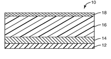
<도 1>
도 1은 본 발명의 예시적인 다층 필름을 도시한 도면.
<도 2>
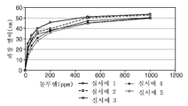
도 2는 유기 분석물 톨루엔의 다양한 노출 수준에서의 예시적인 감지 소자의 측정된 파장 변이의 도면.
<도 3>
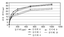
도 3은 유기 분석물 톨루엔의 다양한 노출 수준에서의 예시적인 감지 소자의 측정된 파장 변이의 도면.
<도 4>
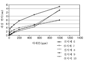
도 4는 유기 분석물 아세톤의 다양한 노출 수준에서의 예시적인 감지 소자의 측정된 파장 변이의 도면.
<도 5>
도 5는 유기 분석물 아세톤의 다양한 노출 수준에서의 예시적인 감지 소자의 측정된 파장 변이의 도면.<Figure 1>
1 illustrates an exemplary multilayer film of the present invention.
<FIG. 2>
FIG. 2 is a plot of measured wavelength variations of exemplary sensing devices at various exposure levels of organic analyte toluene.
3,
FIG. 3 is a diagram of measured wavelength variations of exemplary sensing devices at various exposure levels of organic analyte toluene.
<Figure 4>
4 is a plot of measured wavelength shifts of exemplary sensing elements at various exposure levels of organic analyte acetone.
<Figure 5>
FIG. 5 is a diagram of measured wavelength variations of exemplary sensing elements at various exposure levels of organic analyte acetone.
본 발명은 다층 광학 센서 필름을 제공한다. 센서 필름은 제1 반사층, 및 제1 반사층 위의 검출층을 포함한다. 일부 실시 형태에서, 검출층 위에 제2 반사층이 제공될 수 있다. 검출층은 소수성이고 비결정성이며 실질적으로 미세다공성인 분석물-감응성 유기실리케이트 조성물을 포함한다. 분석물-감응성 유기실리케이트 조성물은 분석물에 노출시 필름에서의 광학적 변화를 제공한다. 다층 구조는 일정 범위의 화학종을 검출할 수 있는 다양한 화학물질을 포함하기 위한 다목적 플랫폼을 제공한다. 필름은 신속하고, 가역적인 (또는, 일부 경우에, 영구적인) 응답을 제공하도록 설계될 수 있다.The present invention provides a multilayer optical sensor film. The sensor film includes a first reflective layer and a detection layer over the first reflective layer. In some embodiments, a second reflective layer can be provided over the detection layer. The detection layer comprises an analyte-sensitive organosilicate composition that is hydrophobic, amorphous, and substantially microporous. The analyte-sensitive organosilicate composition provides an optical change in the film upon exposure to the analyte. The multi-layered structure provides a versatile platform for containing a variety of chemicals capable of detecting a range of chemical species. The film can be designed to provide a fast, reversible (or, in some cases, permanent) response.
다층 광학 센서 필름은 종래의 광학 센서 구조물보다 많은 이점을 갖는다. 예를 들어, 본 발명의 다층 센서 필름에서, 검출층은 소수성이므로 수증기가 광학 특성의 실질적인 변화를 일으키지 않는다. 또한, 필름은 쉽게 가공될 수 있다 반사층 또는 반사층들은 증발 또는 스퍼터 코팅을 통해 침착될 수 있는 한편, 검출층은 직접 코팅(straightforward coating) 기술을 통해 침착될 수 있다.Multilayer optical sensor films have many advantages over conventional optical sensor structures. For example, in the multilayer sensor film of the present invention, the detection layer is hydrophobic so that water vapor does not cause a substantial change in optical properties. In addition, the film can be easily processed. The reflective layer or reflective layers can be deposited via evaporation or sputter coating, while the detection layer can be deposited via a straightforward coating technique.
본 명세서에서 사용되는 바와 같이, 용어 "분석물"은 화학적 또는 생화학적 분석에서 검출되는 특정 성분을 의미하며, 전형적으로 분석물은 유기 화합물 또는 유기 화합물들의 혼합물이다.As used herein, the term “analyte” refers to a specific component that is detected in a chemical or biochemical assay, typically an analyte or a mixture of organic compounds.
본 명세서에서 사용되는 바와 같이, 용어 "치수적 변화"는 검출층의 표면에 수직인 방향에서의 거리의 변화를 말한다.As used herein, the term "dimensional change" refers to a change in distance in a direction perpendicular to the surface of the detection layer.
본 명세서에서 사용되는 바와 같이, 용어 "다공성 재료"는 그의 부피 전반에 기공의 연속적인 네트워크를 포함하는 재료를 의미한다. 미세다공성 재료는 평균 기공 직경이 2 나노미터 이하인 재료이다.As used herein, the term "porous material" means a material that comprises a continuous network of pores throughout its volume. Microporous materials are materials having an average pore diameter of 2 nanometers or less.
본 명세서에서 사용되는 바와 같이, 용어 "반사"는 반반사성이거나 완전히 반사성인 것을 의미한다. 용어 "반반사"는 완전히 반사성도 아니고 완전히 투과성도 아니며, 일반적으로 약 30 내지 약 70% 반사성이거나, 약 40 내지 약 60% 반사성인 것을 의미한다.As used herein, the term "reflective" means either semireflective or completely reflective. The term “reflective” is neither fully reflective nor completely transmissive, and generally means about 30 to about 70% reflective or about 40 to about 60% reflective.
본 명세서에서 사용되는 바와 같이, 용어 "실질적으로 연속적인"은 재료의 층이 비다공성이지만, 재료의 층을 통해 통로를 생성하는 균열, 결정립계(grain boundary), 또는 다른 구조를 가질 수 있음을 의미한다. "실질적으로 연속적인" 층은 비다공성이지만, 하나 이상의 분석물에 대해 침투성일 수 있다.As used herein, the term “substantially continuous” means that the layer of material is nonporous but may have a crack, grain boundary, or other structure that creates a passage through the layer of material. do. A "substantially continuous" layer is nonporous but can be permeable to one or more analytes.
본 명세서에서 사용되는 바와 같이, 용어 "불연속적인"은 사이에 빈 공간을 갖는 적어도 2개의 분리되고 이산된 섬(island)을 가지며, 사이에 빈 공간을 갖는 적어도 2개의 분리되고 이산된 섬은 주어진 평면 내에 있는 재료의 층을 의미한다.As used herein, the term “discontinuous” has at least two separate and discrete islands with empty spaces in between, and at least two separate and discrete islands with empty spaces between Means a layer of material in the plane.
본 명세서에서 사용되는 바와 같이, 용어 "반연속적인"은 다공성이며 액체- 또는 증기-침투성인 재료의 층을 의미한다. 반연속적인 층은 증기-침투성이지만 액체-침투성은 아닐 수 있다.As used herein, the term "semicontinuous" means a layer of material that is porous and liquid- or vapor-permeable. The semicontinuous layer may be vapor-permeable but not liquid-permeable.
본 명세서에서 사용되는 바와 같이, 용어 "증기 침투성"은 일 측면이 검출층과 유체 연통하는 반사층에 대해 사용될 때, 반사층의 타 측면이 20 리터/분으로 유동하는 1000 ppm의 스티렌 단량체 증기를 함유하는 공기 스트림에 15분 동안 노출되는 경우, 검출층 내에서 광학-응답성 변화가 일어나도록 충분한 스티렌 단량체가 반사층을 통과하는 것을 의미한다.As used herein, the term “vapor permeability”, when used for a reflective layer in which one side is in fluid communication with the detection layer, contains 1000 ppm of styrene monomer vapor in which the other side of the reflective layer flows at 20 liters / minute. When exposed to an air stream for 15 minutes, it means that enough styrene monomer passes through the reflective layer to cause an optical-responsive change in the detection layer.
본 명세서에서 사용되는 바와 같이, 용어 "액체-침투성"은 일 측면이 검출층과 유체 연통하는 반사층에 대해 사용될 때, 반사층의 타 측면이 물 중 10 부피%의 아세톤을 포함하는 용액에 10분 동안 노출되는 경우, 검출층 내에서 광학-응답성 변화가 일어나도록 충분한 아세톤이 반사층을 통과하는 것을 의미한다.As used herein, the term "liquid-permeable" when used for a reflective layer in which one side is in fluid communication with the detection layer, the other side of the reflective layer for 10 minutes in a solution comprising 10% by volume of acetone in water. When exposed, it means that enough acetone passes through the reflective layer to cause an optical-responsive change in the detection layer.
본 명세서에서 사용되는 바와 같이, 용어 "미세다공성"은 평균 기공 직경 크기가 약 2 나노미터 미만인 다공성 재료를 지칭한다.As used herein, the term “microporous” refers to a porous material having an average pore diameter size of less than about 2 nanometers.
본 명세서에서 사용되는 바와 같이, 용어 "소수성"은 물을 끌어당기지 않는 조성물을 지칭한다. 조성물의 소수성 특성은 소정 상대 습도에서 소정 기간에 걸친 물의 흡착에 의한 것을 포함하는 다양한 방식으로 측정될 수 있다. 그러한 시험은 실시예 부분에서 더욱 상세하게 정의된다.As used herein, the term "hydrophobic" refers to a composition that does not attract water. Hydrophobic properties of the composition can be measured in a variety of ways, including by adsorption of water over a period of time at a given relative humidity. Such tests are defined in more detail in the Examples section.
본 명세서에서 사용되는 바와 같이, 용어 "비결정성"은 실질적으로 비-결정질인 조성물을 지칭한다. 전형적으로, X-선 회절계로 스캔하는 경우, 조성물은 0.5 내지 80도(2θ)로 스캔할 때 식별가능한 X-선 회절 패턴을 나타내지 않는다.As used herein, the term “amorphous” refers to a composition that is substantially amorphous. Typically, when scanning with an X-ray diffractometer, the composition does not exhibit an identifiable X-ray diffraction pattern when scanning at 0.5 to 80 degrees (2θ).
본 명세서에서 사용되는 바와 같이, 용어 "유기실리케이트"는 공유 결합된 3차원 실리카 네트워크(-Si-O-Si-)와 일부 유기작용기 R을 포함하는 하이브리드인 조성물을 지칭하며, 여기서, R은 적어도 하나의 Si-C 결합에 의해서 실리카 네트워크에 결합된 탄화수소 기 또는 헤테로원자 치환된 탄화수소 기이다.As used herein, the term "organosilicate" refers to a composition that is a hybrid comprising a covalently bonded three-dimensional silica network (-Si-O-Si-) and some organofunctional groups R, wherein R is at least It is a hydrocarbon group or heteroatom substituted hydrocarbon group bonded to a silica network by one Si-C bond.
본 명세서에서 사용되는 바와 같이, 용어 "탄화수소 기"는 탄소와 수소 결합을 포함하는 기를 지칭한다. 탄화수소 기는 선형, 분지형, 환형, 또는 방향족일 수 있다. 탄화수소 기의 예는 알킬 기 및 아릴 기이다.As used herein, the term "hydrocarbon group" refers to a group comprising a carbon and hydrogen bond. Hydrocarbon groups can be linear, branched, cyclic, or aromatic. Examples of hydrocarbon groups are alkyl groups and aryl groups.
본 명세서에서 사용되는 바와 같이, 용어 "치환된 탄화수소 기"는 하나 이상의 헤테로원자, 예를 들어, 산소, 질소, 황, 인, 붕소, 할로겐(F, Cl, Br, 또는 I), 비소, 주석 또는 납을 포함하는 탄화수소 기이다. 헤테로원자는 펜던트형 또는 현수형(catenary)일 수 있다.As used herein, the term "substituted hydrocarbon group" refers to one or more heteroatoms such as oxygen, nitrogen, sulfur, phosphorus, boron, halogen (F, Cl, Br, or I), arsenic, tin Or a hydrocarbon group comprising lead. Heteroatoms may be pendant or catenary.
본 명세서에서 사용되는 바와 같이, 용어 "알킬"은 포화 탄화수소인 알칸의 라디칼인 1가 기를 지칭한다. 알킬은 선형, 분지형, 환형 또는 그 조합일 수 있으며, 전형적으로 1 내지 20개의 탄소 원자를 갖는다. 일부 실시 형태에서, 알킬기는 1 내지 18개, 1 내지 12개, 1 내지 10개, 1 내지 8개, 1 내지 6개 또는 1 내지 4개의 탄소 원자를 포함한다. 알킬기의 예에는 메틸, 에틸, n-프로필, 아이소프로필, n-부틸, 아이소부틸, tert-부틸, n-펜틸, n-헥실, 사이클로헥실, n-헵틸, n-옥틸 및 에틸헥실이 포함되지만, 이들에 한정되는 것은 아니다.As used herein, the term "alkyl" refers to a monovalent group that is a radical of an alkane that is a saturated hydrocarbon. Alkyl may be linear, branched, cyclic, or a combination thereof, and typically has 1 to 20 carbon atoms. In some embodiments, the alkyl group contains 1 to 18, 1 to 12, 1 to 10, 1 to 8, 1 to 6 or 1 to 4 carbon atoms. Examples of alkyl groups include methyl, ethyl, n-propyl, isopropyl, n-butyl, isobutyl, tert-butyl, n-pentyl, n-hexyl, cyclohexyl, n-heptyl, n-octyl and ethylhexyl It is not limited to these.
본 명세서에서 사용되는 바와 같이, 용어 "아릴"은 방향족 및 탄소환식인 1가 기를 지칭한다. 아릴은 방향족환에 연결되거나 융합된 1개 내지 5개의 환을 가질 수 있다. 다른 환 구조는 방향족, 비방향족 또는 이들의 조합일 수 있다. 아릴기의 예로는 페닐, 바이페닐, 터페닐, 안트릴, 나프틸, 아세나프틸, 안트라퀴노닐, 페난트릴, 안트라세닐, 피레닐, 페릴레닐 및 플루오레닐이 포함되지만, 이들에 한정되는 것은 아니다.As used herein, the term "aryl" refers to monovalent groups that are aromatic and carbocyclic. Aryl may have 1 to 5 rings linked or fused to an aromatic ring. Other ring structures can be aromatic, non-aromatic or combinations thereof. Examples of aryl groups include, but are not limited to, phenyl, biphenyl, terphenyl, anthryl, naphthyl, acenaphthyl, anthraquinonyl, phenanthryl, anthracenyl, pyrenyl, perrylenyl and fluorenyl It doesn't happen.
본 명세서에서 사용되는 바와 같이, 용어 "알킬렌"은 알칸의 라디칼인 2가 기를 지칭한다. 알킬렌은 직쇄, 분지형, 환형 또는 이들의 조합일 수 있다. 알킬렌은 종종 1개 내지 20개의 탄소 원자를 갖는다. 일부의 실시형태에서, 알킬렌은 1개 내지 18개, 1개 내지 12개, 1개 내지 10개, 1개 내지 8개, 1개 내지 6개, 또는 1개 내지 4개의 탄소 원자를 포함한다. 알킬렌의 라디칼 중심은 동일한 탄소 원자 상에 (즉, 알킬리덴) 또는 상이한 탄소 원자 상에 존재할 수 있다.As used herein, the term "alkylene" refers to a divalent group that is a radical of an alkane. Alkylene may be straight chain, branched, cyclic, or a combination thereof. Alkylene often has 1 to 20 carbon atoms. In some embodiments, the alkylene comprises 1 to 18, 1 to 12, 1 to 10, 1 to 8, 1 to 6, or 1 to 4 carbon atoms. . The radical centers of the alkylene may be present on the same carbon atom (ie alkylidene) or on different carbon atoms.
본 명세서에서 사용되는 바와 같이, 용어 "아릴렌"은 탄소환식 및 방향족인 2가 기를 지칭한다. 이 기는 연결되거나, 융합되거나, 이들의 조합인 1개 내지 5개의 환을 갖는다. 다른 환은 방향족, 비방향족 또는 이들의 조합일 수 있다. 일부의 실시형태에서, 아릴렌기는 5개 이하의 환, 4개 이하의 환, 3개 이하의 환, 2개 이하의 환 또는 1개의 방향족환을 갖는다. 예를 들어, 아릴렌 기는 페닐렌일 수 있다.As used herein, the term “arylene” refers to a divalent group that is carbocyclic and aromatic. This group has 1 to 5 rings that are linked, fused, or a combination thereof. The other ring may be aromatic, non-aromatic or combinations thereof. In some embodiments, the arylene group has up to 5 rings, up to 4 rings, up to 3 rings, up to 2 rings or 1 aromatic ring. For example, the arylene group can be phenylene.
본 명세서에서 사용되는 바와 같이, 용어 "아르알킬렌"은 화학식 -Ra-Ara-의 2가 기를 지칭하며, 여기서, Ra는 알킬렌이고 Ara는 아릴렌이다(즉, 알킬렌이 아릴렌에 결합된다).As used herein, the term "aralkylene" of the formula -R a -Ar a - refers to a divalent group, wherein, R a is alkylene and Ar a is an arylene (i.e., an alkylene is To arylene).
본 명세서에서 사용되는 바와 같이, 용어 "알콕시"는 화학식 -OR의 기를 지칭하며, 여기서, R은 알킬, 아릴, 또는 치환된 알킬 기이다.As used herein, the term "alkoxy" refers to a group of the formula -OR, where R is an alkyl, aryl, or substituted alkyl group.
본 명세서에서 사용되는 바와 같이, 용어 "아세톡시"는 화학식 -OC(O)CH3의 기를 지칭하며, 여기서, C(O)는 카르보닐 기 C=O를 지칭한다.As used herein, the term “acetoxy” refers to a group of the formula —OC (O) CH 3 , where C (O) refers to a carbonyl group C═O.
본 명세서에서 사용되는 바와 같이, 용어 "아미노"는 화학식 -NR2의 기를 지칭하며, 여기서, R은 알킬, 아릴, 또는 치환된 알킬 기이다.As used herein, the term "amino" refers to a group of the formula -NR 2 , wherein R is an alkyl, aryl, or substituted alkyl group.
본 명세서에서 사용되는 바와 같이, 용어 "기공 크기"는 기공의 직경을 지칭하며 용어 "기공 부피"는 기공의 부피를 지칭한다.As used herein, the term "pore size" refers to the diameter of the pores and the term "pore volume" refers to the volume of the pores.
본 명세서에서 사용되는 바와 같이, 용어 "포로젠"은 다공성 구조체의 형성을 촉진하는 물질을 지칭한다. 용매는 전형적으로 이러한 맥락에서의 포로젠으로 간주되지 않는다.As used herein, the term "porogen" refers to a material that promotes the formation of a porous structure. Solvents are typically not considered porogens in this context.
본 명세서에서 사용되는 바와 같이, 용어 "하소하다" 및 "하소"는 혼합물, 예를 들어, 졸을 용융점 미만의 온도로 가열하여 휘발성 물질을 제거하고 유기실리케이트 네트워크를 형성하는 것을 지칭한다.As used herein, the terms “calcin” and “calcination” refer to heating a mixture, eg, a sol, to a temperature below the melting point to remove volatiles and form organosilicate networks.
본 명세서에서 사용되는 바와 같이, 용어 "졸"은 하소 시에 연속 유기 실리케이트 네트워크를 형성하는, 용매 중에 반응성 유기실리케이트 재료를 포함하는 전구체 혼합물을 지칭한다.As used herein, the term “sol” refers to a precursor mixture comprising a reactive organosilicate material in a solvent that forms a continuous organosilicate network upon calcination.
다층 센서 필름은 제1 반사층, 및 제1 반사층 위의 검출층을 포함한다. 일부 실시 형태에서, 검출층 위에 제2 반사층이 제공된다. 일부 실시 형태에서, 다층 광학 센서 필름은 비색성이며, 광학적 장비가 필요없이 시각적 수단을 사용하여 검출하는 것이 가능하다. 이러한 실시 형태에서, 센서 필름은, 둘 모두 금속 층일 수 있는, 제1 반사층과 선택적인 제2 반사층 사이에 적어도 하나의 분석물-감응성 유기실리케이트 검출층을 포함하는 착색된 필름을 포함할 수 있다. 이러한 다층 필름은 시각적 신호 변환을 위한 일반적인 수단을 제공한다. 필름은 간섭 필터로서 기능하며, 따라서 가시 범위 이내의 특정 파장의 반사로 인해 고도로 착색될 수 있다. 센서 필름의 착색은 적층물 내의 각각의 층의 두께에 따라 크게 좌우된다.The multilayer sensor film includes a first reflective layer and a detection layer over the first reflective layer. In some embodiments, a second reflective layer is provided over the detection layer. In some embodiments, the multilayer optical sensor film is colorimetric and it is possible to detect using visual means without the need for optical equipment. In such embodiments, the sensor film may comprise a colored film comprising at least one analyte-sensitive organosilicate detection layer between the first reflective layer and the optional second reflective layer, which may both be metal layers. Such multilayer films provide a general means for visual signal conversion. The film functions as an interference filter and can therefore be highly colored due to reflection of certain wavelengths within the visible range. Coloring of the sensor film depends heavily on the thickness of each layer in the stack.
본 발명의 다층 센서 필름의 일반적인 도시가 도 1에 나타나있다. 일반적으로, 예시적인 다층 필름 센서(10)는 (선택적인) 기재 층(12), 제1 반사층(14), 검출층(16), 및 (선택적인) 제2 반사층(18)을 포함한다.A general illustration of the multilayer sensor film of the present invention is shown in FIG. In general, the exemplary
센서 필름은 분석물 또는 분석물들의 혼합물의 존재 및/또는 농도를 검출하기 위해 사용될 수 있다. 분석물은 기체(예를 들어 증기) 또는 액체일 수 있다. 분석물은 분자, 거대분자, 생체분자, 또는 생체거대분자일 수 있다. 분석물은 기체 매질(예를 들어, 공기) 또는 액체 매질(예를 들어, 물 또는 기타 유체) 중에 존재할 수 있다. 전형적으로 분석물은 유기 물질이다.Sensor films can be used to detect the presence and / or concentration of analytes or mixtures of analytes. The analyte may be a gas (eg vapor) or liquid. The analyte can be a molecule, macromolecule, biomolecule, or biomacromolecule. The analyte may be present in a gaseous medium (eg air) or in a liquid medium (eg water or other fluid). Typically the analyte is an organic material.
적어도 하나의 실시 형태에서, 분석물은 분석물에 노출될 때의 분석물-감응성 유기실리케이트 검출층의 광학 두께의 변화에 의해서 검출된다. 분석물은 외측 또는 제2 반사층을 통과하며 검출층의 광학 두께를 변화시킨다. 일 실시 형태에서, 분석물은 검출 층의 적어도 일부분 내로 흡착된다. 흡착 시에, (종종 뚜렷한) 색상 변화가 분석물의 존재를 표시할 수 있다.In at least one embodiment, the analyte is detected by a change in the optical thickness of the analyte-sensitive organosilicate detection layer when exposed to the analyte. The analyte passes through the outer or second reflective layer and changes the optical thickness of the detection layer. In one embodiment, the analyte is adsorbed into at least a portion of the detection layer. Upon adsorption, a (often pronounced) color change can indicate the presence of the analyte.
광학 두께의 변화는 전형적으로 가시광 범위 내에서 관찰될 수 있고, 육안에 의해 검출될 수 있다. 그러나, 센서는 UV, 적외선, 또는 근적외선과 같은 다른 광원에 노출될 때 광학 두께의 변화를 나타내도록 설계될 수 있다. 다양한 검출 메커니즘이 사용될 수 있다. 적합한 검출 메커니즘의 예로는 분광 광도계, 광섬유 분광 광도계, 및 광 검출기, 예를 들어 전하 결합 소자(charge coupled device, ccd), 디지털 카메라 등이 포함된다.Changes in optical thickness can typically be observed within the visible range and detected by the naked eye. However, the sensor can be designed to exhibit a change in optical thickness when exposed to other light sources such as UV, infrared, or near infrared. Various detection mechanisms can be used. Examples of suitable detection mechanisms include spectrophotometers, optical fiber spectrophotometers, and photo detectors such as charge coupled devices (ccd), digital cameras, and the like.
다른 실시 형태에서, 분석물은 그 존재가 인접층으로부터의 검출층의 탈층(delamination)을 야기하는 경우에 검출된다. 전형적으로, 탈층은 분석물이 검출층과 인접층의 계면을 적셔서 계면 접착을 감소시킬 때 일어난다. 탈층이 일어날 때, 광학 간섭이 파괴되고 센서는 감지가능한 색상을 잃는다. 인접층과의 계면 면적을 감소시키는 검출층 형상의 변화를 수반하는 이러한 과정은, 센서 필름의 광학 특성을 영구적으로 변화시키는, 재료 내의 결점을 야기한다.In another embodiment, the analyte is detected when its presence causes delamination of the detection layer from adjacent layers. Typically, delamination occurs when the analyte wets the interface of the detection and adjacent layers to reduce the interface adhesion. When delamination occurs, optical interference is broken and the sensor loses a detectable color. This process, accompanied by a change in detection layer shape that reduces the interface area with adjacent layers, results in defects in the material that permanently change the optical properties of the sensor film.
다층 광학 센서는 기재를 포함할 수 있다. 기재는 선택적이지만, 존재하는 경우, 다층 광학 센서에 대한 지지를 제공할 수 있는 임의의 적합한 재료를 포함할 수 있다. 이것은 가요성이거나 비가요성일 수 있다. 기재 재료는 응용에 맞춤될 수 있다. 흔히 기재는 진공 침착 공정에서 사용하기에 적합하다.The multilayer optical sensor may comprise a substrate. The substrate is optional, but, if present, may include any suitable material that can provide support for the multilayer optical sensor. It may be flexible or inflexible. The substrate material can be tailored to the application. Often the substrate is suitable for use in a vacuum deposition process.
제1 반사층은 완전 반사층 또는 반반사 층을 형성할 수 있는 임의의 재료를 포함할 수 있다. 전형적으로, 재료는 두께가 약 5 나노미터 내지 약 1 마이크로미터이다. 일부 실시 형태에서, 두께는 약 20 내지 약 200 nm이다. 더 얇은 층이 전형적으로 제1 반사층을 반반사성으로 만드는 데 사용될 수 있다. 제1 반사층은 전형적으로 제2 반사층보다 더 반사성이 되도록 제조되지만, 분석물의 존재에 대한 응답이 센서 필름의 양측으로부터 나타날 수 있도록 제1 반사층과 제2 반사층의 반사성을 동일하게 만드는 것이 때때로 바람직하다.The first reflective layer may comprise any material capable of forming a fully reflective or semi-reflective layer. Typically, the material is about 5 nanometers to about 1 micrometer in thickness. In some embodiments, the thickness is about 20 to about 200 nm. Thinner layers are typically used to make the first reflective layer semireflective. The first reflecting layer is typically made to be more reflective than the second reflecting layer, but it is sometimes desirable to make the reflectivity of the first reflecting layer and the second reflecting layer the same so that the response to the presence of the analyte can appear from both sides of the sensor film.
제1 반사층에 적합한 재료에는 알루미늄, 크롬, 금, 니켈, 규소, 은, 티타늄, 팔라듐 및 백금과 같은, 금속 또는 반금속이 포함된다. 제1 반사층에 포함될 수 있는 다른 적합한 재료에는 산화크롬 및 산화티타늄과 같은 금속 산화물이 포함된다.Suitable materials for the first reflective layer include metals or semimetals, such as aluminum, chromium, gold, nickel, silicon, silver, titanium, palladium and platinum. Other suitable materials that can be included in the first reflective layer include metal oxides such as chromium oxide and titanium oxide.
일부 예시적인 실시 형태에서, 제1 반사층은 약 90 % 이상의 반사성(즉, 약 10 % 이상의 투과성)이며, 일부 실시 형태에서, 약 99 % 반사성(즉, 약 1 % 투과성)이다. 다른 예시적인 실시 형태에서, 제1 반사층은 반반사층이며, 제1 반사층은 약 20 % 이상의 반사성, 예를 들어, 약 20 내지 약 90 % 반사성, 또는 약 30 내지 약 70 % 반사성이다.In some exemplary embodiments, the first reflective layer is at least about 90% reflective (ie, at least about 10% transmissive), and in some embodiments, is about 99% reflective (ie, at about 1% transmissive). In another exemplary embodiment, the first reflective layer is a semi-reflective layer and the first reflective layer is at least about 20% reflective, eg, about 20 to about 90% reflective, or about 30 to about 70% reflective.
일부 실시 형태에서, 제1 반사층은 또한 기재로서 작용하여, 센서에 대한 지지를 제공한다. 제1 반사층은 실질적으로 연속적인 층 또는 불연속적인 층일 수있다. 또한, 제1 반사층은 하나 이상의 반사층을 포함할 수 있다. 일반적으로, 제1 반사층은 단일 반사층을 포함한다.In some embodiments, the first reflective layer also acts as a substrate, providing support for the sensor. The first reflective layer can be a substantially continuous layer or a discontinuous layer. In addition, the first reflective layer may include one or more reflective layers. In general, the first reflective layer comprises a single reflective layer.
검출층은, 소수성이고 비결정성이며 실질적으로 미세다공성인 분석물-감응성 유기실리케이트 조성물을 포함한다. 대부분의 실시 형태에서, 검출층은 분석물에 노출시 광학 두께가 변화한다. 광학 두께의 변화는 치수 변화, 예를 들어, 팽창 또는 수축으로 인한 층의 물리적 두께의 변화 또는 분석물의 존재 또는 화학 반응으로 인한 검출층의 굴절률의 변화에 의해 야기될 수 있다. 검출층은 하나의 색상으로부터 다른 색상으로, 유색에서 무색으로, 또는 무색에서 유색으로 변화할 수 있다.The detection layer comprises an analyte-sensitive organosilicate composition that is hydrophobic, amorphous, and substantially microporous. In most embodiments, the detection layer changes in optical thickness upon exposure to the analyte. The change in optical thickness may be caused by dimensional changes, for example, a change in the physical thickness of the layer due to expansion or contraction or a change in the refractive index of the detection layer due to the presence or chemical reaction of the analyte. The detection layer can change from one color to another, from color to colorless, or from colorless to colored.
유기실리케이트 조성물은 실리카 프레임워크뿐만 아니라 유기작용기를 포함하는 하이브리드 조성물이다. 유기실리케이트 조성물은 다리형 Si-O-Si 결합을 통해 결합된 RSiO3 단위를 포함하며, 여기서, R은 탄화수소 기 또는 치환된 탄화수소 기일 수 있다. R 기는 공유 Si-C 결합에 의해서 실리카 매트릭스에 결합된다.Organosilicate compositions are hybrid compositions comprising organofunctional groups as well as silica frameworks. The organosilicate composition comprises RSiO 3 units bonded via bridged Si—O—Si bonds, where R may be a hydrocarbon group or a substituted hydrocarbon group. The R group is bonded to the silica matrix by covalent Si-C bonds.
본 발명의 유기실리케이트 조성물은 비교적 높은 유기 함량을 갖는 것으로서 설명될 수 있다. 유기실리케이트 조성물의 비교적 높은 유기 함량은, 하기에 논의된 바와 같이, 유기실리케이트 조성물의 소수성에 영향을 주기 때문에 바람직한 특성이다. 비교적 높은 유기 함량이 다수의 방식으로 달성될 수 있다. 예를 들어, 비교적 작은 탄화수소 기, 예를 들어, 메틸, 에틸, 프로필 등인 R을 갖는 다수의 RSiO3 단위가 존재하여 고도의 유기 함량을 제공할 수 있거나, 또는 비교적 큰 탄화수소 기, 예를 들어, 아릴인 R을 갖는 더 적은 수의 RSiO3 단위가 존재할 수 있다.The organosilicate compositions of the present invention can be described as having a relatively high organic content. The relatively high organic content of the organosilicate composition is a desirable property, as discussed below, because it affects the hydrophobicity of the organosilicate composition. Relatively high organic content can be achieved in a number of ways. For example, a number of RSiO 3 units with R, which are relatively small hydrocarbon groups, such as methyl, ethyl, propyl, etc., may be present to provide a high organic content, or relatively large hydrocarbon groups, for example, There may be fewer RSiO 3 units with R being aryl.
매우 다양한 유기작용기(RSiO3 단위 중의 R 기)가 유기실리케이트 조성물에 사용하기에 적합하다. 유기작용기는 단순한 알킬 또는 알킬렌 기, 예를 들어, 메틸, 에틸, 프로필, 메틸렌, 에틸렌, 프로필렌 등일 수 있거나, 또는 예를 들어 더 복잡한 알킬 기일 수 있다. 유기작용기는 또한 방향족 기 예를 들어, 아릴, 치환된 아릴 등일 수 있다. 일부 실시 형태에서, R 기는 2개의 SiO3 단위에 결합된 알킬렌 또는 아릴렌 기일 수 있다(예를 들어, -O3Si-R-SiO3-). 적합한 아릴 및 아릴렌 기의 예에는, 예를 들어, 페닐, 톨릴, 나프틸, 페닐렌, 톨릴렌, 비스페닐렌 등이 포함된다.A wide variety of organofunctional groups (R groups in RSiO 3 units) are suitable for use in organosilicate compositions. The organofunctional group may be a simple alkyl or alkylene group, for example methyl, ethyl, propyl, methylene, ethylene, propylene, or the like, or may be, for example, a more complex alkyl group. The organofunctional group may also be an aromatic group such as aryl, substituted aryl, and the like. In some embodiments, the R group may be an alkylene or arylene group bonded to two SiO 3 units (eg, —O 3 Si—R—SiO 3 −). Examples of suitable aryl and arylene groups include, for example, phenyl, tolyl, naphthyl, phenylene, tolylene, bisphenylene and the like.
일부 실시 형태에서, 유기실리케이트 조성물은 적어도 일부의 방향족 함량(즉, 아릴 및/또는 아릴렌 기)을 포함할 수 있다. 아릴렌 기가 2개의 규소 원자에 결합되는 경우, 아릴렌 기가 특히 적합한데, 이는 경질의 방향족 환이 바람직한 기공 구조를 제공하는 데 도움이 되는 것으로 여겨지기 때문이다. 특히 적합한 아릴 및 아릴렌 기 중에는 페닐, 나프틸, 및 비스페닐렌이 있다.In some embodiments, the organosilicate composition may comprise at least some aromatic content (ie, aryl and / or arylene groups). When arylene groups are bonded to two silicon atoms, arylene groups are particularly suitable because the hard aromatic rings are believed to help provide the desired pore structure. Among the particularly suitable aryl and arylene groups are phenyl, naphthyl, and bisphenylene.
유기 기는 본래 친유성(oleophilic)(문자 그대로, "기름을 좋아함")이며 물보다는 다른 유기작용성 화학종과 더욱 상용성(compatible)이기 때문에, 유기실리케이트의 유기작용성 특성은 조성물을 소수성으로 만드는 경향이 있다. 조성물의 소수성 특성은 이러한 재료가 대기로부터의 수분을 흡착할 가능성을 줄여준다. 대기로부터의 수분의 흡착은, 특히 이러한 재료가 유기 분자의 감지를 요구하는 센서 응용에 이용되는 경우에 바람직하지 않다. 기공이 환경으로부터 실질적으로 수분을 흡착하는 경우, 기공이 관심 유기 분석물을 흡착하는 능력이 감소될 것이다. 그러나, 본 조성물은 소수성이기 때문에, 환경으로부터의 수분에 의해 비교적 영향을 받지 않는다.Because organic groups are inherently oleophilic (literally “like oil”) and more compatible with other organofunctional species than water, the organofunctional nature of the organosilicates makes the composition hydrophobic. There is a tendency. The hydrophobic nature of the composition reduces the likelihood that these materials will adsorb moisture from the atmosphere. Adsorption of moisture from the atmosphere is undesirable, especially when such materials are used in sensor applications that require the detection of organic molecules. If the pores actually adsorb moisture from the environment, the ability of the pores to adsorb the organic analyte of interest will be reduced. However, because the composition is hydrophobic, it is relatively unaffected by moisture from the environment.
소수성은 다양한 방식으로 측정될 수 있다. 특히 유용한 한 가지 기술은 흡착된 물과 대기 중의 물이 평형을 이루도록 충분한 기간동안 실온에서 소정 상대 습도, 예를 들어, 50% 상대 습도를 갖는 환경에 소수성이고 비결정성이며 실질적으로 미세다공성인 유기실리케이트 조성물을 노출시키는 것이다. 이러한 평형 상태는 시간 대 흡착의 그래프를 그리고 프로파일 곡선이 평탄역을 이루는 곳을 관측하여 결정할 수 있다. 전형적으로 필름은 평형에서 50%의 상대 습도에서, 이용가능한 기공 부피의 75% 미만에 물을 흡착한다. 일부 실시 형태에서, 필름은 평형에서 50%의 상대 습도에서, 이용가능한 기공 부피의 65% 미만 또는 심지어 50% 미만에 물을 흡착한다. 일부 실시 형태에서, 필름은 평형에서 50%의 상대 습도에서, 이용가능한 기공 부피의 30% 미만에 물을 흡착한다.Hydrophobicity can be measured in a variety of ways. One particularly useful technique is an organosilicate which is hydrophobic, amorphous and substantially microporous in an environment having a certain relative humidity, eg, 50% relative humidity, at room temperature for a period sufficient to equilibrate the adsorbed and atmospheric water. To expose the composition. This equilibrium can be determined by plotting time vs. adsorption and observing where the profile curve is flat. Typically the film adsorbs water at less than 75% of the available pore volume at 50% relative humidity at equilibrium. In some embodiments, the film adsorbs water at less than 65% or even less than 50% of the available pore volume at 50% relative humidity at equilibrium. In some embodiments, the film adsorbs water at less than 30% of the available pore volume at 50% relative humidity at equilibrium.
유기실리케이트 조성물은 비결정성이거나 실질적으로 비결정성이며, 이는 결정성이 없거나 본질적으로 없음을 의미한다. 이론에 의해 제한하고자 하지는 않지만, 비결정성 유기실리케이트는 더욱 다양한 다공성 구조를 포함하며 그로 인해, 예를 들어, 감지 응용에서, 광범위한 분석물에 대해 적합하다고 믿어진다.The organosilicate composition is amorphous or substantially amorphous, meaning that it is crystalline or essentially free. Without wishing to be bound by theory, it is believed that amorphous organosilicates include more diverse porous structures and are therefore suitable for a wide range of analytes, for example in sensing applications.
유기실리케이트 조성물의 비결정성 특성은, 예를 들어, X-선 회절계를 사용하여 측정될 수 있다. 전형적으로, X-선 회절계로 스캔하는 경우, 조성물은 0.5 내지 80도(2θ)로 스캔할 때 식별가능한 X-선 회절 패턴을 나타내지 않는다. 식별가능한 X-선 회절 패턴이 없다는 것은 X-선 회절 데이터가 본질적으로 특징이 없음을 의미하며, 이는 구조적 규칙성(structural order)이 존재한다는 증거가 없음을 나타낸다.The amorphous nature of the organosilicate composition can be measured using, for example, an X-ray diffractometer. Typically, when scanning with an X-ray diffractometer, the composition does not exhibit an identifiable X-ray diffraction pattern when scanning at 0.5 to 80 degrees (2θ). The absence of an identifiable X-ray diffraction pattern means that the X-ray diffraction data is inherently uncharacteristic, indicating that there is no evidence that there is a structural order.
유기실리케이트 조성물은 실질적으로 미세다공성이다. 다공성 재료는 많은 상이한 방식으로 분류되어 왔다. 다공성 재료에 대한 IUPAC 정의는 평균 기공 직경이 2 나노미터 미만인 다공성 재료를 미세다공성으로, 평균 기공 직경이 2 내지 50 나노미터인 다공성 재료를 메조다공성으로, 그리고 평균 기공 직경이 50 나노미터 초과인 다공성 재료를 거대다공성(macroporous)으로 정의한다. 본 발명의 유기실리케이트 조성물에서는, 전체 기공 부피의 50% 이상이 2.0 나노미터 이하의 직경을 갖는 기공을 포함한다. 일부 실시 형태에서, 전체 기공 부피의 50% 이상이 0.6 내지 1.3 나노미터의 직경을 갖는 기공을 포함한다.The organosilicate composition is substantially microporous. Porous materials have been classified in many different ways. IUPAC definitions for porous materials include microporous for porous materials with an average pore diameter of less than 2 nanometers, mesoporous for porous materials with an average pore diameter of 2 to 50 nanometers, and porosity with an average pore diameter greater than 50 nanometers. The material is defined as macroporous. In the organosilicate composition of the present invention, at least 50% of the total pore volume comprises pores having a diameter of 2.0 nanometers or less. In some embodiments, at least 50% of the total pore volume comprises pores having a diameter of 0.6-1.3 nanometers.
일부 실시 형태에서, 본 발명의 검출층은 유기실리케이트 필름으로서 설명될 수 있으며, 그러한 유기실리케이트 필름은 포로젠을 전형적으로 포함하지 않는 전구체 혼합물로부터 제조된다. 이러한 맥락에서, 포로젠은 다공성 구조의 형성에 도움을 주기 위해 전구체 혼합물에 첨가되는 화학 화합물을 지칭한다. 상이한 목적을 위해 반응 혼합물에 첨가되는 용매 및 다른 성분은 포로젠으로서 간주되지 않는다. 다른 실시 형태에서, 원한다면 선택적인 포로젠이 첨가될 수 있다.In some embodiments, the detection layer of the present invention may be described as an organosilicate film, which organosilicate film is prepared from a precursor mixture that typically does not contain porogens. In this context, porogen refers to a chemical compound added to the precursor mixture to aid in the formation of the porous structure. Solvents and other components added to the reaction mixture for different purposes are not considered as porogens. In other embodiments, optional porogens may be added if desired.
전형적으로 전구체 혼합물을 제조하고, 기재 상에 코팅하고, 가열하여 전구체 혼합물을 건조 및/또는 하소시켜서, 소수성이고 비결정성이며 실질적으로 미세다공성인 유기실리케이트 필름을 형성한다.Typically the precursor mixture is prepared, coated onto a substrate and heated to dry and / or calcinate the precursor mixture to form an hydrophobic, amorphous, substantially microporous organosilicate film.
전구체 혼합물은 다양한 상이한 재료를 포함할 수 있다. 적합한 재료 중에는 용매, 2개 이상의 가수분해성 실란, 선택적인 포로젠 및 산이 있다. 일부 실시 형태에서, 중합체 화학종이 미세다공성 유기실리케이트 네트워크의 형성을 방해하지 않기만 한다면 전구체 혼합물은 다공성이거나 비다공성일 수 있는 선택적인 중합체 화학종을 포함할 수 있다. 그러한 중합체 화학종의 예에는, 예를 들어, 폴리푸르푸릴 알코올, 다당류, 폴리에테르, 폴리올레핀, 폴리스티렌 등이 포함된다.The precursor mixture may comprise a variety of different materials. Among the suitable materials are solvents, two or more hydrolyzable silanes, optional porogens and acids. In some embodiments, the precursor mixture may include optional polymer species that may be porous or nonporous as long as the polymer species does not interfere with the formation of the microporous organosilicate network. Examples of such polymer species include, for example, polyfurfuryl alcohol, polysaccharides, polyethers, polyolefins, polystyrenes, and the like.
전형적으로 전구체 혼합물은 적어도 하나의 용매를 포함한다. 용매 또는 용매들은 반응물을 용해시키거나 희석시키는 기능을 하며 전구체 혼합물에서 일어나는 가수분해 및 축합 반응을 위한 반응 매질로서 기능한다. 용매는 반응물을 적어도 부분적으로 용해시킬 수 있어야 한다. 흔히 수성 시약, 예를 들어, 수성 산이 사용되기 때문에, 전형적으로 용매는 물과 적어도 부분적으로 혼화성이다. 적합한 용매에는, 예를 들어, 알코올, 예를 들어, 메탄올, 에탄올, 아이소프로판올, tert-부탄올; 케톤, 예를 들어, 아세톤 및 메틸 에틸 케톤; 에테르, 예를 들어, 테트라하이드로푸란; 에스테르, 예를 들어, 에틸 아세테이트; 아미드, 예를 들어, 다이메틸포름아미드; 또는 그 혼합물이 포함된다.Typically the precursor mixture comprises at least one solvent. The solvent or solvents serve to dissolve or dilute the reactants and serve as a reaction medium for the hydrolysis and condensation reactions that occur in the precursor mixture. The solvent should be able to at least partially dissolve the reactants. Typically aqueous solvents are used, such as aqueous acids, so that the solvent is typically at least partially miscible with water. Suitable solvents include, for example, alcohols such as methanol, ethanol, isopropanol, tert-butanol; Ketones such as acetone and methyl ethyl ketone; Ethers such as tetrahydrofuran; Esters such as ethyl acetate; Amides such as dimethylformamide; Or mixtures thereof.
전구체 혼합물은 적어도 하나의 가수분해성 실란을 포함한다. 가수분해성 실란은 일반식 Rn-{Si(Z)4-n}x(여기서, R은 x-원자가 탄화수소 기 또는 치환된 탄화수소 기이고, x는 1 이상의 정수이고, Z는 가수분해성 기이고, n은 1, 2 또는 3의 정수임)의 화합물이다. 적합한 가수분해성 기에는 알콕시, 할로, 아세톡시, 및 아미노 기가 포함된다. 일부 실시 형태에서, x는 1이고, n은 1이고, R 기는 탄화수소 기, 예를 들어, 알킬 또는 아릴 기이고, Z는 알콕시이다. 다른 실시 형태에서, x는 2이고, n은 1이고, R은 알킬렌, 아릴렌, 아르알킬렌 기이고, Z는 알콕시이다.The precursor mixture comprises at least one hydrolyzable silane. The hydrolyzable silane is of the general formula R n- {Si (Z) 4-n } x (where R is an x-membered hydrocarbon group or a substituted hydrocarbon group, x is an integer of at least 1, Z is a hydrolyzable group, n is an integer of 1, 2 or 3). Suitable hydrolyzable groups include alkoxy, halo, acetoxy, and amino groups. In some embodiments, x is 1, n is 1, the R group is a hydrocarbon group, such as an alkyl or aryl group, and Z is alkoxy. In another embodiment, x is 2, n is 1, R is an alkylene, arylene, aralkylene group and Z is alkoxy.
일부 실시 형태에서, 전구체 혼합물은 2개 이상의 가수분해성 실란을 포함한다. 일부 실시 형태에서, 전구체 혼합물은 일반식 R1-Si(OR2)3의 가수분해성 실란뿐만 아니라 일반식(R3O)3Si-R5-Si(OR4)3의 가수분해성 실란을 포함하며, 여기서, R1, R2 , R3, 및 R4 , 는 알킬 또는 아릴 기이고, R5는 알킬렌, 아릴렌, 또는 아르알킬렌 기이다. 적합한 가수분해성 실란의 예에는, 예를 들어, 메틸 트라이메톡시 실란, 에틸 트라이메톡시 실란, 페닐 트라이메톡시 실란, 4,4'-비스(트라이에톡시실릴)-1,1'-바이페닐 등이 포함된다. 일부 실시 형태에서, 전구체 혼합물은 페닐 트라이메톡시 실란과 4,4'-비스(트라이에톡시실릴)-1,1'-바이페닐을 포함한다.In some embodiments, the precursor mixture comprises two or more hydrolyzable silanes. In some embodiments, the precursor mixture comprises hydrolyzable silanes of general formula R 1 -Si (OR 2 ) 3 as well as hydrolyzable silanes of general formula (R 3 O) 3 Si-R 5 -Si (OR 4 ) 3 . Wherein R 1 , R 2 , R 3 , and R 4 , Is an alkyl or aryl group and R 5 is an alkylene, arylene, or aralkylene group. Examples of suitable hydrolyzable silanes include, for example, methyl trimethoxy silane, ethyl trimethoxy silane, phenyl trimethoxy silane, 4,4'-bis (triethoxysilyl) -1,1'-biphenyl Etc. are included. In some embodiments, the precursor mixture comprises phenyl trimethoxy silane and 4,4'-bis (triethoxysilyl) -1,1'-biphenyl.
전구체 혼합물 중에 존재하는 가수분해성 실란의 양은 가수분해성 실란 또는 실란들의 특성 및 형성되는 유기실리케이트 조성물의 원하는 특성에 따라 달라질 것이다. 전형적으로, 가수분해성 실란은 전구체 혼합물의 총 중량을 기준으로 약 5 내지 25 중량%의 범위로 존재한다.The amount of hydrolyzable silane present in the precursor mixture will depend on the nature of the hydrolyzable silane or silanes and the desired properties of the organosilicate composition formed. Typically, the hydrolyzable silane is present in the range of about 5 to 25 weight percent based on the total weight of the precursor mixture.
전구체 혼합물은 가수분해성 실란의 가수분해 및 축합 반응을 촉진하기 위해 산을 포함한다. 전구체 혼합물과 상용성이고 가수분해 반응에 도움이 되기만 한다면 임의의 적합한 산이 사용될 수 있다. 적합한 산의 예에는, 예를 들어, 유기산, 포스포늄산, 암모늄산 및 무기산이 포함된다. 유기산은, 예를 들어, 카르복실산, 예를 들어, 아세트산, 설폰산, 예를 들어, 알킬 설폰산, 포스폰산, 예를 들어, 일반식 RP(O)(OH)2 (여기서, R은 알킬 기임)의 알킬 포스폰산, 및 포스핀산, 예를 들어, 일반식 R2P(O)(OH)(여기서, 각각의 R은 독립적으로 알킬 기임)의 알킬 포스핀산을 포함한다. 포스포늄산은 R3PH+(여기서, 각각의 R은 독립적으로 수소이거나, 알킬, 또는 아릴 기임) 유형의 화합물을 포함한다. 암모늄산은 R3NH+(여기서, 각각의 R은 독립적으로 수소이거나, 알킬, 또는 아릴 기임) 유형의 화합물을 포함한다. 무기산은 예를 들어, 염산, 질산, 황산, 붕산, 인산, 플루오르화수소산 등을 포함하는 무기산이다. 전형적으로 무기산은 수성 형태로 사용되며, 즉, 산이 물에 용해된다. 일반적으로, 이용가능성 및 사용의 용이성으로 인해, 수성 무기산이 사용된다. 일부 실시 형태에서, 산은 수성 염산이다.The precursor mixture includes an acid to promote the hydrolysis and condensation reaction of the hydrolyzable silane. Any suitable acid may be used so long as it is compatible with the precursor mixture and aids in the hydrolysis reaction. Examples of suitable acids include, for example, organic acids, phosphonic acids, ammonium acids and inorganic acids. The organic acid can be, for example, carboxylic acid, for example acetic acid, sulfonic acid, for example alkyl sulfonic acid, phosphonic acid, for example general formula RP (O) (OH) 2 , wherein R is Alkyl phosphonic acids of the alkyl group) and phosphinic acids, for example alkyl phosphinic acids of the general formula R 2 P (O) (OH), wherein each R is independently an alkyl group. Phosphonic acids include compounds of the type R 3 PH + , wherein each R is independently hydrogen, alkyl, or an aryl group. Ammonium acid includes compounds of the type R 3 NH + , wherein each R is independently hydrogen, alkyl, or an aryl group. Inorganic acids are inorganic acids including, for example, hydrochloric acid, nitric acid, sulfuric acid, boric acid, phosphoric acid, hydrofluoric acid and the like. Typically the inorganic acid is used in aqueous form, ie the acid is dissolved in water. In general, aqueous inorganic acids are used because of their availability and ease of use. In some embodiments, the acid is aqueous hydrochloric acid.
전구체 혼합물은 선택적으로 적어도 하나의 포로젠을 포함할 수 있다. 포로젠은 다공성 구조의 형성을 촉진하는 물질이다. 포로젠은 유기실리케이트 조성물에 공유적으로 부착되지 않으며 전형적으로 하소 동안 또는 후에 유기실리케이트 조성물 혼합물로부터 제거된다. 일반적으로 포로젠은 전구체 혼합물 중 반응성 화학종과 반응하는 임의의 작용기를 포함하지 않는다.The precursor mixture may optionally include at least one porogen. Porogens are substances that promote the formation of porous structures. Porogens are not covalently attached to the organosilicate composition and are typically removed from the organosilicate composition mixture during or after calcination. In general, porogens do not include any functional groups that react with reactive species in the precursor mixture.
적합한 포로젠의 예에는 폴리에테르 계면활성제, 알킬 암모늄 염, 탄화수소, 예를 들어, 1,3,5-트라이메틸 벤젠 등이 포함된다. 일부 실시 형태에서, 포로젠은 할라이드 반대이온을 갖는 암모늄 염, 예를 들어, 알킬 암모늄 염이다. 그러한 염의 예에는 테트라메틸암모늄 클로라이드, 테트라에틸암모늄 클로라이드, 테트라프로필암모늄 클로라이드, 테트라-n-부틸암모늄 클로라이드, 옥틸트라이메틸암모늄 브로마이드, 데실트라이메틸암모늄 브로마이드, 세틸트라이메틸암모늄 브로마이드 등이 포함된다. 한 가지 특히 적합한 포로젠은 옥틸트라이메틸암모늄 브로마이드이다. 전형적으로, 포로젠은 전구체 혼합물 중에 1 내지 25 중량% 범위의 양으로 존재한다.Examples of suitable porogens include polyether surfactants, alkyl ammonium salts, hydrocarbons such as 1,3,5-trimethyl benzene and the like. In some embodiments, the porogen is an ammonium salt with a halide counterion, such as an alkyl ammonium salt. Examples of such salts include tetramethylammonium chloride, tetraethylammonium chloride, tetrapropylammonium chloride, tetra-n-butylammonium chloride, octyltrimethylammonium bromide, decyltrimethylammonium bromide, cetyltrimethylammonium bromide and the like. . One particularly suitable porogen is octyltrimethylammonium bromide. Typically, the porogen is present in the precursor mixture in an amount ranging from 1 to 25% by weight.
미세다공성 구조의 형성을 방해하지만 않는다면 다른 선택적인 첨가제가 전구체 혼합물에 첨가될 수 있다. 구체적으로, 특히 수성 산이 사용되지 않는 경우, 물이 전구체 혼합물에 첨가될 수 있다.Other optional additives may be added to the precursor mixture as long as they do not interfere with the formation of the microporous structure. In particular, water may be added to the precursor mixture, especially if no aqueous acid is used.
전구체 혼합물은 기재 상에 침착되어 층을 형성할 수 있다. 기재는 센서 소자의 일부를 형성할 수 있거나, 또는 기재는 전구체가 분석물-감응성 유기실리케이트 재료의 예비형성 필름을 형성하도록 하는 일시적인 기재일 수 있다. 전구체는 예를 들어, 스핀 코팅, 딥 코팅, 롤 코팅, 스프레이 코팅과 같은 다양한 코팅 기술, 및 예를 들어, 잉크젯 인쇄 및 스크린 인쇄를 포함하는 인쇄 기술을 사용하여 기재 상에 침착될 수 있다. 스핀 코팅이 특히 유용하다.The precursor mixture can be deposited on a substrate to form a layer. The substrate may form part of the sensor element, or the substrate may be a temporary substrate that allows the precursor to form a preformed film of analyte-sensitive organosilicate material. Precursors can be deposited on a substrate using various coating techniques, such as, for example, spin coating, dip coating, roll coating, spray coating, and printing techniques including, for example, inkjet printing and screen printing. Spin coating is particularly useful.
기재는, 위에서 유기실리케이트 층을 제조하는 것이 바람직하며 유기실리케이트 층을 형성하기 위한 하소 단계를 견뎌낼 수 있는 임의의 적합한 기재일 수 있다. 기재의 예에는, 예를 들어, 금속 및 금속 산화물 플레이트 및 포일, 유리 플레이트, 세라믹 플레이트 및 용품, 규소 웨이퍼, 하소 단계를 견뎌낼 수 있는 중합체, 예를 들어, 폴리아미드 및 실리콘 등이 포함된다. 일부 실시 형태에서, 기재는 센서의 제1 반사층이다.The substrate may preferably be any suitable substrate capable of withstanding the calcination step to form the organosilicate layer, preferably from above. Examples of substrates include, for example, metal and metal oxide plates and foils, glass plates, ceramic plates and articles, silicon wafers, polymers capable of withstanding calcination steps, such as polyamides and silicon, and the like. In some embodiments, the substrate is the first reflective layer of the sensor.
일단 전구체 혼합물이 기재 상에 코팅되면, 혼합물을 건조 및 하소시키기 위해 전형적으로 열처리를 거친다. 가열 단계는 예를 들어, 30 내지 100℃와 같은 비교적 낮은 온도로 될 수 있다. 일반적으로, 가열 단계는 더 높은 온도를 수반한다. 전형적으로, 코팅된 전구체 혼합물은 약 200℃ 내지 약 500℃ 범위의 온도로 가열된다. 일부 실시 형태에서, 가열 단계는 약 450℃로 된다.Once the precursor mixture is coated onto the substrate, it is typically subjected to heat treatment to dry and calcinate the mixture. The heating step can be at a relatively low temperature, for example 30 to 100 ° C. In general, the heating step involves higher temperatures. Typically, the coated precursor mixture is heated to a temperature in the range of about 200 ° C to about 500 ° C. In some embodiments, the heating step is about 450 ° C.
열처리 후에 추가적인 선택 가공 단계가 수행될 수 있다. 예를 들어, 처리제로 유기실리케이트 필름을 처리하는 것이 바람직할 수 있다. 처리제는 유기실리케이트 필름을 추가로 개질하여 예를 들어 더욱 소수성으로 만들 수 있다. 적합한 처리제의 예는 유기실란 처리제, 예를 들어, 알킬 다이실라잔, 예를 들어, 헥사메틸 다이실라잔이다. 그러한 처리는 층을 헥사메틸 다이실라잔의 증기에 노출시켜 수행될 수 있다.Additional heat treatment steps may be performed after the heat treatment. For example, it may be desirable to treat the organosilicate film with a treatment agent. The treating agent can be further modified to an organosilicate film, for example, to make it more hydrophobic. Examples of suitable treating agents are organosilane treating agents such as alkyl disilazane, such as hexamethyl disilazane. Such treatment can be performed by exposing the layer to the vapor of hexamethyl disilazane.
검출층은 임의의 필요한 총 두께를 가질 수 있다. 바람직하게는, 검출층은 총 두께가 약 50 nm 초과, 예를 들어, 약 100 내지 약 1000 nm의 범위이다. 일 실시 형태에서, 검출층은 검출층 전체에 걸쳐 실질적으로 동일한 층 두께를 갖는다. 예를 들어, 도 1의 검출층(16)을 참조한다. 다른 실시 형태에서, 검출층은 검출층 내의 제1 위치로부터 검출층 내의 하나 이상의 다른 위치까지 변화하는 층두께를 갖는다. 또한, 검출층은 불연속적이거나 패턴화될 수 있다. 검출층 위에 적용되는 제2 반사층은 검출층의 두께 편차 및/또는 패턴에 맞도록 적용될 수 있다.The detection layer can have any necessary total thickness. Preferably, the detection layer has a total thickness greater than about 50 nm, for example between about 100 and about 1000 nm. In one embodiment, the detection layer has substantially the same layer thickness throughout the detection layer. See, for example,
선택적인 제2 반사층은 침투성, 반사성, 또는 반반사성 층을 형성할 수 있으며 검출층과는 상이한 굴절률을 갖는 임의의 재료를 포함할 수 있다. 대부분의 실시 형태에서, 재료는 약 5 nm의 두께에서 반반사성인 것이 바람직한데, 이는 이러한 두께에서 대부분의 분석물이 이러한 층을 통과해 검출층으로 침투할 수 있을 것이기 때문이다. 필요한 두께는 층을 형성하기 위해 사용되는 재료, 검출될 분석물, 및 분석물을 운반할 매질에 따라 좌우될 것이다.The optional second reflective layer can form a permeable, reflective, or semireflective layer and can include any material having a different refractive index than the detection layer. In most embodiments, the material is preferably semi-reflective at a thickness of about 5 nm, since at this thickness most analytes will be able to penetrate through this layer and penetrate into the detection layer. The thickness required will depend on the material used to form the layer, the analyte to be detected, and the medium that will carry the analyte.
적합한 재료에는 알루미늄, 크롬, 금, 니켈, 규소, 은, 티타늄, 팔라듐 및 백금과 같은, 금속 및 반금속이 포함된다. 제2 반사층에 포함될 수 있는 다른 적합한 재료에는 산화알루미늄, 산화티타늄 및 산화크롬과 같은 산화물이 포함된다.Suitable materials include metals and semimetals, such as aluminum, chromium, gold, nickel, silicon, silver, titanium, palladium and platinum. Other suitable materials that may be included in the second reflective layer include oxides such as aluminum oxide, titanium oxide and chromium oxide.
제1 반사층과 마찬가지로, 제2 반사층은 실질적으로 연속적인 층 또는 불연속적인 층일 수 있다. 또한, 제1 반사층과 마찬가지로, 제2 반사층은 하나 이상의 반사층 또는 반반사층을 포함할 수 있다. 일반적으로, 제2 반사층은 실질적으로 연속적이거나 불연속적인 단일 반반사층을 포함한다.Like the first reflective layer, the second reflective layer can be a substantially continuous layer or a discontinuous layer. Also, like the first reflective layer, the second reflective layer may include one or more reflective or semi-reflective layers. In general, the second reflective layer includes a single semi-reflective layer that is substantially continuous or discontinuous.
하나의 예시적인 실시 형태에서, 제2 반사층은 실질적으로 연속적인 층이다. 이러한 실시 형태에서, 제2 반사층의 구성 및 조성은 제2 반사층의 상부 표면을 가로질러 그리고 제2 반사층 전체에 걸쳐 실질적으로 일관될 수 있다. 대안적으로, 제2 반사층의 구성 및/또는 조성은 제2 반사층의 상부 표면을 가로질러 그리고 제2 반사층 전체에 걸쳐 변할 수 있다. 예를 들어, 제2 반사층은 차등 침투성을 가져서, 제2 반사층은 제2 반사층의 상부 표면 상의 제1 위치에서 소정 분석물에 대해 더 높은 분석물 침투성을 가지고 상부 표면 상의 제2 위치에서 동일한 분석물에 대해 더 낮은 분석물 침투성을 가질 수 있다. 제2 반사층의 상부 표면 상의 제1 위치 및 제2 위치는 서로에 대해 랜덤하게 위치될 수 있거나, 상부 표면 상에서 패턴을 형성할 수 있다.In one exemplary embodiment, the second reflective layer is a substantially continuous layer. In such embodiments, the configuration and composition of the second reflective layer can be substantially consistent across the top surface of the second reflective layer and throughout the second reflective layer. Alternatively, the configuration and / or composition of the second reflective layer can vary across the top surface of the second reflective layer and throughout the second reflective layer. For example, the second reflective layer has differential permeability such that the second reflective layer has higher analyte permeability for a given analyte at a first location on the top surface of the second reflective layer and the same analyte at the second location on the top surface. May have lower analyte permeability. The first location and the second location on the top surface of the second reflective layer may be randomly positioned relative to each other or may form a pattern on the top surface.
실질적으로 연속적인 제2 반사층은 또한 내부에 패턴을 가질 수 있고, 제2 반사층의 제1 영역은 제2 반사 층의 제2 영역보다 더 큰 광 반사율을 갖는다. 제2 반사층 상의 제1 영역 및 제2 영역은 제2 반사층의 상부 표면 상에 또는 제2 반사층 내에 패턴을 형성할 수 있다. 패턴화된 제2 반사층은, 아래에 놓인 검출층이 분석물에 노출될 때, 착색된 이미지, 단어, 또는 메시지를 생성하도록 패턴을 포함할 수 있다. 제2 반사층은 분석물에 노출 시에 쉽게 식별 가능한 경고를 사용자에게 제공할 수 있다.The substantially continuous second reflecting layer may also have a pattern therein, the first region of the second reflecting layer having a greater light reflectance than the second region of the second reflecting layer. The first region and the second region on the second reflective layer may form a pattern on the top surface of the second reflective layer or in the second reflective layer. The second patterned reflective layer can include a pattern to produce a colored image, word, or message when the underlying detection layer is exposed to the analyte. The second reflective layer can provide a user with an easily identifiable alert upon exposure to the analyte.
제2 반사층의 침투성을 변경하고/하거나 제2 반사층 상에 그리고 제2 반사층 내에 패턴을 생성하기 위해 꽤 많은 방법이 사용될 수 있다. 적합한 방법은 제2 반사층의 두께 또는 밀도를 변화시키기 위해 제2 반사층의 침착 조건을 공간적으로 제어하는 것을 포함하지만 이로 한정되지 않는다. 예를 들어, 침착된 제2 반사층의 두께가 상부 표면 상의 제1 위치로부터 제2 위치까지 변하도록, 침착원과 기재 사이에 마스크가 위치될 수 있다. 제2 반사층 상의 그리고 제2 반사층 내의 패턴의 생성 및/또는 차등 침투성은 또한 제2 반사층의 미세 구조를 변화시키기 위한 레이저 처리와 같은 국부적인 에너지 입력을 사용한 제2 반사층의 후처리에 의해 생성될 수 있다.Quite a number of methods can be used to alter the permeability of the second reflective layer and / or to create a pattern on and in the second reflective layer. Suitable methods include, but are not limited to, spatially controlling the deposition conditions of the second reflective layer to vary the thickness or density of the second reflective layer. For example, a mask can be positioned between the deposition source and the substrate such that the thickness of the deposited second reflective layer varies from a first position to a second position on the top surface. The generation and / or differential permeability of the pattern on the second reflecting layer and in the second reflecting layer may also be produced by the post-treatment of the second reflecting layer using local energy input, such as laser processing to change the microstructure of the second reflecting layer. have.
전술한 방법들 중 어느 방법도 제2 반사층 상에 하나 이상의 패턴을 생성하기 위해 사용될 수 있다. 소정 패턴 또는 패턴들의 선택은 관심 분석물 또는 분석물들, 사용되는 반반사 재료 또는 재료들, 존재한다면 사용자에게 표시되는 메시지, 또는 이들의 조합을 포함하지만 이로 한정되지 않는 많은 요인들에 의존할 수 있다.Any of the methods described above can be used to create one or more patterns on the second reflective layer. The selection of a given pattern or patterns may depend on many factors, including but not limited to the analyte or analytes of interest, the semireflective material or materials used, the message displayed to the user, if present, or a combination thereof. .
실질적으로 연속적인 제2 반사층을 갖는 예시적인 다층 필름이 도 1에 나타나있다. 한 가지 예시적인 다층 필름 센서에서, 다층 필름 센서는 검출층 위에 실질적으로 연속적인 제2 반사층을 포함하며, 검출층은 검출층 내의 하나 이상의 웰(well)의 존재로 인해 분석물의 잠재적으로 향상된 검출을 위한 증가된 표면적을 갖는다. 바람직하게는, 웰을 포함하는 검출층 위에 위치된 실질적으로 연속적인 제2 반사층은 반반사 재료의 단일층이다.An exemplary multilayer film having a substantially continuous second reflective layer is shown in FIG. 1. In one exemplary multilayer film sensor, the multilayer film sensor includes a substantially continuous second reflective layer over the detection layer, which detects potentially improved detection of the analyte due to the presence of one or more wells in the detection layer. For increased surface area. Preferably, the substantially continuous second reflective layer located over the detection layer comprising the wells is a single layer of semireflective material.
추가의 예시적인 실시 형태에서, 제2 반사층은 불연속적인 층이다. 이러한 실시 형태에서, 제2 반사층의 조성은 제2 반사층을 가로질러 실질적으로 일관될 수 있으나; 구역들은 제2 반사층을 둘 이상의 불연속적인 영역으로 분리한다. 불연속적인 제2 반사층은 노출 구역의 "바다" 내에 반반사 섬의 임의의 패턴을 포함할 수 있다(즉, 검출층이 노출됨). 검출층 상의 반반사 섬의 크기 및 밀도는 필요한 대로 변할 수 있고, 검출층의 상부 표면에 걸쳐서 균일하게 분산되거나 불균일하게 분산될 수 있다. 전형적으로, 반반사 섬은 검출층의 상부 표면 위에 균일하게 분포되고, 약 1.0 마이크로미터 이상, 바람직하게는 약 10.0 내지 약 100 마이크로미터의 적어도 하나의 치수(즉, 길이, 폭, 또는 직경)를 갖지만; 임의의 반반사 섬 크기, 형상, 및 밀도가 사용될 수도 있다. 또한, 노출 구역은 전형적으로 약 1.0 내지 약 100 마이크로미터 범위의 적어도 하나의 치수(즉, 길이, 폭, 또는 직경)를 갖지만; 노출 구역은 임의의 치수를 가질 수 있다.In further exemplary embodiments, the second reflective layer is a discontinuous layer. In this embodiment, the composition of the second reflective layer may be substantially consistent across the second reflective layer; The zones separate the second reflective layer into two or more discrete areas. The discontinuous second reflective layer can include any pattern of semi-reflective islands in the “sea” of the exposure zone (ie, the detection layer is exposed). The size and density of the semi-reflective islands on the detection layer may vary as needed, and may be uniformly or non-uniformly distributed over the top surface of the detection layer. Typically, the semi-reflective islands are uniformly distributed over the top surface of the detection layer and have at least one dimension (ie, length, width, or diameter) of at least about 1.0 micrometer, preferably from about 10.0 to about 100 micrometer. Have; Any semi-reflective island size, shape, and density may be used. In addition, the exposure zone typically has at least one dimension (ie, length, width, or diameter) in the range of about 1.0 to about 100 micrometers; The exposed zone can have any dimension.
검출층에 걸쳐 불연속적인 제2 반사층을 제공하기 위한 하나의 적합한 방법으로는 레이저 애블레이션 방법이 포함된다. 제2 반사층의 부분들을 미국 특허 제6,180,318호 및 제6,396,616호에 기재된 바와 같은 레이저에 노출시켜 부분들을 제거할 수 있다. 불연속적인 제2 반사층을 생성하기위해 사용될 수 있는 다른 예시적인 방법은 광 이미징(photo-imaging) 방법이다.One suitable method for providing a discontinuous second reflective layer across the detection layer includes a laser ablation method. Portions of the second reflective layer may be exposed to a laser as described in US Pat. Nos. 6,180,318 and 6,396,616 to remove the portions. Another exemplary method that can be used to create a discontinuous second reflective layer is a photo-imaging method.
일 실시 형태에서, 불연속적인 제2 반사층은 검출층의 상부 표면에 걸쳐 균일하게 분산된 다수의 반반사 섬을 포함하고, 각각의 반반사 섬은 길이, 폭, 또는 직경이 약 1.0 마이크로미터 이상, 더욱 바람직하게는, 약 10.0 내지 약 100 마이크로미터인 정사각형 또는 원의 형상인 상부 표면 구역을 갖는다. 각각의 반반사 섬은 삼각형, 직사각형, 별 형상, 다이아몬드 형상 등을 포함하지만 이로 한정되지 않는 다양한 형상의 상부 표면 구역과, 약 1.0 마이크로미터 이상, 더욱 바람직하게는 약 10.0 내지 약 100 마이크로미터의 하나 이상의 치수를 가질 수 있음을 이해해야 한다. 아울러, 각각의 반반사 섬은 하나 이상의 분석물에 대해 침투성이거나 불침투성일 수 있음을 이해해야 한다. 반반사 섬이 하나 이상의 분석물에 대해 침투성일 때, 센서는 하나 이상의 분석물이 노출 구역을 통해 직접적으로, 뿐만 아니라 반반사 섬을 통해 간접적으로 검출층과 접촉하도록 허용한다.In one embodiment, the discontinuous second reflective layer comprises a plurality of semi-reflective islands uniformly distributed over the top surface of the detection layer, each semi-reflective island having a length, width, or diameter of at least about 1.0 micrometer, More preferably, it has an upper surface area that is in the shape of a square or circle that is about 10.0 to about 100 micrometers. Each semi-reflective island comprises a variety of top surface regions of various shapes, including but not limited to triangles, rectangles, stars, diamonds, and the like, and one of at least about 1.0 micrometers, more preferably about 10.0 to about 100 micrometers. It should be understood that the above dimensions can be obtained. In addition, it should be understood that each semi-reflective island may be permeable or impermeable to one or more analytes. When the semi-reflective islands are permeable to one or more analytes, the sensor allows the one or more analytes to contact the detection layer directly through the exposure zone as well as indirectly through the semi-reflective islands.
레이저 애블레이션 방법(예를 들어, 미국 특허 제6,180,318호 및 제6,396,616호에 기재됨), 화학 에칭 방법, 또는 다른 방법을 사용하여 제2 반사층의 부분들, 뿐만 아니라 검출층의 부분들을 제거하여, 제2 반사층의 상부 표면으로부터 검출층 내로, 아마도 제1 반사층의 상부 표면(또는 선택적인 기재의 상부 표면)까지 연장하는 웰을 형성할 수 있다. 이러한 실시 형태에서, 생성된 구조는 동일한 검출층 조성물 및 제2 반사층 조성물을 갖는 다층 필름 섬(예를 들어, 약 10 마이크로미터의 폭을 갖는 노출 구역의 격자 내의 100 마이크로미터 변을 갖는 정사각형 섬)의 어레이를 포함한다. 제2 반사층 각각의 섬은 하나 이상의 분석물에 대해 침투성이거나 불침투성일 수 있다. 반반사 섬이 하나 이상의 분석물에 대해 침투성인 경우, 다층 구조는 검출층의 상부로부터 뿐만 아니라, 검출층의 측면으로부터 분석물이 검출층 내로 침투하는 것을 가능하게 한다. 생성되는 구조체 내의 다층 필름 섬의 크기, 형상 및 밀도는 상기에 기재된 반반사 섬과 유사하게 변화될 수 있다. 전형적으로, 각각의 다층 필름 섬은 약 1 마이크로미터 이상, 예를 들어, 약 10.0 내지 약 100 마이크로미터의 하나 이상의 치수를 갖는다.Laser ablation methods (such as described in US Pat. Nos. 6,180,318 and 6,396,616), chemical etching methods, or other methods to remove portions of the second reflective layer, as well as portions of the detection layer, Wells may be formed that extend from the top surface of the second reflective layer into the detection layer, perhaps to the top surface of the first reflective layer (or the top surface of the optional substrate). In such an embodiment, the resulting structure is a multilayer film island having the same detection layer composition and the second reflective layer composition (eg, square islands having 100 micrometer sides in the grating of the exposed area having a width of about 10 micrometers). It includes an array of. The islands of each of the second reflective layers can be permeable or impermeable to one or more analytes. If the semi-reflective islands are permeable to one or more analytes, the multilayer structure allows the analytes to penetrate into the detection layer from the top of the detection layer as well as from the side of the detection layer. The size, shape and density of the multilayer film islands in the resulting structure can vary similar to the semi-reflective islands described above. Typically, each multilayer film island has one or more dimensions of at least about 1 micrometer, for example, from about 10.0 to about 100 micrometers.
상기한 방법에 더하여, 다층 필름 섬은 또한 검출층 재료의 섬을 제1 반사층 상에 침착한 다음 제2 반사층을 각각의 검출층 섬의 상부에 침착하여 형성될 수 있다. 잉크젯 인쇄 및 접촉 인쇄를 포함하지만 이로 한정되지 않는 다양한 인쇄 기술이 검출층을 섬 또는 패턴화된 형태로 제1 반사층 상에 침착하는 데 사용될 수 있다.In addition to the method described above, the multilayer film islands may also be formed by depositing islands of detection layer material on the first reflective layer and then depositing a second reflective layer on top of each detection layer island. Various printing techniques, including but not limited to inkjet printing and contact printing, can be used to deposit the detection layer on the first reflective layer in island or patterned form.
반연속적인 제1 반사층 또는 제2 반사층은 금속성 나노입자를 포함할 수 있다. 나노입자 금속성 층 또는 층들은 반사층 또는 반반사 층일 수 있다. 예를 들어, 금속 나노입자의 희석된 코팅 용액 또는 현탁액을 검출층에 적용하고 용액 또는 현탁액이 건조되도록 하여 반연속적인 액체- 또는 증기-침투성 광 반사층을 형성함으로써 제2 반사층을 형성할 수 있다. 희석 수준은, 예를 들어, 적합하게 액체- 또는 증기-침투성인 금속 나노입자 층을 제공할 코팅 용액 또는 현탁액을 제공하는 수준, 예를 들어, 40 중량% 미만, 30 중량% 미만, 20 중량% 미만, 10 중량% 미만, 5 중량% 미만 또는 4 중량% 미만의 고형분 수준일 수 있다. 입수한 그대로의 시판 금속 나노입자 제품을 추가 용매로 희석하고 희석된 용액 또는 현탁액을 적용 및 건조함으로써, 감지 가능하게 얇은 액체- 또는 증기-침투성 층을 얻을 수 있다. 스와빙(swabbing), 딥 코팅, 롤 코팅, 스핀-코팅, 분무 코팅, 다이 코팅, 잉크젯 코팅, 스크린 인쇄(예를 들어, 회전 스크린 인쇄), 그라비어 인쇄, 플렉소 인쇄 및 당업자에게 친숙할 수 있는 다른 기술들을 포함하는 다양한 코팅 기술이 채용되어 금속 나노입자 용액 또는 현탁액을 도포할 수 있다. 스핀-코팅은 다른 방법을 사용하여 얻어지는 것들보다 더 얇고 더 침투성인 코팅을 제공할 수 있다. 따라서, 낮은 고형분 수준으로 입수가능한 일부 은 나노입자 현탁액(예를 들어, 니폰 페인트(Nippon Paint)로부터의 5 중량% SVW001 은 또는 어드밴스드 나노 프로덕츠(Advanced Nano Products)로부터의 10 중량% 실버제트(SILVERJET) DGP-40LT-25C)은 적절하게 높은 속도 및 온도로 적합한 기재 상에 스핀-코팅하는 경우 추가적인 희석없이 입수된 그대로의 형태로 사용할 수 있다. 소결이 적절한 침투성의 손실을 야기하지 않는 한, 금속 나노입자층은 도포된 후에 (예를 들어, 약 125 내지 약 250℃에서 약 10분 내지 약 1시간 동안 가열하여) 소결될 수 있다. 생성된 반사층은 쉽게 확인 가능한 나노입자를 더 이상 포함하지 않을 수 있으나 제조된 방법을 확인하도록 나노입자 반사층이라고 말할 수 있음이 이해될 것이다.The semicontinuous first or second reflecting layer may comprise metallic nanoparticles. The nanoparticle metallic layer or layers can be a reflective layer or a semireflective layer. For example, a second reflective layer can be formed by applying a diluted coating solution or suspension of metal nanoparticles to the detection layer and allowing the solution or suspension to dry to form a semi-continuous liquid- or vapor-permeable light reflective layer. Dilution levels are, for example, levels that provide a coating solution or suspension that will provide a layer of metal nanoparticles that are suitably liquid- or vapor-permeable, for example, less than 40%, less than 30%, 20% by weight. Solids level of less than 10%, less than 5%, or less than 4% by weight. A commercially thin liquid- or vapor-permeable layer can be obtained by diluting the commercial metal nanoparticle product as it is obtained with additional solvent and applying and drying the diluted solution or suspension. Swabbing, dip coating, roll coating, spin-coating, spray coating, die coating, inkjet coating, screen printing (e.g., rotary screen printing), gravure printing, flexo printing and those familiar to those skilled in the art Various coating techniques, including other techniques, can be employed to apply the metal nanoparticle solution or suspension. Spin-coating can provide a thinner and more permeable coating than those obtained using other methods. Thus, some silver nanoparticle suspensions available at low solids levels (eg, 5 wt% SVW001 silver from Nippon Paint or 10 wt% SILVERJET from Advanced Nano Products) DGP-40LT-25C) can be used in the form as it is obtained without further dilution when spin-coating onto a suitable substrate at an appropriately high rate and temperature. Unless sintering causes a loss of proper permeability, the metal nanoparticle layer can be sintered after being applied (eg, by heating from about 125 to about 250 ° C. for about 10 minutes to about 1 hour). It will be appreciated that the resulting reflective layer may no longer contain easily identifiable nanoparticles but may be referred to as nanoparticle reflective layers to confirm the fabricated method.
추가층(또는 추가층들)이 센서 필름의 광학 특성을 방해하지 않기만 한다면 센서 필름은 임의의 상기한 층들 사이에 추가층을 포함할 수 있다. 추가층에는 타이층(tie layer), 구조층 등이 포함될 수 있다.The sensor film may comprise an additional layer between any of the above mentioned layers as long as the additional layer (or additional layers) does not interfere with the optical properties of the sensor film. The additional layer may include a tie layer, a structure layer, and the like.
센서 필름은 또한 제2 반사층 위에 추가층을 포함할 수 있다. 제2 반사층을 적어도 부분적으로 덮을 수 있는 적합한 추가층은, 투명한 층 또는 라미네이트, 및 제2 반사층의 일부분을 하나 이상의 분석물에 대한 노출로부터 일시적으로 또는 영구적으로 차폐하기 위한 마스킹층을 포함한지만 이로 한정되지 않는다. 추가층은 제2 반사층 상에 직접 적용될 수 있거나 또는 타이층 또는 다른 접착층을 통해 제2 반사층에 일시적으로 또는 영구적으로 접합될 수 있다. 필요하다면, 제2 반사층의 외측 표면을 처리하여 추가층에 대한 접합을 향상시킬 수 있다(예를 들어, 화학적 에칭 또는 프라이밍, 전기 방전 처리 등).The sensor film may also include an additional layer over the second reflective layer. Suitable additional layers that can at least partially cover the second reflective layer include, but are not limited to, transparent layers or laminates, and masking layers for temporarily or permanently shielding portions of the second reflective layer from exposure to one or more analytes. It doesn't work. The additional layer may be applied directly on the second reflective layer or may be temporarily or permanently bonded to the second reflective layer via a tie layer or other adhesive layer. If desired, the outer surface of the second reflective layer can be treated to improve bonding to additional layers (eg, chemical etching or priming, electrical discharge treatment, etc.).
예시적인 일 실시 형태에서, 마스킹층이 제2 반사층 위에 패턴의 형태로 제공된다. 이러한 실시 형태에서, 분석물에 노출 시, 센서는 패턴(즉, 제2 반사층 상의 마스킹층의 역 패턴)의 형태로 신호를 나타낸다. 신호 패턴은 형상, 문자, 단어, 사용자에 대한 특정 메시지, 사용자에 대한 안전 지시, 회사 로고 등 포함지만 이로 한정되지 않는 임의의 원하는 형태를 가질 수 있다.In one exemplary embodiment, a masking layer is provided in the form of a pattern over the second reflective layer. In this embodiment, upon exposure to the analyte, the sensor exhibits the signal in the form of a pattern (ie, an inverse pattern of the masking layer on the second reflective layer). The signal pattern may have any desired form, including but not limited to shapes, letters, words, specific messages to the user, safety instructions to the user, company logos, and the like.
본 발명의 다층 필름은 단독으로 사용될 수 있거나 하나 이상의 분석물의 존재 및/또는 농도를 검출하기 위한 장치의 부품일 수 있다. 일 실시 형태에서, 다층 필름 센서는 하우징에 의해 적어도 부분적으로 둘러싸인다. 하우징은 바람직하게는 제2 반사층 위에 위치된 적어도 하나의 개구를 포함하여 적어도 하나의 개구를 통해 제2 반사층을 관찰할 수 있다. 일부 실시 형태에서, 하우징은 적어도 하나의 개구를 포함하고, 적어도 하나의 개구는 시야각으로 인한 센서의 관찰가능한 색상의 임의의 잠재적인 변화(및 센서 판독에 관한 사용자의 혼란)를 최소화하기 위해 제2 반사층의 상부 표면의 제한된 관찰을 제공한다. 전형적으로, 제한된 관찰은 수직 관찰(즉, 제2 반사층의 외측 표면에 수직인 위치로부터의 관찰)로부터 ± 30˚, 더욱 바람직하게는, ± 15˚ 각도 내에서 제2 반사층의 상부 표면의 관찰을 허용한다.The multilayer film of the present invention may be used alone or may be part of an apparatus for detecting the presence and / or concentration of one or more analytes. In one embodiment, the multilayer film sensor is at least partially surrounded by the housing. The housing preferably includes at least one opening positioned over the second reflective layer so that the second reflective layer can be viewed through the at least one opening. In some embodiments, the housing includes at least one opening, the at least one opening being second to minimize any potential change in the observable color of the sensor due to the viewing angle (and confusion of the user regarding sensor readings). Provides limited viewing of the top surface of the reflective layer. Typically, the limited observation is to observe the top surface of the second reflective layer within ± 30 °, more preferably ± 15 ° from the vertical observation (ie, from a position perpendicular to the outer surface of the second reflective layer). Allow.
하우징(또는 상기한 선택적인 기재)은 또한 필름이 아치형 또는 원통형 형상이 되도록 본 발명의 다층 필름 센서를 구속하는 데 사용될 수 있다. 그러한 형태는 색상의 변이를 최소화하면서 사용자가 더 큰 범위의 관찰 각도로부터 센서를 관찰할 수 있게 한다.The housing (or optional substrate described above) can also be used to constrain the multilayer film sensor of the present invention such that the film is arcuate or cylindrical in shape. Such a form allows the user to observe the sensor from a larger range of viewing angles while minimizing color shifts.
상기에 논의된 바와 같이, 본 발명의 다층 필름 센서는 실질적으로 연속적인 제2 반사층 또는 불연속적인 제2 반사층을 가질 수 있다. 예시적인 일 실시 형태에서, 센서는 실질적으로 연속적인 제1 반사층; 제1 반사층 위의 검출층 - 검출층은, 실질적으로 미세다공성이고 비결정성이며 소수성인 분석물-응답성 유기실리케이트 재료를 포함함 -; 검출층 위의 실질적으로 연속적인 제2 반사층 - 제2 반사층은 검출층의 굴절률과 상이한 굴절률을 가지며 소정 분석물에 대해 침투성임 - 을 포함한다. 바람직하게는, 실질적으로 연속적인 제1 반사층, 실질적으로 연속적인 제2 반사층, 또는 둘 모두는, 하나 이상의 분석물이 층들 중 어느 하나 또는 둘 모두에 침투할 수 있도록, 반사 또는 반반사 재료의 단일층을 포함하여 층들 중 어느 하나 또는 둘 모두의 두께를 최소화한다.As discussed above, the multilayer film sensor of the present invention may have a substantially continuous second reflective layer or a discontinuous second reflective layer. In one exemplary embodiment, the sensor comprises a substantially continuous first reflective layer; A detection layer over the first reflective layer, the detection layer comprising analyte-responsive organosilicate material that is substantially microporous, amorphous, and hydrophobic; And a substantially continuous second reflective layer over the detection layer, the second reflective layer having a refractive index that is different from the refractive index of the detection layer and permeable to the desired analyte. Preferably, the substantially continuous first reflective layer, the substantially continuous second reflective layer, or both, comprise a single piece of reflective or semireflective material such that one or more analytes can penetrate either or both of the layers. Including the layer minimizes the thickness of either or both of the layers.
다른 예시적인 실시 형태에서, 센서는 제1 반사층; 제1 반사층 위의 검출층; 및 검출층 위의 불연속적인 제2 반사층 - 제2 반사층은 검출층의 굴절률과 상이한 굴절률을 가짐 - 을 포함한다. 이러한 예시적인 실시 형태에서, 센서는 바람직하게는 하기 특징들 중 적어도 하나를 갖는다:In another exemplary embodiment, the sensor comprises a first reflective layer; A detection layer over the first reflective layer; And a discontinuous second reflective layer over the detection layer, the second reflective layer having a refractive index different from that of the detection layer. In this exemplary embodiment, the sensor preferably has at least one of the following features:
(a) 불연속적인 제2 반사층이 반반사 섬의 단일층을 포함한다;(a) the discontinuous second reflective layer comprises a single layer of semi-reflective islands;
(b) 불연속적인 제2 반사층이 10 마이크로미터 초과의 적어도 하나의 치수를 갖는 반반사 섬의 단일층, 및 반반사 섬들 사이의 노출 구역 - 노출 구역은 폭이 적어도 1.0 마이크로미터임 - 을 포함한다;(b) a single layer of semi-reflective islands having a discontinuous second reflective layer having at least one dimension greater than 10 micrometers, and an exposure zone between the semi-reflective islands, the exposure zone being at least 1.0 micrometers wide. ;
(c) 검출층이 검출층 내로 깊이를 연장하는 웰을 포함한다.(c) The detection layer comprises a well extending depth into the detection layer.
본 발명의 다층 필름은 미국 특허 제5,877,895호에 기재된 공정과 같은 방법을 통해 생성될 수 있다. 검출층은 또한 스핀코팅, 용액 코팅, 압출 코팅, 또는 본 기술 분야에 공지된 다른 적합한 기술에 의해 제조될 수 있다. 제1 반사층 및 제2 반사층은 증발, 스퍼터링, 화학 증착(CVD), 플라즈마 침착, 또는 화염 침착(flame deposition)과 같은 표준 증기 코팅 기술에 의해 제조될 수 있다. 제1 반사층 및 제2 반사층을 제조하기 위한 다른 방법은 용액으로부터의 도금이다.The multilayer film of the present invention can be produced by the same method as the process described in US Pat. No. 5,877,895. The detection layer can also be prepared by spin coating, solution coating, extrusion coating, or other suitable technique known in the art. The first reflecting layer and the second reflecting layer can be prepared by standard vapor coating techniques such as evaporation, sputtering, chemical vapor deposition (CVD), plasma deposition, or flame deposition. Another method for producing the first reflective layer and the second reflective layer is plating from a solution.
필름 센서는 센서, 광원, 및 선택적으로, 색 변화에 대해 센서를 감시하는 수단을 포함하는 시스템에서 사용될 수 있다. 광원은 자연 또는 인공 광원일 수 있다. 감시는 다양한 방식으로 이루어질 수 있다. 이는 광 검출기로 또는 다른 적합한 수단에 의해 시각적으로 이루어질 수 있다.The film sensor can be used in a system that includes a sensor, a light source, and optionally means for monitoring the sensor for color changes. The light source can be a natural or artificial light source. Surveillance can be done in a variety of ways. This can be done visually with a light detector or by other suitable means.
분석물은 증기 또는 액체 매질 중에 존재할 수 있다. 예를 들어, 분석물은 대기 중에 또는 액체 용매 중에 존재할 수 있다. 각각의 경우에, 많은 실시 형태에서, 분석물의 적어도 일부분이 필름 센서의 제2 반사층을 통해 침투해 검출층과 상호작용한다.The analyte may be present in the vapor or liquid medium. For example, the analyte may be present in the atmosphere or in a liquid solvent. In each case, in many embodiments, at least a portion of the analyte penetrates through the second reflective layer of the film sensor to interact with the detection layer.
둘 이상의 필름 센서가 함께 사용되어 어레이를 형성할 수 있다. 어레이는 임의의 적합한 구성일 수 있다. 예를 들어, 어레이는 둘 이상의 센서들을 나란하게 포함할 수 있거나, 센서들이 기재의 대향 측면들에 부착되거나 대향 측면들 상에서 구성될 수 있다. 주어진 어레이 내의 센서들은 동일한 유형의 것일 수 있거나 상이할 수 있다. 다층 필름 센서의 어레이는, 화학 제제의 존재만을 검출하는 것에 반하여, 전체적인 어레이로부터의 고유한 응답 신호에 기초하여, 분석물의 식별에 유용할 것이다.Two or more film sensors may be used together to form an array. The array can be of any suitable configuration. For example, the array may include two or more sensors side by side, or the sensors may be attached to or configured on opposite sides of the substrate. The sensors in a given array may be of the same type or may be different. Arrays of multilayer film sensors will be useful for identification of analytes based on inherent response signals from the entire array as opposed to detecting only the presence of a chemical agent.
다층 필름 센서의 어레이는 소정 샘플 매질 중의 하나 이상의 분석물의 존재 및/또는 농도를 검출하도록 소정 적층물 내에서 상이한 검출층 기공 크기 분포, 또는 상이한 검출층 두께, 또는 그 조합을 가질 수 있다.The array of multilayer film sensors can have different detection layer pore size distributions, or different detection layer thicknesses, or combinations thereof in a given stack to detect the presence and / or concentration of one or more analytes in a given sample medium.
일부 실시 형태에서, 어레이는 둘 이상의 센서를 포함하며, 어레이(들) 중의 각각의 센서는 (a) 공동의 제1 반사층을 공유하고 (b) 미세다공성이고 비결정성이며 소수성인 분석물-응답성 유기실리케이트 재료를 갖는 검출층, 및 반반사층 조성물을 갖는 제2 반사층을 포함하는 층들의 적층물을 포함하는 다층 필름 섬을 포함한다. 일반적으로, 검출층 조성물이 어레이 중의 각각의 센서에 대해 유사하며 반반사 조성물이 어레이 중의 각각의 센서에 대해 유사하다.In some embodiments, the array comprises two or more sensors, each sensor in the array (s) (a) sharing a first reflective layer of the cavity and (b) microporous, amorphous, and hydrophobic analyte-responsive And a multilayer film island comprising a stack of layers comprising a detection layer having an organosilicate material and a second reflective layer having a semireflective layer composition. In general, the detection layer composition is similar for each sensor in the array and the antireflective composition is similar for each sensor in the array.
본 발명의 필름 센서는 많은 유용한 응용을 갖는다. 센서는 예를 들어, 광범위한 유기 증기를 검출하는 데 사용될 수 있다. 센서는 용액 또는 가스 내의 주어진 분석물의 존재 및/또는 농도를 검출하기 위해 사용될 수 있다. 센서 어레이는 용액 또는 가스 내에서의 하나 이상의 분석물의 존재 및/또는 농도를 검출하기 위해 사용될 수 있다. 한 가지 가능한 응용에서, 다층 필름 센서는 액체 또는 기체 매질과 단일 센서 소자의 상호작용보다는, 액체 또는 기체 매질과 어레이의 상호작용에 기초하여 전반적인 색상 패턴을 사용자에게 제공한다.The film sensor of the present invention has many useful applications. Sensors can be used, for example, to detect a wide range of organic vapors. Sensors can be used to detect the presence and / or concentration of a given analyte in solution or gas. Sensor arrays can be used to detect the presence and / or concentration of one or more analytes in a solution or gas. In one possible application, the multilayer film sensor provides the user with an overall color pattern based on the interaction of the array with the liquid or gas medium rather than the interaction of a single sensor element with the liquid or gas medium.
사용 전에, 다층 필름 센서는 검출될 분석물이 실질적으로 없다. 사용 전의 "미노출" 다층 필름 센서는 제2 반사층을 통해 관찰했을 때 전형적으로 제1 색상을 나타내거나, 또는 무색이다. 검출될 하나 이상의 분석물에 대해 노출 시, "미노출" 다층 필름 센서는 분석물 함유 센서로 변환된다. 분석물 함유 센서는 제1 색상과 상이한 제2 색상을 나타내거나, 제1 색상으로부터 무색 상태로의 색상 변화를 진행하거나, 무색 상태로부터 색상 함유 상태로의 색상 변화를 진행하거나, 또는 일부 다른 검출가능한 광학적 변화, 예를 들어, 광학 분광법에 의해 감시될 때의 스펙트럼 최대치 또는 최소치의 파장의 변화를 진행한다.Prior to use, the multilayer film sensor is substantially free of analytes to be detected. “Unexposed” multilayer film sensors prior to use typically exhibit a first color or are colorless when viewed through a second reflective layer. Upon exposure to one or more analytes to be detected, the “unexposed” multilayer film sensor is converted to an analyte containing sensor. The analyte containing sensor exhibits a second color different from the first color, undergoes a color change from the first color to a colorless state, a color change from the colorless state to a color containing state, or some other detectable An optical change, for example a change in the wavelength of the spectral maximum or minimum when monitored by optical spectroscopy, is advanced.
임의의 상기한 센서 및 센서들의 어레이는 소정 매질 중의 하나 이상의 분석물을 검출하는 데 사용될 수 있다. 분석물을 검출하는 예시적인 한 방법에서, 방법은 분석물의 존재 또는 부재를 검출하며, 방법은 센서(또는 센서들의 어레이)를 제공하는 단계, 광원을 제공하는 단계, 센서(또는 센서들의 어레이)와 분석물을 포함할 수 있는 매질을 접촉시키는 단계, 및 광학 특성의 변화에 대해서 센서(또는 센서들의 어레이)를 감시하는 단계를 포함한다. 상기에 논의된 바와 같이, 매질은 기체 또는 액체일 수 있다. 또한, 하나 이상의 분석물이 제2 반사층, 제1 반사층, 또는 두 층 모두를 통해 침투할 수 있다.Any of the above sensors and arrays of sensors can be used to detect one or more analytes in a given medium. In one exemplary method of detecting an analyte, the method detects the presence or absence of an analyte, the method comprising providing a sensor (or an array of sensors), providing a light source, a sensor (or an array of sensors) and Contacting the medium, which may include the analyte, and monitoring the sensor (or array of sensors) for changes in optical properties. As discussed above, the medium may be a gas or a liquid. In addition, one or more analytes may penetrate through the second reflective layer, the first reflective layer, or both layers.
실시예Example
이들 실시예는 단지 예시 목적만을 위한 것이며, 첨부된 특허청구범위의 범주를 제한하려는 것이 아니다. 달리 지시되지 않는 한, 실시예 및 본 명세서의 나머지 부분에서 모든 부, 백분율, 비 등은 중량을 기준으로 한다. 사용한 용매 및 기타 시약은, 달리 나타내지 않는 한 미국 위스콘신주 밀워키 소재의 시그마-알드리치 케미칼 컴퍼니(Sigma-Aldrich Chemical Company)로부터 획득하였다.These examples are for illustrative purposes only and are not intended to limit the scope of the appended claims. Unless otherwise indicated, all parts, percentages, ratios, etc. in the examples and the rest of the specification are by weight. Solvents and other reagents used were obtained from Sigma-Aldrich Chemical Company, Milwaukee, WI unless otherwise indicated.

시험 방법Test Methods
기공 크기의 측정Measurement of pore size
기공 크기의 측정은 질소 흡착 측정을 사용하여 수행하였다. 시험할 재료를 100 mm 직경 규소 웨이퍼 상에 코팅하였다. 웨이퍼를 스핀 코팅법을 사용하여 반복 코팅하였고 이어서 실시예에 기재된 바와 같이 하소시켰다. 필름을 회수하여 질소 흡착 측정에 사용하였다. 74 포인트 마이크로 기공 분석을 사용하여 제조사의 지시에 따라 작동시킨 상표명 "퀀타크롬 오토소르빅(QUANTACHROME AUTOSORB IC)"(미국 플로리다주 보인튼 비치 소재의 퀀타크롬 인스트루먼츠(Quantachrome Instruments))으로 입수가능한 기체 흡착 분석기를 사용하여 질소 흡착에 의해서 총 기공 부피를 측정하였다.Measurement of pore size was performed using nitrogen adsorption measurements. The material to be tested was coated on a 100 mm diameter silicon wafer. The wafer was repeatedly coated using spin coating and then calcined as described in the Examples. The film was recovered and used for nitrogen adsorption measurement. Gas adsorption available under the trade name "QUANTACHROME AUTOSORB IC" (Quantachrome Instruments, Boynton Beach, FL) operated according to manufacturer's instructions using 74 point micropore analysis. The total pore volume was measured by nitrogen adsorption using an analyzer.
소수성 측정Hydrophobicity measurement
코팅된 센서 피스(sensor piece)를 제어된 습도 시험 시스템에 넣고 광학 분광법으로 감시하였다. 센서를 감시하기 위해 오션 옵틱스(Ocean Optics) 광섬유 탐침, LS-1 광원 및 USB-2000 분광광도계를 사용하였다. 서모스탯 조절된 물의 용기를 통해 공기를 유동시켜, 제어된 백분율의 상대 습도로 공기 스트림을 발생시켰다. 센서를 2.5 리터/분의 유량의 습한 공기에 노출시키고, 400 nm 내지 800 nm 사이에서 반사된 광학 스펙트럼을 관측하였다. 이어서, 스펙트럼 최대치(또는 최소치)의 파장 변화를 증기의 농도의 함수로서 그렸다. 더 큰 파장 변이는 다공성 재료로의 더 많은 양의 수증기 흡착과 상호관련된다.Coated sensor pieces were placed in a controlled humidity test system and monitored by optical spectroscopy. Ocean Optics fiber optic probes, LS-1 light sources, and USB-2000 spectrophotometers were used to monitor the sensors. Air was flowed through a vessel of thermostat conditioned water to generate an air stream at a controlled percentage of relative humidity. The sensor was exposed to humid air at a flow rate of 2.5 liters / minute and the reflected optical spectrum was observed between 400 nm and 800 nm. The wavelength change of the spectral maximum (or minimum) was then plotted as a function of the concentration of the vapor. Larger wavelength variations are correlated with higher amounts of water vapor adsorption into porous materials.
하기 절차를 사용하여 50% 상대 습도에서 기공을 채우는 물의 양을 측정하였다. 평형에서 50% 상대 습도에서 기공 내에 존재하는 물의 양을 기공에 물이 없을 때 그리고 기공이 물로 본질적으로 채워져 있을 때 존재하는 물의 양과 비교하였다. 이러한 비교를 위해서, 상대적으로 낮은 상대 습도(대략 5% 상대 습도)에서는 기공이 본질적으로 비어있으며 85% 상대 습도 환경 하의 평형에서는 기공이 본질적으로 가득 차 있는 것으로 가정하였다. 5%, 50% 및 85% 상대 습도 하에서 광학 피크 위치의 차이를 측정하였다. 5%와 50% 상대 습도에서의 샘플들 사이의 피크 위치의 차이를 Δ50%로 기록하고, 5%와 85% 상대 습도에서의 샘플들 사이의 피크 이동의 차이를 Δ85%로 기록하였다. 이러한 2가지 값의 비, Δ50%/Δ85%는 50% 상대 습도에서 기공에 존재하는 물의 양을 나타내는 값을 제공한다. 이러한 비에 100%를 곱하여 평형에서 50% 상대 습도에서 물로 채워진 기공의 백분율을 제공한다.The following procedure was used to measure the amount of water filling the pores at 50% relative humidity. The amount of water present in the pores at 50% relative humidity at equilibrium was compared to the amount of water present when the pores were free of water and when the pores were essentially filled with water. For this comparison, it is assumed that the pores are essentially empty at relatively low relative humidity (approximately 5% relative humidity) and the pores are essentially full at equilibrium under an 85% relative humidity environment. The difference in optical peak positions under 5%, 50% and 85% relative humidity was measured. The difference in peak position between samples at 5% and 50% relative humidity was recorded as Δ 50% and the difference in peak shift between samples at 5% and 85% relative humidity was recorded as Δ 85% . The ratio of these two values, Δ 50% / Δ 85% , gives a value indicating the amount of water present in the pores at 50% relative humidity. This ratio is multiplied by 100% to give the percentage of pores filled with water at 50% relative humidity at equilibrium.
증기 노출 방법Vapor exposure method
코팅된 센서 피스를 제어된 증기 송달 시험 시스템에 넣고 광학 분광법으로 감시하였다. 센서를 감시하기 위해 오션 옵틱스 광섬유 탐침, LS-1 광원 및 USB-2000 분광광도계를 사용하였다. 400 nm 내지 800 nm 사이에서 반사된 광학 스펙트럼을 관측하였다. 공기 중의 제어된 농도의 증기를 약 2.5 리터/분의 유량으로 코팅된 섹션으로 도입하였고, 스펙트럼 응답을 감시하였다. 이어서, 스펙트럼 최대치(또는 최소치)의 파장의 변화를 증기의 농도의 함수로서 그렸다. 더 큰 파장 변이는 다공성 재료로의 더 많은 양의 증기 흡착과 상호관련된다.The coated sensor pieces were placed in a controlled vapor delivery test system and monitored by optical spectroscopy. Ocean optics fiber probes, LS-1 light sources and USB-2000 spectrophotometers were used to monitor the sensors. The reflected optical spectrum was observed between 400 nm and 800 nm. A controlled concentration of vapor in air was introduced into the coated section at a flow rate of about 2.5 liters / minute and the spectral response was monitored. The change in wavelength of the spectral maximum (or minimum) was then plotted as a function of the concentration of the vapor. Larger wavelength variations correlate with higher amounts of vapor sorption into porous materials.
유기 증기 감지Organic vapor detection
유기 증기 감지 응용을 위한 이러한 재료의 용도를 입증하기 위해서, 재료를 상이한 농도들에 노출시키고 상기한 증기 노출 방법에 의해 감시하였다.To demonstrate the use of this material for organic vapor sensing applications, the material was exposed to different concentrations and monitored by the vapor exposure method described above.
X-선 산란X-ray scattering
X-선 산란에 대해 샘플을 시험하여 샘플의 비결정성 특성을 측정하였다. 필립스(Philips) 수직 회절계, 구리 Kα 방사선, 및 산란된 방사선의 비례 검출기 레지스트리(proportional detector registry)를 사용하여 반사 기하학 데이터(reflection geometry data)를 서베이 스캔(survey scan)의 형태로 수집하였다. 회절계를 가변 입사 빔(beam) 슬릿, 고정 회절 빔 슬릿 및 그래파이트 회절 빔 모노크로메이터(monochromator)에 장착하였다. 서베이 스캔은 0.04도 단계 크기 및 4초 체류 시간(dwell time)을 사용하여 5 내지 80 도(2θ)에서 수행하였다. 45 kV 및 35 mA의 X-선 발생기 설정치를 이용하였다. 허버(Huber) 4-서클 회절계, 구리 Kα 방사선, 및 산란된 방사선의 신틸레이션 검출기 레지스트리를 사용하여 추가적인 반사 기하학 저각 데이터를 수집하였다. 입사 빔을 700 ㎛ 핀홀로 시준하고 니켈 여과하였다. 0.01도 단계 간격 및 60초 체류 시간을 사용하여 0.5 내지 15도(2θ)에서 스캔을 수행하였다. 40 kV 및 20 mA의 X-선 발생기 설정치를 이용하였다.Samples were tested for X-ray scattering to determine the amorphous properties of the samples. Reflection geometry data was collected in the form of a survey scan using a Philips vertical diffractometer, copper Kα radiation, and a proportional detector registry of scattered radiation. The diffractometer was mounted in a variable incident beam slit, a fixed diffraction beam slit and a graphite diffraction beam monochromator. Survey scans were performed at 5 to 80 degrees (2θ) using a 0.04 degree step size and 4 second dwell time. X-ray generator settings of 45 kV and 35 mA were used. Additional reflective geometry low angle data was collected using a Huber 4-circle diffractometer, copper Kα radiation, and a scintillation detector registry of scattered radiation. The incident beam was collimated with 700 μm pinholes and nickel filtered. Scans were performed at 0.5 to 15 degrees (2θ) using 0.01 degree step intervals and 60 second residence time. X-ray generator settings of 40 kV and 20 mA were used.
합성예Synthetic example : 시약 용액의 제조:Preparation of Reagent Solution:
하기 실시예에서 전구체 혼합물을 제조하는 데 사용되는 일련의 시약 용액을 제조하였다.In the examples below, a series of reagent solutions were used to prepare the precursor mixture.
용액 1Solution 1
폴리에틸렌 병에서 OTAB(0.126 그램), 에탄올(2.102 그램), BTSBP(0.492 그램), 및 0.1 몰 HCl(aq)(0.201 그램)을 조합하였다.OTAB (0.126 grams), ethanol (2.102 grams), BTSBP (0.492 grams), and 0.1 mol HCl (aq) (0.201 grams) were combined in a polyethylene bottle.
용액 2
폴리에틸렌 병에서 OTAB(0.127 그램), 에탄올(2.129 그램), BTSBP(0.445 그램), PTMS(0.052 그램), 및 0.1 Molar HCl(aq)(0.199 그램)을 조합하였다.Combined OTAB (0.127 grams), ethanol (2.129 grams), BTSBP (0.445 grams), PTMS (0.052 grams), and 0.1 Molar HCl (aq) (0.199 grams) in a polyethylene bottle.
용액 3Solution 3
폴리에틸렌 병에서 OTAB(0.124 그램), 에탄올(2.106 그램), BTSBP(0.392 그램), PTMS(0.102 그램), 및 0.1 M HCl(aq)(0.205 그램)을 조합하였다.Combined OTAB (0.124 grams), ethanol (2.106 grams), BTSBP (0.392 grams), PTMS (0.102 grams), and 0.1 M HCl (aq) (0.205 grams) in a polyethylene bottle.
용액 4
폴리에틸렌 병에서 OTAB(0.126 그램), 에탄올(2.112 그램), BTSBP(0.352 그램), PTMS(0.154 그램), 및 0.1 M HCl(aq)(0.203 그램)을 조합하였다.Combined OTAB (0.126 grams), ethanol (2.112 grams), BTSBP (0.352 grams), PTMS (0.154 grams), and 0.1 M HCl (aq) (0.203 grams) in a polyethylene bottle.
용액 5
폴리에틸렌 병에서 OTAB(0.127 그램), 에탄올(2.095 그램), BTSBP(0.300 그램), PTMS(0.201 그램), 및 0.1 M HCl(aq)(0.201 그램)을 조합하였다.OTAB (0.127 grams), ethanol (2.095 grams), BTSBP (0.300 grams), PTMS (0.201 grams), and 0.1 M HCl (aq) (0.201 grams) were combined in a polyethylene bottle.
실시예 1 내지 실시예 5:Examples 1-5
실시예 1 내지 실시예 5를 위해, 표 1에 나타낸 용액을 사용하였다. 용액을 2 센티미터 직경 척(chuck)을 갖는 헤드웨이 리서치(Headway Research) EC101 DT-R790 스핀 코팅기를 사용하여 규소 웨이퍼 상에 스핀 코팅하였다. 스피닝 전에 몇 방울의 용액으로 각각의 규소 웨이퍼 섹션이 잠기게 하였다. 1000 rpm에서 60초 동안 스핀-코팅을 수행하였다. 코팅된 섹션을 박스 퍼니스(box furnace) 내에서 공기 중에서 1℃/min의 속도로 450℃의 온도까지 하소시키고, 450℃에서 5분 유지한 후 점진적으로 주위 온도로 냉각시켰다. 상기 시험 방법에 기재된 바와 같이 소수성 시험을 행하였고, 결과를 표 3에 나타낸다. 상기에 기재된 시험 방법을 사용하여 유기 분석물 아세톤 및 톨루엔을 가지고 유기 증기 감지 시험을 행하였다. 데이터는 도 2(톨루엔) 및 도 4(아세톤)에 나타나있다. 상기에 기재된 시험 방법을 사용하여 실시예 4의 샘플에 대해 X-선 산란 분석을 행하였다. 시험 결과는 구조적 규칙성이 존재한다는 증거가 없는 것으로 나타났다. 얻어진 저각 및 광각 데이터 둘 모두가 본질적으로 특징이 없었다.For Examples 1-5, the solutions shown in Table 1 were used. The solution was spin coated onto a silicon wafer using a Headway Research EC101 DT-R790 spin coater with a 2 centimeter diameter chuck. Each silicon wafer section was submerged with a few drops of solution prior to spinning. Spin-coating was performed at 1000 rpm for 60 seconds. The coated section was calcined in air in a box furnace to a temperature of 450 ° C. at a rate of 1 ° C./min, held at 450 ° C. for 5 minutes and then gradually cooled to ambient temperature. The hydrophobicity test was done as described in the test method above, and the results are shown in Table 3. The organic vapor detection test was conducted with organic analytes acetone and toluene using the test method described above. Data is shown in FIG. 2 (toluene) and FIG. 4 (acetone). X-ray scattering analysis was performed on the sample of Example 4 using the test method described above. Test results showed no evidence of structural regularity. Both the low angle and wide angle data obtained were essentially uncharacteristic.
실시예 3에서 사용된 코팅 용액의 샘플을 사용하여 기공 크기를 측정하기 위한 샘플을 제조하였다. 상기 시험 방법에 나타낸 기공 크기 측정 시험을 사용하여 시험을 행하였다. 시험 결과는 총 기공 부피의 75%가 2.0 나노미터 이하의 기공 직경을 갖는 기공을 포함하며, 총 기공 부피의 70%가 1.5 나노미터 이하의 직경을 갖는 기공을 포함하는 것으로 나타났다.Samples for measuring pore size were prepared using a sample of the coating solution used in Example 3. The test was carried out using the pore size measurement test shown in the above test method. The test results showed that 75% of the total pore volume included pores having a pore diameter of 2.0 nanometers or less, and 70% of the total pore volume included pores having a diameter of 1.5 nanometers or less.
[표 1]TABLE 1

실시예Example 6 내지 6 to 실시예Example 10: 10:
실시예 6 내지 실시예 10을 위해, 표 2에 나타낸 용액을 사용하였다. 용액을 2 센티미터 직경 척을 갖는 헤드웨이 리서치 EC101 DT-R790 스핀 코팅기를 사용하여 규소 웨이퍼 상에 스핀 코팅하였다. 스피닝 전에 몇 방울의 용액으로 각각의 규소 웨이퍼 섹션이 잠기게 하였다. 1000 rpm에서 60초 동안 스핀-코팅을 수행하였다. 코팅된 섹션을 박스 퍼니스 내에서 공기 중에서 1℃/min의 속도로 450℃의 온도까지 하소시키고, 450℃에서 5분 유지한 후 점진적으로 주위 온도로 냉각시켰다. 각각의 실시예 코팅을 HMDS에 노출시켜 후처리하였다. 코팅된 규소 웨이퍼를 HMDS(1 내지 2 밀리리터)의 저장소를 갖는 폴리스티렌 페트리 접시에 놓았다. 페트리 접시를 덮고, 섹션이 24시간 동안 HMDS 증기와 반응하게 두었다. 상기 시험 방법에 기재된 바와 같이 소수성 시험을 행하였고, 결과를 표 3에 나타낸다. 상기에 기재된 시험 방법을 사용하여 유기 분석물 아세톤 및 톨루엔을 가지고 유기 증기 감지 시험을 행하였다. 데이터는 도 3(톨루엔) 및 도 5(아세톤)에 나타나있다.For Examples 6-10, the solutions shown in Table 2 were used. The solution was spin coated onto a silicon wafer using a Headway Research EC101 DT-R790 spin coater with a 2 centimeter diameter chuck. Each silicon wafer section was submerged with a few drops of solution prior to spinning. Spin-coating was performed at 1000 rpm for 60 seconds. The coated sections were calcined in air in a box furnace at a rate of 1 ° C./min to a temperature of 450 ° C., held at 450 ° C. for 5 minutes and then gradually cooled to ambient temperature. Each example coating was post-treated by exposure to HMDS. The coated silicon wafers were placed in a polystyrene petri dish with a reservoir of HMDS (1-2 milliliters). The Petri dish was covered and the section was allowed to react with HMDS vapor for 24 hours. The hydrophobicity test was done as described in the test method above, and the results are shown in Table 3. The organic vapor detection test was conducted with organic analytes acetone and toluene using the test method described above. Data is shown in FIG. 3 (toluene) and FIG. 5 (acetone).
[표 2]TABLE 2

[표 3][Table 3]

실시예Example 11 11
유리 플레이트의 25 × 25 mm2 섹션 상에 티타늄의 10 나노미터 두께 층을 증착하여 기재를 제조하였다. 산화규소의 20 나노미터 두께 층을 증착하여 티타늄을 코팅하였다.The substrate was prepared by depositing a 10 nanometer thick layer of titanium onto a 25 × 25 mm 2 section of glass plate. A 20 nanometer thick layer of silicon oxide was deposited to coat titanium.
다음 순서대로 폴리에틸렌 병에서 조합하여 코팅 용액을 제조하였다: OTAB(0.125 그램), 에탄올(2.102 그램) BTSBP(0.398 그램), PTMS(0.103 그램) 및 0.1 M HCl(aq)(0.201 그램).Coating solutions were prepared by combining in polyethylene bottles in the following order: OTAB (0.125 grams), ethanol (2.102 grams) BTSBP (0.398 grams), PTMS (0.103 grams) and 0.1 M HCl (aq) (0.201 grams).
코팅 용액의 샘플을 사용하여 실시예 11을 제조하였다. 121분 후에, 2 센티미터 직경 척을 갖는 헤드웨이 리서치 EC101 DT-R790 스핀 코팅기를 사용하여 코팅 용액을 상기한 기재 상에 스핀-코팅하였다. 스피닝 전에 몇 방울의 용액으로 섹션이 잠기게 하였다. 1000 rpm에서 60초 동안 스핀-코팅을 수행하였다. 코팅된 샘플을 퍼니스 내에서 공기 중에서 450℃의 온도로 하소시켰다.Example 11 was prepared using a sample of the coating solution. After 121 minutes, the coating solution was spin-coated onto the substrate described above using a Headway Research EC101 DT-R790 spin coater with a 2 centimeter diameter chuck. The sections were immersed in a few drops of solution before spinning. Spin-coating was performed at 1000 rpm for 60 seconds. The coated sample was calcined at 450 ° C. in air in the furnace.
1.0 그램 양의 실버제트 TMD GP 40LT-25C 은 나노입자(메탄올 중 43.25%, 한국 소재의 어드밴스드 나노 프로덕츠 코., 엘티디.(Advanced Nano Products Co., Ltd.))를 2 밀리리터 메탄올에 첨가하여, 16.8% 고형물을 함유하는 희석된 현탁액을 제공하였다. 희석된 현탁액을 하소된 샘플의 유기실리케이트 층 상에 600 rpm으로 스핀 코팅하였다. 샘플을 150℃에서 1시간 동안 공기 중에서 가열하여 은 입자를 부분적으로 소결시켰다.1.0 gram of silverjet TMD GP 40LT-25C silver nanoparticles (43.25% in methanol, Advanced Nano Products Co., Ltd., Korea) was added to 2 milliliters methanol , A diluted suspension containing 16.8% solids was provided. The diluted suspension was spin coated at 600 rpm on the organosilicate layer of the calcined sample. The sample was heated in air at 150 ° C. for 1 hour to partially sinter the silver particles.
Claims (29)
제1 반사층 위의 검출층 - 검출층은 실질적으로 미세다공성이고 비결정성이며 소수성인 분석물-응답성(analyte-responsive) 유기실리케이트 재료를 포함하고, 실질적으로 미세다공성이고 비결정성이며 소수성인 분석물-응답성 유기실리케이트 재료는 기공 부피를 한정하는 미세기공을 포함함 - 을 포함하는 센서.A substantially continuous first reflective layer; And
Detection layer over the first reflective layer—the detection layer comprises analyte-responsive organosilicate material that is substantially microporous, amorphous, and hydrophobic, and is substantially microporous, amorphous, and hydrophobic The responsive organosilicate material comprises micropores defining a pore volume.
검출층 위에 제2 반사층을 추가로 포함하며, 제2 반사층은 검출층의 굴절률과 상이한 굴절률을 갖고, 제2 반사층의 적어도 일부분은 분석물에 대해 침투성인 센서.The method of claim 1,
And a second reflective layer over the detection layer, the second reflective layer having a refractive index different from the refractive index of the detection layer, wherein at least a portion of the second reflective layer is permeable to the analyte.
실질적으로 연속적인 제1 반사층; 및
제1 반사층 위의 검출층 - 검출층은 실질적으로 미세다공성이고 비결정성이며 소수성인 분석물-응답성 유기실리케이트 재료를 포함하고, 실질적으로 미세다공성이고 비결정성이며 소수성인 분석물-응답성 유기실리케이트 재료는 기공 부피를 한정하는 미세기공을 포함함 - 을 포함하는 어레이.At least two sensors, wherein the sensors
A substantially continuous first reflective layer; And
Detection layer over the first reflective layer—the detection layer comprises analyte-responsive organosilicate material that is substantially microporous, amorphous, and hydrophobic, and is substantially microporous, amorphous, and hydrophobic analyte-responsive organosilicate And the material comprises micropores defining a pore volume.
검출층 위에 제2 반사층을 추가로 포함하며, 제2 반사층은 검출층의 굴절률과 상이한 굴절률을 갖고, 제2 반사층의 적어도 일부분은 분석물에 대해 침투성인 어레이.The method of claim 18, wherein the sensor is
And a second reflective layer over the detection layer, the second reflective layer having a refractive index that is different from the refractive index of the detection layer, at least a portion of the second reflective layer being permeable to the analyte.
제1 반사층 위의 검출층 - 검출층은 실질적으로 미세다공성이고 비결정성이며 소수성인 분석물-응답성 유기실리케이트 재료를 포함하고, 실질적으로 미세다공성이고 비결정성이며 소수성인 분석물-응답성 유기실리케이트 재료는 기공 부피를 한정하는 미세기공을 포함함 - ; 및
광원을 포함하는 장치.A substantially continuous first reflective layer;
Detection layer over the first reflective layer—the detection layer comprises analyte-responsive organosilicate material that is substantially microporous, amorphous, and hydrophobic, and is substantially microporous, amorphous, and hydrophobic analyte-responsive organosilicate The material comprises micropores defining a pore volume; And
A device comprising a light source.
검출층 위에 제2 반사층을 추가로 포함하며, 제2 반사층은 검출층의 굴절률과 상이한 굴절률을 갖고, 제2 반사층의 적어도 일부분은 분석물에 대해 침투성인 장치.The method of claim 22,
Further comprising a second reflective layer over the detection layer, the second reflective layer having a refractive index that is different from the refractive index of the detection layer, wherein at least a portion of the second reflective layer is permeable to the analyte.
제1 반사층 위의 검출층 - 검출층은 실질적으로 미세다공성이고 비결정성이며 소수성인 분석물-응답성 유기실리케이트 재료를 포함하고, 실질적으로 미세다공성이고 비결정성이며 소수성인 분석물-응답성 유기실리케이트 재료는 기공 부피를 한정하는 미세기공을 포함함 - 을 포함하는 센서를 제공하는 단계;
광원을 제공하는 단계;
분석물을 포함할 수 있는 매질을 센서와 접촉시키는 단계; 및
광학 특성의 변화에 대해 센서를 감시하는 단계를 포함하는, 분석물의 존재 또는 부재를 검출하는 방법.A substantially continuous first reflective layer, and
Detection layer over the first reflective layer—the detection layer comprises analyte-responsive organosilicate material that is substantially microporous, amorphous, and hydrophobic, and is substantially microporous, amorphous, and hydrophobic analyte-responsive organosilicate The material comprises micropores defining a pore volume;
Providing a light source;
Contacting the medium, which may include the analyte, with the sensor; And
Monitoring the sensor for changes in optical properties.
검출층 위에 제2 반사층을 추가로 포함하며, 제2 반사층은 검출층의 굴절률과 상이한 굴절률을 갖고, 제2 반사층의 적어도 일부분은 분석물에 대해 침투성인 방법.The method of claim 25, wherein the sensor is
Further comprising a second reflective layer over the detection layer, the second reflective layer having a refractive index that is different from the refractive index of the detection layer, wherein at least a portion of the second reflective layer is permeable to the analyte.
Applications Claiming Priority (2)
| Application Number | Priority Date | Filing Date | Title |
|---|---|---|---|
| US14018008P | 2008-12-23 | 2008-12-23 | |
| US61/140,180 | 2008-12-23 |
Related Child Applications (1)
| Application Number | Title | Priority Date | Filing Date |
|---|---|---|---|
| KR1020177001278A Division KR101821936B1 (en) | 2008-12-23 | 2009-12-14 | Organic Chemical Sensor With Microporous organosilicate material |
Publications (1)
| Publication Number | Publication Date |
|---|---|
| KR20110106407A true KR20110106407A (en) | 2011-09-28 |
Family
ID=42288366
Family Applications (2)
| Application Number | Title | Priority Date | Filing Date |
|---|---|---|---|
| KR1020117017170A KR20110106407A (en) | 2008-12-23 | 2009-12-14 | Organic chemical sensor with microporous organosilicate material |
| KR1020177001278A KR101821936B1 (en) | 2008-12-23 | 2009-12-14 | Organic Chemical Sensor With Microporous organosilicate material |
Family Applications After (1)
| Application Number | Title | Priority Date | Filing Date |
|---|---|---|---|
| KR1020177001278A KR101821936B1 (en) | 2008-12-23 | 2009-12-14 | Organic Chemical Sensor With Microporous organosilicate material |
Country Status (7)
| Country | Link |
|---|---|
| US (1) | US8647884B2 (en) |
| EP (1) | EP2376907A4 (en) |
| JP (1) | JP2012513601A (en) |
| KR (2) | KR20110106407A (en) |
| CN (1) | CN102308208B (en) |
| BR (1) | BRPI0918209A2 (en) |
| WO (1) | WO2010075014A2 (en) |
Families Citing this family (10)
| Publication number | Priority date | Publication date | Assignee | Title |
|---|---|---|---|---|
| JP5662945B2 (en) | 2008-12-23 | 2015-02-04 | スリーエム イノベイティブ プロパティズ カンパニー | Organic chemical sensor with microporous organosilicate material |
| US20110257281A1 (en) * | 2008-12-23 | 2011-10-20 | John Christopher Thomas | Amorphous microporous organosilicate compositions |
| RU2490616C2 (en) | 2009-05-22 | 2013-08-20 | 3М Инновейтив Пропертиз Компани | Multilayer colour sensors |
| KR101777078B1 (en) | 2009-05-22 | 2017-09-08 | 쓰리엠 이노베이티브 프로퍼티즈 컴파니 | Multilayer colorimetric sensor arrays |
| US8955515B2 (en) * | 2009-10-23 | 2015-02-17 | 3M Innovative Properties Company | Patterned chemical sensor having inert occluding layer |
| US9442073B2 (en) | 2011-03-28 | 2016-09-13 | 3M Innovative Properties Company | Sensor comprising a masking layer adhesive |
| FR3066603B1 (en) * | 2017-05-22 | 2019-07-05 | Universite D'aix-Marseille | OPTICAL DEVICE FOR DETECTING AND QUANTIFYING VOLATILE COMPOUNDS |
| DK3775845T3 (en) * | 2018-04-12 | 2023-11-27 | Radiometer Medical Aps | SENSOR ELEMENT WITH POROUS MEMBRANE |
| TWI712785B (en) * | 2019-11-15 | 2020-12-11 | 台灣奈米碳素股份有限公司 | Chemical sensor |
| CN116057381A (en) * | 2020-09-15 | 2023-05-02 | 3M创新有限公司 | Nanopatterned films with patterned surface chemistry |
Family Cites Families (51)
| Publication number | Priority date | Publication date | Assignee | Title |
|---|---|---|---|---|
| EP0426989B1 (en) | 1989-11-04 | 1994-02-02 | Dornier Gmbh | Selective gas sensor |
| US5304363A (en) | 1990-01-25 | 1994-04-19 | Mobil Oil Corp. | Porous materials |
| EP0554825B1 (en) * | 1992-02-04 | 1998-10-28 | Matsushita Electric Industrial Co., Ltd. | Direct contact type image sensor and its production method |
| AU6770394A (en) | 1993-05-25 | 1994-12-20 | Rosemount Inc. | Organic chemical sensor |
| US5857250A (en) | 1994-10-25 | 1999-01-12 | Texas Instruments Incorporated | Method of forming a capacitance type gaseous sensing device and apparatus thereof |
| US5877895A (en) | 1995-03-20 | 1999-03-02 | Catalina Coatings, Inc. | Multicolor interference coating |
| TW318320B (en) | 1995-08-07 | 1997-10-21 | Eltech Systems Corp | |
| US5922299A (en) | 1996-11-26 | 1999-07-13 | Battelle Memorial Institute | Mesoporous-silica films, fibers, and powders by evaporation |
| US5892140A (en) | 1997-04-30 | 1999-04-06 | Honeywell Inc. | Micromachined inferential opto-thermal gas sensor |
| US5858457A (en) | 1997-09-25 | 1999-01-12 | Sandia Corporation | Process to form mesostructured films |
| US6696258B1 (en) | 1998-01-20 | 2004-02-24 | Drexel University | Mesoporous materials and methods of making the same |
| US6326326B1 (en) | 1998-02-06 | 2001-12-04 | Battelle Memorial Institute | Surface functionalized mesoporous material and method of making same |
| DE19808936A1 (en) | 1998-03-03 | 1999-09-16 | Aventis Res & Tech Gmbh & Co | Photodetector and its use |
| JP3899733B2 (en) | 1998-07-03 | 2007-03-28 | 株式会社豊田中央研究所 | Porous material and method for producing porous material |
| US6329017B1 (en) | 1998-12-23 | 2001-12-11 | Battelle Memorial Institute | Mesoporous silica film from a solution containing a surfactant and methods of making same |
| US6180318B1 (en) | 1999-05-19 | 2001-01-30 | 3M Innovative Properties Company | Method of imaging an article |
| US6365266B1 (en) | 1999-12-07 | 2002-04-02 | Air Products And Chemicals, Inc. | Mesoporous films having reduced dielectric constants |
| US6592980B1 (en) | 1999-12-07 | 2003-07-15 | Air Products And Chemicals, Inc. | Mesoporous films having reduced dielectric constants |
| US6329062B1 (en) | 2000-02-29 | 2001-12-11 | Novellus Systems, Inc. | Dielectric layer including silicalite crystals and binder and method for producing same for microelectronic circuits |
| US6387453B1 (en) | 2000-03-02 | 2002-05-14 | Sandia Corporation | Method for making surfactant-templated thin films |
| US6270846B1 (en) | 2000-03-02 | 2001-08-07 | Sandia Corporation | Method for making surfactant-templated, high-porosity thin films |
| KR100373210B1 (en) | 2000-04-28 | 2003-02-25 | 주식회사 엘지화학 | Method for preparing dielectrics material with low dielectric constant using organic spacer |
| US6848295B2 (en) | 2002-04-17 | 2005-02-01 | Wayne State University | Acoustic wave sensor apparatus, method and system using wide bandgap materials |
| JP2004504716A (en) | 2000-07-13 | 2004-02-12 | ザ リージェンツ オブ ザ ユニバーシティ オブ カリフォルニア | Silica zeolite low dielectric constant thin film |
| US6396616B1 (en) | 2000-10-10 | 2002-05-28 | 3M Innovative Properties Company | Direct laser imaging system |
| US7141859B2 (en) | 2001-03-29 | 2006-11-28 | Georgia Tech Research Corporation | Porous gas sensors and method of preparation thereof |
| US6713643B2 (en) | 2001-05-24 | 2004-03-30 | Board Of Trustees Of Michigan State University | Ultrastable organofunctional microporous to mesoporous silica compositions |
| JP2005503312A (en) | 2001-09-14 | 2005-02-03 | バッテル メモリアル インスティテュート | Method for producing high purity, low dielectric constant ceramic and hybrid ceramic thin films |
| KR100508903B1 (en) | 2002-05-06 | 2005-08-17 | 주식회사 엘지화학 | Composition for low dielectric film and method for forming low dielectric film |
| US7307343B2 (en) | 2002-05-30 | 2007-12-11 | Air Products And Chemicals, Inc. | Low dielectric materials and methods for making same |
| US20060063178A1 (en) | 2002-06-27 | 2006-03-23 | Trex Enterprises Corporation | Optical sensor and methods for measuring molecular binding interactions |
| JP3704685B2 (en) | 2002-07-29 | 2005-10-12 | 株式会社山武 | Capacitance sensor |
| US7449146B2 (en) * | 2002-09-30 | 2008-11-11 | 3M Innovative Properties Company | Colorimetric sensor |
| US20040062682A1 (en) * | 2002-09-30 | 2004-04-01 | Rakow Neal Anthony | Colorimetric sensor |
| JP4225765B2 (en) | 2002-10-31 | 2009-02-18 | 日揮触媒化成株式会社 | Method for forming low dielectric constant amorphous silica coating and low dielectric constant amorphous silica coating obtained by the method |
| JP4471564B2 (en) * | 2002-10-31 | 2010-06-02 | 日揮触媒化成株式会社 | Coating liquid for forming low dielectric constant amorphous silica film and method for preparing the coating liquid |
| JP4447283B2 (en) | 2003-11-05 | 2010-04-07 | 東京応化工業株式会社 | Coating liquid for silica-based film formation |
| GB2408209A (en) | 2003-11-18 | 2005-05-25 | Qinetiq Ltd | Flexible medical light source |
| US7109130B2 (en) | 2004-05-04 | 2006-09-19 | California Institute Of Technology | Zeolite films for low k applications |
| KR20060020830A (en) | 2004-09-01 | 2006-03-07 | 삼성코닝 주식회사 | Method for preparing surfactant-templated, mesostructured thin film with low dielectric constant |
| KR20060057778A (en) | 2004-11-24 | 2006-05-29 | 삼성코닝 주식회사 | Method for preparing mesoporous thin film with low dielectric constant |
| KR101202955B1 (en) | 2004-12-31 | 2012-11-19 | 삼성코닝정밀소재 주식회사 | Composition for forming low dielectric film comprising porous nanoparticles and method for preparing low dielectric thin film using the same |
| KR101119141B1 (en) | 2005-01-20 | 2012-03-19 | 삼성코닝정밀소재 주식회사 | Composition for forming low dielectric film comprising polymeric nanoparticles and method for preparing low dielectric thin film using the same |
| EP1960487A1 (en) | 2005-12-08 | 2008-08-27 | Queen's University At Kingston | Optical sensor using functionalized composite materials |
| US8293340B2 (en) * | 2005-12-21 | 2012-10-23 | 3M Innovative Properties Company | Plasma deposited microporous analyte detection layer |
| US7556774B2 (en) * | 2005-12-21 | 2009-07-07 | 3M Innovative Properties Company | Optochemical sensor and method of making the same |
| KR100856481B1 (en) | 2006-03-31 | 2008-09-04 | 손홍래 | Chemical sensor sensitive to nitroaromatic compounds using photoluminescent porous silicon |
| US20080006375A1 (en) | 2006-07-06 | 2008-01-10 | Meadows Ralph C | Ornamental screen system |
| US7906223B2 (en) * | 2006-09-11 | 2011-03-15 | 3M Innovative Properties Company | Permeable nanoparticle reflector |
| JP5662945B2 (en) | 2008-12-23 | 2015-02-04 | スリーエム イノベイティブ プロパティズ カンパニー | Organic chemical sensor with microporous organosilicate material |
| US20110257281A1 (en) | 2008-12-23 | 2011-10-20 | John Christopher Thomas | Amorphous microporous organosilicate compositions |
-
2009
- 2009-12-14 BR BRPI0918209-8A patent/BRPI0918209A2/en not_active IP Right Cessation
- 2009-12-14 CN CN200980156137.3A patent/CN102308208B/en not_active Expired - Fee Related
- 2009-12-14 JP JP2011543563A patent/JP2012513601A/en active Pending
- 2009-12-14 KR KR1020117017170A patent/KR20110106407A/en active Application Filing
- 2009-12-14 EP EP09835543.1A patent/EP2376907A4/en not_active Withdrawn
- 2009-12-14 US US13/141,555 patent/US8647884B2/en not_active Expired - Fee Related
- 2009-12-14 WO PCT/US2009/067804 patent/WO2010075014A2/en active Application Filing
- 2009-12-14 KR KR1020177001278A patent/KR101821936B1/en active IP Right Grant
Also Published As
| Publication number | Publication date |
|---|---|
| BRPI0918209A2 (en) | 2021-08-31 |
| WO2010075014A2 (en) | 2010-07-01 |
| US8647884B2 (en) | 2014-02-11 |
| EP2376907A4 (en) | 2017-12-13 |
| US20110257038A1 (en) | 2011-10-20 |
| WO2010075014A3 (en) | 2010-10-28 |
| CN102308208B (en) | 2014-12-03 |
| EP2376907A2 (en) | 2011-10-19 |
| JP2012513601A (en) | 2012-06-14 |
| CN102308208A (en) | 2012-01-04 |
| KR20170010083A (en) | 2017-01-25 |
| KR101821936B1 (en) | 2018-01-24 |
Similar Documents
| Publication | Publication Date | Title |
|---|---|---|
| KR101821936B1 (en) | Organic Chemical Sensor With Microporous organosilicate material | |
| Lova et al. | Label-free vapor selectivity in poly (p-phenylene oxide) photonic crystal sensors | |
| Tran-Thi et al. | Optical chemical sensors based on hybrid organic–inorganic sol–gel nanoreactors | |
| Chocarro-Ruiz et al. | A CO 2 optical sensor based on self-assembled metal–organic framework nanoparticles | |
| RU2490616C2 (en) | Multilayer colour sensors | |
| CN101341404B (en) | Plasma deposited microporous analyte detection layer | |
| US7776611B2 (en) | Optical sensor using functionalized composite materials | |
| Barczak et al. | Micro-and nanostructured sol-gel-based materials for optical chemical sensing (2005–2015) | |
| US20120184047A1 (en) | Nanoplasmonic device | |
| US10656091B2 (en) | Optical sensor for detecting a chemical species | |
| Mironenko et al. | pH-indicators doped polysaccharide LbL coatings for hazardous gases optical sensing | |
| Chauhan et al. | Phenol red dye functionalized nanostructured silica films as optical filters and pH sensors | |
| KR101679441B1 (en) | Amorphous microporous organosilicate compositions | |
| US20160178600A1 (en) | Test strips for visual differentiation of liquid mixture composition | |
| Jung | Fabrication and characterization of DBR porous silicon chip for the detection of chemical nerve agents | |
| Arduini et al. | Chemical optimisation of a sol–gel procedure for the development of fluorescence Cu (II) nanosensors | |
| Modaresialam et al. | Sol-gel TiO 2 nanoimprinted metasurface combined to hybrid-silica sensitive layers for selective VOC detection with high refractive index sensitivity | |
| Zalduendo et al. | Mesoporous thin films: synthesis, characterization and applications in sensing | |
| Salmanipour et al. | Development of An Optical Sensor Based on Sol-gel Doped with 2, 6-Dichlorophenol Indophenol for Analysis of Ascorbic Acid | |
| King | Design and manipulation of one-dimensional rugate photonic crystals of porous silicon for chemical sensing applications | |
| Ruminski | Manipulation of surface chemistry and nanostructure in porous silicon-based chemical sensors | |
| Boldov et al. | Optical Sensors Based on Opal Film and Silica Nanoparticles Modified with a Functional Dye |
Legal Events
| Date | Code | Title | Description |
|---|---|---|---|
| A201 | Request for examination | ||
| AMND | Amendment | ||
| E902 | Notification of reason for refusal | ||
| E601 | Decision to refuse application | ||
| AMND | Amendment | ||
| A107 | Divisional application of patent |