JP4813743B2 - Manufacturing method of image display device - Google Patents
Manufacturing method of image display device Download PDFInfo
- Publication number
- JP4813743B2 JP4813743B2 JP2002215239A JP2002215239A JP4813743B2 JP 4813743 B2 JP4813743 B2 JP 4813743B2 JP 2002215239 A JP2002215239 A JP 2002215239A JP 2002215239 A JP2002215239 A JP 2002215239A JP 4813743 B2 JP4813743 B2 JP 4813743B2
- Authority
- JP
- Japan
- Prior art keywords
- image display
- active matrix
- display device
- silicon film
- region
- Prior art date
- Legal status (The legal status is an assumption and is not a legal conclusion. Google has not performed a legal analysis and makes no representation as to the accuracy of the status listed.)
- Expired - Fee Related
Links
- 238000004519 manufacturing process Methods 0.000 title claims description 41
- 239000010408 film Substances 0.000 claims description 194
- 239000000758 substrate Substances 0.000 claims description 137
- 239000011159 matrix material Substances 0.000 claims description 76
- 239000010409 thin film Substances 0.000 claims description 72
- 238000000034 method Methods 0.000 claims description 64
- 229910021420 polycrystalline silicon Inorganic materials 0.000 claims description 55
- 229910021419 crystalline silicon Inorganic materials 0.000 claims description 41
- 239000004973 liquid crystal related substance Substances 0.000 claims description 27
- 229910021417 amorphous silicon Inorganic materials 0.000 claims description 26
- 238000002407 reforming Methods 0.000 claims description 20
- 239000010410 layer Substances 0.000 claims description 17
- 230000001678 irradiating effect Effects 0.000 claims description 12
- 238000000206 photolithography Methods 0.000 claims description 7
- 230000001681 protective effect Effects 0.000 claims description 3
- 230000002093 peripheral effect Effects 0.000 claims 2
- 229920005591 polysilicon Polymers 0.000 description 43
- 229910052710 silicon Inorganic materials 0.000 description 43
- 239000010703 silicon Substances 0.000 description 43
- XUIMIQQOPSSXEZ-UHFFFAOYSA-N Silicon Chemical compound [Si] XUIMIQQOPSSXEZ-UHFFFAOYSA-N 0.000 description 42
- 239000013078 crystal Substances 0.000 description 40
- 102100036464 Activated RNA polymerase II transcriptional coactivator p15 Human genes 0.000 description 36
- 101000713904 Homo sapiens Activated RNA polymerase II transcriptional coactivator p15 Proteins 0.000 description 36
- 229910004444 SUB1 Inorganic materials 0.000 description 36
- 238000010586 diagram Methods 0.000 description 34
- 238000005070 sampling Methods 0.000 description 23
- 230000008569 process Effects 0.000 description 22
- 108091006146 Channels Proteins 0.000 description 17
- 239000004065 semiconductor Substances 0.000 description 17
- 101150034590 DAR1 gene Proteins 0.000 description 12
- 101100393304 Saccharomyces cerevisiae (strain ATCC 204508 / S288c) GPD1 gene Proteins 0.000 description 12
- 229910004438 SUB2 Inorganic materials 0.000 description 9
- 101100311330 Schizosaccharomyces pombe (strain 972 / ATCC 24843) uap56 gene Proteins 0.000 description 9
- 238000012986 modification Methods 0.000 description 9
- 230000004048 modification Effects 0.000 description 9
- 101150018444 sub2 gene Proteins 0.000 description 9
- 101100330724 Arabidopsis thaliana DAR3 gene Proteins 0.000 description 8
- 230000015572 biosynthetic process Effects 0.000 description 8
- 239000000463 material Substances 0.000 description 8
- 229910052751 metal Inorganic materials 0.000 description 8
- 239000002184 metal Substances 0.000 description 8
- 239000007787 solid Substances 0.000 description 8
- BWSIKGOGLDNQBZ-LURJTMIESA-N (2s)-2-(methoxymethyl)pyrrolidin-1-amine Chemical compound COC[C@@H]1CCCN1N BWSIKGOGLDNQBZ-LURJTMIESA-N 0.000 description 7
- 101100330723 Arabidopsis thaliana DAR2 gene Proteins 0.000 description 7
- 239000011521 glass Substances 0.000 description 7
- 230000003287 optical effect Effects 0.000 description 7
- 229920002120 photoresistant polymer Polymers 0.000 description 7
- 238000002425 crystallisation Methods 0.000 description 6
- 230000008025 crystallization Effects 0.000 description 6
- 239000012535 impurity Substances 0.000 description 6
- 102100036725 Epithelial discoidin domain-containing receptor 1 Human genes 0.000 description 5
- 101710131668 Epithelial discoidin domain-containing receptor 1 Proteins 0.000 description 5
- 238000002513 implantation Methods 0.000 description 5
- 238000005530 etching Methods 0.000 description 4
- 239000011229 interlayer Substances 0.000 description 4
- 238000007789 sealing Methods 0.000 description 4
- 239000011856 silicon-based particle Substances 0.000 description 4
- 238000005229 chemical vapour deposition Methods 0.000 description 3
- 210000002858 crystal cell Anatomy 0.000 description 3
- 230000006866 deterioration Effects 0.000 description 3
- 238000009826 distribution Methods 0.000 description 3
- 230000000694 effects Effects 0.000 description 3
- 230000001965 increasing effect Effects 0.000 description 3
- 238000005224 laser annealing Methods 0.000 description 3
- 230000010355 oscillation Effects 0.000 description 3
- 102100038742 Cytochrome P450 2A13 Human genes 0.000 description 2
- 101100224481 Dictyostelium discoideum pole gene Proteins 0.000 description 2
- LFERELMXERXKKQ-KMXXXSRASA-N Fenugreekine Chemical compound NC(=O)C1=CC=CC([C@H]2[C@@H]([C@H](O)[C@@H](COP(O)(=O)OP(O)(=O)OC[C@@H]3[C@H]([C@@H](O)[C@@H](O3)N3C4=NC=NC(N)=C4N=C3)O)O2)O)=N1 LFERELMXERXKKQ-KMXXXSRASA-N 0.000 description 2
- 101000957389 Homo sapiens Cytochrome P450 2A13 Proteins 0.000 description 2
- 101150046160 POL1 gene Proteins 0.000 description 2
- 101150110488 POL2 gene Proteins 0.000 description 2
- 238000001069 Raman spectroscopy Methods 0.000 description 2
- 101100117436 Thermus aquaticus polA gene Proteins 0.000 description 2
- 229910009372 YVO4 Inorganic materials 0.000 description 2
- 238000012790 confirmation Methods 0.000 description 2
- 230000001276 controlling effect Effects 0.000 description 2
- 230000007547 defect Effects 0.000 description 2
- 230000005684 electric field Effects 0.000 description 2
- 238000001887 electron backscatter diffraction Methods 0.000 description 2
- 238000004050 hot filament vapor deposition Methods 0.000 description 2
- 238000005468 ion implantation Methods 0.000 description 2
- 238000000608 laser ablation Methods 0.000 description 2
- 230000007246 mechanism Effects 0.000 description 2
- 238000002360 preparation method Methods 0.000 description 2
- 238000012545 processing Methods 0.000 description 2
- 150000003376 silicon Chemical class 0.000 description 2
- 238000004544 sputter deposition Methods 0.000 description 2
- LJSMMWFTVBPRDS-UHFFFAOYSA-N 5,6-diamino-3',6'-bis(diethylamino)spiro[2-benzofuran-3,9'-xanthene]-1-one Chemical compound O1C(=O)C2=CC(N)=C(N)C=C2C21C1=CC=C(N(CC)CC)C=C1OC1=CC(N(CC)CC)=CC=C21 LJSMMWFTVBPRDS-UHFFFAOYSA-N 0.000 description 1
- ALKWEXBKAHPJAQ-NAKRPEOUSA-N Asn-Leu-Asp-Asp Chemical compound NC(=O)C[C@H](N)C(=O)N[C@@H](CC(C)C)C(=O)N[C@@H](CC(O)=O)C(=O)N[C@@H](CC(O)=O)C(O)=O ALKWEXBKAHPJAQ-NAKRPEOUSA-N 0.000 description 1
- ZOXJGFHDIHLPTG-UHFFFAOYSA-N Boron Chemical compound [B] ZOXJGFHDIHLPTG-UHFFFAOYSA-N 0.000 description 1
- 238000004435 EPR spectroscopy Methods 0.000 description 1
- 108091006149 Electron carriers Proteins 0.000 description 1
- ZOKXTWBITQBERF-UHFFFAOYSA-N Molybdenum Chemical compound [Mo] ZOKXTWBITQBERF-UHFFFAOYSA-N 0.000 description 1
- 108090000699 N-Type Calcium Channels Proteins 0.000 description 1
- 102000004129 N-Type Calcium Channels Human genes 0.000 description 1
- 108010075750 P-Type Calcium Channels Proteins 0.000 description 1
- OAICVXFJPJFONN-UHFFFAOYSA-N Phosphorus Chemical compound [P] OAICVXFJPJFONN-UHFFFAOYSA-N 0.000 description 1
- 101710120101 Photosystem I reaction center subunit XI Proteins 0.000 description 1
- 101710127295 Photosystem I reaction center subunit XI, chloroplastic Proteins 0.000 description 1
- 230000003213 activating effect Effects 0.000 description 1
- 238000000137 annealing Methods 0.000 description 1
- 230000004888 barrier function Effects 0.000 description 1
- 230000008901 benefit Effects 0.000 description 1
- 229910052796 boron Inorganic materials 0.000 description 1
- 239000000969 carrier Substances 0.000 description 1
- 230000015556 catabolic process Effects 0.000 description 1
- 230000003197 catalytic effect Effects 0.000 description 1
- 239000000919 ceramic Substances 0.000 description 1
- 239000003795 chemical substances by application Substances 0.000 description 1
- 230000007423 decrease Effects 0.000 description 1
- 238000006731 degradation reaction Methods 0.000 description 1
- 230000001419 dependent effect Effects 0.000 description 1
- 238000002050 diffraction method Methods 0.000 description 1
- 238000009792 diffusion process Methods 0.000 description 1
- 238000001312 dry etching Methods 0.000 description 1
- 238000010894 electron beam technology Methods 0.000 description 1
- 238000002003 electron diffraction Methods 0.000 description 1
- 230000002708 enhancing effect Effects 0.000 description 1
- 230000005284 excitation Effects 0.000 description 1
- 230000005669 field effect Effects 0.000 description 1
- 238000010438 heat treatment Methods 0.000 description 1
- 230000005525 hole transport Effects 0.000 description 1
- 230000010354 integration Effects 0.000 description 1
- 238000010030 laminating Methods 0.000 description 1
- 238000005499 laser crystallization Methods 0.000 description 1
- 230000031700 light absorption Effects 0.000 description 1
- 238000005259 measurement Methods 0.000 description 1
- 230000008018 melting Effects 0.000 description 1
- 238000002844 melting Methods 0.000 description 1
- 238000002715 modification method Methods 0.000 description 1
- 229910052750 molybdenum Inorganic materials 0.000 description 1
- 239000011733 molybdenum Substances 0.000 description 1
- 239000002245 particle Substances 0.000 description 1
- 229910052698 phosphorus Inorganic materials 0.000 description 1
- 239000011574 phosphorus Substances 0.000 description 1
- 238000011158 quantitative evaluation Methods 0.000 description 1
- 239000003870 refractory metal Substances 0.000 description 1
- 230000001105 regulatory effect Effects 0.000 description 1
- 230000027756 respiratory electron transport chain Effects 0.000 description 1
- 239000000565 sealant Substances 0.000 description 1
- 239000003566 sealing material Substances 0.000 description 1
- 238000007711 solidification Methods 0.000 description 1
- 230000008023 solidification Effects 0.000 description 1
- 239000000126 substance Substances 0.000 description 1
- WFKWXMTUELFFGS-UHFFFAOYSA-N tungsten Chemical compound [W] WFKWXMTUELFFGS-UHFFFAOYSA-N 0.000 description 1
- 239000010937 tungsten Substances 0.000 description 1
- 229910052721 tungsten Inorganic materials 0.000 description 1
- 238000007740 vapor deposition Methods 0.000 description 1
Images


Classifications
-
- H—ELECTRICITY
- H01—ELECTRIC ELEMENTS
- H01L—SEMICONDUCTOR DEVICES NOT COVERED BY CLASS H10
- H01L21/00—Processes or apparatus adapted for the manufacture or treatment of semiconductor or solid state devices or of parts thereof
- H01L21/02—Manufacture or treatment of semiconductor devices or of parts thereof
- H01L21/02104—Forming layers
- H01L21/02365—Forming inorganic semiconducting materials on a substrate
- H01L21/02656—Special treatments
- H01L21/02664—Aftertreatments
- H01L21/02667—Crystallisation or recrystallisation of non-monocrystalline semiconductor materials, e.g. regrowth
- H01L21/02675—Crystallisation or recrystallisation of non-monocrystalline semiconductor materials, e.g. regrowth using laser beams
- H01L21/02686—Pulsed laser beam
-
- H—ELECTRICITY
- H01—ELECTRIC ELEMENTS
- H01L—SEMICONDUCTOR DEVICES NOT COVERED BY CLASS H10
- H01L21/00—Processes or apparatus adapted for the manufacture or treatment of semiconductor or solid state devices or of parts thereof
- H01L21/02—Manufacture or treatment of semiconductor devices or of parts thereof
- H01L21/02104—Forming layers
- H01L21/02365—Forming inorganic semiconducting materials on a substrate
- H01L21/02367—Substrates
- H01L21/0237—Materials
- H01L21/02422—Non-crystalline insulating materials, e.g. glass, polymers
-
- H—ELECTRICITY
- H01—ELECTRIC ELEMENTS
- H01L—SEMICONDUCTOR DEVICES NOT COVERED BY CLASS H10
- H01L21/00—Processes or apparatus adapted for the manufacture or treatment of semiconductor or solid state devices or of parts thereof
- H01L21/02—Manufacture or treatment of semiconductor devices or of parts thereof
- H01L21/02104—Forming layers
- H01L21/02365—Forming inorganic semiconducting materials on a substrate
- H01L21/02436—Intermediate layers between substrates and deposited layers
- H01L21/02439—Materials
- H01L21/02488—Insulating materials
-
- H—ELECTRICITY
- H01—ELECTRIC ELEMENTS
- H01L—SEMICONDUCTOR DEVICES NOT COVERED BY CLASS H10
- H01L21/00—Processes or apparatus adapted for the manufacture or treatment of semiconductor or solid state devices or of parts thereof
- H01L21/02—Manufacture or treatment of semiconductor devices or of parts thereof
- H01L21/02104—Forming layers
- H01L21/02365—Forming inorganic semiconducting materials on a substrate
- H01L21/02436—Intermediate layers between substrates and deposited layers
- H01L21/02494—Structure
- H01L21/02496—Layer structure
- H01L21/02502—Layer structure consisting of two layers
-
- H—ELECTRICITY
- H01—ELECTRIC ELEMENTS
- H01L—SEMICONDUCTOR DEVICES NOT COVERED BY CLASS H10
- H01L21/00—Processes or apparatus adapted for the manufacture or treatment of semiconductor or solid state devices or of parts thereof
- H01L21/02—Manufacture or treatment of semiconductor devices or of parts thereof
- H01L21/02104—Forming layers
- H01L21/02365—Forming inorganic semiconducting materials on a substrate
- H01L21/02518—Deposited layers
- H01L21/02521—Materials
- H01L21/02524—Group 14 semiconducting materials
- H01L21/02532—Silicon, silicon germanium, germanium
-
- H—ELECTRICITY
- H01—ELECTRIC ELEMENTS
- H01L—SEMICONDUCTOR DEVICES NOT COVERED BY CLASS H10
- H01L21/00—Processes or apparatus adapted for the manufacture or treatment of semiconductor or solid state devices or of parts thereof
- H01L21/02—Manufacture or treatment of semiconductor devices or of parts thereof
- H01L21/02104—Forming layers
- H01L21/02365—Forming inorganic semiconducting materials on a substrate
- H01L21/02518—Deposited layers
- H01L21/02587—Structure
- H01L21/0259—Microstructure
- H01L21/02595—Microstructure polycrystalline
-
- H—ELECTRICITY
- H01—ELECTRIC ELEMENTS
- H01L—SEMICONDUCTOR DEVICES NOT COVERED BY CLASS H10
- H01L21/00—Processes or apparatus adapted for the manufacture or treatment of semiconductor or solid state devices or of parts thereof
- H01L21/02—Manufacture or treatment of semiconductor devices or of parts thereof
- H01L21/02104—Forming layers
- H01L21/02365—Forming inorganic semiconducting materials on a substrate
- H01L21/02518—Deposited layers
- H01L21/02609—Crystal orientation
-
- H—ELECTRICITY
- H01—ELECTRIC ELEMENTS
- H01L—SEMICONDUCTOR DEVICES NOT COVERED BY CLASS H10
- H01L21/00—Processes or apparatus adapted for the manufacture or treatment of semiconductor or solid state devices or of parts thereof
- H01L21/02—Manufacture or treatment of semiconductor devices or of parts thereof
- H01L21/02104—Forming layers
- H01L21/02365—Forming inorganic semiconducting materials on a substrate
- H01L21/02656—Special treatments
- H01L21/02664—Aftertreatments
- H01L21/02667—Crystallisation or recrystallisation of non-monocrystalline semiconductor materials, e.g. regrowth
- H01L21/02675—Crystallisation or recrystallisation of non-monocrystalline semiconductor materials, e.g. regrowth using laser beams
- H01L21/02683—Continuous wave laser beam
-
- H—ELECTRICITY
- H01—ELECTRIC ELEMENTS
- H01L—SEMICONDUCTOR DEVICES NOT COVERED BY CLASS H10
- H01L21/00—Processes or apparatus adapted for the manufacture or treatment of semiconductor or solid state devices or of parts thereof
- H01L21/02—Manufacture or treatment of semiconductor devices or of parts thereof
- H01L21/02104—Forming layers
- H01L21/02365—Forming inorganic semiconducting materials on a substrate
- H01L21/02656—Special treatments
- H01L21/02664—Aftertreatments
- H01L21/02667—Crystallisation or recrystallisation of non-monocrystalline semiconductor materials, e.g. regrowth
- H01L21/02691—Scanning of a beam
-
- H—ELECTRICITY
- H01—ELECTRIC ELEMENTS
- H01L—SEMICONDUCTOR DEVICES NOT COVERED BY CLASS H10
- H01L27/00—Devices consisting of a plurality of semiconductor or other solid-state components formed in or on a common substrate
- H01L27/02—Devices consisting of a plurality of semiconductor or other solid-state components formed in or on a common substrate including semiconductor components specially adapted for rectifying, oscillating, amplifying or switching and having potential barriers; including integrated passive circuit elements having potential barriers
- H01L27/12—Devices consisting of a plurality of semiconductor or other solid-state components formed in or on a common substrate including semiconductor components specially adapted for rectifying, oscillating, amplifying or switching and having potential barriers; including integrated passive circuit elements having potential barriers the substrate being other than a semiconductor body, e.g. an insulating body
- H01L27/1214—Devices consisting of a plurality of semiconductor or other solid-state components formed in or on a common substrate including semiconductor components specially adapted for rectifying, oscillating, amplifying or switching and having potential barriers; including integrated passive circuit elements having potential barriers the substrate being other than a semiconductor body, e.g. an insulating body comprising a plurality of TFTs formed on a non-semiconducting substrate, e.g. driving circuits for AMLCDs
- H01L27/1259—Multistep manufacturing methods
- H01L27/127—Multistep manufacturing methods with a particular formation, treatment or patterning of the active layer specially adapted to the circuit arrangement
- H01L27/1274—Multistep manufacturing methods with a particular formation, treatment or patterning of the active layer specially adapted to the circuit arrangement using crystallisation of amorphous semiconductor or recrystallisation of crystalline semiconductor
- H01L27/1285—Multistep manufacturing methods with a particular formation, treatment or patterning of the active layer specially adapted to the circuit arrangement using crystallisation of amorphous semiconductor or recrystallisation of crystalline semiconductor using control of the annealing or irradiation parameters, e.g. using different scanning direction or intensity for different transistors
-
- H—ELECTRICITY
- H01—ELECTRIC ELEMENTS
- H01L—SEMICONDUCTOR DEVICES NOT COVERED BY CLASS H10
- H01L29/00—Semiconductor devices specially adapted for rectifying, amplifying, oscillating or switching and having potential barriers; Capacitors or resistors having potential barriers, e.g. a PN-junction depletion layer or carrier concentration layer; Details of semiconductor bodies or of electrodes thereof ; Multistep manufacturing processes therefor
- H01L29/02—Semiconductor bodies ; Multistep manufacturing processes therefor
- H01L29/04—Semiconductor bodies ; Multistep manufacturing processes therefor characterised by their crystalline structure, e.g. polycrystalline, cubic or particular orientation of crystalline planes
-
- G—PHYSICS
- G02—OPTICS
- G02F—OPTICAL DEVICES OR ARRANGEMENTS FOR THE CONTROL OF LIGHT BY MODIFICATION OF THE OPTICAL PROPERTIES OF THE MEDIA OF THE ELEMENTS INVOLVED THEREIN; NON-LINEAR OPTICS; FREQUENCY-CHANGING OF LIGHT; OPTICAL LOGIC ELEMENTS; OPTICAL ANALOGUE/DIGITAL CONVERTERS
- G02F1/00—Devices or arrangements for the control of the intensity, colour, phase, polarisation or direction of light arriving from an independent light source, e.g. switching, gating or modulating; Non-linear optics
- G02F1/01—Devices or arrangements for the control of the intensity, colour, phase, polarisation or direction of light arriving from an independent light source, e.g. switching, gating or modulating; Non-linear optics for the control of the intensity, phase, polarisation or colour
- G02F1/13—Devices or arrangements for the control of the intensity, colour, phase, polarisation or direction of light arriving from an independent light source, e.g. switching, gating or modulating; Non-linear optics for the control of the intensity, phase, polarisation or colour based on liquid crystals, e.g. single liquid crystal display cells
- G02F1/133—Constructional arrangements; Operation of liquid crystal cells; Circuit arrangements
- G02F1/1333—Constructional arrangements; Manufacturing methods
- G02F1/1345—Conductors connecting electrodes to cell terminals
- G02F1/13454—Drivers integrated on the active matrix substrate
Landscapes
- Engineering & Computer Science (AREA)
- Physics & Mathematics (AREA)
- Power Engineering (AREA)
- Microelectronics & Electronic Packaging (AREA)
- Computer Hardware Design (AREA)
- Condensed Matter Physics & Semiconductors (AREA)
- General Physics & Mathematics (AREA)
- Manufacturing & Machinery (AREA)
- Chemical & Material Sciences (AREA)
- Crystallography & Structural Chemistry (AREA)
- Optics & Photonics (AREA)
- Ceramic Engineering (AREA)
- Materials Engineering (AREA)
- Thin Film Transistor (AREA)
- Recrystallisation Techniques (AREA)
- Liquid Crystal (AREA)
Description
【0001】
【発明の属する技術分野】
本発明は、画像表示装置に係り、特に絶縁基板上に形成された半導体膜の結晶構造をレーザ光で改質し、改質された半導体膜に駆動回路のアクティブ素子を形成した画像表示装置の製造方法に関する。
【0002】
【従来の技術】
マトリクス配列された画素の駆動素子として薄膜トランジスタ等のアクティブ素子を用いたアクティブ・マトリクス型表示装置(またはアクティブ・マトリクス型駆動方式の画像表示装置、あるいは単にディスプレイ装置とも称する)が広く使用されている。この種の画像表示装置の多くは、半導体膜としてシリコン膜を用いて形成された薄膜トランジスタ(TFT)等のアクティブ素子で構成された多数の画素回路と駆動回路とを絶縁基板上に配置することで良質の画像を表示することができる。ここでは、上記アクティブ素子として、その典型例である薄膜トランジスタを例として説明する。
【0003】
半導体膜としてこれまで一般的に用いられてきた非晶質シリコン半導体膜(アモルファスシリコン半導体膜)を用いた薄膜トランジスタでは、そのキャリア(電子またはホール)移動度に代表される薄膜トランジスタの性能に限界があるために、高速、高機能が要求される回路を構成することは困難であった。より優れた画像品質を提供するのに必要な高移動度の薄膜トランジスタの実現にはアモルファスシリコン膜(以下、非晶質シリコン膜とも称する)をあらかじめポリシリコン膜(以下、多結晶シリコン膜とも称する)に改質(結晶化)し、ポリシリコン膜を用いて薄膜トランジスタを形成するのが有効である。この改質のためにはエキシマレーザ光等のレーザ光を照射してアモルファスシリコン膜をアニールする手法が用いられている。
【0004】
この種のレーザアニールに関する手法については例えば、T.C.Angelis et al; Effect of Excimer Laser Annealing on the Structural and Electrical Properties of Polycrystalline Silicon Thin-Film Transistor, J. Appl. Phy., Vol.86, pp4600-4606,1999 あるいは H. Kuriyama et al; Lateral Grain Growth of Poly-Si Films with a Specific Orientation by an Eximer Laser Annealing Method, Jpn. J. Appl. Phy., Vol.32, pp6190-6195,1993 あるいは K.Suzuki et al; Correlation between Power Density Fluctuation and Grain Size Distribution of Laser annealed Poly-Crystalline Silicon, SPIE Conference, Vol.3618, pp310-319, 1999 などに詳細に述べられている。
【0005】
エキシマレーザ光照射を使用するアモルファスシリコン膜の結晶化による改質方法を図34で説明する。図34は最も一般的なエキシマパルスレーザ光照射を走査することによるアモルファスシリコン膜の結晶化方法の説明図であり、図34(a)は照射される半導体層を形成した絶縁基板の構成、同(b)はレーザ光の照射で改質される状態を示す。この絶縁基板にはガラスやセラミックスが用いられる。
【0006】
図34において、絶縁基板SUB上に下地膜(SiN等、図示せず)を介して堆積したアモルファスシリコン膜ASIに幅が数nm乃至数100nm程度の線状のエキシマレーザ光ELAを照射し、矢印で示したように一方向(x方向)に沿って1乃至数パルス毎に照射位置を移動する走査を行うことによりアモルファスシリコン膜ASIをアニールし、絶縁基板SUB全体のアモルファスシリコン膜ASIをポリシリコン膜PSIに改質する。この方法で改質したポリシリコン膜PSIにエッチング、配線形成、イオン打ち込み等の種々の加工を施して、各々の画素部あるいは駆動部に薄膜トランジスタ等のアクティブ素子を有する回路を形成する。この絶縁基板を用いて液晶表示装置や有機EL表示装置等のアクティブ・マトリクス方式の画像表示装置を製造する。
【0007】
図35は図34におけるレーザ光照射部の部分平面図と薄膜トランジスタ部の構成例を説明する要部平面図である。図35(a)に示したように、レーザ光照射部には0.05乃至0.5μm程度の結晶化した多数のシリコン粒子(多結晶シリコン)PSIが面内均一に成長する。各シリコン粒子(すなわちシリコン結晶)の粒界の殆どはそれぞれが自身で閉じている(全方向に隣接するシリコン粒子の間に粒界が存在する)。図35(a)に□で囲んだ部分を個々の薄膜トランジスタ等のアクティブ素子のための半導体膜となるトランジスタ部TRAとなる。従来のシリコン膜の改質はこのような結晶化を意味している。
【0008】
上記の改質されたシリコン膜(ポリシリコン膜PSI)を利用して画素回路を形成するには図35(b)に示すように結晶化したシリコンの一部をトランジスタ部として利用するために、図35(a)のトランジスタ部TRAとなる部分を除く不要部をエッチングで除去してシリコン膜の島(アイランド)を形成し、このアイランドPSI−L上にゲート絶縁膜(図示せず)、ゲート電極GT、ソース電極SD1、ドレイン電極SD2を配置して薄膜トランジスタを製造するのである。
【0009】
【発明が解決しようとする課題】
上記の従来技術においては、絶縁基板上に改質したポリシリコン膜で薄膜トランジスタを形成して動作性能のよい薄膜トランジスタ等のアクティブ素子を配置するものであるが、前記したように、ポリシリコン膜の結晶を用いた例えば薄膜トランジスタのチャネルにおけるキャリア移動度(電子移動度あるいはホール移動度、以下では単に電子移動度とも称する)には限界がある。すなわち、エキシマレーザ光の照射で結晶化したポリシリコン膜の結晶の粒界は前記図34に示したように粒状をなす個々の結晶毎に閉じており、ソース電極とドレイン電極の間のチャネルにおけるキャリアの更に大きな移動度を実現するには限界がある。近年の高精細化に伴って駆動回路の回路密度も稠密となっている。このような駆動回路における回路密度が極めて大きい薄膜トランジスタ等のアクティブ素子には、さらに大きなキャリア移動度が要求される。
【0010】
本発明の目的は、マトリクス状に配置された画素部を駆動するための駆動素子に高速の移動度で動作する高性能の薄膜トランジスタ回路等を有するアクティブ・マトリクス基板を備えた画像表示装置の製造方法を提供することにある。なお、本発明は、画像表示装置のための絶縁基板に形成されたポリシコン半導体膜の改質に限るものではなく、他の基板例えばシリコンウエハ上に形成された同様の半導体膜の改質等にも同様に適用できる。
【0011】
【課題を解決するための手段】
上記の課題を解決するための手段として、本発明は 絶縁基板の全域に形成されたアモルファスシリコン膜の全面にエキシマレーザ光を照射してポリシリコン膜に改質し、あるいはポリシリコン膜を形成した絶縁基板を作成し、この絶縁基板の画素領域の周辺に配置される駆動回路領域のポリシリコン膜に固体レーザを用いたパルス変調レーザ光あるいは擬似CWレーザ光を選択的に照射しながら所定の方向に走査して、当該走査方向に成長した結晶が連続した粒界を持つ如く結晶サイズが大きく改質された略帯状結晶シリコン膜の不連続改質領域を形成する。
【0012】
不連続改質領域は概して矩形状とし、この矩形状の不連続改質領域内に駆動回路等の所要の回路を作り込む際に、当該回路を構成する薄膜トランジスタ等のアクティブ素子のチャネル方向が前記略帯状結晶シリコン膜の粒界方向に略並行となるようにする。なお、本発明では、上記のパルス変調レーザ光の照射で略帯状結晶シリコン膜の不連続改質領域を作成する手法をSELAX(Selectively Enlarging Laser Crystallization)と称する。
【0013】
また、本発明による画像表示装置の製造では、好ましくは、往復動作を用いて駆動回路部のポリシリコン膜に選択的にレーザビーム(以下、レーザ光、あるいは単にレーザとも称する)を照射する上記SELAX処理により、上記略帯状結晶シリコン膜の不連続改質領域を形成する。この不連続改質領域は駆動回路領域の全領域に形成することもできるが、当該駆動回路の回路密度等を考慮した必要な領域に略矩形状に形成するのが推奨される。特に、略矩形状の不連続改質領域を駆動回路領域の上記必要な領域に主としてに配列して形成することにより、レーザ光照射処理の効率と個々の略帯状結晶シリコン膜の膜質を全ての不連続改質領域で均一化できる。
【0014】
本発明による略帯状結晶シリコン膜は、レーザ光の走査方向と直角方向を幅とし、上記走査方向を長さとしたとき、例えば、幅が0.1μm乃至10μm、長さが1μm乃至100μm程度の単結晶の集合体である。このような略帯状結晶シリコン膜を用いることで良好なキャリア移動度を確保できる。その値は、電子移動度としておよそ300cm2 /V・s以上、望ましくは500cm2 /V・s以上にもなる。
【0015】
一方、従来のエキシマレーザを用いたシリコン膜の改質では、レーザ光照射部には0.05μm乃至0.5μm程度の結晶化した多数のシリコン粒子(ポリシリコン)がランダムに成長する。このようなポリシリコン膜の電子移動度としてはおよそ200cm2 /V・s以下、平均的には120cm2 /V・s程度である。これは、アモルファスシリコン膜の電子移動度である1cm2 /V・s以下に比べれば性能は向上しているが、本発明の略帯状結晶シリコン膜からなる不連続改質領域は上記の電子移動度よりもさらに高速の電子移動度を有する。
【0016】
本発明による画像表示装置を構成する絶縁基板の画素領域に有するシリコン膜はCVD法あるいはスパッタ法で形成されたアモルファスシリコン膜をエキシマレーザ光の照射で改質したポリシリコン膜であり、駆動回路領域に有するシリコン膜はポリシリコン膜に固体レーザを用いたパルス変調レーザ光あるいは擬似CWレーザ光の照射でさらに結晶構造が改質された略帯状結晶シリコン膜である。なお、ここで言うパルス変調とは、パルスの幅あるいはパルスとパルスの間隔、もしくはこれら両者を変化させる変調方法を意味する。具体的には、CW(連続発振)レーザを電気光学変調(Electro−Optic変調:EO変調)することでこのような変調パルスを得ることができる。
【0017】
本発明では絶縁基板上の駆動回路領域のポリシリコン膜に選択的にパルス変調レーザ光を走査しながら照射することで、選択的に照射される領域、すなわち略帯状結晶シリコン膜に改質された領域が絶縁基板面に沿って略矩形状の配列に形成される。以下、この略矩形状の領域を仮想タイルとも称する。なお、上記の仮想タイルと当該仮想タイルを構成する個々の改質領域は、その後に形成される回路部分に対応させて複数個ごとにブロック化して配列される。このような仮想タイルを採用することで、前記した効果に加えて薄膜トランジスタ等を形成する過程でエッチングで除去される半導体膜の領域にはレーザ光を照射する必要がなくなり、不要な作業を大幅に低減できる。
【0018】
本発明でアモルファスシリコン膜をポリシリコン膜に改質する場合に使用するエキシマレーザ、または発振波長200nm乃至1200nmの連続発振固体レーザ、あるいは同周波数範囲の固体パルスレーザであることが好ましい。連続発振レーザ光はアニール対象であるアモルファスシリコンに対して吸収のある波長、即ち紫外波長から可視波長が望ましく、より具体的にはArレーザ、Nd:YAGレーザ、Nd:YVO4レーザ、Nd:YLFレーザの第二高調波及び第三高調波又は第四高調波などが適用可能である。しかし、出力の大きさ及び安定性を考慮すると、LD(レーザダイオード)励起Nd:YAGレーザの第二高調波(波長532nm)あるいはNd:YVO4レーザの第二高調波(波長532nm)が最も望ましい。かかる波長の上、下限はシリコン膜の光吸収が効率よく生じる範囲と経済的に入手できる安定なレーザ光源の兼ね合いから定まるものである。なおこのポリシリコン膜は、膜の成膜の段階で形成することもできる。例えば、cat−CVD(カタリティック ベーパー デポジッション)法で直に基板あるいは下地上に形成することができる。
【0019】
本発明の固体レーザはシリコン膜に吸収するレーザ光を安定に供給できるとともに、ガスレーザに特有なガス交換作業や発信部の劣化等の経済負担が少ないのが特徴であり、経済的にシリコン膜を改質する手段として好ましい。しかし、本発明では該レーザが波長150nm乃至400nmのエキシマレーザであることを積極的に排除するものではない。
【0020】
本発明でポリシリコン膜を略帯状結晶シリコン膜に改質するために使用するレーザは発振波長200nm乃至1200nmの連続発振固体レーザあるいはパルス変調固体レーザ、若しくは擬似CW固体レーザ(擬似連続発振固体レーザ)であることが好ましい。擬似CW固体レーザは、高い周波数のパルスレーザを擬似連続発振レーザと看做し、所謂モードロック技術を用いることで、波長がUV領域であっても、周波数100MHz以上のパルスレーザを得ることができる。照射レーザが短パルスであっても、シリコンの凝固時間(<100ns)以内に次のパルスが照射されると、シリコン膜は固化することなく溶解時間を延長することができるので擬似的なCWと見なすことができる。また、電気光学変調(Electro−Optic変調:EO変調)と組み合わせることで、高効率でレーザエネルギーを吸収させ、レーザ光の走査方向に長さを制御した多結晶シリコン膜(略帯状結晶シリコン膜)を得ることができる。
【0021】
本発明ではレーザ光を光学的に調整し、強度の空間分布を均一化したうえでレンズ系を用いて集光して照射するのが望ましい。本発明ではレーザ光を断続的走査で照射する時の照射幅は駆動回路領域に必要な領域の幅とそのピッチに占める割合の両者から経済性を勘案して定められる。前記仮想タイル形状を形成する照射部の幅と長さは適用回路のサイズ、集積度等を勘案して定める。本発明は、レーザ光を移動させて絶縁基板上を走査するものに限らず、絶縁基板をX−Yステージに載置し、このX−Yステージの移動に同期してレーザ光の照射を断続的に行うようにしてもよい。
【0022】
本発明では、連続パルスレーザ光照射を50mm/s乃至3000mm/sの速度で走査するのが望ましい。この走査速度の下限は絶縁基板内の駆動回路領域を走査するのに要する時間と経済負担の兼ね合いから定められる。なお、照射速度の上限は走査に用いる機械設備の能力から制限されるものである。
【0023】
本発明では該レーザ照射がレーザ光を光学系で収束したビームを用いて走査する。このとき、単一のレーザ光を単一のビームに収束する光学系を使用してもよい。しかし、単一のレーザ光を複数に分割して照射することにより、複数の画素部の列に同時走査で照射することで大形サイズの基板を短時間で処理する場合には等に好適であり、レーザ光の照射の効率を著しく向上させることが可能となる。また、本発明では該レーザ光照射が複数のレーザ発振機を並列動作させてもよく、この方法の採用も大形サイズの基板を短時間で処理する場合には特に好ましい。
【0024】
さらに本発明では、略帯状結晶に改質されたシリコン膜で形成されるアクティブ素子回路が一般的なトップゲート型薄膜トランジスタ回路に限定されることなく、ボトムゲート型薄膜トランジスタ回路とすることも可能である。NチャンネルMISもしくはPチャンネルMISのみの単チャンネル回路を必要とする場合には製造工程の簡略化からボトムゲート型がむしろ好ましい場合もある。このような場合には、ゲート配線上に絶縁膜を介したシリコン膜をレーザ照射で略帯状結晶シリコン膜に改質するので、ゲート配線材料には高融点金属の採用が好ましく、タングステン(W)もしくはモリブデン(Mo)を主成分とするゲート配線材料の使用が好ましい。
【0025】
本発明の駆動回路の薄膜トランジスタ等の半導体構造を有する絶縁基板をアクティブ・マトリクス基板として使用することで、優れた画質の液晶表示装置を安価に提供できる。また、本発明のアクティブ・マトリクス基板を使用することで優れた画質の有機EL表示装置をも安価に提供できる。さらに本発明では、液晶表示装置、有機EL表示装置にとどまることなく、同様の半導体構造を駆動回路に有する他の方式のアクティブ・マトリクス型画像表示装置、さらには半導体ウエハ上に作り込む各種の半導体装置にも適用可能である。
【0026】
【発明の実施の形態】
以下、本発明の実施の形態について、実施例の図面を参照して詳細に説明する。
【0027】
図1は本発明による製造方法を適用して製造した画像表示装置の一例としての液晶表示装置を模式的に説明するための平面図である。図1における参照符号SUB1はアクティブ・マトリクス基板、またSUB2はアクティブ・マトリクス基板SUB1に貼り合わせたカラーフィルタ基板であり、液晶層を介して貼り合わせた端部を仮想線で示す。なお、カラーフィルタ基板SUB2の内面にはカラーフィルタ、あるいは共通電極が形成されているが、図1では図示を省略してある。なお、以下では上記のようなカラーフィルタ基板を用いた液晶表示装置を例として説明するが、アクティブ・マトリクス基板側にカラーフィルタを形成した形式の液晶表示装置にも同様に適用できる。
【0028】
アクティブ・マトリクス基板SUB1は、その中央の大部分に画素領域PARを有し、画素領域PARの外側で画素領域PARに形成された多数の画素に駆動信号を供給する回路を形成した駆動回路領域DAR1、DAR2、DAR3を有する。本実施例では、アクティブ・マトリクス基板SUB1の一方の長辺(図1の上辺)に画素に対して表示データを供給するデータ駆動回路DDR1、DDR2、・・・・・DDRn−1、DDRnを形成した駆動回路領域DAR1が配置されている。また、駆動回路領域DAR1に隣接する両辺(図1の左右辺)には走査回路GDR1、GDR2を有する駆動回路領域DAR2がそれぞれ配置されている。また、アクティブ・マトリクス基板SUB1の他方の長辺(図1の下辺)には所謂プリチャージ回路を有する駆動回路領域DAR3が配置されている。
【0029】
アクティブ・マトリクス基板SUB1とカラーフィルタ基板SUB2とが重畳する四隅にはアクティブ・マトリクス基板SUB1側からカラーフィルタ基板SUB2の共通電極に共通電極電位を供給するためのパッドCPADを有する。このパッドCPADは必ずしも四隅に設ける必要はなく、何れかの一隅、または何れかの二隅あるいは三隅に設けてもよい。
【0030】
アクティブ・マトリクス基板SUB1の上記一方の長辺のカラーフィルタ基板SUB2と重畳しない端縁には、データ駆動回路DDR(DDR1、DDR2、・・・・・DDRn−1、DDRn)の入力端子DTM(DTM1、DTM2、・・・DTMn−1、DTMn)および走査回路GDR(GDR1、GDR2)の入力端子GTM(GTM1、GTM2)が形成されている。画素領域PARにマトリクス配列される画素は、データ駆動回路DDRか延びるデータ線DLと走査回路GDRから延びるゲート線GLの交差部に設けられる。この画素は薄膜トランジスタTFTと画素電極PXで構成される。
【0031】
このような構成において、走査回路GDR(GDR1、GDR2)で選択されたゲート線GLに接続した薄膜トランジスタTFTがオンとなり、データ駆動回路DDR(DDR1、DDR2、・・・・・DDRn−1、DDRn)から延びるデータ線DLを介して供給される表示データ電圧が画素電極PXに印加され、カラーフィルタ基板SUB2側に有する共通電極との間に電界が発生する。この電界によって当該画素部分の液晶層の液晶配向方向が変調されて画素を表示する。
【0032】
なお、図1に示した液晶表示装置では、走査回路GDRを二系統のGDR1とGDR2に分け、それらをアクティブ・マトリクス基板SUB1の左右に配置し、各走査回路GDR1とGDR2から延びるそれぞれのゲート線GLを交互に櫛歯状に配置してある。しかし、これに限らず、走査回路GDRを一個とし、アクティブ・マトリクス基板SUB1の左右何れかの一辺に配置することもできる。後述の説明中では、上記のように走査回路GDRを一個としたものを例として説明している。本発明は、上記した駆動回路領域DAR1、DAR2、DAR3の全てに適用できるが、回路構成が最も精細な駆動回路領域DAR1に主として適用される。
【0033】
図2は図1におけるデータ駆動回路部分の回路構成例を説明するブロック図である。図2において、参照符号PARは画素領域を示す。画素領域には前記した画素PXが水平(x)方向と垂直(y)方向とにマトリクス状に配列されている(画素を画素電極PXで示す)。また、参照符号DDRはデータ駆動回路である。データ駆動回路DDRは水平シフトレジスタHSR、ラッチ回路LTFからなる第1ラッチ回路LT1、ラッチ回路LTSからなる第2ラッチ回路LT2、デジタル−アナログ変換回路D/Aからなるデジタル−アナログ変換器DAC、バッファ回路BA、サンプリングスイッチSSWからなるサンプリング回路SAMP、垂直シフトレジスタVSRから構成される。
【0034】
図示しない信号源から入力端子DTMを介して入力する各種のクロック信号CLは水平シフトレジスタHSRに入り、データ駆動回路DDR(DDR1、DDR2、・・・・・DDRn−1、DDRn)を横断して順次転送される。また、表示データDATAはデータラインDATA−Lから第1ラッチ回路LT1にラッチされる。第1ラッチ回路LT1にラッチされた表示データはラッチコントロールラインに印加されるラッチコントロール信号で第2ラッチ回路LT2にラッチされる。第2ラッチ回路LT2にラッチされた表示データはデジタル−アナログ変換器DAC、バッファ回路BA、サンプリング回路SAMPを通って画素領域PARにおける垂直シフトレジスタVSRで選択されたゲート線に接続した画素PXに供給される。
【0035】
本実施例では、データ駆動回路DDRの部分にパルス変調レーザ光の走査による選択的な照射で当該走査方向に連続した粒界を持つ如く改質された略帯状結晶シリコン膜の不連続改質領域を適用するものである。この不連続改質領域を適用する範囲を参照符号SXで示す。範囲SXの全てに不連続改質領域を設けることが理想的である。しかし、スループット等の生産効率を考慮して、その一部の回路に不連続改質を施してもよい。この不連続改質領域を参照符号TLで示す。ここでは、不連続改質領域SX内のサンプリングスイッチSSWを構成する回路部分のシリコン膜を矩形状に改質する場合を例として説明する。以下、このような不連続改質を施した矩形状の領域を便宜上仮想タイルとも称する。仮想タイルの大きさは作り込む回路規模に対応した大きさ、あるいは複数の回路を作り込む大きさに設定される。
【0036】
図3は図2におけるサンプリング回路を構成するサンプリングスイッチ部分の構成図である。各サンプリングスイッチSSWは図2のx方向に一列に配列された仮想タイルTLのそれぞれの中に形成されている。サンプリングスイッチSSWはアナログスイッチで構成され、その回路構成はデータ駆動回路DDRの他の構成部分に比べて精細であり、密に並んでいる。このサンプリングスイッチSSWを構成する薄膜トランジスタは電子の移動度が大きい不連続改質領域に形成されるので、他の回路よりも高精細に形成できる。信号線R1,G1,B1,R2,G2,B2は、画素領域では画素ピッチで配列されるため、サンプリングスイッチSSWの出力端では、その出力線(信号線)の間隔が狭く、画素領域側で間隔が広い配線パターンとなる。
【0037】
なお、バッファ回路BFは水平シフトレジスタHSRから入力する表示データと、この信号を反転した信号を3本ずつ、さらに2画素分の計12本を出力する。ここでは、一段の水平シフトレジスタHSRで2画素ずつ処理する場合を示す。各画素の各色カラーデータ(ビデオ信号)が極性の反転したものが対になっている。サンプリングスイッチSSWは、各画素のどちらの極性の信号を送るかを決める。図2に示されたように、サンプリングスイッチSSWの構造上、隣接した画素の極性は常に反転する。図3におけるR1は画素1(赤)の信号線、G1は画素1(緑)の信号線、B1は画素1(青)の信号線、R2は画素2(赤)の信号線、G2は画素2(緑)の信号線、B2は画素2(青)の信号線である。
【0038】
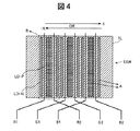
図4は図3に示した仮想タイル部分に形成されるサンプリングスイッチ回路の一つの構成を説明する拡大平面図、図5は図4の要部をさらに拡大して略帯状結晶シリコン膜の結晶方向を示す薄膜トランジスタ(TFT)のチャネル部の模式図である。仮想タイルTLはパルス変調レーザ光の走査方向x(あるいは−x)方向の走査で改質されている。仮想タイルTL中の参照符号LD−Pで示した部分はP型TFTが形成されるシリコンアイランド、LD−Nで示した部分はN型TFTが形成されるシリコンアイランドである。
【0039】
図5に示したように、シリコンアイランドLD−PおよびLD−Nの略帯状結晶シリコン膜の単結晶間に存在する粒界CBは結晶方向CGRに略同一方向となるように存在する。この結晶方向CGRと対向する位置にソース電極SD1とドレイン電極SD2がそれぞれ形成される。ソース電極SD1とドレイン電極SD2の間に流れる電流(チャネル電流)Ichの方向が結晶方向CGRと略平行する方向に設定される。このように、結晶方向CGRと電流Ichの方向を同一とすることにより、チャネルにおける電子の移動度を大きくすることができる。
【0040】
図6は図4に示した1つの仮想タイルにおけるB部分の拡大平面図、図7は図6のC−C'線に沿った断面図である。また、図8は図6の動作を説明するタイミング図である。図6と図7の構成と動作を図7および図2を参照して説明する。図6において、参照符号NT1とNT2はN型薄膜トランジスタ、PT1とPT2はP型薄膜トランジスタ、SR1+,SR1−,SR2+,SR2−はバッファBAを介して送られてきた水平シフトレジスタHSRからの信号線、VR+,VR−は赤のデータ信号(赤のビデオ信号)を示す。図7の参照符号SUB1はアクティブ・マトリクス基板、NCはN型チャネル、PCはP型チャネル、GIはゲート絶縁膜、L1は層間絶縁膜、PASSは絶縁保護膜を示す。
【0041】
図8の時刻1で信号線SR1+には“1”が、信号線SR1−には“−1”が出力され、時刻2で信号線SR2−には“−1”が、信号線SR2+には“1”が出力される。また、赤のデータ信号VR+は時刻1で画素1の信号(極性+)が、時刻2で画素2の信号(極性+)を出力する。同様に、赤のデータ信号VR−は時刻1で画素2の信号(極性−)が、時刻2で画素1の信号(極性−)を出力する。N型薄膜トランジスタNT1は時刻1にオンとなって赤のデータ信号VR+を信号線R1に出力する。P型薄膜トランジスタPT1は時刻2にオンとなって赤のデータ信号VR−を信号線R1に出力する。
【0042】
そして、N型薄膜トランジスタNT2は時刻2にオンとなって赤のデータ信号VR+を信号線R2に出力し、P型薄膜トランジスタPT2は時刻1にオンとなって赤のデータ信号VR−を信号線R2に出力する。これにより、信号線R1は時刻1に極性+のデータ(画素信号)を、時刻2に極性−のデータ(画素信号)を出力する。また、信号線R2は時刻1に極性−のデータ(画素信号)を、時刻1に極性+のデータ(画素信号)を出力する。
【0043】
以上説明した実施例では、略帯状結晶シリコン膜の仮想タイルTLをサンプリング回路SAMPを構成するサンプリングスイッチSSWの回路形成部分毎に設定した。前記したように、サンプリングスイッチSSWはアナログスイッチで構成され、回路構成が複雑で特に精細度が要求される部分である。この回路部分に仮想タイルTLで示される略帯状結晶シリコン膜を設けて薄膜トランジスタを形成することで、電子移動度が大で精細度を向上させた回路を実現することが可能となる。その結果、高速の画像表示を実現できる。なお、仮想タイルを設定する箇所は上記したサンプリング回路SAMPのみに限らず、図2に示した範囲SXの適宜の回路形成部分にも適用することができる。
【0044】
図9は本発明による画像表示装置を液晶表示装置に適用した他の実施例を模式的に説明するための図2と同様のブロック図である。本実施例は、仮想タイルTLを第1のラッチ回路LT1と第2のラッチ回路LT2の部分、デジタル−アナログ変換器DACとバッファ回路BAの部分に形成した。このように、本実施例では、仮想タイルTLをx方向に平行な2列以上に形成したものである。他の構成は図2と同様なので重複する説明は省略する。なお、ここでも、説明を容易にするため、仮想タイルTLのそれぞれを大まかな範囲で示してあるが、それぞれの仮想タイルTLは適用する回路規模に応じた適宜の大きさをもつ複数の仮想タイルをブロック化した集合体とする場合も含む。
【0045】
これらの回路部分に仮想タイルTLで示される略帯状結晶シリコン膜を設けることで、電子移動度が大で精細度を向上することが可能となる。その結果、高速で高精細の画像表示を実現できる。なお、仮想タイルを設定する箇所は上記の部分に限るものではなく、図2と同様にサンプリング回路SAMPも含めることもできる。また、仮想タイルTLを第1のラッチ回路LT1、第2のラッチ回路LT2、デジタル−アナログ変換器DAC、バッファ回路BAのそれぞれ、あるいは適宜に組合せた回路を含む種々のサイズに設定してもよい。
【0046】
上記した各実施例で説明した仮想タイルの大きさや配列、個々の改質領域の大きさや配列は、それぞれの適用回路の薄膜トランジスタの作り込みパターンを考慮して決定すればよく、例えば千鳥状の配列等も可能であり、また必ずしも規則的配列にこだわる必要はない。
【0047】
以上の実施例では、データ側の駆動回路を形成する駆動回路領域DAR1に略帯状結晶シリコン膜の不連続改質領域(仮想タイル)を適用しているが、本発明はこれに限らず、走査駆動回路領域DAR2、あるいはプリチャージ回路を有する駆動回路領域DAR3に対しても同様に適用可能である。
【0048】
このように、上記各実施例の構成によれば、マトリクス状に配置された画素部を駆動するための駆動回路に高速の移動度で動作する高性能の薄膜トランジスタ回路を有するアクティブ・マトリクス基板を備えた画像表示装置を製造することができ、高品質の画像表示装置を得ることができる。
【0049】
次に、本発明の画像表示装置の製造方法の実施例について図10乃至図15を参照して説明する。ここで説明する製造方法はCMOSの薄膜トランジスタの製造を例としており、N型薄膜トランジスタは自己整合GOLDD(Gate Overlapped Light Doped Drain)、P型薄膜トランジスタはカウンタードープによって形成する。
【0050】
図10乃至図15は一連の製造プロセスを示し、この一連の製造プロセスを図10の(A)から図15の(N)に従って説明する。先ず、アクティブ・マトリクス基板となる絶縁基板として、厚さが0.3mm乃至1.0mm程度で、好ましくは400°C乃至600°Cの熱処理で変形や収縮の少ない耐熱性のガラス基板SUB1を準備する。好ましくは、このガラス基板SUB1の上に熱的、化学的なバリア膜として機能するおよそ約50nm厚のSiN膜および約100nm厚のSiO膜をCVD法で連続かつ均一に堆積する。このガラス基板SUB1上にCVD等の手段でアモルファスシリコン膜ASIを形成する。 ・・・・・図10(A)
【0051】
次に、エキシマレーザ光ELAをx方向に走査し、アモルファスシリコン膜ASIを溶解し、結晶化してガラス基板SUB1上のアモルファスシリコン膜ASI全体を多結晶シリコン膜、すなわちポリシリコン膜PSIに改質する。 ・・・・・図10(B)
【0052】
なお、エキシマレーザ光ELAに替えて、他の方法、例えば固体パルスレーザアニールによる結晶化、シリコン膜の形成時にポリシリコン膜となるCat−CVD膜を採用することもできる。
【0053】
ホトリソグラフィー法あるいはドライエッチング法により、後述するパルス変調レーザ等のレーザ光SXL(なお、ここではパルス幅変調レーザを用いるものとして説明する)の照射位置決め等のターゲットとなる位置決めマークMKを形成する。 ・・・・・図10(C)
【0054】
マークMKを参照しながら、パルス変調レーザ光SXLをx方向に走査しながら所定の領域を選択しながら不連続で照射する。この選択的な照射でポリシリコン膜PSIを改質し、当該走査方向に連続した粒界を持つ略帯状結晶シリコン膜の不連続改質領域(仮想タイルのシリコン膜)SPSIを形成する。このとき、図1の駆動回路領域DAR1および/またはDAR2を走査するレーザ光を駆動回路領域DAR3までカバーさせることで、駆動回路領域DAR1、DAR2の隣接辺にある駆動回路領域DAR3にも同時に仮想タイルを形成することができる。 ・・・・・図11(D)
【0055】
ホトリソグラフィー法を用いて略帯状結晶シリコン膜の不連続改質領域(仮想タイルのシリコン膜)SPSIを加工し、薄膜トランジスタを作り込むアイランドSPSI−Lを形成する。 ・・・・・図11(E)
【0056】
不連続改質領域(仮想タイルのシリコン膜)SPSIのアイランドSPSI−Lを覆ってゲート絶縁膜GIを形成する。 ・・・・・図11(F)
【0057】
N型薄膜トランジスタを形成する領域に閾値を制御するためのインプランテーションNEを行う。このとき、P型薄膜トランジスタを形成する領域をホトレジストRNEで覆う。 ・・・・・図12(G)
【0058】
次に、P型薄膜トランジスタを形成する領域に閾値を制御するためのインプランテーションPEを行う。このとき、P型薄膜トランジスタを形成する領域をホトレジストRPEで覆う。 ・・・・・図12(H)
【0059】
この上に、スパッタリング法またはCVD法を用いて薄膜トランジスタのゲート電極となる二層の金属ゲート膜GT1,GT2を形成する。
・・・・・図12(I)
【0060】
金属ゲート膜GT1,GT2の形成領域をホトレジストRNで覆い、ホトリソグラフィー法により、金属ゲート膜GT1,GT2をパターニングする。このとき、LDD領域を形成するため、上層の金属ゲート膜GT2を所要量サイドエッチングし、下層の金属ゲート膜GT1より後退させる。この状態で、ホトレジストRNをマスクとしてN型の不純物Nをインプランテーションし、N型薄膜トランジスタのソース・ドレイン領域NSDを形成する。 ・・・・・図13(J)
【0061】
ホトレジストRNを剥離し、金属ゲート膜GT2をマスクとしてインプランテーションLDDを行い、N型薄膜トランジスタのLDD領域NLDDを形成する。 ・・・・・図13(K)
【0062】
N型薄膜トランジスタの形成領域をホトレジストRPで覆い、P型薄膜トランジスタのソース・ドレイン形成領域にP型の不純物Pをインプランテーションし、P型薄膜トランジスタのソース・ドレイン領域PSDを形成する。 ・・・・・図14(L)
【0063】
ホトレジストRPを剥離し、インプランテーションによる不純物を活性化した後、CVD法等で層間絶縁膜LIを形成する。 ・・・・・図14(M)
【0064】
ホトリソグラフィー法により層間絶縁膜LIとゲート絶縁膜GIにコンタクトホールを形成し、このコンタクトホールを介してN型薄膜トランジスタとP型薄膜トランジスタの各ソース・ドレインNSD、PSDに配線用の金属層を接続し、配線Lを形成する。この上に、層間絶縁膜L2を形成し、さらに保護絶縁膜PASSを形成する。 ・・・・・図14(N)
【0065】
以上の工程により、略帯状結晶シリコン膜の不連続改質領域(仮想タイルのシリコン膜)SPSIにCMOS薄膜トランジスタが形成される。なお一般に、N型薄膜トランジスタは劣化が激しい。チャネルとソース・ドレイン領域との間に低濃度不純物領域LDD(Light Doped Drain領域)を形成すると、この劣化が緩和される。GOLDDは低濃度不純物領域にゲート電極が被さった構造を有している。この場合、LDDで観測される性能低下が緩和される。P型薄膜トランジスタでは、その劣化がN型薄膜トランジスタほど深刻でなく、低濃度不純物領域LDDやGOLDDは通常は採用されない。
【0066】
次に、本発明の特徴である略帯状結晶シリコン膜の不連続改質領域(仮想タイルのシリコン膜)の形成について図16乃至図26を参照して説明する。図16は略帯状結晶シリコン膜の不連続改質領域(仮想タイルのシリコン膜)の形成プロセスの説明図であり、同図(a)はプロセスを説明する模式図、同図(b)はパルス変調レーザの波形例、同図(c)は擬似CWレーザの波形例を示す。
【0067】
略帯状結晶シリコン膜の不連続改質領域(仮想タイル)は、絶縁基板SUB1に有するバッファ層BFL上に形成されたポリシリコン膜PSIに図16の(b)又は(c)に示したレーザ光SXLを照射することで得られる。レーザ光SXLは(b)のパルス変調レーザ光、又は(c)に示したような擬似CWレーザ光を10ns乃至100msの周期で照射する。このレーザ光SXLを図16(a)に示したようにポリシリコン膜PSI上をx方向に走査し、y方向にシフトさせた後に−x方向に走査することで、当該走査方向x、−x方向に略帯状結晶を有するシリコン膜SPSIが得られる。絶縁基板SUNB1には位置決めのためのマークMKを有し、このマークMKを位置決めターゲットとしてレーザ光SXLの走査を行う。このように断続的にレーザを照射しながら基板を走査するので、略帯状結晶のシリコン膜SPSIを仮想タイル状に配列することができる。
【0068】
図17は略帯状結晶シリコン膜の結晶構造の説明図であり、同図(a)はレーザ光SXLの走査態様を説明する模式図、同図(b)はレーザ光SXLの走査により形成された略帯状結晶シリコン膜SPSIを非走査部分に残留するポリシリコン膜PSIとの結晶構造の違いを比較して示す模式図である。ポリシリコン膜PSIを同図(a)のようにレーザ光SXLの走査で改質することで、同図(b)に示したように、単結晶がレーザ光の走査方向に帯状に延在する略帯状結晶シリコン膜SPSIの結晶構造となる。参照符号CBは粒界を示す。
【0069】
略帯状結晶シリコン膜SPSIの平均粒サイズはレーザ光SXLの走査方向に約5μm程度、走査方向と直角方向(粒界CB間の幅)に0.5μm程度となる。なお、走査方向の粒サイズはレーザ光SXLのエネルギーや走査速度、パルス幅等の条件で可変である。これに対し、ポリシリコン膜PSIの平均粒径は0.6μm(0.3乃至1.2μm)程度である。このような結晶構造の相違によって、ポリシリコン膜PSIと略帯状結晶シリコン膜SPSIとを用いて薄膜トランジスタを構成した場合の電子移動度に大きな差をもたらす。
【0070】
上記の略帯状結晶シリコン膜SPSIは、下記の特徴を有する。すなわち、
(a)表面に対する主配向が{110}である。
【0071】
(b)キャリアの移動方向に略垂直な面の主配向が{100}である。
【0072】
上記(a)、(b)の2つの方位は、電子線回折法あるいはEBSP(Electron Backscatter Diffraction Pattern)法により評価できる。
【0073】
(c)膜の欠陥密度が1×1017cm-3より小さい。膜中の結晶欠陥数は、電気的特性、あるいは電子スピン共鳴(ESR)による不対電子の定量的評価から定義される値である。
【0074】
(d)膜のホール移動度が50cm2 /Vs以上、700cm2 /Vs以下である。
【0075】
(e)膜の熱伝導率は、温度依存性があり、ある温度で最大値を示す。熱伝導率は温度が上昇すると一端上昇し、最大値50W/mK以上、100W/mK以下の値を示す。高温領域では、熱伝導率は温度上昇に伴い低下する。熱伝導率は、3オメガ方法などから評価、定義される値である。
【0076】
(f)薄膜のラマン散乱分光から評価、定義されるラマンシフトは、512cm-1以上、518cm-1以下である。
【0077】
(g)膜の結晶粒界のΣ値の分布は、Σ11に最大値を有し、ガウス型に分布する。なお、Σ値は電子線回折法あるいはEBSP(Electron Backscatter Diffraction Pattern法から計測される値である。
【0078】
(h)膜の光学定数は、下記の条件を満たす領域であることを特徴とする。波長500nmにおける屈折率nは2.0以上、4.0以下であり、かつ減衰係数kは0.3以上、1以下であること。さらに、波長300nmにおける屈折率nは3.0以上、4.0以下であり、かつ減衰係数kは3.5以上、4以下であること。なお、光学定数は、分光エリプソメータによって計測された値である。
【0079】
図18はシリコン膜の結晶構造の相違に起因する薄膜トランジスタのチャネルにおける電子移動度の相違の説明図である。同図(a)は薄膜トランジスタのチャネル構造と当該チャネル部分のシリコン膜SIの粒界CBと電子移動の関係を示し、同図(b)はソースSD1とドレインSD2間に流れる電流が横断する粒界数と電子移動度の関係を示す。シリコン膜SIがポリシリコン膜PSIの場合はドレインSD2からソースSD1に電流が横断する粒界数が多く、シリコン膜SIが略帯状結晶シリコン膜SPSIの場合は大きな単結晶が成長方向に長く存在し、横断する粒界数が少ない。この関係を図18(b)に示した。
【0080】
平均横断粒界数Cは、電流方向でチャネルの幅をj分割し、電流が流れる方向で横断する粒界数をNiとしたとき、C=ΣNi/jで表される。図18(b)には、横軸に平均横断粒界数を、縦軸に電子移動度(cm2 /V・s)とその逆数(V・s/cm2 )を取って示してある。このように、薄膜トランジスタのチャネルを構成する略帯状結晶シリコン膜SPSIの結晶成長方向に電流が流れるようにソースSD1とドレインSD2を配置することにより、電子移動度は極端に大きくなる。すなわち、薄膜トランジスタの動作速度が大きくなる。したがって、薄膜トランジスタ自体を精細に作り込むことが可能となり、図3で説明したように、画素ピッチに対して配線R1,G1,B1,R2,G2,B2を狭いピッチで形成することができる。その結果、仮想タイルを用いて形成した回路間には大きなスペースが生じる。このスペースを他の配線等の形成スペースに利用することも可能である。
【0081】
図19はレーザ光の照射装置の一例を説明する構成図である。この照射装置ではポリシリコン膜PSIを形成したガラス基板SUB1をx−y方向の駆動ステージXYT上に設置し、基準位置測定用カメラCMを用いて位置合わせを行う。基準位置測定信号POSは制御装置CRLに入力され、駆動設備MDに入力された制御信号CSに基づいて照射位置の微調整を行い、所定の速度でステージXYTを移動させて一方向(図1のx方向)に走査する。かかる走査に同期して照射設備LUからレーザ光SXLをポリシリコン膜PSIに照射して、略帯状結晶シリコン膜SPSIに改質する。
【0082】
照射設備LU内には一例として連続発振(CW)固体レーザLS(レーザダイオード)励起の発振器、ホモジナイザ、パルス幅を変調するためのEOモジュレータ等の光学系HOS、反射ミラーML、集光レンズ系LZを配置することで所望の照射ビームを形成できる。レーザ光SXLの照射時間、照射強度などは制御装置CRLからのON−OFF信号SWS、制御信号LECで調整する。
【0083】
図20は仮想タイルのレイアウトの一例を説明する平面図である。この配置例では、仮想タイルTLは図1で説明した駆動回路領域DAR1に複数列で配置されている。仮想タイルTLは作り込む回路パルスに応じて、1列、2以上の多列、あるいは千鳥状等に配列することができる。本例では、3列(または、3段)としてある。各仮想タイルTLのサイズは、x方向の長さwが20μm以上で1mm以下、y方向の幅hが20μm以上で1mm以下、x方向に隣接する仮想タイルとの間隔dが3μm以上、y方向の間隔pが3μm以上となっている。この配置サイズはレーザのパワー、高品質な結晶を安定して成長させることができるサイズによって制約される。
【0084】
図21は図19の照射装置を用いたレーザ照射プロセス例の説明図である。図21では絶縁基板を単に基板と表記する。先ず、ポリシリコン膜を形成した絶縁基板にレーザ光SXLを照射するため、装置電源をONとし、レーザ発振器をONとする。駆動ステージXYT上に絶縁基板をセットし、真空チャックで固定する。絶縁基板の位置決めマークをターゲットとしてX軸、Y軸、およびθ軸(X−Y平面での回転方向)を規定値に調整し、絶縁基板の準備を完了する。
【0085】
一方、照射装置に各種条件を入力し、確認を行う。条件入力項目は、レーザ出力(NDフィルタの調整等)、結晶化位置(駆動ステージXYT上)のセット位置、結晶化距離(仮想タイルの結晶成長方向長さ)、間隔(仮想タイルの間隔)、個数(仮想タイルの作成個数)、レーザ光路上にあるスリット幅の調整、対物レンズのセット等である。結晶化距離、間隔、個数はEOモジュレータにセットする。また、確認事項は、レーザ光のビームプロファイラ、パワーモニタ、レーザ光照射位置等である。
【0086】
絶縁基板の準備が完了し、条件入力と確認が取られた後、絶縁基板の表面高さを測定し、オートフォーカス機構を作動させてレーザ光を照射する。レーザ光の照射でオートフォーカス機構を補正し、絶縁基板の表面高さを制御する。また、レーザ光の照射を継続中に絶縁基板の走査距離と照射位置を条件入力側にフィードバックする。
【0087】
所定の領域にレーザ光の照射処理を完了後、真空チャックをOFFとして駆動ステージXYTから絶縁基板を取り出す。以下、次の絶縁基板を駆動ステージXYTにセットし、上記操作を必要回数繰り返す。全ての必要な絶縁基板のレーザ照射処理を完了したとき、レーザ発振器をOFFとし、装置電源をOFFして終了する。
【0088】
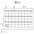
図22は多面取りの大サイズ素材絶縁基板上における各個別の絶縁基板に対する略帯状結晶シリコン膜SPSIの仮想タイル形成操作の説明図である。図22中、参照符号M−SUBは大サイズ素材絶縁基板で、この大サイズ素材絶縁基板M−SUBに個々の画像表示装置のアクティブ・マトリクス基板SUB1が多数形成されている。ここでは、8×6=48枚取りとして示したが、これに限らないことは言うまでもない。この大サイズ素材絶縁基板M−SUBの駆動回路領域に対して、マークMKをターゲットとした位置合わせ後、レーザ光を図中に矢印SDSで示したように往復走査する。ここでは、3本のレーザ光を並列の走査することで、短時間に大サイズの素材絶縁基板M−SUBに所要の仮想タイルを形成できるようにしている。
【0089】
図23は図22で形成した仮想タイルの位置の一例を説明する一枚のアクティブ・マトリクス基板の平面図であり、同図(a)は全体図、同図(b)は同図(a)の矢印A部分の拡大図である。この例では、アクティブ・マトリクス基板SUB1のデータ信号の駆動回路領域DAR1を形成するx方向の一辺に複数の仮想タイルTLのブロックを一列に配置してある。この場合、仮想タイルは図2あるいは図9に参照符号SXで示した全域、または図2のサンプリング回路SAMP部分、図9の各ラッチ回路LT1、LT2の部分とデジタル−アナログ変換器DACやバッファ回路BAの部分に複数個設け、これをブロックに分けて配置する。仮想タイルを構成する個々の改質領域も同様に配置される。なお、同図(b)の仮想タイルのブロックや個々の改質領域の大きさや位置は本発明を分かり易く示したもので、実際の回路の大きさや位置とは異なる。
【0090】
図24は仮想タイルの他の配列を説明する図23(b)と同様の拡大図である。仮想タイルTLのブロックは同図(a)のようにx方向に平行な二列に配置され、あるいは同図(b)のようにx方向に平行で互いに千鳥状の三列に配置される。なお、各ブロックの大きさ、間隔は適用する回路構造に対応して可変とすることが可能である。なおブロックを構成する個々の改質領域の配列も複数配列、あるいは千鳥状の配列にすることができる。
【0091】
図25と図26は仮想タイルの位置の他例を説明する一枚のアクティブ・マトリクス基板の平面図である。図25では図1で説明した駆動回路領域DAR1とDAR3に仮想タイルを適用したものである。また、図26では図1で説明した駆動回路領域DAR1とDAR3およびアクティブ・マトリクス基板SUB1のy方向に延びる一辺に形成した走査駆動回路領域DAR2に仮想タイルを適用したものである。個々の仮想タイルやブロックの配列等は図23乃至図24で説明したものと同様である。
【0092】
次に、絶縁基板(アクティブ・マトリクス基板)に仮想タイルを形成するための位置決め用のマークについて説明する。図27はアクティブ・マトリクス基板SUB1への位置決め用のマーク付けとこのマークをターゲットとしたレーザの照射プロセスの第1例の説明図である。この例では、アクティブ・マトリクス基板SUB1に形成されているシリコン膜SIにホトリソグラフィー法で位置決め用のマークMKを形成し(P−1)、その後の連続パルスレーザSLXの照射時にこのマークMKを基準として位置決め(アライメント)を取る(P−2)。そして同様に、このマークMKを基準として連続パルスレーザSLXの照射で改質された略帯状結晶シリコン膜SPSIをアイランドSPSI−Lに加工する(P−3)。なお、このマークMKはアモルファスシリコン膜ASIの段階で形成してもよく、またポリシリコン膜の段階で形成してもよい。
【0093】
図28はアクティブ・マトリクス基板SUB1への位置決め用のマーク付けとこのマークをターゲットとしたレーザ光の照射プロセスの第2例の説明図である。この例では、アクティブ・マトリクスSUB1にポリシリコン膜PSIを形成後(P−1)、ポリシリコン膜PSIにレーザSLXを照射する際に、当該レーザSLXで位置決め用のマークMKを形成するようにしたものである(P−2)。その後のアイランドSPSI−Lの形成時にこのマークMKで位置決めを行う(P−3)。
【0094】
ポリシリコン膜PSIと略帯状結晶シリコン膜SPSIとは可視光の反射率に差がある。この差を位置決めターゲットとして利用することができる。また、ポリシリコン膜PSIと略帯状結晶シリコン膜SPSIとは、結晶の大きさに起因して高さに相違がでて来る。この略帯状結晶化したマークMKの部分の結晶粒界の段差をターゲットとして利用することもできる。なお、マークMK部分のポリシリコン膜をレーザアブレーションで除去してマークMKとすることもできる。このレーザアブレーションによるマークMKの形成方法は、マークMK形成のためのホトリソグラフィー工程を省略できる利点がある。
【0095】
図29はアクティブ・マトリクス基板SUB1への位置決め用のマーク付けとこのマークをターゲットとしたレーザ光の照射プロセスの第3例の説明図である。この例では、アクティブ・マトリクス基板SUB1にシリコン膜を形成する前に当該ガラス基板または下地膜に予めエッチング法あるいは機械的手段でマークMKを形成する(P−1)。アクティブ・マトリクス基板SUB1にポリシリコン膜PSIを形成し、このマークMKを基準としてレーザ光SLXを照射して略帯状結晶シリコン膜SPSIを形成する(P−2)。その後のアイランドSPSI−Lの形成時にこのマークMKで位置決めを行う(P−3)。
【0096】
上記したように、本実施例によれば、ポリシリコン膜をさらに大きな結晶に改質し、その結晶成長方向の配置により、ソースとドレイン間の電流が粒界を横切る確率を低減できる。その結果、薄膜トランジスタの動作速度を向上して最良の薄膜トランジスタ回路を得ることが可能となる。そして、画像表示装置の駆動回路部分に略帯状結晶シリコン膜の半導体膜を用いた薄膜トランジスタ回路を配置することができる。本実施例で得られる薄膜トランジスタの性能は、例えばNチャンネルMISトランジスタを作成する場合に、電界効果移動度が約300cm2 /V・s以上でかつ、閾値電圧のバラツキを±0.2V以下に抑制することができ、高性能、高信頼で動作し、デバイス間の均一性が優れたアクティブ・マトリクス基板を用いた表示装置を製造することができる。
【0097】
また本実施例では、電子キャリアを付与するリンのイオン打ち込みに代えてホールキャリアを付与するボロン打ち込みによりPチャンネルMISトランジスタを製造することもできる。また、上記したCMOS型の回路では周波数特性の向上が期待でき、高速動作に適している。
【0098】
図30は本発明の画像表示装置の第1例としての液晶表示装置の構成を説明する展開斜視図である。また、図31は図30のZ−Z線方向で切断した断面図である。この液晶表示装置は前記したアクティブ・マトリクス基板を用いて液晶表示装置を製造する。図30と図31において、参照符号PNLはアクティブ・マトリクス基板SUB1とカラーフィルタ基板SUB2の貼り合わせ間隙に液晶を封入した液晶セルで、その表裏に偏光板POL1,POL2が積層されている。また、参照符号OPSは拡散シートやプリズムシートからなる光学補償部材、GLBは導光板、CFLは冷陰極蛍光ランプ、RFSは反射シート、LFSはランプ反射シート、SHDはシールドフレーム、MDLはモールドケースである。
【0099】
前記した実施例の何れかの構成を有するアクティブ・マトリクス基板SUB1上に液晶配向膜層を形成し、これにラビング等の手法で配向規制力を付与する。画素領域ARの周辺にシール剤を形成した後、同様に配向膜層を形成したカラーフィルタ基板SUB2を所定のギャップで対向配置させ、このギャップ内に液晶を封入し、シール剤の封入口を封止材で閉鎖する。こうして構成した液晶セルPNLの表裏に偏光板POL1,POL2を積層し、導光板GLBと冷陰極蛍光ランプCFL等からなるバックライト等を光学補償部材OPSを介して実装することで液晶表示装置を製造する。なお、液晶セルの周辺に有する駆動回路にはフレキシブルプリント基板FPC1,FPC2を介してデータやタイミング信号が供給される。参照符号PCBは外部信号源と各フレキシブルプリント基板FPC1,FPC2の間において、当該外部信号源から入力する表示信号を液晶表示装置で表示する信号形式に変換するタイミングコンバータ等が搭載されている。
【0100】
本実施例のアクティブ・マトリクス基板を使用した液晶表示装置は、その画素回路に上記した優れたポリシリコン薄膜トランジスタ回路を配置することで、電流駆動能力に優れることから高速動作に適している。さらに、閾値電圧のバラツキが小さいために画質の均一性に優れ液晶表示装置を安価に提供できるのが特長である。
【0101】
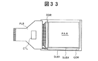
また、本実施例のアクティブ・マトリクス基板を用いて有機EL表示装置を製造することができる。図32は本発明の画像表示装置の第2例としての有機EL表示装置の構成例を説明する展開斜視図である。また、図33は図32に示された構成要素を一体化した有機EL表示装置の平面図である。前記した各実施例の何れかのアクティブ・マトリクス基板SUB1に有する画素電極上に有機EL素子を形成する。有機EL素子は、画素電極表面から順次、ホール輸送層、発光層、電子輸送層、陰極金属層などを蒸着した積層体から構成される。このような積層層を形成したアクティブ・マトリクス基板SUB1の画素領域PARの周囲にシール材を配置し、封止基板SUBXまたは封止缶で封止する。
【0102】
この有機EL表示装置は、その駆動回路領域DDR、に外部信号源からの表示用信号をプリント基板PLBで供給する。このプリント基板PLBにはインターフェース回路チップCTLが搭載されている。そして、上側ケースであるシールドフレームSHDと下側ケースCASで一体化して有機EL表示装置とする。
【0103】
有機EL表示装置用のアクティブ・マトリクス駆動では、有機EL素子が電流駆動発光方式であるために高性能の画素回路の採用が良質な画像の提供には必須であり、CMOS型薄膜トランジスタの画素回路を用いるのが望ましい。また、駆動回路領域に形成する薄膜トランジスタ回路も高速、高精細化には必須である。本実施例のアクティブ・マトリクス基板SUB1は、このような要求を満たす高い性能を有している。本実施例の製造方法で製造したアクティブ・マトリクス基板を用いた有機EL表示装置は本実施例の特長を最大限に発揮する表示装置の1つである。
【0104】
本発明の製造方法は上記した画像表示装置のアクティブ・マトリクス基板に限るものではなく、また、本発明の製造方法は特許請求の範囲に記載の構成および実施例に記載の構成に限定されるものではなく、本発明の技術思想を逸脱することなく種々の変更が可能であり、例えば各種の半導体装置の製造にも適用することもできる。
【0105】
【発明の効果】
以上説明したように、本発明はアクティブ・マトリクス基板の画素領域の周辺に配置される駆動回路領域の回路を構成するシリコン膜にパルス変調レーザ光あるいは擬似CWレーザ光を照射して選択的に改質された略帯状結晶シリコン膜の不連続改質領域を形成し、この不連続改質領域に薄膜トランジスタ等のアクティブ素子からなる駆動回路を形成するという新規な方法を採用することにより、高速の移動度で動作する高性能の画像表示装置を得ることができる。
【図面の簡単な説明】
【図1】本発明による製造方法を適用して製造した画像表示装置の一例としての液晶表示装置を模式的に説明するための平面図である。
【図2】図1におけるデータ駆動回路部分の回路構成例を説明するブロック図である。
【図3】図2におけるサンプリング回路を構成するサンプリングスイッチ部分の構成図である。
【図4】図3に示した仮想タイルに形成されるサンプリングスイッチ回路の一つの構成を説明する拡大平面図である。
【図5】図4の要部をさらに拡大して略帯状結晶シリコン膜の結晶方向を示す薄膜トランジスタ(TFT)のチャネル部の模式図である。
【図6】図4に示した1つの仮想タイルにおけるB部分の拡大平面図である。
【図7】図6のC−C’線に沿った断面図である。
【図8】図6の動作を説明するタイミング図である。
【図9】本発明による画像表示装置を液晶表示装置に適用した他の実施例を模式的に説明するための図2と同様のブロック図である。
【図10】本発明の画像表示装置の製造方法の一実施例を説明するプロセスの説明図である。
【図11】本発明の画像表示装置の製造方法の一実施例を説明する図10に続くプロセスの説明図である。
【図12】本発明の画像表示装置の製造方法の一実施例を説明する図11に続くプロセスの説明図である。
【図13】本発明の画像表示装置の製造方法の一実施例を説明する図12に続くプロセスの説明図である。
【図14】本発明の画像表示装置の製造方法の一実施例を説明する図13に続くプロセスの説明図である。
【図15】本発明の画像表示装置の製造方法の一実施例を説明する図14に続くプロセスの説明図である。
【図16】略帯状結晶シリコン膜の不連続改質領域(仮想タイル)の形成プロセスの説明図である。
【図17】略帯状結晶シリコン膜の結晶構造の説明図である。
【図18】シリコン膜の結晶構造の相違に起因する薄膜トランジスタのチャネルにおける電子移動度の相違の説明図である。
【図19】レーザ光の照射装置の一例を説明する構成図である。
【図20】仮想タイルのレイアウトの一例を説明する平面図である。
【図21】図19の照射装置を用いたレーザ照射プロセス例の説明図である。
【図22】多面取りの大サイズ素材絶縁基板上における各個別の絶縁基板に対する略帯状結晶シリコン膜SPSIの仮想タイル形成操作の説明図である。
【図23】図22で形成した仮想タイルの位置の一例を説明する一個のアクティブ・マトリクス基板の平面図である。
【図24】仮想タイルの他の配列を説明する図23(b)と同様の拡大図である。
【図25】仮想タイルの位置の他例を説明する一個のアクティブ・マトリクス基板の平面図である。
【図26】仮想タイルの位置のさらに他例を説明する一個のアクティブ・マトリクス基板の平面図である。
【図27】アクティブ・マトリクス基板への位置決め用のマーク付けとこのマークをターゲットとした連続パルスレーザの照射プロセスの第1例の説明図である。
【図28】アクティブ・マトリクス基板SUB1への位置決め用のマーク付けとこのマークをターゲットとした連続パルスレーザの照射プロセスの第2例の説明図である。
【図29】アクティブ・マトリクス基板SUB1への位置決め用のマーク付けとこのマークをターゲットとした連続パルスレーザの照射プロセスの第3例の説明図である。
【図30】本発明の画像表示装置の第1例としての液晶表示装置の構成を説明する展開斜視図である。
【図31】図30のZ−Z線方向で切断した断面図である。
【図32】本発明の画像表示装置の第2例としての有機EL表示装置の構成例を説明する展開斜視図である。
【図33】図32に示された構成要素を一体化した有機EL表示装置の平面図である。
【図34】一般的なエキシマパルスレーザ光照射を走査することによるアモルファスシリコン膜の結晶化方法の説明図である。
【図35】図34におけるレーザ光照射部の部分平面図と薄膜トランジスタ部の構成例を説明する要部平面図である。
【符号の説明】
SUB1・・・・アクティブ・マトリクス基板、PAR・・・・画素領域、DAR1、DAR2、DAR3・・・・駆動回路領域、DDR1、DDR2、・・・・・DDRn−1、DDRn・・・・データ駆動回路、GDR1、GDR2・・・・走査回路、SUB2・・・・カラーフィルタ基板、CPADQ・・・・パッド、HSR・・・・水平シフトレジスタ、LT1・・・・第1ラッチ回路、LTS・・・・第2ラッチ回路、DAC・・・・デジタル−アナログ変換器、BA・・・・バッファ回路、SAMP・・・・サンプリング回路、VSR・・・・垂直シフトレジスタ、R1,G1,B1,R2,G2,B2・・・・信号線、TL・・・・仮想タイル、ELA・・・・エキシマレーザ光、SXL・・・・パルス変調レーザ光あるいは擬似CWレーザ光、SPSI・・・・略帯状結晶シリコン膜の不連続改質領域(仮想タイルのシリコン膜)、ASI・・・・アモルファスシリコン膜、PSI・・・・ポリシリコン膜。[0001]
BACKGROUND OF THE INVENTION
The present invention relates to an image display device, and more particularly to an image display device in which a crystal structure of a semiconductor film formed on an insulating substrate is modified with laser light, and an active element of a drive circuit is formed on the modified semiconductor film. It relates to a manufacturing method.
[0002]
[Prior art]
2. Description of the Related Art An active matrix display device (or an active matrix drive image display device, or simply a display device) using active elements such as thin film transistors as a driving element for pixels arranged in a matrix is widely used. Many image display devices of this type are arranged by arranging a large number of pixel circuits and drive circuits formed of active elements such as thin film transistors (TFTs) formed using a silicon film as a semiconductor film on an insulating substrate. A high-quality image can be displayed. Here, a thin film transistor which is a typical example of the active element will be described as an example.
[0003]
In a thin film transistor using an amorphous silicon semiconductor film (amorphous silicon semiconductor film) that has been generally used as a semiconductor film, there is a limit to the performance of the thin film transistor represented by its carrier (electron or hole) mobility. Therefore, it has been difficult to construct a circuit that requires high speed and high functionality. In order to realize a high mobility thin film transistor necessary to provide better image quality, an amorphous silicon film (hereinafter also referred to as an amorphous silicon film) is preliminarily formed into a polysilicon film (hereinafter also referred to as a polycrystalline silicon film). It is effective to form (thinner) the thin film transistor using a polysilicon film. For this modification, a technique of annealing the amorphous silicon film by irradiating laser light such as excimer laser light is used.
[0004]
For example, TCAngelis et al; Effect of Excimer Laser Annealing on the Structural and Electrical Properties of Polycrystalline Silicon Thin-Film Transistor, J. Appl. Phy., Vol. 86, pp4600-4606, 1999. Or H. Kuriyama et al; Lateral Grain Growth of Poly-Si Films with a Specific Orientation by an Eximer Laser Annealing Method, Jpn.J.Appl.Phy., Vol.32, pp6190-6195,1993 or K.Suzuki et al Correlation between Power Density Fluctuation and Grain Size Distribution of Laser annealed Poly-Crystalline Silicon, SPIE Conference, Vol.3618, pp310-319, 1999.
[0005]
A modification method by crystallization of an amorphous silicon film using excimer laser light irradiation will be described with reference to FIG. FIG. 34 is an explanatory view of a method for crystallizing an amorphous silicon film by scanning the most general excimer pulse laser beam irradiation. FIG. 34 (a) shows the configuration of an insulating substrate on which an irradiated semiconductor layer is formed. (B) shows a state modified by laser light irradiation. Glass or ceramics is used for this insulating substrate.
[0006]
In FIG. 34, an amorphous silicon film ASI deposited on an insulating substrate SUB via a base film (SiN or the like, not shown) is irradiated with a linear excimer laser beam ELA having a width of several nanometers to several hundred nanometers. As shown in FIG. 4, the amorphous silicon film ASI is annealed by performing scanning that moves the irradiation position every one to several pulses along one direction (x direction), and the amorphous silicon film ASI of the entire insulating substrate SUB is changed to polysilicon. Modification to film PSI. The polysilicon film PSI modified by this method is subjected to various processes such as etching, wiring formation, and ion implantation to form a circuit having an active element such as a thin film transistor in each pixel portion or driving portion. An active matrix type image display device such as a liquid crystal display device or an organic EL display device is manufactured using this insulating substrate.
[0007]
FIG. 35 is a partial plan view of the laser beam irradiation part in FIG. As shown in FIG. 35A, a large number of crystallized silicon particles (polycrystalline silicon) PSI of about 0.05 to 0.5 μm grow uniformly in the plane in the laser beam irradiation portion. Most of the grain boundaries of each silicon particle (that is, silicon crystal) are closed by themselves (there is a grain boundary between adjacent silicon particles in all directions). In FIG. 35A, a portion surrounded by a square is a transistor portion TRA that becomes a semiconductor film for an active element such as an individual thin film transistor. The conventional modification of the silicon film means such crystallization.
[0008]
In order to use the modified silicon film (polysilicon film PSI) to form a pixel circuit, as shown in FIG. 35B, a portion of the crystallized silicon is used as a transistor portion. Unnecessary portions other than the portion to be the transistor portion TRA in FIG. 35A are removed by etching to form an island (island) of a silicon film, and a gate insulating film (not shown) and gate are formed on the island PSI-L. A thin film transistor is manufactured by arranging the electrode GT, the source electrode SD1, and the drain electrode SD2.
[0009]
[Problems to be solved by the invention]
In the above prior art, a thin film transistor is formed on a modified polysilicon film on an insulating substrate and an active element such as a thin film transistor having good operation performance is disposed. For example, there is a limit to the carrier mobility (electron mobility or hole mobility, hereinafter also simply referred to as electron mobility) in the channel of a thin film transistor using the above. That is, the grain boundaries of the polysilicon film crystallized by the excimer laser light irradiation are closed for each individual crystal as shown in FIG. 34, and in the channel between the source electrode and the drain electrode. There is a limit to achieving greater carrier mobility. With the recent high definition, the circuit density of the drive circuit has become dense. An active element such as a thin film transistor having a very high circuit density in such a drive circuit is required to have a higher carrier mobility.
[0010]
SUMMARY OF THE INVENTION An object of the present invention is to provide a method for manufacturing an image display device including an active matrix substrate having a high-performance thin film transistor circuit or the like that operates with high-speed mobility in a driving element for driving pixel portions arranged in a matrix. Is to provide. The present invention is not limited to the modification of a polysilicon semiconductor film formed on an insulating substrate for an image display device, but to the modification of a similar semiconductor film formed on another substrate such as a silicon wafer. Can be applied similarly.
[0011]
[Means for Solving the Problems]
As means for solving the above-mentioned problems, the present invention has modified the polysilicon film by irradiating the entire surface of the amorphous silicon film formed on the entire area of the insulating substrate with the excimer laser beam, or formed the polysilicon film. An insulating substrate is prepared, and a predetermined direction is applied while selectively irradiating a polysilicon film in a drive circuit region disposed around the pixel region of the insulating substrate with a pulse modulated laser beam or a pseudo CW laser beam using a solid laser. In this way, a discontinuous modified region of a substantially band-shaped crystalline silicon film having a large crystal size modified so that crystals grown in the scanning direction have continuous grain boundaries is formed.
[0012]
The discontinuous reforming region is generally rectangular, and when a required circuit such as a drive circuit is formed in the rectangular discontinuous reforming region, the channel direction of the active elements such as thin film transistors constituting the circuit is It is made to be substantially parallel to the grain boundary direction of the substantially band-like crystalline silicon film. In the present invention, a method for creating a discontinuous modified region of a substantially band-shaped crystalline silicon film by irradiation with the above-described pulse-modulated laser light is referred to as SELAX (Selective Enhancing Laser Crystallization).
[0013]
In the manufacture of the image display device according to the present invention, preferably, the SELAX for selectively irradiating the polysilicon film of the drive circuit portion with a laser beam (hereinafter also referred to as laser light or simply laser) using a reciprocating operation. A discontinuous modified region of the substantially band-shaped crystalline silicon film is formed by the treatment. Although the discontinuous reforming region can be formed in the entire region of the drive circuit region, it is recommended that the discontinuous reforming region be formed in a substantially rectangular shape in a necessary region in consideration of the circuit density of the drive circuit. In particular, by forming the substantially rectangular discontinuous modified region mainly in the necessary region of the drive circuit region, the efficiency of the laser light irradiation treatment and the film quality of each substantially band-like crystalline silicon film are all improved. Uniformity in the discontinuous reforming region.
[0014]
The substantially band-like crystalline silicon film according to the present invention has a width in the direction perpendicular to the scanning direction of the laser beam and the length in the scanning direction, for example, a width of about 0.1 μm to 10 μm and a length of about 1 μm to 100 μm. It is an aggregate of crystals. Good carrier mobility can be secured by using such a substantially band-like crystalline silicon film. The value is about 300 cm as electron mobility. 2 / V · s or more, preferably 500cm 2 / V · s or more.
[0015]
On the other hand, in the modification of a silicon film using a conventional excimer laser, a large number of crystallized silicon particles (polysilicon) of about 0.05 μm to 0.5 μm grow randomly in the laser light irradiation portion. The electron mobility of such a polysilicon film is about 200 cm. 2 / V ・ s or less, 120cm on average 2 / V · s. This is 1 cm which is the electron mobility of the amorphous silicon film. 2 Although the performance is improved as compared with / V · s or less, the discontinuous modified region formed of the substantially band-like crystalline silicon film of the present invention has a higher electron mobility than the above-described electron mobility.
[0016]
The silicon film in the pixel region of the insulating substrate constituting the image display device according to the present invention is a polysilicon film obtained by modifying an amorphous silicon film formed by a CVD method or a sputtering method by irradiation with an excimer laser beam, and a drive circuit region. The silicon film is a substantially band-like crystalline silicon film whose crystal structure is further modified by irradiation of a pulse modulated laser beam using a solid laser or a pseudo CW laser beam on a polysilicon film. The pulse modulation referred to here means a modulation method for changing a pulse width or a pulse-to-pulse interval, or both. Specifically, such a modulated pulse can be obtained by electro-optic modulation (Electro-Optic modulation: EO modulation) of a CW (continuous oscillation) laser.
[0017]
In the present invention, by selectively irradiating the polysilicon film in the drive circuit area on the insulating substrate while scanning with the pulse modulated laser beam, the area is selectively irradiated, that is, the band-shaped crystalline silicon film is modified. The regions are formed in a substantially rectangular array along the insulating substrate surface. Hereinafter, the substantially rectangular area is also referred to as a virtual tile. The virtual tiles and the individual modified regions constituting the virtual tiles are arranged in blocks for each of the plurality of circuit areas formed thereafter. By adopting such virtual tiles, in addition to the effects described above, it is not necessary to irradiate laser light to the region of the semiconductor film that is removed by etching in the process of forming a thin film transistor or the like, greatly reducing unnecessary work. Can be reduced.
[0018]
An excimer laser used when the amorphous silicon film is modified into a polysilicon film in the present invention, a continuous wave solid laser having an oscillation wavelength of 200 nm to 1200 nm, or a solid pulse laser in the same frequency range is preferable. The continuous wave laser beam preferably has a wavelength that is absorbed by the amorphous silicon to be annealed, that is, an ultraviolet wavelength to a visible wavelength. More specifically, an Ar laser, an Nd: YAG laser, an Nd: YVO4 laser, and an Nd: YLF laser. The second harmonic, the third harmonic, the fourth harmonic, and the like are applicable. However, in consideration of the output size and stability, the second harmonic (wavelength 532 nm) of an LD (laser diode) pumped Nd: YAG laser or the second harmonic (wavelength 532 nm) of an Nd: YVO4 laser is most desirable. The upper and lower limits of the wavelength are determined by the balance between the range in which the light absorption of the silicon film is efficiently generated and a stable laser light source that is economically available. This polysilicon film can also be formed at the stage of film formation. For example, it can be directly formed on a substrate or a substrate by a cat-CVD (catalytic vapor deposition) method.
[0019]
The solid-state laser of the present invention is characterized in that it can stably supply the laser light absorbed by the silicon film, and has less economic burden such as gas exchange work and deterioration of the transmitter characteristic of the gas laser. It is preferable as a means for modifying. However, the present invention does not actively exclude that the laser is an excimer laser having a wavelength of 150 nm to 400 nm.
[0020]
In the present invention, the laser used to modify the polysilicon film into a substantially band-like crystalline silicon film is a continuous wave solid state laser or pulse modulated solid state laser having an oscillation wavelength of 200 nm to 1200 nm, or a pseudo CW solid state laser (pseudo continuous wave solid state laser). It is preferable that The pseudo-CW solid-state laser can consider a high-frequency pulsed laser as a pseudo-continuous laser and use a so-called mode-lock technique to obtain a pulsed laser with a frequency of 100 MHz or higher even in the UV region. . Even if the irradiation laser is a short pulse, if the next pulse is irradiated within the solidification time (<100 ns) of silicon, the melting time can be extended without solidifying the silicon film. Can be considered. In addition, by combining with electro-optic modulation (Electro-Optic modulation: EO modulation), a polycrystalline silicon film (substantially band-shaped crystalline silicon film) that absorbs laser energy with high efficiency and controls the length in the scanning direction of the laser beam. Can be obtained.
[0021]
In the present invention, it is desirable that the laser light is optically adjusted to make the spatial distribution of the intensity uniform and then condensed and irradiated using a lens system. In the present invention, the irradiation width when the laser beam is irradiated by intermittent scanning is determined in consideration of economic efficiency from both the width of the area necessary for the drive circuit area and the ratio to the pitch. The width and length of the irradiation part forming the virtual tile shape are determined in consideration of the size of the application circuit, the degree of integration and the like. The present invention is not limited to scanning the insulating substrate by moving the laser beam, but placing the insulating substrate on the XY stage and intermittently irradiating the laser beam in synchronization with the movement of the XY stage. You may make it carry out.
[0022]
In the present invention, it is desirable to scan with continuous pulse laser beam irradiation at a speed of 50 mm / s to 3000 mm / s. The lower limit of the scanning speed is determined from the balance between the time required to scan the drive circuit area in the insulating substrate and the economic burden. The upper limit of the irradiation speed is limited by the capacity of the mechanical equipment used for scanning.
[0023]
In the present invention, the laser irradiation scans the laser beam using a beam converged by an optical system. At this time, an optical system that converges a single laser beam into a single beam may be used. However, it is suitable for a case where a large-sized substrate is processed in a short time by irradiating a single laser beam divided into a plurality of parts and simultaneously irradiating a plurality of columns of pixel portions with simultaneous scanning. It is possible to significantly improve the efficiency of laser light irradiation. In the present invention, the laser beam irradiation may operate a plurality of laser oscillators in parallel, and this method is particularly preferable when a large-sized substrate is processed in a short time.
[0024]
Furthermore, in the present invention, the active element circuit formed of the silicon film modified into a substantially band-like crystal is not limited to a general top gate type thin film transistor circuit, and may be a bottom gate type thin film transistor circuit. . When a single channel circuit having only an N channel MIS or a P channel MIS is required, a bottom gate type may be preferable in some cases because of simplification of the manufacturing process. In such a case, since a silicon film with an insulating film on the gate wiring is modified to a substantially band-like crystalline silicon film by laser irradiation, a refractory metal is preferably used as the gate wiring material, and tungsten (W) Alternatively, it is preferable to use a gate wiring material mainly composed of molybdenum (Mo).
[0025]
By using an insulating substrate having a semiconductor structure such as a thin film transistor of the driving circuit of the present invention as an active matrix substrate, a liquid crystal display device with excellent image quality can be provided at low cost. Further, by using the active matrix substrate of the present invention, an organic EL display device having excellent image quality can be provided at low cost. Further, the present invention is not limited to a liquid crystal display device and an organic EL display device, but other types of active matrix type image display devices having a similar semiconductor structure in a drive circuit, and various semiconductors fabricated on a semiconductor wafer. It is also applicable to the device.
[0026]
DETAILED DESCRIPTION OF THE INVENTION
Embodiments of the present invention will be described below in detail with reference to the drawings of the embodiments.
[0027]
FIG. 1 is a plan view for schematically explaining a liquid crystal display device as an example of an image display device manufactured by applying the manufacturing method according to the present invention. In FIG. 1, reference numeral SUB1 is an active matrix substrate, SUB2 is a color filter substrate bonded to the active matrix substrate SUB1, and an end portion bonded via a liquid crystal layer is indicated by a virtual line. Although a color filter or a common electrode is formed on the inner surface of the color filter substrate SUB2, the illustration is omitted in FIG. In the following, a liquid crystal display device using a color filter substrate as described above will be described as an example. However, the present invention can be similarly applied to a liquid crystal display device in which a color filter is formed on the active matrix substrate side.
[0028]
The active matrix substrate SUB1 has a pixel region PAR at the center of the active matrix substrate SUB1, and a drive circuit region DAR1 in which a circuit for supplying drive signals to a large number of pixels formed in the pixel region PAR outside the pixel region PAR is formed. , DAR2, and DAR3. In this embodiment, data drive circuits DDR1, DDR2,... DDRn-1, DDRn for supplying display data to the pixels are formed on one long side (the upper side in FIG. 1) of the active matrix substrate SUB1. The drive circuit area DAR1 thus arranged is arranged. In addition, on both sides (left and right sides in FIG. 1) adjacent to the drive circuit area DAR1, the drive circuit area DAR2 having the scanning circuits GDR1 and GDR2 is arranged. A drive circuit region DAR3 having a so-called precharge circuit is disposed on the other long side (lower side in FIG. 1) of the active matrix substrate SUB1.
[0029]
The four corners where the active matrix substrate SUB1 and the color filter substrate SUB2 overlap each other have pads CPAD for supplying a common electrode potential from the active matrix substrate SUB1 side to the common electrode of the color filter substrate SUB2. The pads CPAD are not necessarily provided at the four corners, and may be provided at any one corner, or any two or three corners.
[0030]
An input terminal DTM (DTM1) of the data drive circuit DDR (DDR1, DDR2,... DDRn-1, DDRn) is provided at an edge of the active matrix substrate SUB1 that does not overlap with the one long side color filter substrate SUB2. , DTM2,... DTMn-1, DTMn) and input terminals GTM (GTM1, GTM2) of the scanning circuit GDR (GDR1, GDR2) are formed. Pixels arranged in a matrix in the pixel region PAR are provided at an intersection of a data line DL extending from the data driving circuit DDR and a gate line GL extending from the scanning circuit GDR. This pixel includes a thin film transistor TFT and a pixel electrode PX.
[0031]
In such a configuration, the thin film transistor TFT connected to the gate line GL selected by the scanning circuit GDR (GDR1, GDR2) is turned on, and the data driving circuit DDR (DDR1, DDR2,... DDRn-1, DDRn). The display data voltage supplied via the data line DL extending from the pixel electrode PX is applied to the pixel electrode PX, and an electric field is generated between the pixel electrode PX and the common electrode on the color filter substrate SUB2 side. By this electric field, the liquid crystal alignment direction of the liquid crystal layer in the pixel portion is modulated to display the pixel.
[0032]
In the liquid crystal display device shown in FIG. 1, the scanning circuit GDR is divided into two systems GDR1 and GDR2, which are arranged on the left and right sides of the active matrix substrate SUB1, and each gate line extending from each scanning circuit GDR1 and GDR2 GLs are alternately arranged in a comb shape. However, the present invention is not limited to this, and one scanning circuit GDR may be provided and arranged on one of the left and right sides of the active matrix substrate SUB1. In the following description, an example in which one scanning circuit GDR is used as described above will be described. The present invention can be applied to all of the drive circuit areas DAR1, DAR2, and DAR3 described above, but is mainly applied to the drive circuit area DAR1 having the finest circuit configuration.
[0033]
FIG. 2 is a block diagram illustrating an example of the circuit configuration of the data drive circuit portion in FIG. In FIG. 2, reference symbol PAR indicates a pixel region. In the pixel region, the pixels PX are arranged in a matrix in the horizontal (x) direction and the vertical (y) direction (the pixel is indicated by a pixel electrode PX). Reference numeral DDR denotes a data driving circuit. The data driving circuit DDR includes a horizontal shift register HSR, a first latch circuit LT1 composed of a latch circuit LTF, a second latch circuit LT2 composed of a latch circuit LTS, a digital-analog converter DAC composed of a digital-analog converter circuit D / A, and a buffer It comprises a circuit BA, a sampling circuit SAMP comprising a sampling switch SSW, and a vertical shift register VSR.
[0034]
Various clock signals CL input from a signal source (not shown) through the input terminal DTM enter the horizontal shift register HSR and cross the data driving circuits DDR (DDR1, DDR2,... DDRn-1, DDRn). Sequentially transferred. Further, the display data DATA is latched by the first latch circuit LT1 from the data line DATA-L. The display data latched by the first latch circuit LT1 is latched by the second latch circuit LT2 by a latch control signal applied to the latch control line. The display data latched by the second latch circuit LT2 is supplied to the pixel PX connected to the gate line selected by the vertical shift register VSR in the pixel area PAR through the digital-analog converter DAC, the buffer circuit BA, and the sampling circuit SAMP. Is done.
[0035]
In this embodiment, a discontinuous reforming region of a substantially band-like crystalline silicon film modified so as to have a continuous grain boundary in the scanning direction by selective irradiation by scanning with a pulse-modulated laser beam in the data driving circuit DDR. Is applied. A range to which this discontinuous reforming region is applied is indicated by reference numeral SX. Ideally, the discontinuous reforming region should be provided in the entire range SX. However, discontinuous reforming may be applied to some of the circuits in consideration of production efficiency such as throughput. This discontinuous reforming region is indicated by reference numeral TL. Here, a case where the silicon film of the circuit portion constituting the sampling switch SSW in the discontinuous reforming region SX is reformed into a rectangular shape will be described as an example. Hereinafter, the rectangular region subjected to such discontinuous modification is also referred to as a virtual tile for convenience. The size of the virtual tile is set to a size corresponding to the circuit scale to be created or a size to create a plurality of circuits.
[0036]
FIG. 3 is a block diagram of a sampling switch portion constituting the sampling circuit in FIG. Each sampling switch SSW is formed in each of the virtual tiles TL arranged in a line in the x direction of FIG. The sampling switch SSW is composed of an analog switch, and its circuit configuration is finer than other components of the data driving circuit DDR and is closely arranged. Since the thin film transistor constituting the sampling switch SSW is formed in the discontinuous reforming region where the electron mobility is high, it can be formed with higher definition than other circuits. Since the signal lines R1, G1, B1, R2, G2, and B2 are arranged at a pixel pitch in the pixel region, the interval between the output lines (signal lines) is narrow at the output end of the sampling switch SSW. The wiring pattern has a wide interval.
[0037]
Note that the buffer circuit BF outputs display data input from the horizontal shift register HSR, three inverted signals, and a total of 12 pixels for two pixels. Here, a case where two pixels are processed by one horizontal shift register HSR is shown. Each color data (video signal) of each pixel has a reversed polarity. The sampling switch SSW determines which polarity signal of each pixel is sent. As shown in FIG. 2, due to the structure of the sampling switch SSW, the polarities of adjacent pixels are always inverted. In FIG. 3, R1 is a signal line for pixel 1 (red), G1 is a signal line for pixel 1 (green), B1 is a signal line for pixel 1 (blue), R2 is a signal line for pixel 2 (red), and G2 is a pixel line 2 (green) signal line and B2 are pixel 2 (blue) signal lines.
[0038]
FIG. 4 is an enlarged plan view for explaining one configuration of the sampling switch circuit formed in the virtual tile portion shown in FIG. 3, and FIG. 5 is a further enlarged view of the main part of FIG. It is a schematic diagram of the channel part of the thin-film transistor (TFT) which shows. The virtual tile TL is modified by scanning in the scanning direction x (or -x) direction of the pulse-modulated laser light. In the virtual tile TL, a portion indicated by reference sign LD-P is a silicon island where a P-type TFT is formed, and a portion indicated by LD-N is a silicon island where an N-type TFT is formed.
[0039]
As shown in FIG. 5, the grain boundary CB existing between the single crystals of the substantially band-like crystalline silicon films of the silicon islands LD-P and LD-N exists so as to be substantially in the same direction as the crystal direction CGR. A source electrode SD1 and a drain electrode SD2 are respectively formed at positions facing the crystal direction CGR. The direction of the current (channel current) Ich flowing between the source electrode SD1 and the drain electrode SD2 is set in a direction substantially parallel to the crystal direction CGR. Thus, the electron mobility in the channel can be increased by making the crystal direction CGR and the direction of the current Ich the same.
[0040]
6 is an enlarged plan view of a portion B in one virtual tile shown in FIG. 4, and FIG. 7 is a sectional view taken along the line CC ′ of FIG. FIG. 8 is a timing chart for explaining the operation of FIG. The configuration and operation of FIGS. 6 and 7 will be described with reference to FIGS. In FIG. 6, reference numerals NT1 and NT2 are N-type thin film transistors, PT1 and PT2 are P-type thin film transistors, and SR1 +, SR1-, SR2 +, SR2- are signal lines from the horizontal shift register HSR sent via the buffer BA, VR + and VR− represent red data signals (red video signals). In FIG. 7, reference numeral SUB1 denotes an active matrix substrate, NC denotes an N-type channel, PC denotes a P-type channel, GI denotes a gate insulating film, L1 denotes an interlayer insulating film, and PASS denotes an insulating protective film.
[0041]
At
[0042]
The N-type thin film transistor NT2 is turned on at
[0043]
In the embodiment described above, the virtual tile TL of the substantially band-shaped crystalline silicon film is set for each circuit forming portion of the sampling switch SSW constituting the sampling circuit SAMP. As described above, the sampling switch SSW is configured by an analog switch, and is a part that requires a high definition with a complicated circuit configuration. By forming a thin film transistor by providing a substantially band-shaped crystal silicon film indicated by the virtual tile TL in this circuit portion, a circuit with high electron mobility and improved definition can be realized. As a result, high-speed image display can be realized. Note that the place where the virtual tile is set is not limited to the sampling circuit SAMP described above, but can be applied to an appropriate circuit formation portion in the range SX shown in FIG.
[0044]
FIG. 9 is a block diagram similar to FIG. 2 for schematically explaining another embodiment in which the image display device according to the present invention is applied to a liquid crystal display device. In this embodiment, the virtual tile TL is formed in the first latch circuit LT1 and the second latch circuit LT2, the digital-analog converter DAC, and the buffer circuit BA. Thus, in this embodiment, the virtual tiles TL are formed in two or more rows parallel to the x direction. Since other configurations are the same as those in FIG. Here, each of the virtual tiles TL is shown in a rough range for easy explanation, but each virtual tile TL has a plurality of virtual tiles having an appropriate size according to the circuit scale to be applied. Including a block aggregate.
[0045]
By providing a substantially band-like crystalline silicon film indicated by the virtual tile TL in these circuit portions, it is possible to increase the electron mobility and improve the definition. As a result, high-definition image display can be realized at high speed. Note that the location where the virtual tile is set is not limited to the above-described portion, and the sampling circuit SAMP can also be included as in FIG. In addition, the virtual tile TL may be set to various sizes including each of the first latch circuit LT1, the second latch circuit LT2, the digital-analog converter DAC, the buffer circuit BA, or a circuit appropriately combined. .
[0046]
The size and arrangement of the virtual tiles described in the above embodiments and the size and arrangement of the individual modified regions may be determined in consideration of the built-in pattern of the thin film transistor of each application circuit, for example, a staggered arrangement. Etc. are also possible, and it is not always necessary to stick to the regular arrangement.
[0047]
In the above embodiment, the discontinuous reforming region (virtual tile) of the substantially band-shaped crystal silicon film is applied to the driving circuit region DAR1 that forms the driving circuit on the data side, but the present invention is not limited to this, and scanning is performed. The same applies to the drive circuit region DAR2 or the drive circuit region DAR3 having a precharge circuit.
[0048]
Thus, according to the configuration of each of the above embodiments, the drive circuit for driving the pixel portions arranged in a matrix is provided with an active matrix substrate having a high-performance thin film transistor circuit that operates at high mobility. An image display device can be manufactured, and a high-quality image display device can be obtained.
[0049]
Next, an embodiment of a method for manufacturing an image display device according to the present invention will be described with reference to FIGS. The manufacturing method described here is an example of manufacturing a CMOS thin film transistor, an N-type thin film transistor is formed by self-aligned GOLDD (Gate Overlapped Light Doped Drain), and a P-type thin film transistor is formed by counter-doping.
[0050]
10 to 15 show a series of manufacturing processes, and this series of manufacturing processes will be described with reference to (A) to (N) of FIG. First, as an insulating substrate to be an active matrix substrate, a heat-resistant glass substrate SUB1 having a thickness of about 0.3 mm to 1.0 mm, preferably less deformed and contracted by heat treatment at 400 ° C. to 600 ° C. is prepared. To do. Preferably, an approximately 50 nm thick SiN film and an approximately 100 nm thick SiO film functioning as a thermal and chemical barrier film are continuously and uniformly deposited on the glass substrate SUB1 by a CVD method. An amorphous silicon film ASI is formed on the glass substrate SUB1 by means such as CVD. ... Figure 10 (A)
[0051]
Next, the excimer laser beam ELA is scanned in the x direction, the amorphous silicon film ASI is melted and crystallized to modify the entire amorphous silicon film ASI on the glass substrate SUB1 into a polycrystalline silicon film, that is, a polysilicon film PSI. . ... Figure 10 (B)
[0052]
Instead of the excimer laser beam ELA, other methods such as crystallization by solid-state pulse laser annealing and a Cat-CVD film that becomes a polysilicon film when a silicon film is formed may be employed.
[0053]
A positioning mark MK serving as a target for irradiation positioning of a laser beam SXL such as a pulse modulation laser (described later using a pulse width modulation laser) is formed by photolithography or dry etching. ... Figure 10 (C)
[0054]
While referring to the mark MK, the pulse-modulated laser beam SXL is irradiated in a discontinuous manner while selecting a predetermined region while scanning in the x direction. The polysilicon film PSI is modified by this selective irradiation to form a discontinuous modified region (virtual tile silicon film) SPSI of a substantially band-like crystalline silicon film having a grain boundary continuous in the scanning direction. At this time, by covering the drive circuit region DAR3 with the laser light that scans the drive circuit region DAR1 and / or DAR2 in FIG. 1, the drive circuit region DAR3 adjacent to the drive circuit regions DAR1 and DAR2 is also simultaneously virtual tiled. Can be formed. ... Figure 11 (D)
[0055]
An island SPSI-L for forming a thin film transistor is formed by processing the discontinuously modified region (silicon film of the virtual tile) SPSI of the substantially band-shaped crystal silicon film by using a photolithography method. ... Figure 11 (E)
[0056]
A gate insulating film GI is formed to cover the discontinuous modified region (silicon film of the virtual tile) SPSI island SPSI-L. ... Figure 11 (F)
[0057]
Implantation NE for controlling the threshold value is performed in the region where the N-type thin film transistor is formed. At this time, the region for forming the P-type thin film transistor is covered with the photoresist RNE. ... Figure 12 (G)
[0058]
Next, an implantation PE for controlling a threshold value is performed in a region where a P-type thin film transistor is formed. At this time, the region for forming the P-type thin film transistor is covered with a photoresist RPE. ... Figure 12 (H)
[0059]
On top of this, two layers of metal gate films GT1 and GT2 to be gate electrodes of the thin film transistor are formed by sputtering or CVD.
... Figure 12 (I)
[0060]
The formation regions of the metal gate films GT1 and GT2 are covered with a photoresist RN, and the metal gate films GT1 and GT2 are patterned by a photolithography method. At this time, in order to form the LDD region, the upper-layer metal gate film GT2 is side-etched by a required amount and is made to recede from the lower-layer metal gate film GT1. In this state, N type impurities N are implanted using the photoresist RN as a mask to form source / drain regions NSD of the N type thin film transistor. ... Figure 13 (J)
[0061]
The photoresist RN is peeled off, and implantation LDD is performed using the metal gate film GT2 as a mask to form an LDD region NLDD of the N-type thin film transistor. ... Figure 13 (K)
[0062]
The formation region of the N-type thin film transistor is covered with a photoresist RP, and a P-type impurity P is implanted into the source / drain formation region of the P-type thin film transistor to form the source / drain region PSD of the P-type thin film transistor. ... Figure 14 (L)
[0063]
After stripping the photoresist RP and activating impurities by implantation, an interlayer insulating film LI is formed by a CVD method or the like. ... Figure 14 (M)
[0064]
A contact hole is formed in the interlayer insulating film LI and the gate insulating film GI by photolithography, and a metal layer for wiring is connected to each source / drain NSD, PSD of the N-type thin film transistor and the P-type thin film transistor through the contact hole. The wiring L is formed. On this, an interlayer insulating film L2 is formed, and further a protective insulating film PASS is formed. ... Figure 14 (N)
[0065]
Through the above steps, a CMOS thin film transistor is formed in the discontinuous modified region (silicon film of the virtual tile) SPSI of the substantially band-shaped crystalline silicon film. In general, the N-type thin film transistor is severely deteriorated. If a low-concentration impurity region LDD (Light Doped Drain region) is formed between the channel and the source / drain region, this deterioration is alleviated. GOLDD has a structure in which a gate electrode is covered with a low concentration impurity region. In this case, the performance degradation observed with LDD is alleviated. The deterioration of the P-type thin film transistor is not as severe as that of the N-type thin film transistor, and the low-concentration impurity regions LDD and GOLDD are not usually employed.
[0066]
Next, the formation of the discontinuous modified region (silicon film of the virtual tile) of the substantially band-like crystalline silicon film, which is a feature of the present invention, will be described with reference to FIGS. FIG. 16 is an explanatory diagram of a process for forming a discontinuous modified region (virtual tile silicon film) of a substantially band-like crystalline silicon film, where FIG. 16 (a) is a schematic diagram for explaining the process, and FIG. An example of the waveform of the modulation laser, FIG. 9C shows an example of the waveform of the pseudo CW laser.
[0067]
The discontinuous modified region (virtual tile) of the substantially band-shaped crystalline silicon film is formed by applying the laser beam shown in FIG. 16B or FIG. 16C to the polysilicon film PSI formed on the buffer layer BFL included in the insulating substrate SUB1. It is obtained by irradiating SXL. The laser beam SXL is irradiated with the pulse-modulated laser beam (b) or the pseudo CW laser beam as shown in (c) at a cycle of 10 ns to 100 ms. The laser light SXL is scanned in the x direction on the polysilicon film PSI as shown in FIG. 16A, shifted in the y direction, and then scanned in the −x direction, so that the scanning directions x, −x A silicon film SPSI having a substantially band-like crystal in the direction is obtained. The insulating substrate SUNB1 has a mark MK for positioning, and the laser beam SXL is scanned using the mark MK as a positioning target. Since the substrate is scanned while intermittently irradiating the laser in this way, the substantially band-like crystal silicon films SPSI can be arranged in a virtual tile shape.
[0068]
17A and 17B are explanatory views of the crystal structure of the substantially band-like crystalline silicon film. FIG. 17A is a schematic diagram for explaining the scanning mode of the laser beam SXL, and FIG. 17B is formed by scanning the laser beam SXL. FIG. 6 is a schematic diagram showing a comparison of the difference in crystal structure between a substantially band-like crystalline silicon film SPSI and a polysilicon film PSI remaining in a non-scanned portion. By modifying the polysilicon film PSI by scanning with the laser beam SXL as shown in FIG. 9A, the single crystal extends in a band shape in the scanning direction of the laser beam as shown in FIG. The crystal structure of the substantially band-like crystalline silicon film SPSI is obtained. Reference numeral CB indicates a grain boundary.
[0069]
The average grain size of the substantially band-like crystalline silicon film SPSI is about 5 μm in the scanning direction of the laser light SXL and about 0.5 μm in the direction perpendicular to the scanning direction (width between grain boundaries CB). The grain size in the scanning direction is variable depending on conditions such as the energy of the laser beam SXL, the scanning speed, and the pulse width. On the other hand, the average particle diameter of the polysilicon film PSI is about 0.6 μm (0.3 to 1.2 μm). Such a difference in crystal structure causes a large difference in electron mobility when a thin film transistor is formed using the polysilicon film PSI and the substantially band-like crystal silicon film SPSI.
[0070]
The substantially band-like crystalline silicon film SPSI has the following characteristics. That is,
(A) The main orientation with respect to the surface is {110}.
[0071]
(B) The main orientation of the plane substantially perpendicular to the carrier moving direction is {100}.
[0072]
The two orientations (a) and (b) can be evaluated by an electron beam diffraction method or an EBSP (Electron Backscatter Diffraction Pattern) method.
[0073]
(C) The defect density of the film is 1 × 10 17 cm -3 Smaller than. The number of crystal defects in the film is a value defined from electrical characteristics or quantitative evaluation of unpaired electrons by electron spin resonance (ESR).
[0074]
(D) The film has a hole mobility of 50 cm. 2 / Vs or more, 700cm 2 / Vs or less.
[0075]
(E) The thermal conductivity of the film is temperature dependent and exhibits a maximum value at a certain temperature. The thermal conductivity rises once when the temperature rises, and shows a maximum value of 50 W / mK or more and 100 W / mK or less. In the high temperature region, the thermal conductivity decreases with increasing temperature. The thermal conductivity is a value evaluated and defined by a 3 omega method or the like.
[0076]
(F) Raman shift evaluated and defined from Raman scattering spectroscopy of a thin film is 512 cm. -1 518cm -1 It is as follows.
[0077]
(G) The distribution of the Σ value of the crystal grain boundary of the film has a maximum value at Σ11 and is distributed in a Gaussian shape. The Σ value is a value measured by an electron diffraction method or an EBSP (Electron Backscatter Diffraction Pattern method).
[0078]
(H) The optical constant of the film is a region that satisfies the following conditions. The refractive index n at a wavelength of 500 nm is 2.0 or more and 4.0 or less, and the attenuation coefficient k is 0.3 or more and 1 or less. Furthermore, the refractive index n at a wavelength of 300 nm is 3.0 or more and 4.0 or less, and the attenuation coefficient k is 3.5 or more and 4 or less. The optical constant is a value measured by a spectroscopic ellipsometer.
[0079]
FIG. 18 is an explanatory diagram of the difference in electron mobility in the channel of the thin film transistor due to the difference in the crystal structure of the silicon film. FIG. 4A shows the channel structure of the thin film transistor and the relationship between the grain boundary CB of the silicon film SI in the channel portion and the electron transfer, and FIG. 4B shows the grain boundary where the current flowing between the source SD1 and the drain SD2 crosses. The relationship between number and electron mobility is shown. When the silicon film SI is the polysilicon film PSI, the number of grain boundaries where the current crosses from the drain SD2 to the source SD1 is large, and when the silicon film SI is the substantially band-like crystalline silicon film SPSI, a large single crystal exists in the growth direction. There are few grain boundaries to cross. This relationship is shown in FIG.
[0080]
The average number of transverse grain boundaries C is expressed by C = ΣNi / j, where the width of the channel is divided into j in the current direction and the number of grain boundaries crossing in the direction of current flow is Ni. In FIG. 18 (b), the horizontal axis represents the average transverse grain boundary number, and the vertical axis represents the electron mobility (cm 2 / V · s) and its reciprocal (V · s / cm) 2 ) Is shown. Thus, by disposing the source SD1 and the drain SD2 so that a current flows in the crystal growth direction of the substantially band-shaped crystalline silicon film SPSI constituting the channel of the thin film transistor, the electron mobility becomes extremely large. That is, the operation speed of the thin film transistor is increased. Therefore, the thin film transistor itself can be finely formed, and the wirings R1, G1, B1, R2, G2, and B2 can be formed at a narrow pitch with respect to the pixel pitch as described with reference to FIG. As a result, a large space is generated between circuits formed using virtual tiles. It is also possible to use this space as a formation space for other wiring or the like.
[0081]
FIG. 19 is a configuration diagram illustrating an example of a laser beam irradiation apparatus. In this irradiation apparatus, a glass substrate SUB1 on which a polysilicon film PSI is formed is placed on a driving stage XYT in the xy directions, and alignment is performed using a reference position measuring camera CM. The reference position measurement signal POS is input to the control device CRL, fine adjustment of the irradiation position is performed based on the control signal CS input to the drive equipment MD, and the stage XYT is moved at a predetermined speed in one direction (in FIG. 1). Scan in the x direction). The polysilicon film PSI is irradiated with laser light SXL from the irradiation equipment LU in synchronization with such scanning, and is reformed into a substantially band-like crystalline silicon film SPSI.
[0082]
In the irradiation equipment LU, as an example, an optical system HOS such as a continuous wave (CW) solid-state laser LS (laser diode) excitation oscillator, a homogenizer, an EO modulator for modulating a pulse width, a reflection mirror ML, and a condenser lens system LZ A desired irradiation beam can be formed by arranging. The irradiation time and irradiation intensity of the laser light SXL are adjusted by the ON-OFF signal SWS and the control signal LEC from the control device CRL.
[0083]
FIG. 20 is a plan view for explaining an example of a virtual tile layout. In this arrangement example, the virtual tiles TL are arranged in a plurality of columns in the drive circuit area DAR1 described in FIG. The virtual tiles TL can be arranged in one row, two or more rows, or a staggered pattern according to circuit pulses to be created. In this example, there are three rows (or three stages). The size of each virtual tile TL is such that the length w in the x direction is 20 μm or more and 1 mm or less, the width h in the y direction is 20 μm or more and 1 mm or less, and the distance d between adjacent virtual tiles in the x direction is 3 μm or more. The interval p is 3 μm or more. This arrangement size is limited by the power of the laser and the size at which a high-quality crystal can be stably grown.
[0084]
FIG. 21 is an explanatory view of a laser irradiation process example using the irradiation apparatus of FIG. In FIG. 21, the insulating substrate is simply referred to as a substrate. First, in order to irradiate the insulating substrate on which the polysilicon film is formed with the laser beam SXL, the apparatus power supply is turned on and the laser oscillator is turned on. An insulating substrate is set on the drive stage XYT and fixed with a vacuum chuck. Preparation of the insulating substrate is completed by adjusting the X-axis, Y-axis, and θ-axis (rotation direction on the XY plane) to the specified values using the positioning mark of the insulating substrate as a target.
[0085]
On the other hand, various conditions are input to the irradiation apparatus and confirmed. The condition input items are laser output (ND filter adjustment, etc.), set position of crystallization position (on drive stage XYT), crystallization distance (length of crystal growth direction of virtual tile), interval (interval of virtual tile), For example, the number (the number of virtual tiles to be created), the adjustment of the slit width on the laser beam path, and the setting of an objective lens. The crystallization distance, interval and number are set in the EO modulator. The confirmation items are a laser beam profiler, a power monitor, a laser beam irradiation position, and the like.
[0086]
After the preparation of the insulating substrate is completed and the condition input and confirmation are taken, the surface height of the insulating substrate is measured, the autofocus mechanism is activated, and the laser beam is irradiated. The autofocus mechanism is corrected by laser light irradiation, and the surface height of the insulating substrate is controlled. Further, while the laser beam irradiation is continued, the scanning distance and irradiation position of the insulating substrate are fed back to the condition input side.
[0087]
After completing the laser beam irradiation process in a predetermined region, the vacuum chuck is turned off and the insulating substrate is taken out from the drive stage XYT. Thereafter, the next insulating substrate is set on the drive stage XYT, and the above operation is repeated as many times as necessary. When the laser irradiation processing of all necessary insulating substrates is completed, the laser oscillator is turned off, the apparatus power supply is turned off, and the process ends.
[0088]
FIG. 22 is an explanatory diagram of the virtual tile forming operation of the substantially band-shaped crystalline silicon film SPSI for each individual insulating substrate on the multi-faceted large-sized material insulating substrate. In FIG. 22, reference numeral M-SUB is a large-sized material insulating substrate, and a large number of active matrix substrates SUB1 of individual image display devices are formed on the large-sized material insulating substrate M-SUB. Here, 8 × 6 = 48 sheets are shown, but it goes without saying that the present invention is not limited to this. After alignment with the mark MK as a target with respect to the drive circuit region of the large-size material insulating substrate M-SUB, the laser beam is reciprocally scanned as indicated by an arrow SDS in the drawing. Here, a required virtual tile can be formed on a large-sized material insulating substrate M-SUB in a short time by scanning three laser beams in parallel.
[0089]
FIG. 23 is a plan view of one active matrix substrate for explaining an example of the position of the virtual tile formed in FIG. 22. FIG. 23 (a) is an overall view, and FIG. 23 (b) is the same view (a). It is an enlarged view of the arrow A part. In this example, blocks of a plurality of virtual tiles TL are arranged in a row on one side in the x direction forming the drive circuit area DAR1 for data signals of the active matrix substrate SUB1. In this case, the virtual tile is the entire area indicated by reference numeral SX in FIG. 2 or FIG. 9, or the sampling circuit SAMP portion in FIG. 2, the portions of the latch circuits LT1 and LT2 in FIG. 9, and the digital-analog converter DAC and buffer circuit. A plurality of BA are provided, which are divided into blocks. The individual modified regions that make up the virtual tile are similarly arranged. It should be noted that the size and position of the virtual tile block and the individual modified regions in FIG. 8B are easy to understand the present invention and are different from the actual circuit size and position.
[0090]
FIG. 24 is an enlarged view similar to FIG. 23B for explaining another arrangement of the virtual tiles. The blocks of the virtual tile TL are arranged in two rows parallel to the x direction as shown in FIG. 5A, or are arranged in three rows staggered parallel to the x direction as shown in FIG. Note that the size and interval of each block can be made variable in accordance with the applied circuit structure. In addition, the arrangement | sequence of each modification | reformation area | region which comprises a block can also be made into a multiple arrangement | sequence or a staggered arrangement | sequence.
[0091]
25 and 26 are plan views of one active matrix substrate for explaining another example of the position of the virtual tile. In FIG. 25, virtual tiles are applied to the drive circuit areas DAR1 and DAR3 described in FIG. In FIG. 26, virtual tiles are applied to the drive circuit areas DAR1 and DAR3 described in FIG. 1 and the scan drive circuit area DAR2 formed on one side extending in the y direction of the active matrix substrate SUB1. The arrangement of individual virtual tiles and blocks is the same as that described with reference to FIGS.
[0092]
Next, positioning marks for forming virtual tiles on an insulating substrate (active matrix substrate) will be described. FIG. 27 is an explanatory diagram of a first example of marking for positioning on the active matrix substrate SUB1 and a laser irradiation process using the mark as a target. In this example, a positioning mark MK is formed on the silicon film SI formed on the active matrix substrate SUB1 by a photolithography method (P-1), and this mark MK is used as a reference during subsequent irradiation with the continuous pulse laser SLX. Positioning (alignment) is taken as (P-2). Similarly, the substantially band-like crystalline silicon film SPSI modified by the irradiation of the continuous pulse laser SLX is processed into an island SPSI-L using the mark MK as a reference (P-3). The mark MK may be formed at the stage of the amorphous silicon film ASI or may be formed at the stage of the polysilicon film.
[0093]
FIG. 28 is an explanatory diagram of a second example of the positioning mark on the active matrix substrate SUB1 and the irradiation process of the laser beam using this mark as a target. In this example, after the polysilicon film PSI is formed on the active matrix SUB1 (P-1), when the laser SLX is irradiated on the polysilicon film PSI, the positioning mark MK is formed by the laser SLX. (P-2). When the island SPSI-L is subsequently formed, the mark MK is used for positioning (P-3).
[0094]
There is a difference in the reflectance of visible light between the polysilicon film PSI and the substantially band-like crystalline silicon film SPSI. This difference can be used as a positioning target. Further, the polysilicon film PSI and the substantially band-like crystalline silicon film SPSI are different in height due to the size of the crystal. The step of the crystal grain boundary at the mark MK where the substantially band crystallizes can be used as a target. The polysilicon film at the mark MK portion can be removed by laser ablation to form the mark MK. This method of forming the mark MK by laser ablation has the advantage that the photolithography process for forming the mark MK can be omitted.
[0095]
FIG. 29 is an explanatory diagram of a third example of positioning marking on the active matrix substrate SUB1 and a laser light irradiation process using this mark as a target. In this example, before the silicon film is formed on the active matrix substrate SUB1, the mark MK is formed in advance on the glass substrate or the base film by an etching method or mechanical means (P-1). A polysilicon film PSI is formed on the active matrix substrate SUB1, and a laser beam SLX is irradiated with the mark MK as a reference to form a substantially band-like crystalline silicon film SPSI (P-2). When the island SPSI-L is subsequently formed, the mark MK is used for positioning (P-3).
[0096]
As described above, according to the present embodiment, the probability that the current between the source and the drain crosses the grain boundary can be reduced by modifying the polysilicon film into a larger crystal and arranging it in the crystal growth direction. As a result, it is possible to improve the operation speed of the thin film transistor and obtain the best thin film transistor circuit. A thin film transistor circuit using a semiconductor film of a substantially band-like crystalline silicon film can be disposed in the drive circuit portion of the image display device. The performance of the thin film transistor obtained in this example is such that, for example, when an N-channel MIS transistor is formed, the field effect mobility is about 300 cm. 2 Display using an active matrix substrate that is not less than / V · s and can suppress the threshold voltage variation to ± 0.2 V or less, operates with high performance and high reliability, and has excellent uniformity between devices. The device can be manufactured.
[0097]
In this embodiment, a P-channel MIS transistor can also be manufactured by boron implantation that provides hole carriers instead of phosphorus ion implantation that imparts electron carriers. Further, the above-described CMOS type circuit can be expected to improve frequency characteristics, and is suitable for high-speed operation.
[0098]
FIG. 30 is an exploded perspective view illustrating the configuration of a liquid crystal display device as a first example of the image display device of the present invention. FIG. 31 is a cross-sectional view taken along the line ZZ in FIG. This liquid crystal display device is manufactured using the above-described active matrix substrate. 30 and 31, reference numeral PNL is a liquid crystal cell in which liquid crystal is sealed in a bonding gap between the active matrix substrate SUB1 and the color filter substrate SUB2, and polarizing plates POL1 and POL2 are laminated on the front and back sides. Reference numeral OPS is an optical compensation member made of a diffusion sheet or prism sheet, GLB is a light guide plate, CFL is a cold cathode fluorescent lamp, RFS is a reflection sheet, LFS is a lamp reflection sheet, SHD is a shield frame, and MDL is a mold case. is there.
[0099]
A liquid crystal alignment film layer is formed on the active matrix substrate SUB1 having the structure of any of the above-described embodiments, and an alignment regulating force is applied thereto by a technique such as rubbing. After the sealant is formed around the pixel area AR, the color filter substrate SUB2 on which the alignment film layer is similarly formed is disposed opposite to the gap, a liquid crystal is sealed in the gap, and the sealing agent sealing port is sealed. Close with a stopper. A liquid crystal display device is manufactured by laminating polarizing plates POL1 and POL2 on the front and back of the liquid crystal cell PNL thus configured, and mounting a backlight composed of the light guide plate GLB and the cold cathode fluorescent lamp CFL via the optical compensation member OPS. To do. Note that data and timing signals are supplied to the driving circuit around the liquid crystal cell via the flexible printed boards FPC1 and FPC2. The reference code PCB is mounted between an external signal source and each of the flexible printed circuit boards FPC1 and FPC2 with a timing converter for converting a display signal input from the external signal source into a signal format to be displayed on a liquid crystal display device.
[0100]
The liquid crystal display device using the active matrix substrate of this embodiment is suitable for high-speed operation because it has excellent current driving capability by disposing the above-described excellent polysilicon thin film transistor circuit in its pixel circuit. Further, since the variation in the threshold voltage is small, the liquid crystal display device can be provided at low cost with excellent image quality uniformity.
[0101]
In addition, an organic EL display device can be manufactured using the active matrix substrate of this embodiment. FIG. 32 is an exploded perspective view illustrating a configuration example of an organic EL display device as a second example of the image display device of the present invention. FIG. 33 is a plan view of an organic EL display device in which the components shown in FIG. 32 are integrated. An organic EL element is formed on the pixel electrode included in the active matrix substrate SUB1 in any of the embodiments described above. The organic EL element is composed of a laminate in which a hole transport layer, a light emitting layer, an electron transport layer, a cathode metal layer, and the like are deposited sequentially from the surface of the pixel electrode. A sealing material is disposed around the pixel region PAR of the active matrix substrate SUB1 on which such a laminated layer is formed, and sealed with a sealing substrate SUBX or a sealing can.
[0102]
This organic EL display device supplies a display signal from an external signal source to the drive circuit region DDR through a printed circuit board PLB. An interface circuit chip CTL is mounted on the printed circuit board PLB. Then, the shield frame SHD as the upper case and the lower case CAS are integrated to form an organic EL display device.
[0103]
In the active matrix driving for organic EL display devices, the organic EL element is a current-driven light-emitting method, so the use of high-performance pixel circuits is essential to provide high-quality images. It is desirable to use it. A thin film transistor circuit formed in the driver circuit region is also essential for high speed and high definition. The active matrix substrate SUB1 of this embodiment has high performance that satisfies such requirements. The organic EL display device using the active matrix substrate manufactured by the manufacturing method of this embodiment is one of the display devices that maximize the features of this embodiment.
[0104]
The manufacturing method of the present invention is not limited to the active matrix substrate of the image display device described above, and the manufacturing method of the present invention is limited to the configurations described in the claims and the configurations described in the embodiments. Instead, various modifications can be made without departing from the technical idea of the present invention, and for example, the invention can be applied to the manufacture of various semiconductor devices.
[0105]
【The invention's effect】
As described above, according to the present invention, the silicon film constituting the circuit of the drive circuit region disposed around the pixel region of the active matrix substrate is selectively modified by irradiating the pulse modulated laser beam or the pseudo CW laser beam. A high-speed movement is achieved by adopting a new method of forming a discontinuous reforming region of a substantially band-shaped crystalline silicon film and forming a driving circuit composed of active elements such as thin film transistors in the discontinuous reforming region. A high-performance image display device that operates at a high degree can be obtained.
[Brief description of the drawings]
FIG. 1 is a plan view schematically illustrating a liquid crystal display device as an example of an image display device manufactured by applying a manufacturing method according to the present invention.
2 is a block diagram illustrating a circuit configuration example of a data driving circuit portion in FIG. 1. FIG.
FIG. 3 is a configuration diagram of a sampling switch part constituting the sampling circuit in FIG. 2;
4 is an enlarged plan view for explaining one configuration of a sampling switch circuit formed in the virtual tile shown in FIG. 3; FIG.
5 is a schematic diagram of a channel portion of a thin film transistor (TFT) showing a crystal direction of a substantially band-like crystalline silicon film by further enlarging the main part of FIG.
6 is an enlarged plan view of a portion B in one virtual tile shown in FIG. 4. FIG.
7 is a cross-sectional view taken along the line CC ′ of FIG.
FIG. 8 is a timing chart for explaining the operation of FIG. 6;
FIG. 9 is a block diagram similar to FIG. 2 for schematically describing another embodiment in which the image display device according to the present invention is applied to a liquid crystal display device.
FIG. 10 is an explanatory diagram of a process for explaining an embodiment of a manufacturing method of an image display device of the present invention.
FIG. 11 is an explanatory diagram of a process following FIG. 10 for explaining an embodiment of the method for manufacturing an image display device of the present invention.
12 is an explanatory diagram of the process following FIG. 11 for explaining an embodiment of the method for manufacturing the image display device of the present invention. FIG.
13 is an explanatory diagram of the process following FIG. 12 for explaining an embodiment of the method for manufacturing the image display device of the present invention. FIG.
FIG. 14 is an explanatory diagram of the process following FIG. 13 for explaining an embodiment of the method for manufacturing the image display device of the present invention;
15 is an explanatory diagram of the process following FIG. 14 for explaining an embodiment of the method for manufacturing the image display device of the present invention. FIG.
FIG. 16 is an explanatory diagram of a process for forming a discontinuous modified region (virtual tile) of a substantially band-shaped crystal silicon film.
FIG. 17 is an explanatory diagram of a crystal structure of a substantially band-shaped crystal silicon film.
FIG. 18 is an explanatory diagram of a difference in electron mobility in a channel of a thin film transistor due to a difference in crystal structure of a silicon film.
FIG. 19 is a configuration diagram illustrating an example of a laser beam irradiation apparatus.
FIG. 20 is a plan view illustrating an example of a virtual tile layout.
FIG. 21 is an explanatory diagram of a laser irradiation process example using the irradiation apparatus of FIG. 19;
FIG. 22 is an explanatory diagram of a virtual tile forming operation of a substantially band-shaped crystalline silicon film SPSI for each individual insulating substrate on a multi-chambered large-sized material insulating substrate.
FIG. 23 is a plan view of one active matrix substrate for explaining an example of the position of the virtual tile formed in FIG. 22;
FIG. 24 is an enlarged view similar to FIG. 23B for explaining another arrangement of virtual tiles.
FIG. 25 is a plan view of one active matrix substrate for explaining another example of the position of the virtual tile.
FIG. 26 is a plan view of one active matrix substrate for explaining yet another example of the position of the virtual tile.
FIG. 27 is an explanatory diagram of a first example of a positioning mark on an active matrix substrate and a continuous pulse laser irradiation process using this mark as a target;
FIG. 28 is an explanatory diagram of a second example of the positioning mark on the active matrix substrate SUB1 and the irradiation process of the continuous pulse laser using this mark as a target.
FIG. 29 is an explanatory diagram of a third example of the marking for positioning on the active matrix substrate SUB1 and the irradiation process of the continuous pulse laser using this mark as a target.
FIG. 30 is an exploded perspective view illustrating a configuration of a liquid crystal display device as a first example of an image display device of the present invention.
31 is a cross-sectional view taken along the line ZZ in FIG. 30. FIG.
FIG. 32 is a developed perspective view illustrating a configuration example of an organic EL display device as a second example of the image display device of the present invention.
33 is a plan view of an organic EL display device in which the components shown in FIG. 32 are integrated. FIG.
FIG. 34 is an explanatory diagram of a method for crystallizing an amorphous silicon film by scanning a general excimer pulse laser beam irradiation.
35 is a partial plan view of the laser light irradiation unit in FIG. 34 and a plan view of relevant parts for explaining a configuration example of a thin film transistor unit.
[Explanation of symbols]
SUB1 ... Active matrix substrate, PAR ... Pixel area, dar1, dar2, dar3 ... Drive circuit area, DDR1, DDR2, ... DDRn-1, DDRn ... Data Drive circuit, GDR1, GDR2 ... Scan circuit, SUB2 ... Color filter substrate, CPADQ ... Pad, HSR ... Horizontal shift register, LT1 ... First latch circuit, LTS ... ... Second latch circuit, DAC ... Digital-analog converter, BA ... Buffer circuit, SAMP ... Sampling circuit, VSR ... Vertical shift register, R1, G1, B1, R2, G2, B2 ... Signal lines, TL ... Virtual tiles, ELA ... Excimer laser light, SXL ... Pulse modulated laser light or Similar CW laser light, SPSI · · · · substantially strip crystalline silicon film discontinuous converted regions (virtual tile silicon film), ASI · · · · amorphous silicon film, PSI · · · · polysilicon film.
Claims (17)
前記アクティブ・マトリクス基板の前記画素領域および前記駆動回路領域にアモルファスシリコン膜を形成する工程と、
前記アモルファスシリコン膜にエキシマレーザ光を照射して多結晶シリコン膜を形成する工程と、
前記多結晶シリコン膜の駆動回路領域部分にパルス幅および/またはパルス間隔が変調されたCWレーザ光を用い、該CWレーザ光または基板を走査して選択的な照射を行い、当該走査方向に連続した粒界を持つ如く改質された略帯状結晶シリコン膜の不連続改質領域を形成する工程と、
前記不連続改質領域の前記連続した粒界方向にキャリア移動方向を有する如く周辺回路を形成する工程とを含み、
前記パルス幅および/またはパルス間隔が変調されたCWレーザ光を用い、該CWレーザ光または基板を前記アクティブ・マトリクス基板の周辺の一辺に沿って、断続的に往復走査するように二列以上に分けて周辺回路を照射し、前記不連続改質領域を構成する個々の改質領域を前記駆動回路領域の延在方向に所定の間隔で略矩形状に形成し、配列させることを特徴とする画像表示装置の製造方法。Manufacture of an image display device including an active matrix substrate having a pixel region in which a large number of pixels are formed in a matrix and a drive circuit region in which an active circuit for supplying a drive signal to the pixels is formed outside the pixel region A method,
Forming an amorphous silicon film in the pixel region and the drive circuit region of the active matrix substrate;
Irradiating the amorphous silicon film with excimer laser light to form a polycrystalline silicon film;
A CW laser beam having a modulated pulse width and / or pulse interval is used for the drive circuit region portion of the polycrystalline silicon film , and the CW laser beam or substrate is scanned and selectively irradiated, and continuously in the scanning direction. Forming a discontinuous modified region of the substantially band-shaped crystalline silicon film modified to have a grain boundary,
Forming a peripheral circuit so as to have a carrier moving direction in the continuous grain boundary direction of the discontinuous modified region,
Using CW laser light having a modulated pulse width and / or pulse interval, the CW laser light or the substrate is scanned in two or more rows so as to intermittently reciprocate along one side of the periphery of the active matrix substrate. The peripheral circuit is irradiated separately, and the individual reforming regions constituting the discontinuous reforming region are formed in a substantially rectangular shape at predetermined intervals in the extending direction of the driving circuit region, and are arranged. Manufacturing method of image display apparatus.
前記アクティブ・マトリクス基板と前記カラーフィルタ基板の間に液晶を封入する工程とを少なくとも含むことを特徴とする請求項1に記載の画像表示装置の製造方法。Bonding a color filter substrate disposed opposite to the active matrix substrate at a predetermined interval;
The method for manufacturing an image display device according to claim 1, further comprising a step of enclosing a liquid crystal between the active matrix substrate and the color filter substrate.
前記アクティブ・マトリクス基板の前記有機EL層側を覆って保護基板を貼り合わせる工程とを少なくとも含むことを特徴とする請求項1に記載の画像表示装置の製造方法。Forming an organic EL layer for each pixel constituting the pixel region of the active matrix substrate;
The method for manufacturing an image display device according to claim 1, further comprising a step of attaching a protective substrate so as to cover the organic EL layer side of the active matrix substrate.
Priority Applications (4)
| Application Number | Priority Date | Filing Date | Title |
|---|---|---|---|
| JP2002215239A JP4813743B2 (en) | 2002-07-24 | 2002-07-24 | Manufacturing method of image display device |
| US10/602,738 US6949452B2 (en) | 2002-07-24 | 2003-06-25 | Method for fabricating image display device |
| US11/172,958 US7192852B2 (en) | 2002-07-24 | 2005-07-05 | Method for fabricating image display device |
| US11/702,576 US7666769B2 (en) | 2002-07-24 | 2007-02-06 | Method for fabricating image display device |
Applications Claiming Priority (1)
| Application Number | Priority Date | Filing Date | Title |
|---|---|---|---|
| JP2002215239A JP4813743B2 (en) | 2002-07-24 | 2002-07-24 | Manufacturing method of image display device |
Related Child Applications (1)
| Application Number | Title | Priority Date | Filing Date |
|---|---|---|---|
| JP2005208022A Division JP2005347764A (en) | 2005-07-19 | 2005-07-19 | Method of manufacturing image display device |
Publications (3)
| Publication Number | Publication Date |
|---|---|
| JP2004056058A JP2004056058A (en) | 2004-02-19 |
| JP2004056058A5 JP2004056058A5 (en) | 2005-10-27 |
| JP4813743B2 true JP4813743B2 (en) | 2011-11-09 |
Family
ID=31937323
Family Applications (1)
| Application Number | Title | Priority Date | Filing Date |
|---|---|---|---|
| JP2002215239A Expired - Fee Related JP4813743B2 (en) | 2002-07-24 | 2002-07-24 | Manufacturing method of image display device |
Country Status (2)
| Country | Link |
|---|---|
| US (3) | US6949452B2 (en) |
| JP (1) | JP4813743B2 (en) |
Families Citing this family (42)
| Publication number | Priority date | Publication date | Assignee | Title |
|---|---|---|---|---|
| JP3903761B2 (en) * | 2001-10-10 | 2007-04-11 | 株式会社日立製作所 | Laser annealing method and laser annealing apparatus |
| US7504387B2 (en) * | 2002-10-16 | 2009-03-17 | Arthrodynamic Technologies, Animal Health Division, Inc. | Glycosaminoglycan composition and method for treatment and prevention of interstitial cystitis |
| JP4772261B2 (en) * | 2002-10-31 | 2011-09-14 | シャープ株式会社 | Display device substrate manufacturing method and crystallization apparatus |
| US7145229B2 (en) * | 2002-11-14 | 2006-12-05 | The Regents Of The University Of California | Silicone metalization |
| JP4503344B2 (en) * | 2003-04-21 | 2010-07-14 | 株式会社半導体エネルギー研究所 | Beam irradiation apparatus and method for manufacturing semiconductor device |
| US7220627B2 (en) * | 2003-04-21 | 2007-05-22 | Semiconductor Energy Laboratory Co., Ltd. | Method for manufacturing a semiconductor device where the scanning direction changes between regions during crystallization and process |
| US20050062106A1 (en) * | 2003-09-08 | 2005-03-24 | Yukihiro Noguchi | Luminance adjusting display apparatus |
| JP5159021B2 (en) * | 2003-12-02 | 2013-03-06 | 株式会社半導体エネルギー研究所 | Method for manufacturing semiconductor device |
| JP2005217209A (en) * | 2004-01-30 | 2005-08-11 | Hitachi Ltd | Laser annealing method and laser annealer |
| CN101677061B (en) | 2004-03-26 | 2013-04-03 | 株式会社半导体能源研究所 | Laser irradiation method and laser irradiation apparatus |
| US20050237895A1 (en) * | 2004-04-23 | 2005-10-27 | Semiconductor Energy Laboratory Co., Ltd. | Laser irradiation apparatus and method for manufacturing semiconductor device |
| JP2005340788A (en) * | 2004-04-28 | 2005-12-08 | Semiconductor Energy Lab Co Ltd | Laser irradiation method, and semiconductor device formation method using the same |
| US8525075B2 (en) | 2004-05-06 | 2013-09-03 | Semiconductor Energy Laboratory Co., Ltd. | Laser irradiation apparatus |
| JP5250181B2 (en) * | 2004-05-06 | 2013-07-31 | 株式会社半導体エネルギー研究所 | Method for manufacturing semiconductor device |
| JP5072197B2 (en) * | 2004-06-18 | 2012-11-14 | 株式会社半導体エネルギー研究所 | Laser irradiation apparatus and laser irradiation method |
| US7820936B2 (en) * | 2004-07-02 | 2010-10-26 | Boston Scientific Scimed, Inc. | Method and apparatus for controlling and adjusting the intensity profile of a laser beam employed in a laser welder for welding polymeric and metallic components |
| JP2006019609A (en) * | 2004-07-05 | 2006-01-19 | Hitachi Displays Ltd | Image display unit |
| JP2006060191A (en) * | 2004-07-23 | 2006-03-02 | Seiko Epson Corp | Thin film semiconductor device and its manufacturing method, electric optical device, and electronic apparatus |
| JP4942959B2 (en) * | 2004-07-30 | 2012-05-30 | 株式会社半導体エネルギー研究所 | Laser irradiation apparatus and laser irradiation method |
| CN101667538B (en) | 2004-08-23 | 2012-10-10 | 株式会社半导体能源研究所 | Semiconductor device and its manufacturing method |
| JP5352040B2 (en) * | 2004-08-23 | 2013-11-27 | 株式会社半導体エネルギー研究所 | Method for manufacturing semiconductor device |
| JP5030405B2 (en) * | 2004-09-01 | 2012-09-19 | 株式会社半導体エネルギー研究所 | Method for manufacturing semiconductor device |
| JP5019739B2 (en) * | 2004-11-29 | 2012-09-05 | 株式会社半導体エネルギー研究所 | Laser processing equipment |
| US7393764B2 (en) | 2004-11-29 | 2008-07-01 | Semiconductor Energy Laboratory Co., Ltd. | Laser treatment apparatus, laser treatment method, and manufacturing method of semiconductor device |
| WO2006118312A1 (en) * | 2005-05-02 | 2006-11-09 | Semiconductor Energy Laboratory Co., Ltd. | Laser irradiation apparatus and laser irradiation method |
| JP5085014B2 (en) | 2005-05-26 | 2012-11-28 | 株式会社ジャパンディスプレイイースト | Semiconductor device manufacturing method and semiconductor device |
| JP2005347764A (en) * | 2005-07-19 | 2005-12-15 | Hitachi Ltd | Method of manufacturing image display device |
| JP2007088364A (en) * | 2005-09-26 | 2007-04-05 | Hitachi Displays Ltd | Display device |
| CN101331592B (en) * | 2005-12-16 | 2010-06-16 | 株式会社半导体能源研究所 | Laser irradiation apparatus, laser irradiation method and manufacturing method of semiconductor device |
| JP5130633B2 (en) * | 2006-03-02 | 2013-01-30 | ソニー株式会社 | Image display device and image display device |
| US20080045041A1 (en) * | 2006-08-17 | 2008-02-21 | Toshiba America Electronic Components, Inc. | Liquid Immersion Laser Spike Anneal |
| US20080090396A1 (en) * | 2006-10-06 | 2008-04-17 | Semiconductor Energy Laboratory Co., Ltd. | Light exposure apparatus and method for making semiconductor device formed using the same |
| JP5007192B2 (en) * | 2006-10-06 | 2012-08-22 | 株式会社半導体エネルギー研究所 | Method for manufacturing semiconductor device |
| TW200826055A (en) * | 2006-12-06 | 2008-06-16 | Gigno Technology Co Ltd | Display apparatus and manufacturing method thereof |
| TW200841474A (en) * | 2007-04-13 | 2008-10-16 | Chunghwa Picture Tubes Ltd | Method for fabricating thin film transistors |
| US7906316B2 (en) * | 2007-07-05 | 2011-03-15 | The Johns Hopkins University | Apparatus for detecting molecules |
| TWI464880B (en) * | 2008-09-04 | 2014-12-11 | Au Optronics Corp | Thin film transistor array substrate and the method for fabricating the same |
| JP5517832B2 (en) * | 2010-08-20 | 2014-06-11 | 住友重機械工業株式会社 | Laser annealing apparatus and laser annealing method |
| JP6439297B2 (en) * | 2014-07-04 | 2018-12-19 | 富士電機株式会社 | Impurity introduction method, impurity introduction apparatus, and semiconductor device manufacturing method |
| CN105489487A (en) * | 2016-01-14 | 2016-04-13 | 京东方科技集团股份有限公司 | Preparing method of low-temperature polysilicon film, preparing method of low-temperature polysilicon film transistor, and laser crystallization device |
| CN107863355B (en) * | 2017-10-26 | 2022-01-25 | 上海中航光电子有限公司 | Display substrate, display device and manufacturing method of display substrate |
| DE102018131023A1 (en) * | 2018-12-05 | 2020-06-25 | Osram Opto Semiconductors Gmbh | OPTOELECTRONIC LIGHTING DEVICE WITH A PWM TRANSISTOR AND METHOD FOR PRODUCING OR CONTROLLING AN OPTOELECTRONIC LIGHTING DEVICE |
Family Cites Families (35)
| Publication number | Priority date | Publication date | Assignee | Title |
|---|---|---|---|---|
| JPS56145198A (en) * | 1980-04-04 | 1981-11-11 | Hitachi Ltd | Forming method of single crystal silicon membrane and device therefor |
| KR100299292B1 (en) * | 1993-11-02 | 2001-12-01 | 이데이 노부유끼 | Polysilicon Thin Film Forming Method and Surface Treatment Apparatus |
| KR100321541B1 (en) * | 1994-03-09 | 2002-06-20 | 야마자끼 순페이 | How Active Matrix Display Devices Work |
| JPH08264802A (en) * | 1995-03-28 | 1996-10-11 | Semiconductor Energy Lab Co Ltd | Manufacture of semiconductor, manufacture of thin film transistor and thin film transistor |
| JP2000068520A (en) * | 1997-12-17 | 2000-03-03 | Matsushita Electric Ind Co Ltd | Semiconductor thin film, manufacture thereof and manufacturing device, and semiconductor element and manufacture thereof |
| JP4954359B2 (en) * | 1999-02-12 | 2012-06-13 | 株式会社半導体エネルギー研究所 | Method for manufacturing semiconductor device |
| JP2000275668A (en) * | 1999-03-19 | 2000-10-06 | Fujitsu Ltd | Laser annealing device, liquid crystal display device and its production |
| JP2000277450A (en) * | 1999-03-24 | 2000-10-06 | Matsushita Electric Ind Co Ltd | Laser anneal device and manufacture of thin-film transistor using the same |
| JP3491571B2 (en) * | 1999-07-13 | 2004-01-26 | 日本電気株式会社 | Method of forming semiconductor thin film |
| JP2001023899A (en) * | 1999-07-13 | 2001-01-26 | Hitachi Ltd | Semiconductor thin film, liquid crystal display device provided with the same, and manufacture of the film |
| JP2001127302A (en) * | 1999-10-28 | 2001-05-11 | Hitachi Ltd | Semiconductor thin-film substrate, semiconductor device as well as manufacturing method therefor, and electronic device |
| KR100303142B1 (en) * | 1999-10-29 | 2001-11-02 | 구본준, 론 위라하디락사 | Fabricating method of liquid crystal display pannel |
| JP2001189288A (en) * | 1999-12-20 | 2001-07-10 | Ind Technol Res Inst | Board-dicing method using ion implantation |
| JP2001203168A (en) * | 2000-01-21 | 2001-07-27 | Hitachi Ltd | Electron beam treatment equipment |
| KR20020015028A (en) * | 2000-02-08 | 2002-02-27 | 모리시타 요이찌 | Lamp anneal device and substrate of display device |
| US6368945B1 (en) * | 2000-03-16 | 2002-04-09 | The Trustees Of Columbia University In The City Of New York | Method and system for providing a continuous motion sequential lateral solidification |
| US6872607B2 (en) * | 2000-03-21 | 2005-03-29 | Semiconductor Energy Laboratory Co., Ltd. | Method of manufacturing a semiconductor device |
| US6737672B2 (en) * | 2000-08-25 | 2004-05-18 | Fujitsu Limited | Semiconductor device, manufacturing method thereof, and semiconductor manufacturing apparatus |
| JP4925528B2 (en) * | 2000-09-29 | 2012-04-25 | 三洋電機株式会社 | Display device |
| JP2002151697A (en) * | 2000-11-14 | 2002-05-24 | Sharp Corp | Semiconductor integrated circuit and image display device using it |
| JP3859978B2 (en) * | 2001-02-28 | 2006-12-20 | ザ トラスティーズ オブ コロンビア ユニヴァーシティ イン ザ シティ オブ ニューヨーク | Device for forming a laterally extending crystal region in a semiconductor material film on a substrate |
| US6664147B2 (en) * | 2001-02-28 | 2003-12-16 | Sharp Laboratories Of America, Inc. | Method of forming thin film transistors on predominantly <100> polycrystalline silicon films |
| JP3842072B2 (en) | 2001-05-25 | 2006-11-08 | 株式会社半導体エネルギー研究所 | Method for manufacturing thin film transistor |
| JP4784955B2 (en) * | 2001-07-18 | 2011-10-05 | 株式会社 液晶先端技術開発センター | Method for manufacturing thin film semiconductor device |
| JP3857085B2 (en) | 2001-08-03 | 2006-12-13 | 株式会社半導体エネルギー研究所 | Thin film transistor and manufacturing method thereof |
| JP3824898B2 (en) * | 2001-09-14 | 2006-09-20 | 株式会社半導体エネルギー研究所 | Method for manufacturing semiconductor device |
| CN1216394C (en) * | 2001-09-25 | 2005-08-24 | 松下电工株式会社 | Field emission type electron source |
| JP4135347B2 (en) * | 2001-10-02 | 2008-08-20 | 株式会社日立製作所 | Method for producing polysilicon film |
| JP3903761B2 (en) * | 2001-10-10 | 2007-04-11 | 株式会社日立製作所 | Laser annealing method and laser annealing apparatus |
| US7078322B2 (en) * | 2001-11-29 | 2006-07-18 | Semiconductor Energy Laboratory Co., Ltd. | Method of manufacturing a thin film transistor |
| JP2003179068A (en) * | 2001-12-12 | 2003-06-27 | Hitachi Ltd | Image display device and its manufacturing method |
| JP3992976B2 (en) * | 2001-12-21 | 2007-10-17 | 株式会社半導体エネルギー研究所 | Method for manufacturing semiconductor device |
| JP4011344B2 (en) * | 2001-12-28 | 2007-11-21 | 株式会社半導体エネルギー研究所 | Method for manufacturing semiconductor device |
| JP2003197526A (en) * | 2001-12-28 | 2003-07-11 | Seiko Epson Corp | Semiconductor device, its manufacturing method, display unit, and electronic apparatus |
| US7023500B2 (en) * | 2002-06-05 | 2006-04-04 | Hitachi, Ltd. | Display device with active-matrix transistor having silicon film modified by selective laser irradiation |
-
2002
- 2002-07-24 JP JP2002215239A patent/JP4813743B2/en not_active Expired - Fee Related
-
2003
- 2003-06-25 US US10/602,738 patent/US6949452B2/en not_active Expired - Lifetime
-
2005
- 2005-07-05 US US11/172,958 patent/US7192852B2/en not_active Expired - Lifetime
-
2007
- 2007-02-06 US US11/702,576 patent/US7666769B2/en not_active Expired - Fee Related
Also Published As
| Publication number | Publication date |
|---|---|
| US20070134893A1 (en) | 2007-06-14 |
| US7192852B2 (en) | 2007-03-20 |
| US20050244996A1 (en) | 2005-11-03 |
| US20040082090A1 (en) | 2004-04-29 |
| US7666769B2 (en) | 2010-02-23 |
| JP2004056058A (en) | 2004-02-19 |
| US6949452B2 (en) | 2005-09-27 |
Similar Documents
| Publication | Publication Date | Title |
|---|---|---|
| JP4813743B2 (en) | Manufacturing method of image display device | |
| US20210327986A1 (en) | Light emitting device | |
| US6797550B2 (en) | Semiconductor device and manufacturing method therefor | |
| JP2004054168A (en) | Image display device | |
| US7253864B2 (en) | Active matrix display device with active element including a semiconductor film formed of an aggregate of single crystals each extending in the same direction | |
| US7557376B2 (en) | Display device using first and second semiconductor films of different crystallinity and boundary section therebetween | |
| US7033434B2 (en) | Mask for crystallizing, method of crystallizing amorphous silicon and method of manufacturing array substrate using the same | |
| US7132343B2 (en) | Method and apparatus for manufacturing display panel | |
| US20080166668A1 (en) | Laser mask and method of crystallization using the same | |
| US7700892B2 (en) | Sequential lateral solidification device and method of crystallizing silicon using the same | |
| JP2007183656A (en) | Active matrix organic electroluminescence display device and method for manufacturing same | |
| EP1860699A1 (en) | Display having thin fim transistors with channel region of varying crystal state | |
| JP4336119B2 (en) | Active matrix LED display device and elements thereof | |
| TW575866B (en) | Display device with active-matrix transistor and method for manufacturing the same | |
| JP5090690B2 (en) | Semiconductor thin film manufacturing method, thin film transistor manufacturing method, and semiconductor thin film manufacturing apparatus | |
| JP2005347764A (en) | Method of manufacturing image display device | |
| KR20050078191A (en) | Manufacturing method of semiconductor film and image display device | |
| JP4278013B2 (en) | Thin film element manufacturing method | |
| JP2004165598A (en) | Active matrix type display device and manufacturing method therefor | |
| JP2006054223A (en) | Crystallization method of semiconductor thin film, substrate having crystallized semiconductor thin film, and crystallization device of semiconductor thin film | |
| JPH0566422A (en) | Production of liquid crystal display device and production of sensor | |
| JP2003209118A6 (en) | Active matrix organic electroluminescent display device and method of manufacturing the same | |
| JP2004138912A (en) | Display unit and method for manufacturing the same | |
| JP2007141945A (en) | Display device and manufacturing method thereof |
Legal Events
| Date | Code | Title | Description |
|---|---|---|---|
| A521 | Request for written amendment filed |
Free format text: JAPANESE INTERMEDIATE CODE: A523 Effective date: 20050719 |
|
| A621 | Written request for application examination |
Free format text: JAPANESE INTERMEDIATE CODE: A621 Effective date: 20050719 |
|
| A977 | Report on retrieval |
Free format text: JAPANESE INTERMEDIATE CODE: A971007 Effective date: 20070928 |
|
| A131 | Notification of reasons for refusal |
Free format text: JAPANESE INTERMEDIATE CODE: A131 Effective date: 20071113 |
|
| A521 | Request for written amendment filed |
Free format text: JAPANESE INTERMEDIATE CODE: A523 Effective date: 20080109 |
|
| A02 | Decision of refusal |
Free format text: JAPANESE INTERMEDIATE CODE: A02 Effective date: 20080708 |
|
| A521 | Request for written amendment filed |
Free format text: JAPANESE INTERMEDIATE CODE: A523 Effective date: 20080828 |
|
| A911 | Transfer to examiner for re-examination before appeal (zenchi) |
Free format text: JAPANESE INTERMEDIATE CODE: A911 Effective date: 20080912 |
|
| A912 | Re-examination (zenchi) completed and case transferred to appeal board |
Free format text: JAPANESE INTERMEDIATE CODE: A912 Effective date: 20081003 |
|
| A711 | Notification of change in applicant |
Free format text: JAPANESE INTERMEDIATE CODE: A711 Effective date: 20100824 |
|
| A521 | Request for written amendment filed |
Free format text: JAPANESE INTERMEDIATE CODE: A821 Effective date: 20100824 |
|
| A711 | Notification of change in applicant |
Free format text: JAPANESE INTERMEDIATE CODE: A712 Effective date: 20110218 |
|
| RD03 | Notification of appointment of power of attorney |
Free format text: JAPANESE INTERMEDIATE CODE: A7423 Effective date: 20110218 |
|
| A521 | Request for written amendment filed |
Free format text: JAPANESE INTERMEDIATE CODE: A523 Effective date: 20110325 |
|
| A01 | Written decision to grant a patent or to grant a registration (utility model) |
Free format text: JAPANESE INTERMEDIATE CODE: A01 |
|
| A61 | First payment of annual fees (during grant procedure) |
Free format text: JAPANESE INTERMEDIATE CODE: A61 Effective date: 20110825 |
|
| R150 | Certificate of patent or registration of utility model |
Ref document number: 4813743 Country of ref document: JP Free format text: JAPANESE INTERMEDIATE CODE: R150 Free format text: JAPANESE INTERMEDIATE CODE: R150 |
|
| FPAY | Renewal fee payment (event date is renewal date of database) |
Free format text: PAYMENT UNTIL: 20140902 Year of fee payment: 3 |
|
| R250 | Receipt of annual fees |
Free format text: JAPANESE INTERMEDIATE CODE: R250 |
|
| R250 | Receipt of annual fees |
Free format text: JAPANESE INTERMEDIATE CODE: R250 |
|
| R250 | Receipt of annual fees |
Free format text: JAPANESE INTERMEDIATE CODE: R250 |
|
| R250 | Receipt of annual fees |
Free format text: JAPANESE INTERMEDIATE CODE: R250 |
|
| R250 | Receipt of annual fees |
Free format text: JAPANESE INTERMEDIATE CODE: R250 |
|
| R250 | Receipt of annual fees |
Free format text: JAPANESE INTERMEDIATE CODE: R250 |
|
| LAPS | Cancellation because of no payment of annual fees |