JP4802190B2 - Polar modulation transmission circuit and communication device - Google Patents
Polar modulation transmission circuit and communication device Download PDFInfo
- Publication number
- JP4802190B2 JP4802190B2 JP2007522861A JP2007522861A JP4802190B2 JP 4802190 B2 JP4802190 B2 JP 4802190B2 JP 2007522861 A JP2007522861 A JP 2007522861A JP 2007522861 A JP2007522861 A JP 2007522861A JP 4802190 B2 JP4802190 B2 JP 4802190B2
- Authority
- JP
- Japan
- Prior art keywords
- signal
- transmission circuit
- amplitude
- regulator
- unit
- Prior art date
- Legal status (The legal status is an assumption and is not a legal conclusion. Google has not performed a legal analysis and makes no representation as to the accuracy of the status listed.)
- Expired - Fee Related
Links
- 230000005540 biological transmission Effects 0.000 title claims description 159
- 238000004891 communication Methods 0.000 title claims description 19
- 230000007274 generation of a signal involved in cell-cell signaling Effects 0.000 claims description 47
- 238000012546 transfer Methods 0.000 claims description 26
- 238000012545 processing Methods 0.000 claims description 17
- 238000007493 shaping process Methods 0.000 claims description 12
- 238000010586 diagram Methods 0.000 description 47
- 238000000034 method Methods 0.000 description 12
- 230000003321 amplification Effects 0.000 description 6
- 238000003199 nucleic acid amplification method Methods 0.000 description 6
- 238000002360 preparation method Methods 0.000 description 6
- 238000001514 detection method Methods 0.000 description 5
- 230000000694 effects Effects 0.000 description 5
- 238000009529 body temperature measurement Methods 0.000 description 4
- 238000004364 calculation method Methods 0.000 description 4
- 230000005669 field effect Effects 0.000 description 4
- 238000004088 simulation Methods 0.000 description 4
- 239000003990 capacitor Substances 0.000 description 3
- 238000006243 chemical reaction Methods 0.000 description 3
- 238000012360 testing method Methods 0.000 description 3
- 238000013461 design Methods 0.000 description 2
- 230000032683 aging Effects 0.000 description 1
- 230000015556 catabolic process Effects 0.000 description 1
- 238000006731 degradation reaction Methods 0.000 description 1
- 230000006870 function Effects 0.000 description 1
- 230000020169 heat generation Effects 0.000 description 1
- 230000010354 integration Effects 0.000 description 1
- 238000013139 quantization Methods 0.000 description 1
- 238000010408 sweeping Methods 0.000 description 1
Images


Classifications
-
- H—ELECTRICITY
- H03—ELECTRONIC CIRCUITRY
- H03F—AMPLIFIERS
- H03F1/00—Details of amplifiers with only discharge tubes, only semiconductor devices or only unspecified devices as amplifying elements
- H03F1/32—Modifications of amplifiers to reduce non-linear distortion
- H03F1/3241—Modifications of amplifiers to reduce non-linear distortion using predistortion circuits
-
- H—ELECTRICITY
- H03—ELECTRONIC CIRCUITRY
- H03F—AMPLIFIERS
- H03F1/00—Details of amplifiers with only discharge tubes, only semiconductor devices or only unspecified devices as amplifying elements
- H03F1/02—Modifications of amplifiers to raise the efficiency, e.g. gliding Class A stages, use of an auxiliary oscillation
- H03F1/0205—Modifications of amplifiers to raise the efficiency, e.g. gliding Class A stages, use of an auxiliary oscillation in transistor amplifiers
-
- H—ELECTRICITY
- H03—ELECTRONIC CIRCUITRY
- H03F—AMPLIFIERS
- H03F3/00—Amplifiers with only discharge tubes or only semiconductor devices as amplifying elements
- H03F3/189—High-frequency amplifiers, e.g. radio frequency amplifiers
- H03F3/19—High-frequency amplifiers, e.g. radio frequency amplifiers with semiconductor devices only
- H03F3/191—Tuned amplifiers
-
- H—ELECTRICITY
- H03—ELECTRONIC CIRCUITRY
- H03F—AMPLIFIERS
- H03F3/00—Amplifiers with only discharge tubes or only semiconductor devices as amplifying elements
- H03F3/20—Power amplifiers, e.g. Class B amplifiers, Class C amplifiers
- H03F3/24—Power amplifiers, e.g. Class B amplifiers, Class C amplifiers of transmitter output stages
-
- H—ELECTRICITY
- H03—ELECTRONIC CIRCUITRY
- H03G—CONTROL OF AMPLIFICATION
- H03G3/00—Gain control in amplifiers or frequency changers
- H03G3/004—Control by varying the supply voltage
-
- H—ELECTRICITY
- H04—ELECTRIC COMMUNICATION TECHNIQUE
- H04L—TRANSMISSION OF DIGITAL INFORMATION, e.g. TELEGRAPHIC COMMUNICATION
- H04L27/00—Modulated-carrier systems
- H04L27/32—Carrier systems characterised by combinations of two or more of the types covered by groups H04L27/02, H04L27/10, H04L27/18 or H04L27/26
- H04L27/34—Amplitude- and phase-modulated carrier systems, e.g. quadrature-amplitude modulated carrier systems
- H04L27/36—Modulator circuits; Transmitter circuits
- H04L27/361—Modulation using a single or unspecified number of carriers, e.g. with separate stages of phase and amplitude modulation
-
- H—ELECTRICITY
- H04—ELECTRIC COMMUNICATION TECHNIQUE
- H04L—TRANSMISSION OF DIGITAL INFORMATION, e.g. TELEGRAPHIC COMMUNICATION
- H04L27/00—Modulated-carrier systems
- H04L27/32—Carrier systems characterised by combinations of two or more of the types covered by groups H04L27/02, H04L27/10, H04L27/18 or H04L27/26
- H04L27/34—Amplitude- and phase-modulated carrier systems, e.g. quadrature-amplitude modulated carrier systems
- H04L27/36—Modulator circuits; Transmitter circuits
- H04L27/366—Arrangements for compensating undesirable properties of the transmission path between the modulator and the demodulator
- H04L27/367—Arrangements for compensating undesirable properties of the transmission path between the modulator and the demodulator using predistortion
- H04L27/368—Arrangements for compensating undesirable properties of the transmission path between the modulator and the demodulator using predistortion adaptive predistortion
-
- H—ELECTRICITY
- H03—ELECTRONIC CIRCUITRY
- H03F—AMPLIFIERS
- H03F2200/00—Indexing scheme relating to amplifiers
- H03F2200/331—Sigma delta modulation being used in an amplifying circuit
Landscapes
- Engineering & Computer Science (AREA)
- Power Engineering (AREA)
- Computer Networks & Wireless Communication (AREA)
- Signal Processing (AREA)
- Physics & Mathematics (AREA)
- Nonlinear Science (AREA)
- Amplifiers (AREA)
- Transmitters (AREA)
- Digital Transmission Methods That Use Modulated Carrier Waves (AREA)
Description
本発明は、携帯電話や無線LAN等の通信機器に用いられる送信回路に関し、より特定的には、変調帯域が広い変調方式においても、低歪みかつ高効率に送信信号を出力する送信回路、及びそれを用いた通信機器に関する。 The present invention relates to a transmission circuit used in a communication device such as a mobile phone or a wireless LAN, and more specifically, a transmission circuit that outputs a transmission signal with low distortion and high efficiency even in a modulation scheme having a wide modulation band, and The present invention relates to a communication device using the same.
従来、包絡線変動成分を含む変調信号を増幅する高周波電力増幅器には、包絡線変動成分を線形に増幅するためにA級またはAB級の線形増幅器が用いられていた。このような線形増幅器は、線形性には優れている反面、常時直流バイアス成分に伴う電力を消費しているために、C級ないしE級等の非線形増幅器に比べて電力効率が低い。このため、このような高周波電力増幅器を、電池を電源とする携帯型の通信機器に適用した場合、高周波電力増幅器の電力消費量が多いため、使用時間が短くなってしまうという問題点があった。また、このような高周波電力増幅器を、大電力の送信回路を複数設置する無線システムの基地局装置に適用した場合においては、装置の大型化や発熱量の増大を招いてしまうという問題点があった。 Conventionally, a high-frequency power amplifier that amplifies a modulation signal including an envelope fluctuation component uses a class A or AB class linear amplifier to linearly amplify the envelope fluctuation component. Such a linear amplifier is excellent in linearity, but consumes electric power associated with a DC bias component at all times, and therefore has lower power efficiency than a non-linear amplifier of class C or class E. For this reason, when such a high frequency power amplifier is applied to a portable communication device using a battery as a power source, there is a problem in that the usage time is shortened because the power consumption of the high frequency power amplifier is large. . In addition, when such a high-frequency power amplifier is applied to a base station apparatus of a wireless system in which a plurality of high-power transmission circuits are installed, there is a problem that the apparatus becomes large and the amount of heat generation increases. It was.
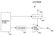
そこで、高効率に動作する送信回路として、ポーラ変調方式が適用された送信回路が従来から提案されている。図26は、ポーラ変調方式が適用された従来の送信回路500の構成を示すブロック図である。図26において、従来の送信回路500は、極座標信号生成部501、角度変調部502、電源端子503、レギュレータ504、振幅変調部505、及び出力端子506を備える。
Therefore, a transmission circuit to which a polar modulation method is applied has been proposed as a transmission circuit that operates with high efficiency. FIG. 26 is a block diagram showing a configuration of a conventional transmission circuit 500 to which the polar modulation method is applied. In FIG. 26, the conventional transmission circuit 500 includes a polar coordinate
極座標信号生成部501は、振幅信号及び位相信号を生成する。振幅信号は、レギュレータ504に入力される。レギュレータ504には、電源端子503から直流電圧が供給されている。レギュレータ504は、入力された振幅信号に応じた電圧を振幅変調部505に供給する。また、位相信号は、角度変調部502に入力される。角度変調部502は、入力された位相信号を角度変調して角度変調信号を出力する。角度変調部502から出力された角度変調信号は、振幅変調部505に入力される。振幅変調部505は、角度変調信号をレギュレータ504から供給された電圧で振幅変調して、変調信号として出力する。この変調信号が、送信信号として出力端子506から出力される。
The polar coordinate
また、ポーラ変調方式が適用された送信回路には、レギュレータ504や振幅変調部505の非線形性によって、送信信号に歪みが生じることがある。ポーラ変調方式が適用された送信回路において、レギュレータ504や振幅変調部505の非線形性を、テーブルを用いて補償する手法が従来から開示されている(例えば、特許文献1参照)。このような手法を用いた従来の送信回路としては、例えば、図27に示す送信回路600がある。図27は、従来の送信回路600の構成の一例を示すブロック図である。図27において、歪み補償部601は、送信信号に基づいて、レギュレータ504や振幅変調部505の非線形性を補償するように、歪み補償テーブルを作成する。振幅制御部602、及び位相制御部603は、歪み補償部601が作成した歪み補償テーブルに基づいて、振幅信号及び位相信号を予め歪ませて、レギュレータ504及び振幅変調部505に入力する。
しかしながら、近年、送信回路に求められる変調帯域が広帯域化しており、これによって、レギュレータ504や振幅変調部505の周波数帯域が不足することが予想される。例えば、従来の送信回路500(図26参照)においては、レギュレータ504や振幅変調部505の周波数帯域が不十分な場合、送信信号が歪むなどの問題が発生していた。一例として、送信回路500において、レギュレータ504及び振幅変調部505の周波数帯域が不十分な場合のシミュレーション結果を図28に示す。ただし、変調信号には、シンボル数512、オーバーサンプリング128倍、ルートレイズドフィルタα=0.5、シンボルレート3.84MHzのπ/4シフトQPSKの変調波を用いるものとする。また、レギュレータ504と振幅変調部505とを合わせた伝達特性を、カットオフ周波数が26.4MHzの1次の減衰特性を有する低域通過フィルタと同じにする。
However, in recent years, the modulation band required for the transmission circuit is widened, and it is expected that the frequency band of the
このときの隣接チャネル漏洩電力(ACP)について、積分帯域幅を3.84MHzとし、5MHz離調、及び10MHz離調のときの値を計算し、この結果を図28に示している。図28において、横軸(すなわち、Delay)は、位相信号と比べた振幅信号の遅延時間であり、単位はサンプル数である。例えば、1サンプルの遅延は、2nsに相当する。また、−5MHzのACPとは、中心周波数より5MHz周波数が小さい点のACPを表す。この結果から、経路の違いによる振幅信号と位相信号との遅延時間を調整しても、ACPが十分小さくならず、また、離調が異なるACPで最適遅延時間が異なるため、すべてのACPを小さくすることが困難であることが分かる。 With respect to the adjacent channel leakage power (ACP) at this time, the integration bandwidth was set to 3.84 MHz, and values at 5 MHz detuning and 10 MHz detuning were calculated. The results are shown in FIG. In FIG. 28, the horizontal axis (that is, Delay) is the delay time of the amplitude signal compared to the phase signal, and the unit is the number of samples. For example, a delay of 1 sample corresponds to 2 ns. The -5 MHz ACP represents an ACP at a point where the 5 MHz frequency is smaller than the center frequency. From this result, even if the delay time between the amplitude signal and the phase signal due to the path difference is adjusted, the ACP is not sufficiently small, and the optimum delay time is different in the ACP having different detuning. It turns out that it is difficult to do.
また、送信回路600(図27参照)は、レギュレータ504や振幅変調部505の非線形性を補償しても、レギュレータ504や振幅変調部505の周波数帯域が不十分なことによって発生する歪みを抑制することは困難である。
In addition, the transmission circuit 600 (see FIG. 27) suppresses distortion caused by insufficient frequency bands of the
それ故に、本発明の目的は、変調帯域が広い変調方式においても、低歪みかつ高効率に動作する送信回路、及びそれを用いた通信機器を提供することである。 Therefore, an object of the present invention is to provide a transmission circuit that operates with low distortion and high efficiency even in a modulation scheme with a wide modulation band, and a communication device using the transmission circuit.
本発明の目的は、入力されるデータに基づいて、送信信号を生成して出力する送信回路に向けられている。そして、上記目的を達成させるために、本発明の送信回路は、データを信号処理することによって得られる振幅成分および位相成分に基づいて、振幅信号および角度変調信号を生成する信号生成部と、所定の特性に基づいて、振幅信号に対して波形整形処理を行う補償フィルタと、補償フィルタで波形整形処理された信号の大きさに応じた信号を出力するレギュレータと、角度変調信号をレギュレータから出力された信号で振幅変調して、変調信号として出力する振幅変調部とを備える。ただし、補償フィルタの特性は、レギュレータの入力と振幅変調部の出力との間の伝達特性に対して、逆特性である。 An object of the present invention is directed to a transmission circuit that generates and outputs a transmission signal based on input data. In order to achieve the above object, the transmission circuit of the present invention includes a signal generation unit that generates an amplitude signal and an angle modulation signal based on an amplitude component and a phase component obtained by signal processing of data, A compensation filter that performs waveform shaping on the amplitude signal, a regulator that outputs a signal according to the magnitude of the waveform shaped signal by the compensation filter, and an angle modulation signal from the regulator. And an amplitude modulation unit that performs amplitude modulation with the obtained signal and outputs the modulated signal. However, the characteristics of the compensation filter are opposite to the transfer characteristics between the input of the regulator and the output of the amplitude modulator.
好ましくは、信号生成部は、データを信号処理することによって得られる振幅成分および位相成分に基づいて、振幅信号および位相信号を生成する極座標信号生成部と、位相信号を角度変調して、角度変調信号として出力する角度変調部とを含む。 Preferably, the signal generation unit includes a polar signal generation unit that generates an amplitude signal and a phase signal based on an amplitude component and a phase component obtained by performing signal processing on the data, and angle-modulates the phase signal to perform angle modulation. And an angle modulation unit that outputs the signal.
また、信号生成部は、データを信号処理することによって、直交データであるI,Q信号からなるベースバンド信号を生成する直交信号生成部と、I,Q信号をベクトル変調するベクトル変調部と、ベクトル変調部から出力された信号の包絡線成分を検波して、当該検波した包絡線成分を振幅信号として出力する包絡線検波部と、ベクトル変調部から出力された信号の包絡線を所定の大きさに制限して、大きさが制限された信号を角度変調信号として出力するリミッタとを含んでいてもよい。 The signal generation unit performs signal processing on the data to generate a baseband signal including I and Q signals that are orthogonal data, a vector modulation unit that vector-modulates the I and Q signals, An envelope detector for detecting the envelope component of the signal output from the vector modulator and outputting the detected envelope component as an amplitude signal; and an envelope of the signal output from the vector modulator for a predetermined size In addition, a limiter that outputs a signal whose size is limited as an angle modulation signal may be included.
好ましくは、補償フィルタは、所定の特性に基づいて、振幅信号に対して波形整形処理を行うデジタルフィルタと、デジタルフィルタから出力された信号をアナログ信号に変換するDAコンバータとを含む。 Preferably, the compensation filter includes a digital filter that performs waveform shaping processing on the amplitude signal based on predetermined characteristics, and a DA converter that converts a signal output from the digital filter into an analog signal.
また、補償フィルタは、振幅信号をアナログ信号に変換するDAコンバータと、所定の特性に基づいて、アナログ信号に対して波形整形処理を行なうアナログフィルタとを含むものであってもよい。 The compensation filter may include a DA converter that converts an amplitude signal into an analog signal, and an analog filter that performs waveform shaping processing on the analog signal based on predetermined characteristics.
好ましくは、レギュレータは、シリーズレギュレータである。これによって、送信回路は、広帯域な信号を処理することができる。 Preferably, the regulator is a series regulator. Thereby, the transmission circuit can process a broadband signal.
また、レギュレータは、スイッチングレギュレータであってもよい。これによって、送信回路は、高効率な動作が可能となる。 The regulator may be a switching regulator. As a result, the transmission circuit can operate with high efficiency.
また、送信回路は、極座標信号生成部の出力に、振幅信号、および位相信号のうち少なくともいずれかの信号を、レギュレータ、角度変調部及び振幅変調部の少なくともいずれかで発生する歪みが抑制されるように補償する歪み補償部をさらに備えてもよい。 In addition, the transmission circuit suppresses distortion generated by at least one of the amplitude signal and the phase signal in at least one of the regulator, the angle modulation unit, and the amplitude modulation unit at the output of the polar coordinate signal generation unit. A distortion compensation unit that compensates for this may be further included.
好ましくは、信号生成部は、ベースバンドに基づいて設定される電力情報をさらに出力する。この場合、レギュレータは、スイッチングレギュレータとシリーズレギュレータとを含む。スイッチングレギュレータは、電力情報によって制御された電圧をシリーズレギュレータに供給する。シリーズレギュレータは、スイッチングレギュレータから供給された電圧で、補償フィルタで波形整形処理された信号の大きさに応じた信号を出力する。これによって、送信回路は、シリーズレギュレータでの損失を小さくし、消費電力を低減することができる。 Preferably, the signal generation unit further outputs power information set based on the baseband. In this case, the regulator includes a switching regulator and a series regulator. The switching regulator supplies a voltage controlled by the power information to the series regulator. The series regulator outputs a signal corresponding to the magnitude of the signal subjected to waveform shaping by the compensation filter, using the voltage supplied from the switching regulator. As a result, the transmission circuit can reduce loss in the series regulator and reduce power consumption.
好ましくは、補償フィルタの伝達特性は、振幅信号の大きさによらず一定である。ただし、信号生成部が、ベースバンドに基づいて設定される電力情報をさらに出力する場合には、補償フィルタの伝達特性を、電力情報の大きさによって変化させてもよい。これによって、送信回路は、振幅変調部が出力する送信信号の電力の大きさに関わらず、レギュレータ及び振幅変調部の周波数帯域が不十分なことによって発生する歪みを抑制することができる。 Preferably, the transfer characteristic of the compensation filter is constant regardless of the magnitude of the amplitude signal. However, when the signal generator further outputs power information set based on the baseband, the transfer characteristic of the compensation filter may be changed depending on the magnitude of the power information. As a result, the transmission circuit can suppress distortion caused by insufficient frequency bands of the regulator and the amplitude modulation unit regardless of the magnitude of the power of the transmission signal output from the amplitude modulation unit.
また、本発明は、上述した送信回路を備える通信機器にも向けられている。通信機器は、送信信号を生成する送信回路と、送信回路で生成された送信信号を出力するアンテナとを備える。また、通信機器は、アンテナから受信した受信信号を処理する受信回路と、送信回路で生成された送信信号をアンテナに出力し、アンテナから受信した受信信号を受信回路に出力するアンテナ共用部とをさらに備えてもよい。 The present invention is also directed to a communication device including the above-described transmission circuit. The communication device includes a transmission circuit that generates a transmission signal and an antenna that outputs the transmission signal generated by the transmission circuit. In addition, the communication device includes a reception circuit that processes a reception signal received from the antenna, and an antenna sharing unit that outputs the transmission signal generated by the transmission circuit to the antenna and outputs the reception signal received from the antenna to the reception circuit. Further, it may be provided.
以上のように、本発明によれば、補償フィルタが、信号生成部が出力する振幅信号を、レギュレータの入力から振幅変調部の出力までの伝達特性と逆特性になるように補償することで、レギュレータ及び振幅変調部の周波数帯域が不十分なことによって発生する歪みを抑制する。これによって、送信回路は、変調帯域が広い変調方式においても、低歪みかつ高効率に送信信号を出力することができる。 As described above, according to the present invention, the compensation filter compensates the amplitude signal output from the signal generation unit so as to be opposite to the transfer characteristic from the input of the regulator to the output of the amplitude modulation unit, Suppresses distortion caused by insufficient frequency bands of the regulator and the amplitude modulator. As a result, the transmission circuit can output a transmission signal with low distortion and high efficiency even in a modulation scheme with a wide modulation band.
また、送信回路は、角度変調部、レギュレータ、及び振幅変調部の少なくともいずれかの非線形を補償する歪み補償部をさらに備える。これによって、送信回路は、歪み補償部が、角度変調部、レギュレータ、及び振幅変調部の少なくともいずれかの非線形を補償し、補償フィルタが、レギュレータ及び振幅変調部の周波数帯域が不十分なことによって発生する歪みを抑制するので、より低歪みな送信信号を出力することができる。 The transmission circuit further includes a distortion compensator that compensates for at least one of the angle modulator, the regulator, and the amplitude modulator. Thereby, in the transmission circuit, the distortion compensator compensates at least one of the nonlinearity of the angle modulator, the regulator, and the amplitude modulator, and the compensation filter has an insufficient frequency band of the regulator and the amplitude modulator. Since the generated distortion is suppressed, a transmission signal with lower distortion can be output.
また、本発明の通信機器によれば、上述した送信回路を用いることで、広い帯域幅で出力信号の精度を確保しつつ、小型かつ高効率に動作することができる。 Further, according to the communication device of the present invention, by using the transmission circuit described above, it is possible to operate in a small size and with high efficiency while ensuring the accuracy of the output signal with a wide bandwidth.
(第1の実施形態)
図1は、本発明の第1の実施形態に係る送信回路1の構成の一例を示すブロック図である。図1において、送信回路1は、信号生成部11、補償フィルタ12、電源端子13、レギュレータ14、振幅変調部15、及び出力端子16を備える。信号生成部11は、入力データを信号処理することによって得られる振幅成分及び位相成分に基づいて、振幅信号M及び角度変調信号Sθを出力する。振幅信号Mは、補償フィルタ12で波形整形処理された後、レギュレータ14に入力される。レギュレータ14は、入力された振幅信号によって制御された信号を出力する。典型的には、レギュレータ14は、入力された振幅信号の大きさに比例した信号を出力する。レギュレータ14が出力した信号は、振幅変調部15に入力される。
(First embodiment)
FIG. 1 is a block diagram showing an example of the configuration of the
角度変調信号Sθは、振幅変調部15に入力される。振幅変調部15は、角度変調信号Sθをレギュレータ14から入力された信号で振幅変調して、角度変調及び振幅変調された変調信号として出力する。変調信号は、出力端子16から送信信号として出力される。
The angle modulation signal Sθ is input to the
次に、信号生成部11、レギュレータ14、振幅変調部15、及び補償フィルタ12の順に、各構成の詳細について説明する。
Next, details of each component will be described in the order of the
信号生成部11は、例えば、極座標信号を生成する極座標信号生成部を用いて構成することができる。図2は、極座標信号生成部を用いて構成した信号生成部11aの一例を示すブロック図である。図2において、信号生成部11aは、極座標信号生成部111、角度変調部112、出力端子113、及び出力端子114を含む。極座標信号生成部111は、入力データを変調して、振幅信号Mと位相信号θとを生成する。振幅信号Mは、出力端子113から出力される。位相信号θは、角度変調部112で角度変調された後、角度変調信号Sθとして、出力端子114から出力される。
The
また、信号生成部11は、例えば、直交信号を生成する直交信号生成部を用いて構成してもよい。図3は、直交信号生成部を用いて構成した信号生成部11bの一例を示すブロック図である。図3において、信号生成部11bは、直交信号生成部115、ベクトル変調部116、包絡線検波部117、リミッタ118、出力端子113、及び出力端子114を含む。直交信号生成部115は、直交データであるI,Q信号からなるベースバンド信号を生成する。I,Q信号は、ベクトル変調部116に入力される。ベクトル変調部116は、I,Q信号をベクトル変調する。ベクトル変調部116には、例えば、直交変調器が用いられる。
Moreover, you may comprise the
ベクトル変調部116から出力された信号は、包絡線検波部117及びリミッタ118に入力される。包絡線検波部117は、ベクトル変調部116から出力された信号の包絡線成分を検波し、検波した包絡線成分を振幅信号Mとして、出力端子113から出力する。リミッタ118は、ベクトル変調部116から出力された信号の包絡線成分を一定の大きさに制限し、大きさを制限した信号を角度変調信号Sθとして、出力端子114から出力する。
The signal output from the
レギュレータ14は、例えば、電圧駆動型のシリーズレギュレータで構成することができる。図4は、シリーズレギュレータ14aの構成の一例を示すブロック図である。図4において、シリーズレギュレータ14aは、入力端子141、比較部142、電源端子143、トランジスタ144、及び出力端子145を含む。ここでは、トランジスタ144を電界効果トランジスタとする。入力端子141には、補償フィルタ12を介して振幅信号が入力される。振幅信号は、比較部142を介してトランジスタ144のゲート端子に入力される。トランジスタ144のドレイン端子には、電源端子143から直流電圧が供給されている。
The
トランジスタ144は、入力された振幅信号の大きさに比例した電圧をソース端子から出力する。トランジスタ144のソース端子から出力された電圧は、比較部142にフィードバックされる。比較部142は、フィードバックされた電圧に基づいて、トランジスタ144のゲート端子に入力される振幅信号の大きさを調整する。このようにして、シリーズレギュレータ14aは、振幅信号の大きさに応じて制御された電圧を出力端子145から安定して供給することができる。なお、トランジスタ144は、バイポーラトランジスタであっても同様の効果が得られる。
The
また、レギュレータ14は、例えば、電圧駆動型のスイッチングレギュレータで構成することができる。図5は、スイッチングレギュレータ14bの構成の一例を示すブロック図である。図5において、スイッチングレギュレータ14bは、入力端子141、電源端子143、信号変換部146、増幅部147、ローパスフィルタ148及び出力端子145を含む。入力端子141には、補償フィルタ12を介して振幅信号が入力される。振幅信号は、信号変換部146に入力される。信号変換部146は、入力された振幅信号をPWMやデルタシグマ変調された信号に変換する。信号変換部146で変換された信号は、増幅部147に入力される。増幅部147は、入力された信号を増幅して出力する。なお、増幅部147には、電源端子143から直流電圧が供給されている。増幅部147には、D級アンプなどの高効率スイッチングアンプが用いられる。
Moreover, the
増幅部147が出力した信号は、ローパスフィルタ148に入力される。ローパスフィルタ148は、増幅部147が出力した信号から量子化雑音やスイッチング雑音などのスプリアス成分を除去する。ローパスフィルタ148でスプリアス成分が除去された信号は、振幅信号の大きさに応じて制御された電圧として、出力端子145から出力される。なお、スイッチングレギュレータ14bは、出力する電圧を安定化させるために、ローパスフィルタ148から出力される信号を、信号変換部146にフィードバックしてもよい。送信回路1は、レギュレータ14に高効率なスイッチングレギュレータ14bを用いることで、送信回路としての消費電力を低減することができる。
The signal output from the amplifying
また、レギュレータ14は、例えば、電流駆動型のレギュレータで構成することができる。図6は、電流駆動型のレギュレータ14cの構成の一例を示すブロック図である。図6において、電流駆動型のレギュレータ14cは、入力端子141、電源端子143、可変電流源149、トランジスタ144x、トランジスタ144y、及び出力端子145を含む。入力端子141には、補償フィルタ12を介して振幅信号が入力される。電源端子143には、直流電圧が供給されている。入力された振幅信号は、可変電流源149、トランジスタ144x、及びトランジスタ144yを介して、振幅信号の大きさに応じて制御された電流として、出力端子145から出力される。このような電流駆動型のレギュレータ14cは、振幅変調部15がバイポーラトランジスタで構成されているときに有用である。なお、トランジスタ144x、及びトランジスタ144yは、電界効果トランジスタであっても、バイポーラトランジスタであっても同様の効果が得られる。
Moreover, the
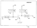
振幅変調部15は、例えば、図7に示すように構成することができる。図7は、振幅変調部15aの構成の一例を示すブロック図である。図7において、振幅変調部15aは、入力端子151、整合回路152、バイアス回路153、電源端子154、トランジスタ155、バイアス回路156、入力端子157、整合回路158、及び出力端子159を含む。ここでは、トランジスタ155をバイポーラトランジスタとする。入力端子151には、信号生成部11から角度変調信号Sθが入力される。角度変調信号Sθは、整合回路152を介して、トランジスタ155のベース端子に入力される。
The
また、電源端子154には、直流電圧が印加されている。すなわち、トランジスタ155のベース端子には、電源端子154、及びバイアス回路153を介して、バイアス電圧が供給される。入力端子157には、レギュレータ17から振幅信号の大きさに応じて制御された信号が入力される。振幅信号の大きさに応じて制御された信号は、バイアス回路156を介して、トランジスタ155のコレクタ端子に入力される。トランジスタ155は、角度変調信号Sθを振幅信号の大きさに応じて制御された信号によって振幅変調して、角度変調及び振幅変調された変調信号として出力する。
Further, a DC voltage is applied to the
トランジスタ155から出力された変調信号は、整合回路158を介して、出力端子159から出力される。なお、トランジスタ155は、電界効果トランジスタであっても同様の効果が得られる。また、振幅変調部15aは、電源端子154と、入力端子157とに入力される信号を入替えてもよく、この場合も、同様の効果を得ることができる。
The modulation signal output from the
なお、振幅変調部15は、上述した振幅変調部15aとは異なる構成であってもよい。図8は、振幅変調部15bの構成の一例を示すブロック図である。図8において、振幅変調部15bは、基本的には、振幅変調部15a(図7参照)を直列に2つ接続した構成である。トランジスタ155のベース端子には、バイアス回路153を介して、電源端子154からバイアス電圧が供給される。トランジスタ161のベース端子には、バイアス回路165を介して、電源端子160からバイアス電圧が供給される。
The
トランジスタ155のコレクタ端子には、端子164、及びバイアス回路156を介して、レギュレータ17から振幅信号の大きさに応じて制御された信号が入力される。また、トランジスタ161のコレクタ端子には、端子164、及びバイアス回路162を介して、レギュレータ17から振幅信号の大きさに応じて制御された信号が入力される。この構成によって、振幅変調部15bは、図7に示した振幅変調部15aと比較して、より大きなダイナミックレンジを持った信号を出力することができる。なお、振幅変調部15a、15bにおいて、トランジスタをバイポーラトランジスタとしたが、電界効果トランジスタとしても同様の効果が得られる。
A signal controlled according to the magnitude of the amplitude signal is input from the
次に、補償フィルタ12の詳細について説明する。補償フィルタ12は、振幅信号Mを波形整形処理することで、レギュレータ14及び振幅変調部15の周波数帯域が不十分なことによって発生する歪み(以下、このような歪みを周波数特性と記す)を補償する。ここで、補償フィルタ12の設計方法について説明する。
Next, details of the
補償フィルタ12を設計するには、まず、レギュレータ14の入力から振幅変調部15の出力までの間の伝達特性H(s)を求める必要がある。この伝達特性H(s)は、レギュレータ14への入力信号X(s)と、振幅変調部15からの出力信号の包絡線成分Y(s)とを用いて、式(1)によって定義される。
H(s)=Y(s)/X(s) ・・・式(1)
In order to design the
H (s) = Y (s) / X (s) (1)
図9は、レギュレータ14の入力から振幅変調部15の出力までの間の伝達特性H(s)を求める方法を説明する図である。図9において、信号源171、172から正弦波信号が出力される。ここで、信号源171が出力する正弦波信号の周波数は、信号生成部11(図1参照)が出力する角度変調信号Sθの中心周波数と等しく設定される。また、信号源172が出力する正弦波信号の周波数は、信号生成部11(図1参照)が出力する振幅信号Mが有する周波数のいずれかを含むように設定される。なお、信号源172から出力される信号としては、ステップ信号などを用いてもよい。
FIG. 9 is a diagram for explaining a method for obtaining the transfer characteristic H (s) from the input of the
信号源171から出力された正弦波信号は、振幅変調部15に入力される。一方、信号源172から出力された正弦波信号は、レギュレータ14で増幅された後、振幅変調部15に入力される。振幅変調部15は、信号源171から出力された正弦波信号を、レギュレータ14を介して入力された正弦波信号で振幅変調して、変調信号として出力する。包絡線検波部173は、振幅変調部15から出力された変調信号の包絡線成分を検波し、検波した包絡線成分を包絡線信号Y(s)として、オシロスコープ174に出力する。なお、包絡線検波部173には、伝達特性が既知のものが用いられる。
The sine wave signal output from the
また、オシロスコープ174には、レギュレータへの入力信号X(s)として、信号源172から正弦波信号が入力される。すなわち、オシロスコープ174によって、包絡線信号Y(s)を測定し、レギュレータへの入力信号X(s)の周波数をスイープすることによって、レギュレータ14の入力から包絡線検波部173の出力までの伝達特性H1(s)を求めることができる。ここで、包絡線検波部173の伝達特性をH2(s)とすると、レギュレータ14の入力から振幅変調部15の出力までの伝達特性H(s)は、式(2)で表すことができる。
H(s)=H1(s)/H2(s) ・・・式(2)
The
H (s) = H1 (s) / H2 (s) (2)
ここで、伝達特性H(s)が、1次の伝達特性を有する場合、補償フィルタ12は、式(3)を満たすように設計される。ただし、ω0はカットオフ周波数を表す定数であり、s=jωである。
H(s)=1/(1+s/ω0) ・・・式(3)
Here, when the transfer characteristic H (s) has a first-order transfer characteristic, the
H (s) = 1 / (1 + s / ω 0 ) (3)
補償フィルタ12は、例えば、デジタルフィルタを用いて構成することができる。図10は、デジタルフィルタを用いて構成された補償フィルタ12aの一例を示すブロック図である。図10において、補償フィルタ12aは、入力端子121、デジタルフィルタ122、DAコンバータ123、及び出力端子124を含む。補償フィルタ12aは、入力端子121を介して入力された振幅信号Mを、デジタルフィルタ122で補償し、DAコンバータ123でアナログ信号に変換して、出力端子124から出力する。
The
式(3)をデジタル形式で表現する(すなわち、zの関数として表現する)と、式(4)で表すことができる。ここで、Tはクロック周波数の逆数である。
H(z)=(1−exp(−ω0T))/(1−exp(−ω0T)・z-1) ・・・式(4)
When Expression (3) is expressed in digital form (that is, expressed as a function of z), it can be expressed by Expression (4). Here, T is the reciprocal of the clock frequency.
H (z) = (1−exp (−ω 0 T)) / (1−exp (−ω 0 T) · z −1 ) (4)
補償フィルタ12aの伝達特性Hc(z)は、レギュレータ14の入力から振幅変調部15の出力までの伝達特性H(z)と逆特性となるので、式(5)で表すことができる。第1の実施形態に係る補償フィルタ12aの伝達特性Hc(z)は、式(5)に示すように、振幅信号Mの大きさによらず一定である。
Hc(z)=H(z)-1
=(1−exp(−ω0T)・z―1)/(1−exp(−ω0T)) ・・・式(5)
Since the transfer characteristic Hc (z) of the compensation filter 12a is opposite to the transfer characteristic H (z) from the input of the
Hc (z) = H (z) −1
= (1-exp (-ω 0 T) · z− 1 ) / (1-exp (−ω 0 T)) (5)
また、この補償フィルタ12aは、図11に示すFIRフィルタによって表すことができる。図11は、FIRフィルタの構成の一例を示すブロック図である。図11に示すFIRフィルタは、入力端子1221、遅延素子1222、乗数器(掛算器)1223、1224、加算器1225、及び出力端子1226から構成される。図11において、乗数器1223、1224の係数b0、b1は、式(6)及び式(7)で表すことができる。
b0=1−exp(−ω0T)・z-1 ・・・式(6)
b1=exp(−ω0T)/(1−exp(−ω0T)) ・・・式(7)
The compensation filter 12a can be represented by an FIR filter shown in FIG. FIG. 11 is a block diagram illustrating an example of the configuration of the FIR filter. The FIR filter shown in FIG. 11 includes an
b 0 = 1−exp (−ω 0 T) · z −1 (6)
b 1 = exp (−ω 0 T) / (1-exp (−ω 0 T)) (7)
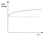
図12は、送信回路1において、図28と同様の条件で、FIRフィルタのクロック周波数を変化させたときのシミュレーション結果を示す図である。ただし、図12では、振幅信号と位相信号との間の遅延時間は最適に調整されている(すなわち、Delay=0である)ものとする。図12に示すように、送信回路1は、低いクロック周波数においても、補償フィルタ12を用いることで、歪みを大きく低減できることがわかる。
FIG. 12 is a diagram illustrating a simulation result when the clock frequency of the FIR filter is changed in the
また、補償フィルタ12は、例えば、アナログ回路を用いて構成してもよい。この場合も、補償フィルタ12は、レギュレータ14の入力から振幅変調部15の出力までの伝達特性H(s)と逆特性になるように設計される。図13は、アナログ回路を用いて構成された補償フィルタ12bの一例を示すブロック図である。図13において、補償フィルタ12bは、入力端子121、DAコンバータ125、アナログフィルタ126、及び出力端子124を含む。補償フィルタ12bは、入力端子121を介して入力された振幅信号Mを、DAコンバータ125でアナログ信号に変換した後、アナログフィルタ126で補償し、出力端子124から出力する。
The
以上のように、本発明の第1の実施形態に係る送信回路1によれば、補償フィルタ12が、信号生成部11が出力する振幅信号を、レギュレータ14の入力から振幅変調部15の出力までの伝達特性と逆特性になるように補償することで、レギュレータ504及び振幅変調部505の周波数帯域が不十分なことによって発生する歪みを抑制する。これによって、送信回路は、変調帯域が広い変調方式においても、低歪みかつ高効率に動作することができる。
As described above, according to the
また、スイッチングレギュレータとシリーズレギュレータとを比較すると、一般的に、スイッチングレギュレータには、高効率であるという利点があるが、帯域が狭いという欠点がある。しかしながら、送信回路1は、補償フィルタ12を用いることで、帯域が狭くても低歪みに動作することから、従来はシリーズレギュレータでなければ変調帯域が確保できなかった場合も、高効率なスイッチングレギュレータを適用することができる。これによって、送信回路1は、低消費電力をより低減することができる。
In addition, when switching regulators are compared with series regulators, switching regulators generally have the advantage of high efficiency, but have the disadvantage of narrow bandwidth. However, since the
(第2の実施形態)
図14Aは、本発明の第2の実施形態に係る送信回路2の構成の一例を示すブロック図である。図14Aにおいて、送信回路2は、信号生成部11cの構成が第1の実施形態と異なる。信号生成部11cは、極座標信号生成部111、歪み補償部119、及び角度変調部112を含む。図14Aにおいて、歪み補償部119は、極座標信号生成部111で生成された振幅信号M1及び位相信号θ1を、レギュレータ14、角度変調部112及び振幅変調部15の少なくともいずれかで発生する歪みが抑制されるように補償する。
(Second Embodiment)
FIG. 14A is a block diagram showing an example of the configuration of the
具体的には、歪み補償部119は、補償フィルタ12中のDACへの入力信号に対する振幅変調部15から出力される送信信号の包絡線の大きさ(AM/AM特性)、および補償フィルタ12中のDACへの入力信号に対する振幅変調部15の入出力間の位相差(AM/PM特性)と逆特性となるように、歪み補償テーブルを元に、予め入力された信号を歪ませる。
Specifically, the distortion compensator 119 includes the magnitude of the envelope of the transmission signal (AM / AM characteristics) output from the
図14Aにおいて、極座標信号生成部111は、振幅信号M1及び位相信号θ1を出力する。振幅信号M1及び位相信号θ1は、歪み補償部119に入力される。歪み補償部119は、予め作成しておいた歪み補償テーブルに基づいて、振幅信号M1及び位相信号θ1を補償し、振幅信号M2及び位相信号θ2を出力する。以降の動作は、第1の実施形態と同様である。すなわち、振幅信号M2は、補償フィルタ12に入力され、波形整形処理された後、レギュレータ14に入力される。位相信号θ2は、角度変調部112に入力され、角度変調された後、振幅変調部15に入力される。
In FIG. 14A, the polar coordinate
以下に、歪み補償部119における歪み補償テーブルの作成方法について説明する。歪み補償テーブルは、送信回路2の設計時に作成される。まず、歪み補償部119は、角度変調部112に一定の位相θ2(例えば、θ2=0)を入力する。また、歪み補償部119は、補償フィルタ12に一定の大きさの振幅信号M2を入力する。歪み補償部119は、このときの振幅変調部15から出力される変調信号の包絡線の大きさ(以下、振幅信号M3とする)、及び変調信号の位相成分(以下、位相信号θ3とする)を測定する。歪み補償部119は、補償フィルタ12に入力する振幅信号M2の大きさを変えてこれを繰り返す。このときの特性が図15A、及び図15Bのようになったとする。
A method for creating a distortion compensation table in the distortion compensation unit 119 will be described below. The distortion compensation table is created when the
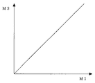
このような場合、歪み補償部119は、図15A及び図15Bで示した特性と逆特性となるように(すなわち、図16A及び図16Bで示す特性となるように)、振幅信号M1及び位相信号θ1を歪ませる歪み補償テーブルを作成する。これによって、歪み補償部119は、送信回路2の特性を、図17A及び図17Bに示すような線形特性にすることができる。
In such a case, the distortion compensator 119 has the amplitude signal M1 and the phase signal so as to have characteristics opposite to those shown in FIGS. 15A and 15B (that is, characteristics shown in FIGS. 16A and 16B). A distortion compensation table for distorting θ1 is created. As a result, the distortion compensator 119 can make the characteristics of the
なお、第2の実施形態に係る送信回路2は、図14Aとは異なる構成であってもよい。例えば、第2の実施形態に係る送信回路2は、図14Bに示すように構成することができる。図14Bにおいて、送信回路2bは、信号生成部11の後段に、歪み補償部119を備える。
Note that the
以上のように、本発明の第2の実施形態に係る送信回路2によれば、歪み補償部119が、角度変調部112、レギュレータ14、及び振幅変調部15の少なくともいずれかの非線形を補償し、補償フィルタ12が、レギュレータ14及び振幅変調部15の周波数帯域が不十分なことによって発生する歪みを抑圧するので、より低歪みな送信信号を出力することができる。
As described above, according to the
(第3の実施形態)
図18は、本発明の第3の実施形態に係る送信回路3の構成の一例を示すブロック図である。図18において、送信回路3は、第1の実施形態に係る送信回路1と比較して、信号生成部1cと、レギュレータ14dとが異なる。信号生成部11cは、第1の実施形態に係る信号生成部1と比較して、さらにベースバンドに基づいて設定される電力情報Pを出力する。レギュレータ14dは、シリーズレギュレータ14a、及びスイッチングレギュレータ14bを含む。シリーズレギュレータ14aは、例えば、図4に示す構成である。スイッチングレギュレータ14bは、例えば、図5に示す構成である。
(Third embodiment)
FIG. 18 is a block diagram showing an example of the configuration of the
電力情報Pは、例えば、W−CDMAシステムの場合、基地局によって制御される。すなわち、送信すべき電力が基地局から送信回路3に送られる。送信回路3は、この基地局から送られた電力に基づいて、電力情報Pを決定する。電力情報Pは、スイッチングレギュレータ14bに入力される。スイッチングレギュレータ14bには、電源端子13から直流電圧が供給されている。スイッチングレギュレータ14bは、電力情報Pによって制御された電圧をシリーズレギュレータ14aに供給する。電力情報Pは、振幅信号Mと比べて周波数が低いため、スイッチングレギュレータ14bを高効率に動作させることができる。なお、スイッチングレギュレータ14bから出力される電圧は、シリーズレギュレータ14aから出力される電圧の最大値と同等か、少し高い電圧となるように設定される。
For example, in the case of a W-CDMA system, the power information P is controlled by a base station. That is, power to be transmitted is transmitted from the base station to the
シリーズレギュレータ14aは、スイッチングレギュレータ14bから供給される電圧が最適に制御されているため、高効率に動作することができる。このため、送信回路3は、シリーズレギュレータ14aとスイッチングレギュレータ14bとを組み合わせたレギュレータ14dを用いることで、シリーズレギュレータ14aでの損失を小さくし、消費電力を低減することができる。また、送信回路3は、補償フィルタ12が、シリーズレギュレータ14a及び振幅変調部15の周波数特性を補償するので、送信信号の線形性を高めることができる。
The
なお、送信回路3は、上述した歪み補償部17をさらに備えてもよい。図19は、歪み補償部17を備える送信回路3bの構成の一例を示すブロック図である。図19において、送信回路3bは、歪み補償部17が、シリーズレギュレータ14a、及び振幅変調部15の少なくともいずれかの非線形性を補償するので、さらに、送信信号の線形性を高めることができる。
The
(第4の実施形態)
図20は、本発明の第4の実施形態に係る送信回路4の構成の一例を示すブロック図である。図20において、送信回路4は、信号生成部11c、補償フィルタ12c、電源端子13、レギュレータ14、振幅変調部15、及び出力端子16を備える。補償フィルタ12cには、信号生成部11cから出力された電力情報Pが入力される。振幅変調部15が出力する送信信号の電力の大きさによっては、レギュレータ14から振幅変調部15までの伝達特性は変化する場合がある。このため、送信回路4は、信号生成部11cから出力された電力情報Pの大きさに応じて、補償フィルタ12cの特性を最適に制御する。
(Fourth embodiment)
FIG. 20 is a block diagram showing an example of the configuration of the
図21は、補償フィルタ12cの詳細な構成の一例を示すブロック図である。図21において、補償フィルタ12cは、入力端子121、デジタルフィルタ122、DAコンバータ123、制御部127、及び出力端子128を含む。入力端子121には、振幅信号Mが入力される。補償フィルタ12cは、入力端子121を介して入力された振幅信号Mを、デジタルフィルタ122で補償し、DAコンバータ123でアナログ信号に変換して、出力端子124から出力する。また、入力端子128には、電力情報Pが入力される。制御部127には、電力情報Pとデジタルフィルタ122のタップ係数とを対応付けたテーブルが格納されている。制御部127は、入力された電力情報Pとこのテーブルとに基づいて、デジタルフィルタ122のタップ係数を制御する。これによって、送信回路4は、振幅変調部15が出力する送信信号の電力の大きさに関わらず、レギュレータ14及び振幅変調部15の周波数帯域が不十分なことによって発生する歪みを抑制することができる。
FIG. 21 is a block diagram illustrating an example of a detailed configuration of the
なお、送信回路4は、補償フィルタ12cを可変容量コンデンサを有するアナログフィルタで構成してもよい。この場合、制御部127には、電力情報Pと可変容量コンデンサの容量とを対応付けたテーブルが格納される。制御部127は、入力された電力情報Pとこのテーブルとに基づいて、デジタルフィルタ122の可変容量コンデンサの容量を制御する。
In the
また、送信回路4は、電力情報Pの代わりに、振幅変調部15が出力する送信信号の包絡線の大きさに基づいて、補償フィルタ12の特性を最適化してもよい。図22は、送信信号の包絡線の大きさに基づいて、補償フィルタ12の特性を最適化する送信回路4bの構成の一例を示すブロック図である。図22において、送信回路4bは、包絡線検波部18、及び演算部19をさらに備える。包絡線検波部18は、振幅変調部15が出力する送信信号の包絡線の大きさを検波する。演算部19は、検波された送信信号の包絡線の大きさに基づいて、補償フィルタ12cの係数を更新する。
The
また、送信回路4bは、電源をオンしたときにテスト信号を生成し、テスト信号によって、系の伝達特性を検出し、補償フィルタ12の係数を更新してもよい。テスト信号としては、ステップ信号や、インパルス信号などを用いることができる。
Further, the transmission circuit 4b may generate a test signal when the power is turned on, detect the transfer characteristic of the system based on the test signal, and update the coefficient of the
これによっても、送信回路4bは、振幅変調部15が出力する送信信号の電力の大きさに関わらず、レギュレータ14及び振幅変調部15の周波数帯域が不十分なことによって発生する歪みを抑制することができる。また、送信回路4bは、振幅変調部15から出力された送信信号の包絡線の大きさに基づいて、補償フィルタ12の特性を最適化するので、経年劣化によって発生する歪みを抑制することができる。また、送信回路4bは、必要なときに補償フィルタ12の係数を更新するので、補償フィルタ12で使用するメモリ量を低減することができる。
Also by this, the transmission circuit 4b suppresses distortion generated due to insufficient frequency bands of the
また、送信回路4は、上述した歪み補償部17をさらに備えてもよい。図23は、歪み補償部17を備える送信回路4cの構成の一例を示すブロック図である。図23において、送信回路4cは、歪み補償部17が、レギュレータ14、及び振幅変調部15の少なくともいずれかの非線形性を補償するので、さらに、送信信号の線形性を高めることができる。
The
なお、上述した第1〜4の実施形態に係る送信回路は、振幅変調部15の温度に応じて、補償フィルタ12の特性を最適化してもよい。図24は、振幅変調部15の温度に応じて、補償フィルタ12の特性を最適化する送信回路1bの構成の一例を示すブロック図である。図24において、送信回路1bは、温度測定部20、及び演算部21をさらに備える。温度測定部20は、振幅変調部15の温度を測定する。なお、温度測定部20は、振幅変調部15の近傍に設置されてもよいし、振幅変調部15を構成するトランジスタと同一チップ上に実装されてもよい。演算部21は、温度測定部20が測定した振幅変調部15の温度に応じて、補償フィルタ12の特性を最適化する。これによって、送信回路は、振幅変調部15の温度が変化しても、レギュレータ14及び振幅変調部15の周波数帯域が不足することによって発生する歪みを抑制することができる。
Note that the transmission circuits according to the first to fourth embodiments described above may optimize the characteristics of the
(第5の実施形態)
図25は、本発明の第5の実施形態に係る通信機器の構成の一例を示すブロック図である。図25を参照して、第5の実施形態に係る通信機器200は、送信回路210、受信回路220、アンテナ共用部230、及びアンテナ240を備える。送信回路210は、上述した第1〜4のいずれかに記載の送信回路である。アンテナ共用部230は、送信回路210から出力された送信信号をアンテナ240に伝達し、受信回路220に送信信号が漏れるのを防ぐ。また、アンテナ共用部230は、アンテナ240から入力された受信信号を受信回路220に伝達し、受信信号が送信回路210に漏れるのを防ぐ。
(Fifth embodiment)
FIG. 25 is a block diagram showing an example of the configuration of a communication device according to the fifth embodiment of the present invention. Referring to FIG. 25, a
従って、送信信号は、送信回路210から出力され、アンテナ共用部230を介してアンテナ240から空間に放出される。受信信号は、アンテナ240で受信され、アンテナ共用部230を介して受信回路220で受信される。第5の実施形態に係る通信機器200は、第1〜4の実施形態に係る送信回路を用いることで、送信信号の線形性を確保しつつ、かつ無線装置としての低歪みを実現することができる。また、送信回路210の出力に方向性結合器などの分岐がないため、送信回路210からアンテナ240までの損失を低減することが可能であり、送信時の消費電力を低減することができ、無線通信機器として、長時間の使用が可能となる。なお、通信機器200は、送信回路210とアンテナ240とのみを備えた構成であってもよい。
Therefore, the transmission signal is output from the
本発明に係る送信回路は、携帯電話や無線LANなどの通信機器等に適用することができる。 The transmission circuit according to the present invention can be applied to communication devices such as mobile phones and wireless LANs.
1〜4 送信回路
11 信号生成部
12 補償フィルタ
13 電源端子
14 レギュレータ
15 振幅変調部
16 出力端子
111 極座標信号生成部
112 角度変調部
113,114 出力端子
115 直交信号生成部
116 ベクトル変調部
117 包絡線検波部
118 リミッタ
119 歪み補償部
122 デジタルフィルタ
123,125 DAコンバータ
1222 遅延素子
1223,1224 乗算器
1225 加算器
126 アナログフィルタ
141 入力端子
142 比較部
143 電源端子
144 トランジスタ
145 出力端子
146 信号変換部
147 増幅部
148 ローパスフィルタ
149 可変電流源
151 入力端子
152,158,163 整合回路
153,156,159,162 バイアス回路
155,161 トランジスタ
171,172 信号源
173 包絡線検波部
174 オシロスコープ
1 to 4
Claims (13)
前記データを信号処理することによって得られる振幅成分および位相成分に基づいて、振幅信号および角度変調信号を生成する信号生成部と、
所定の特性に基づいて、前記振幅信号に対して波形整形処理を行う補償フィルタと、
前記補償フィルタで波形整形処理された信号の大きさに応じた信号を出力するレギュレータと、
前記角度変調信号を前記レギュレータから出力された信号で振幅変調して、変調信号として出力する振幅変調部とを備え、
前記補償フィルタの特性は、前記レギュレータの入力と前記振幅変調部の出力との間の伝達特性に対して、逆特性であることを特徴とする、送信回路。A transmission circuit that generates and outputs a transmission signal based on input data,
A signal generation unit that generates an amplitude signal and an angle modulation signal based on an amplitude component and a phase component obtained by signal processing the data;
A compensation filter that performs waveform shaping processing on the amplitude signal based on predetermined characteristics;
A regulator that outputs a signal corresponding to the magnitude of the signal subjected to waveform shaping by the compensation filter;
An amplitude modulation unit that modulates the amplitude of the angle modulation signal with the signal output from the regulator and outputs the modulation signal as a modulation signal;
The transmission circuit according to claim 1, wherein a characteristic of the compensation filter is a reverse characteristic with respect to a transfer characteristic between an input of the regulator and an output of the amplitude modulation unit.
前記データを信号処理することによって得られる振幅成分および位相成分に基づいて、前記振幅信号および位相信号を生成する極座標信号生成部と、
前記位相信号を角度変調して、前記角度変調信号として出力する角度変調部とを含むことを特徴とする、請求項1に記載の送信回路。The signal generator is
A polar coordinate signal generation unit that generates the amplitude signal and the phase signal based on the amplitude component and the phase component obtained by signal processing the data;
The transmission circuit according to claim 1, further comprising: an angle modulation unit that angle-modulates the phase signal and outputs the angle-modulated signal.
前記データを信号処理することによって、直交データであるI,Q信号からなるベースバンド信号を生成する直交信号生成部と、
前記I,Q信号をベクトル変調するベクトル変調部と、
前記ベクトル変調部から出力された信号の包絡線成分を検波して、当該検波した包絡線成分を前記振幅信号として出力する包絡線検波部と、
前記ベクトル変調部から出力された信号の包絡線を所定の大きさに制限して、大きさが制限された信号を前記角度変調信号として出力するリミッタとを含むことを特徴とする、請求項1に記載の送信回路。The signal generator is
An orthogonal signal generation unit that generates a baseband signal composed of I and Q signals that are orthogonal data by performing signal processing on the data;
A vector modulation unit for vector-modulating the I and Q signals;
Detecting an envelope component of the signal output from the vector modulation unit, and outputting the detected envelope component as the amplitude signal;
2. A limiter that limits an envelope of a signal output from the vector modulation unit to a predetermined size and outputs a signal having a limited size as the angle modulation signal. The transmission circuit described in 1.
所定の特性に基づいて、前記振幅信号に対して波形整形処理を行うデジタルフィルタと、
前記デジタルフィルタから出力された信号をアナログ信号に変換するDAコンバータとを含むことを特徴とする、請求項1に記載の送信回路。The compensation filter is
A digital filter that performs waveform shaping processing on the amplitude signal based on a predetermined characteristic;
The transmission circuit according to claim 1, further comprising a DA converter that converts a signal output from the digital filter into an analog signal.
前記振幅信号をアナログ信号に変換するDAコンバータと、
所定の特性に基づいて、前記アナログ信号に対して波形整形処理を行なうアナログフィルタとを含むことを特徴とする、請求項1に記載の送信回路。The compensation filter is
A DA converter for converting the amplitude signal into an analog signal;
The transmission circuit according to claim 1, further comprising an analog filter that performs waveform shaping processing on the analog signal based on predetermined characteristics.
前記レギュレータは、スイッチングレギュレータとシリーズレギュレータとを含み、
前記スイッチングレギュレータは、前記電力情報によって制御された電圧を前記シリーズレギュレータに供給し、
前記シリーズレギュレータは、前記スイッチングレギュレータから電圧が供給され、前記補償フィルタで波形整形処理された信号の大きさに応じた信号を出力することを特徴とする、請求項1に記載の送信回路。The signal generator further outputs power information set based on the baseband of the transmission circuit,
The regulator includes a switching regulator and a series regulator,
The switching regulator supplies the voltage controlled by the power information to the series regulator,
2. The transmission circuit according to claim 1, wherein the series regulator is supplied with a voltage from the switching regulator and outputs a signal corresponding to the magnitude of the signal subjected to waveform shaping processing by the compensation filter.
前記補償フィルタの伝達特性を、前記電力情報の大きさによって変化させることを特徴とする、請求項1に記載の送信回路。The signal generator further outputs power information set based on the baseband of the transmission circuit,
The transmission circuit according to claim 1, wherein a transfer characteristic of the compensation filter is changed according to a magnitude of the power information.
送信信号を生成する送信回路と、
前記送信回路で生成された送信信号を出力するアンテナとを備え、
前記送信回路は、請求項1に記載の送信回路であることを特徴とする、通信機器。Communication equipment,
A transmission circuit for generating a transmission signal;
An antenna for outputting a transmission signal generated by the transmission circuit;
The communication device according to claim 1, wherein the transmission circuit is the transmission circuit according to claim 1.
前記送信回路で生成された送信信号を前記アンテナに出力し、前記アンテナから受信した受信信号を前記受信回路に出力するアンテナ共用部とをさらに備えることを特徴とする、請求項12に記載の通信機器。A receiving circuit for processing a received signal received from the antenna;
The communication according to claim 12, further comprising: an antenna sharing unit that outputs a transmission signal generated by the transmission circuit to the antenna and outputs a reception signal received from the antenna to the reception circuit. machine.
Priority Applications (1)
| Application Number | Priority Date | Filing Date | Title |
|---|---|---|---|
| JP2007522861A JP4802190B2 (en) | 2005-04-27 | 2006-04-26 | Polar modulation transmission circuit and communication device |
Applications Claiming Priority (4)
| Application Number | Priority Date | Filing Date | Title |
|---|---|---|---|
| JP2005129271 | 2005-04-27 | ||
| JP2005129271 | 2005-04-27 | ||
| JP2007522861A JP4802190B2 (en) | 2005-04-27 | 2006-04-26 | Polar modulation transmission circuit and communication device |
| PCT/JP2006/309196 WO2006118317A1 (en) | 2005-04-27 | 2006-04-26 | Polar modulation transmitter circuit and communications device |
Publications (2)
| Publication Number | Publication Date |
|---|---|
| JP2008539602A JP2008539602A (en) | 2008-11-13 |
| JP4802190B2 true JP4802190B2 (en) | 2011-10-26 |
Family
ID=36647431
Family Applications (1)
| Application Number | Title | Priority Date | Filing Date |
|---|---|---|---|
| JP2007522861A Expired - Fee Related JP4802190B2 (en) | 2005-04-27 | 2006-04-26 | Polar modulation transmission circuit and communication device |
Country Status (4)
| Country | Link |
|---|---|
| US (1) | US7792214B2 (en) |
| JP (1) | JP4802190B2 (en) |
| CN (1) | CN101167325B (en) |
| WO (1) | WO2006118317A1 (en) |
Families Citing this family (16)
| Publication number | Priority date | Publication date | Assignee | Title |
|---|---|---|---|---|
| US7693496B2 (en) * | 2006-09-07 | 2010-04-06 | Infineon Technologies Ag | Polar transmitter arrangement and method |
| JP2008283678A (en) * | 2007-04-11 | 2008-11-20 | Panasonic Corp | Transmission circuit and communication device |
| US20090004981A1 (en) * | 2007-06-27 | 2009-01-01 | Texas Instruments Incorporated | High efficiency digital transmitter incorporating switching power supply and linear power amplifier |
| US8605814B2 (en) | 2007-10-10 | 2013-12-10 | Crestcom, Inc. | Distortion-compensated RF transmitter and method therefor |
| US8457243B2 (en) * | 2007-12-07 | 2013-06-04 | Nxp B.V. | Transmitter comprising a pulse width pulse position modulator and method thereof |
| JP2009147494A (en) | 2007-12-12 | 2009-07-02 | Panasonic Corp | Transmission circuit and communication apparatus |
| FI20075958A0 (en) * | 2007-12-21 | 2007-12-21 | Nokia Corp | Processing of broadcast signals in a radio transmitter |
| JP2009273110A (en) * | 2008-04-10 | 2009-11-19 | Panasonic Corp | Polar-modulation transmitting apparatus and method |
| JP5112213B2 (en) * | 2008-08-01 | 2013-01-09 | パナソニック株式会社 | Transmission circuit and communication device using transmission circuit |
| US8300728B1 (en) * | 2008-09-24 | 2012-10-30 | Rockwell Collins, Inc. | Complex envelope elimination and restoration transmitter |
| US9041464B2 (en) * | 2011-09-16 | 2015-05-26 | Qualcomm Incorporated | Circuitry for reducing power consumption |
| JP2013108971A (en) * | 2011-10-25 | 2013-06-06 | Ricoh Co Ltd | Angle detector, motor drive device, and image forming apparatus |
| US9264282B2 (en) * | 2013-03-15 | 2016-02-16 | Innophase, Inc. | Polar receiver signal processing apparatus and methods |
| US9093960B2 (en) | 2013-07-24 | 2015-07-28 | Crestcom, Inc. | Transmitter and method with RF power amplifier having predistorted bias |
| CN103560758B (en) * | 2013-11-15 | 2016-09-07 | 上海无线电设备研究所 | A kind of power amplifier for polar coordinate transmitter |
| CN109586758B (en) * | 2017-09-28 | 2020-11-17 | 瑞昱半导体股份有限公司 | Interference elimination method and transmitting and receiving device |
Citations (1)
| Publication number | Priority date | Publication date | Assignee | Title |
|---|---|---|---|---|
| JP2005045782A (en) * | 2003-07-08 | 2005-02-17 | Matsushita Electric Ind Co Ltd | Modulation circuit device, modulation method, and radio communication device |
Family Cites Families (8)
| Publication number | Priority date | Publication date | Assignee | Title |
|---|---|---|---|---|
| JP2000286915A (en) * | 1999-03-31 | 2000-10-13 | Toshiba Corp | Signal modulation circuit and method |
| US6366177B1 (en) | 2000-02-02 | 2002-04-02 | Tropian Inc. | High-efficiency power modulators |
| FR2807252B1 (en) * | 2000-03-31 | 2003-01-10 | Matra Nortel Communications | DEVICE FOR PRODUCING A PHASE AND AMPLITUDE MODULATED RADIO FREQUENCY SIGNAL |
| CN100423458C (en) * | 2001-01-08 | 2008-10-01 | 张火荣 | Linear modulator and its peak communication |
| MXPA04005899A (en) * | 2001-11-14 | 2004-10-11 | Qinetic Ltd | Antenna system. |
| US7359680B2 (en) * | 2004-09-14 | 2008-04-15 | Telefonaktiebolaget Lm Ericsson (Publ) | Delay calibration in polar modulation transmitters |
| JP2006135422A (en) * | 2004-11-02 | 2006-05-25 | Matsushita Electric Ind Co Ltd | Transmission circuit |
| JPWO2006054464A1 (en) * | 2004-11-17 | 2008-05-29 | 松下電器産業株式会社 | Transmission circuit, transmission method, and communication device using the same |
-
2006
- 2006-04-26 WO PCT/JP2006/309196 patent/WO2006118317A1/en active Application Filing
- 2006-04-26 US US11/911,171 patent/US7792214B2/en not_active Expired - Fee Related
- 2006-04-26 JP JP2007522861A patent/JP4802190B2/en not_active Expired - Fee Related
- 2006-04-26 CN CN2006800141338A patent/CN101167325B/en not_active Expired - Fee Related
Patent Citations (1)
| Publication number | Priority date | Publication date | Assignee | Title |
|---|---|---|---|---|
| JP2005045782A (en) * | 2003-07-08 | 2005-02-17 | Matsushita Electric Ind Co Ltd | Modulation circuit device, modulation method, and radio communication device |
Also Published As
| Publication number | Publication date |
|---|---|
| WO2006118317A1 (en) | 2006-11-09 |
| JP2008539602A (en) | 2008-11-13 |
| US7792214B2 (en) | 2010-09-07 |
| CN101167325A (en) | 2008-04-23 |
| CN101167325B (en) | 2010-12-01 |
| US20090060089A1 (en) | 2009-03-05 |
Similar Documents
| Publication | Publication Date | Title |
|---|---|---|
| JP4802190B2 (en) | Polar modulation transmission circuit and communication device | |
| JP4951238B2 (en) | Polar coordinate modulation transmission apparatus, adaptive distortion compensation processing system, polar modulation transmission method, and adaptive distortion compensation processing method | |
| US6985704B2 (en) | System and method for digital memorized predistortion for wireless communication | |
| US9735741B2 (en) | Receivers for digital predistortion | |
| JP4646987B2 (en) | Transmission circuit and communication device using the same | |
| US7912148B2 (en) | Transmission circuit and communication device | |
| JP4619827B2 (en) | Distortion compensation device | |
| Mehta et al. | An efficient linearization scheme for a digital polar EDGE transmitter | |
| US9680422B2 (en) | Power amplifier signal compensation | |
| JP2006333450A (en) | Polar coordinate modulation circuit, polar coordinate modulation method, integrated circuit, and radio transmission apparatus | |
| US9337783B2 (en) | Distortion compensation apparatus and distortion compensation method | |
| US8145148B2 (en) | Transmitter and communication apparatus | |
| JP4638268B2 (en) | Distortion compensation device and wireless communication device | |
| JP4707631B2 (en) | Polar modulation transmission apparatus and radio communication apparatus | |
| JP4938597B2 (en) | Transmission circuit and communication device | |
| JP2006352635A (en) | Predistortion type distortion compensation amplifying device | |
| KR20090089980A (en) | Apparatus and method for pre-destortting in wireless communication system | |
| KR20040106545A (en) | Method for producing a transmission signal | |
| KR101415541B1 (en) | Apparatus for measuring rf distortion signal, radio power amplifying apparatus with the same and method for measuring rf distortion signal | |
| JP2006121408A (en) | Modulation signal transmitting circuit and radio communication equipment | |
| KR20100045630A (en) | Apparatus and method for amplifying electric power of broadband | |
| US20060029154A1 (en) | Distortion compensation device and distortion compensation method |
Legal Events
| Date | Code | Title | Description |
|---|---|---|---|
| A621 | Written request for application examination |
Free format text: JAPANESE INTERMEDIATE CODE: A621 Effective date: 20090105 |
|
| TRDD | Decision of grant or rejection written | ||
| A01 | Written decision to grant a patent or to grant a registration (utility model) |
Free format text: JAPANESE INTERMEDIATE CODE: A01 Effective date: 20110719 |
|
| A01 | Written decision to grant a patent or to grant a registration (utility model) |
Free format text: JAPANESE INTERMEDIATE CODE: A01 |
|
| A61 | First payment of annual fees (during grant procedure) |
Free format text: JAPANESE INTERMEDIATE CODE: A61 Effective date: 20110808 |
|
| FPAY | Renewal fee payment (event date is renewal date of database) |
Free format text: PAYMENT UNTIL: 20140812 Year of fee payment: 3 |
|
| R150 | Certificate of patent or registration of utility model |
Ref document number: 4802190 Country of ref document: JP Free format text: JAPANESE INTERMEDIATE CODE: R150 Free format text: JAPANESE INTERMEDIATE CODE: R150 |
|
| LAPS | Cancellation because of no payment of annual fees |