JP4707631B2 - Polar modulation transmission apparatus and radio communication apparatus - Google Patents
Polar modulation transmission apparatus and radio communication apparatus Download PDFInfo
- Publication number
- JP4707631B2 JP4707631B2 JP2006241782A JP2006241782A JP4707631B2 JP 4707631 B2 JP4707631 B2 JP 4707631B2 JP 2006241782 A JP2006241782 A JP 2006241782A JP 2006241782 A JP2006241782 A JP 2006241782A JP 4707631 B2 JP4707631 B2 JP 4707631B2
- Authority
- JP
- Japan
- Prior art keywords
- signal
- transmission
- amplitude
- modulation
- amplifier
- Prior art date
- Legal status (The legal status is an assumption and is not a legal conclusion. Google has not performed a legal analysis and makes no representation as to the accuracy of the status listed.)
- Expired - Fee Related
Links
Images


Landscapes
- Transmitters (AREA)
- Amplifiers (AREA)
Description
本発明は、ポーラ変調送信装置及び無線通信装置に関し、より特定的には、送信電力のダイナミックレンジが広い変調方式においても、低出力まで変調精度や歪み特性を良好に維持し、かつ電力効率が良好なポーラ変調送信装置、及びそれを用いた無線通信装置に関する。 The present invention relates to a polar modulation transmission apparatus and a radio communication apparatus. More specifically, even in a modulation scheme having a wide dynamic range of transmission power, the modulation accuracy and distortion characteristics are maintained well up to a low output, and power efficiency is improved. The present invention relates to a good polar modulation transmission apparatus and a wireless communication apparatus using the same.
従来、包絡線変動成分を含む変調信号を増幅する高周波電力増幅器には、包絡線変動成分を線形に増幅するためにA級またはAB級の線形増幅器が用いられていた。このような線形増幅器は、線形性には優れている反面、常時直流バイアス成分に伴う電力を消費しているために、C級ないしE級等の非線形増幅器に比べて電力効率が低い。このため、このような高周波電力増幅器を、電池を電源とする携帯型の無線通信装置に適用した場合、高周波電力増幅器の電力消費量が多いため、使用時間が短くなってしまうという課題があった。また、このような高周波電力増幅器を、大電力の送信装置を複数設置する無線システムの基地局装置に適用した場合においては、装置の大型化や発熱量の増大を招いてしまうという課題があった。 Conventionally, a high-frequency power amplifier that amplifies a modulation signal including an envelope fluctuation component uses a class A or AB class linear amplifier to linearly amplify the envelope fluctuation component. Such a linear amplifier is excellent in linearity, but consumes electric power associated with a DC bias component at all times, and therefore has lower power efficiency than a non-linear amplifier of class C or class E. For this reason, when such a high frequency power amplifier is applied to a portable wireless communication apparatus using a battery as a power source, there is a problem that the usage time is shortened because the power consumption of the high frequency power amplifier is large. . In addition, when such a high-frequency power amplifier is applied to a base station apparatus of a wireless system in which a plurality of high-power transmission apparatuses are installed, there is a problem that the apparatus becomes large and the amount of heat generation increases. .
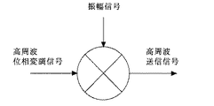
このような課題を解決するために、高電力効率に動作する送信装置として、ポーラ変調方式を用いた送信装置が提案されている。ポーラ変調方式とは、ベースバンド信号を振幅信号と位相信号とに分離後、振幅変調及び位相変調を独立に施すものである(例えば、図10参照)。図10の例では、位相信号に基づいて位相変調された高周波位相変調信号と、振幅信号とを乗算器で乗算して、高周波送信信号を生成している。ポーラ変調方式を用いた送信装置は、乗算器の役割を果たす高周波電力増幅器を非線形動作(飽和動作)させることができるので、電力効率を向上させることができる。この種のポーラ変調方式を用いた技術は、例えば、特許文献1や特許文献2に記載されている。
In order to solve such a problem, a transmitter using a polar modulation scheme has been proposed as a transmitter that operates with high power efficiency. In the polar modulation method, a baseband signal is separated into an amplitude signal and a phase signal, and then amplitude modulation and phase modulation are performed independently (see, for example, FIG. 10). In the example of FIG. 10, the high frequency phase modulation signal phase-modulated based on the phase signal and the amplitude signal are multiplied by a multiplier to generate a high frequency transmission signal. The transmission apparatus using the polar modulation method can improve the power efficiency because the high-frequency power amplifier serving as a multiplier can perform a non-linear operation (saturation operation). Techniques using this type of polar modulation method are described in, for example,
図11は、ポーラ変調方式を用いた従来の送信装置500の機能ブロックの一例を示す図である。図11において、従来の送信装置500は、振幅位相分離部501、乗算器502、振幅信号増幅器503、位相変調部504、可変利得増幅器505、高周波電力増幅器506、ディジタル−アナログ変換器(以降、D/A変換部と記す)507、及びディジタル−アナログ変換器(以降、D/A変換部と記す)508を備える。
FIG. 11 is a diagram illustrating an example of functional blocks of a conventional transmission device 500 using a polar modulation scheme. In FIG. 11, a conventional transmission apparatus 500 includes an amplitude
振幅位相分離部501は、入力された変調用ベースバンド信号S51を振幅信号S52と位相信号S53とに分離する。乗算器502には、振幅信号S52と、送信電力の大きさを制御するための送信電力制御信号S54とが入力される。乗算器502は、振幅信号S52と送信電力制御信号S54とを乗算し、送信電力制御された振幅信号S55として出力する。振幅信号S55は、D/A変換器507でアナログ信号S56に変換され、振幅信号増幅器503を介して、非線形動作(飽和動作)する高周波電力増幅器506に電源電圧S57として供給される。
The amplitude
一方、位相信号S53は、位相変調部504に入力される。位相変調部504は、位相信号S53で搬送波信号を位相変調し、位相変調した信号を高周波位相変調信号S58として出力する。高周波位相変調信号S58は、可変利得増幅器505に入力される。可変利得増幅器505の利得は、制御部(図示せず)からの利得制御ディジタル信号S61をD/A変換したアナログ信号S62によって制御される。可変利得増幅器505は、高周波位相変調信号S58を増幅し、高周波位相変調信号S59として出力する。高周波位相変調信号S59は、高周波電力増幅器506に入力される。高周波電力増幅器506は、振幅信号増幅器503から供給された電源電圧S57に基づいて、高周波位相変調信号S59に対して振幅変調を施して、高周波送信信号S60として出力する。
On the other hand, the phase signal S53 is input to the
次に、従来の送信信装置500の動作について、数式を用いて詳しく説明する。まず、変調用ベースバンド信号S1をSi(t)とすると、Si(t)は、複素数表示を用いて式(1)で表すことができる。 Next, the operation of the conventional transmission apparatus 500 will be described in detail using mathematical expressions. First, assuming that the modulation baseband signal S1 is Si (t), Si (t) can be expressed by Expression (1) using a complex number display.
Si(t)=a(t)・exp[jφ(t)] ・・・・・ (1)
ここで、a(t)は振幅データを、exp[jφ(t)]は位相データをそれぞれ示す。振幅位相分離部501は、変調用ベースバンド信号Si(t)から振幅データa(t)と、位相データexp[jφ(t)]とを抽出する。ここで、振幅データa(t)は振幅信号S52に、位相データexp[jφ(t)]は位相信号S53にそれぞれ対応する。振幅データa(t)は、乗算器502で送信電力制御信号S54が示す電力情報Gと乗算され、送信電力制御された振幅データG・a(t)として出力される。振幅データG・a(t)は、振幅信号増幅器503で増幅され、高周波電力増幅器506に電源電圧として供給される。
Si (t) = a (t) · exp [jφ (t)] (1)
Here, a (t) represents amplitude data, and exp [jφ (t)] represents phase data. The amplitude
位相変調部504は、角周波数ωcの搬送波を位相データexp[jφ(t)]で変調して、高周波位相変調信号S58を生成する。ここで、高周波位相変調信号S58をScとすると、Scは式(2)で表すことができる。
The
Sc=exp[j(ωc×t+φ(t))] ・・・・・ (2)
そして、高周波電力増幅器506は、上述した振幅データG・a(t)と、可変利得増幅器505を介して入力された高周波位相変調信号S59とを乗算し、高周波送信信号S60として出力する。高周波送信信号S60をRF信号Srfとすると、RF信号Srtは式(3)で表すことができる。
Sc = exp [j (ωc × t + φ (t))] (2)
The high-
Srf=G・a(t)・exp[j(ωc×t+φ(t))] ・・・・(3)
ポーラ変調方式を用いた従来の送信信装置500は、高周波電力増幅器506が出力する信号の振幅(包絡線)を電源電圧で制御するため、高周波電力増幅器506を飽和動作させることができるので電力効率を高くすることができる。
Since the conventional transmission apparatus 500 using the polar modulation method controls the amplitude (envelope) of the signal output from the high-
しかしながら、従来のポーラ変調送信装置500においては、以下に述べるような課題を有していた。 However, the conventional polar modulation transmission apparatus 500 has the following problems.
送信電力のダイナミックレンジは、無線通信方式によって異なるが、低出力側のダイナミックレンジの方が広くなる場合、すなわち、送信電力の最小値が小さな無線通信方式においては、振幅信号として微少な信号が要求される。従って、従来のポーラ変調送信装置500においては、送信電力制御後の振幅信号55に、微小信号が要求されることになる。
The dynamic range of transmission power differs depending on the wireless communication system, but when the dynamic range on the low output side becomes wider, that is, in the wireless communication system with a small minimum transmission power, a small signal is required as an amplitude signal. Is done. Therefore, in the conventional polar modulation transmission apparatus 500, a minute signal is required for the
図12は、送信電力の大小による振幅信号S55の変化範囲の違いを示す図である。図12において、横軸は、振幅信号S55をボルト(V)単位に真数で示したものであり、送信電力の大小による振幅信号S55の変化範囲を連続信号として矢印で表している。横軸の目盛は、振幅信号S55をディジタル信号で表現した場合に値が離散化(量子化)されることを模式的に示している。このように、真数表現された振幅信号S55をディジタル信号として扱った場合、送信電力が小さい場合に振幅信号S55の変化範囲に対する量子化ノイズの割合が大きくなることがわかる。すなわち、送信電力が小さい場合、量子化ノイズによって振幅信号S55の表現精度が悪くなり、これが送信信号の歪みを表すACLR(Adjacent Channel Leakage power Ratio)や、変調精度を表すEVM(Error Vector Magnitude)を劣化させることになる。 FIG. 12 is a diagram illustrating a difference in the change range of the amplitude signal S55 depending on the transmission power. In FIG. 12, the horizontal axis indicates the amplitude signal S55 in a true number in volts (V), and the change range of the amplitude signal S55 depending on the magnitude of the transmission power is represented by an arrow as a continuous signal. The scale on the horizontal axis schematically shows that the value is discretized (quantized) when the amplitude signal S55 is expressed as a digital signal. As described above, when the amplitude signal S55 expressed as a true number is handled as a digital signal, the ratio of the quantization noise to the change range of the amplitude signal S55 increases when the transmission power is small. That is, when the transmission power is small, the representation accuracy of the amplitude signal S55 is deteriorated due to the quantization noise, and this causes an ACLR (Adjacent Channel Leakage power Ratio) representing distortion of the transmission signal and an EVM (Error Vector Magnitude) representing modulation accuracy. It will deteriorate.
真数表現した振幅信号S55をディジタル信号として扱った場合の量子化ノイズがACLR及びEVMに及ぼす影響をシミュレーションした結果を、図13及び図14にそれぞれ示す。図13は、量子化ノイズがACLRに及ぼす影響をシミュレーションした結果を示す図である。図14は、量子化ノイズがEVMに及ぼす影響をシミュレーションした結果を示す図である。なお、シミュレーションには、EDGE(Enhanced Data GSM Environment)変調信号を用いた。 The simulation results of the influence of quantization noise on ACLR and EVM when the amplitude signal S55 expressed as a true number is handled as a digital signal are shown in FIGS. 13 and 14, respectively. FIG. 13 is a diagram illustrating a result of simulating the influence of quantization noise on ACLR. FIG. 14 is a diagram illustrating a result of simulating the influence of quantization noise on the EVM. In the simulation, an EDGE (Enhanced Data GSM Environment) modulation signal was used.
図13において、ACLRは、400kHz離調の結果(図13(a)参照)、及び600kHz離調の結果(図13(b)参照)を示している。また、図14において、EVMは、3GPP(3rd Generation Partnership Project)の標準規格におけるRMS EVMを表す。量子化のビット数は14ビット、12ビット、10ビット、8ビットの4種類でシミュレーションを行った。また、量子化ノイズの影響を見るためにポーラ変調が行われる最終段の高周波電力増幅部506の特性は、理想的な線形特性(歪みなし)と仮定した。
In FIG. 13, ACLR indicates the result of 400 kHz detuning (see FIG. 13A) and the result of 600 kHz detuning (see FIG. 13B). In FIG. 14, EVM represents RMS EVM in the standard of 3GPP (3rd Generation Partnership Project). The simulation was performed with four types of quantization bits of 14 bits, 12 bits, 10 bits, and 8 bits. Further, in order to see the influence of quantization noise, the characteristic of the high-
図13及び図14に示すように、真数表現した振幅信号S55をディジタル信号として扱った場合、送信電力が小さくなるにしたがって、ACLRやEVMが劣化することがわかる。また、同じ送信電力で比較した場合、量子化のビット数が小さいほどACLRやEVMの劣化が大きいことがわかる。 As shown in FIGS. 13 and 14, when the amplitude signal S55 expressed as a true number is handled as a digital signal, it is understood that the ACLR and EVM deteriorate as the transmission power decreases. Further, when comparing with the same transmission power, it can be seen that the smaller the number of bits of quantization, the greater the degradation of ACLR and EVM.
上述した説明では、振幅信号S55をディジタル信号として扱った場合の量子化ノイズに起因するACLRやEVMの劣化について説明したが、振幅信号S55をアナログ信号として扱った場合にも、振幅信号S55が微小になるとSN比(信号対雑音比)が劣化するので、定性的には上記と同様にACLRやEVMの劣化が見られる。 In the above description, degradation of ACLR and EVM caused by quantization noise when the amplitude signal S55 is handled as a digital signal has been described. However, when the amplitude signal S55 is handled as an analog signal, the amplitude signal S55 is very small. Since the SN ratio (signal-to-noise ratio) is degraded, the ACLR and EVM are degraded qualitatively as described above.
それ故に本発明の目的は、上記課題を解決するものであり、送信電力のダイナミックレンジが広い変調方式においても、低出力まで変調精度や歪み特性を良好に維持し、かつ電力効率が良好なポーラ変調送信装置を提供することである。 Therefore, an object of the present invention is to solve the above-mentioned problems. Even in a modulation scheme with a wide dynamic range of transmission power, a polar system that maintains good modulation accuracy and distortion characteristics up to low output and has good power efficiency. A modulation transmission apparatus is provided.
本発明は、ポーラ変調送信装置に向けられている。そして、上記目的を達成させるために、本発明のポーラ変調送信装置は、変調用ベースバンド信号を振幅信号と位相信号とに分離する振幅位相分離部と、振幅信号を真数/対数変換し、対数表現された振幅信号として出力する第1の真数/対数変換部と、送信電力制御信号を真数/対数変換し、対数表現された送信電力制御信号として出力する第2の真数/対数変換部と、対数表現された振幅信号に、対数表現された送信電力制御信号を加算し、送信電力制御された振幅信号として出力する加算器と、送信電力制御された振幅信号を対数/真数変換し、真数表現された振幅信号として出力する対数/真数変換部と、位相信号に基づいて高周波搬送波信号に位相変調を施して、高周波位相変調信号として出力する位相変調部と、供給される電源電圧に基づいて高周波位相変調信号に対して振幅変調を施して、高周波送信信号として出力する高周波電力増幅器と、真数表現された振幅信号を増幅し、増幅した振幅信号を電源電圧として高周波電力増幅器へ供給する振幅信号増幅器とを備える。 The present invention is directed to a polar modulation transmission apparatus. In order to achieve the above object, the polar modulation transmission apparatus of the present invention includes an amplitude phase separation unit that separates a modulation baseband signal into an amplitude signal and a phase signal, and performs a true / logarithmic conversion of the amplitude signal, A first logarithm / logarithm conversion unit that outputs as a logarithmically expressed amplitude signal, and a second logarithm / logarithm that outputs the logarithmically expressed transmit power control signal by performing logarithm / logarithm conversion on the transmission power control signal A conversion unit, an adder that adds a logarithmically expressed transmission power control signal to a logarithmically expressed amplitude signal, and outputs the resultant signal as a transmission power controlled amplitude signal; A logarithm / integer conversion unit that converts and outputs as an amplitude signal expressed as a true number; a phase modulation unit that performs phase modulation on the high frequency carrier signal based on the phase signal and outputs the phase modulation signal; Power supply A high-frequency power amplifier that performs amplitude modulation on a high-frequency phase-modulated signal based on the pressure and outputs it as a high-frequency transmission signal, amplifies the amplitude signal expressed as a true number, and uses the amplified amplitude signal as a power supply voltage And an amplitude signal amplifier to be supplied.
これによって、ポーラ変調送信装置は、送信電力が小さく振幅信号が小さい場合でも量子化ノイズやSN比(信号雑音比)の悪化による振幅信号の表現精度の劣化を抑制し、ACLRやEVMの劣化を抑制することができる。また、振幅信号と送信電力制御信号とを乗算するための乗算器を備える必要がないので、回路規模を大幅に削減することができる。 As a result, the polar modulation transmission apparatus suppresses deterioration of the representation accuracy of the amplitude signal due to deterioration of quantization noise and SN ratio (signal-to-noise ratio) even when the transmission power is small and the amplitude signal is small, and deterioration of ACLR and EVM is suppressed. Can be suppressed. Moreover, since it is not necessary to provide a multiplier for multiplying the amplitude signal and the transmission power control signal, the circuit scale can be greatly reduced.
好ましくは、高周波電力増幅器は、非線形増幅器として動作し、高周波位相変調信号に対して、送信電力制御信号及び振幅信号に応じた振幅変調を施す。 Preferably, the high frequency power amplifier operates as a non-linear amplifier, and performs amplitude modulation on the high frequency phase modulation signal according to the transmission power control signal and the amplitude signal.
好ましくは、ポーラ変調送信装置は、位相変調部の後段に、制御された利得で高周波位相変調信号を増幅する可変利得増幅器をさらに備える。 Preferably, the polar modulation transmission apparatus further includes a variable gain amplifier that amplifies the high-frequency phase modulation signal with a controlled gain, following the phase modulation unit.
好ましくは、振幅信号増幅器は、スイッチングレギュレータ、又はD級増幅器から構成される。これによって、振幅信号用増幅器の電力効率を向上させることができる。また、送信装置全体としても電力効率を向上させることができる。 Preferably, the amplitude signal amplifier includes a switching regulator or a class D amplifier. As a result, the power efficiency of the amplitude signal amplifier can be improved. In addition, the power efficiency of the entire transmission device can be improved.
また、ポーラ変調送信装置は、加算器と対数/真数変換部との間に、送信電力調整用の第2の加算器をさらに備えてもよい。第2の加算器は、電力制御された振幅信号に利得調整用の値を加算する。これによって、出力パワーの個体ばらつきを製造時に容易に調整したり、振幅信号の利得を調整することが可能となる。
る。
The polar modulation transmission apparatus may further include a second adder for adjusting transmission power between the adder and the logarithm / integer conversion unit. The second adder adds a gain adjustment value to the power-controlled amplitude signal. As a result, individual variations in output power can be easily adjusted at the time of manufacture, and the gain of the amplitude signal can be adjusted.
The
また、振幅信号増幅器は、送信電力の大きさに応じて、高周波電力増幅器に、振幅信号及び送信電力制御信号に応じた電源電圧か、あるいは所定の固定値電源電圧のいずれかを選択的に供給してもよい。振幅信号及び送信電力制御信号に応じた電源電圧が選択された場合には、高周波電力増幅器は、非線形増幅器として動作し、可変利得増幅器で増幅された高周波位相変調信号に対して、送信電力制御信号及び振幅信号に応じた振幅変調を施して、高周波送信信号として出力する。一方、所定の固定値電源電圧が選択された場合には、可変利得増幅器は、位相変調部が出力した高周波位相変調信号に対して、送信電力制御信号及び振幅信号に応じた振幅変調を施す。高周波電力増幅器は、線形増幅器として動作し、可変利得増幅器が振幅変調を施した信号を所定の固定値電源電圧に応じた一定の利得で増幅し、高周波送信信号として出力する。 The amplitude signal amplifier selectively supplies either a power supply voltage corresponding to the amplitude signal and the transmission power control signal or a predetermined fixed value power supply voltage to the high frequency power amplifier according to the magnitude of the transmission power. May be. When the power supply voltage corresponding to the amplitude signal and the transmission power control signal is selected, the high frequency power amplifier operates as a non-linear amplifier, and the transmission power control signal is applied to the high frequency phase modulation signal amplified by the variable gain amplifier. Then, amplitude modulation according to the amplitude signal is performed and output as a high-frequency transmission signal. On the other hand, when a predetermined fixed value power supply voltage is selected, the variable gain amplifier performs amplitude modulation according to the transmission power control signal and the amplitude signal on the high-frequency phase modulation signal output from the phase modulation unit. The high-frequency power amplifier operates as a linear amplifier, amplifies the signal subjected to amplitude modulation by the variable gain amplifier with a constant gain according to a predetermined fixed value power supply voltage, and outputs the amplified signal as a high-frequency transmission signal.
これによって、ポーラ変調送信装置は、送信電力の大きさに応じて、高周波電力増幅器で振幅変調を行うか、可変利得増幅器で振幅変調を行うかを選択することができる。このため、ポーラ変調送信装置は、送信電力の範囲に係わらず、送信信号の歪み特性及び変調精度を良好に保つことができる。 Accordingly, the polar modulation transmission apparatus can select whether to perform amplitude modulation with the high-frequency power amplifier or to perform amplitude modulation with the variable gain amplifier according to the magnitude of the transmission power. For this reason, the polar modulation transmission apparatus can maintain good distortion characteristics and modulation accuracy of the transmission signal regardless of the transmission power range.
好ましくは、ポーラ変調送信装置は、加算器と可変利得増幅器との間に、送信電力調整用の第3の加算器をさらに備える。第3の加算器は、送信電力制御された振幅信号に利得調整用の値を加算する。これによって、高周波電力増幅器と、可変利得増幅器との違いによる振幅信号に対する利得の差を調整することができる。また、可変利得増幅器の個体ばらつきを製造時に調整することが可能となる。 Preferably, the polar modulation transmission apparatus further includes a third adder for adjusting transmission power between the adder and the variable gain amplifier. The third adder adds a gain adjustment value to the transmission power-controlled amplitude signal. As a result, the gain difference with respect to the amplitude signal due to the difference between the high-frequency power amplifier and the variable gain amplifier can be adjusted. Also, individual variations of the variable gain amplifier can be adjusted at the time of manufacture.
好ましくは、ポーラ変調送信装置は、対数/真数変換部の前段までのいずれかの位置に、D/A変換器をさらに備える。対数/真数変換部には、D/A変換器を経由したアナログ信号が入力される。これによって、対数/真数変換部は、バイポーラトランジスタのアナログ入出力の指数関数特性を利用することにより、比較的簡単に対数/真数変換を実現することができる。また、ディジタル回路において小信号で顕著となる量子化ノイズの影響を抑制することができ、振幅信号を対数表現する効果をより顕著なものにすることができる。 Preferably, the polar modulation transmission apparatus further includes a D / A converter at any position up to the previous stage of the logarithm / integer conversion unit. An analog signal that has passed through the D / A converter is input to the logarithm / integer conversion unit. As a result, the logarithm / logarithm conversion unit can realize logarithm / logarithm conversion relatively easily by utilizing the exponential characteristic of the analog input / output of the bipolar transistor. In addition, it is possible to suppress the influence of quantization noise that becomes noticeable with a small signal in a digital circuit, and to make the effect of logarithmically expressing an amplitude signal more remarkable.
また、ポーラ変調送信装置は、高周波電力増幅器の前段までのいずれかの位置に接続され、少なくとも高周波電力増幅器で発生する歪みが抑圧されるように、予め高周波電力増幅器に電源電圧として供給される振幅信号を歪ませる歪み補償部をさらに備えてもよい。これによって、ポーラ変調送信装置は、より低歪みな動作を実現することができる。 The polar modulation transmitter is connected to any position up to the preceding stage of the high-frequency power amplifier, and the amplitude supplied in advance as a power supply voltage to the high-frequency power amplifier so that at least distortion generated in the high-frequency power amplifier is suppressed. You may further provide the distortion compensation part which distorts a signal. Thereby, the polar modulation transmission apparatus can realize an operation with lower distortion.
また、本発明は、無線通信装置にも向けられている。無線通信装置は、送信信号を生成する送信回路と、送信回路で生成された送信信号を出力するアンテナとを備える。送信回路には、上述したポーラ変調送信装置が用いられる。また、無線通信装置は、アンテナから受信した受信信号を処理する受信回路と、送信回路で生成された送信信号をアンテナに出力し、アンテナから受信した受信信号を受信回路に出力するアンテナ共用部とをさらに備えてもよい。 The present invention is also directed to a wireless communication device. The wireless communication device includes a transmission circuit that generates a transmission signal and an antenna that outputs the transmission signal generated by the transmission circuit. The polar modulation transmission apparatus described above is used for the transmission circuit. In addition, the wireless communication device includes a reception circuit that processes a reception signal received from the antenna, an antenna sharing unit that outputs the transmission signal generated by the transmission circuit to the antenna, and outputs the reception signal received from the antenna to the reception circuit; May be further provided.
これによって、無線通信装置は、送信回路の送信電力の制御範囲を広くでき、低出力まで変調精度や歪み特性を良好に維持できるため、広い送信電力に亘って優れたACLRやEVMの特性を実現することができる。また、送信回路の電力効率が高いため、搭載している電池電源の使用時間を延ばすことができる。 As a result, the wireless communication device can widen the control range of the transmission power of the transmission circuit, and can maintain the modulation accuracy and distortion characteristics well up to a low output, thereby realizing excellent ACLR and EVM characteristics over a wide transmission power. can do. In addition, since the power efficiency of the transmission circuit is high, it is possible to extend the usage time of the mounted battery power supply.
以上のように、本発明のポーラ変調送信装置においては、真数/対数変換部が、振幅信号及び送信電力制御信号を真数/対数変換し、対数表現された振幅信号及び対数表現された送信電力制御信号として出力する。これによって、ポーラ変調送信装置は、加算器で対数表現された振幅信号と、対数表現された送信電力制御信号とを加算するだけで、振幅信号に対する送信電力制御を実現することができる。また、送信装置は、振幅信号と送信電力制御信号とを乗算するための乗算器を備える必要がないので、回路規模を大幅に削減することができる。 As described above, in the polar modulation transmission apparatus of the present invention, the logarithm / logarithm conversion unit performs logarithm / logarithm conversion on the amplitude signal and the transmission power control signal, and the logarithmically expressed amplitude signal and logarithmically expressed transmission. Output as a power control signal. Thus, the polar modulation transmission apparatus can realize transmission power control for the amplitude signal only by adding the logarithmically expressed amplitude signal and the logarithmically expressed transmission power control signal. Further, since the transmission apparatus does not need to include a multiplier for multiplying the amplitude signal and the transmission power control signal, the circuit scale can be greatly reduced.
また、ポーラ変調送信装置は、対数表現された振幅信号を扱うので、送信電力の大小に係わらず、振幅信号の変化範囲に対する量子化ノイズの割合が等しくなる。このため、ポーラ変調送信装置は、送信電力が小さく振幅信号が小さい場合であっても量子化ノイズやSN比(信号雑音比)の悪化による振幅信号の表現精度の劣化を抑制し、ACLRやEVMの劣化を防ぐことができる。これによって、ポーラ変調送信装置は、送信電力のダイナミックレンジが広い変調方式においても、低出力まで変調精度や歪み特性を良好に維持し、かつ高い電力効率を実現することができる。 Further, since the polar modulation transmission apparatus handles logarithmically expressed amplitude signals, the ratio of quantization noise to the amplitude signal change range becomes equal regardless of the magnitude of transmission power. For this reason, the polar modulation transmission apparatus suppresses the deterioration of the representation accuracy of the amplitude signal due to the deterioration of the quantization noise and the SN ratio (signal-to-noise ratio) even when the transmission power is small and the amplitude signal is small, and ACLR and EVM are suppressed. Can be prevented. As a result, the polar modulation transmission apparatus can maintain good modulation accuracy and distortion characteristics up to a low output and achieve high power efficiency even in a modulation system with a wide dynamic range of transmission power.
本発明のこれらおよび他の目的、特徴、局面、効果は、添付図面と照合して、以下の詳細な説明から一層明らかになるであろう。 These and other objects, features, aspects and advantages of the present invention will become more apparent from the following detailed description when taken in conjunction with the accompanying drawings.
以下、本発明の各実施形態について図面を参照しながら詳細に説明する。 Hereinafter, embodiments of the present invention will be described in detail with reference to the drawings.
(第1の実施形態)
図1は、本発明の第1の実施形態に係るポーラ変調送信装置100の概略構成の一例を示すブロック図である。図1において、ポーラ変調送信装置(以下、単に送信装置と記す)100は、振幅位相分離部101、加算器102、振幅信号増幅器103、位相変調部104、可変利得増幅器105、高周波電力増幅器106、D/A変換器107、D/A変換器108、真数/対数変換部109、真数/対数変換部110、及び対数/真数変換部111を備える。
(First embodiment)
FIG. 1 is a block diagram showing an example of a schematic configuration of a polar
送信装置100は、変調用ベースバンド信号S1をポーラ変調方式を用いて変調し、高周波送信信号S10として出力する。以下、送信装置100の動作の詳細について説明する。変調用ベースバンド信号S1は、振幅位相分離部101にデジタル信号として入力される。振幅位相分離部101は、入力された変調用ベースバンド信号S1を振幅信号S2と位相信号S3とに分離する。
The
振幅信号S2は、真数/対数変換部110に入力される。真数/対数変換部110は、入力された振幅信号S2を真数/対数変換し、対数表現された振幅信号S14として出力する。真数/対数変換部109には、送信電力の大きさを制御するための送信電力制御信号S4が入力される。真数/対数変換部109は、送信電力制御信号S4を真数/対数変換し、対数表現された送信電力制御信号S13として出力する。真数/対数変換部109、110は、論理演算を行うデジタル回路によって真数/対数変換を実現してもよいし、入出力(真数/対数)の関係を定義したROMテーブル等を用いて真数/対数変換を実現してもよい。
The amplitude signal S2 is input to the true /
送信電力制御信号S13と、振幅信号S14とは、加算器102に入力される。加算器102は、振幅信号S14に、送信電力制御信号S13を加算し、送信電力制御された振幅信号S5として出力する。振幅信号S5は、D/A変換器107でアナログ信号S16に変換される。なお、送信装置100は、D/A変換器107の後にローパスフィルタ(図示せず)を備えてもよい。
The transmission power control signal S13 and the amplitude signal S14 are input to the
アナログ信号S16は、対数/真数変換部111で対数/真数変換され、真数表現された振幅信号S6として出力される。振幅信号S6は、振幅信号増幅器103で電流駆動能力を増幅されて、高周波電力増幅器106に電源電圧S7として供給される。ここで、振幅信号増幅器103は、電力効率を高めるために、スイッチングレギュレータやD級増幅器から構成されることが好ましい。
The analog signal S16 is logarithm / logarithmically converted by the logarithm /
一方、位相信号S3は、位相変調部104に入力される。位相変調部104は、位相信号S3に基づいて搬送波信号に位相変調を施して、高周波位相変調信号S8として出力する。高周波位相変調信号S8は、可変利得増幅器105に入力される。可変利得増幅器105の利得は、制御部(図示せず)からのディジタル信号S11をD/A変換したアナログ信号S12によって制御される。可変利得増幅器105は、高周波位相変調信号S8を増幅し、高周波位相変調信号S9として出力する。
On the other hand, the
高周波位相変調信号S9は、高周波電力増幅器106に入力される。高周波電力増幅器106は、振幅信号増幅器103から電源電圧として供給された振幅信号S7に基づいて、高周波変調信号S9に対して振幅変調を施して、高周波送信信号S10として出力する。
The high frequency phase modulation signal S9 is input to the high
送信装置100は、対数表現された振幅信号S14及び対数表現された送信電力制御信号S13を扱うので、本来なら乗算器が必要となる送信電力制御に伴う演算を加算器102で行うことができる。このため、送信装置100は、乗算器を備える必要がなくなり、回路規模を大幅に縮小することができる。
Since the
また、送信電力制御された振幅信号S5は、対数表現されているので、真数表現されている場合には微小な値であっても、大きな値である場合と同じ変化範囲で表現することができる。図2は、送信電力の大小による振幅信号S5の変化範囲の違いを示す図である。図2において、横軸は、振幅信号S5をdBV単位に対数で示したものであり、送信電力の大小による振幅信号S5の変化範囲を連続信号として矢印で表している。横軸の目盛は、振幅信号S5をディジタル信号で表現した場合に値が離散化(量子化)されることを模式的に示している。 Further, since the amplitude signal S5 subjected to transmission power control is expressed logarithmically, even if it is expressed as a true number, even a minute value can be expressed in the same change range as when it is a large value. it can. FIG. 2 is a diagram illustrating the difference in the change range of the amplitude signal S5 depending on the magnitude of the transmission power. In FIG. 2, the horizontal axis represents the amplitude signal S5 in a logarithm in dBV units, and the change range of the amplitude signal S5 depending on the magnitude of the transmission power is represented by an arrow as a continuous signal. The scale on the horizontal axis schematically shows that the value is discretized (quantized) when the amplitude signal S5 is expressed as a digital signal.
図2に示すように、対数表現された振幅信号S5をディジタル信号として扱った場合は、送信電力の大小に係わらず、振幅信号S5の変化範囲は等しくなり、振幅信号S5の変化範囲に対する量子化ノイズの割合も等しくなることがわかる。すなわち、送信電力が小さい場合も、量子化ノイズによって振幅信号S5の表現精度が悪くならず、送信信号の歪みを表すACLRや、変調精度を表すEVMの劣化を防ぐことができる。 As shown in FIG. 2, when the logarithmically expressed amplitude signal S5 is handled as a digital signal, the change range of the amplitude signal S5 is equal regardless of the magnitude of the transmission power, and the quantization with respect to the change range of the amplitude signal S5 is performed. It can be seen that the noise ratio is also equal. That is, even when the transmission power is small, the representation accuracy of the amplitude signal S5 is not deteriorated due to the quantization noise, and the degradation of the ACLR indicating the distortion of the transmission signal and the EVM indicating the modulation accuracy can be prevented.
対数表現した振幅信号S5をディジタル信号として扱った場合の量子化ノイズがACLR及びEVMに及ぼす影響をシミュレーションした結果を、図3及び図4にそれぞれ示す。図3は、量子化ノイズがACLRに及ぼす影響をシミュレーションした結果を示す図である。図4は、量子化ノイズがEVMに及ぼす影響をシミュレーションした結果を示す図である。なお、シミュレーションには、EDGE変調信号を用いた。 The results of simulating the influence of quantization noise on ACLR and EVM when the logarithmically expressed amplitude signal S5 is handled as a digital signal are shown in FIGS. 3 and 4, respectively. FIG. 3 is a diagram illustrating a result of simulating the influence of quantization noise on ACLR. FIG. 4 is a diagram illustrating a result of simulating the influence of quantization noise on the EVM. In the simulation, an EDGE modulation signal was used.
図3において、ACLRは、400kHz離調の結果(図3(a)参照)、及び600kHz離調の結果(図3(b)参照)を示しており、EVMは3GPP(3rd Generation Partnership Project)の標準規格におけるRMS EVMを表す。量子化のビット数は、14ビット、12ビット、10ビット、8ビットの4種類でシミュレーションを行った。また、量子化ノイズの影響を見るためにポーラ変調が行われる最終段の高周波電力増幅器106の特性は理想的な線形特性(歪み無し)と仮定した。
In FIG. 3, ACLR shows the result of 400 kHz detuning (see FIG. 3 (a)) and 600kHz detuning (see FIG. 3 (b)), and EVM is the result of 3GPP (3rd Generation Partnership Project). Represents RMS EVM in the standard. The simulation was performed with four types of quantization bits of 14 bits, 12 bits, 10 bits, and 8 bits. In order to see the influence of the quantization noise, it is assumed that the characteristic of the high-
図3及び図4に示すように、対数表現した振幅信号S5をディジタル信号として扱った場合は、送信電力が小さくなっても、ACLRやEVMの劣化が見られないことがわかる。600kHz離調でのACLRは、量子化のビット数が大きいほど歪み量が小さくなっているが、これは歪み量の最小値が量子化ノイズによって制限されているためである。 As shown in FIGS. 3 and 4, when the logarithmically expressed amplitude signal S5 is handled as a digital signal, it can be seen that even when the transmission power is reduced, the ACLR and EVM are not deteriorated. In ACLR at 600 kHz detuning, the amount of distortion decreases as the number of bits for quantization increases. This is because the minimum value of the amount of distortion is limited by quantization noise.
上述した説明では、振幅信号S5をディジタル信号として扱った場合の量子化ノイズに起因するACLRやEVMの劣化について説明したが、振幅信号S5をアナログ信号として扱った場合にも、振幅信号S5が微小になるとSN比(信号対雑音比)が劣化するので、定性的には上記と同様にACLRやEVMの劣化が見られる。そのため、本発明の効果は、振幅信号S5をアナログ信号として扱った場合にも同様に得られる。なお、送信装置100は、振幅信号S5をアナログ信号として扱った場合は、D/A変換器107を備える必要がなくなる。
In the above description, degradation of ACLR and EVM caused by quantization noise when the amplitude signal S5 is handled as a digital signal has been described. However, when the amplitude signal S5 is handled as an analog signal, the amplitude signal S5 is very small. Since the SN ratio (signal-to-noise ratio) is degraded, the ACLR and EVM are degraded qualitatively as described above. Therefore, the effect of the present invention can be obtained similarly when the amplitude signal S5 is handled as an analog signal. The
また、本発明では、対数/真数変換部111の前段までの機能ブロック(振幅位相分離部101、真数/対数変換部109、110、及び加算部102など)がディジタル回路によって構成されることを想定しているが、これらの機能ブロックはアナログ回路によって構成されても構わない。そのため、D/A変換器107は、図1に示した位置だけでなく、任意の位置に接続される可能性がある。
In the present invention, the functional blocks up to the previous stage of the logarithm / true number conversion unit 111 (amplitude
ただし、対数/真数変換部111には、アナログ信号が入力されることが望ましい。その理由を以下に説明する。対数/真数変換部111は、バイポーラトランジスタのアナログ入出力の指数関数特性を利用することにより、比較的簡単に対数/真数変換を実現できる。そのため、対数/真数変換部111は、アナログ回路によって構成され、D/A変換後のアナログ信号が入力されることが望ましい。
However, it is desirable that an analog signal is input to the logarithm /
また、送信装置100は、送信電力制御信号S4及び振幅信号S2を真数/対数変換部109及び110で、真数/対数変換しているが、振幅位相分離部101や制御部(図示せず)から対数表現された振幅信号及び送信電力制御信号を直接加算器102に入力すれば、真数/対数変換部109及び110を備える必要がなくなり、回路規模を削減することができる。また、送信装置100は、高周波位相変調信号S8の大きさが適切である場合には、可変利得増幅器105及びD/A変換器108を必ずしも備えなくてもよい。
Further, although the
以上のように、本発明の第1の実施形態に係る送信装置100においては、真数/対数変換部110、109が、振幅信号S2及び送信電力制御信号S4を真数/対数変換し、対数表現された振幅信号S14及び対数表現された送信電力制御信号S13として出力する。これによって、送信装置100は、加算器102で対数表現された振幅信号S14と、対数表現された送信電力制御信号S13とを加算するだけで、振幅信号に対する送信電力制御を実現することができる。また、送信装置100は、振幅信号と送信電力制御信号とを乗算するための乗算器を備える必要がないので、回路規模を大幅に削減することができる。
As described above, in the
また、送信装置100は、対数表現された振幅信号を扱うので、送信電力の大小に係わらず、振幅信号の変化範囲に対する量子化ノイズの割合が等しくなる。このため、送信装置100は、送信電力が小さく振幅信号が小さい場合であっても量子化ノイズやSN比(信号雑音比)の悪化による振幅信号の表現精度の劣化を抑制し、ACLRやEVMの劣化を防ぐことができる。
Further, since the
(第2の実施形態)
図5は、本発明の第2の実施形態に係るポーラ変調送信装置200の概略構成の一例を示すブロック図である。図5において、ポーラ変調送信装置(以下、単に送信装置と記す)200は、第1の実施形態に係る送信装置100と比較して、加算器114、加算器115、スイッチ112、及びスイッチ113をさらに備える。
(Second Embodiment)
FIG. 5 is a block diagram showing an example of a schematic configuration of a polar modulation transmission apparatus 200 according to the second embodiment of the present invention. In FIG. 5, a polar modulation transmission apparatus (hereinafter simply referred to as a transmission apparatus) 200 includes an
送信装置200は、変調用ベースバンド信号S1をポーラ変調方式を用いて変調し、高周波送信信号S10として送信する。以下、送信装置200の動作の詳細について説明する。ただし、第1の実施形態と同一のブロック及び信号については、同一の参照符号を付して説明を省略する。 The transmission device 200 modulates the modulation baseband signal S1 using a polar modulation method, and transmits the modulated baseband signal S1 as a high-frequency transmission signal S10. Details of the operation of the transmission apparatus 200 will be described below. However, the same blocks and signals as those in the first embodiment are denoted by the same reference numerals and description thereof is omitted.
送信装置200は、第1の実施形態に係る送信装置100と異なり、送信電力が大きい場合には高周波電力増幅器106で振幅変調を行い、送信電力が小さい場合には可変利得増幅器105で振幅変調を行う。
Unlike the
送信電力が大きい場合は、高周波電力増幅器106を非線形増幅器として(非線形モードで)動作させた方が電力効率の観点から望ましい。一方、送信電力が小さく、高周波電力増幅器106が非線形増幅器として動作可能な範囲から外れる場合は、高周波電力増幅器106を線形増幅器として(線形モードで)動作させた方が望ましい。
When the transmission power is large, it is desirable to operate the high-
高周波電力増幅器106をどちらのモードで動作させるかは、制御部(図示せず)によって、例えば、無線基地局からの送信電力制御信号や、受信信号の状態に基づく送信電力に応じて決定される。
Which mode the high-
図5において、スイッチ112及び113は、送信電力の大きさに応じて制御部から出力された切り替え信号S21によって、端子a−cと、端子b−cとの接続を切り替える。送信装置200は、送信電力の大きさに基づいてスイッチ112及び113の接続を切り替えることで、送信電力が大きい場合は高周波電力増幅器106で振幅変調を行い、送信電力が小さい場合は可変利得増幅器105で振幅変調を行う。また、加算器114及び115は、加算器102が出力する振幅信号S5に、制御部からそれぞれ信号S17及びS18で与えられる所定の値を加える。
In FIG. 5, switches 112 and 113 switch the connection between the terminals ac and bc by a switching signal S21 output from the control unit according to the magnitude of transmission power. The transmission apparatus 200 switches the connection between the
ここで、加算器114及び115の役割について詳しく説明する。高周波電力増幅器106で振幅変調を行う場合と、可変利得増幅器105で振幅変調を行う場合とでは、一般的に振幅信号S5に対する利得が異なるので、加算器114及び115は、必要に応じて、振幅信号S5に所定の値(一定値)を加えて、振幅信号S5に対する利得を調整する。また、加算器114及び115は、高周波電力増幅器106や可変利得増幅器105の個体ばらつきに起因する出力パワーのばらつきを調整する目的で使用することもできる。
Here, the role of the
まず、送信電力が大きく高周波電力増幅器106で振幅変調を行う場合は、スイッチ112及びスイッチ113は、それぞれ端子bと端子cとを接続する。可変利得増幅器105の利得は、制御部(図示せず)からのディジタル信号S19をD/A変換したアナログ信号S12によって制御される。可変利得増幅器105は、高周波位相変調信号S8を増幅し、高周波位相変調信号S9として出力する。高周波電力増幅器106は、振幅信号増幅器103から電源電圧として供給された振幅信号S7で、高周波変調信号S9に対して振幅変調を施して、高周波送信信号S10として出力する。
First, when the transmission power is large and amplitude modulation is performed by the high-
次に、送信電力が小さく可変利得増幅器105で振幅変調を行う場合は、スイッチ112及びスイッチ113は、それぞれ端子aと端子cとを接続する。その結果、可変利得増幅器105には、スイッチ113を介して、振幅信号S5がD/A変換されたアナログ信号S12が入力される。可変利得増幅器105は、高周波位相変調信号S8に対して、入力されたアナログ信号S12に応じた振幅変調を施す。すなわち、可変利得増幅器105は、高周波位相変調信号S8に対して、送信電力制御信号S4及び振幅信号S2に応じた振幅変調を施す。
Next, when the transmission power is small and amplitude modulation is performed by the
また、振幅信号増幅器103には、スイッチ112を介して、制御部(図示せず)から固定電圧値信号S20として、所定の固定電圧値を示す信号が入力される。固定電圧値信号S20は、振幅信号増幅器103で増幅されて、高周波電力増幅器106に電源電圧として供給される。このため、高周波電力増幅器106は、線形増幅器として動作し、可変利得増幅器105で振幅変調された高周波位相変調信号S9を一定の利得で増幅し、高周波送信信号S10として出力する。
A signal indicating a predetermined fixed voltage value is input to the
ここで、一般的な可変利得増幅器の特性について説明する。一般的な可変利得増幅器では、入力−出力間の電圧利得Vout/Vinが、利得制御信号の指数関数となる。このような可変利得増幅器の回路図の一例を図6に示す。 Here, characteristics of a general variable gain amplifier will be described. In a general variable gain amplifier, the voltage gain V out / V in between the input and output is an exponential function of the gain control signal. An example of a circuit diagram of such a variable gain amplifier is shown in FIG.
図6において、Vinは差動入力信号、Voutは差動出力信号、Vdは(差動)利得制御信号、Vccは電源電圧を示す。REはエミッタ抵抗、RLは負荷抵抗である。差動入力信号Vinが入力される入力端子に接続されたトランジスタTr5、Tr6は、エミッタ接地されており、コレクタに差動電流Gm・Vinが流れる。ここで、Gmは式(4)で表すことができる。

ただし、室温において、VTは約26mVの値を持つ。 However, at room temperature, V T has a value of about 26 mV.
さらに、利得制御信号Vdが入力される入力端子に接続されたトランジスタTr1、Tr2、Tr3、Tr4によって、差動電流がVdに応じて分割され、負荷抵抗RLで電圧降下が発生する。その結果、入力−出力間の電圧利得Vout/Vinの関係は、式(5)のように表すことができる。
式(5)は、Vd/VT<<−1(すなわち、入力が十分小さいとき)は、式(6)のように近似できる。
すなわち、入力−出力間の電圧利得Vout/Vinは、利得制御信号Vdの指数関数になっている。 In other words, the input-output voltage gain V out / V in is an exponential function of the gain control signal V d .
図5に示した可変利得増幅器105もこの指数関数の特性を有している。そのため、可変利得増幅器105は、対数/真数変換機能を含んでいる。このため、送信装置200(図5参照)は、可変利得増幅器105の前段に、対数/真数変換部を備える必要がなく、回路規模を大きく削減することができる。
The
次に、どのような場合に高周波電力増幅器106が非線形増幅器として動作可能な範囲を外れるのかについて説明する。図7は、高周波電力増幅器106の回路構成の一例を示す図である。高周波電力増幅器106は、非線形増幅器120と、非線形増幅器120の入力側と出力側との間に接続された寄生容量121とで構成することができる。
Next, the case where the high
図8は、非線形増幅器として用いた場合の高周波電力増幅器106の電源電圧と出力電力との関係を示す図である。図8に示すように、出力電力が大きい場合は、電源電圧の二乗と出力電力とが比例するが、電源電圧を下げていくとある値以下では出力電力が下がらなくなる。この値は、非線形増幅器120の入力信号のレベル(可変利得増幅器105の出力信号のレベル)と、寄生容量121によって定まる入力信号からのリーク電力とによって決まる。このように、高周波電力増幅器106の電源電圧が極めて小さくなると、高周波電力増幅器106の入力からのリーク電力のために、電源電圧による線形性に優れた振幅変調が困難になることがわかる。
FIG. 8 is a diagram showing the relationship between the power supply voltage and output power of the high-
このような理由により、送信装置200は、送信電力が十分に小さい場合は、高周波電力増幅器106の前段の可変利得増幅器105において線形性に優れた振幅変調を行い、高周波電力増幅器106を線形増幅器として使用している。
For this reason, when the transmission power is sufficiently small, the transmission apparatus 200 performs amplitude modulation with excellent linearity in the
以上のように、本発明の第2の実施形態に係る送信装置200においては、送信電力が大きい場合には、高周波電力増幅器106を非線形増幅器として用いて振幅変調を行い、送信電力が小さい場合には、可変利得増幅器105で振幅変調を行い、高周波電力増幅器106を線形増幅器として用いる。これによって、送信装置200は、送信電力の範囲に係わらず、送信信号の歪み特性及び変調精度を良好に保つことができる。
As described above, in the transmission apparatus 200 according to the second embodiment of the present invention, when transmission power is large, amplitude modulation is performed using the high-
また、送信装置200は、第1の実施形態と同様に、真数/対数変換部110、109が、振幅信号S2及び送信電力制御信号S4を真数/対数変換し、対数表現された振幅信号S14及び対数表現された送信電力制御信号S13として出力するので、第1の実施形態と同様の効果を得ることができる。
Further, in the transmission device 200, as in the first embodiment, the true /
なお、送信装置200は、真数表現された振幅信号S2及び送信電力制御信号S4を真数/対数変換部110及び109で対数変換しているが、対数表現された振幅信号及び送信電力制御信号を振幅位相分離部101や制御部(図示せず)から直接加算器102に入力すれば、回路規模を削減することができる。
The transmitting apparatus 200 logarithmically converts the amplitude signal S2 and the transmission power control signal S4 expressed in the logarithm by the logarithm /
また、送信装置200は、高周波電力増幅器106で振幅変調を行う場合でも、前段の可変利得増幅器105で振幅変調を行ってもかまわない。この場合、高周波電力増幅器106の入力電力が振幅信号S2の瞬時電力に応じて変化するので、高周波電力増幅器106の送信電力を小さくしたい時には高周波電力増幅器106の入力電力も小さくなり、高周波電力増幅器106のリーク電力が低減するので、高周波電力増幅器106の線形動作範囲を広くとることができる。
Further, the transmission apparatus 200 may perform amplitude modulation with the
また、可変利得増幅器105は、上述したような入出力の関係が指数関数となるものである必要はない。可変利得増幅器105の入出力の関係が線形の場合は、送信装置200は、可変利得増幅器105の前段に、対数−真数変換部を設ければよい。
Further, the
また、上述した送信装置100、200は、送信電力の範囲に応じて、振幅信号S2及び送信電力制御信号S4を真数/対数変換するか否かを選択する構成であってもよい。例えば、送信装置100、200は、送信電力がある値よりも小さい場合だけ、振幅信号S2及び送信電力制御信号S4を真数―対数変換する構成であってもよい。
Further, the
さらに、図3及び図4で示したシミュレーション結果は、EDGE変調信号に対するものであるが、振幅信号を対数表現すれば、EDGE以外の変調方式についても同様の効果を得ることが出来る。 Further, the simulation results shown in FIG. 3 and FIG. 4 are for the EDGE modulation signal, but if the amplitude signal is expressed logarithmically, the same effect can be obtained for modulation schemes other than EDGE.
また、上述した送信装置100、200は、出力信号の歪みを抑制する歪み補償部116をさらに備えてもよい。歪み補償部116は、歪みを発生させるブロック(典型的には、高周波電力増幅器106)の前段までのいずれかの位置に接続される。歪み補償部116は、少なくとも高周波電力増幅器106で発生する歪みが補償されるように、高周波電力増幅器106に電源電圧として供給される振幅信号S7を予め歪ませる。図9Aは、歪み補償部116を備えた送信装置100aの構成の一例を示すブロック図である。図9Aを参照して、歪み補償部116は、少なくとも高周波電力増幅器106で発生する歪みを補償するために、送信電力制御された振幅信号S5に、高周波電力増幅器106で発生する歪みと逆特性の歪みを与える。典型的には、歪み補償部116は、ROMテーブルやデジタル回路によって実現される。本発明では、振幅信号をログスケールで表現しているため、振幅信号が微少な場合でも振幅信号の量子化誤差が小さく、歪み補償をより正確に行うことができる。
Moreover, the
(第3の実施形態)
図9Bは、本発明の第3の実施形態に係る無線通信装置の構成の一例を示すブロック図である。図9Bを参照して、第3の実施形態に係る無線通信装置400は、送信回路410、受信回路420、アンテナ共用部430、及びアンテナ440を備える。送信回路410は、上述した第1〜2のいずれかに記載の送信装置である。アンテナ共用部430は、送信回路410から出力された送信信号をアンテナ440に伝達し、受信回路420に送信信号が漏れるのを防ぐ。また、アンテナ共用部430は、アンテナ440から入力された受信信号を受信回路420に伝達し、受信信号が送信回路410に漏れるのを防ぐ。従って、送信信号は、送信回路410から出力され、アンテナ共用部430を介してアンテナ440から空間に放出される。受信信号は、アンテナ440で受信され、アンテナ共用部430を介して受信回路420で受信される。
(Third embodiment)
FIG. 9B is a block diagram illustrating an example of a configuration of a wireless communication device according to the third embodiment of the present invention. With reference to FIG. 9B, a
第3の実施形態に係る無線通信装置400は、第1〜2の実施形態に係る送信装置を用いることで、振幅信号が小さい低送信出力時においてもACLRやEVMの劣化を防ぐと共に、電力効率を向上させることができる。したがって、高品質な信号の送受信が可能であり、かつ電力効率を高めた無線通信装置を提供できる。また、送信回路410の出力に方向性結合器などの分岐がないため、送信回路410からアンテナ440までの損失を低減することが可能であり、送信時の消費電力を低減することができ、無線通信機器として、長時間の使用が可能となる。なお、無線通信装置400は、送信回路210とアンテナ240とのみを備えた構成であってもよい。
The
以上、本発明を詳細に説明してきたが、前述の説明はあらゆる点において本発明の例示にすぎず、その範囲を限定しようとするものではない。本発明の範囲を逸脱することなく種々の改良や変形を行うことができることは言うまでもない。 Although the present invention has been described in detail above, the above description is merely illustrative of the present invention in all respects and is not intended to limit the scope thereof. It goes without saying that various improvements and modifications can be made without departing from the scope of the present invention.
本発明に係る送信装置は、携帯電話や無線LANなどの無線通信装置等に適用することができる。 The transmission device according to the present invention can be applied to a wireless communication device such as a mobile phone or a wireless LAN.
100、200 送信装置
101 振幅位相分離部
102、114〜115 加算器
103 振幅信号増幅器
104 位相変調部
105 可変利得増幅器
106 高周波電力増幅器
107、108 D/A変換器
109、110 真数−対数変換部
112、113 スイッチ
116 歪み補償部
120 非線形増幅器
121 寄生容量
400 無線通信装置
410 送信回路
420 受信回路
430 アンテナ共用部
440 アンテナ
100, 200
Claims (11)
変調用ベースバンド信号を振幅信号と位相信号とに分離する振幅位相分離部と、
前記振幅信号を真数/対数変換し、対数表現された振幅信号として出力する第1の真数/対数変換部と、
送信電力制御信号を真数/対数変換し、対数表現された送信電力制御信号として出力する第2の真数/対数変換部と、
前記対数表現された振幅信号に、前記対数表現された送信電力制御信号を加算し、送信電力制御された振幅信号として出力する加算器と、
前記送信電力制御された振幅信号を対数/真数変換し、真数表現された振幅信号として出力する対数/真数変換部と、
前記位相信号に基づいて高周波搬送波信号に位相変調を施して、高周波位相変調信号として出力する位相変調部と、
供給される電源電圧に基づいて前記高周波位相変調信号に対して振幅変調を施して、高周波送信信号として出力する高周波電力増幅器と、
前記真数表現された振幅信号を増幅し、増幅した振幅信号を電源電圧として前記高周波電力増幅器へ供給する振幅信号増幅器とを備えることを特徴とする、ポーラ変調送信装置。 A polar modulation transmitter,
An amplitude phase separation unit for separating the modulation baseband signal into an amplitude signal and a phase signal;
A first logarithm / logarithm conversion unit that performs logarithm / logarithm conversion on the amplitude signal and outputs the logarithmically expressed amplitude signal;
A second logarithm / logarithm conversion unit that performs logarithm / logarithm conversion on the transmission power control signal and outputs the logarithmically expressed transmission power control signal;
An adder that adds the logarithmically expressed transmission power control signal to the logarithmically expressed amplitude signal and outputs the resultant signal as a transmission power controlled amplitude signal;
A logarithm / logarithm conversion unit for logarithm / logarithm conversion of the transmission power controlled amplitude signal and outputting as an amplitude signal expressed as a logarithm;
A phase modulation unit that performs phase modulation on a high-frequency carrier signal based on the phase signal and outputs the signal as a high-frequency phase modulation signal;
A high-frequency power amplifier that performs amplitude modulation on the high-frequency phase modulation signal based on a supplied power supply voltage and outputs the high-frequency transmission signal;
A polar modulation transmission apparatus comprising: an amplitude signal amplifier that amplifies the amplitude signal expressed as a true number and supplies the amplified amplitude signal to the high-frequency power amplifier as a power supply voltage.
前記第2の加算器は、前記電力制御された振幅信号に利得調整用の値を加算することを特徴とする、請求項1に記載のポーラ変調送信装置。 A second adder for adjusting transmission power is further provided between the adder and the logarithm / integer conversion unit,
The polar modulation transmission apparatus according to claim 1, wherein the second adder adds a gain adjustment value to the power-controlled amplitude signal.
前記振幅信号及び前記送信電力制御信号に応じた電源電圧が選択された場合には、前記高周波電力増幅器は、非線形増幅器として動作し、前記可変利得増幅器で増幅された高周波位相変調信号に対して、前記送信電力制御信号及び前記振幅信号に応じた振幅変調を施して、高周波送信信号として出力し、
前記所定の固定値電源電圧が選択された場合には、
前記可変利得増幅器は、前記位相変調部が出力した高周波位相変調信号に対して、前記送信電力制御信号及び前記振幅信号に応じた振幅変調を施し、
前記高周波電力増幅器は、線形増幅器として動作し、前記可変利得増幅器が振幅変調を施した信号を増幅し、高周波送信信号として出力することを特徴とする、請求項3に記載のポーラ変調送信装置。 The amplitude signal amplifier selectively supplies a power voltage corresponding to the amplitude signal and the transmission power control signal to the high-frequency power amplifier, or a predetermined fixed value power voltage,
When a power supply voltage corresponding to the amplitude signal and the transmission power control signal is selected, the high frequency power amplifier operates as a nonlinear amplifier, and for the high frequency phase modulation signal amplified by the variable gain amplifier, Amplitude modulation according to the transmission power control signal and the amplitude signal, to output as a high frequency transmission signal,
When the predetermined fixed value power supply voltage is selected,
The variable gain amplifier performs amplitude modulation according to the transmission power control signal and the amplitude signal on the high-frequency phase modulation signal output from the phase modulation unit,
The polar modulation transmission apparatus according to claim 3, wherein the high-frequency power amplifier operates as a linear amplifier, amplifies the signal subjected to amplitude modulation by the variable gain amplifier, and outputs the amplified signal as a high-frequency transmission signal.
前記第3の加算器は、前記電力制御された振幅信号に利得調整用の値を加算することを特徴とする、請求項6に記載のポーラ変調送信装置。 A third adder for adjusting transmission power is further provided between the adder and the variable gain amplifier,
The polar modulation transmission apparatus according to claim 6, wherein the third adder adds a gain adjustment value to the power-controlled amplitude signal.
前記対数/真数変換部には、前記D/A変換器を経由したアナログ信号が入力されることを特徴とする、請求項1に記載のポーラ変調送信装置。 A D / A converter is further provided at any position up to the previous stage of the logarithm / integer conversion unit,
The polar modulation transmission apparatus according to claim 1, wherein an analog signal via the D / A converter is input to the logarithm / integer conversion unit.
送信信号を生成する送信回路と、
前記送信回路で生成された送信信号を出力するアンテナとを備え、
前記送信回路には、請求項1に記載のポーラ変調送信装置が用いられることを特徴とする、無線通信装置。 A wireless communication device,
A transmission circuit for generating a transmission signal;
An antenna for outputting a transmission signal generated by the transmission circuit;
The radio communication apparatus according to claim 1, wherein the polar modulation transmission apparatus according to claim 1 is used for the transmission circuit.
前記送信回路で生成された送信信号を前記アンテナに出力し、前記アンテナから受信した受信信号を前記受信回路に出力するアンテナ共用部とをさらに備えることを特徴とする、請求項9に記載の無線通信装置。 A receiving circuit for processing a received signal received from the antenna;
The radio according to claim 9, further comprising: an antenna sharing unit that outputs a transmission signal generated by the transmission circuit to the antenna and outputs a reception signal received from the antenna to the reception circuit. Communication device.
Priority Applications (1)
| Application Number | Priority Date | Filing Date | Title |
|---|---|---|---|
| JP2006241782A JP4707631B2 (en) | 2005-09-08 | 2006-09-06 | Polar modulation transmission apparatus and radio communication apparatus |
Applications Claiming Priority (3)
| Application Number | Priority Date | Filing Date | Title |
|---|---|---|---|
| JP2005260116 | 2005-09-08 | ||
| JP2005260116 | 2005-09-08 | ||
| JP2006241782A JP4707631B2 (en) | 2005-09-08 | 2006-09-06 | Polar modulation transmission apparatus and radio communication apparatus |
Publications (2)
| Publication Number | Publication Date |
|---|---|
| JP2007104651A JP2007104651A (en) | 2007-04-19 |
| JP4707631B2 true JP4707631B2 (en) | 2011-06-22 |
Family
ID=38031082
Family Applications (1)
| Application Number | Title | Priority Date | Filing Date |
|---|---|---|---|
| JP2006241782A Expired - Fee Related JP4707631B2 (en) | 2005-09-08 | 2006-09-06 | Polar modulation transmission apparatus and radio communication apparatus |
Country Status (1)
| Country | Link |
|---|---|
| JP (1) | JP4707631B2 (en) |
Families Citing this family (4)
| Publication number | Priority date | Publication date | Assignee | Title |
|---|---|---|---|---|
| US7783269B2 (en) * | 2007-09-20 | 2010-08-24 | Quantance, Inc. | Power amplifier controller with polar transmitter |
| CN102265505B (en) | 2008-12-25 | 2014-04-23 | 日本电气株式会社 | Power amplication device |
| JP5419792B2 (en) * | 2010-04-20 | 2014-02-19 | 三菱電機株式会社 | High frequency amplifier |
| JP6209239B2 (en) * | 2016-03-28 | 2017-10-04 | アンリツ株式会社 | Signal adjustment system and signal adjustment method |
Citations (11)
| Publication number | Priority date | Publication date | Assignee | Title |
|---|---|---|---|---|
| JPS5966208A (en) * | 1982-10-08 | 1984-04-14 | Toshiba Corp | Digital compander |
| JPH07336224A (en) * | 1994-06-07 | 1995-12-22 | Hitachi Ltd | A/d converter circuit |
| JPH08125990A (en) * | 1994-10-20 | 1996-05-17 | Sony Corp | Encoding device and decoding device |
| WO2001011844A1 (en) * | 1999-08-06 | 2001-02-15 | Mitsubishi Denki Kabushiki Kaisha | Orthogonal demodulator and method for orthogonal demodulation |
| JP2001268144A (en) * | 2000-03-14 | 2001-09-28 | Samsung Electronics Co Ltd | Circuit and method for compensating nonlinear distortion |
| JP2005020694A (en) * | 2003-06-24 | 2005-01-20 | Northrop Grumman Corp | Multi-mode multi-amplifier architecture |
| JP2005020696A (en) * | 2003-06-24 | 2005-01-20 | Northrop Grumman Corp | Multi-mode amplification system |
| WO2005011109A1 (en) * | 2003-07-25 | 2005-02-03 | Matsushita Electric Industrial Co., Ltd. | Amplifier apparatus |
| JP2005064662A (en) * | 2003-08-08 | 2005-03-10 | Matsushita Electric Ind Co Ltd | Transmitter, transmission power control method, and wireless communication device |
| JP2005198109A (en) * | 2004-01-08 | 2005-07-21 | Matsushita Electric Ind Co Ltd | Transmitter |
| JP2005236968A (en) * | 2004-01-22 | 2005-09-02 | Matsushita Electric Ind Co Ltd | Data converter, data conversion method, and transmitter circuit, communication device and electronic device using same |
-
2006
- 2006-09-06 JP JP2006241782A patent/JP4707631B2/en not_active Expired - Fee Related
Patent Citations (11)
| Publication number | Priority date | Publication date | Assignee | Title |
|---|---|---|---|---|
| JPS5966208A (en) * | 1982-10-08 | 1984-04-14 | Toshiba Corp | Digital compander |
| JPH07336224A (en) * | 1994-06-07 | 1995-12-22 | Hitachi Ltd | A/d converter circuit |
| JPH08125990A (en) * | 1994-10-20 | 1996-05-17 | Sony Corp | Encoding device and decoding device |
| WO2001011844A1 (en) * | 1999-08-06 | 2001-02-15 | Mitsubishi Denki Kabushiki Kaisha | Orthogonal demodulator and method for orthogonal demodulation |
| JP2001268144A (en) * | 2000-03-14 | 2001-09-28 | Samsung Electronics Co Ltd | Circuit and method for compensating nonlinear distortion |
| JP2005020694A (en) * | 2003-06-24 | 2005-01-20 | Northrop Grumman Corp | Multi-mode multi-amplifier architecture |
| JP2005020696A (en) * | 2003-06-24 | 2005-01-20 | Northrop Grumman Corp | Multi-mode amplification system |
| WO2005011109A1 (en) * | 2003-07-25 | 2005-02-03 | Matsushita Electric Industrial Co., Ltd. | Amplifier apparatus |
| JP2005064662A (en) * | 2003-08-08 | 2005-03-10 | Matsushita Electric Ind Co Ltd | Transmitter, transmission power control method, and wireless communication device |
| JP2005198109A (en) * | 2004-01-08 | 2005-07-21 | Matsushita Electric Ind Co Ltd | Transmitter |
| JP2005236968A (en) * | 2004-01-22 | 2005-09-02 | Matsushita Electric Ind Co Ltd | Data converter, data conversion method, and transmitter circuit, communication device and electronic device using same |
Also Published As
| Publication number | Publication date |
|---|---|
| JP2007104651A (en) | 2007-04-19 |
Similar Documents
| Publication | Publication Date | Title |
|---|---|---|
| US7496334B2 (en) | Transmitter apparatus and wireless communication apparatus | |
| JP4642068B2 (en) | Transmitting apparatus and wireless communication apparatus | |
| US7366482B2 (en) | Transmission device, transmission output control method, and radio communications device | |
| US7888997B2 (en) | Systems, methods, and apparatuses for linear envelope elimination and restoration transmitters | |
| US7688156B2 (en) | Polar modulation transmission circuit and communication device | |
| JP4608487B2 (en) | Amplifier, information communication device, and amplification method | |
| JP4802190B2 (en) | Polar modulation transmission circuit and communication device | |
| JP2007180782A (en) | Polar coordinate modulation transmission apparatus, adaptive distortion compensation processing system, method for transmitting polar coordinate modulation, and method for processing adaptive distortion compensation | |
| US7583940B2 (en) | Transmission circuit and communication apparatus employing the same | |
| KR20140116494A (en) | Pre-distortion in rf path in combination with shaping table in envelope path for envelope tracking amplifier | |
| GB2356095A (en) | Transmitter amplifier arrangement with amplitude modulation by impedance network after constant envelope amplification | |
| US20080031381A1 (en) | Transmission circuit and communication device | |
| US7565118B2 (en) | Polar modulation transmission apparatus and wireless communication apparatus | |
| WO2005088842A1 (en) | Transmission device and radio communication device | |
| JP4707631B2 (en) | Polar modulation transmission apparatus and radio communication apparatus | |
| WO2011001576A1 (en) | Transmitting circuit and communication apparatus | |
| US8145148B2 (en) | Transmitter and communication apparatus | |
| JP4540510B2 (en) | Transmitting apparatus and wireless communication apparatus | |
| JP2016119664A (en) | System and method for efficient multi-channel SATCOM by dynamic power supply and digital predistortion | |
| JP3361350B2 (en) | Power amplifier | |
| JPH0715247A (en) | Power amplifier | |
| JP2002232328A (en) | Nonlinear phase distortion compensation device | |
| JP2005269346A (en) | Polar modulation transmitter and polar modulation method |
Legal Events
| Date | Code | Title | Description |
|---|---|---|---|
| A621 | Written request for application examination |
Free format text: JAPANESE INTERMEDIATE CODE: A621 Effective date: 20090609 |
|
| A977 | Report on retrieval |
Free format text: JAPANESE INTERMEDIATE CODE: A971007 Effective date: 20101112 |
|
| A131 | Notification of reasons for refusal |
Free format text: JAPANESE INTERMEDIATE CODE: A131 Effective date: 20101125 |
|
| A01 | Written decision to grant a patent or to grant a registration (utility model) |
Free format text: JAPANESE INTERMEDIATE CODE: A01 Effective date: 20110221 |
|
| A61 | First payment of annual fees (during grant procedure) |
Free format text: JAPANESE INTERMEDIATE CODE: A61 Effective date: 20110315 |
|
| LAPS | Cancellation because of no payment of annual fees |