JP4774791B2 - High frequency module - Google Patents
High frequency module Download PDFInfo
- Publication number
- JP4774791B2 JP4774791B2 JP2005109468A JP2005109468A JP4774791B2 JP 4774791 B2 JP4774791 B2 JP 4774791B2 JP 2005109468 A JP2005109468 A JP 2005109468A JP 2005109468 A JP2005109468 A JP 2005109468A JP 4774791 B2 JP4774791 B2 JP 4774791B2
- Authority
- JP
- Japan
- Prior art keywords
- power
- frequency module
- power amplifier
- transmission
- output
- Prior art date
- Legal status (The legal status is an assumption and is not a legal conclusion. Google has not performed a legal analysis and makes no representation as to the accuracy of the status listed.)
- Expired - Fee Related
Links
- 230000005540 biological transmission Effects 0.000 claims description 150
- 238000004891 communication Methods 0.000 claims description 103
- 239000000758 substrate Substances 0.000 claims description 42
- 239000000919 ceramic Substances 0.000 claims description 20
- 229910001218 Gallium arsenide Inorganic materials 0.000 claims description 10
- 238000000034 method Methods 0.000 claims description 8
- 239000011347 resin Substances 0.000 claims description 7
- 229920005989 resin Polymers 0.000 claims description 7
- 238000010586 diagram Methods 0.000 description 42
- 230000000694 effects Effects 0.000 description 20
- JBRZTFJDHDCESZ-UHFFFAOYSA-N AsGa Chemical compound [As]#[Ga] JBRZTFJDHDCESZ-UHFFFAOYSA-N 0.000 description 9
- 230000007423 decrease Effects 0.000 description 7
- 238000005516 engineering process Methods 0.000 description 4
- 230000003321 amplification Effects 0.000 description 3
- 238000004519 manufacturing process Methods 0.000 description 3
- 238000003199 nucleic acid amplification method Methods 0.000 description 3
- 239000004065 semiconductor Substances 0.000 description 3
- 230000020169 heat generation Effects 0.000 description 2
- 239000000463 material Substances 0.000 description 2
- 229910000577 Silicon-germanium Inorganic materials 0.000 description 1
- 229920006395 saturated elastomer Polymers 0.000 description 1
- 229910052710 silicon Inorganic materials 0.000 description 1
- 239000010703 silicon Substances 0.000 description 1
Images


Classifications
-
- H—ELECTRICITY
- H03—ELECTRONIC CIRCUITRY
- H03F—AMPLIFIERS
- H03F1/00—Details of amplifiers with only discharge tubes, only semiconductor devices or only unspecified devices as amplifying elements
- H03F1/02—Modifications of amplifiers to raise the efficiency, e.g. gliding Class A stages, use of an auxiliary oscillation
- H03F1/0205—Modifications of amplifiers to raise the efficiency, e.g. gliding Class A stages, use of an auxiliary oscillation in transistor amplifiers
- H03F1/0277—Selecting one or more amplifiers from a plurality of amplifiers
-
- H—ELECTRICITY
- H03—ELECTRONIC CIRCUITRY
- H03F—AMPLIFIERS
- H03F1/00—Details of amplifiers with only discharge tubes, only semiconductor devices or only unspecified devices as amplifying elements
- H03F1/02—Modifications of amplifiers to raise the efficiency, e.g. gliding Class A stages, use of an auxiliary oscillation
- H03F1/0205—Modifications of amplifiers to raise the efficiency, e.g. gliding Class A stages, use of an auxiliary oscillation in transistor amplifiers
-
- H—ELECTRICITY
- H03—ELECTRONIC CIRCUITRY
- H03F—AMPLIFIERS
- H03F3/00—Amplifiers with only discharge tubes or only semiconductor devices as amplifying elements
- H03F3/20—Power amplifiers, e.g. Class B amplifiers, Class C amplifiers
- H03F3/21—Power amplifiers, e.g. Class B amplifiers, Class C amplifiers with semiconductor devices only
- H03F3/211—Power amplifiers, e.g. Class B amplifiers, Class C amplifiers with semiconductor devices only using a combination of several amplifiers
-
- H—ELECTRICITY
- H03—ELECTRONIC CIRCUITRY
- H03F—AMPLIFIERS
- H03F3/00—Amplifiers with only discharge tubes or only semiconductor devices as amplifying elements
- H03F3/20—Power amplifiers, e.g. Class B amplifiers, Class C amplifiers
- H03F3/24—Power amplifiers, e.g. Class B amplifiers, Class C amplifiers of transmitter output stages
-
- H—ELECTRICITY
- H03—ELECTRONIC CIRCUITRY
- H03F—AMPLIFIERS
- H03F3/00—Amplifiers with only discharge tubes or only semiconductor devices as amplifying elements
- H03F3/72—Gated amplifiers, i.e. amplifiers which are rendered operative or inoperative by means of a control signal
-
- H—ELECTRICITY
- H03—ELECTRONIC CIRCUITRY
- H03G—CONTROL OF AMPLIFICATION
- H03G1/00—Details of arrangements for controlling amplification
- H03G1/0005—Circuits characterised by the type of controlling devices operated by a controlling current or voltage signal
- H03G1/0088—Circuits characterised by the type of controlling devices operated by a controlling current or voltage signal using discontinuously variable devices, e.g. switch-operated
-
- H—ELECTRICITY
- H03—ELECTRONIC CIRCUITRY
- H03F—AMPLIFIERS
- H03F2200/00—Indexing scheme relating to amplifiers
- H03F2200/111—Indexing scheme relating to amplifiers the amplifier being a dual or triple band amplifier, e.g. 900 and 1800 MHz, e.g. switched or not switched, simultaneously or not
-
- H—ELECTRICITY
- H03—ELECTRONIC CIRCUITRY
- H03F—AMPLIFIERS
- H03F2200/00—Indexing scheme relating to amplifiers
- H03F2200/294—Indexing scheme relating to amplifiers the amplifier being a low noise amplifier [LNA]
Landscapes
- Engineering & Computer Science (AREA)
- Power Engineering (AREA)
- Transmitters (AREA)
- Mobile Radio Communication Systems (AREA)
Description
本発明は、無線通信に用いられる高周波回路装置、及び高周波回路装置の機能を単一部品(モジュール)として実現した高周波モジュールに係り、より詳細には、MIMO(Multiple Input Multiple Output)システムに適用して好適の高周波回路装置および高周波モジュールに関する。 The present invention relates to a high-frequency circuit device used for wireless communication and a high-frequency module that realizes the function of the high-frequency circuit device as a single component (module), and more particularly, to a MIMO (Multiple Input Multiple Output) system. The present invention relates to a suitable high-frequency circuit device and a high-frequency module.
無線LAN(Local Area Network)等の無線通信システムにおいて、データの送受信を複数の送信部と複数の受信部を用いて行なうことによって伝送速度を高速化するMIMOの利用が検討されている。現在、標準化が進められている次世代の無線LAN規格(IEEE802.11n)には、MIMOが用いられる予定である。MIMOを用いた無線通信システムの例が特許文献1に開示されている。
In a wireless communication system such as a wireless local area network (LAN), the use of MIMO that increases the transmission speed by performing transmission and reception of data using a plurality of transmission units and a plurality of reception units has been studied. MIMO is scheduled to be used in the next-generation wireless LAN standard (IEEE 802.11n) that is currently being standardized. An example of a wireless communication system using MIMO is disclosed in
既に規格化されている無線LANシステムでは、送受信に用いる信号の周波数帯域に対応した1個の送信部及び1個の受信部により送受信が行なわれる(以下、SISO(Single Input Single Output)と称する)。通信距離を長くするために、或いはSN比(信号対雑音比)を良くするために、規格によって決められた上限を超えない範囲で大きい電力で信号を送信することが望ましく、そのために送信部に電力増幅器(パワーアンプ、以下「PA」と称す)が設けられる。PAによって増幅された信号がアンテナに伝達され、通信が行なわれる。 In a wireless LAN system that has already been standardized, transmission / reception is performed by one transmission unit and one reception unit corresponding to the frequency band of signals used for transmission / reception (hereinafter referred to as SISO (Single Input Single Output)). . In order to increase the communication distance or improve the signal-to-noise ratio (signal-to-noise ratio), it is desirable to transmit a signal with high power within a range not exceeding the upper limit determined by the standard. A power amplifier (power amplifier, hereinafter referred to as “PA”) is provided. A signal amplified by the PA is transmitted to the antenna to perform communication.
例えば2.4GHz帯の周波数を用いるシングルバンド用無線LANシステムにおける一般的なRF部の構成例を図34及び図35に示す。図34及び図35において、RFアナログ集積回路(以下「RF−IC」と称する)118で生成された平衡型の送信信号は、バラン(Balun)116aで不平衡の送信信号になり、帯域通過フィルタ(BPF)113を経てPA111に入力される。PA111で電力増幅された送信信号は、低域通過フィルタ(LPF)114及びスイッチ(SW)115を経てアンテナ117に送られる。アンテナ117で受信された受信信号は、SW115、帯域通過フィルタ119を通り、バラン116bで平衡型の受信信号に変換されてから、RF−IC118に送られる。図34と図35の差は、図34では1個のアンテナ117で信号が受信されることに対して、図35では2個のアンテナ117a,117bが用いられ、アンテナダイバシティが構成されていることにある。従来の無線LANのシングルバンド用であれば、送受信部は一組でよく、送信経路に用いるパワーアンプの個数も1個で良い。また、切り替えることによって、2.4GHz帯または5GHz帯の2つの周波数帯域のどちらも使用できるように構成したデュアルバンド用の無線LANシステムにおいては、それぞれ2.4GHz帯用に1組、5GHz帯用に1組の送受信部が設けられている。
For example, FIG. 34 and FIG. 35 show a configuration example of a general RF unit in a single-band wireless LAN system using a frequency of 2.4 GHz band. 34 and 35, the balanced transmission signal generated by the RF analog integrated circuit (hereinafter referred to as “RF-IC”) 118 becomes an unbalanced transmission signal by the
上述のように現在、無線LANの伝送速度を高速化するために、次世代規格の標準化が進められている。この規格では、複数の送受信部及び複数のアンテナを設けて通信を行なう技術(MIMO技術)を採用することが予定されている。MIMOでは従来のSISOと異なり、例えば図34に示した回路を複数個並列に並べて送受信部を構成する。ただし、図34の中で、RF−IC118は、複数個並べることも可能であるが、複数個分の機能を1つのICにまとめたRF−IC118を用いることが望ましく、一般には、図34で回路部分120として示した部分を複数個並べることが考えられる。従って、MIMOでは少なくとも一部は同じ周波数帯域を含む信号を増幅するPAも複数個必要となる。例えば2.4GHz帯用の無線LANに用いる送信部には、2.4GHz帯の信号を増幅する電力増幅器が複数個必要となる。以下本明細書では、送信の多重度がnであるシステムの場合に送信多重度n、また受信の多重度がmであるシステムの場合に受信多重度mという表現を用いることとする。MIMO方式では、受信多重度m≧送信多重度n≧2である。
As described above, in order to increase the transmission speed of wireless LANs, standardization of next-generation standards is being promoted. In this standard, it is planned to adopt a technology (MIMO technology) that performs communication by providing a plurality of transmission / reception units and a plurality of antennas. In MIMO, unlike the conventional SISO, for example, a plurality of circuits shown in FIG. 34 are arranged in parallel to constitute a transmission / reception unit. However, although it is possible to arrange a plurality of RF-
MIMO技術を用いてデータの送信を行なう場合、複数のPAが必要であり、各PAからの出力の合計が規格の上限を超えないように設定する必要がある。従って、送信時の多重度が増加するに従い、個々のPAから出力する電力はより小さくする必要がある。即ち、MIMOで用いられるPAの出力は、SISOに用いられるPAの出力よりも、一般に小さく抑える必要がある。 When data is transmitted using the MIMO technology, a plurality of PAs are required, and it is necessary to set the total output from each PA so as not to exceed the upper limit of the standard. Therefore, as the multiplicity during transmission increases, the power output from each PA needs to be smaller. In other words, the output of the PA used for MIMO generally needs to be kept smaller than the output of the PA used for SISO.
新しく制定される無線LAN規格では、一般に、従来の無線LAN規格を満たすことが要求される。従って、無線LANの次世代規格としてMIMO技術の採用が決定された場合、従来の無線LAN規格にも対応させることが要求される。この場合には、複数の送信部のいずれか1つが従来規格の無線LAN用に用いられることになる。 Newly established wireless LAN standards generally require that conventional wireless LAN standards be satisfied. Therefore, when it is decided to adopt the MIMO technology as the next generation standard of the wireless LAN, it is required to support the conventional wireless LAN standard. In this case, any one of the plurality of transmission units is used for the wireless LAN of the conventional standard.
ここで、一般のPAの出力電力と効率の関係を図36に示す。同図に示されるように、出力電力を小さくすると、PAの効率が下がる。従って、従来の無線LAN規格に対応するように設計されたPAを用いてMIMOに対応する無線LANの送信部を構成すると、PAの効率が下がり、PAの効率低下を招くことが避けられない。 Here, the relationship between the output power and efficiency of a general PA is shown in FIG. As shown in the figure, when the output power is reduced, the efficiency of PA decreases. Therefore, if a wireless LAN transmission unit corresponding to MIMO is configured using a PA designed to support the conventional wireless LAN standard, it is inevitable that the efficiency of the PA will decrease and the efficiency of the PA will decrease.
本発明の目的は、上記課題を解決し、PAの効率低下が低減可能な、MIMOシステム及び従来システムに対応する高周波回路装置、及び高周波回路の機能を単一部品(モジュール)として実現した高周波モジュールを提供することにある。 An object of the present invention is to solve the above-described problems and reduce a reduction in PA efficiency, a high-frequency circuit device corresponding to a MIMO system and a conventional system, and a high-frequency module that realizes the function of the high-frequency circuit as a single component (module) Is to provide.
上記目的を達成するための本発明の代表的なものの一例を示せば以下のようになる。すなわち、本発明の高周波回路装置は、送信信号を増幅する複数の電力増幅器を具備して成り、上記複数の電力増幅器は、相互に最大出力電力が異なる少なくとも2個の電力増幅器を含み、通信方式に応じて上記複数の電力増幅器のうちの少なくとも1個の電力増幅器が用いられることを特徴とする。また、本発明による高周波モジュールは、送信信号を増幅する複数の電力増幅器を具備して成り、上記複数の電力増幅器は、相互に最大出力電力が異なる少なくとも2個の電力増幅器であることを特徴とする。上記増幅器は、増幅する信号の周波数帯域の少なくとも一部は互いに等しい信号を増幅する。 An example of a representative example of the present invention for achieving the above object is as follows. That is, the high-frequency circuit device of the present invention includes a plurality of power amplifiers that amplify a transmission signal, and the plurality of power amplifiers includes at least two power amplifiers having different maximum output powers from each other. Accordingly, at least one of the plurality of power amplifiers is used. The high-frequency module according to the present invention includes a plurality of power amplifiers that amplify a transmission signal, and the plurality of power amplifiers are at least two power amplifiers having different maximum output powers from each other. To do. The amplifier amplifies signals that are equal to each other in at least a part of the frequency band of the signal to be amplified.
上記の最大出力電力が異なる増幅器は、増幅器を構成するトランジスタの段数、または、同一効率のときの出力電力の大きさ、または最大飽和出力電力の大きさ、または最大線形出力電力の大きさ、またはプロセス材料、またはパワーアンプのバイアス電圧、またはパワーアンプを構成するトランジスタのサイズ、または負荷インピーダンスの値などを変化させることによって、得ることが可能である。 The amplifiers having different maximum output powers are the number of transistors constituting the amplifiers, the magnitude of the output power at the same efficiency, the magnitude of the maximum saturation output power, the magnitude of the maximum linear output power, or It can be obtained by changing the process material, the bias voltage of the power amplifier, the size of the transistor constituting the power amplifier, the value of the load impedance, or the like.
例えば、上記高周波回路装置もしくは上記高周波モジュールに含まれる、第一のPAは、その線形出力の最大値が、第二のPAの線形出力の最大値よりも3dB大きくなるように設計されているPAである。上記第一のPAと上記第二のPAを含んで構成した高周波回路装置もしくは高周波モジュールにおいて、MIMOで送信多重度2の通信を行なうときに第一のPAは出力電力を第一のPAのSISO通信の時に出力する電力よりも3dB小さくして出力される。第二のPA2は、MIMO通信用に適した電力を出力する。なお、第一のPAの最大出力電力は、規格によって設定される。以上により、第一のPAの効率は低下するが、第二のPAの効率は低下せず、全体としてPAの効率低下が低減される。また、SISOで通信を行なうときには、第一のPAのみから送信信号が出力される。
For example, the first PA included in the high-frequency circuit device or the high-frequency module is a PA designed such that the maximum value of the linear output is 3 dB larger than the maximum value of the linear output of the second PA. It is. In a high-frequency circuit device or high-frequency module configured to include the first PA and the second PA, the first PA transmits output power to the SISO of the first PA when performing
上記目的を達成するための本発明の高周波モジュールは、本発明の上記高周波回路装置の機能を単一部品としてモジュール化することによって実現される。本発明の高周波モジュールではSISOの場合は、第一のPAにのみ送信信号が入力され、MIMOの場合には、第一および第二のPAに送信信号が入力される。 The high-frequency module of the present invention for achieving the above object is realized by modularizing the function of the high-frequency circuit device of the present invention as a single component. In the high-frequency module of the present invention, a transmission signal is input only to the first PA in the case of SISO, and a transmission signal is input to the first and second PAs in the case of MIMO.
尚、本発明の「高周波回路装置」は、少なくとも無線通信用の送信回路、その送信回路が単一の半導体基板上にモノリシックに形成されてなる半導体集積回路、単一のモジュール基板上に複数の半導体チップ部品を配置することによってその送信回路が単一部品(モジュール)として構成された送信回路モジュール、マザーボード上に個別部品を配置することによって(ディスクリートに)その送信回路が構成されたもの、およびこれらのうちの少なくとも1つを筐体内に搭載してなる装置を含む。さらに、本発明の高周波回路装置には、無線通信用の受信回路が含まれても良いことは明らかである。 The “high-frequency circuit device” of the present invention includes at least a transmission circuit for wireless communication, a semiconductor integrated circuit in which the transmission circuit is monolithically formed on a single semiconductor substrate, and a plurality of modules on a single module substrate. A transmission circuit module in which the transmission circuit is configured as a single component (module) by disposing a semiconductor chip component, a component in which the transmission circuit is configured (discretely) by disposing individual components on the motherboard, and It includes an apparatus in which at least one of these is mounted in a housing. Further, it is obvious that the radio frequency circuit device of the present invention may include a radio communication receiving circuit.
本発明によれば、MIMOで通信を行なうときに用いられる複数のPAの少なくとも1個はその出力電力がMIMOでの仕様に適したPAが用いられるため、複数のPAの全体としての効率低下が低減される。 According to the present invention, since at least one of the plurality of PAs used when performing communication by MIMO is a PA whose output power is suitable for the specifications in MIMO, the overall efficiency of the plurality of PAs is reduced. Reduced.
以下、本発明に係る無線通信に用いられる高周波回路装置及び高周波回路の機能を単一部品(モジュール)として実現した高周波モジュールを図面に示した幾つかの実施形態を参照して更に詳細に説明する。実施形態を説明するための全図において、同一の機能を有するものに同一符号を付し、その繰り返しの説明は省略することとする。 Hereinafter, a high-frequency circuit device used for wireless communication according to the present invention and a high-frequency module that realizes the function of the high-frequency circuit as a single component (module) will be described in more detail with reference to some embodiments shown in the drawings. . In all the drawings for explaining the embodiments, the same reference numerals are given to those having the same functions, and the repeated explanation thereof will be omitted.
<第1の実施形態>
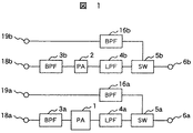
本発明の第1の実施形態を図1から図7Bを用いて説明する。図1は、2.4GHz帯の周波数帯を用いた送信多重度2のMIMOに用いる高周波回路装置の構成を示すブロック図である。本実施形態の高周波回路装置は、第一のPA1、第二のPA2、送信信号用の2個のバンドパスフィルタ3a,3b、送信信号用の2個のローパスフィルタ4a,4b、2個のスイッチ5a,5b、受信信号用の2個のバンドパスフィルタ16a,16bを含んで構成される。図では、18a,18bは送信信号の入力端子、19a,19bは受信信号の出力端子、及び6a,6bはアンテナ端子を示す。
<First Embodiment>
A first embodiment of the present invention will be described with reference to FIGS. 1 to 7B. FIG. 1 is a block diagram showing a configuration of a high-frequency circuit device used for MIMO with a transmission multiplicity of 2 using a frequency band of 2.4 GHz band. The high-frequency circuit device of this embodiment includes a first PA1, a second PA2, two band-
送信多重度2のMIMOシステムで本実施形態に示す高周波回路装置を使用して、信号を送信する場合は、第一のPA1及び第二のPA2の双方に信号が入力される。また、従来の無線LAN環境においてSISO通信を行なう場合は、第一のPA1が含まれる送信部(入力端子18a〜アンテナ端子6a)及びそれと組になっている受信部(アンテナ端子6a〜出力端子19a)のみが用いられ、第二のPA2が含まれる送信部(入力端子18b〜アンテナ端子6b)及びそれと組になっている受信部(アンテナ端子6b〜出力端子19b)は用いられない。
When a signal is transmitted using the high frequency circuit device shown in the present embodiment in a MIMO system with a transmission multiplicity of 2, the signal is input to both the first PA1 and the second PA2. When performing SISO communication in a conventional wireless LAN environment, the transmission unit (input terminal 18a to
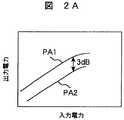
第一のPA1及び第二のPA2は、線形アンプである。これら2つのPAの入出力特性を図2Aに示す。第二のPA2は、第一のPA1よりも、線形領域において同一の入力電力に対して出力電力が約3dB小さくなるように、すなわち利得が3dB 小さくなるように設計されている。第一のPA1は、例えば送信電力の上限のみならず許容されるエラーベクトルマグニチュードの値などの無線LAN規格を満足し、かつPA出力端からアンテナまでの損失などを考慮した電力を出力するように設計されている。第一のPA1をMIMO通信に用いる場合は、第一のPA1及び第二のPA2から電力が出力されるため、第一のPA1の出力電力は約半分とする。本実施形態では第一のPA1は利得が可変であるPAを用いると良い。また本発明の第1の実施形態は、送信信号を増幅する電力増幅器に入力される信号の大きさが、SISO通信の場合も、MIMO通信の場合も同じである場合に特に適している。
The first PA1 and the second PA2 are linear amplifiers. The input / output characteristics of these two PAs are shown in FIG. 2A. The second PA2 is designed so that the output power is smaller by about 3 dB with respect to the same input power in the linear region than the first PA1, that is, the gain is smaller by 3 dB. The
図2Bは、第一のPA1及び第二のPA2の電力付加効率の出力電力依存性を示している。図2Bに示すように、同じ出力電力の場合、第二のPA2は、効率が第一のPA1の効率よりも良く、第一のPA1と同じ出力電力を出力する場合に、良い効率を保つことができる。このような効率は、第二のPA2が第一のPA1に対して最大出力電力が約3dB小さくなるように設計されているために実現される。第二のPA2として、第一のPA1と同じ入出力特性を示すPAを用いた場合は、第一,第二のPAとも効率が下がるが、本実施形態では第二のPA2の効率が良い分、全体として効率の低下が軽減される。即ち、本実施形態に示す高周波回路装置の構成とすることによって、SISO通信に対しては十分な電力を出力することができ、かつMIMO通信に対しては電力増幅器全体の効率の低下を軽減することができる。 FIG. 2B shows the output power dependence of the power added efficiency of the first PA1 and the second PA2. As shown in FIG. 2B, in the case of the same output power, the second PA2 has better efficiency than that of the first PA1, and maintains good efficiency when outputting the same output power as the first PA1. Can do. Such efficiency is achieved because the second PA2 is designed such that the maximum output power is about 3 dB less than the first PA1. When a PA having the same input / output characteristics as the first PA1 is used as the second PA2, the efficiency of both the first and second PAs is reduced. However, in this embodiment, the efficiency of the second PA2 is improved. As a whole, the decrease in efficiency is reduced. That is, with the configuration of the high-frequency circuit device shown in the present embodiment, sufficient power can be output for SISO communication, and reduction in efficiency of the entire power amplifier can be reduced for MIMO communication. be able to.
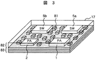
本実施形態の高周波回路装置は、図3に示すように、モジュール化して高周波モジュール17としもよい。高周波モジュール17では、多層のセラミックス基板83が用いられる。セラミックス基板83の中に、図3には示されていないが、バンドパスフィルタ3a,3b,16a,16b、ローパスフィルタ4a,4bなどが作製されている。図には示されていないが、アンテナに接続するためのアンテナ端子は、セラミックス基板83の裏面に、基板の辺に沿って設けられている。また、第一のPA1、第二のPA2及びスイッチ5a,5bは、チップ部品81と共にセラミックス基板83の表面に実装される。第一のPA1,第二のPA2やスイッチ5a,5bはベアチップ実装としても良い。更に、セラミックス基板83の上にふた82が被せられる。本実施形態では、多層のセラミックス基板83の中にフィルタ3a,3b,4a,4b,16a,16bが内蔵されるので、高周波モジュール17を小型化することができる。
As shown in FIG. 3, the high-frequency circuit device of the present embodiment may be modularized to be a high-
また、高周波モジュールの別の構造として、図4に示す高周波モジュール85がある。高周波モジュール85は、図3に示す高周波モジュール17に用いられているセラミックス基板83の実装面積を大きくして、更にセラミックアンテナ84a,84bを集積したものである。また、セラミックアンテナ84a,84bを図3に示す高周波モジュールと一体形成しても良い。
As another structure of the high frequency module, there is a
高周波モジュールの更に別の構造として、図5に示す高周波モジュール89がある。高周波モジュール89は、樹脂基板87を用いて形成される。本モジュールでは、受信用のローノイズアンプ(LNA)88a,88bやバンドパスフィルタ16a,16bなどはディスクリート部品を用いており、それらが樹脂基板87上に他の部品と共に実装される。また、樹脂基板87の中に内蔵することができる部品は、基板87上に実装せず基板に内蔵しても良いことは言うまでもない。
As still another structure of the high frequency module, there is a
また、図4に示した高周波モジュール85と同様、図6に示すように、樹脂基板87上にアンテナ90a,90bを形成し、図5に示した高周波モジュール89と一体形成することにより、アンテナも集積化した高周波モジュール91としても良い。このような高周波モジュール91を提供することにより、モジュール使用者の高周波回路設計、部品の実装という手間を省くことができる。
Further, like the
なお、図1に示した高周波回路装置は、モジュール化せずに図7Aに示すように、ディスクリート部品を用いて、例えば、マザーボードとなる基板13の上に配置することによって、構成しても良いことは言うまでもない。なお基板の形状は、その作成上、矩形であることが望ましい。図7Aの基板13の裏面を図7Bに示すが、図1で示したアンテナ用端子は、図7Bに示すように、基板13の一辺に沿って配置することが、アンテナと接続するための配線の配置を容易にするために望ましい。図7Bで端子130は第一のPA1と電気的に接続する端子、端子131は第二のPA2と電気的に接続する端子である。
The high-frequency circuit device shown in FIG. 1 may be configured by using discrete components, for example, on a
以下の実施形態において、本発明による高周波回路装置および高周波モジュールは、高周波モジュールの構成を取り上げて説明するが、そのモジュール実装及び用いられる基板などは上記と同様であるので、説明を省略する。また、第一の実施例と同様に、モジュール化せずに、ディスクリート部品をマザーボードなどの基板上に配置して、高周波回路装置を形成しても良いことは言うまでもない。 In the following embodiments, the high-frequency circuit device and the high-frequency module according to the present invention will be described by taking up the configuration of the high-frequency module. However, since the module mounting and the substrate used are the same as described above, the description thereof will be omitted. Needless to say, as in the first embodiment, a high-frequency circuit device may be formed by arranging discrete components on a substrate such as a mother board without modularization.
<第2の実施形態>
本発明の第2の実施形態を図8を用いて説明する。図8は、第1の実施形態と同様に2.4GHz帯で動作する送信多重度2のMIMO用の高周波モジュール8の回路構成を示すブロック図である。本発明の第2の実施形態は、送信信号を増幅する電力増幅器に入力される信号の大きさが、SISO通信の場合も、MIMO通信の場合も同じである場合に特に適している。本実施形態において、第一のPA1は主としてGaAs(ガリウム砒素)を用いたトランジスタを3段にカスケード接続した3段アンプであり、第二のPA2は主としてGaAsを用いたトランジスタを2段にカスケード接続した2段アンプである。第二のPA2は、トランジスタの段数を第一のPA1に比べて少なくして、全体として利得が3dB小さく、線形領域における最大出力電力が約3dB小さくなるように設計されている。
<Second Embodiment>
A second embodiment of the present invention will be described with reference to FIG. FIG. 8 is a block diagram showing a circuit configuration of a high-
第2の実施形態においても、MIMO通信のときにのみ使用されるPAが、MIMO及びSISOの両方の通信に用いられるPAよりも最大出力電力が小さくなるように構成されることにより、SISO通信に対しては十分な電力を出力することができ、かつMIMO通信に対しては、パワーアンプ全体での効率の低下を低減することが可能になる。 Also in the second embodiment, the PA used only for MIMO communication is configured so that the maximum output power is smaller than the PA used for both MIMO and SISO communication. In contrast, sufficient power can be output, and for MIMO communication, it is possible to reduce a decrease in efficiency of the entire power amplifier.
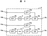
<第3の実施形態>
本発明の第3の実施形態を図9を用いて説明する。図9は、2.4GHz帯で動作する送信多重度2のMIMO用の高周波モジュール9の回路構成を示すブロック図である。本実施形態の第2の実施形態との違いは、第一のPA1は第2の実施形態と同様に主としてGaAsを用いて作製されるが、第二のPA2は主としてSi(シリコン)を用いて作製されている。第一のPA1に比べて第二のPA2は、利得を3dB小さくし、更に線形領域で最大出力電力が約3dB小さくなるように設計されている。第一のPA1と第二のPA2の使用方法と得られる効果は、これまでに述べた実施形態と同様である。本実施形態の更なる効果として、主としてSiを用いた安価なPAも用いて高周波モジュールを構成することにより第一のPA1ならびに第二のPA2の双方をGaAsを用いて高周波モジュールを構成する場合よりも高周波モジュールを低コスト化することができる。
<Third Embodiment>
A third embodiment of the present invention will be described with reference to FIG. FIG. 9 is a block diagram showing a circuit configuration of a high-
<第4の実施形態>
本発明の第4の実施形態を図10を用いて説明する。図10は、第2の実施形態と同様に2.4GHz帯で動作する送信多重度2のMIMO用の高周波モジュール10の回路構成を示すブロック図である。第一のPA1と第二のPA2は同一設計のPAであり、駆動条件が等しければ、出力電力、利得などはほぼ同一の特性を示す。本実施形態では、第一のPA1のバイアス用端子11aからバイアス電圧が供給される。また、第二のPA2のバイアス回路に、バイアス用端子11bを有するDC−DCコンバータ15が設けられ、第二のPA2にDC−DCコンバータ15から第一のPA1よりも低いバイアス電圧が供給される。本実施例では第一のPA1には約3.3V、第二のPA2には約2.3Vの電圧が供給される。このように、第二のPA2のバイアス電圧を下げると、利得はほとんど変化しないが飽和出力が低下し線形領域における最大出力電力は小さくなる。バイアス電圧をさげることで高周波モジュール10の消費電力を減らすことができる。高周波モジュール10を本実施形態に示すような構成とすることにより、モジュール全体で低消費電力化をはかることが可能となる。本実施形態に特有の効果として、第2及び第3の実施形態では種類の異なるPAが用いられたが、本実施形態では同じPAが用いられるため、MIMO用の高周波モジュール10の作製に要するPAの種類を減らすことができ、部品の調達、管理などを簡便化することができる。また、本発明の第4の実施形態は、SISO通信の場合に比べて、MIMO通信の場合はその多重度に応じて、入力電力があらかじめ小さくなっている信号の増幅に適している。
<Fourth Embodiment>
A fourth embodiment of the present invention will be described with reference to FIG. FIG. 10 is a block diagram showing a circuit configuration of a high-
<実施形態5>
本発明の第5の実施形態を図11を用いて説明する。図11は第2の実施形態と同様に2.4GHz帯で動作する送信多重度2のMIMO用の高周波モジュール12の回路構成を示すブロック図である。本実施形態の第一のPA1並びに第二のPA2はGaAs HBTによる電力増幅器である。本実施形態においては、第二のPA2の最終段のフィンガー数は第一のPAの最終段のフィンガー数の半分となっている。このように本実施形態ではトランジスタのサイズを小さくすることで第二のPA2の最大出力電力が小さくなっている。本実施形態による効果もこれまでに説明してきた実施形態と同様である。本実施形態に特有の効果として、第二のPA2のトランジスタサイズを小さくすることによって、1個のPAの作製に要するチップ面積を小さくすることができるため、結果として、高周波モジュール12を低コスト化することができる。また、第二のPA2のゲート幅を第一のPA1のゲート幅より狭くした電力増幅器を用いて構成した電力増幅器を具備してなる高周波モジュールにおいても、同様の効果が得られることは明白である。
<Embodiment 5>
A fifth embodiment of the present invention will be described with reference to FIG. FIG. 11 is a block diagram showing a circuit configuration of a high-
<第6の実施形態>
本発明の第6の実施形態を図12を用いて説明する。図12は、2.4GHz帯で動作する送信多重度3のMIMO用の高周波モジュール30の回路構成を示すブロック図である。本モジュールは、第一のPA1、第二のPA2、第三のPA32、送信信号用の3個のバンドパスフィルタ3a〜3c、送信信号用の3個のローパスフィルタ4a〜4c、受信信号用の3個のバンドパスフィルタ16a〜16c、及び3個のスイッチ5a〜5cを含んで構成される。更に、送信信号の3個の入力端子18a〜18c、受信信号の3個の出力端子19a〜19c、及び3個のアンテナ端子6a〜6cが設けられる。
<Sixth Embodiment>
A sixth embodiment of the present invention will be described with reference to FIG. FIG. 12 is a block diagram showing a circuit configuration of a high-
通信相手の受信多重度が3以上であるMIMOシステムにおいて高周波モジュール30を用いる場合、送信時には第一のPA1、第二のPA2及び第三のPA32が含まれる送信部に対して、送信信号が入力される。また、従来の無線LANシステムにおいてSISO通信を行なう場合は、送信時には第一のPA1が含まれる送信部に送信信号が入力される。また、通信相手の受信多重度が2である場合は、本実施形態では第一のPA1と第二のPA2が含まれる送信部に送信信号が入力される。
When the high-
本実施形態の高周波モジュールでは第一のPA1、第二のPA2及び第三のPA32は、主としてGaAsを用いて作製された線形アンプが用いられる。これら3個のPAの入出力特性を図13に示す。線形領域では第二のPA2は、第一のPA1よりも、同一の入力電力に対して出力電力が約3dB小さくなるように設計されたPAである。また、線形領域では第三のPA32は、第二のPA2よりも、同一の入力電力に対して約1.8dB小さくなるように設計されたPAである。第一のPA1は、従来の無線LAN規格並びにPA出力端からアンテナまでの損失などを考慮した電力を出力するように設計されたPAである。
In the high-frequency module of this embodiment, the first PA1, the second PA2, and the third PA32 are mainly linear amplifiers manufactured using GaAs. The input / output characteristics of these three PAs are shown in FIG. In the linear region, the
本実施形態においても通信相手の多重度によって使用するPA及びそこから出力される電力が変化する。送信多重度2で送信する場合は、それぞれのPAの出力電力はSISOでの出力電力よりも約3dB小さい。また、送信多重度3で送信する場合は、それぞれのPAの出力電力はSISOでの出力電力よりも約4.8dB小さい。本実施形態においては、第一のPA1はSISO通信に必要な電力が出力できるように、第二のPA2は送信多重度2の通信に必要な電力が出力できるように、第三のPA32は送信多重度3の通信に必要な電力が出力できるように、それぞれ設計されている。従って、全てが第一のPA1と同一のPAを用いてMIMO用の高周波モジュールを形成する従来の場合に比べて、PAの効率の低下を低減することができる。このように、本実施形態に示すように、送信多重度3に対応できるように構成したMIMO用の高周波モジュールにおいて、MIMO通信のときのみに使用するPAを、MIMOとSISOの双方の通信のときに用いるPAよりも最大出力電力が小さくなるように構成することにより、SISO通信に対しては十分な電力で出力でき、かつ送信多重度2及び送信多重度3のMIMO通信を行なう場合は、パワーアンプ全体での効率の低下を抑えることができ、高効率のMIMO用の高周波モジュールを提供することができる。
Also in this embodiment, the PA to be used and the power output therefrom vary depending on the multiplicity of the communication partner. When transmitting at a transmission multiplicity of 2, the output power of each PA is about 3 dB smaller than the output power in SISO. Also, when transmitting at a transmission multiplicity of 3, the output power of each PA is about 4.8 dB smaller than the output power in SISO. In this embodiment, the
次に、図14Aを用いて本実施形態の高周波モジュール31の望ましい複数のPAの配置の仕方を説明する。本実施形態で説明したPAは、SISOのときは第一のPA1、多重度が2のときは第一のPA1と第二のPA2を用いる。MIMOでは、それぞれに用いられるアンテナが相互に無相関とみなせる場合に最もMIMO効果を得ることができる。従って、アンテナの間隔は可能な限り離すことが望ましい。従って、MIMO用の高周波モジュール31を多重度2として用いる場合、図14Aに示すように、アンテナ33とアンテナ35をアンテナ34を間に挟むように配置して、通信を行なうことが望ましい。この場合、高周波モジュール31からアンテナ33、34、35までの配線を互いに交差することなしに配置するためには、多重度2の場合に用いる第一のPA1と第二のPA2を、それぞれアンテナ35、33と接続するようにし、そのためには第一のPA1並びに第二のPA2を含む送受信部がモジュールの両端に配置されることが望ましい。また、そのために第一から第三のPAがスイッチを介して、アンテナと接続するために設けられる端子の、望ましい配置を図14Bを用いて説明する。図14Bは本実施形態における高周波モジュールにおいて、PAやスイッチが搭載させる面を表面とした場合に、高周波モジュールの裏面を示した図である。アンテナと接続するための端子を、矩形のモジュールの一辺に備えており、その中で、図14Bに示した端子130、131、132が、第一から第三のPAとアンテナを接続する端子であり、端子130が第一のPA1、端子131が第二のPA2と、端子132が第三のPAとそれぞれ電気的に接続されている。本実施形態では端子130と端子131が、端子130,131,132の中で、互いの距離が最も遠くなるように配置されている。端子130,131,132をこのように配置することで、高周波モジュール内での配線を交差させることなく、高周波モジュールとアンテナとの間の配線の交差させることなく、配線を引き回すことが可能になる。
Next, a desirable arrangement of a plurality of PAs in the high-
このような構成にすることによって、図12に示した配置よりも、より高いMIMO効果を得ることが可能となる。また、高周波回路装置においても、このような端子の配置によって同様の効果を得られることは明白である。 With this configuration, it is possible to obtain a higher MIMO effect than the arrangement shown in FIG. It is obvious that the same effect can be obtained also in the high-frequency circuit device by such an arrangement of terminals.
<第7の実施形態>
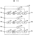
本発明の第7の実施形態を図15を用いて説明する。図15は、2.4GHz帯で動作する送信多重度3のMIMO用の高周波モジュール36の回路構成を示すブロック図である。本モジュールは、第一のPA1、2個の第二のPA2a,PA2b、送信信号用の3個のバンドパスフィルタ3a〜3c、送信信号用の3個のローパスフィルタ4a〜4c、受信信号用の3個のバンドパスフィルタ16a〜16c、及び3個のスイッチ5a〜5cを含んで構成される。本実施例では、第二のPA2aと第二のPA2bのトランジスタのサイズは略等しくなっている。
<Seventh Embodiment>
A seventh embodiment of the present invention will be described with reference to FIG. FIG. 15 is a block diagram showing a circuit configuration of a high-
また、送受信ともに多重度が3であるMIMOシステムにおいて、第一のPA1、及び2個の第二のPA2a,2bが用いられ、それらが含まれる送信部に送信信号が入力される。また、従来の無線LAN環境においてSISO通信を行なう場合は、送信時には第一のPA1が含まれる送信部のみに送信信号が入力される。本実施形態における第一のPA1はMIMO通信に用いられる場合は、SISO通信に用いられる場合に比べて、電力増幅器の増幅段数が減じられる。電力増幅器の増幅段数を変える方法は、後の実施例で説明する。
Further, in a MIMO system in which the multiplicity is 3 for both transmission and reception, the first PA1 and the two
ところで、本実施例では通信相手の受信多重度が2である場合は、先に述べた第6の実施形態とは異なり、送信時には本実施形態では第一のPA1が含まれる送信部には送信信号が入力されず、第二のPA2a,2bが含まれる2つの送信部に送信信号が入力される。すなわち、第一のPA1はOFF状態となる。第6の実施形態の場合は、多重度2で使用する場合は、第一のPA1の出力を下げて使用するためPAの効率が低下したが、本実施形態のような構成とすることにより、多重度2で使用する場合にPA全体での効率の低下を防ぐことができる。
By the way, in the present embodiment, when the reception multiplicity of the communication partner is 2, unlike the sixth embodiment described above, at the time of transmission, in the present embodiment, the transmission unit including the first PA1 transmits to the transmission unit. The signal is not input, and the transmission signal is input to the two transmission units including the
また、本実施形態では、高周波モジュールを構成するために必要となるPAの種類が、第6の実施形態よりも1種類減らせることができるので、組み立てに要するPAの種類を減らすことができ、部品の調達、管理などを簡便化することができる。 Moreover, in this embodiment, since the kind of PA required in order to comprise a high frequency module can be reduced by one kind from 6th Embodiment, the kind of PA required for an assembly can be reduced, Parts procurement and management can be simplified.
なお、多重度3で使用する場合、本実施形態の場合に、先に述べた第6の実施形態に比べて第二のPA2a,2bの一方の効率が劣化するが、第6の実施形態で用いた第三のPA32と、第7の実施形態において第三のPA32の代わりに用いる第二のPA2の出力の差は約1.8dBであるため、効率の低下を少なく済ませることができる。
In the case of use at
次に、本実施形態における望ましい複数のPAの配置の仕方について図16を用いて説明する。本実施形態では、SISOのときは第一のPA1に信号が入力され、多重度が2のときに2個の第二のPA2a,2bに信号が入力される。そのとき、図16に示すように、2個の第二のPA2a,2bを含む送受信部がモジュールの両端に配置されることが望ましい。そのような配置とすることによって、図15に示した配置よりも高いMIMO効果を得ることが可能となる。更に、図16に示す配置とした場合は、最も出力電力が大きくなる第一のPA1がモジュールの中央付近に配置されることになるため、第一のPA1による発熱をMIMO用の高周波モジュール37全体に拡散させることができる。そのため、第一のPA1からの発熱によるモジュール温度の上昇を低減することが可能になる。
Next, a desirable way of arranging a plurality of PAs in this embodiment will be described with reference to FIG. In this embodiment, a signal is input to the first PA1 when SISO is used, and a signal is input to the two
なお、図16に示す配置とした場合の高周波モジュールの例を図17Aに示す。高周波モジュール80のセラミックス基板83の中に、図17Aには示されていないが、バンドパスフィルタ3a,3b,3c,16a,16b,16c、ローパスフィルタ4a,4b,4cなどが作製されている。基板83の表面の中央に第一のPA1及びスイッチ5bが実装され、同表面の両側に第二のPA2aとスイッチ5a及び第二のPA2bとスイッチ5cがそれぞれ実装されている。チップ部品81もこれらと共に同表面に実装される。また、セラミックス基板83の上にふた82が被せられる。本実施形態における第一から第三のPAがスイッチを介して、アンテナと接続するために設けられる端子の、望ましい配置を図17Bを用いて説明する。図17Bは図17Aに示した高周波モジュールの裏面を示した図である。アンテナと接続するための端子を、矩形のモジュールの一辺に備えており、その中で、図17Bに示した端子130、131、132が、第一のPA1、第二のPA2a、第二のPA2bとアンテナを接続する端子であり、端子130が第一のPA1、端子131が第二のPA2bと、端子132が第二のPA2aとそれぞれ電気的に接続されている。このように配置することで、高周波モジュール内での配線を交差させることなく、高周波モジュールとアンテナとの間の配線の交差させることなく、配線を引き回すことが可能になる。本実施形態では、最大の出力電力を有する第一のPA1と電気的に接続される端子130が、第二のPA2a並びに第二のPA2bと電気的に接続される端子の間になるように配置されている。高周波回路装置においても、このような端子の配置によって同様の効果を得られる。
FIG. 17A shows an example of a high-frequency module in the case of the arrangement shown in FIG. Although not shown in FIG. 17A, band-
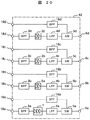
<第8の実施形態>
本発明の第8の実施形態を図18を用いて説明する。図18は、2.4GHz帯で動作する送信多重度4のMIMO用の高周波モジュール40の回路構成を示すブロック図である。本モジュールは、第一のPA1、第二のPA2、第三のPA32、第四のPA41、送信信号用の4個のバンドパスフィルタ3a〜3d、送信信号用の4個のローパスフィルタ4a〜4d、受信信号用の4個のバンドパスフィルタ16a〜16d、並びに4個のスイッチ5a〜5dを含んで構成される。更に、送信信号の4個の入力端子18a〜18d、受信信号の4個の出力端子19a〜19d、及び4個のアンテナ端子6a〜6dが設けられる。
<Eighth Embodiment>
An eighth embodiment of the present invention will be described with reference to FIG. FIG. 18 is a block diagram showing a circuit configuration of a high-
多重度が4であるMIMOシステムにおいて、第一のPA1、第二のPA2、第三のPA32及び第四のPA41に送信信号が入力される。また、従来の無線LAN環境においてSISO通信を行なう場合は、送信時には第一のPA1が含まれる送信部のみに送信信号が入力される。また、通信相手の受信多重度が2である場合は、送信時には本実施形態では第一のPA1及び第二のPA2が含まれる送信部のみに送信信号が入力される。また、通信相手の受信多重度が3である場合は、送信時には本実施形態では第一のPA1、第二のPA2及び第三のPA32が含まれる送信部のみに送信信号が入力される。これら4個のPAは、主としてGaAsを用いて作製された線形アンプである。これら4個のPAの入出力特性を図19に示す。線形領域では第二のPA2は、第一のPA1よりも、同一の入力電力に対して出力電力が約3dB小さくなるように設計されている。また、第三のPA32は、第二のPA2よりも、同一の入力電力に対して約1.8dB小さくなるように設計されている。また更に、第四のPA41は、第三のPA32よりも、同一の入力電力に対して約1.2dB小さくなるように設計されている。第一のPA1は、従来の無線LAN規格並びにPA出力端からアンテナまでの損失などを考慮した電力を出力するように設計されている。
In a MIMO system with a multiplicity of 4, a transmission signal is input to the first PA1, the second PA2, the third PA32, and the fourth PA41. When performing SISO communication in a conventional wireless LAN environment, a transmission signal is input only to the transmission unit including the first PA1 during transmission. Further, when the reception multiplicity of the communication partner is 2, at the time of transmission, in this embodiment, the transmission signal is input only to the transmission unit including the first PA1 and the second PA2. Further, when the reception multiplicity of the communication partner is 3, at the time of transmission, in this embodiment, the transmission signal is input only to the transmission unit including the first PA1, the second PA2, and the third PA32. These four PAs are linear amplifiers made mainly using GaAs. The input / output characteristics of these four PAs are shown in FIG. In the linear region, the
本実施形態により、これまでに説明した多重度2、又は多重度3のMIMOと同様の効果が得られることは明白である。
It is apparent that the present embodiment can provide the same effect as the
<第9の実施形態>
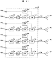
本発明の第9の実施形態を図20を用いて説明する。図20は、2.4GHz帯で動作する送信多重度4のMIMO用の高周波モジュール42の回路構成を示すブロック図である。本モジュールは、第一のPA1、3個の第二のPA2a〜2c、送信信号用の4個のバンドパスフィルタ3a〜3d、送信信号用の4個のローパスフィルタ4a〜4d、受信信号用の4個のバンドパスフィルタ16a〜16d、及び4個のスイッチ5a〜5dを含んで構成される。更に、送信信号の4個の入力端子18a〜18d、受信信号の4個の出力端子19a〜19d、及び4個のアンテナ端子6a〜6dが設けられる。
<Ninth Embodiment>
A ninth embodiment of the present invention will be described with reference to FIG. FIG. 20 is a block diagram showing a circuit configuration of a high-
本実施形態では、送受信端末ともに多重度が4であるMIMOシステムにおいて、第一のPA1及び3個の第二のPA2a〜2cが含まれる送信部に信号が入力される。また、従来の無線LAN環境においてSISO通信を行なう場合は、送信時には第一のPA1が含まれる送信部のみに送信信号が入力される。
In the present embodiment, in a MIMO system in which the multiplicity is 4 for both transmission and reception terminals, signals are input to a transmission unit including the first PA1 and the three
一方、通信相手の受信多重度が2である場合は、先に述べた実施形態とは異なり、送信時には本実施形態では第一のPA1が含まれる送信部は使用されず、3個のうちの2個の第二のPA2が用いられ、同2個の第二のPA2が含まれる2個の送信部に送信信号が入力される。また、通信相手の受信多重度が3である場合は、送信時には第一のPA1が含まれる送信部は使用されずに、3個の第二のPA2が含まれる3個の送信部に送信信号が入力される。このような構成とすることで、本発明の第7の実施形態と同様の効果を得ることができる。また、図21に示すように、2個の第二のPA2a,2cを含む送受信部がモジュール43の両端に配置され、最も出力電力が大きくなる第一のPA1が2個の第二のPA2a,2cの中間に配置されることが望ましい。第8の実施形態の場合と同様に、より高いMIMO効果と発熱低減の効果を得ることができる。
On the other hand, when the reception multiplicity of the communication partner is 2, unlike the embodiment described above, the transmission unit including the first PA1 is not used in the present embodiment at the time of transmission. Two second PA2 are used, and a transmission signal is input to two transmission units including the two second PA2. Also, when the reception multiplicity of the communication partner is 3, the transmission unit including the first PA1 is not used at the time of transmission, and the transmission signal is transmitted to the three transmission units including the three second PA2. Is entered. By adopting such a configuration, it is possible to obtain the same effect as that of the seventh embodiment of the present invention. In addition, as shown in FIG. 21, transmission / reception units including two
<第10の実施形態>
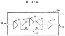
本発明の第10の実施形態を図22から図25を用いて説明する。第1〜第9の実施形態において、MIMO用とSISO用の両方に用いられるPAのMIMO通信時の効率、及びMIMO用に用いられても、通信相手の多重度によって予め設計された最適な出力電力よりも小さい電力を出力する場合があるPAの小さい電力を出力する時の効率は、予め設計された最適な出力電力のときの効率よりも低い。本実施形態で用いられるPAは、PAの内部のトランジスタの接続を予め設計された最適な出力電力で出力する時と小さい電力を出力する時とで切り替えることにより、小さい電力を出力する時でも高い効率が得られるように構成される。本実施形態では、高周波モジュールの回路構成の説明は省略し、PAの構成についてのみ説明することとする。
<Tenth Embodiment>
A tenth embodiment of the present invention will be described with reference to FIGS. In the first to ninth embodiments, the optimal output designed in advance according to the efficiency of the MIMO communication of the PA used for both MIMO and SISO and the multiplicity of the communication partner even if used for MIMO The efficiency at the time of outputting the small power of the PA that may output the power smaller than the power is lower than the efficiency at the time of the optimal output power designed in advance. The PA used in the present embodiment is high even when outputting small power by switching the connection of the transistors inside the PA between when outputting at the optimal output power designed in advance and when outputting low power. Configured for efficiency. In the present embodiment, description of the circuit configuration of the high-frequency module is omitted, and only the configuration of the PA is described.
本実施形態によるPA20は、図22に示すようにトランジスタを3段にカスケード接続した、すなわち一段目21、二段目22及び3段目23から構成された3段アンプである。図22に示したPA20では、2段目22と3段目23の間、及び三段目23と出力端子6の間に、それぞれスイッチ24とスイッチ25が設けられている。本実施例ではPA20は、例えば、PA20の全利得を25dBとし、これら3段のゲイン配分が順に10:9:6となるように設計される。PA20を本実施形態の構成とすることにより、例えばSISO通信の場合は、3段全部用いて信号を増幅し、また、多重度4のMIMO通信に用いる場合は、スイッチ24とスイッチ25によって3段目を切り離すことによって、6dB利得が小さいPAを構成することができる。
The
図22に示したPA20では、2個のスイッチが使用されるが、図23や図24Aに示すように1個のスイッチ24又はスイッチ25のみを含んでPAを構成することが可能である。図23に示すように2段目22と3段目23の間にスイッチ24を設ける場合は、3段目23の出力に高周波線路26が付加されていることを考慮した整合回路の設計が必要になる。図24Aに示す構成の場合は、段間に高周波線路26が付加されることを考慮した整合回路の設計が必要になる。図22から図24Aに示すPAでは、3段目のトランジスタを切りはなす構成となっているが、図24Bに示すように初段のトランジスタを切りはなす、または図24Cに示すように2段目のトランジスタを切りはなす構成としても良いことは言うまでもない。
In the
また、図25に示すPAでは、通信相手の多重度によって出力電力が変化するPA28のバイアス回路にDC−DCコンバータ27が設けられる。DC−DCコンバータ27によって、通信相手の多重度によってPA28のバイアス電圧が変更される。それにより、小さい電力を出力する時にPA28の消費電力を低減することが可能になる。
In the PA shown in FIG. 25, a DC-
<第11の実施形態>
本発明の第11の実施形態を図26Aを用いて説明する。図26Aは2.4GHz帯で動作する送信多重度4のMIMO用の高周波モジュール50の回路構成を示すブロック図である。本モジュールは、第一のPA1、3個の第二のPA2a〜2c、送信信号用の4個のバンドパスフィルタ3a〜3d、送信信号用の4個のローパスフィルタ4a〜4d、4個のスイッチ5a〜5d、さらに4個のスイッチ53a〜53dを含んで構成される。本実施形態のモジュールは、図20を用いて説明した第9の実施形態と同様に使用することができるが、本実施形態と第9の実施形態との差は、本実施形態の高周波モジュールには、PAが電気的に接続するアンテナを切り替える4個のスイッチ53a〜53dが備えられる点にある。
<Eleventh embodiment>
An eleventh embodiment of the present invention will be described with reference to FIG. 26A. FIG. 26A is a block diagram showing a circuit configuration of a high-
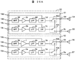
本実施形態における高周波回路モジュールを用いた無線通信機の機能ブロック図を図26Bに示す。本実施形態を用いて構成した無線通信機では、トレーニングパケット生成部147により、例えば、通信相手となる無線通信機に対して、自身の多重度や通信可能な変調方式など通信相手の無線通信機との通信に必要な情報を送信する。また、相手の無線通信機からの同様の情報をトレーニングパケット受信部146で受信し、ビットエラーレートを測定する。通信相手となる無線通信機とこのようなやり取りを相互に行ない、通信相手の多重度を判定し、無線通信機との最適な通信方法を、MIMO制御部145が総合的に判断する。その結果をもとに、MIMO制御部145は、制御信号150を用いて、送信RF制御144、受信RF制御143、送信RF部142、受信RF部141の制御を行ない、自身の多重度を制御する。このトレーニングパケットの送受信は定期的に行なわれるが、無線通信機に電源が投入されてから最初に行なわれるトレーニングパケットの送受信はSISO通信により行なわれる。それ以降は、SISO通信または前回パケットを送った時の通信方式を用いて行なわれる。
FIG. 26B shows a functional block diagram of a wireless communication device using the high-frequency circuit module in the present embodiment. In the wireless communication device configured using the present embodiment, the training
本実施形態に示す高周波モジュール50を用いて構成した無線通信機が通信する相手の受信多重度が2である場合は、本実施形態に示す高周波モジュール50を用いて構成した無線通信機の送信多重度を2にする必要がある。そのとき、高周波モジュール50に具備されている4個の送受信部を図26Aに示すように、構成要素部分51と構成要素部分52の2つの組に分けて用いる。このとき構成要素部分51側には、スイッチ53d、53cが、構成要素52側にはスイッチ53a,53bが具備される。
When the reception multiplicity of the partner with which the wireless communication device configured using the high-
高周波モジュール50をこのように構成することにより、相手の無線通信機の受信多重度が2である場合は、本実施形態の高周波モジュールでは、第二のPA2aと第二のPA2bの電力増幅器に送信信号が入力される。そして、第二のPA2aからの信号がアンテナ56又はアンテナ57のいずれかから送信されるようにスイッチ53a,53bが切り替えられる。また、第二のPA2bからの信号はアンテナ54又はアンテナ55のいずれかから送信されるようにスイッチ53c,53dが切り替えられる。これらのスイッチ53a,53b、53c,53dの切り替え制御は、MIMO制御部145がスイッチ部140に送る制御信号150によって、制御される。定期的に行なわれるトレーニングパケットの送受信のビットエラーレート、または、通常のデータ伝送におけるビットエラーレートが、あらかじめ設定された閾値以上になった場合に、スイッチ53a,53b、53c,53dを切り替える。スイッチ53a,53b、53c,53dを切り替えることによって、ビットエラーレートがさらに悪くならなければ、スイッチ53a,53b、53c,53dを切り替えた状態で、すなわち通信に使用するアンテナを変更した状態で通信を行なう。このように、スイッチ53a,53b、53c,53dを切り替えることにより、より良い伝搬条件で通信を行なうことができる送信ダイバシティが実現される。本実施形態の高周波モジュールには受信部も含まれているため、受信ダイバシティを実現することもできる。このように本実施形態の高周波モジュールは第二のPA2a並びに第二のPA2bが電気的に接続するアンテナを切り替えるためのスイッチを具備して構成されており、その結果として、より良い通信条件で相手の無線通信機と通信することができる。本実施形態では、高周波モジュールの形態で説明したが、モジュール化していない高周波回路装置でも同様である。本実施形態の場合は、通信相手の受信多重度が2以外でも、4未満であれば同様の効果を得ることができる。
By configuring the high-
図26Aの実施形態では、アンテナのみを切り替えたアンテナダイバシティが実現されるが、図27に示すようにMIMO用の高周波モジュール58の全ての送信部を用いて送信ダイバシティ効果を得ることもできる。この場合は、例えば、図26Bに示すMIMO制御部145からの制御信号150を送信RF制御部が受けて、相互に符号が異なるデータをアンテナ54〜57から送信することにより、ダイバシティ効果が実現される。
In the embodiment of FIG. 26A, antenna diversity with only the antenna switched is realized. However, as shown in FIG. 27, the transmission diversity effect can also be obtained by using all the transmission units of the
<第12の実施形態>
本発明の第12の実施形態を図28を用いて説明する。図28は、送信多重度2のMIMO用の高周波モジュール60の回路構成を示すブロック図である。本モジュールは、3個の第一のPA1a〜1c、3個の第二のPA2a〜2c、送信信号用の6個のバンドパスフィルタ3a〜3f、送信信号用の6個のローパスフィルタ4a〜4f、6個のスイッチ5a〜5f、更に受信信号用の6個のバンドパスフィルタ16a〜16fを含んで構成される。
<Twelfth Embodiment>
A twelfth embodiment of the present invention will be described with reference to FIG. FIG. 28 is a block diagram showing a circuit configuration of a high-
本実施形態では、使用するPAの種類によって、MIMO用の高周波モジュールの構成要素部分61、及びMIMO用の高周波モジュールの構成要素部分62の2つの組に分け、それぞれの組の中で、アンテナのビーム形状を設定する、即ちビームフォーミングを行なうことができる構成となっている。アンテナビームフォーミングにより、より良い通信状態で通信を行なうことが可能になる。本実施形態を用いた無線通信機の機能ブロックは図26Bと略同様であるため、図26Bを用いて説明するが、MIMO制御部145からの制御信号150により送信RF制御部が、それぞれの送信部に入力される送信信号の振幅と位相を決定し、アンテナビームフォーミングを行なう。
In the present embodiment, depending on the type of PA to be used, it is divided into two groups, that is, a
<第13の実施形態>
本発明の第13の実施形態を図29を用いて説明する。図29は、デュアルバンド対応の送信多重度2のMIMO用の高周波モジュール107の回路構成を示すブロック図である。本実施形態では、2.4GHz帯用のMIMO用の高周波モジュール7と5GHz帯用のMIMO用の高周波モジュール108とを組み合わせて高周波モジュール107が構成される。このような構成の高周波モジュール107を用いることにより、デュアルバンドのMIMOに対応する無線LANカードを容易に実現することができる。
<13th Embodiment>
A thirteenth embodiment of the present invention will be described with reference to FIG. FIG. 29 is a block diagram showing a circuit configuration of the high-
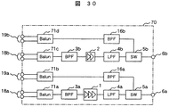
以上、本発明の高周波回路装置及び高周波モジュールの実施形態を述べたが、各実施形態における回路構成は、本発明の趣旨を逸脱しない範囲で、今までに述べたものに限らないことは言うまでもない。例えば、図30に示すMIMO用の高周波モジュール70は、第2の実施形態などにおいて説明したMIMO用の高周波モジュールに、更に送信経路並びに受信経路にバラン(Balun)71a,71b,71c,71dを設けた構成となっている。また、図31に示すMIMO用の高周波モジュール72は、第1の実施形態で説明した高周波モジュール17に対して、バンドパスフィルタを除いた構成となっている。また、図32に示すMIMO用の高周波モジュール73は、第一のPA1、第二のPA2及びそれらの入力整合回路(I−M)74a,74bと出力整合回路(O−M)75a,75bからのみ構成されている。
Although the embodiments of the high-frequency circuit device and the high-frequency module of the present invention have been described above, it is needless to say that the circuit configuration in each embodiment is not limited to the above-described ones without departing from the gist of the present invention. . For example, the high-
また送信部のみによる高周波回路装置および高周波モジュールであっても、本発明の効果を得られることは明白である。また本発明の高周波回路装置および高周波モジュールは、RF−ICやベースバンド部の機能を有するように構成しても良いことは言うまでもない。また、周波数帯域も本実施例で述べた周波数帯に限ったものではなく、本発明の趣旨を逸脱しなければ、他の周波数帯でも同様の効果を得られることは明白である。 In addition, it is obvious that the effects of the present invention can be obtained even with a high-frequency circuit device and a high-frequency module using only a transmitter. Needless to say, the high-frequency circuit device and the high-frequency module of the present invention may be configured to have functions of an RF-IC and a baseband unit. Further, the frequency band is not limited to the frequency band described in this embodiment, and it is obvious that the same effect can be obtained in other frequency bands without departing from the gist of the present invention.
また、PAに用いる主な材料は、GaAsやSiに限るものではなく、SiGe、InGaPなどでも良い。また、PAは、幾つかのプロセスが混在して形成されても良く、またその構造も特定のものに限ったものではなく、信号を増幅する機能を有するものであれば良いことは言うまでもない。 The main material used for PA is not limited to GaAs or Si, but may be SiGe, InGaP, or the like. Further, the PA may be formed by mixing several processes, and the structure is not limited to a specific one, and it is needless to say that the PA has a function of amplifying a signal.
更に、送受信の多重度、PAの種類、利得、複数個設けたPAのそれぞれの出力電力の関係などは、本実施形態に述べたものに限るものでないことは明白であり、本発明の趣旨を逸脱しない範囲であれば用途に適した値を用いれば良いことは言うまでもない。 Furthermore, it is clear that the multiplicity of transmission / reception, the type of PA, the gain, and the relationship between the output powers of each of the plurality of PAs are not limited to those described in the present embodiment, and the gist of the present invention It goes without saying that a value suitable for the application may be used as long as it does not deviate.
<第14の実施形態>
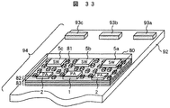
本発明の第14の実施形態を図33を用いて説明する。図33は、セラミックス基板83を用いて作製した高周波モジュール80を含んで構成した無線LANモジュール94である。マザーボードとなる樹脂基板92上に高周波モジュール80とセラミックで作製したアンテナ93a,93b,93cを実装している。本発明による高周波モジュール80に上記の本発明の高周波モジュール(例えば、図16に示した高周波モジュール37)を用いることにより、電力増幅器の効率の低下が低減された無線LANモジュールを実現することができる。
<Fourteenth embodiment>
A fourteenth embodiment of the present invention will be described with reference to FIG. FIG. 33 shows a
なお、これらの無線LANモジュールではセラミックアンテナが用いられているが、所望の周波数の電波を送受信できるのであれば、どのようなアンテナでも良いことは明らかである。 These wireless LAN modules use ceramic antennas, but it is obvious that any antenna can be used as long as it can transmit and receive radio waves of a desired frequency.
1,1a,1b,1c…第一のパワーアンプ、2,2a,2b,2c…第二のパワーアンプ、3a,3b,3c,3d,3e,3f,16a,16b,16c,16d,16e,16f…バンドパスフィルタ、4a,4b,4c,4d,4e,4f…ローパスフィルタ、5a,5b,5c,5d,5e,5f…スイッチ、6a,6b,6c,6d…アンテナ端子、8,9,10,12,17,80,85,89,91…高周波モジュール、11…バイアス用端子、13…基板、15…DC−DCコンバータ、18a,18b,18c,18d…入力端子、19a,19b,19c,19d…出力端子、81…チップ部品、82,86…ふた、83…セラミックス基板、84a,84b,93a,93b,93c…セラミックアンテナ、87,92…樹脂基板、88…ローノイズアンプ、90a,90b…アンテナ、94…無線LANモジュール、20,28…通信相手の多重度によって出力電力がかわるパワーアンプ、21…パワーアンプ20の一段目、22…パワーアンプ20の二段目、23…パワーアンプ20の三段目、24,25…スイッチ、26…高周波線路、27…DC−DCコンバータ、30,31,36,37…高周波モジュール、33,34,35…アンテナ、32…第三のパワーアンプ、40,42,43…高周波モジュール、41…第四のパワーアンプ、44,45,46,47…アンテナ、50,58…高周波モジュール、51,52…構成要素部分、53…スイッチ、54,55,56,57…アンテナ、60…高周波モジュール、61,62…構成要素部分、63,64…アンテナ、67…出力端子、70,72,73…高周波モジュール、71a,71b,71c,71d…バラン、74a,74b…パワーアンプの入力整合回路、75a,75b…パワーアンプの出力整合回路、80,85,89,91…高周波モジュール、101…第五のパワーアンプ、102…第六のパワーアンプ、103…バンドパスフィルタ、104…ローパスフィルタ、105…スイッチ、106…高周波信号用端子、107…高周波モジュール、108…高周波モジュール、111…パワーアンプ、113…バンドパスフィルタ、114…ローパスフィルタ、115…スイッチ、116…バラン、117a,117b…アンテナ、118…RFIC、120…回路部分、130,131,132…端子、140…スイッチ部、141…受信RF部、142…送信RF部、143…受信RF制御、144…送信RF制御、145…MIMO制御部、146…トレーニングパケット受信部、147…トレーニングパケット送信部、148…スイッチ、149…スイッチ、150…制御信号。
1, 1a, 1b, 1c ... first power amplifier, 2, 2a, 2b, 2c ... second power amplifier, 3a, 3b, 3c, 3d, 3e, 3f, 16a, 16b, 16c, 16d, 16e, 16f: Band pass filter, 4a, 4b, 4c, 4d, 4e, 4f ... Low pass filter, 5a, 5b, 5c, 5d, 5e, 5f ... Switch, 6a, 6b, 6c, 6d ... Antenna terminal, 8, 9, 10, 12, 17, 80, 85, 89, 91 ... high frequency module, 11 ... bias terminal, 13 ... substrate, 15 ... DC-DC converter, 18a, 18b, 18c, 18d ... input terminal, 19a, 19b, 19c , 19d: output terminal, 81: chip component, 82, 86: lid, 83: ceramic substrate, 84a, 84b, 93a, 93b, 93c ... ceramic antenna, 87, DESCRIPTION OF
Claims (16)
上記複数の電力増幅器は、相互に最大出力電力が異なる少なくとも2個の電力増幅器を含む、3個以上の電力増幅器であり、
MIMO(Multiple Input Multiple Output)通信方式で用いられる電力増幅器の数がSISO(Single Input Single Output)通信方式で用いられる電力増幅器の数よりも大きく、
上記高周波モジュールは更に、複数のアンテナと上記複数の電力増幅器とを1対1に対応させて電気的に接続するための複数の端子を具備してなり、
上記複数の電力増幅器は上記複数の端子とそれぞれ電気的に接続され、
上記高周波モジュールは更に、平面図が4辺を有する矩形形状となるような基板を具備してなり、
上記複数の端子は共に上記基板の裏面の上記4辺のうちの1辺に沿って配置され、上記複数の電力増幅器は配線を交差させることなく上記複数の端子とそれぞれ電気的に接続されており、
上記高周波回路装置がMIMO通信方式で動作する場合、1つの送信信号に対して上記複数の電力増幅器のうちの少なくとも2つの電力増幅器が用いられ、該MIMO通信方式で動作する電力増幅器は、上記複数の端子のうち端子間の平均距離が最大となるように選択された少なくとも2つの端子にそれぞれ電気的に接続されている
ことを特徴とする高周波モジュール。 Comprising a plurality of power amplifiers for amplifying transmission signals;
It said plurality of power amplifiers are mutually maximum output power is different at least two including a power amplifier, a three or more power amplifiers,
The number of power amplifiers used in MIMO (Multiple Input Multiple Output) communication system is larger than the number of power amplifiers used in SISO (Single Input Single Output) communication system,
The high-frequency module further includes a plurality of terminals for electrically connecting the plurality of antennas and the plurality of power amplifiers in a one-to-one correspondence.
The plurality of power amplifiers are electrically connected to the plurality of terminals, respectively.
The high frequency module further comprises a substrate whose plan view is a rectangular shape having four sides,
Each of the plurality of terminals is disposed along one of the four sides on the back surface of the substrate, and the plurality of power amplifiers are electrically connected to the plurality of terminals without crossing wirings. ,
When the high-frequency circuit device operates in the MIMO communication system, at least two of the plurality of power amplifiers are used for one transmission signal, and the power amplifier operating in the MIMO communication system includes the plurality of power amplifiers. A high-frequency module characterized in that each of the terminals is electrically connected to at least two terminals selected so as to maximize the average distance between the terminals .
上記複数の端子のうち上記基板の上記1辺の両端に最も近い2つの端子にそれぞれ電気的に接続された上記2つの電力増幅器以外の電力増幅器のうちの少なくとも1つは、上記2つの電力増幅器よりも前記最大出力電力が大きい
ことを特徴とする高周波モジュール。 In claim 1,
Among the plurality of terminals, at least one of the power amplifiers other than the two power amplifiers electrically connected to two terminals closest to both ends of the one side of the substrate is the two power amplifiers. The high-frequency module characterized in that the maximum output power is larger than that .
上記高周波モジュールがMIMO通信方式で動作する場合に用いられる前記電力増幅器の任意の2つの電力増幅器の前記最大出力電力が互いにほぼ等しく、
上記高周波モジュールは、周波数帯域が異なる2つのMIMO通信方式の少なくともいずれかで動作するように構成されている
ことを特徴とする高周波モジュール。 In claim 1,
The maximum output power of any two power amplifiers of the power amplifier used when the high-frequency module operates in a MIMO communication system is substantially equal to each other;
The high-frequency module is configured to operate in at least one of two MIMO communication systems having different frequency bands .
上記高周波モジュールは、少なくとも、送受信信号に作用するフィルタ、送受切替用のスイッチ、上記複数のアンテナ、上記複数の増幅器の入出力側に接続した入力整合回路及び出力整合回路、送受信経路に挿入したバランのいずれかを含んで構成されている
ことを特徴とする高周波モジュール。 In claim 1,
The high-frequency module includes at least a filter acting on a transmission / reception signal, a switch for transmission / reception switching, the plurality of antennas, an input matching circuit and an output matching circuit connected to input / output sides of the plurality of amplifiers, and a balun inserted in the transmission / reception path. A high-frequency module comprising any of the above .
上記複数の電力増幅器は、相互に最大出力電力が異なる少なくとも2個の電力増幅器を含む、3個以上の電力増幅器であり、
上記高周波モジュールは更に、平面図が4辺を有する矩形形状となるような基板を具備してなり、
複数のアンテナと上記複数の電力増幅器とを1対1に対応させて電気的に接続するための複数の端子を具備してなり、
上記複数の電力増幅器は上記複数の端子とそれぞれ電気的に接続され、
上記複数の端子は共に上記基板の裏面の上記4辺のうちの1辺に沿って配置され、上記複数の電力増幅器は配線を交差させることなく上記複数の端子とそれぞれ電気的に接続されており、
上記高周波回路装置がMIMO通信方式で動作する場合、1つの送信信号に対して上記複数の電力増幅器のうちの少なくとも2つの電力増幅器が用いられ、該MIMO通信方式で動作する電力増幅器は、互いに最大出力電力がほぼ等しい
ことを特徴とする高周波モジュール。 A plurality of power amplifiers for amplifying transmission signals having at least a part of the frequency band being equal;
The plurality of power amplifiers are three or more power amplifiers including at least two power amplifiers having different maximum output powers from each other,
The high frequency module further comprises a substrate whose plan view is a rectangular shape having four sides,
A plurality of terminals for electrically connecting a plurality of antennas and the plurality of power amplifiers in a one-to-one correspondence;
The plurality of power amplifiers are electrically connected to the plurality of terminals, respectively.
Each of the plurality of terminals is disposed along one of the four sides on the back surface of the substrate, and the plurality of power amplifiers are electrically connected to the plurality of terminals without crossing wirings. ,
When the high frequency circuit device operates in the MIMO communication system, at least two power amplifiers of the plurality of power amplifiers are used for one transmission signal, and the power amplifiers operating in the MIMO communication system are mutually maximum. A high-frequency module characterized in that output power is substantially equal .
上記高周波モジュールは相互に最大出力電力が異なる2種類の電力増幅器を具備してなり、上記最大出力電力が他より大きい電力増幅器は、上記最大出力電力が他より小さく上記MIMO通信方式で動作する電力増幅器がそれぞれ接続される上記端子の間に配置されている端子に接続される
ことを特徴とする高周波モジュール。 In claim 5,
The high-frequency module includes two types of power amplifiers having different maximum output powers, and the power amplifier having a maximum output power larger than the other is a power that operates with the MIMO communication method with the maximum output power being smaller than the others. A high-frequency module, wherein the amplifier is connected to a terminal disposed between the terminals to which the amplifier is connected .
上記電力増幅器と1対1に対応させて電気的に接続するアンテナを切り替えるためのスイッチを具備してなる
ことを特徴とする高周波モジュール。 In claim 5 ,
A high-frequency module comprising a switch for switching an antenna electrically connected to the power amplifier in a one-to-one correspondence .
上記高周波モジュールは、少なくとも、送受信信号に作用するフィルタ、送受切替用のスイッチ、上記複数のアンテナ、上記複数の電力増幅器の入出力側に接続した入力整合回路及び出力整合回路、送受信経路に挿入したバランのいずれかを含んで構成されている
ことを特徴とする高周波モジュール。 In claim 5 ,
The high-frequency module includes at least a filter acting on a transmission / reception signal, a switch for transmission / reception switching, the plurality of antennas, an input matching circuit and an output matching circuit connected to input / output sides of the plurality of power amplifiers, and a transmission / reception path A high-frequency module comprising one of baluns .
上記最大出力電力が異なる2種類の電力増幅器として、第1の電力増幅器、及び、第2の電力増幅器を具備して成り、
前記第1の電力増幅器は前記SISO通信に必要な電力が出力できるように構成され、前記第2の電力増幅器第2のPA2は送信多重度2の通信に必要な電力が出力できるように構成され、
上記第1の電力増幅器は、GaAsトランジスタを3段にカスケード接続した3段増幅器であり、上記第2の電力増幅器は、上記第1の電力増幅器よりもカスケード接続段数が少ない増幅器である
ことを特徴とする高周波モジュール。 In claim 6,
The two types of power amplifiers having different maximum output powers include a first power amplifier and a second power amplifier ,
The first power amplifier is configured to output power necessary for the SISO communication, and the second power amplifier second PA2 is configured to output power necessary for transmission multiplicity 2 communication. ,
The first power amplifier is a three-stage amplifier in which GaAs transistors are cascade-connected in three stages, and the second power amplifier is an amplifier having a smaller number of cascade connection stages than the first power amplifier. > A high-frequency module characterized by
上記基板は、多層のセラミック基板又は樹脂基板のいずれかである
ことを特徴とする高周波モジュール。 In claim 5 ,
The high-frequency module according to claim 1, wherein the substrate is a multilayer ceramic substrate or a resin substrate .
上記基板は、多層のセラミック基板であり、上記多層のセラミック基板の中に送受信号に作用するフィルタが内蔵されており、
上記基板は、セラミックアンテナを集積している
ことを特徴とする高周波モジュール。 In claim 10 ,
The substrate is a multilayer ceramic substrate, and a filter acting on a transmission / reception signal is built in the multilayer ceramic substrate,
The high-frequency module , wherein the substrate is integrated with a ceramic antenna .
上記最大出力電力が異なる2種類の電力増幅器として、第1の電力増幅器、第2の電力増幅器、及び、第3の電力増幅器を具備して成り、
前記第1の電力増幅器は前記SISO通信に必要な電力が出力できるように構成され、前記第2の電力増幅器第2のPA2は送信多重度2の通信に必要な電力が出力できるように構成され、前記第3の電力増幅器は送信多重度3の通信に必要な電力が出力できるように構成されている
ことを特徴とする高周波モジュール。 In claim 6,
The two types of power amplifiers having different maximum output powers include a first power amplifier, a second power amplifier, and a third power amplifier ,
The first power amplifier is configured to output power necessary for the SISO communication, and the second power amplifier second PA2 is configured to output power necessary for transmission multiplicity 2 communication. The high-frequency module , wherein the third power amplifier is configured to output power necessary for transmission multiplicity 3 communication .
上記複数の端子として、上記第1の電力増幅器に電気的に接続される第1の端子と上記第2の電力増幅器に電気的に接続される第2の端子と上記第3の電力増幅器に電気的に接続される第3の端子とを有し、
上記第1の端子と上記第2の端子とが、上記第1の端子と上記第2の端子と上記第3の端子の中で、互いに距離が最も遠く配置されている
ことを特徴とする高周波モジュール。 In claim 12,
The plurality of terminals are electrically connected to a first terminal electrically connected to the first power amplifier, a second terminal electrically connected to the second power amplifier, and the third power amplifier. And a third terminal connected to each other,
The first terminal and the second terminal are disposed farthest from each other among the first terminal, the second terminal, and the third terminal. High-frequency module featuring
上記最大出力電力が異なる2種類の電力増幅器として、相互に最大出力電力が異なる第1の電力増幅器と2個の第2aと第2bの電力増幅器とを有し、
上記2個の第2aと第2bの電力増幅器は、増幅器を構成するトランジスタの前記最大出力電力が略等しく、上記第1の電力増幅器の出力の最大値が上記第2aと第2bの電力増幅器のそれぞれの出力の最大値よりも大きく、
上記複数の端子として、上記第1の電力増幅器に電気的に接続される第1の端子と上記第2aの電力増幅器に電気的に接続される第2aの端子と上記第2bの電力増幅器に電気的に接続される第2bの端子とを有し、
上記第1の端子が上記第2aの端子と上記第2bの端子との間に配置されている
ことを特徴とする高周波モジュール。 In claim 6,
The two types of power amplifiers having different maximum output powers include a first power amplifier having different maximum output powers and two power amplifiers 2a and 2b,
The two second power amplifiers 2a and 2b have substantially the same maximum output power of the transistors constituting the amplifier, and the maximum output power of the first power amplifier is equal to that of the power amplifiers 2a and 2b. Greater than the maximum value of each output,
The plurality of terminals are electrically connected to a first terminal electrically connected to the first power amplifier, a second terminal electrically connected to the second power amplifier, and a second power amplifier. A second terminal connected to the second,
The high-frequency module according to claim 1, wherein the first terminal is disposed between the terminal 2a and the terminal 2b .
上記最大出力電力が異なる2種類の電力増幅器として、第1の電力増幅器と第2の電力増幅器と第3の電力増幅器と第4の電力増幅器とを有し、
上記第2の電力増幅器は上記第1の電力増幅器よりも同一の入力電力に対して出力電力が3dB小さく、上記第3の電力増幅器は上記第2の電力増幅器よりも同一の入力電力に対して出力電力が1.8dB小さく、上記第4の電力増幅器は上記第3の電力増幅器よりも同一の入力電力に対して出力電力が1.2dB小さい
ことを特徴とする高周波モジュール。 In claim 6 ,
The two types of power amplifiers having different maximum output powers include a first power amplifier, a second power amplifier, a third power amplifier, and a fourth power amplifier,
The second power amplifier has an output power 3 dB lower than the first power amplifier for the same input power, and the third power amplifier has the same input power as the second power amplifier. The high-frequency module , wherein output power is 1.8 dB smaller, and the fourth power amplifier has 1.2 dB smaller output power than the third power amplifier with respect to the same input power .
上記最大出力電力が異なる2種類の電力増幅器として、第1の電力増幅器と3個の第2aと第2bと第2cの電力増幅器とを有し、
上記3個の第2aと第2bと第2cの電力増幅器は、増幅器を構成するトランジスタのサイズが略等しく、上記第1の電力増幅器の出力の最大値が上記第2aと第2bと第2cの電力増幅器のそれぞれの出力の最大値よりも大きく、
上記第2aと第2cの電力増幅器を含む送受信部が、前記高周波モジュールの両端に配置され、上記第1の電力増幅器が上記第2aと第2cの電力増幅器の中間に配置されている
ことを特徴とする高周波モジュール。 In claim 6,
The two types of power amplifiers having different maximum output powers include a first power amplifier, three second a, second b, and second c power amplifiers,
The three power amplifiers of the second 2a, 2b, and 2c have substantially the same size of the transistors that constitute the amplifier, and the maximum value of the output of the first power amplifier is the second 2a, 2b, and 2c. Greater than the maximum value of each output of the power amplifier,
Transmitter / receivers including the second-a and second-c power amplifiers are disposed at both ends of the high-frequency module, and the first power amplifier is disposed between the second-a and second-c power amplifiers. > A high-frequency module characterized by
Priority Applications (2)
| Application Number | Priority Date | Filing Date | Title |
|---|---|---|---|
| JP2005109468A JP4774791B2 (en) | 2005-04-06 | 2005-04-06 | High frequency module |
| US11/334,451 US7848714B2 (en) | 2005-04-06 | 2006-01-19 | Radio frequency circuit apparatus and radio frequency module |
Applications Claiming Priority (1)
| Application Number | Priority Date | Filing Date | Title |
|---|---|---|---|
| JP2005109468A JP4774791B2 (en) | 2005-04-06 | 2005-04-06 | High frequency module |
Publications (3)
| Publication Number | Publication Date |
|---|---|
| JP2006295282A JP2006295282A (en) | 2006-10-26 |
| JP2006295282A5 JP2006295282A5 (en) | 2008-05-15 |
| JP4774791B2 true JP4774791B2 (en) | 2011-09-14 |
Family
ID=37393501
Family Applications (1)
| Application Number | Title | Priority Date | Filing Date |
|---|---|---|---|
| JP2005109468A Expired - Fee Related JP4774791B2 (en) | 2005-04-06 | 2005-04-06 | High frequency module |
Country Status (2)
| Country | Link |
|---|---|
| US (1) | US7848714B2 (en) |
| JP (1) | JP4774791B2 (en) |
Families Citing this family (27)
| Publication number | Priority date | Publication date | Assignee | Title |
|---|---|---|---|---|
| CN101401317B (en) | 2006-01-17 | 2012-09-26 | 日立金属株式会社 | High frequency circuit component and communication apparatus using such high frequency circuit component |
| WO2008044284A1 (en) * | 2006-10-10 | 2008-04-17 | Panasonic Corporation | Polar modulation apparatus and radio transmitting apparatus |
| US7738539B2 (en) * | 2006-12-01 | 2010-06-15 | Sony Ericsson Mobile Communications Ab | Current consumption reduction with low power amplifier |
| FR2911739A1 (en) * | 2007-01-22 | 2008-07-25 | Thomson Licensing Sa | TERMINAL AND METHOD FOR THE SIMULTANEOUS TRANSMISSION OF VIDEOS AND HIGH SPEED DATA. |
| JP4445976B2 (en) * | 2007-02-22 | 2010-04-07 | Necアクセステクニカ株式会社 | Wireless communication apparatus, wireless communication system, and program |
| US20090128254A1 (en) * | 2007-11-16 | 2009-05-21 | Tdk Corporation | High frequency electronic component |
| US9749022B2 (en) * | 2008-02-01 | 2017-08-29 | Marvell World Trade Ltd. | Channel sounding and estimation strategies in MIMO systems |
| WO2009139280A1 (en) * | 2008-05-13 | 2009-11-19 | 株式会社村田製作所 | Amplifier module |
| EP2356789A1 (en) * | 2008-11-12 | 2011-08-17 | Telefonaktiebolaget L M Ericsson (publ) | A method and a transmitter in a wireless communication network |
| FR2942925A1 (en) * | 2009-03-03 | 2010-09-10 | Thomson Licensing | METHOD OF CALIBRATION OF MULTISECTORAL ANTENNA TERMINAL AND TERMINAL OF A MESH NETWORK |
| US9843378B2 (en) * | 2009-07-24 | 2017-12-12 | Texas Instruments Incorporated | Multiple-input multiple-output wireless transceiver architecture |
| WO2011024281A1 (en) * | 2009-08-27 | 2011-03-03 | 株式会社 東芝 | Doherty amplifier system and transmitter using same |
| WO2012049529A1 (en) * | 2010-10-15 | 2012-04-19 | Freescale Semiconductor, Inc. | Integrated circuit device, wireless communication unit and method of manufacture therefor |
| ES2870902T3 (en) | 2011-06-24 | 2021-10-28 | Sun Patent Trust | Transmission device, transmission procedure, reception device and reception procedure |
| US8670797B2 (en) * | 2011-10-04 | 2014-03-11 | Qualcomm Incorporated | Multi-antenna wireless device with power amplifiers having different characteristics |
| US8634782B2 (en) * | 2011-10-14 | 2014-01-21 | Qualcomm Incorporated | Multi-antenna wireless device with power combining power amplifiers |
| FR2983016A1 (en) * | 2011-11-18 | 2013-05-24 | Thomson Licensing | METHOD FOR REDUCING POWER CONSUMPTION IN A WIRELESS COMMUNICATION TERMINAL AND COMMUNICATION TERMINAL USING THE SAME |
| US9843342B2 (en) | 2014-08-12 | 2017-12-12 | Qorvo Us, Inc. | Tunable RF transmit/receive multiplexer |
| US9780866B2 (en) | 2014-08-12 | 2017-10-03 | Qorvo Us, Inc. | Configurable RF transmit/receive multiplexer |
| US10312960B2 (en) * | 2014-08-12 | 2019-06-04 | Qorvo Us, Inc. | Switchable RF transmit/receive multiplexer |
| JP6725059B2 (en) | 2017-03-15 | 2020-07-15 | 株式会社村田製作所 | High frequency module and communication device |
| EP3468062A1 (en) | 2017-10-05 | 2019-04-10 | Nokia Technologies Oy | Heterogeneously equipped multi antenna system and method of operating such system |
| JP2021100213A (en) * | 2019-12-23 | 2021-07-01 | 株式会社村田製作所 | High frequency module and communication device |
| JP2021158554A (en) * | 2020-03-27 | 2021-10-07 | 株式会社村田製作所 | High-frequency module and communication device |
| JP2021158556A (en) * | 2020-03-27 | 2021-10-07 | 株式会社村田製作所 | High-frequency module and communication device |
| WO2022215547A1 (en) * | 2021-04-08 | 2022-10-13 | 株式会社村田製作所 | High-frequency module and communication device |
| WO2023058414A1 (en) * | 2021-10-06 | 2023-04-13 | 株式会社村田製作所 | High-frequency circuit and communication device |
Family Cites Families (19)
| Publication number | Priority date | Publication date | Assignee | Title |
|---|---|---|---|---|
| US5973557A (en) * | 1996-10-18 | 1999-10-26 | Matsushita Electric Industrial Co., Ltd. | High efficiency linear power amplifier of plural frequency bands and high efficiency power amplifier |
| US6252461B1 (en) * | 1997-08-25 | 2001-06-26 | Frederick Herbert Raab | Technique for wideband operation of power amplifiers |
| JP2000092560A (en) * | 1998-09-11 | 2000-03-31 | Nec Saitama Ltd | Radio base station device, phs public base station device and mobile communication method |
| JP3462787B2 (en) * | 1999-03-31 | 2003-11-05 | 三洋電機株式会社 | Base station equipment |
| JP2001292067A (en) * | 2000-04-06 | 2001-10-19 | Matsushita Electric Ind Co Ltd | Transmission power controller for wireless communication unit and its transmission power control method |
| US7068628B2 (en) | 2000-05-22 | 2006-06-27 | At&T Corp. | MIMO OFDM system |
| US7054384B1 (en) * | 2000-08-04 | 2006-05-30 | Lucent Technologies Inc. | Power amplifier sharing in a wireless communication system with transmit diversity |
| US20020193146A1 (en) * | 2001-06-06 | 2002-12-19 | Mark Wallace | Method and apparatus for antenna diversity in a wireless communication system |
| US6871049B2 (en) * | 2002-03-21 | 2005-03-22 | Cognio, Inc. | Improving the efficiency of power amplifiers in devices using transmit beamforming |
| US7251459B2 (en) * | 2002-05-03 | 2007-07-31 | Atheros Communications, Inc. | Dual frequency band wireless LAN |
| US6862440B2 (en) * | 2002-05-29 | 2005-03-01 | Intel Corporation | Method and system for multiple channel wireless transmitter and receiver phase and amplitude calibration |
| PT1404066E (en) * | 2002-09-27 | 2007-02-28 | Samsung Electronics Co Ltd | Telecommunication system with transmit diversity and multi-user diversity |
| DE60231065D1 (en) * | 2002-12-19 | 2009-03-19 | Ericsson Telefon Ab L M | COMPOSITE AMPLIFIER STRUCTURE |
| US7084823B2 (en) * | 2003-02-26 | 2006-08-01 | Skycross, Inc. | Integrated front end antenna |
| JP4323985B2 (en) * | 2003-08-07 | 2009-09-02 | パナソニック株式会社 | Wireless transmission apparatus and wireless transmission method |
| JP4099118B2 (en) * | 2003-08-08 | 2008-06-11 | 株式会社エヌ・ティ・ティ・ドコモ | Signal transmission apparatus and signal transmission method |
| SE0302586D0 (en) * | 2003-09-26 | 2003-09-26 | Ericsson Telefon Ab L M | Composite power amplifier |
| US7489910B2 (en) * | 2005-03-30 | 2009-02-10 | Kabushiki Kaisha Toshiba | Wireless transmitter and amplifier |
| US8467827B2 (en) * | 2005-03-31 | 2013-06-18 | Black Sand Technologies, Inc. | Techniques for partitioning radios in wireless communication systems |
-
2005
- 2005-04-06 JP JP2005109468A patent/JP4774791B2/en not_active Expired - Fee Related
-
2006
- 2006-01-19 US US11/334,451 patent/US7848714B2/en not_active Expired - Fee Related
Also Published As
| Publication number | Publication date |
|---|---|
| US7848714B2 (en) | 2010-12-07 |
| US20060250182A1 (en) | 2006-11-09 |
| JP2006295282A (en) | 2006-10-26 |
Similar Documents
| Publication | Publication Date | Title |
|---|---|---|
| JP4774791B2 (en) | High frequency module | |
| US11394347B2 (en) | Apparatus and methods for bias switching of power amplifiers | |
| JP4394498B2 (en) | High frequency circuit device and mobile communication terminal using the same | |
| US10141643B2 (en) | High-frequency filter including matching circuit | |
| US7750756B2 (en) | Matching circuit | |
| US20120235735A1 (en) | Power amplifier circuit and front end circuit | |
| US20150180466A1 (en) | Switching circuit and semiconductor module | |
| US11316486B2 (en) | High frequency circuit and communication device | |
| US11979137B2 (en) | High-frequency module and communication apparatus | |
| KR20210155347A (en) | Radio-frequency module and communication device | |
| KR101484277B1 (en) | Method and apparatus for processing signals at time division duplex transceiver | |
| US20210351802A1 (en) | High-frequency module and communication apparatus | |
| US20200021275A1 (en) | Filter device, high-frequency module, and communication device | |
| US6809611B2 (en) | Composite filter, antenna duplexer, and communication apparatus | |
| WO2019244757A1 (en) | High-frequency amplification circuit and communication device | |
| EP3123616B1 (en) | Receiver front end arrangement, multi-band receiver and base station | |
| JP2022170177A (en) | power amplifier module | |
| JP2021170750A (en) | High-frequency module and communication device | |
| WO2023007996A1 (en) | Power amplification circuit and communication apparatus | |
| WO2023281944A1 (en) | Power amplifier circuit and power amplification method | |
| US20240048163A1 (en) | Radio frequency circuit and communication device | |
| EP1436892A2 (en) | System and method for improving input return loss in rf amplifiers | |
| CN117674882A (en) | Radio frequency circuit, radio frequency module and electronic equipment | |
| JP2019024190A (en) | communication unit |
Legal Events
| Date | Code | Title | Description |
|---|---|---|---|
| A521 | Request for written amendment filed |
Free format text: JAPANESE INTERMEDIATE CODE: A523 Effective date: 20080327 |
|
| A621 | Written request for application examination |
Free format text: JAPANESE INTERMEDIATE CODE: A621 Effective date: 20080327 |
|
| RD02 | Notification of acceptance of power of attorney |
Free format text: JAPANESE INTERMEDIATE CODE: A7422 Effective date: 20080327 |
|
| A977 | Report on retrieval |
Free format text: JAPANESE INTERMEDIATE CODE: A971007 Effective date: 20100208 |
|
| A131 | Notification of reasons for refusal |
Free format text: JAPANESE INTERMEDIATE CODE: A131 Effective date: 20100223 |
|
| A521 | Request for written amendment filed |
Free format text: JAPANESE INTERMEDIATE CODE: A523 Effective date: 20100426 |
|
| A131 | Notification of reasons for refusal |
Free format text: JAPANESE INTERMEDIATE CODE: A131 Effective date: 20100824 |
|
| A521 | Request for written amendment filed |
Free format text: JAPANESE INTERMEDIATE CODE: A523 Effective date: 20101025 |
|
| A02 | Decision of refusal |
Free format text: JAPANESE INTERMEDIATE CODE: A02 Effective date: 20101130 |
|
| A521 | Request for written amendment filed |
Free format text: JAPANESE INTERMEDIATE CODE: A523 Effective date: 20110228 |
|
| A911 | Transfer to examiner for re-examination before appeal (zenchi) |
Free format text: JAPANESE INTERMEDIATE CODE: A911 Effective date: 20110308 |
|
| TRDD | Decision of grant or rejection written | ||
| A01 | Written decision to grant a patent or to grant a registration (utility model) |
Free format text: JAPANESE INTERMEDIATE CODE: A01 Effective date: 20110531 |
|
| A01 | Written decision to grant a patent or to grant a registration (utility model) |
Free format text: JAPANESE INTERMEDIATE CODE: A01 |
|
| A61 | First payment of annual fees (during grant procedure) |
Free format text: JAPANESE INTERMEDIATE CODE: A61 Effective date: 20110613 |
|
| R150 | Certificate of patent or registration of utility model |
Ref document number: 4774791 Country of ref document: JP Free format text: JAPANESE INTERMEDIATE CODE: R150 Free format text: JAPANESE INTERMEDIATE CODE: R150 |
|
| FPAY | Renewal fee payment (event date is renewal date of database) |
Free format text: PAYMENT UNTIL: 20140708 Year of fee payment: 3 |
|
| LAPS | Cancellation because of no payment of annual fees |