JP4771510B2 - Semiconductor layer manufacturing method and substrate manufacturing method - Google Patents
Semiconductor layer manufacturing method and substrate manufacturing method Download PDFInfo
- Publication number
- JP4771510B2 JP4771510B2 JP2004185237A JP2004185237A JP4771510B2 JP 4771510 B2 JP4771510 B2 JP 4771510B2 JP 2004185237 A JP2004185237 A JP 2004185237A JP 2004185237 A JP2004185237 A JP 2004185237A JP 4771510 B2 JP4771510 B2 JP 4771510B2
- Authority
- JP
- Japan
- Prior art keywords
- layer
- separation
- substrate
- semiconductor layer
- semiconductor
- Prior art date
- Legal status (The legal status is an assumption and is not a legal conclusion. Google has not performed a legal analysis and makes no representation as to the accuracy of the status listed.)
- Expired - Fee Related
Links
Images


Classifications
-
- H—ELECTRICITY
- H01—ELECTRIC ELEMENTS
- H01L—SEMICONDUCTOR DEVICES NOT COVERED BY CLASS H10
- H01L21/00—Processes or apparatus adapted for the manufacture or treatment of semiconductor or solid state devices or of parts thereof
- H01L21/70—Manufacture or treatment of devices consisting of a plurality of solid state components formed in or on a common substrate or of parts thereof; Manufacture of integrated circuit devices or of parts thereof
- H01L21/71—Manufacture of specific parts of devices defined in group H01L21/70
- H01L21/76—Making of isolation regions between components
- H01L21/762—Dielectric regions, e.g. EPIC dielectric isolation, LOCOS; Trench refilling techniques, SOI technology, use of channel stoppers
- H01L21/7624—Dielectric regions, e.g. EPIC dielectric isolation, LOCOS; Trench refilling techniques, SOI technology, use of channel stoppers using semiconductor on insulator [SOI] technology
- H01L21/76251—Dielectric regions, e.g. EPIC dielectric isolation, LOCOS; Trench refilling techniques, SOI technology, use of channel stoppers using semiconductor on insulator [SOI] technology using bonding techniques
-
- H—ELECTRICITY
- H01—ELECTRIC ELEMENTS
- H01L—SEMICONDUCTOR DEVICES NOT COVERED BY CLASS H10
- H01L21/00—Processes or apparatus adapted for the manufacture or treatment of semiconductor or solid state devices or of parts thereof
- H01L21/02—Manufacture or treatment of semiconductor devices or of parts thereof
- H01L21/02104—Forming layers
- H01L21/02365—Forming inorganic semiconducting materials on a substrate
- H01L21/02367—Substrates
- H01L21/0237—Materials
- H01L21/02373—Group 14 semiconducting materials
- H01L21/02381—Silicon, silicon germanium, germanium
-
- H—ELECTRICITY
- H01—ELECTRIC ELEMENTS
- H01L—SEMICONDUCTOR DEVICES NOT COVERED BY CLASS H10
- H01L21/00—Processes or apparatus adapted for the manufacture or treatment of semiconductor or solid state devices or of parts thereof
- H01L21/02—Manufacture or treatment of semiconductor devices or of parts thereof
- H01L21/02104—Forming layers
- H01L21/02365—Forming inorganic semiconducting materials on a substrate
- H01L21/02367—Substrates
- H01L21/0237—Materials
- H01L21/02387—Group 13/15 materials
- H01L21/02395—Arsenides
-
- H—ELECTRICITY
- H01—ELECTRIC ELEMENTS
- H01L—SEMICONDUCTOR DEVICES NOT COVERED BY CLASS H10
- H01L21/00—Processes or apparatus adapted for the manufacture or treatment of semiconductor or solid state devices or of parts thereof
- H01L21/02—Manufacture or treatment of semiconductor devices or of parts thereof
- H01L21/02104—Forming layers
- H01L21/02365—Forming inorganic semiconducting materials on a substrate
- H01L21/02367—Substrates
- H01L21/0237—Materials
- H01L21/0242—Crystalline insulating materials
-
- H—ELECTRICITY
- H01—ELECTRIC ELEMENTS
- H01L—SEMICONDUCTOR DEVICES NOT COVERED BY CLASS H10
- H01L21/00—Processes or apparatus adapted for the manufacture or treatment of semiconductor or solid state devices or of parts thereof
- H01L21/02—Manufacture or treatment of semiconductor devices or of parts thereof
- H01L21/02104—Forming layers
- H01L21/02365—Forming inorganic semiconducting materials on a substrate
- H01L21/02436—Intermediate layers between substrates and deposited layers
- H01L21/02439—Materials
- H01L21/02455—Group 13/15 materials
- H01L21/02458—Nitrides
-
- H—ELECTRICITY
- H01—ELECTRIC ELEMENTS
- H01L—SEMICONDUCTOR DEVICES NOT COVERED BY CLASS H10
- H01L21/00—Processes or apparatus adapted for the manufacture or treatment of semiconductor or solid state devices or of parts thereof
- H01L21/02—Manufacture or treatment of semiconductor devices or of parts thereof
- H01L21/02104—Forming layers
- H01L21/02365—Forming inorganic semiconducting materials on a substrate
- H01L21/02436—Intermediate layers between substrates and deposited layers
- H01L21/02439—Materials
- H01L21/02455—Group 13/15 materials
- H01L21/02461—Phosphides
-
- H—ELECTRICITY
- H01—ELECTRIC ELEMENTS
- H01L—SEMICONDUCTOR DEVICES NOT COVERED BY CLASS H10
- H01L21/00—Processes or apparatus adapted for the manufacture or treatment of semiconductor or solid state devices or of parts thereof
- H01L21/02—Manufacture or treatment of semiconductor devices or of parts thereof
- H01L21/02104—Forming layers
- H01L21/02365—Forming inorganic semiconducting materials on a substrate
- H01L21/02436—Intermediate layers between substrates and deposited layers
- H01L21/02439—Materials
- H01L21/02455—Group 13/15 materials
- H01L21/02463—Arsenides
-
- H—ELECTRICITY
- H01—ELECTRIC ELEMENTS
- H01L—SEMICONDUCTOR DEVICES NOT COVERED BY CLASS H10
- H01L21/00—Processes or apparatus adapted for the manufacture or treatment of semiconductor or solid state devices or of parts thereof
- H01L21/02—Manufacture or treatment of semiconductor devices or of parts thereof
- H01L21/02104—Forming layers
- H01L21/02365—Forming inorganic semiconducting materials on a substrate
- H01L21/02518—Deposited layers
- H01L21/02521—Materials
- H01L21/02538—Group 13/15 materials
- H01L21/02546—Arsenides
-
- H—ELECTRICITY
- H01—ELECTRIC ELEMENTS
- H01L—SEMICONDUCTOR DEVICES NOT COVERED BY CLASS H10
- H01L21/00—Processes or apparatus adapted for the manufacture or treatment of semiconductor or solid state devices or of parts thereof
- H01L21/02—Manufacture or treatment of semiconductor devices or of parts thereof
- H01L21/02104—Forming layers
- H01L21/02365—Forming inorganic semiconducting materials on a substrate
- H01L21/02518—Deposited layers
- H01L21/0257—Doping during depositing
- H01L21/02573—Conductivity type
-
- H—ELECTRICITY
- H01—ELECTRIC ELEMENTS
- H01L—SEMICONDUCTOR DEVICES NOT COVERED BY CLASS H10
- H01L21/00—Processes or apparatus adapted for the manufacture or treatment of semiconductor or solid state devices or of parts thereof
- H01L21/02—Manufacture or treatment of semiconductor devices or of parts thereof
- H01L21/02104—Forming layers
- H01L21/02365—Forming inorganic semiconducting materials on a substrate
- H01L21/02612—Formation types
- H01L21/02617—Deposition types
- H01L21/0262—Reduction or decomposition of gaseous compounds, e.g. CVD
-
- H—ELECTRICITY
- H01—ELECTRIC ELEMENTS
- H01L—SEMICONDUCTOR DEVICES NOT COVERED BY CLASS H10
- H01L33/00—Semiconductor devices with at least one potential-jump barrier or surface barrier specially adapted for light emission; Processes or apparatus specially adapted for the manufacture or treatment thereof or of parts thereof; Details thereof
- H01L33/005—Processes
- H01L33/0093—Wafer bonding; Removal of the growth substrate
-
- H—ELECTRICITY
- H01—ELECTRIC ELEMENTS
- H01S—DEVICES USING THE PROCESS OF LIGHT AMPLIFICATION BY STIMULATED EMISSION OF RADIATION [LASER] TO AMPLIFY OR GENERATE LIGHT; DEVICES USING STIMULATED EMISSION OF ELECTROMAGNETIC RADIATION IN WAVE RANGES OTHER THAN OPTICAL
- H01S5/00—Semiconductor lasers
- H01S5/02—Structural details or components not essential to laser action
- H01S5/0206—Substrates, e.g. growth, shape, material, removal or bonding
- H01S5/0213—Sapphire, quartz or diamond based substrates
-
- H—ELECTRICITY
- H01—ELECTRIC ELEMENTS
- H01S—DEVICES USING THE PROCESS OF LIGHT AMPLIFICATION BY STIMULATED EMISSION OF RADIATION [LASER] TO AMPLIFY OR GENERATE LIGHT; DEVICES USING STIMULATED EMISSION OF ELECTROMAGNETIC RADIATION IN WAVE RANGES OTHER THAN OPTICAL
- H01S5/00—Semiconductor lasers
- H01S5/02—Structural details or components not essential to laser action
- H01S5/0206—Substrates, e.g. growth, shape, material, removal or bonding
- H01S5/0217—Removal of the substrate
-
- H—ELECTRICITY
- H01—ELECTRIC ELEMENTS
- H01S—DEVICES USING THE PROCESS OF LIGHT AMPLIFICATION BY STIMULATED EMISSION OF RADIATION [LASER] TO AMPLIFY OR GENERATE LIGHT; DEVICES USING STIMULATED EMISSION OF ELECTROMAGNETIC RADIATION IN WAVE RANGES OTHER THAN OPTICAL
- H01S5/00—Semiconductor lasers
- H01S5/30—Structure or shape of the active region; Materials used for the active region
- H01S5/32—Structure or shape of the active region; Materials used for the active region comprising PN junctions, e.g. hetero- or double- heterostructures
- H01S5/323—Structure or shape of the active region; Materials used for the active region comprising PN junctions, e.g. hetero- or double- heterostructures in AIIIBV compounds, e.g. AlGaAs-laser, InP-based laser
- H01S5/32308—Structure or shape of the active region; Materials used for the active region comprising PN junctions, e.g. hetero- or double- heterostructures in AIIIBV compounds, e.g. AlGaAs-laser, InP-based laser emitting light at a wavelength less than 900 nm
- H01S5/32341—Structure or shape of the active region; Materials used for the active region comprising PN junctions, e.g. hetero- or double- heterostructures in AIIIBV compounds, e.g. AlGaAs-laser, InP-based laser emitting light at a wavelength less than 900 nm blue laser based on GaN or GaP
Description
本発明は、分離工程を利用した半導体層の製造方法及びその応用に関する。 The present invention relates to a method for manufacturing a semiconductor layer using a separation process and its application.
Al2O3基板上にGaN層をエピタキシャル成長させ、その後、Al2O3基板に対してその裏面よりパルスレーザーを照射することにより、Al2O3基板とGaN層との界面近傍でGaNを分解し、Al2O3基板からGaN層を分離する方法(以下、レーザーリフトオフ法と呼ぶ。)が、特許文献1乃至3並びに非特許文献1乃至3に記載されている。
レーザーリフトオフ法では、パルスレーザーの照射による分離の際に、GaNの分解によって発生するN2ガスのガス圧によって、Al2O3基板に割れが生じてしまうことがある。そして、この際に、GaN層にマイクロクラック等のダメージを与えられることがある。マイクロクラックは、ダメージを受けたGaN層上にその後に形成される素子の特性劣化や歩留まりの低下等をまねく要因となる。 In the laser lift-off method, cracks may occur in the Al 2 O 3 substrate due to the gas pressure of N 2 gas generated by the decomposition of GaN during separation by pulse laser irradiation. At this time, the GaN layer may be damaged such as microcracks. The microcrack is a factor that leads to deterioration of characteristics of devices formed thereafter on the damaged GaN layer, a decrease in yield, and the like.
また、レーザーリフトオフ法では、パルスレーザーで基板の全面を走査する必要があるために、分離のために長時間を要することになる。 In the laser lift-off method, since it is necessary to scan the entire surface of the substrate with a pulse laser, it takes a long time for separation.
また、レーザーリフトオフ法では、GaN層の分離面に、パルスレーザーの走査による痕跡としての凹凸が生じてしまう。この凹凸を除去するためには研磨等の付加的な工程が必要となり、作業の煩雑化が生じ、製造工程が増えることで歩留まりの低下をまねくことがある。 Further, in the laser lift-off method, irregularities as traces caused by scanning with a pulse laser are generated on the separation surface of the GaN layer. In order to remove the irregularities, an additional process such as polishing is required, which complicates the work and increases the number of manufacturing processes, which may lead to a decrease in yield.
また、レーザーリフトオフ法では、半導体層を成長させるための基板として適用される基板は、レーザー光を透過するAl2O3基板等の透過性基板に限定される。よって、レーザーリフトオフ法にSiC基板、GaAs基板、Ge基板等の非透過性基板を適用することは困難である。 In the laser lift-off method, a substrate applied as a substrate for growing a semiconductor layer is limited to a transmissive substrate such as an Al 2 O 3 substrate that transmits laser light. Therefore, it is difficult to apply an impermeable substrate such as a SiC substrate, a GaAs substrate, or a Ge substrate to the laser lift-off method.
以上のように、レーザーリフトオフ法による基板の分離方法を半導体デバイスの量産に導入するに際しては、素子特性を良好にすると共に、歩留まりの向上等を良好にするためのさらなる技術開発が求められている。 As described above, when introducing the substrate separation method by the laser lift-off method into the mass production of semiconductor devices, further technical development for improving the element characteristics and improving the yield is required. .
本発明は、上記の課題認識を基礎としてなされたものであり、新規の分離技術を利用した半導体層の製造方法及びその応用を提供することを目的とする。 The present invention has been made on the basis of the above problem recognition, and an object thereof is to provide a method for manufacturing a semiconductor layer using a novel separation technique and its application.
本発明の第1の側面は、シード基板から分離された半導体層の製造方法に係り、前記製造方法は、シード基板上に分離層をヘテロエピタキシャル成長させる分離層形成工程と、前記分離層上に半導体層を形成する半導体層形成工程と、前記半導体層形成工程を経て形成される複合部材から前記分離層を利用して前記半導体層を分離する分離工程とを含むことを特徴とする。 A first aspect of the present invention relates to a method for manufacturing a semiconductor layer separated from a seed substrate, which includes a separation layer forming step of heteroepitaxially growing the separation layer on the seed substrate, and a semiconductor on the separation layer. A semiconductor layer forming step of forming a layer; and a separating step of separating the semiconductor layer from the composite member formed through the semiconductor layer forming step using the separating layer.
本発明の好適な実施形態によれば、前記分離層形成工程では、前記分離層として、前記分離層の内部、及び/又は、前記分離層と前記半導体層との界面、及び/又は、前記分離層と前記シード基板との界面に歪エネルギーを発生させることができる層を形成することが好ましい。 According to a preferred embodiment of the present invention, in the separation layer forming step, as the separation layer, the inside of the separation layer and / or the interface between the separation layer and the semiconductor layer, and / or the separation. It is preferable to form a layer capable of generating strain energy at the interface between the layer and the seed substrate.
本発明の好適な実施形態によれば、前記分離層形成工程では、格子定数及び/又は熱膨張係数が前記シード基板と異なる材料で前記分離層を形成することが好ましい。 According to a preferred embodiment of the present invention, in the separation layer forming step, the separation layer is preferably formed of a material having a lattice constant and / or a thermal expansion coefficient different from that of the seed substrate.
本発明の好適な実施形態によれば、前記分離工程では、前記複合部材に力を印加することにより前記複合部材から前記半導体層を分離することが好ましい。 According to a preferred embodiment of the present invention, in the separation step, it is preferable that the semiconductor layer is separated from the composite member by applying a force to the composite member.
本発明の好適な実施形態によれば、前記シード基板は、単結晶構造を有することが好ましい。 According to a preferred embodiment of the present invention, the seed substrate preferably has a single crystal structure.
本発明の好適な実施形態によれば、前記分離層形成工程では、結晶構造を有する分離層を形成することが好ましい。 According to a preferred embodiment of the present invention, in the separation layer forming step, it is preferable to form a separation layer having a crystal structure.
本発明の好適な実施形態によれば、前記分離層形成工程では、微結晶構造を有する分離層を形成することが好ましい。 According to a preferred embodiment of the present invention, in the separation layer forming step, it is preferable to form a separation layer having a microcrystalline structure.
本発明の好適な実施形態によれば、前記半導体層形成工程では、単結晶構造を有する半導体層を形成することが好ましい。 According to a preferred embodiment of the present invention, in the semiconductor layer forming step, it is preferable to form a semiconductor layer having a single crystal structure.
本発明の好適な実施形態によれば、前記分離工程では、前記分離層の内部、及び/又は、前記分離層と前記半導体層との界面、及び/又は、前記分離層と前記シード基板との界面に、前記シード基板の面方向に沿って広がる亀裂を発生させることにより、前記複合部材から前記半導体層を分離することが好ましい。 According to a preferred embodiment of the present invention, in the separation step, the inside of the separation layer and / or the interface between the separation layer and the semiconductor layer, and / or the separation layer and the seed substrate. It is preferable that the semiconductor layer is separated from the composite member by generating a crack spreading along the surface direction of the seed substrate at the interface.
本発明の好適な実施形態によれば、前記シード基板は、Al2O3、SiC、GaAs、InP、Ge、Siからなるグループから選択されるいずれかの材料により構成されることが好ましい。 According to a preferred embodiment of the present invention, the seed substrate is preferably made of any material selected from the group consisting of Al 2 O 3 , SiC, GaAs, InP, Ge, and Si.
本発明の好適な実施形態によれば、前記分離層形成工程では、化合物半導体により構成される分離層を形成することが好ましい。 According to a preferred embodiment of the present invention, in the separation layer forming step, it is preferable to form a separation layer composed of a compound semiconductor.
本発明の好適な実施形態によれば、前記分離層形成工程では、GaN、InGaN、AlGaN、AlN、AlAs、AlGaAs、InGaAs、InAlAs、InGaAlP、InGaAsP、InGaPからなるグループから選択されるいずれかの材料により構成される分離層を形成することが好ましい。 According to a preferred embodiment of the present invention, in the separation layer forming step, any material selected from the group consisting of GaN, InGaN, AlGaN, AlN, AlAs, AlGaAs, InGaAs, InAlAs, InGaAlP, InGaAsP, and InGaP. It is preferable to form a separation layer constituted by:
本発明の好適な実施形態によれば、前記半導体層形成工程では、GaN、GaAs、InP、AlGaAs、InGaN、AlGaN、AlN、AlAs、InGaAs、InAlAs、InGaAlP、InGaAsP、InGaPからなるグループから選択されるいずれかの材料により構成される半導体層を形成することが好ましい。 According to a preferred embodiment of the present invention, the semiconductor layer forming step is selected from the group consisting of GaN, GaAs, InP, AlGaAs, InGaN, AlGaN, AlN, AlAs, InGaAs, InAlAs, InGaAlP, InGaAsP, and InGaP. It is preferable to form a semiconductor layer made of any material.
本発明の好適な実施形態によれば、前記半導体層形成工程は、前記半導体層をエピタキシャル成長により形成することが好ましい。 According to a preferred embodiment of the present invention, the semiconductor layer forming step preferably forms the semiconductor layer by epitaxial growth.
本発明の好適な実施形態によれば、前記シード基板は、Al2O3又はSiCにより構成され、前記分離層は、GaN、InGaN、AlGaN、AlNからなるグループから選択されるいずれかの材料により構成されることが好ましい。 According to a preferred embodiment of the present invention, the seed substrate is made of Al 2 O 3 or SiC, and the separation layer is made of any material selected from the group consisting of GaN, InGaN, AlGaN, and AlN. Preferably, it is configured.
本発明の好適な実施形態によれば、前記シード基板は、GaAs、InP、Geからなるグループから選択されるいずれかの材料により構成され、前記分離層は、AlGaAs、InGaAs、InAlAs、InGaAlP、InGaAsP、InGaPからなるグループから選択されるいずれかの材料により構成されることが好ましい。 According to a preferred embodiment of the present invention, the seed substrate is made of any material selected from the group consisting of GaAs, InP, and Ge, and the separation layer is AlGaAs, InGaAs, InAlAs, InGaAlP, InGaAsP. It is preferably composed of any material selected from the group consisting of InGaP.
本発明の好適な実施形態によれば、前記製造方法は、前記シード基板と前記分離層との間において、前記基板及び前記分離層に対して選択的にエッチングが可能な材料で分離補助層を形成する工程を更に含むことが好ましい。 According to a preferred embodiment of the present invention, in the manufacturing method, a separation auxiliary layer is formed between the seed substrate and the separation layer with a material that can be selectively etched with respect to the substrate and the separation layer. It is preferable to further include the step of forming.
本発明の好適な実施形態によれば、前記製造方法は、前記シード基板と前記分離層との間に分離補助層を形成する工程を更に含み、前記分離補助層は、それに接する層よりもAlを多く含んでいることが好ましい。 According to a preferred embodiment of the present invention, the manufacturing method further includes a step of forming a separation assisting layer between the seed substrate and the separation layer, wherein the separation assisting layer is more Al than a layer in contact therewith. It is preferable that it contains a lot.
本発明の好適な実施形態によれば、前記製造方法は、前記シード基板と前記分離層との間において分離補助層を形成する工程を更に含み、前記分離補助層は、AlxGa1−xAs(x>0.95)を満足する材料で構成されることが好ましい。 According to a preferred embodiment of the present invention, the manufacturing method further includes a step of forming a separation assisting layer between the seed substrate and the separation layer, wherein the separation assisting layer includes AlxGa1-xAs (x> 0.95) is preferable.
本発明の好適な実施形態によれば、前記製造方法は、前記分離工程の前において前記分離補助層の周辺部をエッチングする工程を更に含むことが好ましい。 According to a preferred embodiment of the present invention, it is preferable that the manufacturing method further includes a step of etching a peripheral portion of the auxiliary separation layer before the separation step.
本発明の好適な実施形態によれば、前記分離工程では、前記複合部材の側面の前記分離層又はその近傍に流体を吹き付けることが好ましい。 According to a preferred embodiment of the present invention, in the separation step, it is preferable to spray a fluid on the separation layer on the side surface of the composite member or in the vicinity thereof.
本発明の好適な実施形態によれば、前記製造方法は、前記半導体層形成工程の後であって前記分離工程の前において、前記分離層及び前記半導体層が形成された前記シード基板を、前記半導体層を内側にして、ハンドル基板に接合する接合工程を更に含み、前記分離工程では、前記接合工程を経て形成される複合部材から、前記分離層を利用して、前記ハンドル基板とともに前記半導体層を分離することが好ましい。 According to a preferred embodiment of the present invention, the manufacturing method includes the step of forming the seed substrate on which the separation layer and the semiconductor layer are formed after the semiconductor layer formation step and before the separation step. The semiconductor layer further includes a bonding step of bonding to the handle substrate with the semiconductor layer inside, and in the separation step, the semiconductor layer is combined with the handle substrate from the composite member formed through the bonding step using the separation layer. Is preferably separated.
本発明の好適な実施形態によれば、前記製造方法は、前記半導体層に半導体素子を形成する工程を更に含むことが好ましい。 According to a preferred embodiment of the present invention, it is preferable that the manufacturing method further includes a step of forming a semiconductor element in the semiconductor layer.
本発明の好適な実施形態によれば、前記接合工程の前に前記素子形成工程を実施してもよいし、前記分離工程の後に前記素子形成工程を実施してもよい。 According to a preferred embodiment of the present invention, it may be carried out the element forming step prior to the joining step may be carried out the device forming step after the separation step.
本発明の好適な実施形態によれば、前記分離工程の後に残るシード基板を再使用すること、すなわち、前記分離工程の後に残るシード基板を原料として前記分離層形成工程及びその後の工程を更に実施して更に半導体層を製造することが好ましい。 According to a preferred embodiment of the present invention, the seed substrate remaining after the separation step is reused, that is, the separation layer forming step and the subsequent steps are further performed using the seed substrate remaining after the separation step as a raw material. It is preferable to further manufacture a semiconductor layer.
本発明の第2の側面は、半導体層を有する基板の製造方法に係り、前記製造方法は、シード基板上に分離層をヘテロエピタキシャル成長させる分離層形成工程と、前記分離層上に半導体層を形成する半導体層形成工程と、前記分離層及び前記半導体層が形成された前記シード基板を、前記半導体層を内側にして、ハンドル基板に接合する接合工程と、前記接合工程を経て形成される複合部材から、前記分離層を利用して、前記ハンドル基板とともに前記半導体層を分離して、前記ハンドル基板上に前記半導体層を有する基板を得る分離工程とを含むことを特徴とする。 According to a second aspect of the present invention, there is provided a method for manufacturing a substrate having a semiconductor layer. The manufacturing method includes a separation layer forming step of heteroepitaxially growing a separation layer on a seed substrate, and a semiconductor layer is formed on the separation layer. A semiconductor layer forming step, a joining step in which the seed substrate on which the separation layer and the semiconductor layer are formed is joined to a handle substrate with the semiconductor layer inside, and a composite member formed through the joining step And separating the semiconductor layer together with the handle substrate using the separation layer to obtain a substrate having the semiconductor layer on the handle substrate.
本発明の好適な実施形態によれば、前記基板の製造方法は、前記半導体層に半導体素子を形成する素子形成工程を更に含みうる。ここで、前記素子形成工程は、前記接合工程の前に実施されてもよいし、前記接合工程の後に実施されてもよい。 According to a preferred embodiment of the present invention, the method for manufacturing the substrate may further include an element forming step of forming a semiconductor element in the semiconductor layer. Here, the element formation step may be performed before the bonding step or may be performed after the bonding step.
前記半導体素子は、例えば、発光ダイオード又はレーザーを含みうる。 The semiconductor element may include, for example, a light emitting diode or a laser.
本発明によれば、新規の分離技術を利用した半導体層の製造方法及びその応用を提供することができ、本発明によれば、例えば、ダメージが少ない半導体層又はそれを有する基板を製造すること、及び/又は、歩留まりを向上させること、及び/又は、スループットを向上させること、及び/又は、ハンドル基板の選択の自由度を向上させることができる。 According to the present invention, it is possible to provide a method for manufacturing a semiconductor layer using a novel separation technique and its application. According to the present invention, for example, a semiconductor layer with little damage or a substrate having the same can be manufactured. And / or the yield can be improved and / or the throughput can be improved and / or the degree of freedom in selecting the handle substrate can be improved.
以下、添付図面を参照して本発明の好適な実施の形態を詳細に説明する。 Preferred embodiments of the present invention will be described below in detail with reference to the accompanying drawings.
[第1の実施形態(分離方法)]
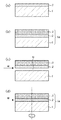
以下、本発明の好適な第1の実施形態として、基板から半導体層を分離する方法、或いは、基板から分離された半導体層を製造する方法について説明する。図1は、基板から半導体層を分離する方法、或いは、基板から分離された半導体層を製造する方法を概略的に示す図である。
[First Embodiment (Separation Method)]
Hereinafter, a method for separating a semiconductor layer from a substrate or a method for manufacturing a semiconductor layer separated from a substrate will be described as a preferred first embodiment of the present invention. FIG. 1 is a diagram schematically showing a method for separating a semiconductor layer from a substrate or a method for producing a semiconductor layer separated from a substrate.
まず、図1(a)に示す分離層形成工程において、Ge基板等の結晶性を有するシード基板1の上に、シード基板1とは格子定数の異なる半導体層、例えばAlAs又はInGaAsからなる分離層2をヘテロエピタキシャル成長させる。 First, in the separation layer forming step shown in FIG. 1A, a semiconductor layer having a lattice constant different from that of the seed substrate 1, such as a separation layer made of AlAs or InGaAs, on a seed substrate 1 having crystallinity such as a Ge substrate. 2 is heteroepitaxially grown.
次いで、図1(b)に示す半導体層形成工程において、分離層2の上にGaAs等の半導体層3を形成し、基板1、分離層2及び半導体層3を含む複合部材1aを形成する。この際に、半導体層3に半導体素子を形成することもできる。
次いで、図1(c)に示す分離工程において、分離層2を利用して複合部材1aから半導体層3を分離する。半導体層3の分離は、例えば、分離層2の内部、及び/又は、分離層2と半導体層3との界面、及び/又は、分離層2と基板1との界面に、複合部材1aの面方向に沿って広がる亀裂を形成することによってなされうる。なお、図1(c)には、分離層2と基板1との界面に、複合部材1aの面方向に沿った亀裂cを形成することにより、複合部材1aから半導体層3が分離される様子が模式的に示されている。
1B, a
Next, in the separation step shown in FIG. 1C, the
例えば、Ge基板等の結晶性を有するシード基板1の上に、基板1とは格子定数及び/又は熱膨張係数の異なるInGaAs等の分離層2をヘテロエピタキシャル成長させ、分離層2上にGaAs等の半導体層3を形成することにより、分離層2の内部、及び/又は、分離層2と半導体層3との界面、及び/又は、分離層と基板1との界面に、格子定数及び/又は熱膨張係数の不整合に起因する歪みエネルギーを集中的に生じさせることができる。そして、その後に、複合部材(複合基板)1aの全体、又は、その一部(例えば、分離層2の内部、及び/又は、分離層2と半導体層3との界面、及び/又は、分離層2と基板1との界面)に、分離を誘発するための力(分離誘発力)を外部から印加することにより、複合部材1aの内部に生じている歪みエネルギーを利用して複合部材1aから半導体層2を分離することができる。ここで、複合部材1aの全体又は一部に分離誘発力を印加することにより、複合部材1a(或いは、半導体層3、分離層2、基板1)の面方向に沿って平面的に分布する歪エネルギーを有する部分に選択的に亀裂を発生させることができる。分離誘発力は、必ずしも、半導体層3が完全に複合部材1aから分離されるまで印加し続ける必要はない。複合部材1aに部分的に亀裂が生じた後は、外部からの力の印加を停止した場合においても、その部分的な亀裂によって新たな歪エネルギーが発生して、それによって自己促進的に亀裂が広がって分離層3が複合部材から完全に分離されることもある。
シード基板1とそれから分離すべき半導体層2との間に分離層2を設けることにより、半導体層2に大きなダメージを与えることなく、分離層2の内部、及び/又は、分離層2と半導体層3との界面、及び/又は、分離層2と基板1との界面のみに亀裂を生じさせて、基板1から半導体層2を分離することができる。
シード基板1は、単結晶構造を有する材料により構成されることが望ましく、Ge基板のほか、例えば、Al2O3、SiC、GaAs、InP、Siの基板が好適である。
For example, on a seed substrate 1 having crystallinity such as a Ge substrate, a
By providing the
The seed substrate 1 is preferably made of a material having a single crystal structure, and in addition to a Ge substrate, for example, an Al 2 O 3 , SiC, GaAs, InP, or Si substrate is suitable.
分離層2は、シード基板1とは格子定数及び/又は熱膨張係数の異なる材料により構成されるべきであり、InGaAsのほか、例えば、GaN、InGaN、AlGaN、AlN、AlAs、AlGaAs、InAlAs、InGaAlP、InGaAsP、InGaPの化合物半導体材料が好適である。
The
半導体層3は、GaAsのほか、例えば、GaN、AlGaAs、InP、InGaN、AlGaN、AlN、AlAs、InGaAs、InAlAs、InGaAlP、InGaAsP、InGaPのいずれかの材料を含む化合物半導体材料が好適である。
The
複合部材から半導体層を分離する分離工程では、分離層2又はその近傍に流体Wを吹き付けて、分離層2の内部、及び/又は、分離層2と半導体層3との界面、及び/又は、分離層2と基板1との界面に流体Wを注入することにより複合部材1aの当該注入部分に亀裂を発生させて分離を行うことが好適である。
In the separation step of separating the semiconductor layer from the composite member, the fluid W is sprayed on the
ここで、分離層の一例としてのAlAsエピタキシャル成長層は、半導体層の一例としてのGaAs層に対して107もの極めて高い選択エッチング特性を有する。この特性を利用して、流体の導入部分を形成することにより、分離の開始位置をより確実に分離層又はその界面に限定することができる。 Here, the AlAs epitaxial growth layer as an example of the separation layer and has a very high selectivity etching characteristic 107 as against GaAs layer as an example of the semiconductor layer. By utilizing this characteristic to form the fluid introduction portion, the separation start position can be more reliably limited to the separation layer or its interface.
流体Wの注入による分離方法によれば、格子定数及び/又は熱膨張係数の不整合に起因して分離層2の内部、及び/又は、分離層2と半導体層3との界面、分離層2と及び基板1との界面に生じた歪みエネルギーと、流体Wの注入によるエネルギーとによって、分離層2の内部、及び/又は、分離層2と半導体層3との界面、分離層2と及び基板1との界面に亀裂を生じさせ、これを面方向に広げることができる。
半導体層の分離工程では、図1(d)に例示的に示すように、複合部材1aをその面方向に対して略垂直な軸を中心として回転させながら分離層2又はその近傍に流体Wを吹き付けると、基板1の外周部から中心部に向かって渦巻き状に分離を進行させることができる。
According to the separation method by the injection of the fluid W, the
In the semiconductor layer separation step, as illustrated in FIG. 1D, the fluid W is applied to the
流体としては、水等の液体のほか、空気、不活性ガス、エッチングガス等の気体を利用することができる。また、複合部材の分離層2又はその近傍に流体を吹き付ける代わりに、チャンバ内に複合部材を収容して該複合部材に流体によって圧力を印加することもできる。
As the fluid, in addition to liquids such as water, gases such as air, inert gas, and etching gas can be used. Further, instead of spraying fluid on the
以上のような本発明の好適な実施形態の方法によれば、分離の際に半導体層3及びシード基板1に与えられるダメージは、レーザーリフトオフ法に比較して大幅に低減される。よって、その後に半導体層3に形成される半導体素子の素子特性を良好にすることができる。
According to the method of the preferred embodiment of the present invention as described above, the damage given to the
また、本発明の好適な実施形態の方法によれば、半導体層3が分離された後のシード基板1を原料として再使用することが可能である。すなわち、分離後のシード基板1を原料として分離層形成工程、半導体層形成工程、分離工程の処理を複数回繰り返し施すことにより、半導体基板の製造コストを大幅に低減することができる。
Further, according to the method of the preferred embodiment of the present invention, the seed substrate 1 after the
また、本発明の好適な実施形態の方法によれば、シード基板1として、透過性基板のほか、非透過性基板も利用することができる。
[第2の実施形態(基板の製法)]
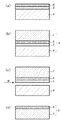
以下、本発明の好適な第2の実施形態として、半導体層を有する基板の製造方法について説明する。図2は、半導体層を有する基板の製造方法を概略的に示す図である。
In addition, according to the method of the preferred embodiment of the present invention, a non-transmissive substrate can be used as the seed substrate 1 in addition to the transmissive substrate.
[Second Embodiment (Manufacturing Method of Substrate)]
Hereinafter, a method for manufacturing a substrate having a semiconductor layer will be described as a second preferred embodiment of the present invention. FIG. 2 is a diagram schematically showing a method for manufacturing a substrate having a semiconductor layer.
まず、図2(a)に示す工程(分離層形成工程、半導体層形成工程)において、Ge基板等の結晶性を有する第1基板(シード基板)4の上に、第1基板4とは格子定数の異なる半導体層、例えばInGaAsからなる分離層5をヘテロエピタキシャル成長させる。次いで、分離層5の上にGaAs等の半導体層6を形成する。
First, in the steps shown in FIG. 2A (separation layer forming step, semiconductor layer forming step), the
次いで、図2(b)に示す接合工程において、半導体層6を内側にして第1基板4をSi基板等の第2基板(ハンドル基板)7に接合して複合部材(複合基板)8を形成する。この接合において、それぞれの接合面に金属膜を形成し、金属面同士の接合とすることで、接合に必要な圧力や温度の制限を緩和することも可能である。この金属層は、接合材料として好適なほか、光反射層としてデバイス性能の向上に寄与する。
Next, in the bonding step shown in FIG. 2B, the
次いで、図2(c)に示す分離工程において、複合部材8の分離層5の内部、及び/又は、分離層5と半導体層6との界面、及び/又は、分離層5と第1基板4との界面に面方向に広がる亀裂を生じさせて、半導体層6及び第2基板7を複合部材8から分離する。以上の工程により、半導体層6が第1基板4から第2基板7に移設され、図2(d)に示すように、第2基板7の上に半導体層6を有する基板9が得られる。この分離には、例えば、第1の実施形態で説明した方法を適用することができる。
例えば、Ge基板等の結晶性を有する第1基板(シード基板)4の上に、第1基板4とは格子定数及び/又は熱膨張係数の異なるInGaAs等の分離層5をヘテロエピタキシャル成長させ、分離層5上にGaAs等の半導体層6を形成し、半導体層6を内側にして第1基板4をSi等の第2基板(ハンドル基板)7に接合して複合部材8を形成することにより、分離層5の内部、及び/又は、分離層5と半導体層6との界面、及び/又は、分離層5と第1基板4との界面に、格子定数及び/又は熱膨張係数の不整合に起因する歪みエネルギーを集中的に生じさせることができる。そして、その後、複合部材8の全体、又は、その一部(例えば、分離層5の内部、及び/又は、分離層5と半導体層6との界面、及び/又は、分離層5と第1基板4との界面)に、分離誘発力を印加することにより、複合部材8の内部に生じている歪エネルギーを利用して複合部材8から半導体層6及び第2基板7を分離することができる。
第1基板(シード基板)4は、単結晶構造を有する材料により構成されることが望ましく、Ge基板のほか、例えば、Al2O3、SiC、GaAs、InP、Siの基板が好適である。
Next, in the separation step shown in FIG. 2C, the inside of the
For example, on a first substrate (seed substrate) 4 having crystallinity such as a Ge substrate, an
The first substrate (seed substrate) 4 is preferably made of a material having a single crystal structure, and in addition to a Ge substrate, for example, an Al 2 O 3 , SiC, GaAs, InP, or Si substrate is suitable.
分離層5は、第1の基板4とは格子定数及び/又は熱膨張係数の異なる材料により構成されるべきであり、InGaAsのほか、例えば、GaN、InGaN、AlGaN、AlN、AlAs、AlGaAs、InAlAs、InGaAlP、InGaAsP、InGaPの化合物半導体材料が好適である。
The
半導体層6は、GaAsのほか、例えば、GaN、AlGaAs、InP、InGaN、AlGaN、AlN、AlAs、InGaAs、InAlAs、InGaAlP、InGaAsP、InGaPのいずれかの材料を含む化合物半導体材料が好適である。 The semiconductor layer 6 is preferably a compound semiconductor material including, in addition to GaAs, for example, any material of GaN, AlGaAs, InP, InGaN, AlGaN, AlN, AlAs, InGaAs, InAlAs, InGaAlP, InGaAsP, and InGaP.
第2基板7は、Si等の半導体基板のほか、例えば、Al、Cu、Cu−W等の金属基板、ガラス等の絶縁性基板、プラスチック等の可撓性基板が好適である。
The
複合部材から半導体層及び第2基板を分離する工程では、分離層5又はその近傍に流体(液体、又は、気体)Wを吹き付け、分離層5の内部、及び/又は、分離層5と半導体層6との界面、分離層5と第1基板4との界面に流体Wを注入することにより複合部材の当該注入部分に亀裂を発生させて分離を行うことが好適である。
In the step of separating the semiconductor layer and the second substrate from the composite member, a fluid (liquid or gas) W is sprayed on the
[第3の実施形態(半導体素子の製造方法)]
以下、本発明の好適な第3の実施形態として、半導体素子を有する半導体層又は基板の製造方法について説明する。図3は、半導体素子を有する半導体層又は基板の製造方法を示す概略的に示す図である。
[Third Embodiment (Semiconductor Device Manufacturing Method)]
Hereinafter, as a preferred third embodiment of the present invention, a method for manufacturing a semiconductor layer or substrate having a semiconductor element will be described. FIG. 3 is a diagram schematically showing a method for manufacturing a semiconductor layer or substrate having a semiconductor element.
まず、図3(a)に示す工程(分離層形成工程、半導体層形成工程)において、Ge基板等の結晶性を有する第1基板(シード基板)10の上に、第1基板10とは格子定数の異なる半導体層、例えばInGaAsからなる分離層11をヘテロエピタキシャル成長させる。次いで、分離層11の上にGaAs等の半導体層12を形成する。
First, in the steps shown in FIG. 3A (separation layer forming step, semiconductor layer forming step), the
次いで、図3(b)に示す半導体素子形成工程において、半導体層12にLED等の半導体素子13を形成する。なお、典型的には、半導体素子形成工程では、単一の半導体素子が形成されるのではなく、複数の半導体素子のほか、それらを連結する配線等を含む半導体回路が形成され得る。
Next, in a semiconductor element formation step shown in FIG. 3B, a
次いで、図3(c)に示す接合工程において、半導体層12を内側にして第1基板10を例えばSi基板等の第2基板(ハンドル基板)14に接合して複合部材(複合基板)15を形成する。
Next, in the bonding step shown in FIG. 3C, the
次いで、図1(d)に示す分離工程において、複合部材15の分離層11の内部、及び/又は、分離層11と半導体層12との界面、及び/又は、分離層第1の基板10との界面に面方向に広がる亀裂を生じさせて、半導体素子13を有する半導体層12及び第2基板14を複合部材15から分離する。以上の工程により、半導体素子13を有する半導体層12が第1基板(シード基板)10から第2基板(ハンドル基板)14へ移設され、図3(e)に示すように、第2基板14の上に、半導体素子13が形成された半導体層12を有する基板(或いは半導体デバイス)16が得られる。この分離には、例えば、第1の実施形態で説明した方法を適用することができる。
なお、半導体素子13を半導体層12の上に形成した後に、第1基板10を第2基板14に接合する方法のほか、分離により半導体層12を第1基板10から第2基板14へ移設した後に、移設された半導体層12に半導体素子13を形成してもよい。
Next, in the separation step shown in FIG. 1D, the inside of the
In addition to the method of bonding the
例えば、Ge基板等の結晶性を有する第1基板(シード基板)10の上に、第1基板10とは格子定数及び/又は熱膨張係数の異なるInGaAs等の分離層11をヘテロエピタキシャル成長させ、分離層11上にGaAs等の半導体層12を形成し、半導体層12にLED等の半導体素子13を形成し、半導体層12を内側にして第1基板(シード基板)10をSi等の第2基板(ハンドル基板)14に接合して複合部材15を形成することにより、分離層11の内部、及び/又は、分離層11と半導体層12との界面、分離層11と第1の基板10との界面に、格子定数及び/又は熱膨張係数の不整合に起因する歪みエネルギーを集中的に生じさせることができる。そして、その後、複合部材15の全体、又は、その一部(例えば、分離層11の内部、及び/又は、分離層11と半導体層12との界面、分離層11と第1基板10との界面)に分離誘発力を印加することにより、複合部材15の内部に生じている歪エネルギーを利用して複合部材15から半導体層12及び第2基板14を分離することができる。
第1基板(シード基板)10は、単結晶構造を有する材料により構成されることが望ましく、Ge基板のほか、例えば、Al2O3、SiC、GaAs、InP、Siの基板が好適である。
For example, on a first substrate (seed substrate) 10 having crystallinity such as a Ge substrate, an
The first substrate (seed substrate) 10 is preferably made of a material having a single crystal structure, and an Al 2 O 3 , SiC, GaAs, InP, or Si substrate is preferable in addition to a Ge substrate.
分離層11は、第1の基板10とは格子定数及び/又は熱膨張係数の異なる材料により構成されるべきであり、InGaAsのほか、例えば、GaN、InGaN、AlGaN、AlN、AlAs、AlGaAs、InAlAs、InGaAlP、InGaAsP、InGaPの化合物半導体材料が好適である。
The
半導体層12は、GaAsのほか、例えば、GaN、AlGaAs、InP、InGaN、AlGaN、AlN、AlAs、InGaAs、InAlAs、InGaAlP、InGaAsP、InGaPのいずれかの材料を含む化合物半導体材料が好適である。
In addition to GaAs, the
半導体素子13としては、LED(発光ダイオード)やレーザー等の発光素子、X線等の放射線を検出する受光素子、太陽電池等の光電変換素子、トランジスタ、ダイオード、キャパシタ等の素子が好適である。ここで、半導体素子13の形成工程(図3(b))は、半導体素子を覆う絶縁層を形成する工程、更には、その絶縁層を平坦化する工程を含むことが好ましい。
As the
第2基板(ハンドル基板)14は、Si等の半導体基板のほか、例えば、Al、Cu等の金属基板、ガラス等の絶縁性基板、プラスチック等の可撓性基板が好適である。 The second substrate (handle substrate) 14 is preferably a semiconductor substrate such as Si, a metal substrate such as Al or Cu, an insulating substrate such as glass, or a flexible substrate such as plastic.
また、第2基板14に、半導体素子13を駆動するための駆動回路が設けられていること、及び/又は、第2基板14が回路パターンが形成されたプリント基板であることが好適である。この場合、半導体素子13を含む回路の接続電極と第2基板の駆動回路の接続電極またはプリント基板の接続電極とが電気的に接続される。
In addition, it is preferable that a drive circuit for driving the
複合部材から半導体層及び第2基板を分離する工程では、分離層11又はその近傍に流体(液体、又は、気体)Wを吹き付け、分離層11の内部、及び/又は、分離層11と半導体層12との界面、及び/又は、分離層11と第1基板10との界面に流体Wを注入することにより複合部材の当該注入部分に亀裂を発生させて分離を行うことが好適である。
In the step of separating the semiconductor layer and the second substrate from the composite member, fluid (liquid or gas) W is sprayed on the
以下、本発明の具体的な実施例を説明するが、本発明は、これらの実施例に限定されない。 [実施例1]
まず、MOCVD法により、Ge基板(シード基板)1上に、InGaAs層2(厚さ10nm)をヘテロエピタキシャル成長させ(図1(a))、その上にGaAs層3(厚さ200μm)をエピタキシャル成長させて複合部材1aを形成する(図1(b))。
Hereinafter, specific examples of the present invention will be described, but the present invention is not limited to these examples. [Example 1]
First, an InGaAs layer 2 (
次いで、複合部材1aの側面からInGaAs層2に対して分離誘発力を印加する。具体的には、数M〜100MPaの圧力をかけた純水を口径0.1mmの細いノズルから吹き出すいわゆるウォータジェットWをInGaAs層2の側面又はその近傍に吹き付けることにより、InGaAs層2の内部、及び/又は、InGaAs層2とGaAs層3との界面、及び/又は、InGaAs層2とGe基板1との界面に面方向に広がる亀裂を生じさせて、複合部材1a(Ge基板1)からGaAs層3を分離することができる(図1(c))。
Next, a separation inducing force is applied to the
分離後のGe基板は、必要に応じて、その表面に研磨、エッチング等の平坦化処理を施すことにより、繰り返して使用することができる。 The separated Ge substrate can be used repeatedly by subjecting the surface thereof to a planarization treatment such as polishing or etching as necessary.
[実施例2]
まず、MOCVD法により、Ge基板(シード基板)4上に、InGaAs層5(厚さ10nm)をヘテロエピタキシャル成長させ、その上にGaAs層6(厚さ3μm)をエピタキシャル成長させる(図2(a))。
[Example 2]
First, an InGaAs layer 5 (
次いで、GaAs層6を内側にしてGe基板4をSi基板(ハンドル基板)7に接合して複合部材8を形成する(図2(b))。ここで、接合に先立って、GaAs層6とSi基板7の各表面上にCr膜(厚さ10nm)、Au膜(厚さ200nm)を順次形成し(不図示)、その後、両表面上のAu膜同士を密着させ、圧力を印加しながら加熱することにより、充分な接合強度を有する複合部材8が得られる。
Next, the
次いで、複合部材8の側面からInGaAs層5に対して分離誘発力を印加する。具体的には、数M〜100MPaの圧力をかけた純水を口径0.1mmの細いノズルから吹き出すいわゆるウォータジェットWをInGaAs層5の側面又はその近傍に吹き付けることにより、InGaAs層5の内部、及び/又は、InGaAs層5とGaAs層6との界面、及び/又は、InGaAs層5とGe基板4との界面に面方向に広がる亀裂を生じさせて、複合部材8(Ge基板4)からGaAs層6を分離することができる(図2(c))。
Next, a separation inducing force is applied to the
これにより、Si基板7上に金属層(不図示)を介してGaAs層6を有する半導体基板9が得られる。
Thereby, the semiconductor substrate 9 having the GaAs layer 6 on the
また、分離後のGe基板は再使用が可能である。必要に応じて、分離後のGe基板の表面に研磨、エッチング等の平坦化処理を施すことにより、繰り返し使用することができる。 Further, the separated Ge substrate can be reused. If necessary, the surface of the Ge substrate after separation can be repeatedly used by performing a planarization treatment such as polishing and etching.
この実施例では、歪エネルギーを内在する分離層を一層のInGaAs層で構成したが、In組成の異なる複数の層で構成することも可能である。 In this embodiment, the separation layer containing the strain energy is composed of a single InGaAs layer, but it can also be composed of a plurality of layers having different In compositions.
例えば、Inの組成比が1%より大きいInGaAs層はGe基板より格子定数が大きいが、Inの組成比が1%以下のInGaAs層はGe基板より格子定数が小さいので、引っ張り、圧縮の双方の歪を内在させることが可能である。また、InGaAs層に替えてInGaP層またはInGaAsP層等の組成材料でも、歪の成分、大きさを制御可能である。 For example, an InGaAs layer with an In composition ratio greater than 1% has a lattice constant larger than that of a Ge substrate, but an InGaAs layer with an In composition ratio of 1% or less has a lattice constant smaller than that of a Ge substrate. It is possible to make distortion inherent. Further, the strain component and magnitude can be controlled by using a composition material such as an InGaP layer or an InGaAsP layer instead of the InGaAs layer.
また、GaAs層とSi基板とをAu膜を介して接合させているが、GaAs層及びSi基板の表面に真空状態でスパッタ・クリーニングを施し、その後、その表面同士を密着させて圧力を印加することにより、GaAs層とSi基板とを直接接合させることも可能である。 In addition, the GaAs layer and the Si substrate are bonded via the Au film, but the surface of the GaAs layer and the Si substrate is sputter-cleaned in a vacuum state, and then the surfaces are brought into close contact with each other to apply pressure. Thus, the GaAs layer and the Si substrate can be directly bonded.
[実施例3]
この実施例では、分離を更に容易に行うための分離補助層を利用する方法を説明する。
[Example 3]
In this embodiment, a method of using a separation assisting layer for performing separation more easily will be described.
まず、MOCVD法により、Ge基板(シード基板)17上に、AlAs層18(厚さ50nm)、InGaAs層19(Inの組成0.2、厚さ10nm)、GaAs層20(厚さ3μm)を連続的にエピタキシャル成長させる(図4(a))。ここで、AlAs層18は分離補助層として、InGaAs層19は分離層として機能する。
First, an AlAs layer 18 (thickness 50 nm), an InGaAs layer 19 (In composition 0.2,
次いで、GaAs層20を内側にしてGe基板17をSi基板21に接合して複合部材22を形成する(図4(b))。また、接合に先立って、GaAs層20とSi基板21の各表面上にCr膜(厚さ10nm)、Au膜(厚さ200nm)を順次形成し(不図示)、その後、両表面上のAu膜同士を密着させ、圧力を印加しながら加熱することにより、充分な接合強度を有する複合部材22が得られる。
Next, the
次いで、複合部材22を硫酸加水液(エッチング液)中に浸漬して、GaAs層20/InGaAs層19を部分的に除去して、複合部材22の周辺部にAlAs層18の側面を露出させ、AlAs層18の周辺部をフッ酸加水溶液(エッチング液)によって選択的にエッチング除去して、複合部材22の周辺部に凹部23を形成する。この凹部23は、分離のために注入される流体をAlAs層18又はその界面にガイドして、分離のための力をAlAs層18又はその界面に集中させるように機能し得る。AlAsは、GaAs、InGaAsに比べてエッチングが格段に速く進む上、水分で酸化されたその酸化物は水溶性であるため、ウォータジェットWによる分離中に、複合部材22の周辺部のAlAs層18が選択的にエッチングされた領域が形成され、ウォータジェットの純粋に溶解する作用も期待される。
Next, the
次いで、数M〜100MPaの圧力をかけた純水を口径0.1mmの細いノズルから吹き出すいわゆるウォータジェットWを複合部材22の凹部23又はその近傍に吹き付ける。ウォータジェットWが複合部材22を2枚の基板に分割する力(2枚の基板に分離された部分を引き離す力)が凹部23に集中することにより、複合部材22は、蓄積された歪エネルギーが開放されながら2枚の基板に分割される。(図4(c))
これにより、Si基板21の上にAu及びCrからなる金属層(不図示)を介してGaAs層20を有する半導体基板24を得ることができる。
Next, a so-called water jet W that blows pure water applied with a pressure of several M to 100 MPa from a thin nozzle having a diameter of 0.1 mm is blown to the
Thereby, the
この実施例では、一対の分離層及び分離補助層を形成したが、例えば、複数対の分離層及び分離補助層を形成してもよいし、In組成の異なる層を分離層及び分離補助層として形成してもよい。 In this embodiment, a pair of separation layers and auxiliary separation layers are formed. For example, a plurality of pairs of separation layers and auxiliary separation layers may be formed, or layers having different In compositions may be used as the separation layers and auxiliary separation layers. It may be formed.
分離補助層は、例えば、分離補助層の上下に接する層よりAlを多く含むようにその組成が決定されることが好ましい。分離補助層は、AlAsのほか、例えば、AlxGa1−xAs(x>0.95)で示される材料により構成されることが好ましい。 The composition of the separation assisting layer is preferably determined so as to contain more Al than the layers in contact with the upper and lower sides of the separation assisting layer. The separation assisting layer is preferably made of a material represented by, for example, AlxGa1-xAs (x> 0.95) in addition to AlAs.
[実施例4]
この実施例は、分離層を、基板より格子定数の大きい層と小さい層の積層構成にするものである。
[Example 4]
In this embodiment, the separation layer has a laminated structure of a layer having a larger lattice constant and a layer having a smaller lattice constant than the substrate.
まず、MOCVD法により、Ge基板上に、格子定数がGeより小さいInの組成が0.28のInGaP層(厚さ5nm)、格子定数がGeより大きいInの組成が0.2のInGaAs層(厚さ5nm)、GaAs層(厚さ3μm)を連続的にエピタキシャル成長させる。
First, by MOCVD, an InGaP layer (
この構成により、InGaP層とInGaAs層との界面には大きな歪エネルギーが集中的に内在するが、InGaP層とInGaAs層との積層構成からなる分離層全体では格子定数の大小が平均化されるので、Ge基板とInGaP層、及びInGaAs層とGaAs層の界面の格子定数差は緩和される。よって、結晶性の良好なGaAs層が得られる。 With this configuration, large strain energy is concentrated and concentrated at the interface between the InGaP layer and the InGaAs layer. However, the size of the lattice constant is averaged in the entire separation layer composed of the stacked configuration of the InGaP layer and the InGaAs layer. The lattice constant difference at the interface between the Ge substrate and the InGaP layer and between the InGaAs layer and the GaAs layer is relaxed. Therefore, a GaAs layer with good crystallinity can be obtained.
その後、実施例3と同様に、Ge基板にSi基板を接合し、次いで分離を行う。 Thereafter, similarly to Example 3, a Si substrate is bonded to the Ge substrate, and then separated.
[実施例5]
図5に示すように、Ge基板25の上に、AlAs層26からなる分離補助層、InGaAs層27からなる分離層を形成し、その表面に、n型GaAs層28、n型AlxGa1-xAs層29、n型AlyGa1-yAs層30、n型AlxGa1-xAs層31、n型GaAs層32(y<x)を順次エピタキシャル成長させる(図5(a))。
[Example 5]
As shown in FIG. 5, a separation auxiliary layer made of an AlAs layer 26 and a separation layer made of an
エピタキシャル成長層の不純物濃度や厚さは、デバイスの設計に依存するが、典型的な構成は以下の通りである。 The impurity concentration and thickness of the epitaxial growth layer depend on the design of the device, but a typical configuration is as follows.
n型GaAs層28 : 0.05〜0.5μm ; Siドーピング
n型Al0.35Ga0.65As層29 : 1μm ; Siドーピング
n型Al0.13Ga0.87As層30 : 0.5μm ; Siドーピング
n型Al0.35Ga0.65As層31 : 1μm ; Siドーピング
n型GaAs層32 : 0.1〜0.5μm ; Siドーピング
Siドーピングは、キャリヤ濃度が1017/cm3程度となるように行った。
n-type GaAs layer 28: 0.05 to 0.5 μm; Si-doped n-type Al 0.35 Ga 0.65 As layer 29: 1 μm; Si-doped n-type Al 0.13 Ga 0.87 As layer 30: 0.5 μm; Si-doped n-type Al 0. 35Ga0.65As layer 31: 1 μm; Si doping n-type GaAs layer 32: 0.1-0.5 μm; Si doping Si doping was performed so that the carrier concentration was about 10 17 / cm 3 .
次いで、n型GaAs層32の上にn型金属電極層33を形成し、この面にSi基板34を接合させて複合部材35を形成する(図5(a))。
Next, an n-type
次いで、AlAs層26からなる分離補助層、InGaAs層27からなる分離層の側面に細く絞った高圧水流(ウォータジェット)Wを吹き付ける。これにより、ウォータジェットWが複合部材35を2枚の基板に分割する力(2枚の基板に分離された部分を引き離す力)がAlAs層18の両側に加わって複合部材22が2枚の基板に分割される。 次いで、n型AlxGa1−xAs層29に面発光型のLEDを形成する(図5(c))。具体的には、スパッタにより絶縁層36を全面に形成し、フォトリソグラフィー及びドライエッチングにより絶縁層36に窓を形成する。次いで、スパッタによりZnSiOを成膜し、その後、熱拡散を行うことにより、窓領域をp型領域37に転換する。そして、p側金属電極38をp型領域37上に形成する。
Next, a high-pressure water stream (water jet) W narrowly squeezed onto the side surfaces of the separation auxiliary layer made of the AlAs layer 26 and the separation layer made of the
このようにして、面発光型LED素子を得ることができる。 In this way, a surface emitting LED element can be obtained.
[実施例6]
まず、MOCVD法により、GaAs基板上にInGaAs層、GaAs層をエピタキシャル成長させる。InGaAs層は、Inの組成の増大とともに格子定数は大きくなるため、Inの組成の増大にともなってGaAs基板との格子定数の不整合が増加し、InGaAs層の内部に歪エネルギーが生じることになる。
[Example 6]
First, an InGaAs layer and a GaAs layer are epitaxially grown on a GaAs substrate by MOCVD. Since the lattice constant of the InGaAs layer increases as the In composition increases, the mismatch of the lattice constant with the GaAs substrate increases as the In composition increases, and strain energy is generated inside the InGaAs layer. .
この実施例では、GaAs基板上に、Inの組成が0.2のInGaAs層(厚さ10nm)とGaAs層(厚さ3μm)を連続的にエピタキシャル成長させる。
In this embodiment, an InGaAs layer (
次いで、GaAs層を内側にしてGaAs基板をSi基板に接合する。このとき、接合に先立って、GaAs層とSi基板の各表面上にCr膜(厚さ10nm)、Au膜(厚さ200nm)を順次成膜し、その後、両表面上のAu膜同士を密着させ、圧力を印加しながら加熱することにより、充分な接合強度を有する複合部材が得られる。
Next, the GaAs substrate is bonded to the Si substrate with the GaAs layer inside. At this time, prior to bonding, a Cr film (
次いで、複合部材の側面からInGaAs層に対して力を印加する。具体的には、数M〜100MPaの圧力をかけた純水を口径0.1mmの細いノズルから吹き出すいわゆるウォータジェットをInGaAs層の側面又はその近傍に吹き付けることにより、InGaAs層の内部、及び/又は、InGaAs層とGaAs層との界面、及び/又は、InGaAs層とGaAs基板との界面に面方向に広がる亀裂を生じさせて、複合部材(GaAs基板)からGaAs層を分離することができる。 Next, force is applied to the InGaAs layer from the side surface of the composite member. Specifically, a so-called water jet that blows pure water with a pressure of several M to 100 MPa from a thin nozzle having a diameter of 0.1 mm is blown to the side surface of the InGaAs layer or the vicinity thereof, and / or The GaAs layer can be separated from the composite member (GaAs substrate) by generating cracks extending in the surface direction at the interface between the InGaAs layer and the GaAs layer and / or at the interface between the InGaAs layer and the GaAs substrate.
これにより、Si基板上にAu、Crの金属層を介してGaAs層を有する半導体基板が得られる。 As a result, a semiconductor substrate having a GaAs layer on the Si substrate via the Au and Cr metal layers is obtained.
また、分離後のGaAs基板は再使用が可能である。必要に応じて、分離後のGaAs基板の表面に研磨、エッチング等の平坦化処理を施すことにより、繰り返し使用することができる。 Further, the separated GaAs substrate can be reused. If necessary, the surface of the separated GaAs substrate can be repeatedly used by performing a planarization process such as polishing or etching.
この実施例では、歪エネルギーを内在する分離層を一層のInGaAs層で構成したが、In組成の異なる複数の層で構成することも可能である。 In this embodiment, the separation layer containing the strain energy is composed of a single InGaAs layer, but it can also be composed of a plurality of layers having different In compositions.
例えば、InGaAs層はGaAs基板より格子定数が大きいが、InGaAs層に替えてInGaP層又はInGaAsP層を採用することによってGaAs基板より格子定数を小さくすることで、圧縮歪を内在させる構成も可能である。 For example, although the InGaAs layer has a larger lattice constant than the GaAs substrate, it is possible to adopt a configuration in which the compressive strain is inherent by making the lattice constant smaller than that of the GaAs substrate by adopting an InGaP layer or InGaAsP layer instead of the InGaAs layer. .
また、GaAs層とSi基板とをAu膜を介して接合しているが、GaAs層及びSi基板の表面に真空状態でスパッタ・クリーニングを施し、その後、その表面同士密着させて圧力を印加することにより、GaAs層とSi基板とを直接接合させることも可能である。 In addition, the GaAs layer and the Si substrate are bonded via the Au film, but the surface of the GaAs layer and the Si substrate is sputter-cleaned in a vacuum state, and then the surfaces are brought into close contact with each other to apply pressure. Thus, the GaAs layer and the Si substrate can be directly joined.
[実施例7]
この実施例では、分離を更に容易に行うための分離補助層を設ける。
[Example 7]
In this embodiment, a separation assisting layer is provided to make separation easier.
まず、MOCVD法により、GaAs基板上に、分離補助層としてのAlAs層(厚さ50nm)、分離層としてのInの組成が0.2のInGaAs層(厚さ10nm)、半導体層としてのGaAs層(厚さ3μm)を連続的にエピタキシャル成長させる。
First, by an MOCVD method, an AlAs layer (thickness 50 nm) as a separation auxiliary layer, an InGaAs layer (
次いで、GaAs層を内側にしてGaAs基板をSi基板に接合する。また、接合に先立ってGaAs層とSi基板の各表面上にCr膜(厚さ10nm)、Au膜(厚さ200nm)を順次成膜し、その後、両表面上にAu膜同士を密着させ、圧力を印加しながら加熱することにより、充分な接合強度を有する複合部材が得られる。
Next, the GaAs substrate is bonded to the Si substrate with the GaAs layer inside. Prior to the bonding, a Cr film (
次いで、この複合部材をAlAs層及びInGaAs層の近傍で分割するために、まず、複合部材の周辺部をエッチングする。エッチング液として硫酸:過酸化水素:水の混合液を用いて、複合部材の周辺部に凹部を形成する。AlAsは、GaAs、InGaAsに比べてエッチングが格段に速く進む上に、水分で酸化されたその酸化物は水溶性であるため、複合部材の周辺部のAlAs層が選択的にエッチングされた領域が形成される。 Next, in order to divide the composite member in the vicinity of the AlAs layer and the InGaAs layer, first, the peripheral portion of the composite member is etched. Using a mixed solution of sulfuric acid: hydrogen peroxide: water as an etching solution, recesses are formed in the periphery of the composite member. AlAs is etched much faster than GaAs and InGaAs, and the oxide oxidized with water is water-soluble. Therefore, there is a region where the AlAs layer in the peripheral part of the composite member is selectively etched. It is formed.
次いで、数M〜100MPaの圧力をかけた純水を口径0.1mmの細いノズルから吹き出すウォータジェットを複合部材の凹部又はその近傍に吹き付ける。純水に晒されたAlAs層は、酸化の進行とともに溶出するため、ウォータジェットの圧力が複合部材を2枚の基板に分割する力に加えて、AlAs層のエッチングが急速に進むことで、複合部材は分割される。 Next, a water jet that blows pure water applied with a pressure of several M to 100 MPa from a thin nozzle having a diameter of 0.1 mm is blown to or near the concave portion of the composite member. Since the AlAs layer exposed to pure water elutes as the oxidation progresses, the pressure of the water jet adds to the force that splits the composite member into two substrates, and the etching of the AlAs layer proceeds rapidly, resulting in a composite The member is divided.
これにより、Si基板上にAu及びCrからなる金属層を介してGaAs層を有する半導体基板を得ることができる。 Thereby, a semiconductor substrate having a GaAs layer on a Si substrate via a metal layer made of Au and Cr can be obtained.
この実施例では、一対の分離層及び分離補助層を形成したが、例えば、複数対の分離層及び分離補助層を形成してもよいし、In組成の異なる層を分離層及び分離補助層として形成してもよい
[実施例8]
この実施例は、分離層を、基板より格子定数の大きい層と小さい層の積層構成にするものである。
In this embodiment, a pair of separation layers and auxiliary separation layers are formed. For example, a plurality of pairs of separation layers and auxiliary separation layers may be formed, or layers having different In compositions may be used as the separation layers and auxiliary separation layers. [Example 8]
In this embodiment, the separation layer has a laminated structure of a layer having a larger lattice constant and a layer having a smaller lattice constant than the substrate.
まず、MOCVD法により、GaAs基板上に、格子定数がGaAsより小さいInの組成が0.28のInGaAsP層(厚さ5nm)、格子定数がGaAsより大きいInの組成が0.2のInGaAs層(厚さ5nm)、GaAs層(厚さ3μm)を連続的にエピタキシャル成長させる。
First, by MOCVD, an InGaAsP layer (
この構成により、InGaAsP層とInGaAs層との界面には大きな歪エネルギーが集中的に内在するが、InGaAsP層とInGaAs層との積層構成からなる分離層全体では格子定数の大小が平均化されるので、GaAs基板とInGaAsP層との界面、並びに、InGaAs層とGaAs層との界面において、格子定数の不整合は緩和される。よって、結晶性の良好なGaAs層が得られる。 With this configuration, large strain energy is concentrated and concentrated at the interface between the InGaAsP layer and the InGaAs layer, but the size of the lattice constant is averaged in the entire separation layer composed of the stacked configuration of the InGaAsP layer and the InGaAs layer. At the interface between the GaAs substrate and the InGaAsP layer and at the interface between the InGaAs layer and the GaAs layer, the mismatch of the lattice constant is alleviated. Therefore, a GaAs layer with good crystallinity can be obtained.
その後、実施例7と同様に、GaAs基板にSi基板を接合し、次いで分離を行う。 Thereafter, as in Example 7, the Si substrate is bonded to the GaAs substrate and then separated.
[実施例9]
この実施例は、分離層を、基板とは熱膨張係数の異なる層により構成するものである。このような分離層によれば、基板および分離層上の半導体層と格子定数の不整合を小さくできるので、分離層の上に厚い半導体層を形成しても、欠陥の発生を極めて小さく抑制できる。
[Example 9]
In this embodiment, the separation layer is composed of a layer having a coefficient of thermal expansion different from that of the substrate. According to such an isolation layer, the mismatch of the lattice constant with the semiconductor layer on the substrate and the isolation layer can be reduced, so that even when a thick semiconductor layer is formed on the isolation layer, the occurrence of defects can be suppressed to an extremely low level. .
まず、MOCVD法により、GaAs基板上に、格子定数がGaAsとほぼ等しいInの組成が0.51のInGaP層(厚さ20nm)、GaAs層(厚さ3μm)を連続的にエピタキシャル成長させる。
First, an InGaP layer (
InGaP層の熱膨張係数は5.926×10⁻⁶/degであり、GaAsの5.70×10−9/degと約4.2%の違いを有している。しかしながら、格子定数はほぼ等しいことから、GaAs基板とInGaP層、及びInGaP層とGaAs層の界面では、格子定数の不整合は緩和される。よって、結晶性の良好なGaAs層が得られる。 The thermal expansion coefficient of the InGaP layer is 5.926 × 10 −6 / deg, which is a difference of about 4.2% from 5.70 × 10 −9 / deg of GaAs. However, since the lattice constants are substantially equal, the mismatch of lattice constants is mitigated at the interface between the GaAs substrate and the InGaP layer and between the InGaP layer and the GaAs layer. Therefore, a GaAs layer with good crystallinity can be obtained.
その後、実施例7と同様に、GaAs基板にSi基板を接合し、次いで分離を行う。 Thereafter, as in Example 7, the Si substrate is bonded to the GaAs substrate and then separated.
[実施例10]
8インチ径のAl2O3基板を1000℃以上の高温で水素に曝して洗浄及び平坦化した後、水素のキャリヤガスにGa、Al有機金属化合物とNH3ガスを用いたMOCVD法により、AlN層を500℃で20〜100nmの厚みに堆積して緩衝層を形成する。この緩衝層は、微結晶粒界構造を有しており、500℃程度の低温で堆積しているため、1000℃程度の高温で成長する場合と比較すると空間的に均一かつ平坦に堆積することができる。その微結晶粒径の大きさはAlNの場合には十数nm程度ある。次いで、Al2O3基板の基板温度を1000℃程度に昇温し、この緩衝層の上にGaN層を形成し、更にその上部にLEDの活性層のためのPN接合の多層構造を形成した。
[Example 10]
After cleaning and planarizing an 8 inch diameter Al 2 O 3 substrate by exposing it to hydrogen at a high temperature of 1000 ° C. or higher, an AlN film is formed by MOCVD using Ga, Al organometallic compound and NH 3 gas as a hydrogen carrier gas. The layer is deposited at 500 ° C. to a thickness of 20-100 nm to form a buffer layer. Since this buffer layer has a microcrystalline grain boundary structure and is deposited at a low temperature of about 500 ° C., it is deposited spatially uniformly and flatly as compared with the case of growing at a high temperature of about 1000 ° C. Can do. In the case of AlN, the crystallite grain size is about a dozen nm. Next, the substrate temperature of the Al 2 O 3 substrate was raised to about 1000 ° C., a GaN layer was formed on the buffer layer, and a PN junction multilayer structure for the active layer of the LED was further formed thereon. .
次いで、Al2O3基板上のLED多層構造の上にPd膜、Au膜を順次堆積して金属電極層を形成する。他方の支持基板として8インチ径のSi基板を準備し、Si基板の表面にAl膜、Sn膜を順次成膜して金属電極層を形成する。Al金属層は、図6に示すように、Au等に比較して紫外光領域において高い反射率を有する。 Next, a Pd film and an Au film are sequentially deposited on the LED multilayer structure on the Al 2 O 3 substrate to form a metal electrode layer. An 8-inch diameter Si substrate is prepared as the other support substrate, and an Al film and an Sn film are sequentially formed on the surface of the Si substrate to form a metal electrode layer. As shown in FIG. 6, the Al metal layer has a higher reflectance in the ultraviolet region than Au or the like.
GaN系のデバイスの発光波長は、典型的には青、紫、紫外領域にあり、それに応じて最適な反射金属を選択することが必要となる。図5において、紫外領域まで反射率が維持できるのはAl、Rhなどが好適である。 The emission wavelength of a GaN-based device is typically in the blue, purple, and ultraviolet regions, and it is necessary to select an optimal reflective metal accordingly. In FIG. 5, Al, Rh, etc. are suitable for maintaining the reflectance up to the ultraviolet region.
その後、LED多層構造上の電極層とSi基板上の電極層とを互いの表面を密着させ、更に300℃で加熱処理して、接合界面のAu/Snを合金化させることにより融着させ、接合界面の接合強度を著しく強化した複合部材を得た。 Then, the electrode layer on the LED multilayer structure and the electrode layer on the Si substrate are brought into close contact with each other, further heat-treated at 300 ° C., and fused by alloying Au / Sn at the bonding interface, A composite member with significantly enhanced bonding strength at the bonding interface was obtained.
次いで、この複合部材を燐酸溶液に浸漬し、歪及び結晶欠陥が集中するAlNの緩衝層を、複合部材の外周端面の全周に沿って、数十ミクロン、端面から中心に向かって後退させて凹部を形成する。 Next, the composite member is immersed in a phosphoric acid solution, and an AlN buffer layer in which strain and crystal defects are concentrated is retracted from the end surface toward the center by several tens of microns along the entire outer peripheral end surface of the composite member. A recess is formed.
次いで、複合部材を略垂直に通る軸を中心に回転させながらこの凹部へ0.1mmに絞った純水の収束流体を0.3Nの圧力で注入し、AlN層の内部、及び/又は、AlN層とGaN層との界面、及び/又は、AlN層とAl2O3基板との界面で、Al2O3基板をGaN層にダメージを与えることなく分割することができた。その結果、その上部に形成されていたLED構造である多層膜がSi基板の上に移設された。 Next, a pure water converging fluid with a thickness of 0.1 mm is injected into the recess while rotating about the axis passing through the composite member substantially vertically, and the inside of the AlN layer and / or AlN is injected into the recess at a pressure of 0.3 N. The Al 2 O 3 substrate could be divided without damaging the GaN layer at the interface between the layer and the GaN layer and / or the interface between the AlN layer and the Al 2 O 3 substrate. As a result, the multilayer film which is the LED structure formed on the upper part was transferred onto the Si substrate.
LEDの発光波長を吸収するGaN層を化学機械研磨法(CMP)で除去した後、Ti膜、Al膜を順次堆積して、オーミック電極を形成し、メッシュ状にパターニングした。 After removing the GaN layer that absorbs the emission wavelength of the LED by chemical mechanical polishing (CMP), a Ti film and an Al film were sequentially deposited to form an ohmic electrode and patterned into a mesh.
この後、LED素子をチップ状に切断して、LEDチップを得ることができた。 Thereafter, the LED element was cut into chips to obtain an LED chip.
[実施例11]
実施例9と同様に、MOCVD法により、8インチ径のAl2O3基板上に微結晶粒界構造を有するGaN層からなる緩衝層をヘテロエピタキシャル成長させ、その上にGaN層を成長させる。
[Example 11]
Similar to Example 9, a buffer layer made of a GaN layer having a microcrystalline grain boundary structure is heteroepitaxially grown on an 8-inch diameter Al 2 O 3 substrate by MOCVD, and a GaN layer is grown thereon.
次いで、その上部にリッヂ型レーザーダイオードのデバイス層を積層した。デバイス層上にPd膜、Au膜を順次堆積して金属電極層を形成する。他方の支持基板として8インチ径のSi基板を準備し、Si基板の表面にTi膜、Au膜、Sn膜を順次堆積して金属電極層を形成する。 Next, a device layer of a ridge type laser diode was laminated thereon. A metal electrode layer is formed by sequentially depositing a Pd film and an Au film on the device layer. An 8-inch diameter Si substrate is prepared as the other supporting substrate, and a Ti film, an Au film, and an Sn film are sequentially deposited on the surface of the Si substrate to form a metal electrode layer.
その後、レーザーダイオードのデバイス層上の電極層とSi基板上の電極層とを互いの表面を密着させ、更に300℃で加熱処理して、接合界面のAu/Snを合金化させることにより融着させ、接合界面の接合強度を著しく強化した複合部材を得た。 Then, the electrode layer on the device layer of the laser diode and the electrode layer on the Si substrate are brought into close contact with each other and further heat-treated at 300 ° C. to alloy Au / Sn at the bonding interface, thereby fusing. As a result, a composite member in which the bonding strength at the bonding interface was remarkably enhanced was obtained.
次いで、この複合部材を燐酸溶液に浸漬し、歪及び結晶欠陥が集中するGaNの緩衝層を、複合部材の外周端面から全周に沿って、数十ミクロン、端面から中心に向かって後退させて凹部を形成する。 Next, the composite member is immersed in a phosphoric acid solution, and the GaN buffer layer in which strain and crystal defects are concentrated is retracted from the outer peripheral end surface of the composite member to the center by several tens of microns from the end surface toward the center. A recess is formed.
次いで、複合部材を略垂直に通る軸を中心に回転させながらこの凹部へ0.1mmに絞った純水の収束流体を0.3Nの圧力で注入し、GaNの緩衝層の内部及び/又はGaN層とAl2O3基板との界面で、GaN層にダメージを与えることなく分離することができた。その結果、その上部に形成されていたレーザーダイオード構造である多層膜がSi基板の上に移設された。 Then, a pure water converging fluid with a thickness of 0.1 mm is injected into the recess while rotating about the axis passing through the composite member substantially vertically, and the inside of the GaN buffer layer and / or GaN is injected into the recess at a pressure of 0.3 N. Separation was possible without damaging the GaN layer at the interface between the layer and the Al 2 O 3 substrate. As a result, a multilayer film having a laser diode structure formed on the upper portion was transferred onto the Si substrate.
従来、Al2O3基板上に作成されたレーザーダイオードの共振器部分の形成のために、活性層のへき開面が必要となるが、Al2O3基板のへき開性が乏しいために共振器の鏡端面の形成が困難であった。 Conventionally, in order to form the resonator section of the laser diode created Al 2 O 3 substrate, but cleavage plane of the active layer is required, the cavity for cleavage of the Al 2 O 3 substrate is poor Formation of the mirror end face was difficult.
この実施例にように、へき開性が高いSi基板をGaNのレーザーダイオードの支持基板として用いた場合には、容易な共振器の形成が可能となった。又、熱放散に優れたSi基板にレーザーが設置されているため、効率良く電力が供給される。 As in this example, when a Si substrate having a high cleavage property was used as a support substrate for a GaN laser diode, it was possible to easily form a resonator. In addition, since the laser is installed on the Si substrate excellent in heat dissipation, power is efficiently supplied.
[実施例12]
まず、MOCVD法により、8インチ径のAl2O3基板上に微結晶粒界構造を有するAlN層からなる緩衝層をヘテロエピタキシャル成長し、その上にGaN層を成長させた。
[Example 12]
First, a buffer layer made of an AlN layer having a microcrystalline grain boundary structure was heteroepitaxially grown on an 8-inch diameter Al2O3 substrate by MOCVD, and a GaN layer was grown thereon.
次いで、その上部に面発光レーザー(VCSEL)構造のデバイス層を形成した。熱放散が優れたCuを8インチに整形した支持基板上に、誘電体DBRミラーを堆積した。結晶成長中に半導体DBRミラーを介在させるよりも、支持基板上に誘電体DBRミラーを形成した方が、より材料選択(屈折率)が自由になり、結果として高性能な反射ミラーが形成され面発光レーザーの発光効率が向上する。 Next, a device layer having a surface emitting laser (VCSEL) structure was formed thereon. A dielectric DBR mirror was deposited on a support substrate in which Cu having excellent heat dissipation was shaped into 8 inches. Rather than interposing a semiconductor DBR mirror during crystal growth, forming a dielectric DBR mirror on a support substrate allows more freedom in material selection (refractive index), resulting in the formation of a high-performance reflective mirror. The luminous efficiency of the light emitting laser is improved.
次いで、両者を互いに密着させ、熱処理を施して接合強度を高めた複合部材を得た。 Subsequently, both were brought into close contact with each other, and heat treatment was performed to obtain a composite member having increased bonding strength.
次いで、この複合部材のAlN層の側面に向けて純水の収束流体を注入し、複合部材を分割し、高い反射率を持つ誘電体DBRミラー上に設置されたレーザーダイオード構造である多層膜がSi基板の上に移設された。 Subsequently, a convergent fluid of pure water is injected toward the side surface of the AlN layer of the composite member, the composite member is divided, and a multilayer film that is a laser diode structure installed on a dielectric DBR mirror having high reflectivity is formed. It was transferred onto the Si substrate.
その他に、Al2O3基板に変えてSiC基板を用いることも同様に可能である。 In addition, it is also possible to use a SiC substrate instead of the Al 2 O 3 substrate.
Claims (17)
シード基板上に分離補助層を形成する分離補助層形成工程と、
前記分離補助層上に分離層をヘテロエピタキシャル成長させる分離層形成工程と、
前記分離層上に半導体層を形成する半導体層形成工程と、
前記半導体層形成工程を経て形成される複合部材から前記分離層を利用して前記半導体層を分離する分離工程と、を含み、
前記分離補助層は、前記シード基板及び前記分離層に対して選択的にエッチングが可能な材料で形成される、
ことを特徴とする半導体層の製造方法。 A method for manufacturing a semiconductor layer, comprising:
A separation auxiliary layer forming step of forming a separation auxiliary layer on the seed substrate;
A separation layer forming step of heteroepitaxially growing the separation layer on the separation auxiliary layer;
A semiconductor layer forming step of forming a semiconductor layer on the separation layer;
A separation step of separating the semiconductor layer from the composite member formed through the semiconductor layer formation step using the separation layer , and
The separation auxiliary layer is formed of a material that can be selectively etched with respect to the seed substrate and the separation layer.
A method for manufacturing a semiconductor layer.
シード基板上に分離補助層を形成する分離補助層形成工程と、
前記分離補助層上に分離層をヘテロエピタキシャル成長させる分離層形成工程と、
前記分離層上に半導体層を形成する半導体層形成工程と、
前記半導体層形成工程を経て形成される複合部材から前記分離層を利用して前記半導体層を分離する分離工程と、を含み、
前記分離補助層は、それに接する層よりもAlを多く含む、
ことを特徴とする半導体層の製造方法。 A method for manufacturing a semiconductor layer, comprising:
A separation auxiliary layer forming step of forming a separation auxiliary layer on the seed substrate;
A separation layer forming step of heteroepitaxially growing the separation layer on the separation auxiliary layer;
A semiconductor layer forming step of forming a semiconductor layer on the separation layer;
A separation step of separating the semiconductor layer from the composite member formed through the semiconductor layer formation step using the separation layer , and
The separation auxiliary layer contains more Al than the layer in contact therewith,
A method for manufacturing a semiconductor layer.
シード基板上に分離補助層を形成する分離補助層形成工程と、
前記分離補助層上に分離層をヘテロエピタキシャル成長させる分離層形成工程と、
前記分離層上に半導体層を形成する半導体層形成工程と、
前記半導体層形成工程を経て形成される複合部材から前記分離層を利用して前記半導体層を分離する分離工程と、を含み、
前記分離補助層は、Al x Ga 1−x As(x>0.95)を満足する材料で構成される、
ことを特徴とする半導体層の製造方法。 A method for manufacturing a semiconductor layer, comprising:
A separation auxiliary layer forming step of forming a separation auxiliary layer on the seed substrate;
A separation layer forming step of heteroepitaxially growing the separation layer on the separation auxiliary layer;
A semiconductor layer forming step of forming a semiconductor layer on the separation layer;
A separation step of separating the semiconductor layer from the composite member formed through the semiconductor layer formation step using the separation layer , and
The separation auxiliary layer is made of a material that satisfies Al x Ga 1-x As (x> 0.95).
A method for manufacturing a semiconductor layer.
前記分離工程では、前記接合工程を経て形成される複合部材から、前記分離層を利用して、前記ハンドル基板とともに前記半導体層を分離することを特徴とする請求項1乃至請求項11のいずれか1項に記載の半導体層の製造方法。 After the semiconductor layer forming step and before the separation step, the separation auxiliary layer, the separation layer, and the seed substrate on which the semiconductor layer is formed are bonded to the handle substrate with the semiconductor layer inside. Further comprising a joining step
Wherein in the separation step, the composite member is formed through the bonding step, by using the separation layer, any one of claims 1 to 11 and separating the semiconductor layer with the handle substrate 2. A method for producing a semiconductor layer according to item 1.
シード基板上に分離補助層を形成する分離補助層形成工程と、
前記分離補助層上に分離層をヘテロエピタキシャル成長させる分離層形成工程と、
前記分離層上に半導体層を形成する半導体層形成工程と、
前記分離層及び前記半導体層が形成された前記シード基板を、前記半導体層を内側にして、ハンドル基板に接合する接合工程と、
前記接合工程を経て形成される複合部材から、前記分離層を利用して、前記ハンドル基板とともに前記半導体層を分離して、前記ハンドル基板上に前記半導体層を有する基板を得る分離工程と、を含み、
前記分離補助層は、前記シード基板及び前記分離層に対して選択的にエッチングが可能な材料で形成される、
ことを特徴とする基板の製造方法。 A method of manufacturing a substrate having a semiconductor layer,
A separation auxiliary layer forming step of forming a separation auxiliary layer on the seed substrate;
A separation layer forming step of heteroepitaxially growing the separation layer on the separation auxiliary layer;
A semiconductor layer forming step of forming a semiconductor layer on the separation layer;
A bonding step of bonding the seed substrate on which the separation layer and the semiconductor layer are formed to the handle substrate with the semiconductor layer inside;
A composite member formed through said bonding step, by using the separation layer, and separating the semiconductor layer with the handle substrate, and a separation step of obtaining a substrate having the semiconductor layer to the handle substrate Including
The separation auxiliary layer is formed of a material that can be selectively etched with respect to the seed substrate and the separation layer.
A method for manufacturing a substrate, comprising:
シード基板上に分離補助層を形成する分離補助層形成工程と、
前記分離補助層上に分離層をヘテロエピタキシャル成長させる分離層形成工程と、
前記分離層上に半導体層を形成する半導体層形成工程と、
前記分離層及び前記半導体層が形成された前記シード基板を、前記半導体層を内側にして、ハンドル基板に接合する接合工程と、
前記接合工程を経て形成される複合部材から、前記分離層を利用して、前記ハンドル基板とともに前記半導体層を分離して、前記ハンドル基板上に前記半導体層を有する基板を得る分離工程と、を含み、
前記分離補助層は、それに接する層よりもAlを多く含む、
を含むことを特徴とする基板の製造方法。 A method of manufacturing a substrate having a semiconductor layer,
A separation auxiliary layer forming step of forming a separation auxiliary layer on the seed substrate;
A separation layer forming step of heteroepitaxially growing the separation layer on the separation auxiliary layer;
A semiconductor layer forming step of forming a semiconductor layer on the separation layer;
A bonding step of bonding the seed substrate on which the separation layer and the semiconductor layer are formed to the handle substrate with the semiconductor layer inside;
A composite member formed through said bonding step, by using the separation layer, and separating the semiconductor layer with the handle substrate, and a separation step of obtaining a substrate having the semiconductor layer to the handle substrate Including
The separation auxiliary layer contains more Al than the layer in contact therewith,
A method for manufacturing a substrate, comprising:
シード基板上に分離補助層を形成する分離補助層形成工程と、
前記分離補助層上に分離層をヘテロエピタキシャル成長させる分離層形成工程と、
前記分離層上に半導体層を形成する半導体層形成工程と、
前記分離層及び前記半導体層が形成された前記シード基板を、前記半導体層を内側にして、ハンドル基板に接合する接合工程と、
前記接合工程を経て形成される複合部材から、前記分離層を利用して、前記ハンドル基板とともに前記半導体層を分離して、前記ハンドル基板上に前記半導体層を有する基板を得る分離工程と、を含み、
前記分離補助層は、Al x Ga 1−x As(x>0.95)を満足する材料で構成される、
を含むことを特徴とする基板の製造方法。 A method of manufacturing a substrate having a semiconductor layer,
A separation auxiliary layer forming step of forming a separation auxiliary layer on the seed substrate;
A separation layer forming step of heteroepitaxially growing the separation layer on the separation auxiliary layer;
A semiconductor layer forming step of forming a semiconductor layer on the separation layer;
A bonding step of bonding the seed substrate on which the separation layer and the semiconductor layer are formed to the handle substrate with the semiconductor layer inside;
A composite member formed through said bonding step, by using the separation layer, and separating the semiconductor layer with the handle substrate, and a separation step of obtaining a substrate having the semiconductor layer to the handle substrate Including
The separation auxiliary layer is made of a material that satisfies Al x Ga 1-x As (x> 0.95).
A method for manufacturing a substrate, comprising:
Priority Applications (4)
| Application Number | Priority Date | Filing Date | Title |
|---|---|---|---|
| JP2004185237A JP4771510B2 (en) | 2004-06-23 | 2004-06-23 | Semiconductor layer manufacturing method and substrate manufacturing method |
| US10/566,170 US7399693B2 (en) | 2004-06-23 | 2005-06-15 | Semiconductor film manufacturing method and substrate manufacturing method |
| PCT/JP2005/011388 WO2006001285A1 (en) | 2004-06-23 | 2005-06-15 | Semiconductor film manufacturing method and substrate manufacturing method |
| TW094120284A TWI304599B (en) | 2004-06-23 | 2005-06-17 | Semiconductor film manufacturing method and substrate manufacturing method |
Applications Claiming Priority (1)
| Application Number | Priority Date | Filing Date | Title |
|---|---|---|---|
| JP2004185237A JP4771510B2 (en) | 2004-06-23 | 2004-06-23 | Semiconductor layer manufacturing method and substrate manufacturing method |
Publications (3)
| Publication Number | Publication Date |
|---|---|
| JP2006012986A JP2006012986A (en) | 2006-01-12 |
| JP2006012986A5 JP2006012986A5 (en) | 2007-08-09 |
| JP4771510B2 true JP4771510B2 (en) | 2011-09-14 |
Family
ID=35779881
Family Applications (1)
| Application Number | Title | Priority Date | Filing Date |
|---|---|---|---|
| JP2004185237A Expired - Fee Related JP4771510B2 (en) | 2004-06-23 | 2004-06-23 | Semiconductor layer manufacturing method and substrate manufacturing method |
Country Status (4)
| Country | Link |
|---|---|
| US (1) | US7399693B2 (en) |
| JP (1) | JP4771510B2 (en) |
| TW (1) | TWI304599B (en) |
| WO (1) | WO2006001285A1 (en) |
Families Citing this family (40)
| Publication number | Priority date | Publication date | Assignee | Title |
|---|---|---|---|---|
| JP4950047B2 (en) * | 2004-07-22 | 2012-06-13 | ボード オブ トラスティーズ オブ ザ レランド スタンフォード ジュニア ユニバーシティ | Method for growing germanium and method for manufacturing semiconductor substrate |
| EP1774599B1 (en) * | 2004-07-30 | 2015-11-04 | OSRAM Opto Semiconductors GmbH | Method for producing semiconductor chips using thin-film technology and a semiconductor chip produced using thin-film technology |
| US8728937B2 (en) | 2004-07-30 | 2014-05-20 | Osram Opto Semiconductors Gmbh | Method for producing semiconductor chips using thin film technology |
| FR2880184B1 (en) * | 2004-12-28 | 2007-03-30 | Commissariat Energie Atomique | METHOD OF SORTING A STRUCTURE OBTAINED BY ASSEMBLING TWO PLATES |
| JP2007056164A (en) * | 2005-08-25 | 2007-03-08 | Univ Nagoya | Substrate for luminescent layer formation, luminant and luminescent substance |
| MY149190A (en) * | 2006-09-20 | 2013-07-31 | Univ Illinois | Release strategies for making transferable semiconductor structures, devices and device components |
| JP5171016B2 (en) * | 2006-10-27 | 2013-03-27 | キヤノン株式会社 | Semiconductor member, manufacturing method of semiconductor article, and LED array using the manufacturing method |
| JP2008235318A (en) * | 2007-03-16 | 2008-10-02 | Oki Data Corp | Nitride semiconductor wafer and method of manufacturing thin-film semiconductor device |
| JP4985067B2 (en) * | 2007-04-11 | 2012-07-25 | 日立電線株式会社 | Semiconductor light emitting device |
| JP5212686B2 (en) | 2007-08-22 | 2013-06-19 | ソニー株式会社 | Manufacturing method of semiconductor laser array |
| JP2009094144A (en) * | 2007-10-04 | 2009-04-30 | Canon Inc | Method of manufacturing light emitting device |
| JP2011514656A (en) | 2008-01-30 | 2011-05-06 | ヒューレット−パッカード デベロップメント カンパニー エル.ピー. | Nanostructures and methods for creating the same |
| KR100993088B1 (en) * | 2008-07-22 | 2010-11-08 | 엘지이노텍 주식회사 | Semiconductor light emitting device and fabrication method thereof |
| US8048754B2 (en) * | 2008-09-29 | 2011-11-01 | Semiconductor Energy Laboratory Co., Ltd. | Method for manufacturing SOI substrate and method for manufacturing single crystal semiconductor layer |
| JP5611571B2 (en) * | 2008-11-27 | 2014-10-22 | 株式会社半導体エネルギー研究所 | Method for manufacturing semiconductor substrate and method for manufacturing semiconductor device |
| JP4799606B2 (en) * | 2008-12-08 | 2011-10-26 | 株式会社東芝 | Optical semiconductor device and method for manufacturing optical semiconductor device |
| DE102008063558A1 (en) * | 2008-12-08 | 2010-06-10 | Gebr. Schmid Gmbh & Co. | Method for processing the surface of a wafer for producing a solar cell and wafer |
| JP4866935B2 (en) * | 2009-04-28 | 2012-02-01 | 株式会社沖データ | Cubic silicon carbide single crystal thin film manufacturing method and semiconductor device |
| US9355854B2 (en) * | 2010-08-06 | 2016-05-31 | Semprius, Inc. | Methods of fabricating printable compound semiconductor devices on release layers |
| KR101702943B1 (en) * | 2010-10-29 | 2017-02-22 | 엘지이노텍 주식회사 | Fabrication method of light emitting device |
| JP4862965B1 (en) * | 2011-01-25 | 2012-01-25 | 三菱電機株式会社 | Semiconductor wafer, semiconductor bar, semiconductor wafer manufacturing method, semiconductor bar manufacturing method, semiconductor element manufacturing method |
| JP5541186B2 (en) * | 2011-02-09 | 2014-07-09 | トヨタ自動車株式会社 | Method for manufacturing photoelectric conversion element |
| JP2012195579A (en) | 2011-03-02 | 2012-10-11 | Sumitomo Chemical Co Ltd | Semiconductor substrate, field effect transistor, semiconductor substrate manufacturing method and field effect transistor manufacturing method |
| US9496454B2 (en) | 2011-03-22 | 2016-11-15 | Micron Technology, Inc. | Solid state optoelectronic device with plated support substrate |
| CN102184980B (en) * | 2011-04-02 | 2013-10-30 | 中国科学院苏州纳米技术与纳米仿生研究所 | Wafer-bonding-based triple-junction solar cell and preparation method thereof |
| WO2012158709A1 (en) | 2011-05-16 | 2012-11-22 | The Board Of Trustees Of The University Of Illinois | Thermally managed led arrays assembled by printing |
| US9040392B2 (en) | 2011-06-15 | 2015-05-26 | International Business Machines Corporation | Method for controlled removal of a semiconductor device layer from a base substrate |
| RU2469433C1 (en) * | 2011-07-13 | 2012-12-10 | Юрий Георгиевич Шретер | Method for laser separation of epitaxial film or layer of epitaxial film from growth substrate of epitaxial semiconductor structure (versions) |
| JP5127978B1 (en) * | 2011-09-08 | 2013-01-23 | 株式会社東芝 | Nitride semiconductor element, nitride semiconductor wafer, and method of manufacturing nitride semiconductor layer |
| JP5734250B2 (en) * | 2012-08-30 | 2015-06-17 | Dowaエレクトロニクス株式会社 | Current confinement type semiconductor light emitting device |
| KR101455723B1 (en) | 2013-04-24 | 2014-11-04 | 한국광기술원 | High efficiency Nanorod solar cell using reusing Si substrate and method for manufacturing the same |
| CN111180381B (en) | 2014-06-18 | 2021-08-27 | 艾克斯展示公司技术有限公司 | System and method for controlling release of transferable semiconductor structures |
| JP7028547B2 (en) * | 2016-06-20 | 2022-03-02 | 株式会社アドバンテスト | Manufacturing method of compound semiconductor device |
| US10297502B2 (en) | 2016-12-19 | 2019-05-21 | X-Celeprint Limited | Isolation structure for micro-transfer-printable devices |
| US10832935B2 (en) | 2017-08-14 | 2020-11-10 | X Display Company Technology Limited | Multi-level micro-device tethers |
| US10505079B2 (en) | 2018-05-09 | 2019-12-10 | X-Celeprint Limited | Flexible devices and methods using laser lift-off |
| US10832934B2 (en) | 2018-06-14 | 2020-11-10 | X Display Company Technology Limited | Multi-layer tethers for micro-transfer printing |
| CN111719139A (en) * | 2019-03-21 | 2020-09-29 | 潍坊华光光电子有限公司 | MOCVD tray processing method |
| CN111293195A (en) * | 2020-04-15 | 2020-06-16 | 苏州联诺太阳能科技有限公司 | Preparation method of heterojunction battery |
| RU2750295C1 (en) * | 2020-07-03 | 2021-06-25 | Общество с ограниченной ответственностью "ОНСИ" | Method for producing heteroepitaxial layers of iii-n compounds on monocrystalline silicon with 3c-sic layer |
Family Cites Families (50)
| Publication number | Priority date | Publication date | Assignee | Title |
|---|---|---|---|---|
| US5750000A (en) | 1990-08-03 | 1998-05-12 | Canon Kabushiki Kaisha | Semiconductor member, and process for preparing same and semiconductor device formed by use of same |
| KR950014609B1 (en) | 1990-08-03 | 1995-12-11 | 캐논 가부시끼가이샤 | Semiconductor device and manufacturing method thereof |
| JP2693032B2 (en) | 1990-10-16 | 1997-12-17 | キヤノン株式会社 | Method for forming semiconductor layer and method for manufacturing solar cell using the same |
| CA2069038C (en) | 1991-05-22 | 1997-08-12 | Kiyofumi Sakaguchi | Method for preparing semiconductor member |
| EP0534474B1 (en) | 1991-09-27 | 2002-01-16 | Canon Kabushiki Kaisha | Method of processing a silicon substrate |
| JP3192000B2 (en) | 1992-08-25 | 2001-07-23 | キヤノン株式会社 | Semiconductor substrate and manufacturing method thereof |
| JP3352118B2 (en) | 1992-08-25 | 2002-12-03 | キヤノン株式会社 | Semiconductor device and manufacturing method thereof |
| JPH06244389A (en) | 1992-12-25 | 1994-09-02 | Canon Inc | Manufacture of semiconductor substrate and semiconductor substrate manufactured by this method |
| JP3293736B2 (en) | 1996-02-28 | 2002-06-17 | キヤノン株式会社 | Semiconductor substrate manufacturing method and bonded substrate |
| JP3257580B2 (en) | 1994-03-10 | 2002-02-18 | キヤノン株式会社 | Manufacturing method of semiconductor substrate |
| JP3258840B2 (en) * | 1994-12-27 | 2002-02-18 | シャープ株式会社 | Video encoding device and region extraction device |
| JPH09331049A (en) | 1996-04-08 | 1997-12-22 | Canon Inc | Pasted soi substrate and its production |
| DE19640594B4 (en) | 1996-10-01 | 2016-08-04 | Osram Gmbh | module |
| SG55413A1 (en) * | 1996-11-15 | 1998-12-21 | Method Of Manufacturing Semico | Method of manufacturing semiconductor article |
| US6756289B1 (en) | 1996-12-27 | 2004-06-29 | Canon Kabushiki Kaisha | Method of producing semiconductor member and method of producing solar cell |
| DE69738307T2 (en) | 1996-12-27 | 2008-10-02 | Canon K.K. | Manufacturing method of a semiconductor device and manufacturing method of a solar cell |
| CA2231625C (en) | 1997-03-17 | 2002-04-02 | Canon Kabushiki Kaisha | Semiconductor substrate having compound semiconductor layer, process for its production, and electronic device fabricated on semiconductor substrate |
| CA2232796C (en) | 1997-03-26 | 2002-01-22 | Canon Kabushiki Kaisha | Thin film forming process |
| JP3492142B2 (en) | 1997-03-27 | 2004-02-03 | キヤノン株式会社 | Manufacturing method of semiconductor substrate |
| SG68035A1 (en) | 1997-03-27 | 1999-10-19 | Canon Kk | Method and apparatus for separating composite member using fluid |
| JP3647191B2 (en) | 1997-03-27 | 2005-05-11 | キヤノン株式会社 | Manufacturing method of semiconductor device |
| US6143628A (en) | 1997-03-27 | 2000-11-07 | Canon Kabushiki Kaisha | Semiconductor substrate and method of manufacturing the same |
| US6306729B1 (en) | 1997-12-26 | 2001-10-23 | Canon Kabushiki Kaisha | Semiconductor article and method of manufacturing the same |
| US6071795A (en) | 1998-01-23 | 2000-06-06 | The Regents Of The University Of California | Separation of thin films from transparent substrates by selective optical processing |
| TW437078B (en) | 1998-02-18 | 2001-05-28 | Canon Kk | Composite member, its separation method, and preparation method of semiconductor substrate by utilization thereof |
| JP3697106B2 (en) | 1998-05-15 | 2005-09-21 | キヤノン株式会社 | Method for manufacturing semiconductor substrate and method for manufacturing semiconductor thin film |
| US6331208B1 (en) | 1998-05-15 | 2001-12-18 | Canon Kabushiki Kaisha | Process for producing solar cell, process for producing thin-film semiconductor, process for separating thin-film semiconductor, and process for forming semiconductor |
| JP2000164905A (en) | 1998-09-22 | 2000-06-16 | Canon Inc | Method and device for manufacture photoelectric conversion device |
| JP2000223683A (en) | 1999-02-02 | 2000-08-11 | Canon Inc | Composite member and its isolation method, laminated substrate and its isolation method, relocation method of relocation layer, and method for manufacturing soi substrate |
| EP1039513A3 (en) * | 1999-03-26 | 2008-11-26 | Canon Kabushiki Kaisha | Method of producing a SOI wafer |
| US6452091B1 (en) | 1999-07-14 | 2002-09-17 | Canon Kabushiki Kaisha | Method of producing thin-film single-crystal device, solar cell module and method of producing the same |
| JP3518455B2 (en) | 1999-12-15 | 2004-04-12 | 日亜化学工業株式会社 | Method for manufacturing nitride semiconductor substrate |
| JP4618836B2 (en) * | 2000-01-04 | 2011-01-26 | シャープ株式会社 | Nitride-based compound semiconductor substrate and method for manufacturing the same |
| JP2001284622A (en) | 2000-03-31 | 2001-10-12 | Canon Inc | Method for manufacturing semiconductor member and method for manufacturing solar cell |
| JP2002359247A (en) | 2000-07-10 | 2002-12-13 | Canon Inc | Semiconductor member, semiconductor device and manufacturing method therefor |
| JP4708577B2 (en) | 2001-01-31 | 2011-06-22 | キヤノン株式会社 | Method for manufacturing thin film semiconductor device |
| JP4803884B2 (en) | 2001-01-31 | 2011-10-26 | キヤノン株式会社 | Method for manufacturing thin film semiconductor device |
| JP2002229473A (en) | 2001-01-31 | 2002-08-14 | Canon Inc | Manufacturing method for display device |
| JP4802380B2 (en) * | 2001-03-19 | 2011-10-26 | 株式会社デンソー | Manufacturing method of semiconductor substrate |
| JP2002353423A (en) | 2001-05-25 | 2002-12-06 | Canon Inc | Separation device and processing method of plate member |
| US7351300B2 (en) | 2001-08-22 | 2008-04-01 | Semiconductor Energy Laboratory Co., Ltd. | Peeling method and method of manufacturing semiconductor device |
| JP2003078117A (en) * | 2001-08-31 | 2003-03-14 | Canon Inc | Semiconductor member, semiconductor device and method of manufacturing them |
| FR2840452B1 (en) * | 2002-05-28 | 2005-10-14 | Lumilog | PROCESS FOR THE EPITAXIC PRODUCTION OF A GALLIUM NITRIDE FILM SEPARATED FROM ITS SUBSTRATE |
| JP4438277B2 (en) * | 2002-09-27 | 2010-03-24 | 日亜化学工業株式会社 | Nitride semiconductor crystal growth method and device using the same |
| JP2004335642A (en) | 2003-05-06 | 2004-11-25 | Canon Inc | Substrate and its producing process |
| KR20060017771A (en) | 2003-05-06 | 2006-02-27 | 캐논 가부시끼가이샤 | Semiconductor substrate, semiconductor device, light emitting diode and producing method therefor |
| US20050124137A1 (en) | 2003-05-07 | 2005-06-09 | Canon Kabushiki Kaisha | Semiconductor substrate and manufacturing method therefor |
| JP2005005509A (en) | 2003-06-12 | 2005-01-06 | Canon Inc | Thin film transistor and method of manufacturing the same |
| US20060124961A1 (en) | 2003-12-26 | 2006-06-15 | Canon Kabushiki Kaisha | Semiconductor substrate, manufacturing method thereof, and semiconductor device |
| JP4950047B2 (en) | 2004-07-22 | 2012-06-13 | ボード オブ トラスティーズ オブ ザ レランド スタンフォード ジュニア ユニバーシティ | Method for growing germanium and method for manufacturing semiconductor substrate |
-
2004
- 2004-06-23 JP JP2004185237A patent/JP4771510B2/en not_active Expired - Fee Related
-
2005
- 2005-06-15 US US10/566,170 patent/US7399693B2/en active Active
- 2005-06-15 WO PCT/JP2005/011388 patent/WO2006001285A1/en active Application Filing
- 2005-06-17 TW TW094120284A patent/TWI304599B/en not_active IP Right Cessation
Also Published As
| Publication number | Publication date |
|---|---|
| TW200608455A (en) | 2006-03-01 |
| TWI304599B (en) | 2008-12-21 |
| US20060246688A1 (en) | 2006-11-02 |
| US7399693B2 (en) | 2008-07-15 |
| JP2006012986A (en) | 2006-01-12 |
| WO2006001285A1 (en) | 2006-01-05 |
Similar Documents
| Publication | Publication Date | Title |
|---|---|---|
| JP4771510B2 (en) | Semiconductor layer manufacturing method and substrate manufacturing method | |
| EP1326290B1 (en) | Method of fabricating semiconductor structures | |
| JP3520270B2 (en) | Light emitting diode and method of manufacturing the same | |
| US6607931B2 (en) | Method of producing an optically transparent substrate and method of producing a light-emitting semiconductor chip | |
| KR101264322B1 (en) | Vertical structure semiconductor devices | |
| JP5859053B2 (en) | Fabrication method of longitudinal device using metal support film | |
| JP5325365B2 (en) | Manufacturing method of LED having longitudinal structure | |
| US10903623B2 (en) | Method and structure for manufacturable large area gallium and nitrogen containing substrate | |
| JP4225510B2 (en) | Compound semiconductor light emitting diode and method for manufacturing the same | |
| CN101262118A (en) | Method of fabricating semiconductor laser element and semiconductor laser element | |
| JP2009094144A (en) | Method of manufacturing light emitting device | |
| KR20060017771A (en) | Semiconductor substrate, semiconductor device, light emitting diode and producing method therefor | |
| US20020070125A1 (en) | Method for lift-off of epitaxially grown semiconductors by electrochemical anodic etching | |
| KR20230028782A (en) | Transfer process for realizing semiconductor devices | |
| JP2006303034A (en) | Method of manufacturing nitride-based semiconductor device | |
| KR20060097512A (en) | Nitride-based light emitting diode with vertical electrode and manufacturing method of the same | |
| US8368111B2 (en) | Semiconductor light emitting device and method for manufacturing thereof | |
| JP2005159071A (en) | Semiconductor device, its manufacturing method and optical transmission system | |
| JP4638000B2 (en) | Manufacturing method of semiconductor substrate | |
| JP4689153B2 (en) | Laminated substrate and semiconductor device | |
| JP2009277852A (en) | Semiconductor light-emitting element and method of manufacturing the same | |
| JP2006287120A (en) | Light emitting element and its manufacturing method | |
| WO2020095610A1 (en) | Method for manufacturing semiconductor substrate for light-emitting element, and method for manufacturing light-emitting element | |
| JP4810808B2 (en) | Manufacturing method of semiconductor laser light emitting device | |
| JP2006120785A (en) | Manufacturing method of semiconductor layer and substrate |
Legal Events
| Date | Code | Title | Description |
|---|---|---|---|
| A521 | Request for written amendment filed |
Free format text: JAPANESE INTERMEDIATE CODE: A523 Effective date: 20070625 |
|
| A621 | Written request for application examination |
Free format text: JAPANESE INTERMEDIATE CODE: A621 Effective date: 20070625 |
|
| RD03 | Notification of appointment of power of attorney |
Free format text: JAPANESE INTERMEDIATE CODE: A7423 Effective date: 20070625 |
|
| A131 | Notification of reasons for refusal |
Free format text: JAPANESE INTERMEDIATE CODE: A131 Effective date: 20110415 |
|
| A521 | Request for written amendment filed |
Free format text: JAPANESE INTERMEDIATE CODE: A523 Effective date: 20110525 |
|
| TRDD | Decision of grant or rejection written | ||
| A01 | Written decision to grant a patent or to grant a registration (utility model) |
Free format text: JAPANESE INTERMEDIATE CODE: A01 Effective date: 20110617 |
|
| A01 | Written decision to grant a patent or to grant a registration (utility model) |
Free format text: JAPANESE INTERMEDIATE CODE: A01 |
|
| A61 | First payment of annual fees (during grant procedure) |
Free format text: JAPANESE INTERMEDIATE CODE: A61 Effective date: 20110620 |
|
| FPAY | Renewal fee payment (event date is renewal date of database) |
Free format text: PAYMENT UNTIL: 20140701 Year of fee payment: 3 |
|
| R150 | Certificate of patent or registration of utility model |
Free format text: JAPANESE INTERMEDIATE CODE: R150 |
|
| LAPS | Cancellation because of no payment of annual fees |