JP4769429B2 - Manufacturing method of semiconductor device - Google Patents
Manufacturing method of semiconductor device Download PDFInfo
- Publication number
- JP4769429B2 JP4769429B2 JP2004155881A JP2004155881A JP4769429B2 JP 4769429 B2 JP4769429 B2 JP 4769429B2 JP 2004155881 A JP2004155881 A JP 2004155881A JP 2004155881 A JP2004155881 A JP 2004155881A JP 4769429 B2 JP4769429 B2 JP 4769429B2
- Authority
- JP
- Japan
- Prior art keywords
- wafer
- manufacturing
- semiconductor device
- semiconductor wafer
- tape
- Prior art date
- Legal status (The legal status is an assumption and is not a legal conclusion. Google has not performed a legal analysis and makes no representation as to the accuracy of the status listed.)
- Expired - Fee Related
Links
Images


Classifications
-
- H—ELECTRICITY
- H01—ELECTRIC ELEMENTS
- H01L—SEMICONDUCTOR DEVICES NOT COVERED BY CLASS H10
- H01L21/00—Processes or apparatus adapted for the manufacture or treatment of semiconductor or solid state devices or of parts thereof
- H01L21/70—Manufacture or treatment of devices consisting of a plurality of solid state components formed in or on a common substrate or of parts thereof; Manufacture of integrated circuit devices or of parts thereof
- H01L21/77—Manufacture or treatment of devices consisting of a plurality of solid state components or integrated circuits formed in, or on, a common substrate
- H01L21/78—Manufacture or treatment of devices consisting of a plurality of solid state components or integrated circuits formed in, or on, a common substrate with subsequent division of the substrate into plural individual devices
-
- B—PERFORMING OPERATIONS; TRANSPORTING
- B23—MACHINE TOOLS; METAL-WORKING NOT OTHERWISE PROVIDED FOR
- B23K—SOLDERING OR UNSOLDERING; WELDING; CLADDING OR PLATING BY SOLDERING OR WELDING; CUTTING BY APPLYING HEAT LOCALLY, e.g. FLAME CUTTING; WORKING BY LASER BEAM
- B23K26/00—Working by laser beam, e.g. welding, cutting or boring
- B23K26/36—Removing material
- B23K26/40—Removing material taking account of the properties of the material involved
-
- B—PERFORMING OPERATIONS; TRANSPORTING
- B23—MACHINE TOOLS; METAL-WORKING NOT OTHERWISE PROVIDED FOR
- B23K—SOLDERING OR UNSOLDERING; WELDING; CLADDING OR PLATING BY SOLDERING OR WELDING; CUTTING BY APPLYING HEAT LOCALLY, e.g. FLAME CUTTING; WORKING BY LASER BEAM
- B23K26/00—Working by laser beam, e.g. welding, cutting or boring
- B23K26/50—Working by transmitting the laser beam through or within the workpiece
- B23K26/53—Working by transmitting the laser beam through or within the workpiece for modifying or reforming the material inside the workpiece, e.g. for producing break initiation cracks
-
- H—ELECTRICITY
- H01—ELECTRIC ELEMENTS
- H01L—SEMICONDUCTOR DEVICES NOT COVERED BY CLASS H10
- H01L21/00—Processes or apparatus adapted for the manufacture or treatment of semiconductor or solid state devices or of parts thereof
- H01L21/67—Apparatus specially adapted for handling semiconductor or electric solid state devices during manufacture or treatment thereof; Apparatus specially adapted for handling wafers during manufacture or treatment of semiconductor or electric solid state devices or components ; Apparatus not specifically provided for elsewhere
- H01L21/683—Apparatus specially adapted for handling semiconductor or electric solid state devices during manufacture or treatment thereof; Apparatus specially adapted for handling wafers during manufacture or treatment of semiconductor or electric solid state devices or components ; Apparatus not specifically provided for elsewhere for supporting or gripping
- H01L21/6835—Apparatus specially adapted for handling semiconductor or electric solid state devices during manufacture or treatment thereof; Apparatus specially adapted for handling wafers during manufacture or treatment of semiconductor or electric solid state devices or components ; Apparatus not specifically provided for elsewhere for supporting or gripping using temporarily an auxiliary support
- H01L21/6836—Wafer tapes, e.g. grinding or dicing support tapes
-
- H—ELECTRICITY
- H01—ELECTRIC ELEMENTS
- H01L—SEMICONDUCTOR DEVICES NOT COVERED BY CLASS H10
- H01L23/00—Details of semiconductor or other solid state devices
- H01L23/544—Marks applied to semiconductor devices or parts, e.g. registration marks, alignment structures, wafer maps
-
- B—PERFORMING OPERATIONS; TRANSPORTING
- B23—MACHINE TOOLS; METAL-WORKING NOT OTHERWISE PROVIDED FOR
- B23K—SOLDERING OR UNSOLDERING; WELDING; CLADDING OR PLATING BY SOLDERING OR WELDING; CUTTING BY APPLYING HEAT LOCALLY, e.g. FLAME CUTTING; WORKING BY LASER BEAM
- B23K2103/00—Materials to be soldered, welded or cut
- B23K2103/16—Composite materials, e.g. fibre reinforced
- B23K2103/166—Multilayered materials
- B23K2103/172—Multilayered materials wherein at least one of the layers is non-metallic
-
- B—PERFORMING OPERATIONS; TRANSPORTING
- B23—MACHINE TOOLS; METAL-WORKING NOT OTHERWISE PROVIDED FOR
- B23K—SOLDERING OR UNSOLDERING; WELDING; CLADDING OR PLATING BY SOLDERING OR WELDING; CUTTING BY APPLYING HEAT LOCALLY, e.g. FLAME CUTTING; WORKING BY LASER BEAM
- B23K2103/00—Materials to be soldered, welded or cut
- B23K2103/50—Inorganic material, e.g. metals, not provided for in B23K2103/02 – B23K2103/26
-
- H—ELECTRICITY
- H01—ELECTRIC ELEMENTS
- H01L—SEMICONDUCTOR DEVICES NOT COVERED BY CLASS H10
- H01L22/00—Testing or measuring during manufacture or treatment; Reliability measurements, i.e. testing of parts without further processing to modify the parts as such; Structural arrangements therefor
- H01L22/30—Structural arrangements specially adapted for testing or measuring during manufacture or treatment, or specially adapted for reliability measurements
- H01L22/34—Circuits for electrically characterising or monitoring manufacturing processes, e. g. whole test die, wafers filled with test structures, on-board-devices incorporated on each die, process control monitors or pad structures thereof, devices in scribe line
-
- H—ELECTRICITY
- H01—ELECTRIC ELEMENTS
- H01L—SEMICONDUCTOR DEVICES NOT COVERED BY CLASS H10
- H01L2221/00—Processes or apparatus adapted for the manufacture or treatment of semiconductor or solid state devices or of parts thereof covered by H01L21/00
- H01L2221/67—Apparatus for handling semiconductor or electric solid state devices during manufacture or treatment thereof; Apparatus for handling wafers during manufacture or treatment of semiconductor or electric solid state devices or components; Apparatus not specifically provided for elsewhere
- H01L2221/683—Apparatus for handling semiconductor or electric solid state devices during manufacture or treatment thereof; Apparatus for handling wafers during manufacture or treatment of semiconductor or electric solid state devices or components; Apparatus not specifically provided for elsewhere for supporting or gripping
- H01L2221/68304—Apparatus for handling semiconductor or electric solid state devices during manufacture or treatment thereof; Apparatus for handling wafers during manufacture or treatment of semiconductor or electric solid state devices or components; Apparatus not specifically provided for elsewhere for supporting or gripping using temporarily an auxiliary support
- H01L2221/68327—Apparatus for handling semiconductor or electric solid state devices during manufacture or treatment thereof; Apparatus for handling wafers during manufacture or treatment of semiconductor or electric solid state devices or components; Apparatus not specifically provided for elsewhere for supporting or gripping using temporarily an auxiliary support used during dicing or grinding
- H01L2221/68336—Apparatus for handling semiconductor or electric solid state devices during manufacture or treatment thereof; Apparatus for handling wafers during manufacture or treatment of semiconductor or electric solid state devices or components; Apparatus not specifically provided for elsewhere for supporting or gripping using temporarily an auxiliary support used during dicing or grinding involving stretching of the auxiliary support post dicing
-
- H—ELECTRICITY
- H01—ELECTRIC ELEMENTS
- H01L—SEMICONDUCTOR DEVICES NOT COVERED BY CLASS H10
- H01L2221/00—Processes or apparatus adapted for the manufacture or treatment of semiconductor or solid state devices or of parts thereof covered by H01L21/00
- H01L2221/67—Apparatus for handling semiconductor or electric solid state devices during manufacture or treatment thereof; Apparatus for handling wafers during manufacture or treatment of semiconductor or electric solid state devices or components; Apparatus not specifically provided for elsewhere
- H01L2221/683—Apparatus for handling semiconductor or electric solid state devices during manufacture or treatment thereof; Apparatus for handling wafers during manufacture or treatment of semiconductor or electric solid state devices or components; Apparatus not specifically provided for elsewhere for supporting or gripping
- H01L2221/68304—Apparatus for handling semiconductor or electric solid state devices during manufacture or treatment thereof; Apparatus for handling wafers during manufacture or treatment of semiconductor or electric solid state devices or components; Apparatus not specifically provided for elsewhere for supporting or gripping using temporarily an auxiliary support
- H01L2221/6834—Apparatus for handling semiconductor or electric solid state devices during manufacture or treatment thereof; Apparatus for handling wafers during manufacture or treatment of semiconductor or electric solid state devices or components; Apparatus not specifically provided for elsewhere for supporting or gripping using temporarily an auxiliary support used to protect an active side of a device or wafer
-
- H—ELECTRICITY
- H01—ELECTRIC ELEMENTS
- H01L—SEMICONDUCTOR DEVICES NOT COVERED BY CLASS H10
- H01L2221/00—Processes or apparatus adapted for the manufacture or treatment of semiconductor or solid state devices or of parts thereof covered by H01L21/00
- H01L2221/67—Apparatus for handling semiconductor or electric solid state devices during manufacture or treatment thereof; Apparatus for handling wafers during manufacture or treatment of semiconductor or electric solid state devices or components; Apparatus not specifically provided for elsewhere
- H01L2221/683—Apparatus for handling semiconductor or electric solid state devices during manufacture or treatment thereof; Apparatus for handling wafers during manufacture or treatment of semiconductor or electric solid state devices or components; Apparatus not specifically provided for elsewhere for supporting or gripping
- H01L2221/68304—Apparatus for handling semiconductor or electric solid state devices during manufacture or treatment thereof; Apparatus for handling wafers during manufacture or treatment of semiconductor or electric solid state devices or components; Apparatus not specifically provided for elsewhere for supporting or gripping using temporarily an auxiliary support
- H01L2221/68381—Details of chemical or physical process used for separating the auxiliary support from a device or wafer
-
- H—ELECTRICITY
- H01—ELECTRIC ELEMENTS
- H01L—SEMICONDUCTOR DEVICES NOT COVERED BY CLASS H10
- H01L2223/00—Details relating to semiconductor or other solid state devices covered by the group H01L23/00
- H01L2223/544—Marks applied to semiconductor devices or parts
- H01L2223/5442—Marks applied to semiconductor devices or parts comprising non digital, non alphanumeric information, e.g. symbols
-
- H—ELECTRICITY
- H01—ELECTRIC ELEMENTS
- H01L—SEMICONDUCTOR DEVICES NOT COVERED BY CLASS H10
- H01L2223/00—Details relating to semiconductor or other solid state devices covered by the group H01L23/00
- H01L2223/544—Marks applied to semiconductor devices or parts
- H01L2223/54426—Marks applied to semiconductor devices or parts for alignment
-
- H—ELECTRICITY
- H01—ELECTRIC ELEMENTS
- H01L—SEMICONDUCTOR DEVICES NOT COVERED BY CLASS H10
- H01L2223/00—Details relating to semiconductor or other solid state devices covered by the group H01L23/00
- H01L2223/544—Marks applied to semiconductor devices or parts
- H01L2223/54453—Marks applied to semiconductor devices or parts for use prior to dicing
- H01L2223/5446—Located in scribe lines
-
- H—ELECTRICITY
- H01—ELECTRIC ELEMENTS
- H01L—SEMICONDUCTOR DEVICES NOT COVERED BY CLASS H10
- H01L2224/00—Indexing scheme for arrangements for connecting or disconnecting semiconductor or solid-state bodies and methods related thereto as covered by H01L24/00
- H01L2224/01—Means for bonding being attached to, or being formed on, the surface to be connected, e.g. chip-to-package, die-attach, "first-level" interconnects; Manufacturing methods related thereto
- H01L2224/02—Bonding areas; Manufacturing methods related thereto
- H01L2224/04—Structure, shape, material or disposition of the bonding areas prior to the connecting process
- H01L2224/05—Structure, shape, material or disposition of the bonding areas prior to the connecting process of an individual bonding area
- H01L2224/0554—External layer
- H01L2224/0555—Shape
- H01L2224/05552—Shape in top view
- H01L2224/05554—Shape in top view being square
-
- H—ELECTRICITY
- H01—ELECTRIC ELEMENTS
- H01L—SEMICONDUCTOR DEVICES NOT COVERED BY CLASS H10
- H01L2224/00—Indexing scheme for arrangements for connecting or disconnecting semiconductor or solid-state bodies and methods related thereto as covered by H01L24/00
- H01L2224/01—Means for bonding being attached to, or being formed on, the surface to be connected, e.g. chip-to-package, die-attach, "first-level" interconnects; Manufacturing methods related thereto
- H01L2224/10—Bump connectors; Manufacturing methods related thereto
- H01L2224/15—Structure, shape, material or disposition of the bump connectors after the connecting process
- H01L2224/16—Structure, shape, material or disposition of the bump connectors after the connecting process of an individual bump connector
- H01L2224/161—Disposition
- H01L2224/16151—Disposition the bump connector connecting between a semiconductor or solid-state body and an item not being a semiconductor or solid-state body, e.g. chip-to-substrate, chip-to-passive
- H01L2224/16221—Disposition the bump connector connecting between a semiconductor or solid-state body and an item not being a semiconductor or solid-state body, e.g. chip-to-substrate, chip-to-passive the body and the item being stacked
- H01L2224/16225—Disposition the bump connector connecting between a semiconductor or solid-state body and an item not being a semiconductor or solid-state body, e.g. chip-to-substrate, chip-to-passive the body and the item being stacked the item being non-metallic, e.g. insulating substrate with or without metallisation
-
- H—ELECTRICITY
- H01—ELECTRIC ELEMENTS
- H01L—SEMICONDUCTOR DEVICES NOT COVERED BY CLASS H10
- H01L2224/00—Indexing scheme for arrangements for connecting or disconnecting semiconductor or solid-state bodies and methods related thereto as covered by H01L24/00
- H01L2224/01—Means for bonding being attached to, or being formed on, the surface to be connected, e.g. chip-to-package, die-attach, "first-level" interconnects; Manufacturing methods related thereto
- H01L2224/26—Layer connectors, e.g. plate connectors, solder or adhesive layers; Manufacturing methods related thereto
- H01L2224/31—Structure, shape, material or disposition of the layer connectors after the connecting process
- H01L2224/32—Structure, shape, material or disposition of the layer connectors after the connecting process of an individual layer connector
- H01L2224/321—Disposition
- H01L2224/32135—Disposition the layer connector connecting between different semiconductor or solid-state bodies, i.e. chip-to-chip
- H01L2224/32145—Disposition the layer connector connecting between different semiconductor or solid-state bodies, i.e. chip-to-chip the bodies being stacked
-
- H—ELECTRICITY
- H01—ELECTRIC ELEMENTS
- H01L—SEMICONDUCTOR DEVICES NOT COVERED BY CLASS H10
- H01L2224/00—Indexing scheme for arrangements for connecting or disconnecting semiconductor or solid-state bodies and methods related thereto as covered by H01L24/00
- H01L2224/01—Means for bonding being attached to, or being formed on, the surface to be connected, e.g. chip-to-package, die-attach, "first-level" interconnects; Manufacturing methods related thereto
- H01L2224/26—Layer connectors, e.g. plate connectors, solder or adhesive layers; Manufacturing methods related thereto
- H01L2224/31—Structure, shape, material or disposition of the layer connectors after the connecting process
- H01L2224/32—Structure, shape, material or disposition of the layer connectors after the connecting process of an individual layer connector
- H01L2224/321—Disposition
- H01L2224/32151—Disposition the layer connector connecting between a semiconductor or solid-state body and an item not being a semiconductor or solid-state body, e.g. chip-to-substrate, chip-to-passive
- H01L2224/32221—Disposition the layer connector connecting between a semiconductor or solid-state body and an item not being a semiconductor or solid-state body, e.g. chip-to-substrate, chip-to-passive the body and the item being stacked
- H01L2224/32225—Disposition the layer connector connecting between a semiconductor or solid-state body and an item not being a semiconductor or solid-state body, e.g. chip-to-substrate, chip-to-passive the body and the item being stacked the item being non-metallic, e.g. insulating substrate with or without metallisation
-
- H—ELECTRICITY
- H01—ELECTRIC ELEMENTS
- H01L—SEMICONDUCTOR DEVICES NOT COVERED BY CLASS H10
- H01L2224/00—Indexing scheme for arrangements for connecting or disconnecting semiconductor or solid-state bodies and methods related thereto as covered by H01L24/00
- H01L2224/01—Means for bonding being attached to, or being formed on, the surface to be connected, e.g. chip-to-package, die-attach, "first-level" interconnects; Manufacturing methods related thereto
- H01L2224/26—Layer connectors, e.g. plate connectors, solder or adhesive layers; Manufacturing methods related thereto
- H01L2224/31—Structure, shape, material or disposition of the layer connectors after the connecting process
- H01L2224/32—Structure, shape, material or disposition of the layer connectors after the connecting process of an individual layer connector
- H01L2224/321—Disposition
- H01L2224/32151—Disposition the layer connector connecting between a semiconductor or solid-state body and an item not being a semiconductor or solid-state body, e.g. chip-to-substrate, chip-to-passive
- H01L2224/32221—Disposition the layer connector connecting between a semiconductor or solid-state body and an item not being a semiconductor or solid-state body, e.g. chip-to-substrate, chip-to-passive the body and the item being stacked
- H01L2224/32245—Disposition the layer connector connecting between a semiconductor or solid-state body and an item not being a semiconductor or solid-state body, e.g. chip-to-substrate, chip-to-passive the body and the item being stacked the item being metallic
-
- H—ELECTRICITY
- H01—ELECTRIC ELEMENTS
- H01L—SEMICONDUCTOR DEVICES NOT COVERED BY CLASS H10
- H01L2224/00—Indexing scheme for arrangements for connecting or disconnecting semiconductor or solid-state bodies and methods related thereto as covered by H01L24/00
- H01L2224/01—Means for bonding being attached to, or being formed on, the surface to be connected, e.g. chip-to-package, die-attach, "first-level" interconnects; Manufacturing methods related thereto
- H01L2224/42—Wire connectors; Manufacturing methods related thereto
- H01L2224/47—Structure, shape, material or disposition of the wire connectors after the connecting process
- H01L2224/48—Structure, shape, material or disposition of the wire connectors after the connecting process of an individual wire connector
- H01L2224/4805—Shape
- H01L2224/4809—Loop shape
- H01L2224/48091—Arched
-
- H—ELECTRICITY
- H01—ELECTRIC ELEMENTS
- H01L—SEMICONDUCTOR DEVICES NOT COVERED BY CLASS H10
- H01L2224/00—Indexing scheme for arrangements for connecting or disconnecting semiconductor or solid-state bodies and methods related thereto as covered by H01L24/00
- H01L2224/01—Means for bonding being attached to, or being formed on, the surface to be connected, e.g. chip-to-package, die-attach, "first-level" interconnects; Manufacturing methods related thereto
- H01L2224/42—Wire connectors; Manufacturing methods related thereto
- H01L2224/47—Structure, shape, material or disposition of the wire connectors after the connecting process
- H01L2224/48—Structure, shape, material or disposition of the wire connectors after the connecting process of an individual wire connector
- H01L2224/481—Disposition
- H01L2224/48151—Connecting between a semiconductor or solid-state body and an item not being a semiconductor or solid-state body, e.g. chip-to-substrate, chip-to-passive
- H01L2224/48221—Connecting between a semiconductor or solid-state body and an item not being a semiconductor or solid-state body, e.g. chip-to-substrate, chip-to-passive the body and the item being stacked
- H01L2224/48225—Connecting between a semiconductor or solid-state body and an item not being a semiconductor or solid-state body, e.g. chip-to-substrate, chip-to-passive the body and the item being stacked the item being non-metallic, e.g. insulating substrate with or without metallisation
- H01L2224/48227—Connecting between a semiconductor or solid-state body and an item not being a semiconductor or solid-state body, e.g. chip-to-substrate, chip-to-passive the body and the item being stacked the item being non-metallic, e.g. insulating substrate with or without metallisation connecting the wire to a bond pad of the item
-
- H—ELECTRICITY
- H01—ELECTRIC ELEMENTS
- H01L—SEMICONDUCTOR DEVICES NOT COVERED BY CLASS H10
- H01L2224/00—Indexing scheme for arrangements for connecting or disconnecting semiconductor or solid-state bodies and methods related thereto as covered by H01L24/00
- H01L2224/01—Means for bonding being attached to, or being formed on, the surface to be connected, e.g. chip-to-package, die-attach, "first-level" interconnects; Manufacturing methods related thereto
- H01L2224/42—Wire connectors; Manufacturing methods related thereto
- H01L2224/47—Structure, shape, material or disposition of the wire connectors after the connecting process
- H01L2224/48—Structure, shape, material or disposition of the wire connectors after the connecting process of an individual wire connector
- H01L2224/481—Disposition
- H01L2224/48151—Connecting between a semiconductor or solid-state body and an item not being a semiconductor or solid-state body, e.g. chip-to-substrate, chip-to-passive
- H01L2224/48221—Connecting between a semiconductor or solid-state body and an item not being a semiconductor or solid-state body, e.g. chip-to-substrate, chip-to-passive the body and the item being stacked
- H01L2224/48245—Connecting between a semiconductor or solid-state body and an item not being a semiconductor or solid-state body, e.g. chip-to-substrate, chip-to-passive the body and the item being stacked the item being metallic
- H01L2224/48247—Connecting between a semiconductor or solid-state body and an item not being a semiconductor or solid-state body, e.g. chip-to-substrate, chip-to-passive the body and the item being stacked the item being metallic connecting the wire to a bond pad of the item
-
- H—ELECTRICITY
- H01—ELECTRIC ELEMENTS
- H01L—SEMICONDUCTOR DEVICES NOT COVERED BY CLASS H10
- H01L2224/00—Indexing scheme for arrangements for connecting or disconnecting semiconductor or solid-state bodies and methods related thereto as covered by H01L24/00
- H01L2224/73—Means for bonding being of different types provided for in two or more of groups H01L2224/10, H01L2224/18, H01L2224/26, H01L2224/34, H01L2224/42, H01L2224/50, H01L2224/63, H01L2224/71
- H01L2224/732—Location after the connecting process
- H01L2224/73251—Location after the connecting process on different surfaces
- H01L2224/73253—Bump and layer connectors
-
- H—ELECTRICITY
- H01—ELECTRIC ELEMENTS
- H01L—SEMICONDUCTOR DEVICES NOT COVERED BY CLASS H10
- H01L2224/00—Indexing scheme for arrangements for connecting or disconnecting semiconductor or solid-state bodies and methods related thereto as covered by H01L24/00
- H01L2224/73—Means for bonding being of different types provided for in two or more of groups H01L2224/10, H01L2224/18, H01L2224/26, H01L2224/34, H01L2224/42, H01L2224/50, H01L2224/63, H01L2224/71
- H01L2224/732—Location after the connecting process
- H01L2224/73251—Location after the connecting process on different surfaces
- H01L2224/73265—Layer and wire connectors
-
- H—ELECTRICITY
- H01—ELECTRIC ELEMENTS
- H01L—SEMICONDUCTOR DEVICES NOT COVERED BY CLASS H10
- H01L2224/00—Indexing scheme for arrangements for connecting or disconnecting semiconductor or solid-state bodies and methods related thereto as covered by H01L24/00
- H01L2224/80—Methods for connecting semiconductor or other solid state bodies using means for bonding being attached to, or being formed on, the surface to be connected
- H01L2224/83—Methods for connecting semiconductor or other solid state bodies using means for bonding being attached to, or being formed on, the surface to be connected using a layer connector
- H01L2224/8319—Arrangement of the layer connectors prior to mounting
- H01L2224/83192—Arrangement of the layer connectors prior to mounting wherein the layer connectors are disposed only on another item or body to be connected to the semiconductor or solid-state body
-
- H—ELECTRICITY
- H01—ELECTRIC ELEMENTS
- H01L—SEMICONDUCTOR DEVICES NOT COVERED BY CLASS H10
- H01L2224/00—Indexing scheme for arrangements for connecting or disconnecting semiconductor or solid-state bodies and methods related thereto as covered by H01L24/00
- H01L2224/91—Methods for connecting semiconductor or solid state bodies including different methods provided for in two or more of groups H01L2224/80 - H01L2224/90
- H01L2224/92—Specific sequence of method steps
- H01L2224/922—Connecting different surfaces of the semiconductor or solid-state body with connectors of different types
- H01L2224/9222—Sequential connecting processes
- H01L2224/92242—Sequential connecting processes the first connecting process involving a layer connector
- H01L2224/92247—Sequential connecting processes the first connecting process involving a layer connector the second connecting process involving a wire connector
-
- H—ELECTRICITY
- H01—ELECTRIC ELEMENTS
- H01L—SEMICONDUCTOR DEVICES NOT COVERED BY CLASS H10
- H01L2224/00—Indexing scheme for arrangements for connecting or disconnecting semiconductor or solid-state bodies and methods related thereto as covered by H01L24/00
- H01L2224/93—Batch processes
- H01L2224/94—Batch processes at wafer-level, i.e. with connecting carried out on a wafer comprising a plurality of undiced individual devices
-
- H—ELECTRICITY
- H01—ELECTRIC ELEMENTS
- H01L—SEMICONDUCTOR DEVICES NOT COVERED BY CLASS H10
- H01L24/00—Arrangements for connecting or disconnecting semiconductor or solid-state bodies; Methods or apparatus related thereto
- H01L24/73—Means for bonding being of different types provided for in two or more of groups H01L24/10, H01L24/18, H01L24/26, H01L24/34, H01L24/42, H01L24/50, H01L24/63, H01L24/71
-
- H—ELECTRICITY
- H01—ELECTRIC ELEMENTS
- H01L—SEMICONDUCTOR DEVICES NOT COVERED BY CLASS H10
- H01L2924/00—Indexing scheme for arrangements or methods for connecting or disconnecting semiconductor or solid-state bodies as covered by H01L24/00
- H01L2924/10—Details of semiconductor or other solid state devices to be connected
- H01L2924/11—Device type
- H01L2924/14—Integrated circuits
-
- H—ELECTRICITY
- H01—ELECTRIC ELEMENTS
- H01L—SEMICONDUCTOR DEVICES NOT COVERED BY CLASS H10
- H01L2924/00—Indexing scheme for arrangements or methods for connecting or disconnecting semiconductor or solid-state bodies as covered by H01L24/00
- H01L2924/15—Details of package parts other than the semiconductor or other solid state devices to be connected
- H01L2924/151—Die mounting substrate
- H01L2924/153—Connection portion
- H01L2924/1531—Connection portion the connection portion being formed only on the surface of the substrate opposite to the die mounting surface
- H01L2924/15311—Connection portion the connection portion being formed only on the surface of the substrate opposite to the die mounting surface being a ball array, e.g. BGA
-
- H—ELECTRICITY
- H01—ELECTRIC ELEMENTS
- H01L—SEMICONDUCTOR DEVICES NOT COVERED BY CLASS H10
- H01L2924/00—Indexing scheme for arrangements or methods for connecting or disconnecting semiconductor or solid-state bodies as covered by H01L24/00
- H01L2924/15—Details of package parts other than the semiconductor or other solid state devices to be connected
- H01L2924/181—Encapsulation
Landscapes
- Engineering & Computer Science (AREA)
- Physics & Mathematics (AREA)
- Optics & Photonics (AREA)
- Condensed Matter Physics & Semiconductors (AREA)
- General Physics & Mathematics (AREA)
- Computer Hardware Design (AREA)
- Microelectronics & Electronic Packaging (AREA)
- Power Engineering (AREA)
- Manufacturing & Machinery (AREA)
- Plasma & Fusion (AREA)
- Mechanical Engineering (AREA)
- Chemical Kinetics & Catalysis (AREA)
- General Chemical & Material Sciences (AREA)
- Oil, Petroleum & Natural Gas (AREA)
- Chemical & Material Sciences (AREA)
- Laser Beam Processing (AREA)
- Dicing (AREA)
Description
本発明は、半導体装置の製造技術に関し、特にステルスダイシング(Stealth Dicing)技術に適用して有効な技術に関するものである。 The present invention relates to a semiconductor device manufacturing technique, and more particularly to a technique effective when applied to a stealth dicing technique.
近年、半導体装置は、携帯電話やデジタルカメラ等のような小型の電子装置に使用される他、メモリカードやIC(Integrated circuit)カード等のようなさらに薄型の電子装置に組み込まれたり、さらには各種商品に添付されて品質管理に利用されたり、紙幣等のような有価証券に内蔵されて偽造防止用に使用されたりする等、益々薄型化が進められている。 In recent years, semiconductor devices have been used in small electronic devices such as mobile phones and digital cameras, and have been incorporated into thinner electronic devices such as memory cards and integrated circuit (IC) cards. Thinning is being promoted more and more, such as being attached to various products and used for quality control, or being incorporated in securities such as banknotes and used for preventing counterfeiting.
このような半導体装置の薄型化に伴い半導体装置の製造時の基板材料として、例えば厚さ100μm以下の極めて薄い半導体ウエハが使用されるようになってきている。しかし、このような薄い半導体ウエハを使用する半導体装置の後工程では新たな問題が生じつつある。特に、高速回転するダイシングブレードにより半導体ウエハを切断するブレードダイシング技術では、厚さが100μm以下の極薄の半導体ウエハをダイシングブレードにより切断すると半導体ウエハの特に裏面側にチッピング等が生じ、薄型の半導体チップの抗折強度が著しく低下する問題がある。また、上記のチッピングが生じないようにするには、低速でダイシングせざるを得ず、スループットが低下する問題もある。 As the semiconductor device becomes thinner, an extremely thin semiconductor wafer having a thickness of 100 μm or less, for example, has come to be used as a substrate material for manufacturing the semiconductor device. However, new problems are occurring in the subsequent process of the semiconductor device using such a thin semiconductor wafer. In particular, in the blade dicing technology in which a semiconductor wafer is cut by a dicing blade that rotates at high speed, if a very thin semiconductor wafer having a thickness of 100 μm or less is cut by a dicing blade, chipping or the like occurs particularly on the back side of the semiconductor wafer, thereby reducing the thickness of the semiconductor wafer. There is a problem that the bending strength of the chip is remarkably lowered. Further, in order to prevent the above chipping from occurring, dicing must be performed at a low speed, and there is a problem that throughput is lowered.
これに対して、ステルスダイシング技術は、レーザ光を半導体ウエハの内部に照射して選択的に改質層を形成させながらダイシングラインを形成し、その改質層を半導体ウエハの主面に垂直な方向に成長させて半導体ウエハを切断するダイシング技術であり、上記のような問題を回避する新しいダイシング技術として注目されている。この技術によれば、厚さ30μm程度の極めて薄い半導体ウエハでも、物理的にストレスを与えずに直接切断できるので、チッピングを低減でき、半導体チップの抗折強度を向上でき、半導体装置の歩留まりや信頼性を向上できる上、半導体ウエハの厚さに関わらず、毎秒300mm以上の高速ダイシングが可能なので、スループットを向上させることもできる。 In contrast, stealth dicing technology forms a dicing line while selectively forming a modified layer by irradiating the inside of a semiconductor wafer with laser light, and the modified layer is perpendicular to the main surface of the semiconductor wafer. It is a dicing technique for cutting a semiconductor wafer by growing it in the direction, and is attracting attention as a new dicing technique for avoiding the above problems. According to this technology, even a very thin semiconductor wafer having a thickness of about 30 μm can be cut directly without physically stressing, so that chipping can be reduced, the bending strength of the semiconductor chip can be improved, and the yield of the semiconductor device can be improved. In addition to improving reliability, high-speed dicing at 300 mm / second or more is possible regardless of the thickness of the semiconductor wafer, so that throughput can be improved.
上記のようなステルスダイシング技術については、例えば特開2004−1076号公報に記載があり、ウエハの表面に保護テープを装着し、ウエハの裏面をレーザ光入射面として基板の内部に集光点を合わせてレーザ光を照射することにより多光子吸収による溶融処理領域を形成し、この溶融処理領域によってウエハの切断予定ラインに沿ってウエハの内部に切断起点領域を形成した後、ウエハの裏面にエキスパンドテープを貼り付けてエキスパンドテープを伸張させることにより、ウエハの切断起点領域を起点としてウエハを分割する技術が開示されている(特許文献1参照)。
ところが、上記ステルスダイシング技術においては、以下の課題があることを本発明者は見出した。 However, the inventor has found that the stealth dicing technique has the following problems.
すなわち、ステルスダイシング技術では、図41に示すように、半導体ウエハ50の主面のダイシング領域に配置されているTEG(Test Element Group)やアライメントターゲット用のアルミニウム等で形成された金属パターン51をきれいに切断することができず、その金属パターン51の切断部にひげ状の導体異物51aが残され、その導体異物51aがボンディングワイヤや電極等に接触し短絡不良を引き起こし、薄型の半導体装置の信頼性や歩留まりが低下する問題がある。
That is, in the stealth dicing technique, as shown in FIG. 41, the
本発明の目的は、薄型の半導体装置の信頼性を向上させることのできる技術を提供することにある。 An object of the present invention is to provide a technique capable of improving the reliability of a thin semiconductor device.
本発明の前記ならびにその他の目的と新規な特徴は、本明細書の記述および添付図面から明らかになるであろう。 The above and other objects and novel features of the present invention will be apparent from the description of this specification and the accompanying drawings.
本願において開示される発明のうち、代表的なものの概要を簡単に説明すれば、次のとおりである。 Of the inventions disclosed in the present application, the outline of typical ones will be briefly described as follows.
すなわち、本発明は、半導体ウエハの主面の切断領域に配置された金属パターンに溝を形成した後、ステルスダイシング処理を施す工程を有するものである。 That is, the present invention includes a step of performing stealth dicing after forming a groove in a metal pattern arranged in a cutting region of a main surface of a semiconductor wafer.
本願において開示される発明のうち、代表的なものによって得られる効果を簡単に説明すれば以下のとおりである。 Among the inventions disclosed in the present application, effects obtained by typical ones will be briefly described as follows.
すなわち、半導体ウエハの主面の切断領域に配置された金属パターンに溝を形成した後、ステルスダイシング処理を施すことにより、半導体ウエハを分割する際に分割する力が金属パターンの溝に沿って働き、金属パターンをきれいな形状で切断できるので、ひげ状の導体異物の発生を低減でき、薄型の半導体装置の信頼性を向上させることができる。 That is, by forming a groove in the metal pattern arranged in the cutting region of the main surface of the semiconductor wafer and then performing a stealth dicing process, the force for dividing the semiconductor wafer is divided along the groove of the metal pattern. Since the metal pattern can be cut with a clean shape, the generation of whisker-like conductor foreign matters can be reduced, and the reliability of a thin semiconductor device can be improved.
以下の実施の形態においては便宜上その必要があるときは、複数のセクションまたは実施の形態に分割して説明するが、特に明示した場合を除き、それらはお互いに無関係なものではなく、一方は他方の一部または全部の変形例、詳細、補足説明等の関係にある。また、以下の実施の形態において、要素の数等(個数、数値、量、範囲等を含む)に言及する場合、特に明示した場合および原理的に明らかに特定の数に限定される場合等を除き、その特定の数に限定されるものではなく、特定の数以上でも以下でも良い。さらに、以下の実施の形態において、その構成要素(要素ステップ等も含む)は、特に明示した場合および原理的に明らかに必須であると考えられる場合等を除き、必ずしも必須のものではないことは言うまでもない。同様に、以下の実施の形態において、構成要素等の形状、位置関係等に言及するときは、特に明示した場合および原理的に明らかにそうでないと考えられる場合等を除き、実質的にその形状等に近似または類似するもの等を含むものとする。このことは、上記数値および範囲についても同様である。また、本実施の形態を説明するための全図において同一機能を有するものは同一の符号を付し、その繰り返しの説明は省略する。以下、本発明の実施の形態を図面に基づいて詳細に説明する。 In the following embodiments, when it is necessary for the sake of convenience, the description will be divided into a plurality of sections or embodiments. However, unless otherwise specified, they are not irrelevant to each other. There are some or all of the modifications, details, supplementary explanations, and the like. Further, in the following embodiments, when referring to the number of elements (including the number, numerical value, quantity, range, etc.), especially when clearly indicated and when clearly limited to a specific number in principle, etc. Except, it is not limited to the specific number, and may be more or less than the specific number. Further, in the following embodiments, the constituent elements (including element steps and the like) are not necessarily indispensable unless otherwise specified and apparently essential in principle. Needless to say. Similarly, in the following embodiments, when referring to the shapes, positional relationships, etc. of the components, etc., the shapes are substantially the same unless otherwise specified, or otherwise apparent in principle. And the like are included. The same applies to the above numerical values and ranges. Also, components having the same function are denoted by the same reference symbols throughout the drawings for describing the embodiments, and the repetitive description thereof is omitted. Hereinafter, embodiments of the present invention will be described in detail with reference to the drawings.
(実施の形態1)
本実施の形態1の半導体装置の製造方法を図1のフロー図に沿って図2〜図31により説明する。
(Embodiment 1)
A method of manufacturing the semiconductor device according to the first embodiment will be described with reference to FIGS.
まず、前工程100では、例えば直径300mm程度の平面略円形状の半導体ウエハ(以下、単にウエハという)を用意し、その主面に複数の半導体チップ(以下、単にチップという)を形成する。前工程100は、ウエハプロセス、拡散工程またはウエハファブリケーションとも呼ばれ、ウエハの主面にチップ(素子や回路)を形成し、プローブ等により電気的試験を行える状態にするまでの工程である。前工程には、成膜工程、不純物導入(拡散またはイオン注入)工程、フォトリソグラフィ工程、エッチング工程、メタライズ工程、洗浄工程および各工程間の検査工程等がある。図2は前工程100後のウエハ1Wの主面の全体平面図、図3は図2のX1−X1線の断面図をそれぞれ示している。ウエハ1Wの主面には、例えば平面四角形状の複数のチップ1Cが、その各々の周囲に切断領域CRを介して配置されている。ウエハ1Wの半導体基板(以下、単に基板という)1Sは、例えばシリコン(Si)単結晶からなり、その主面には素子および配線層1Lが形成されている。この段階のウエハ1Wの厚さ(基板1Sの厚さと配線層1Lの厚さとの総和)は、例えば775μm程度である。符号のNはノッチを示している。
First, in the pre-process 100, for example, a planar substantially circular semiconductor wafer (hereinafter simply referred to as a wafer) having a diameter of about 300 mm is prepared, and a plurality of semiconductor chips (hereinafter simply referred to as chips) are formed on the main surface. The pre-process 100 is also referred to as a wafer process, a diffusion process, or wafer fabrication, and is a process until a chip (element or circuit) is formed on the main surface of the wafer and an electrical test can be performed using a probe or the like. The pre-process includes a film formation process, an impurity introduction (diffusion or ion implantation) process, a photolithography process, an etching process, a metallization process, a cleaning process, and an inspection process between the processes. 2 is an overall plan view of the main surface of the
図4は図2のウエハ1Wの一例の要部拡大平面図、図5は図4の領域R1の拡大平面図、図6は図5のX2−X2線の断面図をそれぞれ示している。配線層1Lには、層間絶縁膜1Li、配線1L1,1L2、ボンディングパッド(外部端子;以下、単にパッドという)1LB、テスト(TEG:Test Element Group)用のパッド1LBt、アライメントターゲットAmおよび保護膜1Lpが形成されている。層間絶縁膜1Liは、例えば酸化シリコン(SiO2等)のような無機系の絶縁膜により形成されている。配線1L1,1L2、パッド1LB,1LBtおよびアライメントターゲットAmは、例えばアルミニウム等のような金属膜で形成されている。最上の配線1L2およびパッド1LB,1LBtを覆う保護膜1Lpは、例えば酸化シリコンのような無機系の絶縁膜とポリイミド樹脂のような有機系の絶縁膜との積層膜からなる。この保護膜1Lpの有機系の絶縁膜は、ウエハ1Wの主面最上面に露出された状態で堆積されている。この保護膜1Lpの一部には、開口部2が形成されており、そこからパッド1LB,1LBtの一部が露出されている。パッド1LBは、チップ1Cの外周に沿って並んで配置され、配線1L1を通じてチップ1Cの集積回路素子と電気的に接続されている。
4 is an enlarged plan view of a main part of an example of the
テスト用のパッド1LBtおよびアライメントターゲットAmは、チップ1Cの切断領域CRに配置されている。テスト用のパッド1LBtは、例えば平面矩形状に形成され、配線1L1を通じてTEG用の素子と電気的に接続されている。アライメントターゲットAmは、例えば露光装置等のような製造装置とウエハ1Wのチップ1Cとの位置合わせの際に用いられるパターンで、例えば平面十字状に形成されている。アライメントターゲットAmは、十字状の他に、L字状やドット状に形成される場合もある。本実施の形態1では、この切断領域CRに配置されているテスト用のパッド1LBtおよびアライメントターゲットAmの上面に分割用の溝Sが形成されている。この分割用の溝Sは、後述のステルスダイシング処理によりウエハ1Wを個々のチップ1Cに分割する時に、切断領域CRに位置するパッド1LBtやアライメントターゲットAmも破線で示す切断線CLに沿ってきれいに分割されるように分割を誘導する部分あるいは分割の起点となる部分であり、平面で見ると切断線CL上に直線状(連続的)に延び、断面で見るとパッド1LBtやアライメントターゲットAmの厚さ方向の途中の深さ位置まで延びるように形成されている。本実施の形態1では、溝Sの断面形状はV字形状となっているが、これに限定されるものでなく種々変更可能であり、例えばU字形状や凹部となっていても良い。溝Sは、例えばフォトレジストパターンをエッチングマスクとしたエッチング(ウエットまたはドライエッチング)処理により形成されている。ただし、溝Sの形成方法は、これに限定されるものではなく種々変更可能であり、例えば加工ツールをパッド1LBtやアライメントターゲットAmの上面に押し当てる等して機械的に形成しても良いし、レーザビームや集束イオンビーム等のようなエネルギービームを切断線CL上に沿って照射することで形成しても良い。これらの方法の場合、フォトレジストパターンを形成しないので、製造工程を簡略化できる。また、溝Sは、図7に示すように、切断線CL上に沿ってミシン目(破線)状に形成しても良い。これにより、後述のテスト工程101時に、テスト用のパッド1LBtとこれに当てるプローブとの接触状態を良好にできるので、テストの信頼性を向上できる。なお、図7のX2−X2線の断面図は図6と同じである。
The test pad 1LBt and the alignment target Am are arranged in the cutting region CR of the
次に、図1のテスト工程101では、ウエハ1Wの各チップ1Cのパッド1LBおよび切断領域CRのテスト用のパッド1LBtにプローブを当てて各種の電気的特性検査を行う。このテスト工程は、G/W(Good chip/Wafer)チェック工程とも呼ばれ、主としてウエハ1Wに形成された各チップ1Cの良否を電気的に判定する試験工程である。上記溝Sは、このテスト工程の後に形成しても良い。これにより、テスト用のパッド1LBtとプローブとの接触状態を良好にできるので、テストの信頼性を向上できる。
Next, in the
続く図1の後工程102は、上記テスト工程101後の工程であって、チップ1Cを封止体(パッケージ)に収納し完成するまでの工程であり、裏面加工工程102A、チップ分割工程102Bおよび組立工程102Cを有している。
A
まず、裏面加工工程102Aでは、ウエハ1Wの主面(チップ形成面)にテープを貼り付ける(工程102A1)。図8はウエハ1Wが貼り付けられた治具3の全体平面図、図9は図8のX4−X4線の断面図、図10は図8の他の例のX4−X4線の断面図をそれぞれ示している。なお、図8ではウエハ1Wの主面のチップ1Cを破線で示した。
First, in the back
治具3は、テープ3aとリング(枠体)3bとを有している。テープ3aのテープベース3a1は、例えば柔軟性を持つプラスチック材料からなり、その主面には接着層3a2が形成されている。テープ3aは、その接着層3a2によりウエハ1Wの主面にしっかりと貼り付けられている。テープ3aの厚さ(テープベース3a1の厚さと接着層3a2の厚さとの総和)は、あまり厚いとその後の工程でのハンドリングやテープ3aの剥離が難しくなるので、例えば130〜210μm程度の薄いものが使用されている。このテープ3aとして、例えばUVテープを使用することも好ましい。UVテープは、接着層3a2の材料として紫外線(UV)硬化性樹脂が使用された粘着テープであり、強力な粘着力を持ちつつ、紫外線を照射すると接着層3a2の粘着力が急激に弱くなる性質を有している。
The
本実施の形態1では、このテープ3aの外周に剛性を持つリング3bが貼り付けられている。リング3bは、テープ3aが撓まないように支える機能を有する補強部材である。この補強の観点からリング3bは、例えばステンレス等のような金属により形成することが好ましいが、金属と同程度の硬度を持つように厚さを設定したプラスチック材料により形成しても良い。リング3bの外周には、切り欠き部3b1,3b2が形成されている。この切り欠き部3b1,3b2は、治具3のハンドリング時や治具3と治具3を載置する製造装置との位置合わせ時に使用する他、製造装置に治具3を固定する際の引っかかり部として使用される。本実施の形態1においては、後述のようにダイシング時にも治具3を使用するので、治具3の各部(切り欠き部3b1,3b2も含む)の寸法や形状が裏面加工とダイシングとで共用可能なように設定されている。図9ではリング3bがテープ3aの主面(ウエハ貼付面)に貼り付けられている場合を示し、図10ではリング3bがテープ3aの裏面(ウエハ貼付面とは反対側の面)に貼り付けられている場合を示している。リング3bは、テープ3aにウエハ1Wを貼り付ける前に貼り付けても良いし、テープ3aにウエハ1Wを貼り付けた後に貼り付けても良い。
In the first embodiment, a
続いて、テープ3aにリング3bを貼り付けてサポート強度を向上させた状態で、ウエハ1Wの厚さを測定する(工程102A2)。図11はウエハ1Wの厚さ測定の一例の様子を示す断面図、図12は図11のウエハ1Wの厚さ測定時の要部拡大平面図をそれぞれ示している。ここでは、ウエハ1Wを保持した治具3を、裏面加工装置の吸着ステージ4上に載せ真空吸着により固定した状態で、例えばレーザ変位計5aを用いてウエハ1Wの裏面の高さH1と、テープ3aの主面の高さH2とを測定する。これにより、ウエハ1Wの実際の厚さと、テープ3aの厚さのばらつき(±7〜8μm程度)とを測定でき、正確な研削量および研磨量を決めることができる。
Subsequently, the thickness of the
その後、図13に示すように、研削研磨工具6および吸着ステージ4を回転させて、上記研削量および研磨量に基づいてウエハ1Wの裏面に対して研削処理および研磨処理を順に施す(工程102A3,102A4)。これにより、図14に示すように、ウエハ1Wの厚さを、例えば100μm以下(ここでは、例えば90μm程度)の極めて薄い厚さ(極薄)にする。この時の研磨処理は、チップの厚さが薄くなり100μm以下になってくると上記研削処理によりウエハ1Wの裏面に生じた損傷やストレスが原因でチップの抗折強度が低下しチップを実装する時の圧力でチップが割れてしまう不具合が生じ易くなってくるので、そのような不具合が生じないようにウエハ1Wの裏面の損傷やストレスを無くす上で重要な処理となっている。研磨処理としては、研磨パッドとシリカとを用いて研磨する方法や化学機械研磨(Chemical Mechanical Polishing:CMP)法の他、例えば硝酸とフッ酸とを用いたエッチング法を用いても良い。
Thereafter, as shown in FIG. 13, the grinding and polishing
以上のような裏面加工工程後、吸着ステージ4の真空吸引状態を解除し、極薄のウエハ1Wを保持した治具3を裏面加工装置から取り出す。この時、本実施の形態1では、ウエハ1Wが極薄とされていてもリング3bによりテープ3aをしっかりと支えることができるので、極薄のウエハ1Wのハンドリングや搬送を容易にすることができる。また、そのハンドリングや搬送時にウエハ1Wが割れたり反ったりすることを防止することができる。したがって、ウエハ1Wの品質を確保することができるようになっている。このため、本実施の形態1では、この裏面加工後の段階で極薄のウエハ1Wを治具3に保持させたままの状態で他の製造工場(例えばアセンブリファブ)に搬送出荷し、裏面加工後のダイシングおよび組立を依頼しても良い。
After the back surface processing step as described above, the vacuum suction state of the
次に、チップ分割工程102Bに移行する。ここでは、まず、極薄のウエハ1Wを保持した治具3をそのままダイシング装置に搬送し、図15に示すように、ダイシング装置の吸着ステージ7に載置する。すなわち、通常は、裏面加工時にウエハ1Wの主面に貼り付けたテープを剥がして、ウエハ1Wの裏面にダイシングテープを貼り付ける(ウエハマウント)工程が必要とされているが、本実施の形態1では、そのウエハマウント工程を削減できるので、半導体装置の製造工程を簡素化することができる。したがって、半導体装置の製造時間を短縮できる。また、ダイシングテープを不要とすることができるので、材料費を低減でき、半導体装置のコストを低減できる。
Next, the process proceeds to the
続いて、本実施の形態1ではウエハ1Wの主面にテープ3aが貼り付いた状態でダイシングするため、治具3を真空吸引した状態でウエハ1Wの裏面から赤外線カメラ(以下、IRカメラ)5bによりウエハ1Wの主面のパターン(チップ1Cや切断領域CRのパターンの他、切断領域CRに配置されているパッド1LBtやアライメントターゲットAm等のような金属パターンやチップ1C内に配置されているパッド1LB等のような金属パターン)を認識する(工程102B1)。この時、本実施の形態1では、ウエハ1Wが極めて薄いのでウエハ1Wの主面のパターンの様子を充分に観測できる。その後、IRカメラ5bで得られたパターン情報に基づいて切断線CLの位置合わせ(位置補正)を実施し、以下のようにステルスダイシング処理を行う。
Subsequently, in the first embodiment, since dicing is performed with the
まず、図16に示すように、レーザ発生部9から放射されたレーザ光(エネルギービーム)LBを上記パターン情報に基づいて位置合わせされた切断線CLに沿って相対的に移動させる。この時、レーザ光LBをウエハ1Wの裏面からウエハ1Wの内部に集光点を合わせた状態で照射することにより、図17に示すように、ウエハ1Wの内部に多光子吸収による改質層(光学的損傷部)PLを形成し、この改質層PLにより切断線CLに沿って切断起点領域を形成する。この場合、ウエハ1Wの裏面は、レーザ光LBが入射されるレーザ光入射面となっているので、レーザ光LBの散乱を低減または防止するために平坦かつ滑面であることが好ましい。上記改質層PLは、ウエハ1Wの内部が多光子吸収によって加熱され溶融されたことで形成されている。この溶融処理領域は、一旦溶融した後に再固化した領域や、まさに溶融状態の領域や、溶融状態から再固化する状態の領域であり、相変化した領域や結晶構造が変化した領域ということもできる。また、溶融処理領域とは単結晶構造、非晶質構造、多結晶構造において、ある構造が別の構造に変化した領域ということもできる。例えば単結晶構造から非晶質構造に変化した領域、単結晶構造から多結晶構造に変化した領域、単結晶構造から非晶質構造および多結晶構造を含む構造に変化した領域を意味する。ここでは、改質層PLは、例えば非晶質シリコンとされている。また、ここでは、レーザ光LBをウエハ1Wの裏面を透過させてウエハ1Wの内部に多光子吸収を発生させて改質層PLを形成しており、ウエハ1Wの裏面ではレーザ光LBがほとんど吸収されていないので、ウエハ1Wの裏面が溶融することはない。特に限定されるものではないが、レーザ光LBの照射条件は、例えば以下の通りである。すなわち、光源は、例えば波長が1064nmのYAGレーザ、照射速度は300mm/sとし、0.7μm間隔で照射した。なお、上記集光点とはレーザ光LBが集光した箇所である。また、切断線CLは切断領域CRの幅方向(短方向)のほぼ中心を通るように配置される。
First, as shown in FIG. 16, the laser beam (energy beam) LB emitted from the laser generator 9 is relatively moved along the cutting line CL aligned based on the pattern information. At this time, by irradiating the laser beam LB from the back surface of the
続いて、図18に示すように、治具3を載置台10に載せた状態で、リング3bを矢印Aに示す方向に押し下げテープ3aを矢印Bに示すように引き伸ばす。すると、テープ3aの伸びる力により、図19のウエハ1Wの要部拡大断面図に示すように、改質層PLを起点としてウエハ1Wの厚さ方向に沿って割れCが生じ、さらには図20および図21に示すように、改質層を形成しない状態で切断するために要する力よりもウエハ1Wが非常に小さな力で切断され、個々のチップ1Cに分割される。この時、本実施の形態1によれば、ウエハ1Wを分割する時の力が、切断領域CRに配置されたテスト用のパッド1LBtやアライメントターゲットAmの分割用の溝Sに沿って働き、図22に示すように、パッド1LBtやアライメントターゲットAmをきれいな形状で切断できるので、ひげ状の導体異物の発生を低減できる。このため、薄型の半導体装置の信頼性を向上させることができる。また、ダイシングブレードによりウエハ1Wを切断するブレードダイシング方式の場合、ウエハ1Wが薄くなってくると切断時にチッピングが生じ易くなりチップの抗折強度が低下するので、チップ1Cの品質を確保する観点から低速(例えば毎秒60mm程度またはウエハ1Wの厚さに応じてそれ以下)で処理せざるを得なくなってくる。これに対して、ステルスダイシング方式の場合、ウエハ1Wの表面に損傷を与えず内部のみを割断するため、チップ1Cの表面に存在するチッピングを極少に抑えることができる。このため、チップ1Cの抗折強度を向上させることができる。また、例えば毎秒300mmという高速な切断処理ができるので、スループットを向上させることができる。また、上記のようにウエハ1Wの主面の切断領域CRには、レーザ光が透過することができないテスト用のパッド1LBtが存在するので、ウエハ1Wの主面側からレーザ光を照射するとテスト用のパッド1LBtが邪魔になりその部分の加工(改質層の形成)が上手くできない場合がある。これに対して、本実施の形態1では、テスト用のパッド1LBt等のようなメタルの存在しないウエハ1Wの裏面側からレーザ光を照射するので、上記のような不具合を生じることなく良好に改質層を形成でき、ウエハ1Wを良好に切断することができる。
Next, as shown in FIG. 18, with the
ここで、本実施の形態1では、上記のようなダイシング後の段階で極薄の複数のチップ1Cを治具3に保持させたままの状態で他の製造工場(例えばアセンブリファブ)に搬送出荷し、ダイシング工程後の組立を依頼しても良い。
Here, in the first embodiment, a plurality of
次に、組立工程102Cに移行する。ここでは、複数のチップ1Cを保持した治具3をピックアップ装置に搬送する。図23はピックアップ装置に載置された治具3の要部拡大断面図を示している。テープ3aの裏面側には押上ピン11が上下動可能な状態で設置されている。また、チップ1Cの裏面上方には、コレット12が上下左右に移動可能な状態で設置されている。コレット12として平コレットを用いたが角錐コレットを用いても良い。このピックアップ工程では、図24に示すように、テープ3aの裏面を真空吸引した状態で、押上ピン11によりテープ3aの裏面からチップ1Cを押し上げる。この時、テープ3aとして上記UVテープを使用した場合にはテープ3aの接着層3a2に紫外線を照射することにより接着層3a2を硬化させ接着力を弱める。この状態でチップ1Cをコレット12により真空吸引することにより、図25に示すように、チップ1Cをピックアップする(工程102C1)。
Next, the process proceeds to the
しかし、チップ1Cが薄くなるとUVテープを使用したとしても押上ピン11の押圧力によりチップ1Cの割れやピックアップミスを引き起こす場合がある。そのような場合には、次のようにしても良い。図26はピックアップ装置に載置された治具3の要部拡大断面図を示している。ここではテープ3aの裏面側に多突起吸着駒13が設置されている。この場合、図27に示すように、多突起吸着駒13の吸引孔を通じてテープ3aをその裏面側から真空吸引することにより、チップ1Cの主面とテープ3aの主面との接触状態を面接触から点接触に変える。これにより、チップ1Cとテープ3aとの接触面積を低減できる。この状態で、図28に示すように、チップ1Cをコレット12によりピックアップする(工程102C1)。これにより、極薄のチップ1Cでも割れ等を生じさせることなくピックアップすることができる。この場合は、テープ3aとしてUVテープを使用しないでもチップ1Cのピックアップを容易にできるが、UVテープを使用し、ピックアップ時にテープ3aの接着層3a2に紫外線を照射し接着性を低下させることでさらにチップ1Cのピックアップを容易にすることができる。
However, if the
続いて、上記のようにしてピックアップしたチップ1Cを既存の反転ユニットによりチップ1Cの主面が上を向くように反転させた後、図29に示すように、コレット12により、例えばプリント配線基板15のチップ実装領域まで移送する。プリント配線基板15のチップ実装領域には、例えば銀(Ag)ペースト等のような接着材16がマトリクス状に点在した状態で塗布されている。プリント配線基板15に代えてリードフレームのダイパッド(チップ搭載部)上にチップ1Cを実装する場合もある。また、ピックアップしたチップ1Cを搬送トレイに収容して他の製造工場(例えばアセンブリファブ)に搬送出荷し、この工程後の組立を依頼しても良い(工程103A)。続いて、図30に示すように、チップ1Cの裏面をプリント配線基板15のチップ実装領域に向けた状態でチップ1Cをチップ実装領域に載せ、適切な方向にスクラブし、かつ、チップ1Cを適度に押し付けて接着材16をチップ1Cの裏面全体に広げる。その後、接着材16を硬化させてチップ1Cをプリント配線基板15上に固着する(工程102C2)。その後、図31に示すように、チップ1Cの主面のパッド1LBとプリント配線基板15の電極とをボンディングワイヤ(以下、単にワイヤという)17により接続する(工程102C3)。その後、トランスファモールド法を用いてエポキシ樹脂等のようなプラスチック材料からなる封止体によりチップ1Cを封止する(工程102C4)。チップ1Cがバンプ電極を持つ場合は、上記ピックアップ工程102C1においてチップ1Cをその主面が下を向いた状態でプリント配線基板15のチップ実装領域に移送し、チップ1Cのバンプ電極とチップ実装領域の電極とをペースト材を用いて仮固定した後、リフロ処理することでチップ1Cのバンプ電極とプリント配線基板15の電極とを固着する(フリップチップボンディング)。その後、チップ1Cとプリント配線基板15との対向面間にアンダーフィルを充填した後、チップ1Cを上記と同様に封止する(工程104C4)。
Subsequently, after the
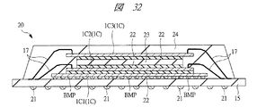
図32は、本実施の形態1の半導体装置の製造方法により製造された半導体装置20の断面図の一例を示している。この半導体装置20は、1つのパッケージ内に所望の機能のシステムが構築されたSIP(System In Package)構成とされている。この半導体装置20を構成するプリント配線基板15の裏面には、複数のバンプ電極21がマトリックス状に配置されている。また、プリント配線基板15の主面上には、複数の薄型のチップ1C1〜1C3(1C)が積層されている。最下層のチップ1C1は、その主面のバンプ電極BMPを介してプリント配線基板15の主面上に実装されている。このチップ1Cの主面には、例えばCPU(Central Processing Unit)やDSP(Digital Signal Processor)等のような論理回路が形成されている。このチップ1Cの裏面上には、ダイアタッチフィルム22を介してチップ1C2が実装されている。チップ1C2の主面には、例えばSRAM(Static Random Access Memory)やフラッシュメモリ等のようなメモリ回路が形成されている。このチップ1C2の主面のパッド1LBは、ワイヤ17を介してプリント配線基板15の主面の電極と電気的に接続されている。このチップ1C2の主面上には、スペーサ23およびダイアタッチフィルム22を介してチップ1C3が実装されている。このチップ1C3には、例えばSRAMやフラッシュメモリ等のようなメモリ回路が形成されており、チップ1C3の主面のパッド1LBは、ワイヤ17を介してプリント配線基板15の主面の電極と電気的に接続されている。このようなチップ1C1〜1C3およびワイヤ17は、例えばエポキシ樹脂からなる封止体24により封止されている。上記した本実施の形態1の半導体装置の製造方法によれば、図32のようなチップ1C1〜1C3の多段積層ができ、SIP構成を有する半導体装置20の薄型化を実現することができる。また、SIP構成を有する半導体装置20の信頼性を向上させることができる。
FIG. 32 shows an example of a cross-sectional view of the
(実施の形態2)
図33は本実施の形態2の半導体装置の製造工程中のウエハ1Wの切断領域CRの拡大平面図を示している。本実施の形態2では、パッド1LBtおよび前記アライメントターゲットAm(以下、パッド1LBt等という)の中心線がステルスダイシング時のレーザ光LBが照射される切断線CLからずれて配置されている。図33では、パッド1BLtが切断線CLを跨がずに切断線CLの上下に互いに斜め方向の位置になるように配置されている。なお、パッド1LBtと電気的に接続されるTEG用の素子や配線1L1も切断線CLを跨がないように上下に分離されて配置されている。
(Embodiment 2)
FIG. 33 shows an enlarged plan view of the cutting region CR of the
このようなパッド1LBt等の配置によれば、パッド1LBt等は、ウエハ1Wの切断時に既に分割されており切断されることがないので、ひげ状の導体異物の発生を防止できる。このため、薄型の半導体装置の信頼性をさらに向上させることができる。また、パッド1LBt等をステルスダイシング時のレーザ光LBが当たらないように離れて配置することにより、レーザ光LBをウエハ1Wの主面から照射することもできる。
According to such an arrangement of the pads 1LBt and the like, since the pads 1LBt and the like are already divided when the
図34および図35は、本実施の形態2の変形例を示している。図34では、パッド1LBtが切断線CLを中心に上下対称に配置されている。また、図33および図34では、切断線CLが切断領域CRの幅方向のほぼ中心を通過するのに対して、図35では、切断線CLが切断領域CRの幅方向中心からずれて配置されている。この場合、図33および図34の場合と切断領域CRの幅の寸法は同じでも、図5、図7、図33および図34の場合よりもパッド1LBtの面積を大きくできるので、上記テスト工程101においてパッド1LBtにプローブを当て易くすることができる。 34 and 35 show a modification of the second embodiment. In FIG. 34, the pads 1LBt are arranged vertically symmetrically about the cutting line CL. In FIGS. 33 and 34, the cutting line CL passes through substantially the center in the width direction of the cutting region CR, whereas in FIG. 35, the cutting line CL is arranged so as to be shifted from the center in the width direction of the cutting region CR. ing. In this case, even if the width dimension of the cutting region CR is the same as in FIGS. 33 and 34, the area of the pad 1LBt can be made larger than in the case of FIGS. 5, 7, 33, and 34. The probe can be easily applied to the pad 1LBt.
(実施の形態3)
本実施の形態3では、チップ1Cの裏面にダイアタッチフィルム22を設ける場合について説明する。
(Embodiment 3)
In the third embodiment, a case where the die attach
まず、前工程100からステルスダイシングのレーザ光LBの照射工程102B2までは前記実施の形態1と同じである。続いて、図36に示すように、ウエハ1Wの裏面にダイアタッチフィルム22を貼り付ける。ダイアタッチフィルム22は、引き伸ばすことで切断できるくらいの柔らかい材料であり、例えばポリイミドである。その後、前記実施の形態1と同様に図37に示すように、治具3を載置台10に載せた状態で、リング3bを矢印Aに示す方向に押し下げテープ3aを矢印Bに示すように引き伸ばしテープ3aの伸びる力により、ウエハ1Wを改質層を形成しない状態で切断するために要する力よりも小さな力で切断し、個々のチップ1Cに分割する。この時に、ダイアタッチフィルム22も一緒に切断される。このようにして、裏面にダイアタッチフィルム22を設けたチップ1Cを用意することができる。
First, the steps from the
(実施の形態4)
本実施の形態4では、一般的な後工程への適用例を図38の半導体装置の製造装置のフロー図に沿って説明する。
(Embodiment 4)
In the fourth embodiment, an application example to a general post-process will be described with reference to the flow chart of the semiconductor device manufacturing apparatus in FIG.
まず、前記実施の形態1と同様に、前工程200から裏面研磨工程202A4を行う。本実施の形態4では、裏面研磨工程202A4後のウエハ1Wの厚さは、前記実施の形態1の場合よりも厚く、例えば220〜280μm程度とされている。また、裏面研削および裏面研磨に際してウエハ1Wの主面に貼り付ける保護テープについては、リングを設けていない一般的なものを用いている。続いて、前記実施の形態1と同様に、ウエハ1Wの主面のパターン(切断領域)を認識し(工程202B1)、レーザ光LBをウエハ1Wの裏面から照射し、ウエハ1Wの内部に改質層PLを形成した後(工程202B2)、図39に示すようにウエハ1Wをダイシング用の治具27に収めた後(工程202B4)、ウエハ1Wの主面に貼り付けた保護テープを剥離する。治具27は、テープ27aとその主面の外周に貼り付けられた剛性を持つリング27bとを有している。テープ27aは、テープベース27a1と、その主面の接着層27a2とを有している。テープ27aの主面には、接着層27a2によりウエハ1Wの裏面が貼り付けられている。すなわち、ウエハ1Wはその主面を上に向けた状態でテープ27aに貼り付けられている。その後、前記実施の形態1と同様に図40に示すように、治具27を載置台10に載せた状態で、リング27bを矢印Aに示す方向に押し下げテープ27aを矢印Bに示すように引き伸ばしテープ27aの伸びる力により、ウエハ1Wを比較的小さな力で切断し、個々のチップ1Cに分割する。本実施の形態4においても、ウエハ1Wの切断領域CRに配置されているパッド1LBt等に図5に示したように溝Sが設けられているため、パッド1LBt等をきれいな形状で切断できるので、ひげ状の導体異物の発生を低減できる。これ以降は、前記実施の形態1と同じなので説明を省略する。なお、ダイアタッチフィルム22を持つ製品を製造する場合には、工程202B4において、予めテープ27aの主面(ウエハ1Wの裏面の対向面)にダイアタッチフィルム22が貼り付けられたものを使用し、ウエハ1Wの裏面をダイアタッチフィルム22を介してテープ27aに貼り付けるようにすると良い。この場合のダイアタッチフィルム22の切断は、前記実施の形態3と同じである。
First, as in the first embodiment, the back surface polishing step 202A4 is performed from the
以上、本発明者によってなされた発明を実施の形態に基づき具体的に説明したが、本発明は前記実施の形態に限定されるものではなく、その要旨を逸脱しない範囲で種々変更可能であることはいうまでもない。 As mentioned above, the invention made by the present inventor has been specifically described based on the embodiment. However, the present invention is not limited to the embodiment, and various modifications can be made without departing from the scope of the invention. Needless to say.
例えばTEGやアライメント用の金属パターン(パッド1LBtやアライメントターゲットAm)をチップの領域内の空き領域(例えば角部や外周近傍)に設け、その金属パターンを切断領域に設けないようにしても良い。これにより、前記実施の形態1等と同様の効果を得ることができる。 For example, a metal pattern for TEG or alignment (pad 1LBt or alignment target Am) may be provided in a vacant area (for example, near a corner or outer periphery) in the chip area, and the metal pattern may not be provided in the cutting area. Thereby, the same effect as the first embodiment can be obtained.
以上の説明では主として本発明者によってなされた発明をその背景となった利用分野である半導体装置の製造方法に適用した場合について説明したが、それに限定されるものではなく種々適用可能であり、例えばマイクロマシンの製造方法にも適用できる。 In the above description, the case where the invention made mainly by the present inventor is applied to the method of manufacturing a semiconductor device which is a field of use as the background has been described. However, the present invention is not limited to this and can be applied in various ways. It can also be applied to a micromachine manufacturing method.
本発明は、半導体装置の製造業に適用できる。 The present invention can be applied to the semiconductor device manufacturing industry.
1W 半導体ウエハ
1C 半導体チップ
1S 半導体基板
1L 配線層
1Li 層間絶縁膜
1L1,1L2 配線
1LB ボンディングパッド
1LBt テスト用のボンディングパッド(金属パターン)
1Lp 保護膜
2 開口部
3 治具
3a テープ
3a1 テープベース
3a2 接着層
3b リング(枠体)
3b1,3b2 切り欠き部
4 吸着ステージ
5a レーザ変位計
5b 赤外線カメラ
6 研削研磨工具
7 吸着ステージ
9 レーザ発生部
10 載置台
11 押上ピン
12 コレット
13 多突起吸着駒
15 プリント配線基板
16 接着材
17 ボンディングワイヤ
20 半導体装置
21 バンプ電極
22 ダイアタッチフィルム
23 スペーサ
24 封止体
27 治具
27a テープ
27a1 テープベース
27a2 接着層
27b リング
N ノッチ
Am アライメントターゲット(金属パターン)
S 溝
LB レーザ光(エネルギービーム)
PL 改質層
1
3b1, 3b2
S Groove LB Laser light (energy beam)
PL modified layer
Claims (9)
(a)複数のチップ領域と、前記複数のチップ領域のうちの互いに隣り合うチップ領域間に設けられた切断領域とを備えた半導体ウエハを準備する工程;
(b)前記(a)工程の後、前記半導体ウエハにテープを貼り付ける工程;
(c)前記(b)工程の後、前記半導体ウエハの前記切断領域に形成された金属パターンを認識する工程;
(d)前記(c)工程の後、前記半導体ウエハの内部に集光点を合わせ、前記切断領域にレーザを照射し、前記切断領域における前記半導体ウエハの前記内部に改質層を形成する工程;
(e)前記(d)工程の後、前記テープを引き伸ばすことにより、前記改質層を起点として前記半導体ウエハを分割する工程;
ここで、
前記(d)工程では、平面視において前記金属パターンと重ならないように、前記切断領域に沿ってレーザを照射し、平面視において前記金属パターンと重ならない位置に前記改質層を形成する。 A method for manufacturing a semiconductor device comprising the following steps:
(A) preparing a semiconductor wafer comprising a plurality of chip regions and a cutting region provided between adjacent chip regions of the plurality of chip regions;
( B ) A step of attaching a tape to the semiconductor wafer after the step (a) ;
( C ) After the step (b), a step of recognizing a metal pattern formed in the cutting region of the semiconductor wafer ;
After; (d) (c) step, the combined internal focal point of the semiconductor wafer, wherein the laser is irradiated to the cutting area, the step of forming the modified layer on the inside of the semiconductor wafer in the cutting region ;
(E) after the step (d), by stretching the tape, as engineering to split the semiconductor wafer the modified layer as a starting point;
here,
In the step (d), a laser is irradiated along the cutting region so as not to overlap the metal pattern in plan view, and the modified layer is formed at a position not overlapping the metal pattern in plan view.
前記半導体ウエハは、主面と、前記主面とは反対側の裏面とを有し、
前記(b)工程の後、かつ、前記(c)工程の前に、前記テープに前記半導体ウエハの前記主面を貼り付けた状態で、前記半導体ウエハの前記裏面を研削する工程を有することを特徴とする半導体装置の製造方法。 In the manufacturing method of the semiconductor device according to claim 1,
The semiconductor wafer has a main surface and a back surface opposite to the main surface,
After the step (b), and, prior to step (c), in a state where the pasted main surface of the semiconductor wafer prior to Kite-loop, the step of grinding the back surface of the semiconductor wafer A method for manufacturing a semiconductor device, comprising:
前記半導体ウエハを研削した後に、前記半導体ウエハを研磨することを特徴とする半導体装置の製造方法。 The method of manufacturing a semiconductor device according to claim 2.
A method of manufacturing a semiconductor device, comprising polishing the semiconductor wafer after grinding the semiconductor wafer.
前記半導体ウエハを研磨した後の前記半導体ウエハの厚さは、100μmまたは100μmより薄いことを特徴とする半導体装置の製造方法。 In the manufacturing method of the semiconductor device according to claim 3,
A method of manufacturing a semiconductor device, wherein the thickness of the semiconductor wafer after polishing the semiconductor wafer is 100 μm or less than 100 μm.
前記研磨する工程は、研磨パッドを用いて行われることを特徴とする半導体装置の製造方法。 In the manufacturing method of the semiconductor device according to claim 3,
The method of manufacturing a semiconductor device, wherein the polishing step is performed using a polishing pad.
前記研磨する工程は、エッチング法により行われることを特徴とする半導体装置の製造方法。 In the manufacturing method of the semiconductor device according to claim 3,
The method of manufacturing a semiconductor device, wherein the polishing step is performed by an etching method.
前記金属パターンは、前記切断領域の幅方向において、中心からずれて配置されていることを特徴とする半導体装置の製造方法。 In the manufacturing method of the semiconductor device according to claim 1,
The method of manufacturing a semiconductor device, wherein the metal pattern is arranged so as to be shifted from a center in a width direction of the cutting region.
前記テープには、枠体が貼り付けられており、
前記(b)工程では、平面視において前記枠体の内側に前記半導体ウエハが位置するように、前記半導体ウエハに前記テープを貼り付けることを特徴とする半導体装置の製造方法。 In the manufacturing method of the semiconductor device according to claim 1,
A frame is affixed to the tape,
In the step (b), the tape is attached to the semiconductor wafer so that the semiconductor wafer is positioned inside the frame in a plan view .
前記半導体ウエハの主面は、前記テープの主面に形成された接着層を介して貼り付けられていることを特徴とする半導体装置の製造方法。 The method of manufacturing a semiconductor device according to claim 8.
A method for manufacturing a semiconductor device, wherein the main surface of the semiconductor wafer is attached via an adhesive layer formed on the main surface of the tape.
Priority Applications (1)
| Application Number | Priority Date | Filing Date | Title |
|---|---|---|---|
| JP2004155881A JP4769429B2 (en) | 2004-05-26 | 2004-05-26 | Manufacturing method of semiconductor device |
Applications Claiming Priority (1)
| Application Number | Priority Date | Filing Date | Title |
|---|---|---|---|
| JP2004155881A JP4769429B2 (en) | 2004-05-26 | 2004-05-26 | Manufacturing method of semiconductor device |
Publications (3)
| Publication Number | Publication Date |
|---|---|
| JP2005340423A JP2005340423A (en) | 2005-12-08 |
| JP2005340423A5 JP2005340423A5 (en) | 2007-07-05 |
| JP4769429B2 true JP4769429B2 (en) | 2011-09-07 |
Family
ID=35493652
Family Applications (1)
| Application Number | Title | Priority Date | Filing Date |
|---|---|---|---|
| JP2004155881A Expired - Fee Related JP4769429B2 (en) | 2004-05-26 | 2004-05-26 | Manufacturing method of semiconductor device |
Country Status (1)
| Country | Link |
|---|---|
| JP (1) | JP4769429B2 (en) |
Families Citing this family (30)
| Publication number | Priority date | Publication date | Assignee | Title |
|---|---|---|---|---|
| JP4833657B2 (en) * | 2005-12-19 | 2011-12-07 | 株式会社ディスコ | Wafer division method |
| JP2007207871A (en) * | 2006-01-31 | 2007-08-16 | Denso Corp | Semiconductor wafer equipped witt plural semiconductor devices |
| JP2007250598A (en) * | 2006-03-14 | 2007-09-27 | Renesas Technology Corp | Process for manufacturing semiconductor device |
| JP4480728B2 (en) | 2006-06-09 | 2010-06-16 | パナソニック株式会社 | Method for manufacturing MEMS microphone |
| JP4910746B2 (en) * | 2007-02-13 | 2012-04-04 | セイコーエプソン株式会社 | Substrate dividing method and droplet discharge head manufacturing method. |
| JP4835583B2 (en) * | 2007-11-26 | 2011-12-14 | パナソニック株式会社 | Manufacturing method of semiconductor device with die attach film |
| JP5163358B2 (en) * | 2008-03-26 | 2013-03-13 | 日立化成株式会社 | Semiconductor wafer dicing method |
| JP5217557B2 (en) * | 2008-03-27 | 2013-06-19 | パナソニック株式会社 | Manufacturing method of electronic parts |
| US8017942B2 (en) | 2008-11-25 | 2011-09-13 | Infineon Technologies Ag | Semiconductor device and method |
| JP2010177277A (en) * | 2009-01-27 | 2010-08-12 | Tokyo Seimitsu Co Ltd | Laser dicing method and laser dicing device |
| JP5401301B2 (en) | 2009-12-28 | 2014-01-29 | ルネサスエレクトロニクス株式会社 | Semiconductor device manufacturing method and semiconductor device |
| JP2012089709A (en) * | 2010-10-20 | 2012-05-10 | Disco Abrasive Syst Ltd | Method for dividing workpiece |
| JP2012134333A (en) * | 2010-12-22 | 2012-07-12 | Disco Abrasive Syst Ltd | Method for measurement |
| US8809120B2 (en) | 2011-02-17 | 2014-08-19 | Infineon Technologies Ag | Method of dicing a wafer |
| JP2012070004A (en) * | 2011-12-21 | 2012-04-05 | Mitsumi Electric Co Ltd | Manufacturing method of semiconductor device |
| US9040389B2 (en) | 2012-10-09 | 2015-05-26 | Infineon Technologies Ag | Singulation processes |
| JP2015056605A (en) | 2013-09-13 | 2015-03-23 | ルネサスエレクトロニクス株式会社 | Method for manufacturing semiconductor device |
| JP5770245B2 (en) * | 2013-10-28 | 2015-08-26 | ルネサスエレクトロニクス株式会社 | Semiconductor device |
| JP5906265B2 (en) * | 2014-03-03 | 2016-04-20 | 株式会社ディスコ | Wafer division method |
| JP6633447B2 (en) * | 2016-04-27 | 2020-01-22 | 株式会社ディスコ | Wafer processing method |
| JP6633446B2 (en) * | 2016-04-27 | 2020-01-22 | 株式会社ディスコ | Wafer processing method |
| JP2018074083A (en) * | 2016-11-02 | 2018-05-10 | 株式会社ディスコ | Processing method of wafer |
| KR102399356B1 (en) * | 2017-03-10 | 2022-05-19 | 삼성전자주식회사 | Substrate, method of sawing substrate, and semiconductor device |
| JP6888809B2 (en) * | 2017-03-30 | 2021-06-16 | 三星ダイヤモンド工業株式会社 | Brittle material substrate with metal film Dividing method and dividing device |
| JP6903532B2 (en) * | 2017-09-20 | 2021-07-14 | キオクシア株式会社 | Semiconductor devices and their manufacturing methods |
| JP7049941B2 (en) * | 2018-06-22 | 2022-04-07 | 株式会社ディスコ | Wafer processing method |
| JP7401183B2 (en) * | 2018-08-07 | 2023-12-19 | 株式会社ディスコ | Wafer processing method |
| KR102653165B1 (en) * | 2018-11-22 | 2024-04-01 | 삼성전자주식회사 | Semiconductor device, semiconductor chip and method of sawing a semiconductor substrate |
| JP7459490B2 (en) | 2019-11-28 | 2024-04-02 | 株式会社ソシオネクスト | Semiconductor wafers and semiconductor devices |
| CN113972143A (en) * | 2021-10-18 | 2022-01-25 | 长鑫存储技术有限公司 | Bonding method of semiconductor structure and semiconductor device |
Family Cites Families (8)
| Publication number | Priority date | Publication date | Assignee | Title |
|---|---|---|---|---|
| JP2000216123A (en) * | 1999-01-22 | 2000-08-04 | Okamoto Machine Tool Works Ltd | Back surface grinding of wafer and dicing method |
| JP3368876B2 (en) * | 1999-11-05 | 2003-01-20 | 株式会社東京精密 | Semiconductor chip manufacturing method |
| JP3339485B2 (en) * | 2000-01-24 | 2002-10-28 | 日本電気株式会社 | Semiconductor device |
| JP2002093750A (en) * | 2000-09-13 | 2002-03-29 | Toshiba Microelectronics Corp | Semiconductor device |
| JP3624909B2 (en) * | 2002-03-12 | 2005-03-02 | 浜松ホトニクス株式会社 | Laser processing method |
| JP2004079746A (en) * | 2002-08-16 | 2004-03-11 | Tokyo Seimitsu Co Ltd | Method of manufacturing chip |
| JP2004111601A (en) * | 2002-09-18 | 2004-04-08 | Tokyo Seimitsu Co Ltd | Die bonder |
| JP3825753B2 (en) * | 2003-01-14 | 2006-09-27 | 株式会社東芝 | Manufacturing method of semiconductor device |
-
2004
- 2004-05-26 JP JP2004155881A patent/JP4769429B2/en not_active Expired - Fee Related
Also Published As
| Publication number | Publication date |
|---|---|
| JP2005340423A (en) | 2005-12-08 |
Similar Documents
| Publication | Publication Date | Title |
|---|---|---|
| JP4769429B2 (en) | Manufacturing method of semiconductor device | |
| JP4796588B2 (en) | Manufacturing method of semiconductor device | |
| JP2005332982A (en) | Method for manufacturing semiconductor apparatus | |
| JP5608521B2 (en) | Semiconductor wafer dividing method, semiconductor chip and semiconductor device | |
| JP3831287B2 (en) | Manufacturing method of semiconductor device | |
| US6841454B2 (en) | Chip-like electronic components, a method of manufacturing the same, a pseudo wafer therefor and a method of manufacturing thereof | |
| JP2007048958A (en) | Semiconductor device and manufacturing method thereof | |
| US7285864B2 (en) | Stack MCP | |
| US20070275543A1 (en) | Manufacturing method of a semiconductor device | |
| US9059225B2 (en) | Semiconductor device and the method of manufacturing the same | |
| JP5798834B2 (en) | Manufacturing method of semiconductor device | |
| JP5352624B2 (en) | Manufacturing method of semiconductor device | |
| KR20040036654A (en) | Fabrication method of semiconductor integrated circuit device | |
| JP2011181822A (en) | Method of fabricating semiconductor device | |
| US10490531B2 (en) | Manufacturing method of semiconductor device and semiconductor device | |
| JP2013080972A (en) | Method of manufacturing semiconductor device | |
| TWI381485B (en) | Semiconductor device manufacturing method and semiconductor device | |
| JP2014146829A (en) | Semiconductor chip and semiconductor device | |
| JP2020136650A (en) | Chip transfer plate, semiconductor chip stacking method, and semiconductor device manufacturing method | |
| WO2021084902A1 (en) | Method for manufacturing chip-mounted substrate, and substrate processing device | |
| JP5297491B2 (en) | Semiconductor device | |
| JP2005340431A (en) | Method for manufacturing semiconductor device | |
| JP2007266421A (en) | Semiconductor device and manufacturing method thereof | |
| WO2007049356A1 (en) | Semiconductor device and method for manufacturing same | |
| JP2012124300A (en) | Wafer breaking method and wafer breaking device |
Legal Events
| Date | Code | Title | Description |
|---|---|---|---|
| A521 | Request for written amendment filed |
Free format text: JAPANESE INTERMEDIATE CODE: A523 Effective date: 20070522 |
|
| A621 | Written request for application examination |
Free format text: JAPANESE INTERMEDIATE CODE: A621 Effective date: 20070522 |
|
| A977 | Report on retrieval |
Free format text: JAPANESE INTERMEDIATE CODE: A971007 Effective date: 20100121 |
|
| A711 | Notification of change in applicant |
Free format text: JAPANESE INTERMEDIATE CODE: A712 Effective date: 20100528 |
|
| A131 | Notification of reasons for refusal |
Free format text: JAPANESE INTERMEDIATE CODE: A131 Effective date: 20100831 |
|
| A521 | Request for written amendment filed |
Free format text: JAPANESE INTERMEDIATE CODE: A523 Effective date: 20101101 |
|
| A01 | Written decision to grant a patent or to grant a registration (utility model) |
Free format text: JAPANESE INTERMEDIATE CODE: A01 Effective date: 20110531 |
|
| A01 | Written decision to grant a patent or to grant a registration (utility model) |
Free format text: JAPANESE INTERMEDIATE CODE: A01 |
|
| A61 | First payment of annual fees (during grant procedure) |
Free format text: JAPANESE INTERMEDIATE CODE: A61 Effective date: 20110620 |
|
| R150 | Certificate of patent or registration of utility model |
Free format text: JAPANESE INTERMEDIATE CODE: R150 |
|
| FPAY | Renewal fee payment (event date is renewal date of database) |
Free format text: PAYMENT UNTIL: 20140624 Year of fee payment: 3 |
|
| S531 | Written request for registration of change of domicile |
Free format text: JAPANESE INTERMEDIATE CODE: R313531 |
|
| R350 | Written notification of registration of transfer |
Free format text: JAPANESE INTERMEDIATE CODE: R350 |
|
| LAPS | Cancellation because of no payment of annual fees |