JP4715149B2 - Method for manufacturing thin film semiconductor device - Google Patents
Method for manufacturing thin film semiconductor device Download PDFInfo
- Publication number
- JP4715149B2 JP4715149B2 JP2004286325A JP2004286325A JP4715149B2 JP 4715149 B2 JP4715149 B2 JP 4715149B2 JP 2004286325 A JP2004286325 A JP 2004286325A JP 2004286325 A JP2004286325 A JP 2004286325A JP 4715149 B2 JP4715149 B2 JP 4715149B2
- Authority
- JP
- Japan
- Prior art keywords
- thin film
- semiconductor thin
- irradiation
- semiconductor
- laser beam
- Prior art date
- Legal status (The legal status is an assumption and is not a legal conclusion. Google has not performed a legal analysis and makes no representation as to the accuracy of the status listed.)
- Active
Links
Images


Description
本発明は薄膜半導体装置の製造方法および薄膜半導体装置に関し、特には半導体薄膜の結晶化のためのアニール工程を有する薄膜半導体装置の製造方法およびこれによって得られる薄膜半導体装置に関する。 The present invention relates to a method for manufacturing a thin film semiconductor device and a thin film semiconductor device , and more particularly to a method for manufacturing a thin film semiconductor device having an annealing process for crystallization of a semiconductor thin film and a thin film semiconductor device obtained thereby .
液晶表示装置や有機EL表示装置のようなフラット型の表示装置においては、複数画素のアクティブマトリックス表示を行うためのスイッチング素子として、薄膜トランジスタ(thin film transistor:TFT)が用いられている。 In a flat display device such as a liquid crystal display device or an organic EL display device, a thin film transistor (TFT) is used as a switching element for performing an active matrix display of a plurality of pixels.
このような表示装置における画素スイッチング素子用の薄膜半導体装置(薄膜トランジスタ)としては、非晶質シリコンからなる半導体薄膜をチャネル部およびソース・ドレインとした、いわゆる非晶質シリコンTFTが用いられている。このような非晶質シリコンTFTは、素子間の特性バラツキが少ない点において、表示装置用のスイッチング素子に適している。また、熱分解ではなくプラズマ分解のCVD法によって非晶質シリコンからなる半導体薄膜を成膜することにより、低温プロセスでの製造が可能になることから、基板として石英、単結晶シリコンなどの高耐熱性ではあるが高価な基板を用いる必要がなくなり、プラスチック基板などを用いることによりフラット型の表示装置の低コスト化を図ることができる。 As a thin film semiconductor device (thin film transistor) for a pixel switching element in such a display device, a so-called amorphous silicon TFT using a semiconductor thin film made of amorphous silicon as a channel portion and a source / drain is used. Such an amorphous silicon TFT is suitable as a switching element for a display device in that there is little characteristic variation between elements. In addition, by forming a semiconductor thin film made of amorphous silicon by CVD method using plasma decomposition instead of thermal decomposition, it becomes possible to manufacture at a low temperature process. However, it is not necessary to use an expensive substrate, and the cost of a flat display device can be reduced by using a plastic substrate or the like.
しかしながら、非晶質シリコンTFTでは、非晶質シリコンに不純物をドーピングしてなるソース・ドレインにおいての活性化効率を期待できず、実効的なキャリア移動度およびOn/Off電流比が小さい。このことが、より高精細で高機能な表示装置用のスイッチング素子として、非晶質シリコンTFTを用いることを阻害する要因となっている。 However, in an amorphous silicon TFT, the activation efficiency in the source / drain formed by doping impurities into amorphous silicon cannot be expected, and the effective carrier mobility and On / Off current ratio are small. This is a factor that hinders the use of amorphous silicon TFTs as switching elements for display devices with higher definition and higher functionality.
そこで、チャネル部が非晶質シリコンからなり、ソース・ドレインが多結晶シリコンからなる、非晶質−結晶質混成の薄膜トランジスタ(以下、混成薄膜トランジスタと記す)を、低温プロセスにて製造する方法が提案された。この方法は、次の手順で行われる。 Therefore, a method of manufacturing an amorphous-crystalline hybrid thin film transistor (hereinafter referred to as a hybrid thin film transistor) in which the channel portion is made of amorphous silicon and the source / drain is made of polycrystalline silicon is proposed by a low temperature process. It was done. This method is performed in the following procedure.
先ず、基板上に、ゲート電極を形成してこれをゲート絶縁膜で覆う。次いで、プラズマ分解のCVD法によって非晶質シリコンからなる半導体薄膜を成膜し、この上部に窒化シリコンからなるマスクパターンを形成する。そして、このマスクパターンを覆う状態で不純物層を塗布形成し、この不純物層の上方からレーザ光を照射する。この際、1箇所に250mJ/パルスの照射エネルギーで40パルスのレーザ光照射を行う。これにより、マスクパターンから露出している半導体薄膜部分に不純物層内の不純物を拡散させると共にこの部分を結晶化し、半導体薄膜に多結晶シリコンからなるソース・ドレインを形成する。またこの際、マスクパターン下の半導体薄膜部分は非晶質シリコンのまま残り、この部分がチャネル部となる。このようにして得られた混成薄膜トランジスタは、通常の非晶質シリコンTFTと比較して、ソース・ドレインを結晶化したことにより実効的な移動度およびOn/Off電流比が高くなる等、特性が大きく向上するとしている。尚、半導体薄膜の結晶化においては、レーザ光の照射エネルギーの上昇にともない半導体薄膜のシート抵抗が低下するが、照射エネルギー250mJ/ショット程度でシート抵抗が飽和する。このため、半導体薄膜へのレーザ光の照射エネルギーは、最大で250mJ/ショットとしている(下記特許文献1参照)。
First, a gate electrode is formed on a substrate and covered with a gate insulating film. Next, a semiconductor thin film made of amorphous silicon is formed by a plasma decomposition CVD method, and a mask pattern made of silicon nitride is formed thereon. Then, an impurity layer is applied and formed so as to cover the mask pattern, and laser light is irradiated from above the impurity layer. At this time, laser light irradiation of 40 pulses is performed at one place with irradiation energy of 250 mJ / pulse. As a result, impurities in the impurity layer are diffused into the semiconductor thin film portion exposed from the mask pattern, and this portion is crystallized to form a source / drain made of polycrystalline silicon in the semiconductor thin film. At this time, the semiconductor thin film portion under the mask pattern remains amorphous silicon, and this portion becomes a channel portion. The hybrid thin film transistor thus obtained has characteristics such as effective mobility and high On / Off current ratio due to crystallization of the source and drain compared to a normal amorphous silicon TFT. It is said that it will greatly improve. In the crystallization of the semiconductor thin film, the sheet resistance of the semiconductor thin film decreases as the laser beam irradiation energy increases, but the sheet resistance is saturated at an irradiation energy of about 250 mJ / shot. For this reason, the irradiation energy of the laser beam to the semiconductor thin film is set to 250 mJ / shot at the maximum (see
ところで、非晶質シリコンからなる半導体薄膜を低温プロセスによって成膜した場合には、多量の水素を含有したいわゆる水素化非晶質シリコン(a−Si:H)が形成される。このため、レーザ光照射による結晶化アニールの際には、膜中の水素がガス化して膜を破壊する現象(Hydrogen ablation:アブレーション)を起こすことが知られている。そして、「H.Heise et al; Journal of Non-Crystalline Solids 299-302(2002)p.226〜p.230」においては、水素化非晶質シリコン膜(a−Si:H)にレーザ光を照射した場合に、膜が完全にアブレーションしてしまうレーザ光の照射エネルギーは、250mJ/cm2程度であるとされている。これは、上述の非特許文献1に示された、レーザ光の照射エネルギーの上昇にともない半導体薄膜のシート抵抗が低下して飽和する照射エネルギーと一致している。
By the way, when a semiconductor thin film made of amorphous silicon is formed by a low temperature process, so-called hydrogenated amorphous silicon (a-Si: H) containing a large amount of hydrogen is formed. For this reason, it is known that during crystallization annealing by laser light irradiation, hydrogen in the film is gasified to cause a phenomenon (Hydrogen ablation) that destroys the film. In "H. Heise et al; Journal of Non-Crystalline Solids 299-302 (2002) p.226-p.230", laser light is applied to the hydrogenated amorphous silicon film (a-Si: H). The irradiation energy of laser light that completely ablate the film when irradiated is supposed to be about 250 mJ / cm 2 . This coincides with the irradiation energy shown in the above-mentioned Non-Patent
一方、レーザ光照射による結晶化アニールの前処理として、加熱による脱水素処理が施された水素化非晶質シリコン膜においては、レーザ光の照射エネルギー330mJ/cm2までシート抵抗の低下が飽和することはない。 On the other hand, in a hydrogenated amorphous silicon film that has been subjected to dehydrogenation treatment by heating as pretreatment for crystallization annealing by laser light irradiation, the decrease in sheet resistance is saturated up to a laser light irradiation energy of 330 mJ / cm 2. There is nothing.
これらのことを考慮すると、レーザ光照射による半導体薄膜の結晶化においては、活性化効率の向上(シート抵抗の低下)と水素ガスによる膜破壊とがトレードオフの関係にあると言える。 Considering these, it can be said that in the crystallization of a semiconductor thin film by laser light irradiation, there is a trade-off relationship between improvement in activation efficiency (decrease in sheet resistance) and film destruction by hydrogen gas.
したがって、レーザ光照射による半導体薄膜の結晶化において、半導体薄膜のさらなる活性化効率の向上を図るためには、レーザ光照射の前工程として十分な脱水素処理を行えば良いことになる。 Therefore, in crystallization of a semiconductor thin film by laser light irradiation, in order to further improve the activation efficiency of the semiconductor thin film, a sufficient dehydrogenation process may be performed as a pre-process of laser light irradiation.
しかしながら、上述した混成薄膜トランジスタを低温プロセスにて製造する方法に、レーザ光照射による結晶化の前工程として脱水素処理を付加すると、半導体薄膜の全体部分から水素が放出されるため、チャネル部となる領域からもダングリングボンドに終端されている水素が放出されてしまうことになる。これは、混成薄膜トランジスタにおいて、チャネル部におけるキャリア移動度を低下させる要因となる。 However, if a dehydrogenation treatment is added as a pre-crystallization process by laser light irradiation to the above-described method for manufacturing a hybrid thin film transistor by a low-temperature process, hydrogen is released from the entire semiconductor thin film, thereby forming a channel portion. Hydrogen terminated with dangling bonds is also released from the region. This becomes a factor of reducing the carrier mobility in the channel portion in the hybrid thin film transistor.
そこで本発明は、非晶質領域で構成されたチャネル部におけるキャリア移動度が高く、しかも結晶化領域で構成されたソース・ドレインの活性化効率が高い、非晶質−結晶質混成の薄膜トランジスタを、低温プロセスで得ることが可能な薄膜半導体装置の製造方法を提供することを目的とする。 Accordingly, the present invention provides an amorphous-crystalline hybrid thin film transistor that has high carrier mobility in a channel portion formed of an amorphous region and high source / drain activation efficiency formed of a crystallization region. Another object of the present invention is to provide a method of manufacturing a thin film semiconductor device that can be obtained by a low temperature process.
このような目的を達成するための本発明の薄膜半導体装置の製造方法は、次の工程を行うことを特徴としている。先ず第1工程では、基板上に非晶質の半導体薄膜を形成し、さらに当該半導体薄膜上にゲート絶縁膜を介してゲート電極をパターン形成する。次の第2工程では、ゲート電極をマスクにして半導体薄膜に不純物を導入する。その後の第3工程では、ゲート電極をマスクにして半導体薄膜に対してレーザ光を照射する。この際、所定速度で照射位置を移動させながらレーザ光を連続照射する。これにより、半導体薄膜の結晶化と共に、当該半導体薄膜中において水素イオンをガス化膨張させることなく当該レーザ光の照射部から余剰水素を除去する。 In order to achieve such an object, a method for manufacturing a thin film semiconductor device of the present invention is characterized by performing the following steps. In the first step, an amorphous semiconductor thin film is formed on a substrate, and a gate electrode is patterned on the semiconductor thin film via a gate insulating film. In the next second step, impurities are introduced into the semiconductor thin film using the gate electrode as a mask. In the subsequent third step, the semiconductor thin film is irradiated with laser light using the gate electrode as a mask. At this time, the laser beam is continuously irradiated while moving the irradiation position at a predetermined speed. Thereby, together with crystallization of the semiconductor thin film, surplus hydrogen is removed from the laser light irradiation portion without gasifying and expanding hydrogen ions in the semiconductor thin film.
このような製造方法によれば、半導体薄膜を結晶化するための第3工程で、半導体薄膜に対するレーザ光の照射位置を所定速度で移動させながら連続照射することにより、レーザ光の照射部における余剰水素がレーザ光の移動に伴って移動する固液界面において固体側から液体側に拡散しながら半導体薄膜中を移動し続けることになる。つまり、膜中の過剰な水素は膜中を移動してレーザ光の照射部の結晶化領域から除去されるだけであり、最終的にはレーザ光の照射端部に析出する。このため、半導体薄膜中の水素イオンが、レーザ光の照射によって加熱され水素ガスとして膜中において膨張して放出され、これにより膜破壊を起こすことが防止される。したがって、さらに活性化効率の高い結晶化領域からなるソース・ドレインが得られる。 According to such a manufacturing method, in the third step for crystallizing the semiconductor thin film, by continuously irradiating the semiconductor thin film while moving the irradiation position of the laser light at a predetermined speed, the surplus in the laser light irradiation portion is obtained. The hydrogen continues to move in the semiconductor thin film while diffusing from the solid side to the liquid side at the solid-liquid interface where the hydrogen moves as the laser beam moves. In other words, excess hydrogen in the film moves only through the film and is removed from the crystallization region of the laser light irradiation portion, and finally precipitates at the laser light irradiation end. For this reason, hydrogen ions in the semiconductor thin film are heated by laser light irradiation and expanded and discharged as hydrogen gas in the film, thereby preventing film breakdown. Therefore, a source / drain composed of a crystallization region with higher activation efficiency can be obtained.
そして以上のように、レーザ光照射の前処理として脱水素処理を行わなくても、膜破壊を防止しつつレーザ光照射部の結晶化が行われため、当該レーザ光照射においてマスクとなるゲート電極下方の半導体薄膜部分には、水素を含有した状態の非晶質領域がそのまま残される。したがって、キャリア移動度が保たれた非晶質のチャネル部が得られる。 As described above, since the laser beam irradiation portion is crystallized while preventing film destruction without performing dehydrogenation as a pretreatment for laser beam irradiation, the gate electrode serving as a mask in the laser beam irradiation is performed. In the lower semiconductor thin film portion, an amorphous region containing hydrogen is left as it is. Therefore, an amorphous channel portion in which carrier mobility is maintained can be obtained.
以上説明したように本発明の薄膜半導体装置の製造方法によれば、脱水素処理を行うことなく膜破壊のないレーザ光照射による結晶化をゲート電極マスクにして行うことで、非晶質領域で構成されたチャネル部におけるキャリア移動度が高く、しかも結晶化領域で構成されたソース・ドレインの活性化効率が高い、非晶質−結晶質混成の薄膜トランジスタを、低温プロセスで得ることが可能である。
そしてこの結果、上述したように特性の良好な混成薄膜トランジスタを、プラスチック基板上に形成することが可能になり、例えばロール・ツー・ロールでの設備費用を抑えた量産プロセスを実現することができる。
As described above, according to the method for manufacturing a thin film semiconductor device of the present invention, crystallization by laser beam irradiation without film destruction without performing dehydrogenation is performed using a gate electrode mask, so that an amorphous region can be obtained. It is possible to obtain an amorphous-crystalline hybrid thin film transistor having a high carrier mobility in the constituted channel portion and a high activation efficiency of the source / drain constituted by the crystallization region by a low temperature process. .
As a result, it is possible to form a hybrid thin film transistor with good characteristics on a plastic substrate as described above, and to realize a mass production process in which, for example, roll-to-roll equipment costs are suppressed.
以下、本発明の実施の形態を図面に基づいて詳細に説明する。尚、各実施形態においては、薄膜半導体装置として、トップゲート型の薄膜トランジスタを備えた薄膜半導体装置を例示し、その製造方法から順に実施形態を説明する。 Hereinafter, embodiments of the present invention will be described in detail with reference to the drawings. In each embodiment, as the thin film semiconductor device, a thin film semiconductor device including a top gate type thin film transistor is illustrated, and the embodiments are described in order from the manufacturing method.
<第1実施形態>
図1は第1実施形態の薄膜半導体装置の製造方法を示す断面工程図である。ここではこの図1に基づいて第1実施形態の製造方法を説明する。
<First Embodiment>
FIG. 1 is a cross-sectional process diagram illustrating the method of manufacturing the thin film semiconductor device of the first embodiment. Here, the manufacturing method of the first embodiment will be described with reference to FIG.
先ず、図1(1)に示すように、薄膜半導体装置を形成する基板1を用意する。この基板1としては、非晶質基板のガラス、石英、サファイア基板、プラスチック基板、さらにはアルミニウムやステンレス等の金属基板等を用いる。そして、この基板1の一主面上に、当該基板1への熱伝導を防止するための絶縁性のバッファー層3を設ける。尚、基板1およびバッファー層3の詳細な構成については、別項目にて後述する。
First, as shown in FIG. 1A, a
次に、基板1の一主面側上に、バッファー層3を介して非晶質の半導体薄膜5を形成する。ここでは、成膜温度を低く抑えることが可能な成膜方法を採用することとし、例えば一般的なプラスチックの耐熱温度である250℃以下に成膜温度が抑えられる、PE−CVD(plasma enhancement-chemical vapor deposition)法による非晶質シリコンからなる半導体薄膜5の形成を行う。
Next, an amorphous semiconductor
PE−CVD法による半導体薄膜5の形成の一例を示す。
成膜ガスおよび流量:SiH4(10vol%)/H2=50sccm、
成膜雰囲気内圧力 :200mTorr、
基板温度 :130℃、
RFパワー :20W
成膜時間 :6.5分
以上により、膜厚50nmの半導体薄膜5を成膜する。この半導体薄膜5は、多量の水素が含有されたいわゆる水素化非晶質シリコン(a−Si:H)からなる。
An example of formation of the semiconductor
Deposition gas and flow rate: SiH 4 (10 vol%) / H 2 = 50 sccm,
Deposition atmosphere pressure: 200 mTorr,
Substrate temperature: 130 ° C.
RF power: 20W
Film formation time: 6.5 minutes As described above, the semiconductor
尚、半導体薄膜5の形成は、成膜温度を低く抑えられる方法であれば上述したPE−CVD法に限定されることはなく、塗布法によって行っても良い。この場合、ポリシラン化合物を溶媒に混ぜた混合物を、バッファー層3を介して基板1上に塗布成膜し、その後、乾燥、アニールを施すことにより半導体薄膜5を形成する。そして、先のPE−CVD法や、ここで示した塗布法などの成膜温度が低く抑えられた成膜方法では、いずれの場合にも成膜条件により多少の変動はあるが、0.5atoms%〜15atoms%程度の水素を含有した水素化非晶質シリコン(a−Si:H)からなる半導体薄膜5が得られる。
The formation of the semiconductor
次に、半導体薄膜5上にゲート絶縁膜7を形成する。このゲート絶縁膜7は、酸化シリコンからなるもので良く、通常のPE−CVDによる公知の方法で成膜可能であり、この他にも塗布型の絶縁層として公知のSOG等の成膜を行っても良い。
Next, a
次に、ゲート絶縁膜7上にゲート電極9を形成する。ここでは、先ず、スパッタ法または蒸着法により、例えばアルミニウムからなる電極材料層を成膜し、次にリソグラフィー法によってこの電極材料層上にレジストパターンを形成する。その後、このレジストパターンをマスクに用いて電極材料層をエッチングすることにより、ゲート電極9をパターン形成する。尚、ゲート電極9の形成は、このような手順に限定されることはなく、例えば金属微粒子を塗布して印刷する手法であっても良い。
Next, a gate electrode 9 is formed on the
またゲート電極9の形成に続けて、ゲート電極9をマスクに用いてゲート絶縁膜7をパターンエッチングし、ゲート電極9の両脇に半導体薄膜5を露出させる。
Further, following the formation of the gate electrode 9, the
次に、図1(2)に示すように、半導体薄膜5に対して、ゲート電極9をマスクとした自己整合的な不純物導入を行う。この不純物は、この半導体装置5を用いて構成される薄膜トランジスタのソース・ドレインを構成するものである。ここでは、イオンインプラ、プラズマドーピング等公知の手法を用いることができる。またこの他にも、市販の塗布型のドーパント溶液を用いて方法や、LIMPID(Laser-induced Melting of Predeposited Impurity Doping)法を適用しても良い。
Next, as shown in FIG. 1B, self-aligned impurity introduction is performed on the semiconductor
例えば、LIMPID法を適用した不純物導入を行う場合には、先ず、不純物を含むドーピングガスのプラズマに半導体薄膜5を曝す。この際、例えばPE−CVD装置中にドーピングガスとしてPH3(0.5vol%)/H2:20sccmを流し、処理雰囲気内の圧力を475mTorr、基板温度を150℃、RFパワーを20Wに設定し、照射時間3分の処理を施す。これにより、ゲート電極9をマスクとして、半導体薄膜5の露出面上に選択的に不純物イオンを吸着させる。
For example, when introducing impurities using the LIMPID method, first, the semiconductor
以上の後、図1(3),図1(4)に示すように、ゲート電極9をマスクにして半導体薄膜5にレーザ光Lhを照射することにより、レーザ光Lhの照射部を結晶化して結晶化領域Aを形成するとともに、この結晶化領域Aにおける不純物を活性化させるアニール工程を行う。
After the above, as shown in FIGS. 1 (3) and 1 (4), the semiconductor
このアニール工程においては、半導体薄膜5に対するレーザ光Lhの照射位置を、所定の移動速度vtで移動させる。この際、レーザ光Lhの照射は連続照射とする。これにより、半導体薄膜5中において水素イオンをガス化膨張させることなく、当該レーザ光Lhの照射部、すなわち結晶化領域Aから余剰水素を除去する。
In this annealing step, the irradiation position of the laser beam Lh on the semiconductor
ここで、半導体薄膜5に照射するレーザ光Lhの波長は、半導体薄膜5の膜厚とその吸収係数に基づき、半導体薄膜5の表面層のみで吸収されずに深さ方向広範囲にわたって吸収される程度に、比較的吸収係数が小さくなる波長が選択される。すなわち、厚さ50nmの非晶質シリコンからなる半導体薄膜5を例にとると、波長350nm〜470nmのレーザ光Lhが好ましく用いられる。これにより、半導体薄膜5の表面層のみでレーザ光Lhが吸収されて急激に昇温し、膜中に含まれる水素の膨張により半導体薄膜5が破壊されるアブレーションを防止する。
Here, the wavelength of the laser beam Lh applied to the semiconductor
このような波長のレーザ光Lhの発振源としては、例えばGaN系の化合物半導体レーザ発振器、さらにはYAGレーザ発振器が用いられる。 As an oscillation source of the laser beam Lh having such a wavelength, for example, a GaN compound semiconductor laser oscillator, and further a YAG laser oscillator are used.
また、半導体薄膜5に対するレーザ光Lhの照射位置の移動速度vtは、レーザ光Lhの照射によって加熱された半導体薄膜5の熱が基板1に影響を及ぼすことなく放熱されて半導体薄膜5が結晶化する程度に設定される。このため、半導体薄膜5の移動速度vtは、レーザ光Lhの照射エネルギーを考慮した値に設定され、例えば上述した例においてレーザ光のエネルギーが1J/cm2程度である場合、半導体薄膜5に対するレーザ光Lhの照射位置の移動速度vtを0.1m/秒〜10m/秒に設定する。
Further, the moving speed vt of the irradiation position of the laser light Lh with respect to the semiconductor
尚、半導体薄膜5に対するレーザ光Lhの照射位置の移動は相対的でよく、固定されたレーザ光Lhの照射位置に対して半導体薄膜5が形成された基板1側を移動させても良いし、固定された基板1に対してレーザ光Lhの照射位置を移動させても良い。また、基板1とレーザ光Lhの照射位置との両方を移動させても良い。
The movement of the irradiation position of the laser beam Lh with respect to the semiconductor
そして、半導体薄膜5に対するレーザ光Lhの照射スポット径は、溶融した半導体材料の冷却過程における核の生成確率から決められる。すなわち、レーザ光Lhの照射によって溶融した半導体材料部分においては、レーザ光Lhの照射位置の移動によって照射位置がずれた部分から順次冷却が開始される。そして、同時に冷却が開始された位置で、最も速く結晶の核が形成された部分から結晶が成長する。したがって、このときの核生成確率が1event/sec程度であれば、冷却開始部分から一方向に結晶成長が進むため、過剰な水素はレーザーのスキャン方向側一方向に押し出されていくことになる。
And the irradiation spot diameter of the laser beam Lh with respect to the semiconductor
このため、上述した例においては、半導体薄膜5に対するレーザ光Lhの照射スポット径を10μmを越えない範囲とすることで、核生成確率を1event/sec程度に抑えることが好ましい。尚、生産性を考慮すると、照射スポット径はできるだけ大きいことが好まし。このことからすれば、照射スポット径は10μmを越えない範囲でできるだけ大きい値に設定されることとし、生産性を考慮した現実的なスポット径の下限は、1nm程度となる。
For this reason, in the above-described example, it is preferable to suppress the nucleation probability to about 1 event / sec by setting the irradiation spot diameter of the laser beam Lh to the semiconductor
またさらに以上のようなレーザ光Lhは、半導体薄膜5に対して連続照射されるが、これにより、レーザ光Lhの照射部における余剰水素がレーザ光Lhの移動に伴って半導体薄膜5a中を移動し続け、結晶化領域A中から余剰水素が除去されることになる。そして、レーザ光Lhの照射終了端に余剰水素bを析出させる。尚、余剰水素bはボイドの状態で析出する。
Further, the laser beam Lh as described above is continuously irradiated onto the semiconductor
ここで、半導体薄膜5に対するレーザ光Lhの連続照射とは、レーザ光Lhの移動に際して休止無く完全に連続である場合と共に、レーザ光Lhの照射によって溶融した半導体薄膜5部分の凝固が完全に完了しない程度の休止が入る場合を含むこととする。このため、このような条件を満たせば、照射時間よりも短い休止時間が入る場合も連続照射に含まれ、一例として半導体薄膜5部分への100nsの照射時間に対して10〜20ns程度の休止が入る場合も連続照射に含むこととする。尚、照射時間に対する休止時間は、半導体薄膜の材質および膜厚、レーザ光Lhのエネルギー密度、等によって適宜設計される。このような休止時間を入れることにより、レーザ光Lh照射による基板1への熱的影響を抑えることができる。尚、エキシマレーザ光は完全なパルス波であり、300Hz程度のパルス波であれば、25nsの照射時間に対して3300ns程度の休止が入ることになる。このため、エキシマレーザ光では、レーザ光Lhの照射によって溶融した半導体薄膜5部分の凝固が完全した状態で次のパルス照射が行われることになるため、上述したいわゆる「連続照射」を行うことはできない。
Here, the continuous irradiation of the laser beam Lh to the semiconductor
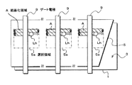
また以上のようなレーザ光Lhの照射は、薄膜トランジスタの形成部分を含む、半導体薄膜5に設定した選択領域5aのみに対して選択的に行うこととする。これにより、選択領域5aへのレーザ光Lhの照射による半導体薄膜5の部分的な発熱がその周囲に放熱され、基板1に対して発熱の影響を及ぼすことを防止する。尚、この選択領域5aとしては、薄膜トランジスタの形成部分以外に、この半導体薄膜5を用いて抵抗素子や容量素子などが形成される領域や、この半導体薄膜5を用いて配線が形成される領域であり、低抵抗化が必要な領域であることとする。
Further, the laser beam Lh irradiation as described above is performed selectively only on the
尚、照射スポット径が、各選択領域5aにおける結晶化領域Aの幅(例えばソース・ドレイン11の幅)に達しない場合には、選択領域5aに対して複数列のレーザ光Lh照射を行うこととする。
When the irradiation spot diameter does not reach the width of the crystallization region A (for example, the width of the source / drain 11) in each
ここで特に、選択領域5aのうち、図示した薄膜トランジスタの形成部分に相当する選択領域5aにおける上記レーザ光Lhの照射は、マスクとなるゲート電極9に重なる位置をレーザ光Lhの照射開始位置とし、この照射開始位置からゲート電極9から選択領域5aの端部方向に向かってレーザ光Lhの照射位置を移動させることとする。
Here, in particular, in the
このため先ず、図1(3)に示すようにゲート電極9に重なる位置をレーザ光Lhの照射開始位置とし、この照射開始位置から選択領域5aの一方側端部に向かってレーザ光Lhの照射位置を所定の移動速度vtで移動させる。その後、図1(4)に示すように、再びゲート電極9に重なる位置をレーザ光Lhの照射開始位置とし、この照射開始位置から選択領域5aの他方側端部に向かってレーザ光Lhの照射位置を所定の移動速度vtで移動させる。
Therefore, first, as shown in FIG. 1 (3), the position overlapping the gate electrode 9 is set as the irradiation start position of the laser beam Lh, and the irradiation of the laser beam Lh from the irradiation start position toward one end of the
以上のようなレーザ光Lhの照射により、半導体薄膜5の選択領域5aを結晶化した結晶化領域Aを形成すると共に、結晶化領域5a中の不純物を活性化させ、さらに結晶化領域A中の余剰水素を除去する脱水素を行う。そして特に、ゲート電極9脇の選択領域5aは、ゲート電極9の両脇の半導体薄膜5部分を結晶化すると共にこの部分の不純物を活性化させ、さらに結晶化領域A中の余剰水素が除去されたソース・ドレイン11となる。また、ゲート電極9の下方には、レーザ光Lhを照射せずに水素化非晶質シリコン(a−Si:H)のまま残したチャネル部13が形成される。そしてこれにより、非晶質−結晶質混成の薄膜トランジスタTFTを得る。さらに、上述したようにゲート電極9に重なる位置をレーザ光Lhの照射開始位置としてレーザ光Lhを移動させることにより、ゲート電極9から離れたソース・ドレイン11の端部に余剰水素bを析出させる。
By irradiation with the laser beam Lh as described above, a crystallized region A is formed by crystallizing the selected
尚、以上のような半導体薄膜5に対するレーザ光Lhの照射は、複数の選択領域5aに対して同時に行う様にすることが好ましい。つまり、図2の平面図に示すように、基板1上に設定配列された複数の選択領域5aに対してレーザ光Lhを同時に多点照射することにより複数の結晶化領域Aを同時に形成することが、生産性を考慮した場合には好ましい方法である。
Note that the irradiation of the laser beam Lh on the semiconductor
このようなレーザ光Lhの多点照射を実現するためには、レーザ光Lhの発振源として半導体レーザ発振器が好適に用いられる。半導体レーザ発振器は、エキシマレーザやYAGレーザなどの他のレーザ発振器と比較して非常に小型であるため、1つの装置内に複数配置が可能であり、かつ連続照射で定格40mWの出力が可能である。尚、このような半導体レーザ発振器を用いたレーザ装置の構成は、別項目にて後述する。 In order to realize such multi-point irradiation of the laser beam Lh, a semiconductor laser oscillator is preferably used as the oscillation source of the laser beam Lh. Semiconductor laser oscillators are extremely small compared to other laser oscillators such as excimer lasers and YAG lasers, so a plurality of semiconductor laser oscillators can be arranged in one device, and a rated output of 40 mW is possible with continuous irradiation. is there. The configuration of the laser apparatus using such a semiconductor laser oscillator will be described later in another item.
ところで、以上のようにレーザ光Lhを所定速度で移動させた連続照射では、図3の平面図に示すように、結晶化領域Aに半導体材料の結晶粒aが形成される。すなわち、結晶化領域Aにおいては、図中矢印で示すレーザ光Lhの移動方向に凸となる三日月形の結晶粒aが、レーザ光Lhの移動方向に沿って配列される。尚、図3においては、レーザ光Lh照射の2列分を図示している。 By the way, in the continuous irradiation in which the laser beam Lh is moved at a predetermined speed as described above, the crystal grains a of the semiconductor material are formed in the crystallization region A as shown in the plan view of FIG. That is, in the crystallization region A, crescent-shaped crystal grains a that are convex in the moving direction of the laser beam Lh indicated by the arrows in the drawing are arranged along the moving direction of the laser beam Lh. In FIG. 3, two rows of laser beam Lh irradiation are shown.
ここで、PE−CVD法で成膜した膜厚50nmの半導体薄膜5a(a−Si:H)に対して、移動速度vt=8.2m/秒で1J/cm2相当のエネルギーでレーザ光Lhを照射したところ、幅800nm×移動方向長さ100nm程度の三日月状の結晶粒aが並んだ多結晶膜が得られることが確認された。またレーザ光の照射終了端には、半導体薄膜5aの結晶領域Aの端部に余剰水素bがボイド状に析出した欠陥が見られた。
Here, with respect to the semiconductor
またレーザ光Lhの照射開始端にもレーザ光の移動と反対方向に凝固が進んだ領域に部分的に同様の欠陥が見られた。したがって、図1(3)、(4)を用いて説明したように、薄膜トランジスタの形成部分では、ゲート電極9に重なる位置をレーザ光Lhの照射開始位置とすることで、非晶質のチャネル部13と結晶化領域Aからなるソース・ドレイン11との境界付近に余剰水素bのボイドが析出することを防止している。
In addition, a similar defect was partially observed in the region where solidification progressed in the direction opposite to the movement of the laser beam at the irradiation start end of the laser beam Lh. Therefore, as described with reference to FIGS. 1 (3) and 1 (4), in the thin film transistor formation portion, the position overlapping the gate electrode 9 is set as the irradiation start position of the laser light Lh, so that an amorphous channel portion is formed. The void of surplus hydrogen b is prevented from precipitating in the vicinity of the boundary between the
そして以上のようなレーザ光照射を行って後には、図4に示すように、半導体薄膜5を、その結晶化領域Aを残して所定形状にパターンエッチングする。またこれにより非晶質−結晶質混成の薄膜トランジスタTFTの素子分離を行う。この場合、図示したように、結晶化領域Aの端部(ソース・ドレイン11の端部)に析出させた余剰水素(b)をエッチングによって除去しても良く、また余剰水素(b)を結晶化領域Aの端部に残しても良い。
After the laser beam irradiation as described above, as shown in FIG. 4, the semiconductor
尚、図4を用いて説明した半導体薄膜5のパターニング工程で、余剰水素(b)を結晶化領域Aの端部に残すようにした場合には、ソース・ドレイン11の外側部分に余剰水素(b)によるバブル状の欠陥が数多く存在している構造の薄膜トランジスタが形成されることになる。
In the patterning process of the semiconductor
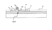
以上のようにして形成された薄膜トランジスタTFTをスイッチング素子として用いた表示装置として、例えば液晶表示装置を作製する場合には、さらに以下の工程を行う。 When a liquid crystal display device is manufactured as a display device using the thin film transistor TFT formed as described above as a switching element, for example, the following steps are further performed.
先ず、図5(1)に示すように、薄膜トランジスタTFTを覆う状態で、基板1上に層間絶縁膜21を形成する。次に、この層間絶縁膜21に薄膜トランジスタTFTのソース・ドレイン11に達する接続孔21aを形成する。そして、この接続孔21aを介してソース・ドレイン11に接続された配線23を、層間絶縁膜21上に形成する。
First, as shown in FIG. 5A, an
次いで、配線23を覆う状態で平坦化絶縁膜25を形成し、配線23に達する接続孔25aを平坦化絶縁膜25に形成する。次に、この接続孔25aと配線23を介してソース・ドレイン11に接続された画素電極27を、平坦化絶縁膜25上に形成する。この画素電極27は、液晶表示装置の表示タイプによって透明電極または反射電極として形成する。尚、図面は1画素の要部断面となっている。
Next, a
その後、ここでの図示は省略したが、画素電極27を覆う配向膜を平坦化絶縁膜上に形成し、駆動基板29を完成させる。
Thereafter, although not shown here, an alignment film covering the
その後、図5(2)に示すように、駆動基板29に対向配置させる対向基板31を用意する。この対向基板31は、透明基板33上に共通電極35を設け、さらにここでの図示を省略した配向膜で共通電極35を覆ってなる。尚、共通電極35は透明電極からなることとする。
Thereafter, as shown in FIG. 5B, a
そして、駆動基板29と対向基板31とを、画素電極27と共通電極35とを向かい合わせた状態で、スペーサ37を介して対向配置する。そして、スペーサ37によって所定間隔に保たれた基板29,31間に液晶相LCを充填封止し、液晶表示装置を完成させる。
Then, the
尚、上記構成の駆動基板29を用いて有機EL表示装置を作製する場合には、駆動基板29に設けられた画素電極を陽極(または陰極)とし、この画素電極上に正孔注入層、発光層、電子輸送層などの必要機能を有する有機層を積層させ、さらに有機層上に共通電極を陰極(または陽極)として形成することとする。
When an organic EL display device is manufactured using the
以上のような製造方法によれば、図1(3)および(4)を用いて説明した半導体薄膜5を結晶化するためのアニール工程で、半導体薄膜5に対するレーザ光Lhの照射位置を所定速度で移動させながら連続照射することにより、レーザLh光の照射部における余剰水素bがレーザ光Lhの移動に伴って半導体薄膜5中を移動し続けることになる。つまり、膜中の水素は膜中を移動してレーザ光の照射部から除去されるのであり、最終的にはレーザ光Lhの照射端部に析出する。このため、半導体薄膜5中の水素が、レーザ光Lhの照射によって加熱され水素ガスとして膜中において膨張して放出され、これにより半導体薄膜5の膜破壊を起こすことが防止される。したがって、さらに活性化効率の高い結晶領域からなるソース・ドレイン11が得られる。
According to the manufacturing method as described above, the irradiation position of the laser beam Lh on the semiconductor
そしてレーザ光Lh照射の前処理として脱水素処理を行わなくても、膜破壊を防止しつつレーザ光Lhの照射部の結晶化が行われため、レーザ光Lhの照射においてマスクとなるゲート電極9下方の半導体薄膜部5分には、水素化非晶質シリコン(a−Si:H)がそのまま残される。したがって、キャリア移動度が保たれた非晶質のチャネル部13が得られる。
Even if the dehydrogenation treatment is not performed as the pretreatment for the laser beam Lh irradiation, the irradiation portion of the laser beam Lh is crystallized while preventing the film destruction, and therefore the gate electrode 9 serving as a mask in the laser beam Lh irradiation is performed. Hydrogenated amorphous silicon (a-Si: H) is left as it is in the lower semiconductor
以上により、非晶質領域で構成されたチャネル部13におけるキャリア移動度が高く、しかも結晶化領域で構成されたソース・ドレイン11の活性化効率が高い、非晶質−結晶質混成の薄膜トランジスタTFTを、低温プロセスで得ることが可能である。
As described above, the amorphous-crystalline hybrid thin film transistor TFT having high carrier mobility in the
またこの結果、基板1としてプラスチック基板を用いることが可能になり、例えばロール・ツー・ロールでの設備費用を抑えた量産プロセスを実現することができる。尚、ロール・ツー・ロールプロセスでの製造を行う場合には、プラスチィックの基板1の厚さは1mm以下であることが望ましい。
As a result, it is possible to use a plastic substrate as the
しかも、上記のアニール工程では、レーザ光Lhの照射部(すなわち結晶化領域A)から余剰水素bが除去されるものの、結晶化領域A内には適量の水素が残存した状態となる。したがって、本アニール工程により、半導体薄膜5における結晶化領域A中の脱水素と水素化処理とを同時に行うことができる。このことから、高機能の膜半導体装置における製造プロセスの簡略化と、これによる生産性の向上を図ることが可能になる。
In addition, in the above annealing process, the excess hydrogen b is removed from the irradiated portion (that is, the crystallization region A) of the laser beam Lh, but an appropriate amount of hydrogen remains in the crystallization region A. Therefore, by this annealing step, dehydrogenation and hydrogenation treatment in the crystallization region A in the semiconductor
<第2実施形態>
図6は第2実施形態の薄膜半導体装置の製造方法を示す断面工程図である。ここではこの図6に基づいて第2実施形態の製造方法を説明する。
<Second Embodiment>
FIG. 6 is a cross-sectional process diagram illustrating the method of manufacturing the thin film semiconductor device of the second embodiment. Here, the manufacturing method of the second embodiment will be described with reference to FIG.
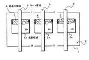
先ず、図6(1)に示すように、第1実施形態において図1(1)を用いて説明したと同様にして、基板1上にバッファー層3を形成する。そして、このバッファー層3上に半導体薄膜パターン5aを形成する。ここでは、この半導体薄膜パターン5aは、第1実施形態で説明した選択領域(5a)と同一形状であることとする。ただし、半導体薄膜パターン5aは、第1実施形態で説明した選択領域(5a)を含む形状であれば良く、選択領域(5a)より大きくても良い。
First, as shown in FIG. 6 (1), the
このような半導体薄膜パターン5aは、成膜温度を低く抑えられる方法で形成されれば良く、第1実施形態と同様にして成膜した半導体薄膜をパターンエッチングして形成しても良い。また、例えば、第1実施形態で説明した塗布法を応用し、必要部分のみに半導体薄膜パターン5aを印刷形成しても良い。したがって、形成された半導体薄膜パターン5aは、第1実施形態の半導体薄膜(5)と同様に、水素を含有した水素化非晶質シリコン(a−Si:H)で構成されることなる。
Such a semiconductor
その後、半導体薄膜パターン5aが形成された基板1の上部にゲート絶縁膜7を介してゲート電極9を形成する。この工程は、第1実施形態において図1(1)を用いて説明したと同様に行って良い。尚、ゲート電極9は、半導体薄膜パターン5aのうち、薄膜トランジスタが形成される半導体薄膜パターン5aの中央を横切るように形成されることとする。
Thereafter, a gate electrode 9 is formed on the
次に、図6(2)に示すように、半導体薄膜パターン5aにゲート電極9をマスクとして自己整合的に不純物を導入する。この工程は、第1実施形態において図1(2)を用いて説明したと同様に行って良い。
Next, as shown in FIG. 6B, impurities are introduced into the semiconductor
その後、図6(3),(4)に示すように、ゲート電極9をマスクにして半導体薄膜パターン5aに対してレーザ光Lhを照射して結晶化するアニール工程を行う。このアニール工程は、第1実施形態において図1(3)および図1(4)を用いて説明したと同様に行い、半導体薄膜パターン5aにレーザ光Lhを照射することにより、レーザ光Lhの照射部を結晶化して結晶化領域Aを形成するとともに、この結晶化領域Aにおける不純物を活性化させ、また結晶化領域A中の余剰水素を除去する脱水素を行う。
Thereafter, as shown in FIGS. 6 (3) and 6 (4), an annealing step is performed in which the semiconductor
そして特に、ゲート電極9脇の半導体薄膜パターン5aにおいては、ゲート電極9の両脇の半導体薄膜パターン5a部分を結晶化すると共にこの部分の不純物を活性化させ、さらに結晶化領域A中の余剰水素が除去されたソース・ドレイン11を形成する。また、ゲート電極9の下方には、レーザ光Lhを照射せずに水素化非晶質シリコン(a−Si:H)のまま残したチャネル部13を形成する。そしてこれにより、非晶質−結晶質混成の薄膜トランジスタTFTを得る。さらに、上述したようにゲート電極9に重なる位置をレーザ光Lhの照射開始位置としてレーザ光Lhを移動させることにより、ゲート電極9から離れたソース・ドレイン11の端部に余剰水素bを析出させる。
In particular, in the semiconductor
またこのアニール工程も、第1実施形態のアニール工程と同様に、複数の結晶化領域Aに対して同時に行う様にすることが好ましい。つまり、図7の平面図に示すように、基板1上に形成された複数の半導体薄膜パターン5aに対して、レーザ光Lhを同時に多点照射することにより複数の結晶化領域Aを同時に形成することが、生産性を考慮した場合には好ましい方法である。ただしこの場合、基板1に対するレーザ光Lh照射による熱的影響を防止するために、半導体パターン5aを外れて、基板1上のバッファー層3にレーザ光Lhが照射されることのないようにする。
Moreover, it is preferable that this annealing process is simultaneously performed for a plurality of crystallized regions A as in the annealing process of the first embodiment. That is, as shown in the plan view of FIG. 7, a plurality of crystallized regions A are simultaneously formed by simultaneously irradiating a plurality of semiconductor
また、以上の様にして形成された非晶質−結晶質混成の薄膜トランジスタTFTをスイッチング素子として用いた表示装置として、例えば液晶表示装置を作製する場合には、第1実施形態で図5を用いて説明したと同様の工程を行う。 When a liquid crystal display device is manufactured as a display device using the amorphous-crystalline hybrid thin film transistor TFT formed as described above as a switching element, for example, FIG. 5 is used in the first embodiment. The same process as described above is performed.
以上のような第2実施形態の製造方法であっても、図6(3)、(4)を用いて説明した半導体薄膜パターン5aを結晶化するためのアニール工程を、第1実施形態のアニール工程と同様に行うことで、製造プロセスにおいての基板1に対する熱的影響を低く抑えることが可能になり、第1実施形態と同様の効果を得ることができる。
Even in the manufacturing method of the second embodiment as described above, the annealing step for crystallizing the semiconductor
<基板>
次に、以上の第1実施形態および第2実施形態で代表される本発明の薄膜半導体装置の製造方法に用いられる基板1の構成を説明する。
<Board>
Next, the configuration of the
上述したように、本発明の薄膜半導体装置の製造方法では、アニール工程での基板に対する熱的影響が低く抑えられるため、基板として用いられる材料に対して特に高い耐熱性が求められることはない。このため、基板としては、非晶質基板のガラス、石英、サファイア基板、プラスチック基板、さらにはアルミニウムおよびステンレスのような金属基板等、多様な材質が用いられる。 As described above, in the method of manufacturing a thin film semiconductor device according to the present invention, the thermal influence on the substrate in the annealing process can be suppressed to a low level, so that a particularly high heat resistance is not required for the material used as the substrate. For this reason, various materials such as an amorphous substrate glass, quartz, sapphire substrate, plastic substrate, and a metal substrate such as aluminum and stainless steel are used as the substrate.
このうち、金属基板を用いる場合には、金属基板における薄膜半導体装置の形成面に、無機材料からなる絶縁性のバッファー層を形成し、これを基板1とする。バッファー層3としては、珪素酸化物や、珪素窒化物、珪素炭化物の他、Ti,Al,Zr,Hf等の酸化膜を用いても構わない。これらのバッファー層3の形成は、CVD、スパッタ、および蒸着等の公知の真空成膜技術によって行うことができる。また、バッファー層としては、無機系SOG膜や有機系SOG等の層間絶縁膜等として通常使用される絶縁層を用いることもできる。さらに金属膜の陽極酸化で形成される誘電体膜や、ゾルゲル法やMOD(Metal Organic Deposition)法等の公知の技術で成膜された膜であっても良い。
Among these, in the case of using a metal substrate, an insulating buffer layer made of an inorganic material is formed on the formation surface of the thin film semiconductor device on the metal substrate, and this is used as the
また、プラスチック基板を用いる場合には、上述した薄膜半導体装置の製造をロール・ツー・ロールプロセスで行うことが可能である。この場合、プラスチィックの基板1の厚さは1mm以下であることが望ましい。
In the case of using a plastic substrate, the above-described thin film semiconductor device can be manufactured by a roll-to-roll process. In this case, the thickness of the
プラスチック基板を構成する有機材料としては、PET(ポリエチレンテレフタレート)、ポリエチレンナフタレートあるいはポリカーボネートなどのポリエステル類、ポリプロピレンなどのポリオレフィン類、ポリフェニリンスルフィドなどのポリフェニリンスルフィド類、ポリアミド類、芳香族ポリアミド類、ポリエーテルケトン類またはポリイミド類、アクリル系樹脂、PMMA(ポリメタクリル酸メチル)などの高分子材料を用いることができる。この中でも特に、ポリエチレンテレフタレート、アセテート、ポリフェニリンスルフィド、ポリカーボネート、PES(ポリエーテルサルフォン),ポリスチレン,ナイロン,ポリプロピレン,ポリ塩化ビニル,アクリル系樹脂、PMMAなどの汎用的なプラスチック基板を好適に用いることができる。 Organic materials constituting the plastic substrate include PET (polyethylene terephthalate), polyesters such as polyethylene naphthalate or polycarbonate, polyolefins such as polypropylene, polyphenyline sulfides such as polyphenylin sulfide, polyamides, and aromatic polyamides. Polymer materials such as polyketones, polyether ketones or polyimides, acrylic resins, and PMMA (polymethyl methacrylate) can be used. Of these, general-purpose plastic substrates such as polyethylene terephthalate, acetate, polyphenylin sulfide, polycarbonate, PES (polyether sulfone), polystyrene, nylon, polypropylene, polyvinyl chloride, acrylic resin, and PMMA are preferably used. be able to.
以上のようなプラスチック基板の厚さは薄い方が好ましく、例えば200μm程度となっている。これにより薄膜半導体装置に柔軟性を付与すると共に、薄膜半導体装置の小型化および薄膜化を図るためである。 The thickness of the plastic substrate as described above is preferably thin, for example, about 200 μm. This is to provide flexibility to the thin film semiconductor device and to reduce the size and thickness of the thin film semiconductor device.
また、プラスチック基板を用いる場合には、薄膜半導体装置の形成面に有機系材料からなるコーティング層を介して、無機材料からなる絶縁性のバッファー層3を形成する。バッファー層3は、金属金属基板を用いた場合と同様に、珪素酸化物や、珪素窒化物、珪素炭化物の他、Ti,Al,Zr,Hf等の酸化膜を用いても構わない。そして、コーティング層は、例えば、厚さが10μm程度であり、基板本体であるプラスチック基板よりも熱膨張係数が小さな有機材料により構成されている。またこのコーティング層は、好ましくは、いわゆるハードコーティング材料といわれるような、比較的高温の200℃まである程度の硬化を維持し、高い緻密性と大きい硬度を有する材料を用いて構成されることとする。
When a plastic substrate is used, an insulating
このようなコーティング材料としては、光学的もしくは熱的なプロセスにより変形して生じる3次元縮重合によって結合している、アクリル樹脂、エポキシ樹脂、あるいはこれらを含む高分子材料が挙げられる。 Examples of such a coating material include an acrylic resin, an epoxy resin, or a polymer material containing these bonded by three-dimensional condensation polymerization that is generated by deformation by an optical or thermal process.
このうち、アクリル樹脂を含むコーティング材料としては、アクリル樹脂系の高分子材料もしくはアクリル系樹脂と他の樹脂を含むような複合高分子系プラスチック材料が挙げられる。このようなコーティング材料として、例えば、各種の多官能性アクリレート化合物、例えばエチレングリコールジ(メタ)アクリレート、ネオペンチルグリコールジ(メタ)アクリレート、ビスフェノール−Aジ(メタ)アクリレート、トリメチロールプロパントリ(メタ)アクリレート、ペンタエリスリトールトリ(メタ)アクリレート、ジペンタエリストール等や、或いは2,2-ビス(4´−ヒドロキシフェニル)ヘキサフルオロプロパンまたはそのアルキレングリコールエーテルとイソシアナートアルキル(メタ)アクリレートとを反応させることによって製造する二官能性アクリレート化合物等などが好適に使われる。このとき共重合させられるコモノマーの種類は用途分野により異なり、共重合可能なモノマーはすべて使用できる。 Among these, examples of the coating material containing an acrylic resin include an acrylic resin polymer material or a composite polymer plastic material containing an acrylic resin and another resin. Examples of such coating materials include various polyfunctional acrylate compounds such as ethylene glycol di (meth) acrylate, neopentyl glycol di (meth) acrylate, bisphenol-A di (meth) acrylate, trimethylolpropane tri (meta) ) Reaction of acrylate, pentaerythritol tri (meth) acrylate, dipentaerystol, etc., or 2,2-bis (4'-hydroxyphenyl) hexafluoropropane or its alkylene glycol ether and isocyanate alkyl (meth) acrylate A bifunctional acrylate compound or the like produced by the above process is preferably used. At this time, the type of comonomer to be copolymerized varies depending on the application field, and any copolymerizable monomer can be used.
これらのコーティング材料は通常、約100〜1000の分子量をもち単一の不飽和または二、三もしくはそれ以上の多不飽和部位を有するモノマーからなる。コーティング材料の組成は、99〜100重量パーセントが反応性成分と固体材料から成っているとよく、99.9〜100重量パーセントが反応性成分および固体材料から成っていると更によく、100重量パーセントが反応性成分および固体材料から成っていると最もよい。固体材料としてはポリマー性物質やコロイダルシリカのような非揮発性の固体材料がある。適切なポリマー材料としてはセルロースアセテートブチレートがある。 These coating materials usually consist of monomers having a molecular weight of about 100 to 1000 and having a single unsaturation or several, three or more polyunsaturation sites. The composition of the coating material may be 99-100 weight percent comprised of the reactive component and solid material, more preferably 99.9-100 weight percent comprised of the reactive component and solid material, and 100 weight percent. Is best composed of a reactive component and a solid material. Solid materials include non-volatile solid materials such as polymeric substances and colloidal silica. A suitable polymeric material is cellulose acetate butyrate.
また、これらのコーティング材料としては、紫外線に露出されると100%が固形分に変換できるものが好ましい。これらの材料には、光照射による、コーティング材料の硬化を可能にするために必要な量の光開始剤を含有させてある。なお、レゾルシノールモノベンゾエートのような潜在性紫外線遮断材を一定量含有していてもよい。 Moreover, as these coating materials, what can convert 100% to solid content when exposed to ultraviolet rays is preferable. These materials contain the amount of photoinitiator necessary to allow the coating material to cure by light irradiation. In addition, you may contain a fixed amount of latent ultraviolet blocking materials like resorcinol monobenzoate.
一方、エポキシ樹脂を含むコーティング材料としては、有機ケイ素化合物およびその加水分解物のエポキシシランと総称される物質ならびに、その加水分解物からなるものが挙げられる。このようなコーティング材料として、例えば、γ−グリシドキシプロピルトリメトキシシラン、γ−グリシドキシプロピルトリエトキシシラン、γ−グリシドキシプロピルトリメトキシエトキシシラン、γ−グリシドキシプロピルトリアセトキシシラン、β−(3、4−エポキシシクロヘキシル)エチルトリメトキシシラン、β−(3、4−エポキシシクロヘキシル)エチルトリエトキシシラン、β−(3、4−エポキシシクロヘキシル)エチルトリメトキシエトキシシラン、β−(3、4−エポキシシクロヘキシル)エチルトリアセトキシシラン、γ−グリシドキシプロピルジメトキシメチルシラン、γ−グリシドキシプロピルジエトキシメチルシラン、γ−グリシドキシプロピルジメトキシエトキシメチルシラン、γ−グリシドキシプロピルジアセトキシメチルシラン、β−(3、4−エポキシシクロヘキシル)エチルジメトキシメチルシラン、β−(3、4−エポキシシクロヘキシル)エチルジエトキシメチルシラン、β−(3、4−エポキシシクロヘキシル)エチルジメトキシエトキシメチルシラン、β−(3、4−エポキシシクロヘキシル)エチルジアセトキシメチルシラン、γ−グリシドキシプロピルジメトキシエチルシラン、γ−グリシドキシプロピルジエトキシエチルシラン、γ−グリシドキシプロピルジメトキシエトキシエチルシラン、γ−グリシドキシプロピルジアセトキシエチルシラン、β−(3、4−エポキシシクロヘキシル)エチルジメトキシエチルシラン、β−(3、4−エポキシシクロヘキシル)エチルジエトキシエチルシラン、β−(3、4−エポキシシクロヘキシル)エチルジメトキシエトキシエチルシラン、β−(3、4−エポキシシクロヘキシル)エチルジアセトキシエチルシラン、γ−グリシドキシプロピルジメトキシイソプロピルシラン、γ−グリシドキシプロピルジエトキシイソプロピルシラン、γ−グリシドキシプロピルジメトキシエトキシイソプロピルシラン、γ−グリシドキシプロピルジアセトキシイソプロピルシラン、β−(3、4−エポキシシクロヘキシル)エチルジエトキシイソプロピルシラン、β−(3、4−エポキシシクロヘキシル)エチルジエトキシイソプロピルシラン、β−(3、4−エポキシシクロヘキシル)エチルジメトキシエトキシイソプロピルシラン、β−(3、4−エポキシシクロヘキシル)エチルジアセトキシイソプロピルシラン、γ−グリシドキシプロピルメトキシジメチルシラン、γ−グリシドキシプロピルエトキシジメチルシラン、γ−グリシドキシプロピルメトキシエトキシジメチルシラン、γ−グリシドキシプロピルアセトキシジメチルシラン、β−(3、4−エポキシシクロヘキシル)エチルメトキシジメチルシラン、β−(3、4−エポキシシクロヘキシル)エチルエトキシジメチルシラン、β−(3、4−エポキシシクロヘキシル)エチルメトキシエトキシジメチルシラン、β−(3、4−エポキシシクロヘキシル)エチルアセトキシジメチルシラン、γ−グリシドキシプロピルメトキシジエチルシラン、γ−グリシドキシプロピルエトキシジエチルシラン、γ−グリシドキシプロピルメトキシエトキシジエチルシラン、γ−グリシドキシプロピルアセトキシジエチルシラン、β−(3、4−エポキシシクロヘキシル)エチルメトキシジエチルシラン、β−(3、4−エポキシシクロヘキシル)エチルエトキシジエチルシラン、β−(3、4−エポキシシクロヘキシル)エチルメトキシエトキシジエチルシラン、β−(3、4−エポキシシクロヘキシル)エチルアセトキシジエチルシラン、γ−グリシドキシプロピルメトキシジイソプロピルシラン、γ−グリシドキシプロピルエトキシジイソプロピルシラン、γ−グリシドキシプロピルメトキシエトキシジイソプロピルシラン、γ−グリシドキシプロピルアセトキシジイソプロピルシラン、β−(3、4−エポキシシクロヘキシル)エチルメトキシジイソプロピルシラン、β−(3、4−エポキシシクロヘキシル)エチルエトキシジイソプロピルシラン、β−(3、4−エポキシシクロヘキシル)エチルメトキシエトキシジイソプロピルシラン、β−(3、4−エポキシシクロヘキシル)エチルアセトキシジイソプロピルシラン、γ−グリシドキシプロピルメトキシエトキシメチルシラン、γ−グリシドキシプロピルアセトキシメトキシメチルシラン、γ−グリシドキシプロピルアセトキシエトキシメチルシラン、β−(3、4−エポキシシクロヘキシル)エチルメトキシエトキシメチルシラン、β−(3、4−エポキシシクロヘキシル)エチルメトキシアセトキシメチルシラン、β−(3、4−エポキシシクロヘキシル)エチルエトキシアセトキシメチルシラン、γ−グリシドキシプロピルメトキシエトキシエチルシラン、γ−グリシドキシプロピルアセトキシメトキシエチルシラン、γ−グリシドキシプロピルアセトキシエトキシエチルシラン、β−(3、4−エポキシシクロヘキシル)エチルメトキシエトキシエチルシラン、β−(3、4−エポキシシクロヘキシル)エチルメトキシアセトキシエチルシラン、β−(3、4−エポキシシクロヘキシル)エチルエトキシアセトキシエチルシラン、γ−グリシドキシプロピルメトキシエトキシイソプロピルシラン、γ−グリシドキシプロピルアセトキシメトキシイソプロピルシラン、γ−グリシドキシプロピルアセトキシエトキシイソプロピルシラン、β−(3、4−エポキシシクロヘキシル)エチルメトキシエトキシイソプロピルシラン、β−(3、4−エポキシシクロヘキシル)エチルメトキシアセトキシイソプロピルシラン、β−(3、4−エポキシシクロヘキシル)エチルエトキシアセトキシイソプロピルシラン、グリシドキシメチルトリメトキシシラン、グリシドキシメチルトリエトキシシラン、α−グリシドキシエチルトリメトキシシラン、α−グリシドキシメチルトリメトキシシラン、β−グリシドキシエチルトリメトキシシラン、β−グリシドキシメチルトリメトキシシラン、α−グリシドキシプロピルトリメトキシシラン、α−グリシドキシプロピルトリエトキシシラン、β−グリシドキシプロピルトリメトキシシラン、β−グリシドキシプロピルトリエトキシシラン、γ−グリシドキシプロピルトリプロポキシシラン、γ−グリシドキシプロピルトリブトキシシラン、γ−グリシドキシプロピルトリフェノキシシラン、α−グリシドキシブチルトリメトキシシラン、α−グリシドキシブチルトリエトキシシラン、β−グリシドキシブチルトリメトキシシラン、β−グリシドキシブチルトリエトキシシラン、γ−グリシドキシブチルトリメトキシシラン、γ−グリシドキシブチルトリエトキシシラン、(3,4−エポキシシクロヘキシル)メチルトリメトキシシラン、(3,4−エポキシシクロヘキシル)メチルトリエトキシシラン、β−(3,4−エポキシシクロヘキシル)エチルトリプロポキシシラン、β−(3,4−エポキシシクロヘキシル)エチルトリプトキシシラン、β−(3,4−エポキシシクロヘキシル)エチルトリフェノキシシラン、γ−(3,4−エポキシシクロヘキシル)プロピルトリメトキシシラン、γ−(3,4−エポキシシクロヘキシル)プロピルトリエトキシシラン、δ−(3,4−エポキシシクロヘキシル)ブチルトリメトキシシラン、δ−(3,4−エポキシシクロヘキシル)ブチルトリエトキシシラン、グリシドキシメチルメチルジメトキシシラン、グリシドキシメチルメチルジエトキシシラン、α−グリシドキシエチルメチルジメトキシシラン、α−グリシドキシエチルメチルジエトキシシラン、β−グリシドキシエチルメチルジメトキシシラン、β−グリシドキシエチルメチルジエトキシシラン、α−グリシドキシプロピルメチルジメトキシシラン、α−グリシドキシプロピルメチルジエトキシシラン、β−グリシドキシプロピルメチルジメトキシシラン、β−グリシドキシプロピルメチルジエトキシシラン、γ−グリシドキシプロピルメチルジメトキシシラン、γ−グリシドキシプロピルメチルジエトキシシラン、γ−グリシドキシプロピルメチルジプロポキシシラン、γ−グリシドキシプロピルメチルジブトキシシラン、γ−グリシドキシプロピルメチルジメトキシエトキシシラン、γ−グリシドキシプロピルメチルジフェノキシシラン、γ−グリシドキシプロピルエチルジメトキシシラン、γ−グリシドキシプロピルエチルジエトキシシラン、γ−グリシドキシプロピルエチルジプロポキシシラン、γ−グリシドキシプロピルビニルジメトキシシラン、γ−グリシドキシプロピルビニルジエトキシシラン等が挙げられる。 On the other hand, examples of the coating material containing an epoxy resin include substances that are collectively referred to as an organosilicon compound and its hydrolyzed epoxy silane, and hydrolysates thereof. Examples of such coating materials include γ-glycidoxypropyltrimethoxysilane, γ-glycidoxypropyltriethoxysilane, γ-glycidoxypropyltrimethoxyethoxysilane, γ-glycidoxypropyltriacetoxysilane, β- (3,4-epoxycyclohexyl) ethyltrimethoxysilane, β- (3,4-epoxycyclohexyl) ethyltriethoxysilane, β- (3,4-epoxycyclohexyl) ethyltrimethoxyethoxysilane, β- (3 , 4-epoxycyclohexyl) ethyltriacetoxysilane, γ-glycidoxypropyldimethoxymethylsilane, γ-glycidoxypropyldiethoxymethylsilane, γ-glycidoxypropyldimethoxyethoxymethylsilane, γ-glycidoxypropyldia Toximethylsilane, β- (3,4-epoxycyclohexyl) ethyldimethoxymethylsilane, β- (3,4-epoxycyclohexyl) ethyldiethoxymethylsilane, β- (3,4-epoxycyclohexyl) ethyldimethoxyethoxymethylsilane , Β- (3,4-epoxycyclohexyl) ethyldiacetoxymethylsilane, γ-glycidoxypropyldimethoxyethylsilane, γ-glycidoxypropyldiethoxyethylsilane, γ-glycidoxypropyldimethoxyethoxyethylsilane, γ -Glycidoxypropyldiacetoxyethylsilane, β- (3,4-epoxycyclohexyl) ethyldimethoxyethylsilane, β- (3,4-epoxycyclohexyl) ethyldiethoxyethylsilane, β- (3,4-epoxycyclohexyl) E) Ethyldimethoxyethoxyethylsilane, β- (3,4-epoxycyclohexyl) ethyldiacetoxyethylsilane, γ-glycidoxypropyldimethoxyisopropylsilane, γ-glycidoxypropyldiethoxyisopropylsilane, γ-glycidoxy Propyldimethoxyethoxyisopropylsilane, γ-glycidoxypropyldiacetoxyisopropylsilane, β- (3,4-epoxycyclohexyl) ethyldiethoxyisopropylsilane, β- (3,4-epoxycyclohexyl) ethyldiethoxyisopropylsilane, β -(3,4-epoxycyclohexyl) ethyldimethoxyethoxyisopropylsilane, β- (3,4-epoxycyclohexyl) ethyldiacetoxyisopropylsilane, γ-glycidoxypropylmeth Xydimethylsilane, γ-glycidoxypropylethoxydimethylsilane, γ-glycidoxypropylmethoxyethoxydimethylsilane, γ-glycidoxypropylacetoxydimethylsilane, β- (3,4-epoxycyclohexyl) ethylmethoxydimethylsilane, β- (3,4-epoxycyclohexyl) ethylethoxydimethylsilane, β- (3,4-epoxycyclohexyl) ethylmethoxyethoxydimethylsilane, β- (3,4-epoxycyclohexyl) ethylacetoxydimethylsilane, γ-glycid Xylpropylmethoxydiethylsilane, γ-glycidoxypropylethoxydiethylsilane, γ-glycidoxypropylmethoxyethoxydiethylsilane, γ-glycidoxypropylacetoxydiethylsilane, β- (3,4-e Xylcyclohexyl) ethylmethoxydiethylsilane, β- (3,4-epoxycyclohexyl) ethylethoxydiethylsilane, β- (3,4-epoxycyclohexyl) ethylmethoxyethoxydiethylsilane, β- (3,4-epoxycyclohexyl) ethyl Acetoxydiethylsilane, γ-glycidoxypropylmethoxydiisopropylsilane, γ-glycidoxypropylethoxydiisopropylsilane, γ-glycidoxypropylmethoxyethoxydiisopropylsilane, γ-glycidoxypropylacetoxydiisopropylsilane, β- (3, 4-epoxycyclohexyl) ethylmethoxydiisopropylsilane, β- (3,4-epoxycyclohexyl) ethylethoxydiisopropylsilane, β- (3,4-epoxycyclohexyl) E) Ethylmethoxyethoxydiisopropylsilane, β- (3,4-epoxycyclohexyl) ethylacetoxydiisopropylsilane, γ-glycidoxypropylmethoxyethoxymethylsilane, γ-glycidoxypropylacetoxymethoxymethylsilane, γ-glycidoxy Propylacetoxyethoxymethylsilane, β- (3,4-epoxycyclohexyl) ethylmethoxyethoxymethylsilane, β- (3,4-epoxycyclohexyl) ethylmethoxyacetoxymethylsilane, β- (3,4-epoxycyclohexyl) ethylethoxy Acetoxymethylsilane, γ-glycidoxypropylmethoxyethoxyethylsilane, γ-glycidoxypropylacetoxymethoxyethylsilane, γ-glycidoxypropylacetoxyethoxyethyl Silane, β- (3,4-epoxycyclohexyl) ethylmethoxyethoxyethylsilane, β- (3,4-epoxycyclohexyl) ethylmethoxyacetoxyethylsilane, β- (3,4-epoxycyclohexyl) ethylethoxyacetoxyethylsilane, γ-glycidoxypropylmethoxyethoxyisopropylsilane, γ-glycidoxypropylacetoxymethoxyisopropylsilane, γ-glycidoxypropylacetoxyethoxyisopropylsilane, β- (3,4-epoxycyclohexyl) ethylmethoxyethoxyisopropylsilane, β -(3,4-epoxycyclohexyl) ethylmethoxyacetoxyisopropylsilane, β- (3,4-epoxycyclohexyl) ethylethoxyacetoxyisopropylsilane, glycidoxy Cymethyltrimethoxysilane, glycidoxymethyltriethoxysilane, α-glycidoxyethyltrimethoxysilane, α-glycidoxymethyltrimethoxysilane, β-glycidoxyethyltrimethoxysilane, β-glycidoxymethyl Trimethoxysilane, α-glycidoxypropyltrimethoxysilane, α-glycidoxypropyltriethoxysilane, β-glycidoxypropyltrimethoxysilane, β-glycidoxypropyltriethoxysilane, γ-glycidoxypropyl Tripropoxysilane, γ-glycidoxypropyl tributoxysilane, γ-glycidoxypropyltriphenoxysilane, α-glycidoxybutyltrimethoxysilane, α-glycidoxybutyltriethoxysilane, β-glycidoxybutyl Trimethoxysilane, β- Lysidoxybutyltriethoxysilane, γ-glycidoxybutyltrimethoxysilane, γ-glycidoxybutyltriethoxysilane, (3,4-epoxycyclohexyl) methyltrimethoxysilane, (3,4-epoxycyclohexyl) methyltri Ethoxysilane, β- (3,4-epoxycyclohexyl) ethyltripropoxysilane, β- (3,4-epoxycyclohexyl) ethyltryptoxysilane, β- (3,4-epoxycyclohexyl) ethyltriphenoxysilane, γ- (3,4-epoxycyclohexyl) propyltrimethoxysilane, γ- (3,4-epoxycyclohexyl) propyltriethoxysilane, δ- (3,4-epoxycyclohexyl) butyltrimethoxysilane, δ- (3,4 Epoxy cyclohexyl) Tiltlyethoxysilane, glycidoxymethylmethyldimethoxysilane, glycidoxymethylmethyldiethoxysilane, α-glycidoxyethylmethyldimethoxysilane, α-glycidoxyethylmethyldiethoxysilane, β-glycidoxyethylmethyl Dimethoxysilane, β-glycidoxyethylmethyldiethoxysilane, α-glycidoxypropylmethyldimethoxysilane, α-glycidoxypropylmethyldiethoxysilane, β-glycidoxypropylmethyldimethoxysilane, β-glycidoxy Propylmethyldiethoxysilane, γ-glycidoxypropylmethyldimethoxysilane, γ-glycidoxypropylmethyldiethoxysilane, γ-glycidoxypropylmethyldipropoxysilane, γ-glycidoxypropylmethyldibutoxysila Γ-glycidoxypropylmethyldimethoxyethoxysilane, γ-glycidoxypropylmethyldiphenoxysilane, γ-glycidoxypropylethyldimethoxysilane, γ-glycidoxypropylethyldiethoxysilane, γ-glycidoxy Examples include propylethyldipropoxysilane, γ-glycidoxypropylvinyldimethoxysilane, and γ-glycidoxypropylvinyldiethoxysilane.
以上例示したこれらのコーティング材料は、1種で使用してもよいが、目的に応じて2種以上を混合して使用してもよい。これらコーティング材料は、他のシラン化合物と混合して使用することも可能である。例えば、メチルトリメトキシシラン、メチルトリエトキシシラン、ビニルトリメトキシシラン、ビニルトリエトキシシラン、ビニルトリアセトキシシラン、ビニルトリメトキシエトキシシラン、γ−メタクリロキシプロピルトリメトキシシラン、アメノメチルトリメトキシシラン、3−アミノプロピルトリメトキシシラン、3−アミノプロピルトリエトキシシラン、フエニルトリメトキシシラン、フエニルトリエトキシシラン、γ−クロロプロピルトリメトキシシラン、γ−メルカプトプロピルトリエトキシシラン、3、3、3−トリフルオロプロピルトリメトキシシランなどの各種トリアルコキシシラン、トリアシロキシシランあるいはトリアルコキシアルコキシシラン化合物、ジメチルジメトキシシラン、ジフエニルジメトキシシラン、メチルフエニルジメトキシシラン、メチルビニルジメトキシシラン、ジメチルジエトキシシランなどのジアルコキシシラン化合物、メチルシリケート、エチルシリケート、イソプロピルシリケート、n−プロピルシリケート、n−ブチルシリケート、t−ブチルシリケート、sec−ブチルシリケートなど4官能のシラン化合物などが挙げられる。 These coating materials exemplified above may be used alone, but two or more kinds may be mixed and used according to the purpose. These coating materials can be used by mixing with other silane compounds. For example, methyltrimethoxysilane, methyltriethoxysilane, vinyltrimethoxysilane, vinyltriethoxysilane, vinyltriacetoxysilane, vinyltrimethoxyethoxysilane, γ-methacryloxypropyltrimethoxysilane, amenomethyltrimethoxysilane, 3- Aminopropyltrimethoxysilane, 3-aminopropyltriethoxysilane, phenyltrimethoxysilane, phenyltriethoxysilane, γ-chloropropyltrimethoxysilane, γ-mercaptopropyltriethoxysilane, 3, 3, 3-trifluoro Various trialkoxysilanes such as propyltrimethoxysilane, triacyloxysilane or trialkoxyalkoxysilane compounds, dimethyldimethoxysilane, diphenyldimethoxysilane, Dialkoxysilane compounds such as sulfonyldimethoxysilane, methylvinyldimethoxysilane, dimethyldiethoxysilane, methyl silicate, ethyl silicate, isopropyl silicate, n-propyl silicate, n-butyl silicate, t-butyl silicate, sec-butyl silicate, etc. A tetrafunctional silane compound is exemplified.
以上、いわゆるハードコーティング材料といわれるような、3次元的な縮重合による結合により高い緻密性と高い高度をもつようなアクリル系樹脂の高分子材料、またはアクリル系樹脂と他の樹脂を含むような複合高分子系プラスチック材料や、有機ケイ素化合物およびその加水分解物のエポキシ系樹脂ならびに、その加水分解物からなるハードコーティング材料は無数に存在し、前述の材料群が一例に過ぎないことはいうまでもない。 As described above, a polymer material of an acrylic resin having high density and high altitude due to bonding by three-dimensional condensation polymerization, so-called hard coating material, or including an acrylic resin and another resin. There are a myriad of composite polymer plastic materials, epoxy resins of organosilicon compounds and hydrolysates thereof, and hard coating materials made of the hydrolysates, and it goes without saying that the aforementioned material group is only an example. Nor.
有機高分子層(コーティング層)の形成方法としては、上述したアクリル樹脂、エポキシ樹脂、あるいはこれらを含む高分子材料に、必要に応じてフィラー、水あるいは有機溶媒を混合し、これをペイントシェーカー、サンドミル、パールミル、ボールミル、アトライター、ロールミル、高速インペラー分散機、ジェットミル、高速衝撃ミル、超音波分散機等によって分散し、コーティング材料とする。このときにハードコート材とプラスチック基板の密着性が悪い場合は、接着層を介して形成されていることが望ましい。接着層はプラスチックフィルム製造時に同時に表面に形成することもあるし、後から塗布することもある。 As a method for forming the organic polymer layer (coating layer), the acrylic resin, epoxy resin, or polymer material containing these is mixed with a filler, water or an organic solvent as necessary, and this is used as a paint shaker, Disperse with a sand mill, pearl mill, ball mill, attritor, roll mill, high-speed impeller disperser, jet mill, high-speed impact mill, ultrasonic disperser, etc. to obtain a coating material. At this time, if the adhesion between the hard coat material and the plastic substrate is poor, it is desirable that the hard coat material is formed via an adhesive layer. The adhesive layer may be formed on the surface simultaneously with the production of the plastic film, or may be applied later.
次に、このコーティング材料を、スピンコーティング法、エアドクターコーティング法、ブレードコーティング法、ナイフコーティング法、リバースコーティング法、トランスファロールコーティング、グラビアロールコーティング、キスコーティング、キャストコーティング法、スプレーコーティング法、スロットオリフィスコーティング法、カレンダーコーティング法、電着コーティング法、ディップコーティング法、ダイコーティング法等のコーティング法や、フレキソ印刷法等の凸版印刷法、ダイレクトグラビア印刷法やオフセットグラビア印刷法等の凹版印刷法、オフセット印刷法等の平板印刷法、スクリーン印刷法等の孔版印刷法などの印刷手法を用いて、片面または両面上に単層もしくは多層に分けて塗付する。なお、コーティング材料が溶媒を含んでいる場合は、塗付後に熱乾燥を行う。 Next, this coating material is applied to the spin coating method, air doctor coating method, blade coating method, knife coating method, reverse coating method, transfer roll coating, gravure roll coating, kiss coating, cast coating method, spray coating method, slot orifice. Coating method such as coating method, calendar coating method, electrodeposition coating method, dip coating method, die coating method, relief printing method such as flexographic printing method, intaglio printing method such as direct gravure printing method and offset gravure printing method, offset Using a printing method such as a lithographic printing method such as a flat printing method such as a printing method or a stencil printing method such as a screen printing method, it is applied in a single layer or multiple layers on one side or both sides. When the coating material contains a solvent, heat drying is performed after application.
次に必要に応じて、ポリシラザン系化合物を含む溶液又はシロキサン系化合物を含む溶液で、CH3基の含有量を0〜50wt%以下、好ましくは0〜30wt%の材料を、スピンコーティング法、エアドクターコーティング法、ブレードコーティング法、ナイフコーティング法、リバースコーティング法、トランスファロールコーティング、グラビアロールコーティング、キスコーティング、キャストコーティング法、スプレーコーティング法、スロットオリフィスコーティング法、カレンダーコーティング法、電着コーティング法、ディップコーティング法、ダイコーティング法等のコーティング法や、フレキソ印刷法等の凸版印刷法、ダイレクトグラビア印刷法やオフセットグラビア印刷法等の凹版印刷法、オフセット印刷法等の平板印刷法、スクリーン印刷法等の孔版印刷法などの印刷手法を用いて塗付させ、乾燥、熱処理又は紫外線照射等を行うことにより、無機系(一部有機成分を含む)のバッファー層を形成する。熱処理は必要に応じて、水蒸気雰囲気中で行うこともある。無機系(一部有機成分を含む)のバッファー層はハードコート材と合わせて強固な熱的バッファー層を形成し、基板表面側からの比較的高温での熱処理に対して熱的に強いフィルムとなりレーザ結晶化プロセス上非常に有利である。 Next, if necessary, a material containing a polysilazane compound or a solution containing a siloxane compound and having a CH 3 group content of 0 to 50 wt% or less, preferably 0 to 30 wt% is applied to a spin coating method, air Doctor coating method, blade coating method, knife coating method, reverse coating method, transfer roll coating, gravure roll coating, kiss coating, cast coating method, spray coating method, slot orifice coating method, calendar coating method, electrodeposition coating method, dip Coating methods such as coating methods and die coating methods, relief printing methods such as flexographic printing methods, intaglio printing methods such as direct gravure printing methods and offset gravure printing methods, and plate printing methods such as offset printing methods By a printing technique such as a stencil printing method such as a screen printing method were subjected coating, drying, heat treatment is performed, or ultraviolet irradiation, or the like, to form a buffer layer of inorganic (including some organic component). The heat treatment may be performed in a steam atmosphere as necessary. The inorganic (including some organic components) buffer layer forms a strong thermal buffer layer together with the hard coat material, and becomes a film that is thermally resistant to heat treatment at relatively high temperatures from the substrate surface side. This is very advantageous for the laser crystallization process.
<レーザ装置>
次に、以上の第1実施形態および第2実施形態で代表される本発明の薄膜半導体装置の製造方法に用いられるレーザ装置の概略構成の一例を、レーザ光の光路に沿って説明する。
<Laser device>
Next, an example of a schematic configuration of a laser device used in the method for manufacturing a thin film semiconductor device of the present invention represented by the first and second embodiments will be described along the optical path of laser light.
先ず、このレーザ装置は、複数のGaN半導体レーザ発振器(以下単に発振器と記す)を備えている。そして、これらの発振器から発振された複数のレーザ光は、それぞれ別に設けられた、コリメートレンズ、ビーム成形用のアナモリフィックプリズム、走査ユニットをこの順に通過する。そして、各走査ユニットに入射した各レーザ光は、それぞれの対物レンズを通して基板1上の各選択領域に集光される。
First, this laser device includes a plurality of GaN semiconductor laser oscillators (hereinafter simply referred to as oscillators). A plurality of laser beams oscillated from these oscillators pass through a collimator lens, a beam shaping anamorphic prism, and a scanning unit, which are provided separately in this order. Each laser beam incident on each scanning unit is condensed on each selected region on the
このうち、走査ユニットの構造としては、例えば、ポリゴンミラー方式、ガルバノミラー方式、AOD方式、MEMS方式などが考えられ、f≡レンズを通した組み合わせで基板1上へレーザ光を集光させながら、レーザ光を走査させることができる。
Among these, as the structure of the scanning unit, for example, a polygon mirror method, a galvano mirror method, an AOD method, a MEMS method, and the like are conceivable. While condensing the laser light on the
またこの走査ユニットには、ハーフミラーを用いることで、アニール処理に用いるレーザ光と同じ光路に、半導体薄膜(a-Si:H)での吸収がほとんどない波長830nmのレーザ光を導入し、AFセンサーにこのレーザ光を取り込みフォーカスサーボを可能する。また同じく必要に応じてCCDで照射部分の光を取り込み、照射部分のアライメントが出来る機構を取り付けることとする。 In addition, by using a half mirror in this scanning unit, a laser beam having a wavelength of 830 nm that hardly absorbs in the semiconductor thin film (a-Si: H) is introduced into the same optical path as the laser beam used for the annealing process, and AF This laser beam is taken into the sensor, enabling focus servo. Similarly, if necessary, a mechanism for capturing the light of the irradiated portion with a CCD and aligning the irradiated portion is attached.
走査ユニットの設置密度を上げるためには、走査ユニット部分のみを切りはなしてアナモリフィックプリズムを通過後に光ファイバーに導入し、ファイバー出口でコリメートレンズを通過させてから走査ユニットに入れることで、走査ユニットとAFサーボの機構だけを分離可能となるので、一つのユニットでのプロセスエリアを縮小でき生産性の向上を図ることができる。 In order to increase the installation density of the scanning units, only the scanning unit part is cut off and introduced into the optical fiber after passing through the anamorphic prism, and after passing through the collimating lens at the fiber exit, it is inserted into the scanning unit. Since only the AF servo mechanism can be separated, the process area in one unit can be reduced and the productivity can be improved.
ここで、対物レンズの実効的なNaを例えば0.6として設計した定格60mWのGaNを用いたレーザ装置において、さらに実質的な光学効率が0.5の場合、平均で17.7mW/cm2のエネルギー密度が可能となる。したがって、レーザ光の走査速度を8.2m/S程度まで上げられるとすると、半導体薄膜の一点を通過するレーザ光の通過時間(すなわち照射時間)は約100nsとなり、最大1.77J/cm2相当のエネルギーを照射可能であることがわかる。 Here, in a laser device using GaN having a rating of 60 mW designed with effective Na of the objective lens being 0.6, for example, when the substantial optical efficiency is 0.5, the average is 17.7 mW / cm 2. Energy density of. Therefore, if the scanning speed of the laser light can be increased to about 8.2 m / S, the passing time (that is, the irradiation time) of the laser light passing through one point of the semiconductor thin film is about 100 ns, which corresponds to a maximum of 1.77 J / cm 2. It can be seen that the energy can be irradiated.
尚、PE−CVD法で成膜した膜厚50nmの半導体薄膜(a−Si;H)に対して、この装置で1J/cm2相当のエネルギーを投入したところ、幅800nm×移動方向長さ100nm程度の三日月上の結晶粒が並んだ多結晶膜が得られることが確認された。またレーザ光の照射終了端には、半導体材料の凝固後に余剰水素ガスがボイド状に析出した欠陥が見られた。またレーザ光の照射開始端にもレーザ光の移動と反対方向に凝固が進んだ領域に部分的に同様の欠陥が見られた。以上は、第1実施形態でも述べた通りである。 In addition, when energy equivalent to 1 J / cm 2 was applied to a semiconductor thin film (a-Si; H) having a film thickness of 50 nm formed by PE-CVD using this apparatus, the width was 800 nm × the length in the moving direction was 100 nm. It was confirmed that a polycrystalline film in which about three crescent crystal grains were arranged was obtained. Further, at the end of the irradiation with the laser beam, there was a defect in which excess hydrogen gas was precipitated in the form of voids after the solidification of the semiconductor material. Similar defects were found partially in the region where solidification progressed in the direction opposite to the movement of the laser beam at the irradiation start end of the laser beam. The above is as described in the first embodiment.
1…基板、5…半導体薄膜、5a…選択領域(半導体薄膜パターン)、7…ゲート絶縁膜、9…ゲート電極、b…余剰水素、Lh…レーザ光、vt…移動速度
DESCRIPTION OF
Claims (11)
前記ゲート電極をマスクにして前記半導体薄膜に不純物を導入する第2工程と、
前記ゲート電極をマスクにして前記半導体薄膜に対して所定速度で照射位置を移動させながら当該半導体薄膜にレーザ光を連続照射することにより、当該半導体薄膜を結晶化すると共に当該半導体薄膜中において水素イオンをガス化膨張させることなく当該レーザ光の照射部から余剰水素を除去する第3工程とを行い、
前記第3工程では、前記マスクに重なる位置を前記レーザ光の照射開始位置とする薄膜半導体装置の製造方法。 A first step of forming an amorphous semiconductor thin film on a substrate and patterning a gate electrode on the semiconductor thin film via a gate insulating film;
A second step of introducing impurities into the semiconductor thin film using the gate electrode as a mask;
The semiconductor thin film is crystallized by continuously irradiating the semiconductor thin film with laser light while moving the irradiation position with respect to the semiconductor thin film at a predetermined speed using the gate electrode as a mask. Performing a third step of removing excess hydrogen from the laser light irradiation part without gasifying and expanding
In the third step, the method of manufacturing a thin film semiconductor device, wherein a position overlapping with the mask is set as an irradiation start position of the laser beam .
前記第3工程では、前記ゲート電極及び前記ゲート絶縁膜から露出された前記半導体薄膜の表面に対して前記レーザ光を照射する請求項1に記載の薄膜半導体装置の製造方法。 In the first step, the gate insulating film is etched using the gate electrode as a mask to expose the surface of the semiconductor thin film,
2. The method of manufacturing a thin film semiconductor device according to claim 1, wherein in the third step, the surface of the semiconductor thin film exposed from the gate electrode and the gate insulating film is irradiated with the laser light.
Priority Applications (1)
| Application Number | Priority Date | Filing Date | Title |
|---|---|---|---|
| JP2004286325A JP4715149B2 (en) | 2004-09-30 | 2004-09-30 | Method for manufacturing thin film semiconductor device |
Applications Claiming Priority (1)
| Application Number | Priority Date | Filing Date | Title |
|---|---|---|---|
| JP2004286325A JP4715149B2 (en) | 2004-09-30 | 2004-09-30 | Method for manufacturing thin film semiconductor device |
Publications (3)
| Publication Number | Publication Date |
|---|---|
| JP2006100662A JP2006100662A (en) | 2006-04-13 |
| JP2006100662A5 JP2006100662A5 (en) | 2007-11-15 |
| JP4715149B2 true JP4715149B2 (en) | 2011-07-06 |
Family
ID=36240159
Family Applications (1)
| Application Number | Title | Priority Date | Filing Date |
|---|---|---|---|
| JP2004286325A Active JP4715149B2 (en) | 2004-09-30 | 2004-09-30 | Method for manufacturing thin film semiconductor device |
Country Status (1)
| Country | Link |
|---|---|
| JP (1) | JP4715149B2 (en) |
Families Citing this family (2)
| Publication number | Priority date | Publication date | Assignee | Title |
|---|---|---|---|---|
| TWI424499B (en) | 2006-06-30 | 2014-01-21 | Semiconductor Energy Lab | Method of manufacturing semiconductor device |
| US7678701B2 (en) * | 2006-07-31 | 2010-03-16 | Eastman Kodak Company | Flexible substrate with electronic devices formed thereon |
Citations (1)
| Publication number | Priority date | Publication date | Assignee | Title |
|---|---|---|---|---|
| JP2003133253A (en) * | 2001-07-30 | 2003-05-09 | Semiconductor Energy Lab Co Ltd | Laser processing device and manufacturing method of semiconductor device |
Family Cites Families (2)
| Publication number | Priority date | Publication date | Assignee | Title |
|---|---|---|---|---|
| JPH0936376A (en) * | 1995-07-19 | 1997-02-07 | Sony Corp | Manufacture of thin-film semiconductor device |
| JPH1012882A (en) * | 1996-06-20 | 1998-01-16 | Toshiba Corp | Thin film transistor and manufacture thereof |
-
2004
- 2004-09-30 JP JP2004286325A patent/JP4715149B2/en active Active
Patent Citations (1)
| Publication number | Priority date | Publication date | Assignee | Title |
|---|---|---|---|---|
| JP2003133253A (en) * | 2001-07-30 | 2003-05-09 | Semiconductor Energy Lab Co Ltd | Laser processing device and manufacturing method of semiconductor device |
Also Published As
| Publication number | Publication date |
|---|---|
| JP2006100662A (en) | 2006-04-13 |
Similar Documents
| Publication | Publication Date | Title |
|---|---|---|
| KR100896666B1 (en) | Functional device and production method therefor | |
| US7335539B2 (en) | Method for making thin-film semiconductor device | |
| JP2005260040A (en) | Doping method, method for manufacturing semiconductor device and electronic application device | |
| JP3809733B2 (en) | Thin film transistor peeling method | |
| JP4619461B2 (en) | Thin film device transfer method and device manufacturing method | |
| JP3809712B2 (en) | Thin film device transfer method | |
| JP5331382B2 (en) | Manufacturing method of semiconductor device | |
| TW200425248A (en) | Drop discharge apparatus, method for forming pattern and method for manufacturing semiconductor device | |
| CN1691277B (en) | Method for manufacturing semiconductor device | |
| JPH11243209A (en) | Transfer method of thin-film device, the thin-film device, thin-film integrated circuit device, active matrix substrate, liquid crystal display device, and electronic apparatus | |
| CN100474502C (en) | Method for manufacturing semiconductor device | |
| KR20140082681A (en) | A process for the manufacture of a semiconductor device | |
| EP2086014B1 (en) | Method for producing conductive oxide-deposited substrate and MIS laminated structure | |
| JP4715149B2 (en) | Method for manufacturing thin film semiconductor device | |
| JP3849683B2 (en) | Thin film transistor peeling method | |
| JP2006024862A (en) | Organic transistor and method of manufacturing the same | |
| US20210184143A1 (en) | Transistor production method | |
| JP2005235852A (en) | Process for forming multilayer film and process for fabricating device | |
| KR101073727B1 (en) | Method for fabricating flexible top gate thin-film-transistor | |
| WO2020045078A1 (en) | Transistor production method | |
| WO2020100710A1 (en) | Pattern forming method, transistor manufacturing method, and film for pattern formation | |
| CN103105736A (en) | Photolithography method and etching method | |
| JP2009170484A (en) | Method and device for laser crystallization of amorphous silicon semiconductor film, and flat panel display manufactured by the method or the device | |
| JP2007081164A (en) | Organic transistor | |
| JP2007081165A (en) | Method of manufacturing organic transistor |
Legal Events
| Date | Code | Title | Description |
|---|---|---|---|
| A621 | Written request for application examination |
Free format text: JAPANESE INTERMEDIATE CODE: A621 Effective date: 20070925 |
|
| A521 | Written amendment |
Free format text: JAPANESE INTERMEDIATE CODE: A523 Effective date: 20070927 |
|
| A521 | Written amendment |
Free format text: JAPANESE INTERMEDIATE CODE: A821 Effective date: 20091009 |
|
| RD02 | Notification of acceptance of power of attorney |
Free format text: JAPANESE INTERMEDIATE CODE: A7422 Effective date: 20091009 |
|
| RD04 | Notification of resignation of power of attorney |
Free format text: JAPANESE INTERMEDIATE CODE: A7424 Effective date: 20091029 |
|
| A977 | Report on retrieval |
Free format text: JAPANESE INTERMEDIATE CODE: A971007 Effective date: 20101216 |
|
| A131 | Notification of reasons for refusal |
Free format text: JAPANESE INTERMEDIATE CODE: A131 Effective date: 20101228 |
|
| A521 | Written amendment |
Free format text: JAPANESE INTERMEDIATE CODE: A523 Effective date: 20110204 |
|
| A01 | Written decision to grant a patent or to grant a registration (utility model) |
Free format text: JAPANESE INTERMEDIATE CODE: A01 Effective date: 20110301 |
|
| A61 | First payment of annual fees (during grant procedure) |
Free format text: JAPANESE INTERMEDIATE CODE: A61 Effective date: 20110314 |
|
| FPAY | Renewal fee payment (event date is renewal date of database) |
Free format text: PAYMENT UNTIL: 20140408 Year of fee payment: 3 |
|
| FPAY | Renewal fee payment (event date is renewal date of database) |
Free format text: PAYMENT UNTIL: 20140408 Year of fee payment: 3 |
|
| S111 | Request for change of ownership or part of ownership |
Free format text: JAPANESE INTERMEDIATE CODE: R313113 |
|
| FPAY | Renewal fee payment (event date is renewal date of database) |
Free format text: PAYMENT UNTIL: 20140408 Year of fee payment: 3 |
|
| R350 | Written notification of registration of transfer |
Free format text: JAPANESE INTERMEDIATE CODE: R350 |
|
| R250 | Receipt of annual fees |
Free format text: JAPANESE INTERMEDIATE CODE: R250 |
|
| R250 | Receipt of annual fees |
Free format text: JAPANESE INTERMEDIATE CODE: R250 |
|
| R250 | Receipt of annual fees |
Free format text: JAPANESE INTERMEDIATE CODE: R250 |
|
| R250 | Receipt of annual fees |
Free format text: JAPANESE INTERMEDIATE CODE: R250 |
|
| R250 | Receipt of annual fees |
Free format text: JAPANESE INTERMEDIATE CODE: R250 |
|
| R250 | Receipt of annual fees |
Free format text: JAPANESE INTERMEDIATE CODE: R250 |