JP4659826B2 - RF front-end integrated circuit - Google Patents
RF front-end integrated circuit Download PDFInfo
- Publication number
- JP4659826B2 JP4659826B2 JP2007518298A JP2007518298A JP4659826B2 JP 4659826 B2 JP4659826 B2 JP 4659826B2 JP 2007518298 A JP2007518298 A JP 2007518298A JP 2007518298 A JP2007518298 A JP 2007518298A JP 4659826 B2 JP4659826 B2 JP 4659826B2
- Authority
- JP
- Japan
- Prior art keywords
- circuit
- signal
- node
- antenna
- impedance
- Prior art date
- Legal status (The legal status is an assumption and is not a legal conclusion. Google has not performed a legal analysis and makes no representation as to the accuracy of the status listed.)
- Active
Links
- 230000008878 coupling Effects 0.000 claims description 57
- 238000010168 coupling process Methods 0.000 claims description 57
- 238000005859 coupling reaction Methods 0.000 claims description 57
- 230000005540 biological transmission Effects 0.000 claims description 36
- 238000004519 manufacturing process Methods 0.000 claims description 22
- 238000001914 filtration Methods 0.000 claims description 21
- 230000008859 change Effects 0.000 claims description 8
- 238000001514 detection method Methods 0.000 claims description 5
- 230000004044 response Effects 0.000 claims description 5
- 230000003321 amplification Effects 0.000 claims description 4
- 230000003750 conditioning effect Effects 0.000 claims description 4
- 238000003199 nucleic acid amplification method Methods 0.000 claims description 4
- 238000000034 method Methods 0.000 description 41
- 239000003990 capacitor Substances 0.000 description 40
- 238000010586 diagram Methods 0.000 description 25
- 239000008186 active pharmaceutical agent Substances 0.000 description 12
- 238000013461 design Methods 0.000 description 9
- 239000010754 BS 2869 Class F Substances 0.000 description 8
- 230000008901 benefit Effects 0.000 description 7
- 230000015556 catabolic process Effects 0.000 description 7
- 238000004891 communication Methods 0.000 description 7
- 230000010354 integration Effects 0.000 description 7
- 230000009977 dual effect Effects 0.000 description 6
- 230000007423 decrease Effects 0.000 description 5
- 230000008569 process Effects 0.000 description 5
- 229910052594 sapphire Inorganic materials 0.000 description 5
- 239000010980 sapphire Substances 0.000 description 5
- 230000000694 effects Effects 0.000 description 4
- 230000003071 parasitic effect Effects 0.000 description 4
- 239000000047 product Substances 0.000 description 4
- 229910052710 silicon Inorganic materials 0.000 description 4
- 239000010703 silicon Substances 0.000 description 4
- 238000005516 engineering process Methods 0.000 description 3
- 239000002184 metal Substances 0.000 description 3
- 230000009467 reduction Effects 0.000 description 3
- 238000013459 approach Methods 0.000 description 2
- 238000004364 calculation method Methods 0.000 description 2
- 230000003247 decreasing effect Effects 0.000 description 2
- 230000001419 dependent effect Effects 0.000 description 2
- 230000006872 improvement Effects 0.000 description 2
- 230000001939 inductive effect Effects 0.000 description 2
- 239000012212 insulator Substances 0.000 description 2
- 230000010355 oscillation Effects 0.000 description 2
- 238000012545 processing Methods 0.000 description 2
- 230000005855 radiation Effects 0.000 description 2
- 239000004065 semiconductor Substances 0.000 description 2
- 230000000903 blocking effect Effects 0.000 description 1
- 230000000295 complement effect Effects 0.000 description 1
- 230000006835 compression Effects 0.000 description 1
- 238000007906 compression Methods 0.000 description 1
- 230000001934 delay Effects 0.000 description 1
- 238000012217 deletion Methods 0.000 description 1
- 230000037430 deletion Effects 0.000 description 1
- 238000011161 development Methods 0.000 description 1
- 230000018109 developmental process Effects 0.000 description 1
- 230000005669 field effect Effects 0.000 description 1
- 239000012467 final product Substances 0.000 description 1
- 238000012886 linear function Methods 0.000 description 1
- 238000012986 modification Methods 0.000 description 1
- 230000004048 modification Effects 0.000 description 1
- 230000000737 periodic effect Effects 0.000 description 1
- 238000000926 separation method Methods 0.000 description 1
- 238000006467 substitution reaction Methods 0.000 description 1
- 238000011144 upstream manufacturing Methods 0.000 description 1
Images


Classifications
-
- H—ELECTRICITY
- H04—ELECTRIC COMMUNICATION TECHNIQUE
- H04B—TRANSMISSION
- H04B1/00—Details of transmission systems, not covered by a single one of groups H04B3/00 - H04B13/00; Details of transmission systems not characterised by the medium used for transmission
- H04B1/38—Transceivers, i.e. devices in which transmitter and receiver form a structural unit and in which at least one part is used for functions of transmitting and receiving
- H04B1/40—Circuits
- H04B1/44—Transmit/receive switching
- H04B1/48—Transmit/receive switching in circuits for connecting transmitter and receiver to a common transmission path, e.g. by energy of transmitter
-
- H—ELECTRICITY
- H01—ELECTRIC ELEMENTS
- H01L—SEMICONDUCTOR DEVICES NOT COVERED BY CLASS H10
- H01L27/00—Devices consisting of a plurality of semiconductor or other solid-state components formed in or on a common substrate
- H01L27/02—Devices consisting of a plurality of semiconductor or other solid-state components formed in or on a common substrate including semiconductor components specially adapted for rectifying, oscillating, amplifying or switching and having potential barriers; including integrated passive circuit elements having potential barriers
- H01L27/0203—Particular design considerations for integrated circuits
- H01L27/0248—Particular design considerations for integrated circuits for electrical or thermal protection, e.g. electrostatic discharge [ESD] protection
-
- H—ELECTRICITY
- H01—ELECTRIC ELEMENTS
- H01Q—ANTENNAS, i.e. RADIO AERIALS
- H01Q23/00—Antennas with active circuits or circuit elements integrated within them or attached to them
-
- H—ELECTRICITY
- H03—ELECTRONIC CIRCUITRY
- H03F—AMPLIFIERS
- H03F1/00—Details of amplifiers with only discharge tubes, only semiconductor devices or only unspecified devices as amplifying elements
- H03F1/02—Modifications of amplifiers to raise the efficiency, e.g. gliding Class A stages, use of an auxiliary oscillation
- H03F1/0205—Modifications of amplifiers to raise the efficiency, e.g. gliding Class A stages, use of an auxiliary oscillation in transistor amplifiers
-
- H—ELECTRICITY
- H03—ELECTRONIC CIRCUITRY
- H03F—AMPLIFIERS
- H03F1/00—Details of amplifiers with only discharge tubes, only semiconductor devices or only unspecified devices as amplifying elements
- H03F1/08—Modifications of amplifiers to reduce detrimental influences of internal impedances of amplifying elements
- H03F1/22—Modifications of amplifiers to reduce detrimental influences of internal impedances of amplifying elements by use of cascode coupling, i.e. earthed cathode or emitter stage followed by earthed grid or base stage respectively
- H03F1/223—Modifications of amplifiers to reduce detrimental influences of internal impedances of amplifying elements by use of cascode coupling, i.e. earthed cathode or emitter stage followed by earthed grid or base stage respectively with MOSFET's
-
- H—ELECTRICITY
- H03—ELECTRONIC CIRCUITRY
- H03F—AMPLIFIERS
- H03F1/00—Details of amplifiers with only discharge tubes, only semiconductor devices or only unspecified devices as amplifying elements
- H03F1/56—Modifications of input or output impedances, not otherwise provided for
-
- H—ELECTRICITY
- H03—ELECTRONIC CIRCUITRY
- H03F—AMPLIFIERS
- H03F1/00—Details of amplifiers with only discharge tubes, only semiconductor devices or only unspecified devices as amplifying elements
- H03F1/56—Modifications of input or output impedances, not otherwise provided for
- H03F1/565—Modifications of input or output impedances, not otherwise provided for using inductive elements
-
- H—ELECTRICITY
- H03—ELECTRONIC CIRCUITRY
- H03F—AMPLIFIERS
- H03F3/00—Amplifiers with only discharge tubes or only semiconductor devices as amplifying elements
- H03F3/189—High-frequency amplifiers, e.g. radio frequency amplifiers
-
- H—ELECTRICITY
- H03—ELECTRONIC CIRCUITRY
- H03F—AMPLIFIERS
- H03F3/00—Amplifiers with only discharge tubes or only semiconductor devices as amplifying elements
- H03F3/189—High-frequency amplifiers, e.g. radio frequency amplifiers
- H03F3/19—High-frequency amplifiers, e.g. radio frequency amplifiers with semiconductor devices only
-
- H—ELECTRICITY
- H03—ELECTRONIC CIRCUITRY
- H03F—AMPLIFIERS
- H03F3/00—Amplifiers with only discharge tubes or only semiconductor devices as amplifying elements
- H03F3/20—Power amplifiers, e.g. Class B amplifiers, Class C amplifiers
- H03F3/21—Power amplifiers, e.g. Class B amplifiers, Class C amplifiers with semiconductor devices only
- H03F3/217—Class D power amplifiers; Switching amplifiers
- H03F3/2171—Class D power amplifiers; Switching amplifiers with field-effect devices
-
- H—ELECTRICITY
- H03—ELECTRONIC CIRCUITRY
- H03F—AMPLIFIERS
- H03F3/00—Amplifiers with only discharge tubes or only semiconductor devices as amplifying elements
- H03F3/68—Combinations of amplifiers, e.g. multi-channel amplifiers for stereophonics
-
- H—ELECTRICITY
- H03—ELECTRONIC CIRCUITRY
- H03G—CONTROL OF AMPLIFICATION
- H03G11/00—Limiting amplitude; Limiting rate of change of amplitude ; Clipping in general
-
- H—ELECTRICITY
- H03—ELECTRONIC CIRCUITRY
- H03G—CONTROL OF AMPLIFICATION
- H03G3/00—Gain control in amplifiers or frequency changers
- H03G3/20—Automatic control
- H03G3/30—Automatic control in amplifiers having semiconductor devices
- H03G3/3036—Automatic control in amplifiers having semiconductor devices in high-frequency amplifiers or in frequency-changers
- H03G3/3042—Automatic control in amplifiers having semiconductor devices in high-frequency amplifiers or in frequency-changers in modulators, frequency-changers, transmitters or power amplifiers
-
- H—ELECTRICITY
- H04—ELECTRIC COMMUNICATION TECHNIQUE
- H04B—TRANSMISSION
- H04B1/00—Details of transmission systems, not covered by a single one of groups H04B3/00 - H04B13/00; Details of transmission systems not characterised by the medium used for transmission
- H04B1/005—Details of transmission systems, not covered by a single one of groups H04B3/00 - H04B13/00; Details of transmission systems not characterised by the medium used for transmission adapting radio receivers, transmitters andtransceivers for operation on two or more bands, i.e. frequency ranges
- H04B1/0053—Details of transmission systems, not covered by a single one of groups H04B3/00 - H04B13/00; Details of transmission systems not characterised by the medium used for transmission adapting radio receivers, transmitters andtransceivers for operation on two or more bands, i.e. frequency ranges with common antenna for more than one band
-
- H—ELECTRICITY
- H04—ELECTRIC COMMUNICATION TECHNIQUE
- H04B—TRANSMISSION
- H04B1/00—Details of transmission systems, not covered by a single one of groups H04B3/00 - H04B13/00; Details of transmission systems not characterised by the medium used for transmission
- H04B1/02—Transmitters
- H04B1/04—Circuits
- H04B1/0475—Circuits with means for limiting noise, interference or distortion
-
- H—ELECTRICITY
- H04—ELECTRIC COMMUNICATION TECHNIQUE
- H04L—TRANSMISSION OF DIGITAL INFORMATION, e.g. TELEGRAPHIC COMMUNICATION
- H04L27/00—Modulated-carrier systems
- H04L27/02—Amplitude-modulated carrier systems, e.g. using on-off keying; Single sideband or vestigial sideband modulation
- H04L27/04—Modulator circuits; Transmitter circuits
-
- H—ELECTRICITY
- H03—ELECTRONIC CIRCUITRY
- H03F—AMPLIFIERS
- H03F2200/00—Indexing scheme relating to amplifiers
- H03F2200/294—Indexing scheme relating to amplifiers the amplifier being a low noise amplifier [LNA]
-
- H—ELECTRICITY
- H03—ELECTRONIC CIRCUITRY
- H03F—AMPLIFIERS
- H03F2200/00—Indexing scheme relating to amplifiers
- H03F2200/372—Noise reduction and elimination in amplifier
-
- H—ELECTRICITY
- H03—ELECTRONIC CIRCUITRY
- H03F—AMPLIFIERS
- H03F2200/00—Indexing scheme relating to amplifiers
- H03F2200/387—A circuit being added at the output of an amplifier to adapt the output impedance of the amplifier
-
- H—ELECTRICITY
- H03—ELECTRONIC CIRCUITRY
- H03F—AMPLIFIERS
- H03F2200/00—Indexing scheme relating to amplifiers
- H03F2200/451—Indexing scheme relating to amplifiers the amplifier being a radio frequency amplifier
-
- H—ELECTRICITY
- H03—ELECTRONIC CIRCUITRY
- H03F—AMPLIFIERS
- H03F2200/00—Indexing scheme relating to amplifiers
- H03F2200/61—Indexing scheme relating to amplifiers the cascode amplifier has more than one common gate stage
Landscapes
- Engineering & Computer Science (AREA)
- Power Engineering (AREA)
- Computer Networks & Wireless Communication (AREA)
- Signal Processing (AREA)
- Physics & Mathematics (AREA)
- Condensed Matter Physics & Semiconductors (AREA)
- General Physics & Mathematics (AREA)
- Computer Hardware Design (AREA)
- Microelectronics & Electronic Packaging (AREA)
- Amplifiers (AREA)
- Transceivers (AREA)
- Transmitters (AREA)
Description
本発明は、幅広くは集積電子回路に関し、更に具体的には、RF送受信機回路に関する。 The present invention relates generally to integrated electronic circuits, and more specifically to RF transceiver circuits.
無線通信装置、特に携帯型の装置は、持続的発展をし続けている。おそらくは、他の要素の何よりも、携帯電話の極度の大衆性は、携帯型装置におけるRF送信回路の効率、速度、大きさ及び費用効果での改善の動機付けとなってきた。このような回路の効率を高めることは、必要とされるバッテリーの大きさが小さくなるとともに、バッテリー寿命が延びるので極めて望ましい。費用効果は、特にこのような製品が技術の変化に遅れないよう周期的な交換を必要とする場合に、消費者製品にとって、明らかに常に望ましい。携帯電話の機能における安定した発展は、軽くて小さい装置に対する消費者嗜好と結びついており、RF送信回路に必要とされる容量を小さくすることを重要視する。更に、送受信機は、最小電力レベルでの高い通信密度を容易にするために定められた厳しい放射限度を満足しなければならない。 Wireless communication devices, particularly portable devices, continue to evolve. Perhaps above all other factors, the extreme popularity of mobile phones has motivated improvements in efficiency, speed, size and cost effectiveness of RF transmitter circuits in portable devices. Increasing the efficiency of such a circuit is highly desirable because it requires a smaller battery size and extends battery life. Cost effectiveness is clearly always desirable for consumer products, especially when such products require periodic replacement to keep up with technology changes. Steady developments in cell phone functionality have been linked to consumer preferences for light and small devices, with a focus on reducing the capacity required for RF transmitter circuits. In addition, the transceiver must meet stringent emission limits that are defined to facilitate high communication density at minimum power levels.
例えば携帯電話などのほとんどの無線通信ユニットは、少なくとも1つのRF送受信機を有する。例えば携帯電話などの通信装置は、本願での主な関心であるところの多様なRF(無線周波数)フロントエンド回路を有しうる。RFフロントエンド回路(又はサブ回路)は、通常、RF送信信号増幅器と、電力増幅器(PA)と、マッチング及びフィルタリング部と、アンテナスイッチとを有しており、更に、受信信号増幅器を有しても良い。完全な送受信機は、一般に、また、受信信号用の低雑音増幅器を有する。これらの回路の中で、PAサブ回路は、通常、このような送信機の最大の電力消費部であり、また、通常、最も多くの意図されない又は誤った放射の供給源である。バッテリー寿命を延ばし、厳しい誤放射規格を満足し、これらの高容量な消費財の費用を最低限とするために、このようなPAサブ回路には、誤放射及び製造費用を低減しながら速度及び効率を改善する必要性がある。高い電力を扱うそれらの必要性に起因して、PA及びアンテナスイッチのサブ回路は、ほとんどの集積回路面積を占有する。集積回路の製造費用は、夫々の回路に必要とされるデバイス面積の量に極めて依存する。結果として、様々なRF送受信機サブ回路に必要な面積の実質的な低減は、概して、送受信機回路の製造費用の相応の低減をもたらす。 Most wireless communication units, for example mobile phones, have at least one RF transceiver. For example, a communication device such as a mobile phone may have a variety of RF (radio frequency) front-end circuits that are of primary interest in this application. An RF front-end circuit (or sub-circuit) usually includes an RF transmission signal amplifier, a power amplifier (PA), a matching and filtering unit, an antenna switch, and a reception signal amplifier. Also good. A complete transceiver generally also has a low noise amplifier for the received signal. Among these circuits, the PA subcircuit is usually the largest power consuming part of such a transmitter and is usually the most unintentional or false source of radiation. In order to extend battery life, meet stringent mis-radiation standards, and minimize the cost of these high-capacity consumer goods, such PA subcircuits include speed and speed while reducing mis-radiation and manufacturing costs. There is a need to improve efficiency. Due to their need to handle high power, the PA and antenna switch subcircuits occupy most of the integrated circuit area. The cost of manufacturing an integrated circuit is highly dependent on the amount of device area required for each circuit. As a result, the substantial reduction in area required for the various RF transceiver sub-circuits generally results in a corresponding reduction in transceiver circuit manufacturing costs.
PAトポロジーの範囲は、夫々が異なる利点を伴いながら発展してきた。例えば、A、B、C、D、E及びF級のPAは、当該術分野においてよく知られる。A〜C級のPAにおける増幅デバイスは、それらの動作範囲の作動領域で動作するよう設計されており、電圧がデバイス両端にある間は意図的に導通する。 The range of PA topologies has evolved with different advantages. For example, A, B, C, D, E and F grade PAs are well known in the art. Amplifying devices in class AC PAs are designed to operate in the operating region of their operating range and are intentionally conducting while the voltage is across the device.
D、E及びF級のPAは、線形増幅器としてよりもむしろ、作動領域での動作を最小限とするスイッチとして増幅器デバイスを用いることによって、このような線形な動作により引き起こされた電力損失を低減しようとする。しかし、このような増幅器からのパルス状出力は、概して、通常必要とされるように、狭帯域正弦波出力を生成するために広範囲に及ぶフィルタ処理を必要とする。D〜F級のPAの通常動作は、電圧がデバイス両端に存在している間は意図的に駆動素子デバイスを導通させない。一方、まさに切り替えられたデバイスは、有限なスイッチング期間中に電圧が存在している間流れている電流に起因して実際の電力を消費する。更に、同じ送信中心周波数で動作するアナログPAにおける駆動デバイスと比較して、D〜F級のスイッチング回路における駆動デバイスは、しばしば、より一層高い周波数で動作しなければならない。より高い周波数の信号は、好ましくない周波数で著しいエネルギーを有し、このような好ましくない信号エネルギーは回路電力を消費するのみならず、放射限度を満足するためにフィルタ処理をも必要とする。 Class D, E, and F PAs reduce the power loss caused by such linear operation by using the amplifier device as a switch that minimizes operation in the operating region, rather than as a linear amplifier. try to. However, the pulsed output from such an amplifier generally requires extensive filtering to produce a narrowband sinusoidal output, as is usually required. The normal operation of class D to F PAs does not intentionally conduct the drive element device while a voltage is present across the device. On the other hand, a just switched device consumes actual power due to the current flowing while the voltage is present during a finite switching period. Furthermore, compared to driving devices in analog PAs that operate at the same transmission center frequency, driving devices in class D to F switching circuits often have to operate at even higher frequencies. Higher frequency signals have significant energy at unwanted frequencies, and such unwanted signal energy not only consumes circuit power, but also requires filtering to meet emission limits.
デバイスの集積は、一般的に、例えば動作周波数及び信頼度といった、結果として得られる製品の様々な特性を改善するために望ましく、また、回路によって占有される容量を低減するとともに、製造費用全体を下げることができる。電界効果トランジスタ(FET)は、集積回路において線形増幅及びスイッチングの両目的のために極めてよく知られる。しかし、集積回路(IC)FETは、ゲート−ソース、ゲート−ドレイン、及びドレイン−ソースのノード対を含むいずれかの2つのノードの間の電圧に耐える能力が制限される。このような耐圧限界は、特に、高電力スイッチング回路におけるICFETの実用性を損なうことがある。高電力スイッチング回路では、誘導電圧は、供給電圧をはるかに超えることがある。具体例として、RF電力増幅器の送信出力電力性能は、出力電圧の振幅に極めて依存する。既存のPA技術に伴う困難の1つは、多数の他の望ましく高速なデバイスが、比較的低い故障電圧を有するFETをもたらす傾向がある工程を用いて作られることである。この問題を解決して、他の好ましい集積デバイスの特性を残したまま、より広い電圧レンジを提供することが非常に望ましい。このような解決法は、例えばPA機能及びRFスイッチ機能などの、別々の工程を予め必要とした電力及び制御機能のモノリシック集積回路上での集積を可能にする。もともと別個であった集積回路の集積は、モノリシック集積において特有であるプロセス整合に起因して、歩留まり及び予測可能性を高めうる。
単一の集積回路上へのデュアルバンド送受信機の送受信機RF回路の全ての製造を容易にし、それによって上記問題を解決して、上記利点を得る方法及び回路が、本願で記載される。その利点の多くは、必ずしもデュアルバンド動作を有さない送受信機のフロントエンド部でさえ集積することにより達成される。1又はそれ以上の代替案は、多数のサブ回路(又は対応する方法)の夫々に関して記載され、完全に集積されたRFフロントエンド、即ち、集積RF送受信機は、送受信機の夫々の部位に関してこのような代替案の中のいずれかの互換性のあるものを用いることにより作られうる。更に、集積RF送受信機が実現されることを可能にするサブ回路(又は対応する方法)の幾つかは、また、しばしば他のRF送受信機サブ回路とは無関係に、他の状況で有用である。従って、本願で記載される機能の様々な小結合は、独立して有用な発明を構成する。これらの小結合の組み合わされた様々な態様は、同時に、上記利点の全てを有する集積デュアルバンドRF送受信機を実現する。独立して有用なサブ回路の中でも特に注目に値すべきは、積層FET無線周波数スイッチ及び特定のPA回路トポロジーである。最後に、あるRF送受信機の小部分の集積は、最終製品の安全性及び信頼性を妥協することなく、製造の際の能率性を可能にする。 Described herein are methods and circuits that facilitate the fabrication of all dual-band transceiver RF circuits on a single integrated circuit, thereby solving the above problems and obtaining the above advantages. Many of the benefits are achieved by integrating even the front end of a transceiver that does not necessarily have dual band operation. One or more alternatives are described for each of a number of sub-circuits (or corresponding methods), and a fully integrated RF front end, i.e., an integrated RF transceiver, is used for each part of the transceiver. Can be made by using any of the compatible alternatives. In addition, some of the sub-circuits (or corresponding methods) that allow integrated RF transceivers to be implemented are also useful in other situations, often independently of other RF transceiver sub-circuits. . Accordingly, the various sub-combinations of functions described in this application independently constitute a useful invention. The various combined aspects of these small couplings simultaneously achieve an integrated dual band RF transceiver that has all of the above advantages. Of particular note among the independently useful sub-circuits are stacked FET radio frequency switches and certain PA circuit topologies. Finally, the integration of a small portion of an RF transceiver allows for efficiency in manufacturing without compromising the safety and reliability of the final product.
通信送受信機のRFフロントエンド部の全てを含む自己保護型モノリシック集積回路の製造を可能にする方法及び/又は回路の組み合わせが記載される。このような自己保護型RFフロントエンド回路は、具体的に、不適切な、欠落した、あるいは損傷を受けたアンテナによる過負荷からの効果的な内部保護を可能にする、電力増幅器(PA)からアンテナ接続部までの部分を有する。 A method and / or circuit combination is described that enables the manufacture of a self-protecting monolithic integrated circuit that includes all of the RF front-end portion of a communications transceiver. Such a self-protecting RF front-end circuit, specifically, from a power amplifier (PA) that allows effective internal protection from overload by improper, missing or damaged antennas. It has a part to the antenna connection part.
自己保護型モノリシック集積RFフロントエンド回路の幾つかの小結合は、独立した重要性を有する。1つのこのような小結合は、集積された積層FETスイッチである。この小結合の一実施例は、回路においてノード間の導通を制御するよう直列に結合されたドレイン−ソース間チャネルを有するスタックで非常に多数のFETを有する回路である。制御信号は、第1のFETの導通を変化させるよう前記第1のFETへ結合され、残りのFETの導通は、前記第1のFETの導通にスレーブ化される。FETスタックの直列結合の両端における耐圧性能は、そのスタックの個々のFETのドレイン−ソース間耐圧性能の合計に実質的に等しくなりうる。前記第1のFET以外の夫々のFETのゲートは、共通電圧へ容量的に結合されうる。 Some minor couplings of self-protecting monolithic integrated RF front-end circuits have independent importance. One such small coupling is an integrated stacked FET switch. One example of this small coupling is a circuit having a large number of FETs in a stack with drain-source channels coupled in series to control conduction between nodes in the circuit. A control signal is coupled to the first FET to change the conduction of the first FET, and the conduction of the remaining FETs is slaved to the conduction of the first FET. The breakdown voltage performance across the series connection of the FET stack can be substantially equal to the sum of the drain-source breakdown performance of the individual FETs in the stack. The gates of each FET other than the first FET can be capacitively coupled to a common voltage.
他の小結合は、集積i級PAと呼ばれうるRF電力増幅器(PA)である。この小結合の一実施例は、RFスイッチを制御する入力を有する。RFスイッチは、その出力をRFチョークを介して電源へ結合され、動作周波数fOでの特性駆動出力インピーダンスを伴って動作する。駆動出力は、駆動出力インピーダンスを期待されるアンテナインピーダンスに整合させる回路を有するカップリング回路を介して、期待されるアンテナインピーダンスを有するアンテナ接続へ結合され、また、動作周波数fOの1又はそれ以上の高調波にある信号を散逸的に終端する。i級RF電力増幅器は、fOの偶数高調波とfOの1ではない奇数高調波とを含む複数の周波数で、駆動出力と基準との間に極小インピーダンスを提供するよう構成されたシャントフィルタを更に有する。これらの最小インピーダンスは、特性駆動インピーダンスにほぼ等しくなりうる。 Another small coupling is an RF power amplifier (PA), which can be referred to as an integrated class i PA. One example of this small coupling has an input that controls the RF switch. The RF switch has its output coupled to the power supply via an RF choke and operates with a characteristic drive output impedance at the operating frequency f O. The drive output is coupled to an antenna connection having the expected antenna impedance via a coupling circuit having a circuit that matches the drive output impedance to the expected antenna impedance, and one or more of the operating frequencies f O. Terminates the signal at the harmonics of Class i RF power amplifier is a shunt filter configured to provide minimal impedance between a drive output and a reference at multiple frequencies including even harmonics of f O and odd harmonics of f O that are not one It has further. These minimum impedances can be approximately equal to the characteristic drive impedance.
自己保護型フロントエンド回路の一実施例は、出力制限制御器により制御される出力振幅レギュレータ回路を有するPAを含む集積回路である。この実施例は、アンテナ接続を、マッチング及びカップリング回路を介してPAへ、あるいは受信信号増幅器へ選択的に結合するアンテナスイッチを更に有する。この実施例は、また、前記アンテナ接続を流れる電流及び/または前記アンテナ接続での電圧を検知するよう構成されたアンテナ接続センサと、該アンテナ接続センサを前記出力制限制御器へ結合する回路とを有する。前記回路は、前記アンテナ接続で設計限度を超える電流または電圧の存在を防ぐよう前記出力振幅レギュレータ回路に影響を及ぼすよう構成される。 One example of a self-protecting front-end circuit is an integrated circuit including a PA having an output amplitude regulator circuit controlled by an output limiting controller. This embodiment further comprises an antenna switch that selectively couples the antenna connection to the PA or to the receive signal amplifier via a matching and coupling circuit. This embodiment also includes an antenna connection sensor configured to sense a current flowing through the antenna connection and / or a voltage at the antenna connection, and a circuit that couples the antenna connection sensor to the output limit controller. Have. The circuit is configured to affect the output amplitude regulator circuit to prevent the presence of current or voltage exceeding design limits at the antenna connection.
関連する実施例は、不適切なアンテナインピーダンスに起因する高電圧定在波比率(VSWR)によって引き起こされた過度な出力値からの保護を伴うモノリシック構造で集積されたPAを作る方法である。この実施例は、送信信号を受信するよう集積回路チップ上にRF電力増幅器(PA)を作るステップと、前記PAに出力電力制限回路を設けるステップとを有する。それは、また、PA出力インピーダンスを有するPA出力信号を、前記集積回路へ接続された接続素子に求められる異なるインピーダンスへと調整して、調整された信号をアンテナへ結合するよう同じ集積回路上にカップリング、マッチング及びフィルタリング回路を作るステップを更に有する。この実施例は、前記PAと前記接続素子との間の前記集積回路上にアンテナスイッチを配置して、前記接続素子が前記PAからの調整信号又は前記集積回路上に配置された受信増幅回路のいずれか一方へ制御可能なように結合されうるようにするステップを更に有する。この実施例は、前記接続素子へ送られる信号のパラメータを検知する検知回路と、過剰であると見なされる検知されたパラメータの値に応答して、PA出力信号の電力を低減するPA制御回路とを設けるステップを有する。 A related embodiment is a method of making a PA integrated in a monolithic structure with protection from excessive output values caused by high voltage standing wave ratio (VSWR) due to improper antenna impedance. This embodiment includes the steps of creating an RF power amplifier (PA) on the integrated circuit chip to receive the transmitted signal and providing an output power limiting circuit on the PA. It also adjusts the PA output signal having a PA output impedance to the different impedance required for the connecting element connected to the integrated circuit and couples the adjusted signal to the antenna on the same integrated circuit. The method further comprises creating a ring, matching and filtering circuit. In this embodiment, an antenna switch is arranged on the integrated circuit between the PA and the connection element, and the connection element is an adjustment signal from the PA or a reception amplification circuit arranged on the integrated circuit. The method further includes the step of being controllably coupled to either one. This embodiment includes a sensing circuit for sensing a parameter of a signal sent to the connection element, and a PA control circuit for reducing the power of the PA output signal in response to the value of the sensed parameter considered to be excessive. Providing a step.
更なる小結合の実施例は、RF信号を増幅する方法であり、出力駆動ノードと基準ノードとの間の導通を制御して、動作周波数fOで特性インピーダンスを生じるよう複数のFETスタックを設けるステップを有する。この実施例は、前記出力駆動ノードと前記基準ノードとの間に、前記動作周波数fOの高調波を散逸的に終端するよう構成されたシャントフィルタを配置するステップを更に有する。前記シャントフィルタは、fOの偶数高調波及び1ではない奇数高調波で極小インピーダンスを有し、該極小インピーダンスは、前記FETスタックの特性インピーダンスにほぼ等しくなりうる。
A further small coupling embodiment is a method of amplifying an RF signal, providing a plurality of FET stacks to control conduction between the output drive node and the reference node to produce a characteristic impedance at the operating frequency f O. Having steps. This embodiment further comprises disposing a shunt filter configured to dissipatively terminate harmonics of the operating frequency f O between the output drive node and the reference node. The shunt filter has a minimum impedance at even harmonics of
本発明の実施例については、添付の図面を参照して更に容易に理解されるであろう。図面において、同じ参照番号及び符号は同じ要素を示す。 Embodiments of the present invention will be more readily understood with reference to the accompanying drawings. In the drawings, like reference numbers and characters indicate like elements.
[1.電流増幅器の概説]
図1は、RF電力増幅器(PA)のブロック図である。表されたRF電力増幅器は、ドライバ素子ブロック200でデバイスのバイアスを変化させること、及び/又は他のブロックの細部を変更することにより、図1に表されたRF電力増幅器がA、B、C、E、F級のいずれかのクラスの増幅器、即ち、i級増幅器としてここで更に説明される増幅器で動作することを可能にする点で、極めて一般的である。図2〜5は、夫々、図1で示されるブロックの1つを実施するための例となる回路を示す。
[1. Overview of current amplifier]
FIG. 1 is a block diagram of an RF power amplifier (PA). The depicted RF power amplifier can be changed to A, B, C by changing the bias of the device in the
入力102は、回路基準、即ち共通電位104に対してPAへ供給される。入力102は、一般的に、中心駆動周波数fOで適切にバイアスをかけられた信号を有する。入力102に応答して、ドライバ素子ブロック200は、駆動出力ノード106と回路共通電位104との間の導通を制御する。ドライバ素子ブロック200は、VDDからRFチョーク(RFC)LS108を介する電流と連動して、特定のインピーダンスZdriveを有する信号を供給する。Zdriveは周波数と共に変化しうるが、他に指示がない限り、中心動作周波数fOでの駆動インピーダンスと呼ぶ。シャントフィルタ400は、駆動出力ノード106と回路共通電位104との間に結合されうる。多種多様なフィルタリング配置が用いられても良く、以下、それらのうちの幾つかについて説明する。
The
アンテナ110は、(他に指示がない限り、中心周波数fOで)一般的に50Ωである特性インピーダンスZOUTを有する。ブロック300は、通常、(Zdriveにある)駆動ノード106とZOUTにある出力部との間のマッチング及びカップリングを提供するために必要とされる。マッチング及びカップリングの後に、例えばLO116及びCO118の組み合わせ等の出力フィルタ部が、通常、RFスイッチSRF120の前の信号経路に配置される。RFスイッチSRF120は、出力部をアンテナ110へ適切に結合する。PA回路は、半導体デバイス上に集積されるので、アンテナ110は、通常、PAを有するICの外部であり、アンテナ110は、しばしば、異なる基準電圧、例えば筐体接地112により動作する。筐体接地112は、回路共通電位104に対して零以外のインピーダンスを有する。従って、マッチング/カップリングブロック300は、フィルタ部116〜118と同じく、筐体接地112を基準とする出力部を有する。
The
電力制御は、随意的に提供されても良い。一例は、シャント電力制御ブロック500を用いる。シャント電力制御ブロック500は、筐体接地112と回路共通電位104との間の電圧オフセットを供給して、アンテナ110により受信された信号の振幅を低減しうる。例えば図12の項目1400〜1401のような直列レギュレータ回路は、高い確実性で、更に一般的に使用される。
Power control may optionally be provided. One example uses shunt
ここで説明されるようなモノリシック構造で集積されたRF電力増幅器、RFフロントエンド、及びRF送受信機は、少なくとも900MHz及び/又は2.4GHzの比較的高い周波数並びに中電力レベルで動作するよう作られても良い。これらの設計は、送受信機が整合されたアンテナへ適切に結合されている場合に、アンテナ接続へ導かれるRF出力電力の少なくとも0.5W、1W、又は1.5WRMSの送信電力最大値を有する送受信機に関して有用である。 An RF power amplifier, RF front end, and RF transceiver integrated in a monolithic structure as described herein are made to operate at relatively high frequencies of at least 900 MHz and / or 2.4 GHz and medium power levels. May be. These designs have a transmit / receive maximum transmit power maximum of 0.5 W, 1 W, or 1.5 WRMS of the RF output power directed to the antenna connection when the transceiver is properly coupled to a matched antenna Useful for the machine.
[2.積層FETドライバ]
図2は、駆動出力ノード106と回路共通電位104との間の導通を制御するために、図1のRF電力増幅器内のドライバ素子ブロック200に使用されうる積層FET(スタックされたFET)回路の簡単化された回路図である。スタックは、同じ極性の2又はそれ以上のFETを有する。即ち、1つのスタック内の全てのFETはNチャネルFETであり、又は全てのFETはPチャネルFETであり、即ち、1つのスタック内の少なくとも全てのFETは互いに実質的に同じように動作する。
[2. Multilayer FET driver]
FIG. 2 illustrates a stacked FET circuit that can be used in the
図2のFETスタック200は、集積回路の2つのノード間の導通を制御するよう構成される。端子VdriveREF202は、2つのノードのうちの1つ(例えば、図1の回路共通電位104)へ接続され、一方、端子Vdrive224は、他のノード(例えば、図1のVdrive106)へ接続される。図2に表されるようなNチャネルFET(N−FET)に関して、VdriveREF202は、2つのノードのうちのより陰性であるノードへ、例えば、図1の回路共通電位104へ接続されうる。端子VdriveREF202は、スタック200の第1のFETM1204へ結合されている。
The
FETスタック200は、端子VdriveREF202に対して、入力端子206を介して単入力FETM1204のゲートへ結合されている入力信号により制御される。M1204のドレインは、第2のFETM2208のソースへ結合されている。M2208のゲートは、バイアスレジスタRB2212を介してバイアス電圧VB2210を供給され、CG2214を介してVdriveREF202にデカップリングされている。ある実施例では、何れか1つのデバイスの故障限界を超えることを回避するように印加電圧を分割して、例えばPA又は4重化混合器等の回路で増大する電圧を扱うように導通制御回路として働くよう適切に構成される場合には、これら2つのFETで十分である。
しかし、他の実施例では、同じ極性の1又はそれ以上のFETが、M1204及びM2208に直列に接続される。このような更なるFETは、N番目のFETであるMN216により図2中に表されている。スタックの夫々の更なるFETに関して、MN216のソースは、スタックの前のFETのドレインへ、即ち、FETMN−1のドレイン(図示せず。N=3ならば、MN−1はM2208である。)へ結合されている。スタックの最後のFETであるMN216のドレインは、出力端子Vdrive204へ結合されている。バイアス電圧VBN218は夫々の更なるFETに結合されている。バイアス電圧VBN218は、RBN220のようなバイアスインピーダンスを介してFETのゲートへ、及び、FETが単入力FET(ここでは、M1204)による導通にスレーブさせるような電圧へゲートを結合するためにキャパシタCGN222へ結合されている。明らかなように、上記スレーブ化は、夫々の更なるFETのゲートをVdriveREF202へ結合することにより実行される。
However, in other embodiments, one or more FETs of the same polarity are connected in series with
直列に少なくとも9個のFETを有するFETスタックが製造又はシミュレーションされており、より一層多くの直列なFETから成るスタックが確実に可能である。留意すべきは、物理的な回路カップリングは、一般的に、有限なキャパシタンス、インダクタンス、及び抵抗を有することである。多数の目的のために、FETスタック200のFETが最低限のインピーダンスで直列にドレインをソースへ結合されることが望ましい。しかし、インピーダンスは、このようなカップリングへ意図的に加えられても良い。例えば、より詳しく駆動インピーダンスを制御すること、及び、FET自体の内部よりむしろ特定の抵抗性直列カップリング素子で熱を消散させることが望ましい。また、駆動回路の導通を調整するようにFETスタック200のFET間にインピーダンスを加えることも望ましい。
An FET stack with at least 9 FETs in series has been manufactured or simulated, ensuring that a stack of more series FETs is possible. It should be noted that physical circuit coupling generally has finite capacitance, inductance, and resistance. For many purposes, it is desirable that the FETs of the
[2−A.FETスタックバイアス]
ある実施例で、FETスタックのFETは、全て、例えば、故障電圧VGS(br)、VDS(br)、及びVDG(br)等の実質的に同様の耐圧容量を有しても良い。ある集積回路製造工程に関して、これらの値は、全てのFETで同様である。更に、ある集積回路製造工程に関して、故障電圧VGS(br)、VDS(br)、及びVDG(br)は、互いにほぼ等しくても良い。適切なバイアスは、これらの故障電圧のいずれも回路の通常動作中に超えられないことを有効に確実にしうる。ある実施例では、適切なバイアスにより、VdriveREF202とVdrive204との間の電圧偏位は、スタックの夫々の構成要素であるFETに関してVDS故障電圧の合計に近づくことを可能にされても良い。
[2-A. FET stack bias]
In some embodiments, all of the FETs in the FET stack may have substantially similar breakdown voltage capacities such as, for example, fault voltages V GS (br) , V DS (br) , and V DG (br). . For a given integrated circuit manufacturing process, these values are the same for all FETs. Furthermore, for certain integrated circuit manufacturing processes, the fault voltages V GS (br) , V DS (br) , and V DG (br) may be substantially equal to each other. Appropriate biasing can effectively ensure that none of these fault voltages can be exceeded during normal operation of the circuit. In certain embodiments, by appropriate bias voltage excursions between the Vdrive
後述されるようなFETスタックのFETに対するバイアス及びカップリングは、Vdrive224からVdriveREF202へと印加される総電圧がスタックの個々のFETの最大許容電圧VDSの合計にほぼ等しい場合でさえ、電圧がスタックの如何なるFETに関しても如何なる最大許容ノード間電圧をも超えることを防ぎうる。特に断りのない限り、FETのいずれか2つのノード間の最大許容電圧(即ち、VGS、VDS、及びVDG)は、一般的に、夫々のFETの様々なノード及び全てのノードに関して、実質的に等しいと仮定される。これは、例となる半導体製造工程と一致する。しかし、当業者は、これらの最大許容電圧が等しくない状況を包含するよう、以下で挙げられた原理を容易に拡張しうる。また、NチャネルFETスタックに関して以下で挙げられた計算は、極性及び符号を適切に反転させることによりPチャネルFETに適用されうる。
The bias and coupling for the FETs in the FET stack as described below is such that the voltage even when the total voltage applied from
M1のゲート駆動のインピーダンスは、普通のトランジスタ駆動原理に従って選択されても良い。この実施例では、VDS(max)は、スタックの全てのFETに関して同じである。従って、M1のVDSは、(Vdrive−VdriveREF)/Nに近似しうる。夫々のFETM“X”に関して、Xの値が2〜Nである場合に、夫々のバイアス抵抗RBXの実効値は、ゲートカップリングの時定数τGXを制御するよう選択される。τGXは、おおよそ、ゲートカップリングキャパシタCGXと寄生ゲートキャパシタンスCGPXとを足した実効容量の合計に、バイアス電圧に対する直列インピーダンスを掛け合わせたものである。このような直列インピーダンスは、通常、抵抗性であり、RBX(equiv)で示される。τGXが、中心駆動周波数の周期1/fOとよりもずっと長く、望ましくは5〜20の時間長さであることが望ましい。従って、良好な設計センター目標は:
RBX(equiv)(CGX+CGPX)=10/fO (式1)
である。
The gate drive impedance of M 1 may be selected according to conventional transistor drive principles. In this example, V DS (max) is the same for all FETs in the stack. Accordingly, the V DS of M 1 can be approximated to (Vdrive−Vdrive REF ) / N. For each FET M “X” , when the value of X is between 2 and N, the effective value of each bias resistor RB X is selected to control the time constant τ GX of the gate coupling. τ GX is approximately the sum of the effective capacitance obtained by adding the gate coupling capacitor C GX and the parasitic gate capacitance C GPX multiplied by the series impedance with respect to the bias voltage. Such series impedance is usually resistive and is denoted by RB X (equiv) . It is desirable that τ GX is much longer than the
RB X (equiv) (C GX + C GPX ) = 10 / f 2 O (Formula 1)
It is.
VdriveREFに対して、且つVdriveの最大期待値であるVpeakに関して、1つの適切なバイアス電圧値は、単純にVpeakの1/2の比例部分:
VBX=X(Vpeak)/2N (式2)
である。従って、N=4である場合には、VB2=Vpeal/4、VB3=3(Vpeak)/8、及びVB4=Vpeak/2が得られる。
For VdriveREF and for Vpeak, which is the maximum expected value of Vdrive, one suitable bias voltage value is simply a proportional part of 1/2 of Vpeak:
VB X = X (Vpeak) / 2N (Formula 2)
It is. Therefore, when N = 4, VB 2 = Vpeak / 4, VB 3 = 3 (Vpeak) / 8, and VB 4 = Vpeak / 2 are obtained.
[2−B.FETスタックゲート信号結合]
図2及び7で、夫々のゲートノード(VGX)は、キャパシタCGXを介して基準電圧VdriveREFへ結合されている。夫々のゲートノードは、また、バイアス抵抗を介して直流バイアス電圧へ結合されている。この構成で、FETスタックの夫々のFETMXの実効駆動電圧VGSXは、ソースからゲートノードへの、及びゲートノードから交流接地へのインピーダンスとともに、そのソースの電圧偏位VSXに依存する。これらのインピーダンスは、ゲート−ソース間容量とカップリングキャパシタCGXとによって決定づけられる。CGXの適切な値は、以下で決定されうる。
[2-B. FET stack gate signal coupling]
2 and 7, each gate node (V GX ) is coupled to a reference voltage Vdrive REF via a capacitor C GX . Each gate node is also coupled to a DC bias voltage via a bias resistor. In this arrangement, the effective drive voltage V GSX the FET M X of s husband FET stack, from the source to the gate node, and with the impedance to AC ground from the gate node, depends on the voltage excursion V SX of the source. These impedances are determined by the gate-source capacitance and the coupling capacitor CG X. A suitable value for CG X can be determined as follows.
実施例で、夫々のEFTの夫々のノード対の間の最大電圧は同じである。従って、FETM2のソースの電圧偏位は、M1の最大電圧VDSを超えるべきではない。そのようなものとして、CG2の値は、M2のゲートの交流接地を実行して、最大共通ゲート駆動信号をM2へ供給するために、制限されず、望ましく大きい。VGS(max)は、ゲートの(直流)電圧がソース電圧偏位の範囲内に保持される場合に、M2に関しては超えられない。しかし、(上記仮定と反対に)最大電圧VDS1が最大電圧VGS2を超えるならば、CG2は、Xが2からNであるところのCGXに関して以下で記述された方法と同様の方法で制限される必要がある。 In an embodiment, the maximum voltage between each node pair of each EFT is the same. Therefore, the voltage excursion of the source of the FET M 2 should not exceed the maximum voltage V DS of M 1. As such, the value of CG 2 executes the AC grounding of the gate of M 2, the maximum common gate drive signals to be supplied to M 2, without limitation, desirably large. V GS (max) cannot be exceeded with respect to M 2 when the (DC) voltage of the gate is kept within the range of the source voltage excursion. However, if the maximum voltage V DS1 exceeds the maximum voltage V GS2 (as opposed to the above assumption), CG 2 will be in a manner similar to that described below for CG X where X is 2 to N. Need to be restricted.
VdriveREFに対する夫々のFETMXのソースの電圧偏位ΔVSXは、M(X−1)のドレイン電圧偏位ΔVD(X−1)に等しくなりうる。この電圧は、様々なFETの間で等しく分割されるとすると、X(Vpeak−Vmin)/Nである。Vmin=0では、これは、単純にX(Vpeak)/Nであり、更にΔVSX=(X−1)(Vpeak)/Nである。 Vdrive REF voltage excursions of the source of FET M X each for [Delta] V SX may be equal to M (X-1) of the drain voltage excursions ΔV D (X-1). This voltage is X (Vpeak−Vmin) / N, assuming it is equally divided among the various FETs. At Vmin = 0, this is simply X (Vpeak) / N, and ΔV SX = (X−1) (Vpeak) / N.
FETの寄生ゲート−ソース容量CGSは、VGS=VGS(on)である場合に、酸化物キャパシタンスCOXまで増大する。特定のFETMXのCOXは、COXXで示される。CGXは基準電圧VdriveREFへ結合されているから、正味のVGSXは、CGXとCOXXとの間で容量的に分けられうる。従って、ゲート−ソース間偏位は、ΔVGSX=(ΔVSX)/(1+COXX/CGSX)である。VGSの最大値とVDSの最大値とが等しいとすると、ΔVGSX≦Vpeak/Nと制限することが望まれる。従って、ΔVGSX及びΔVSXに代わって、Vpeak/N≧[(X−1)(Vpeak)/N]/[1+COXX/CGSX]となる。適切な演算により:
CGX≦COXX/(X−2) (式3)
が得られる。X=2では、期待されるようにCGX≦無限大となる。また、期待されるように、CGXの過度な値は、過度なゲート−ソース間電圧偏位(ΔVGSX)を引き起こす傾向を有する。式3の不等式は、デバイスのノード間の過電圧を防ぎうる。しかし、CGXは、望ましくは、故障電圧を超えない範囲で最大許容駆動レベルを供給するように可能な限り大きくあるべきである。従って、式3の不等式は、近似等式として扱われても良い。
The parasitic gate-source capacitance C GS of the FET increases to the oxide capacitance C OX when V GS = V GS (on). The C OX for a particular FET M X is denoted C OXX . Since CG X is coupled to the reference voltage Vdrive REF , the net V GSX can be capacitively divided between CG X and C OXX . Therefore, the deviation between the gate and the source is ΔV GSX = (ΔV SX ) / (1 + C OXX / C GSX ). If the maximum value of V GS is equal to the maximum value of V DS , it is desirable to limit ΔV GSX ≦ Vpeak / N. Therefore, instead of ΔV GSX and ΔV SX , Vpeak / N ≧ [(X−1) (Vpeak) / N] / [1 + C OXX / C GSX ]. With proper operation:
C GX ≦ C OXX / (X-2) (Formula 3)
Is obtained. At X = 2, C GX ≦ infinity as expected. Also, as expected, excessive values of C GX tend to cause excessive gate-source voltage excursions (ΔV GSX ). The inequality of Equation 3 can prevent overvoltage between the nodes of the device. However, C GX should desirably be as large as possible to provide the maximum allowable drive level without exceeding the fault voltage. Therefore, the inequality of Equation 3 may be treated as an approximate equation.
上記の結果は、スタックの異なるFET間で違うように電圧を分割することが望まれる場合、又は最大ゲート−ソース間電圧が最大ドレイン−ソース間電圧とは異なる場合には適用され得ない。しかし、当業者は、適切に変形された仮定により、上記に対応する計算によってこのような様々な環境でもCGXの好ましい値を難なく決定することができるであろう。キャパシタCGXは、対応するFETMXのバイアス電圧を超える電圧を保持すべきであるから、金属−絶縁―金属(MIM)キャパシタが適している。更に、(寄生)酸化物キャパシタとMIMキャパシタの両方のキャパシタンスは、幾何学の一次関数である。従って、例えばリソグラフ変数のような、ある製造変数は、どちらの種類のキャパシタンスでも同様の効果を有し、このような変数に夫々影響されないこのようなキャパシタンスの比率を残しうる。 The above results cannot be applied when it is desired to divide the voltage differently between different FETs in the stack or when the maximum gate-source voltage is different from the maximum drain-source voltage. However, those skilled in the art will be able to determine the preferred value of C GX without difficulty in such various environments by calculations corresponding to the above, with appropriately modified assumptions. Capacitor C GX, since it must sustain voltages exceeding the bias voltage of the corresponding FET M X, metal - insulator - metal (MIM) capacitors are suitable. Furthermore, the capacitance of both (parasitic) oxide capacitors and MIM capacitors is a linear function of geometry. Thus, certain manufacturing variables, such as lithographic variables, have the same effect with either type of capacitance, and may leave a ratio of such capacitances that are not affected by each such variable.
図3は、例となるマッチング、カップリング及びフィルタリングブロック300を示す。このブロック300は、図1で示されるように、駆動出力ノード106とアンテナ110との間に配置されうる。マッチング機能は、当業者に周知である方法で、通常は50Ωであるアンテナの特性インピーダンスZOUTを駆動出力ノード106の特性インピーダンスへ変換する(両インピーダンスとも動作周波数fOでのインピーダンスである。)。カップリングキャパシタCC302は、駆動出力ノード106から直流を遮断し、キャパシタ302のいずれか一方の側から筐体接地112又は回路共通部104に対するインピーダンスよも少ない、望ましくはずっと少ないfOでのインピーダンスを有するよう選択されうる。マッチング回路300は、インダクタLA304及びキャパシタCAを有するAフィルタ素子を有する。Aフィルタ素子は、集積回路の一部として製造されても良い。マッチング回路300は、また、(図1のアンテナ110の基準である)筐体接地112に対してインダクタLB308及びキャパシタCB310を有するBフィルタ素子を有する。カップリングキャパシタCC302、並びにインダクタLB308及びキャパシタCB310は、PAとともに集積回路上に製造されても良いが、これらのデバイスの幾つかは、通常、集積回路の外部である。
FIG. 3 shows an exemplary matching, coupling and
[3.シャントフィルタ]
図4は、図1で表されるようなi級PAで用いられうるシャントフィルタ400を表す。シャントフィルタ400のノード402は、図1の駆動出力ノード106へ接続され、反対のノード404は、図1の回路共通電位104へ接続されうる。シャントフィルタ400は、1又はそれ以上の特定の周波数の夫々で極小インピーダンスを供給しうる。最小インピーダンスは、(例えば、駆動素子200及びRFチョークLS108によって生成される)駆動回路インピーダンスと整合されうる。シャントフィルタ素子は、駆動素子200を有する集積回路の一部として製造されても良く、シャントフィルタ400の素子を流れる電流のループ領域を低減する。
[3. Shunt filter]
FIG. 4 represents a
図1のシャントフィルタ400は、例えばfOで1/4波長等の適切な長さに亘って実質的に分布したリアクタンス素子から製造された伝送線路フィルタであっても良い。このような伝送ラインは、例えば図6で表され、以下で更に詳細に説明されるフィルタ600等のfOで最大インピーダンスを有する共振回路を介して回路共通部へ結合されても良い。シャントフィルタ400のこのような構成は、fOの夫々の偶数高調波での極小インピーダンス最小値(約0)と、fOの夫々の奇数高調波での極大インピーダンスとを供給する。更に簡潔に述べると、このような構成は、通常、全ての奇数高調波を反射し、全ての偶数高調波を短絡して、F級PAのような動作を実行すると考えられても良い。
The
しかし、i級PAでの使用のための図4で表されたシャントフィルタ400は、一般に、このような伝送線路フィルタとは異なる。第1に、シャントフィルタ400は、分割されるよりもむしろ、ひとまとめにされた素子を用いる。結果として、極小インピーダンスは、共振周波数(例えばfO)の全ての奇数高調波又は全ての偶数高調波でよりもむしろ、選択された周波数で生じうる。第2に、フィルタは、極小インピーダンスの零以外の値を意図的に生じさせるよう直列抵抗素子を用いても良い。例えば、対応する周波数(又は、代替的にfO)での駆動回路のインピーダンスを整合させるように極小インピーダンスの最小値を制御することが有効でありうる。図4に表された回路と、従来の伝送線路フィルタとの間のこのような相異の結果として、電流ループを流れる電流の大きさは減少しうる。更に、駆動素子の電力消費は、選択された最小インピーダンスに対応する周波数で減少しうる。
However, the
図4で、第1のシャントフィルタ素子は、LSF1406と、RSF1408と、CSF1410とを有する。これらの構成要素は、特定の周波数で極小インピーダンスを生じさせ、このとき、インピーダンスは、より高い及びより低いいずれの周波数でも増大する。スイッチS1412は、更なるキャパシタCSF3414とともに、第1のフィルタ素子の最小インピーダンスの周波数を調整するための随意的な回路を表す。明らかなように、第1のフィルタ素子の直列キャパシタの実効値は、S1が閉じられて、CSF3414がCSF1410と並列配置される場合に増大する。
In FIG. 4, the first shunt filter element has
当然、このような周波数調整は、多種多様な方法で実行されうる。例えば、S1412は、電子的に周波数を切り替えるFETであっても良い。更に、又は代替的に、CSF1410及び随意的なCSF3414は、(バラクタでの直流電圧のための適切な制御回路の対応する追加部分を有する)バラクタであっても良い。更に、キャパシタCSF3414は、スイッチS1がキャパシタC1414をバイパスするよう構成されうる場合に、CSF1410に対して、並列接続ではなく、直列接続で配置されても良い。また更に、同様の技術は、キャパシタンスよりもむしろ、インダクタンスを変更するために用いられても良い。例えば、スイッチS1412は、第1のシャントフィルタ素子の実効インダクタンスを変更するように、第2の誘導性素子を選択的にバイパスしても良い。
Of course, such frequency adjustment can be performed in a wide variety of ways. For example,
第2のシャントフィルタは、インダクタLSF2416と、抵抗素子RSF2418と、キャパシタCSF2420とを有する。シャントフィルタ400の第2のフィルタ素子(又は、実際には、いずれかの更なるフィルタ素子)の共振周波数は、第1のフィルタ素子に対して上述されたのと同様の技術によって変更されうる。実質的に抵抗性であり、且つ/あるいは零以外である最小インピーダンスを有することが有利であり得る。一実施例で、第1及び第2のフィルタ素子は、動作周波数fOの二次高調波及び三次高調波の夫々で、極小インピーダンスを供給するよう設計されている。この極小インピーダンスは、駆動回路インピーダンスにほぼ等しい。2つのフィルタ素子のみが表されているが、更なる高調波が、望ましくは、更なるフィルタ素子(図示せず。)により扱われうる。
The second shunt filter includes an
図11は、マッチング及びカップリング回路300並びにシャントフィルタ400に関する代替回路の回路図である。図11のZdrive及びZOUTは、図1で示されたように接続されている。CC302は、図3と実質的に同じであり、アンテナ出力部からのPAの直流分離を提供する。シャントフィルタは、主としてCSF980及びLSF982から成る並列共振回路を有し、CSF980及びLSF982は、ともに、fOで共振するタンク回路として機能する。fOの全ての整数高調波周波数は、Rdrive984を介して結合されている。Rdrive984は、望ましくは、PAスイッチング回路の特性駆動インピーダンスにほぼ等しいように選択される。それによって、fOの全ての高調波は、駆動インピーダンスで終端される。ある実施例で、例えばfO近辺で夫々共振する2個の並列なタンク回路のような、代替のフィルタ処理がRdrive984の上流に直列に配置されても良い。二重タンク回路は、実質的に同一の周波数で共振して、fOでのインピーダンスを増大させ、一方fOでの電力損失を低減させるよう、又は僅かに異なる周波数で共振して、回路が製造公差を緩和するほど高いインピーダンスを有するところの周波数の範囲を広くするよう構成されうる。シャントフィルタの後に、マッチング及びフィルタリング回路990が、2つの相違点を除いて、図3で表された回路と同じように配置されうる。第1の相違点は、カップリングキャパシタCC302が削除されている点であり、第2の相違点は、CA306がカップリングキャパシタCC302のアンテナ側にあって、回路共通電位104ではなく接地112へ結合されている点である。2つの共通電位は、ある集積回路レイアウトで効果的に同じにされても良い。
FIG. 11 is a circuit diagram of an alternative circuit for the matching and
[4.電力増幅器の出力電力制御]
図5は、図1の1つの可能なシャント電力制御回路500の素子を表す。電力制御入力部502は、筐体接地112に対してバイアスを生じうる。(例えば、ボンドワイヤのインダクタンスを反映しうる)誘導性インピーダンスLg1504は、筐体接地112と、電力制御FETMPC506のソースとの間に表されている。接続部508は、図1の回路共通電位104へ結合されても良い。インダクタンスLg2510は、通常、電力制御回路のバイパスキャパシタCPC512に直列に存在する。直流電圧VDDが筐体接地112に対するとすると、CPC512の両端に発生した十分に直流である電圧は、回路共通電位104に対して実効供給電圧を減らしうる。
[4. Power amplifier output power control]
FIG. 5 represents the elements of one possible shunt
他の技術は、また、特にF級構成で動作する場合に、図1に示された回路の出力電力を制御するために使用されても良い(矩形波入力制御)。このような他の技術は、図5に関して上述されたシャント電力制御に加えて、又はそれに代わって、使用されても良い。 Other techniques may also be used to control the output power of the circuit shown in FIG. 1 (square wave input control), especially when operating in a class F configuration. Such other techniques may be used in addition to or instead of the shunt power control described above with respect to FIG.
第1の例として、同じく図2を参照すると、FETM2208...MN216のバイアス電圧は調整されても良い。効率は下がるが、電力出力は更に急速に減少しうる。上述されたように、バイアスは、通常、VBX=X(Vpeak)/2Nであるように設定されうる。しかし、VB2が計算値を相当に下回るまで減少する場合には、(高調波終端を有するi級動作での)出力電圧Vdriveはまた下降する。従って、例えば、回路は、M2208のゲートでの実効平均電圧が制御可能なように減少しうる点を除いて、図7に示されるように構成されても良い。これは、RB1708の値を可変とすることによって(例えば、並列FETを用いて)実現されうる。代替的に、RB1708の値は減少し、RB1708は、基準202よりもむしろ、可変な電圧源へ結合されうる。バイアス電圧が減少することにより、駆動出力でも相応の減少が生ずる。以下で更に詳細に記述されるように、図7の自己調整バイアス供給回路は、RBNでのバイアスが、M2のゲートでの電圧を変化させることによって引き起こされるVdrive(peak)の減少に徐々に追随することを可能にする。
As a first example, also referring to FIG. 2,
PA出力電力は、また、駆動信号の振幅を変化させることにより制御されても良い。駆動素子の導通インピーダンスは、より低い振幅の矩形波により駆動される場合に、より高くなり、より小さな実効駆動電圧をもたらす。この技術の効率は、通常、変化するバイアス電圧の効率に相当する。 The PA output power may also be controlled by changing the amplitude of the drive signal. The conduction impedance of the drive element is higher when driven by a lower amplitude square wave, resulting in a smaller effective drive voltage. The efficiency of this technique usually corresponds to the efficiency of the changing bias voltage.
図12及び14に関して後述されるように、直列レギュレータ回路は、単独で、あるいは1又はそれ以上の他の電力制御技術とともに、PAの出力電力を制御するために使用されても良い。 As described below with respect to FIGS. 12 and 14, the series regulator circuit may be used to control the output power of the PA, alone or in conjunction with one or more other power control techniques.
[5.代替の電力増幅器の実施例]
図6は、多目的なPAアーキテクチャを形成するよう図1のシャントフィルタ400と同様の方法で用いられうるフィルタ回路600の簡単化された回路図である。図1の駆動出力ノード106は、1/4波長伝送線路602と、カップリングCC1612とを介して出力フィルタ部へ結合されても良い。出力フィルタ部は、動作周波数fOで共振するLOF1610及びCOF1608の並列結合を有しうる。シャントフィルタ400の幾つかの実施例とは異なり、図6の出力フィルタ部は、通常、PA集積回路の一部ではなく、従って、回路共通部よりもむしろ筐体接地112を基準とする。接地112に対するこのバイパスフィルタのインピーダンスは、周波数がfOから逸脱するにつれて急速に低下し、従って、動作周波数の高調波は、伝送線路602の出力フィルタ端部へ効果的に短絡される。従って、適切に調整された1/4波長伝送線路の定在波は、Zdriveノードで見られるように、夫々の奇数高調波では高いインピーダンスを、夫々の偶数高調波では低いインピーダンスを供給する。ZOUTノード604は、図1に示されるように、更なる出力フィルタ部116〜118と、RFスイッチ120と、アンテナ110とへ結合されても良い。マッチング回路(図示せず。)が、また、必要とされても良く、これは、カップリングキャパシタCC302が削除される以外は図3で表される回路と同様である。このような更なるフィルタリング及びマッチング回路、又はそれに結合された伝送線路は、動作周波数fOでの抵抗インピーダンスROUTequiv606としてフィルタ回路600に理想的に現れる。
[5. Example of alternative power amplifier]
FIG. 6 is a simplified circuit diagram of a
上述されたように変形されると、図1の回路は、A級、B級、C級、E級又はF級のRF電力増幅器として動作しうる。A級動作では、入力信号102は正弦波であり、図2のM1202を流れる電流を零にさせない。B級動作では、入力信号102は正弦波であるが、M1202はその周期の50%しか導通しない(導通角180度)。C級動作では、180度よりも少ない導通角を有し、これによりB級動作と比べてある程度の効率改善がもたらされる。いずれの場合にも、FETM2からMNはM1にスレーブし、図2のFETスタックは、実質的に単一デバイスとして機能する。図1の回路は、また、F級に関する構造においてi級PAとして動作しても良いが、動作周波数の高調波に対して散逸的な終端を有する。
When modified as described above, the circuit of FIG. 1 can operate as a Class A, Class B, Class C, Class E or Class F RF power amplifier. In Class A operation, the
図1の回路は、上述されたように構成されており、更にF級のRF電力増幅器として動作しても良い。F級動作では、入力信号は、望ましくは、回路200を正確に50%のデューティーサイクルで導通させるデューティーサイクルを有する矩形波である。F級動作より得られる出力電圧は、一般に、導通デューティーサイクルが50%から外れる場合に大幅に増大する。残念ながら、従来の製造部品のばらつきは、デューティーサイクルを50%から逸脱させる傾向を有しており、結果として、回路は、駆動素子の全耐圧容量を安全且つ確実に利用することができない。
The circuit of FIG. 1 is configured as described above, and may further operate as a class F RF power amplifier. For class F operation, the input signal is preferably a square wave with a duty cycle that causes
[6.代替のバイアス及びスレーブ]
ここで記述されるようなFETスタックの実施例は、そのソースへ結合された基準電圧に対してそのゲートへ結合された駆動信号を受信する単入力FETを有しうる。スタックの残りのFETは、それらが単入力FETでの導通の制御下で導通するように、単入力FETへスレーブされうる。FETスタックの他のFETが単入力FETにスレーブされるところの方法は、FETに適切にバイアスをかけるために用いられる方法と協働する。従って、スレーブ化及びバイアスは、同時に扱われる。
[6. Alternative bias and slave]
An embodiment of a FET stack as described herein may have a single input FET that receives a drive signal coupled to its gate relative to a reference voltage coupled to its source. The remaining FETs in the stack can be slaved to the single input FET so that they conduct under the control of conduction in the single input FET. The method in which the other FETs in the FET stack are slaved to the single input FET cooperates with the method used to properly bias the FET. Thus, slavery and bias are handled simultaneously.
一般に図1に従うRF電力増幅器では、(回路共通電位104に対する)駆動出力ノードのピーク電圧は、しばしば、利用可能な供給電圧VDDの2倍を超えうる。そのようなものとして、図2のドライバ素子に必要とされるバイアス電圧は、容易には利用可能ではない。この欠点は、例えば、電荷ポンプへの償還により改善されうる。最小限の雑音発生の観点から望ましい電荷ポンプについては、周知且つ同時継続の米国特許出願10/658,154「低雑音電荷ポンプ方法及び装置(Low−Noise Charge Pump Method and Apparatus)」で記載されている。この文献は、本願にその全体を参照することにより援用される。そこで詳細に記載されるように、低電流電圧源は、如何なる所望の電圧でも容易に発生させられる。このような電圧源は、必要に応じ、図2のバイアス電圧入力VB2210からVBN218のいずれかへ供給されうる。
In general, in an RF power amplifier according to FIG. 1, the peak voltage of the drive output node (relative to circuit common potential 104) can often exceed twice the available supply voltage V DD . As such, the bias voltage required for the driver element of FIG. 2 is not readily available. This disadvantage can be improved, for example, by redemption to a charge pump. A charge pump that is desirable in terms of minimal noise generation is described in the well-known and co-pending US patent application 10 / 658,154 “Low-Noise Charge Pump Method and Apparatus”. Yes. This document is incorporated herein by reference in its entirety. As will be described in detail there, the low current voltage source can be easily generated at any desired voltage. Such a voltage source can be supplied to any of the bias
図7は、FETスタックのFETにバイアスをかけるために使用されうる自己調整バイアス供給源を表す。図2と同じく、単一入力206は、単入力FETM1204のゲートへ結合されている。FETM1204のソースは、VdREF202へ結合されており、一方、そのドレインは、M2208...MN216を含むスタックの夫々の次のFETに直列に結合されている。スタックの最後のFETMN216のドレインは、Vdrive224へ結合されている。Vdrive224を反映するバイアス電圧を供給するよう、ダイオード(又は等価なもの)DB702は、バイアス供給キャパシタCB704をVbias706へと充電する。Vbiasは、VdREF202に対するVdrive224のピーク値であるVpeakまでほぼ充電しうる。CB704に関連する時定数が十分に長いならば、Vbiasは、実質的にこの値のままである。時定数は、RB1708,RB2710,...,RBN712を含むN個の抵抗を有する抵抗分圧器の、VdREF202への抵抗を掛け合わされたCB704のキャパシタンスの積である。この分圧器の総抵抗は、RBsumで表される。
FIG. 7 represents a self-regulating bias source that can be used to bias the FETs in the FET stack. Similar to FIG. 2, a
上記の式1、2及び3に関して、“X”はスタック内の特定のFETの部分を表し、Nはこのようなスタック内のFETの総数を表す。全てのFETがほぼ同一であるとすると、以下:
RB1=RB2=...=RB(N−1) (式4)
が得られ、従って:
RBN=(N−1)RB1 (式5)
となる。
With respect to
RB 1 = RB 2 =. . . = RB (N-1) (Formula 4)
And thus get:
RB N = (N−1) RB 1 (Formula 5)
It becomes.
式1〜5を考慮して、スタックの最後のFET(X=N)に関して:
(CGX+COXX)=COX(N−1)/(N−2) (式6)
RBX(equiv)=RB1(N−1)/2 (式7)
RB1≧20(N−2)/[COX((N−1)2fO] (式8)
が得られる。従って、N=3に関して、RB1≧5/COX/fOとなり、RB1は、(COX及びfOの所定の値に関して)Nが大きくなるにつれて単調に減少する。
Considering equations 1-5, for the last FET in the stack (X = N):
(C GX + C OXX ) = C OX (N−1) / (N−2) (Formula 6)
RB X (equiv) = RB 1 (N-1) / 2 (Formula 7)
RB 1 ≧ 20 (N−2) / [C OX ((N−1) 2 f O ] (Formula 8)
Is obtained. Thus, for N = 3, RB 1 ≧ 5 / C OX / f O , and RB 1 decreases monotonically as N increases (for a given value of C OX and f O ).
上述された抵抗分圧器の総抵抗RBsumは、より低い(N−1)の抵抗がRB1であって、最端部(即ち、N番目)の抵抗がより低い抵抗の和である場合に、単純に2(N−1)RB1である。Vbias706でのリップルは、時定数CB(RBsum)が10/fO以下であるならば、容認できるほどに低くなりうる。その基準を式8と結び付けると:
CB≧COX(N−1)/(N−2)/4 (式9)
が得られる。従って、N=3に関して、CB≧COX/2となる。Nが大きくなるにつれて、同じリップル電圧を実現するために必要とされる(COXに対する)CBの値は小さくなる。
The total resistance R B sum of the resistor divider described above is the case where the lower (N−1) resistance is RB 1 and the extreme end (ie, Nth) resistance is the sum of the lower resistances. 2 (N-1) RB 1 simply. The ripple at
C B ≧ C OX (N-1) / (N-2) / 4 (Formula 9)
Is obtained. Therefore, for N = 3, C B ≧ C OX / 2. As N increases, the value of C B (for C OX) which is required to achieve the same ripple voltage is small.
大きなリップル電圧は必ずしも問題ではなく、CBは、高速な自己調整応答が必要とされる場合に、望ましく、更に一層小さな値を取り得る。実際には、RBX(equiv)とともに夫々のゲートバイパスキャパシタCGXにより達成されるフィルタリングを考慮すると、平均値は、Vbiasの主な考慮すべき事項である。しかし、Vbiasの平均値が、CBでの十分なリップルの存在を含め、如何なる理由でもVpeakを極めて下回って低下することが許容されるならば、当業者には明らかであるように、抵抗分圧器が然るべく調整されるべきである。 Large ripple voltage is not necessarily a problem, C B, when the high-speed self-adjustment response is required, desirably, it may assume even smaller values. In practice, considering the filtering achieved by each gate bypass capacitor C GX along with RB X (equiv) , the average value is the main consideration of Vbias. However, if the average value of Vbias is allowed to drop well below Vpeak for any reason, including the presence of sufficient ripple at C B , it will be apparent to those skilled in the art that the resistance component The pressure device should be adjusted accordingly.
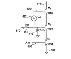
図8は、FETM3及びその上のFET(X≧3)にバイアス及びカップリングを供給するための代替案を表す。基準802は、単入力FETM1804のソースへ結合されており、M1804のゲートは、入力信号806へ結合されている。M1804のドレインは、第2のFETM2808のソースへ結合されている。バイアス電圧は、バイアス入力部810へ印加されている。バイアス入力部810は、バイアス抵抗RB812を介してM2808のゲートへ、及び比較的大きなキャパシタンスCG2814へ結合されている。M2808のドレインは、スタックの第3のFETM3816のソースへ結合されている。M3816のドレインは、存在するならば、更なるFET段へ結合されうる。しかし、最終段のFETM3816のドレインは、図8で示されるように、出力ノードVdrive818へ結合されている。
Figure 8 represents an alternative for supplying bias and coupling the FET M 3 and FET thereon (X ≧ 3).
FETM3816のゲートは、ツェナーダイオードDZ822を介して前段のFETM2808のゲートへ結合されている。DZ822は、M3のVDSのほぼ所望の最大値で導通閾値を有しても良い(ツェナーダイオードと同じように動作する回路がDZ822の代わりに用いられても良い。)。下付き文字“Y”によって示される更なるFET段が加えられても良い。このような更なる段に関して、対応する更なるツェナーダイオードは、DZ822と同じ方法で使用されうる。即ち、更なるツェナーダイオードは、そのアノードを更なるFETMYのゲートへ、且つそのカソードをM(Y−1)のゲートへ結合される。
The gate of the
[6−A.代替の積層FETスイッチ構成及び拡張]
図1〜8に関して先に説明されたFETスタックは、NチャネルFET(N−FET)を用いる。PチャネルFET(P−FET)スタックは、夫々の電圧と、スタックに結合された有極部品の極性を反転させることにより、同様に製造されうる。P−FETスタックの基準電圧は、一般的に、第1の単入力FETMP1のソースへ結合されうる。このような逆回路は、上述されたN−FETスタック回路と実質的に同じ原理に従って動作する。例えば、Vdrive818は、全てのFETがPチャネルであって、且つツェナーDZ822接続が反転される(アノードとカソードとが交換される)ならば、図8の基準802に対して負となりうる。
[6-A. Alternative stacked FET switch configurations and extensions]
The FET stack described above with respect to FIGS. 1-8 uses N-channel FETs (N-FETs). P-channel FET (P-FET) stacks can be similarly manufactured by reversing the respective voltages and polarities of the polarized components coupled to the stack. Reference voltage of P-FET stack will generally be coupled to a first source of a single-input FET M P1. Such an inverse circuit operates according to substantially the same principle as the N-FET stack circuit described above. For example,
図9は、NチャネルFETMN1902、MN2904及びMN3906を有するNチャネルFETスタック、並びにPチャネルFETMP1908、MP2910及びMP3912を有するPチャネルFETスタックの両方を用いる、例となる回路である。D級動作では、入力矩形波は、N−FETスタックへ入力部916において共通電位914に対して供給され、且つキャパシタCGP1918を介してMP1908のゲートでP−FETスタックの入力へ結合されている。バイアス電圧は、例えばP−FETスタックの基準VDD930を下回るVGS(on)の2分の1に設定されており、バイアス抵抗RBP1を介してMP1908に供給されうる。代替的に、キャパシタCGP1918及びバイアス抵抗RBP1920は削除され、入力部916及びMP1908のゲートは、夫々、代わりに、非オーバーラップクロック発生器(図示せず。)によって駆動されても良い。
FIG. 9 illustrates an example using both an N-channel FET stack with N-
N−FETのMN2904及びMN3906の制御は、(N=3の場合に)図2に関して説明された制御と実質的に同じである。MN2904のゲートは、比較的大きな値を有するキャパシタCGN2922を介して共通電位へ結合(即ち、デカップリング)されており、バイアス抵抗RBN2924を介して約(VDD/3)の電圧にバイアスされうる。MN3906のゲートは、図2に関して説明されたように計算された値を有するキャパシタCGN3926を介して共通電位とデカップリングされており、バイアス抵抗RBN3928を介して(VDD/2)の電圧にバイアスされうる。
Control of the N-
P−FETスタックは、N−FETスタックと同様に制御される。バイアス電圧の極性は反転され、この場合にはVDD930であるP−FETスタックの基準電圧を基準とする。P−FETのゲートを容量的にデカップリングするために、P−FETの基準電圧がVDD930であるという事項は、VDDが、通常は、N−FETの基準である回路共通電位914に密に結合されるので、僅かにしか相違を生じないと見込まれる。従って、キャパシタ932及び936のデカップリングは、代替的に、回路共通電位914へ接続されても良い。しかし、示されるように、MP2910のゲートは、比較的大きなキャパシタCGP2932を介してVDDへデカップリングされており、バイアス抵抗RBP2932を介して約2VDD/3へバイアスされている。MP3912のゲートは、キャパシタCGP3936を介してVDDへデカップリングされている。CGP3936の値は、X=3及びN=3の場合に図2に関して説明されたように計算されうる。MP3912のゲートは、バイアス抵抗RBP3938を介して約VDD/2へバイアスされている。
The P-FET stack is controlled similarly to the N-FET stack. The polarity of the bias voltage is reversed and in this case is referenced to the reference voltage of the P-FET stack, which is
出力電圧Vdrive940は、導通しているのがN−FETスタックかP−FETスタックかどうかに従って、共通電位とVDDとの間で駆動されうる。出力電圧Vdrive940は、図10を参照して更に詳細に以下で説明されるように、シャントフィルタ950によってシャントフィルタをかけられ、マッチング及びカップリング回路960によって処理されうる。マッチング及びカップリング回路960から、信号は、通常、伝送線路、1又はそれ以上の更なるフィルタ部、及びRFスイッチ(図示せず。)を介して、アンテナ942へ送られうる。
The
図9のシャントフィルタ950は、図4又は図6に示されたものに同様であっても良い。図9のマッチング及びカップリング回路960は、例えば、図3に示されたものと同様であっても良い。しかし、図10は、図9の回路のブロック950及び960の両方に用いられ得るフィルタリングを表わす。キャパシタCS952は、シャントフィルタ950として働きうる。図10の残りの構成要素は、図9のマッチング及びカップリング回路960として機能しうる。インダクタLC954は、物理的なカップリング接続を有しうる。カップリングキャパシタCC962は、直流を遮断する働きをする。LA964、CA966、LB968及びCB970は、出力インピーダンスZOUTに整合するために構成されうる。出力インピーダンスZOUTは、通常、50Ωである。
The
[7.モノリシック構造で集積された中電力デュアルバンドRF送信機]
RF送受信機は、例えば図12に表わされたデュアルバンドRF送受信機のように、通常、図12の項目1226又は1256のような受信信号増幅器を有する。このような受信信号増幅器は、通常、低雑音増幅器(LNA)であり、アンテナから受信された信号を調整するために用いられる。RFフロントエンドは、LNAを必ずしも含まないRF送受信機回路と考えられることがある。
[7. Medium power dual-band RF transmitter integrated in monolithic structure]
The RF transceiver typically has a received signal amplifier, such as
ほとんどのRF送受信機で、ディスクリート集積回路(IC)は、完全なRFフロントエンド部を作るためにモジュールと一体化されるべきである。通常は、少なくともアンテナスイッチは、PAとは異なる別々のIC上に作られ、しばしば、多数の更なるディスクリートICが、RFフロントエンドモジュールを作るために外部配線を介して接続されなければならない。夫々のこのようなディスクリートICは、それに含まれるディスクリートICが異なるロットから提供される場合、又は同じタスクを実行する他のICとは違うふうに設計され、作られた場合でさえ、適切にそのモジュール機能を確実にする特定の性能要件によって決定されるべきである。このような性能要件は、種々様々なものを組み合わせて作った柔軟性及び信頼性を達成するためにこのように作成されており、これらのデバイスと一体化されるディスクリートICのための費用を相当に必要とする。 With most RF transceivers, a discrete integrated circuit (IC) should be integrated with the module to create a complete RF front end. Usually, at least the antenna switch is made on a separate IC different from the PA, and often a number of additional discrete ICs must be connected via external wiring to make an RF front-end module. Each such discrete IC is adequately suited even if the discrete ICs it contains are provided from different lots or even designed and made differently from other ICs that perform the same task. Should be determined by specific performance requirements to ensure module functionality. Such performance requirements have been created in this way to achieve the flexibility and reliability made by combining a wide variety of things, which represents a cost for discrete ICs integrated with these devices. Need to.
多重IC送受信機モジュールにおけるPAは、通常、要求に応じて十分な電力の信号を生成する。アンテナスイッチユニットは、期待されるアンテナインピーダンス(例えば、50Ω)に整合された送信信号、又は受信信号入力のいずれか一方へアンテナ(より正確には、アンテナ接続部)を結合する。しかし、アンテナ接続部又はアンテナへのダメージは、アンテナ接続線路からアンテナ接続点へ反射されたインピーダンスを、その期待値から大幅に変化させうる。このような場合に、大きな電圧定在波(VSW)は、その反射インピーダンスと、送信信号が整合される期待値との間で結果として得られる不整合によって引き起こされうる。通常動作中に期待されるよりもずっと大きい電圧偏位が、このような不整合により誘引されたVSWの結果として発生しうる。アンテナスイッチの耐圧要求は、通常、このような不整合状態の下でのダメージを回避するよう、通常のピーク動作電圧よりもずっと高く設定される。 A PA in a multi-IC transceiver module usually generates a signal with sufficient power as required. The antenna switch unit couples the antenna (more precisely, the antenna connection) to either the transmission signal or the reception signal input matched to the expected antenna impedance (for example, 50Ω). However, the damage to the antenna connection portion or the antenna can significantly change the impedance reflected from the antenna connection line to the antenna connection point from the expected value. In such cases, a large voltage standing wave (VSW) can be caused by the resulting mismatch between its reflected impedance and the expected value to which the transmitted signal is matched. A much larger voltage excursion than would be expected during normal operation can occur as a result of VSW induced by such a mismatch. The breakdown voltage requirement of the antenna switch is usually set much higher than the normal peak operating voltage so as to avoid damage under such mismatch conditions.
例えばアンテナスイッチのような電力切替え回路におけるスイッチングデバイス(例えばFET)によって占有されるIC面積は、それらが耐えることができる電圧の2乗で増大しうる。従って、所要の耐圧を半分にすると、スイッチデバイス面積は1/4まで低減される。更に、これらのデバイスは、アンテナ切替え回路によって使用されるIC面積の大半を占めるから、IC面積(ひいては製造費用)の非常に大幅な節約が、それらの所要の耐圧を下げることにより実現されうる。このような低減は、ディスクリートICが送受信機全体を作るために結合されるべき場合には現実的ではない。しかし、PAから、アンテナスイッチを介して、更にアンテナ接続部まで全てのデバイスを含む単一ICは、高い不整合により誘引されたVSWに対して保護するよう、信頼性のある内部カップリング及び密なデバイス整合を活用しうる。集積に関するこれらの利点に起因して、デバイス面積の大幅な節約が、同等に機能する送受信機を作るようディスクリートICを一体化することに比べて、達成可能である。 The IC area occupied by switching devices (eg FETs) in power switching circuits such as antenna switches can increase with the square of the voltage they can withstand. Therefore, when the required breakdown voltage is halved, the switch device area is reduced to ¼. Furthermore, since these devices occupy most of the IC area used by the antenna switching circuit, a very significant savings in IC area (and hence manufacturing costs) can be realized by reducing their required breakdown voltage. Such a reduction is not practical when discrete ICs are to be combined to make the entire transceiver. However, a single IC that includes all devices from the PA, through the antenna switch, and even to the antenna connection, has reliable internal coupling and tightness to protect against VSW induced by high mismatch. Device matching can be used. Due to these advantages with respect to integration, significant device area savings can be achieved compared to integrating discrete ICs to create equivalently functioning transceivers.
図12は、このような集積保護の利益を享受するよう構成されたデュアルバンド送受信機の主要なRF部の簡単なブロック図である。第1の動作周波数FO1での低レベル信号は、同じICチップ上にある(しかし、必ずしもその必要はない。)供給源から入力ノード1202へ結合される。信号は、増幅器1204により示されるような、如何なる適切な増幅器によっても増幅される。増幅器1204により生成された信号は、パルス調整回路1500が矩形性を改善するよう、更に、望ましくは、最終的に電力増幅器(PA)1206に結合される波形のデューティーサイクルを調整するよう設けられる場合には、好ましい矩形形状から著しく外れても良い。
FIG. 12 is a simplified block diagram of the main RF portion of a dual-band transceiver configured to enjoy such integrated protection benefits. The low level signal at the first operating frequency F O1 is coupled to the
パルス調整回路1500の出力は、PA1206への入力である。PA1206は、電源114から、直列レギュレータ1400及びRFチョーク(RFC)LS108を有する電源調整素子を介して電力を引き込んで、PA出力信号を発生させる。PA出力信号は、入力信号、PA回路素子、及び電源調整素子から生ずる特性インピーダンスを有しており、一般的に、アンテナノード1214で期待されるインピーダンスとは異なる。カップリング、マッチング及びフィルタリング回路は、例えばブロック1210によって表されるように、必要とされても良い。このような回路は、直流を遮断しながら、PA出力信号をアンテナスイッチへ結合し、更に、所望のアンテナノードインピーダンス(例えば50Ω)へとPA出力インピーダンスを変換しうる。それは、また、PA出力信号をアンテナスイッチ1700のA入力部へ結合する前に、PA出力信号から、例えばFO1の高調波などの不要な信号成分をフィルタ処理しうる。別々の接地が設計優先の問題として保持される場合には、カップリング、マッチング及びフィルタリングブロック1210の出力は、接地基準112を基準としても良い。接地基準112は、回路内の他の場所で使用される回路共通基準104とは区別されても良い。アンテナスイッチ1700は、ICチップから分離されうるアンテナへ、例えば伝送線路によって、結合されるアンテナノード1214へ信号を選択的に結合する。
The output of the
PA(及び全ての介在する回路)と同じICチップ上でのアンテナスイッチのアンテナ接続の有効性は、アンテナスイッチ回路によって、PAによって、又はカップリング、マッチング若しくはフィルタリング素子によって耐えられるべき最大の電気的ストレスを確実に制限する機会を提供する。出力センサ1600は、電気的ストレスを検知して、電気的ストレスが過度である場合にPAにその出力を下げさせる信号を供給するよう、アンテナノード1214へ結合されても良い。この目的のために、出力センサ1600の出力部1220は、PA制御ブロック1300の入力部Bへ結合されている。PA制御ブロック1300へのA入力部1224は、PA出力信号の包絡線振幅を調整するよう振幅制御信号を受信しても良い。この入力部は、また、PAからの出力を制限する、あるいは終端するために使用されても良い。A及びBの両入力部は、PA制御ブロック1300から直列レギュレータブロック1400へ結合された出力Dに影響を及ぼしうる。PA制御ブロック1300へのC入力部1222は、ブロック1300からのE出力を制御する情報又は信号を供給しても良い。E出力部は、PA1206へ入力される矩形波のデューティーサイクルを制御するようパルス調整回路1500へ結合されても良い。デューティーサイクル制御は、例えば、PA出力信号の電力レベルを下げるよう他の手段を設けても良い。入力部1202からの信号経路は、fO1を含む動作周波数の第1の帯域に関して調整されても良い。
The effectiveness of the antenna connection of the antenna switch on the same IC chip as the PA (and all intervening circuits) is the maximum electrical to be withstood by the antenna switch circuit, by the PA, or by coupling, matching or filtering elements. Provide an opportunity to reliably limit stress. The
アンテナスイッチ1700は、入力部Aでの第1の帯域送信信号からアンテナノード1214を選択的に切り離し、第1の受信帯域に関してアンテナから受信前置増幅器1226へと受信された信号を伝送するように代わりに出力部Bへアンテナノード1214を結合する。望ましくは、受信前置増幅器1226(及び1256)は、低雑音増幅器(LNA)である。LNAは、ここで説明されるような集積されたフロントエンドに必ずしも含まれないが、それらは、通常、完全な送受信機回路に含まれる。受信前置増幅器1226からの出力は、存在するならば、同じICチップ上又はその外部の更なる第1の受信帯域回路へ伝送されても良い。アンテナスイッチ1700は、同様に、アンテナノード1214を第2の受信帯域前置増幅器1256へ選択的に結合して、アンテナから第2の受信帯域出力ノード1258への信号を増幅する。その出力は、ICチップ上又はその外部の更なる第2の受信帯域回路へ伝送されても良い。
The
同様に、第1の送信帯域回路に関して先に説明されたように、第2の動作周波数帯域内の第2の動作周波数fO2にある送信信号は、入力部1232へ供給されて、増幅器1234により増幅されても良い。増幅器1234から出力される信号のデューティーサイクル及び波形は、PA制御ブロック1301の制御下にあるパルス調整回路1501によって調整されて、第2の帯域PA1207への入力として送られる。第2の帯域PA1207は、RFチョーク109を介して、PA制御ブロック1301の制御下にある直列レギュレータ1401によって制限されるように、VDD114から供給される電力を用いて第2の帯域PA出力信号を発生させうる。第2の帯域PA出力は、特性インピーダンスを有しており、ブロック1211を介してアンテナスイッチ1700のD入力部へ結合される。ブロック1211は、信号を結合し、PA出力とアンテナノードインピーダンスとを整合させ、出力信号をフィルタ処理する。アンテナスイッチ1700は、アンテナノード1214へD入力部を結合するよう制御される。信号は、アンテナノード1214からアンテナ1216へ伝送される。出力センサ1600の出力部1220は、また、第2の帯域PA制御ブロック1301へのB入力部へ結合されても良い。これによって、過度の出力電圧は、第2の帯域PA出力信号を安全なレベルまで低減させられる。第2の帯域PA制御ブロック1301は、また、C入力部1252でのデューティーサイクル制御信号はもちろん、A入力部1254での包絡線制御信号を受け取っても良い。
Similarly, as described above with respect to the first transmission band circuit, the transmission signal at the second operating frequency f O2 in the second operating frequency band is supplied to the
示されないが、望ましくは、制御回路は、関連するPAが作動する場合にのみ有効とされる。例えば1300又は1301等のPA制御ブロックの例となる回路は図13に示される。例えば1400又は1401等の直列レギュレータの例となる回路は図14に示される。例えば1500又は1501等のパルス調整回路の例となる回路は図15に示される。PA1206又は1207は、図1のブロック400などのシャントフィルタ、又は図11の適切な素子とともに、図1のドライバ素子ブロック200に関して説明されたように作られても良い。カップリング、マッチング及びフィルタリング回路1210及び1211は、図3又は図10に関して先で説明されたように、あるいは同様のカップリング、マッチング及びフィルタリング効果を得られる如何なる他の方法で作られても良い。留意すべきは、図11に示されるような回路が用いられるべき場合には、カップリングキャパシタ302はシャントフィルタの前に配置され、マッチング及びフィルタリングはブロック990と同じく、その後に設けられることである。
Although not shown, preferably the control circuit is enabled only when the associated PA is activated. An example circuit of a PA control block, such as 1300 or 1301, is shown in FIG. An example circuit of a series regulator such as 1400 or 1401 is shown in FIG. An example circuit of a pulse adjustment circuit such as 1500 or 1501 is shown in FIG.
図13は、PA制御ブロック1300の回路例を表す。イネーブル入力部A1302は、入力部1302がほぼ接地電位である場合に、出力部D1306が電流を引き込まないように、FET1304へ直接的に結合されても良い。出力部D1306への導通は、出力部1306が電流を導かない場合に、電流がPAへ供給されずに、図14に関して以下で説明されるように出力電力を零まで低下させるように、図14に示されるような直列レギュレータを介してPA出力電力を制御しうる。FET1308は、抵抗1310及び1312によってバイアスされる。抵抗1310及び1312は等しい値を有し、例えば30〜50Ωといった公称値は工学上の便宜のために選択される。この構成は、低電圧FETを保護して、FET1304、1308及び1314の全てのVGD、VGS及びVDSが著しくVDD/2を超えないことを確実にする。
FIG. 13 shows a circuit example of the
電力検知入力部B1316は、抵抗1318へ結合されうる。抵抗1318は、約30〜50Ωであって、演算増幅器1322の利得1を確立するよう抵抗1320に十分に等しい。電力設定入力部C1324は、一実施例において、0Vから2*Vth(FETの閾値電圧)までに設定される。なお、Vthは、0.4〜0.7Vであって、通常は約0.5Vであり、回路内で一貫している。演算増幅器1322の非反転入力は、ダイオード接続FET1328及び1330とともに抵抗1326(例えば30〜50Ω)を用いて、この電圧範囲を超えることを防止され、このようにして、選択されうる最大電力を制限する。当業者は、選択可能な出力電力を不変な回路設計最大値とするように、回路値及び回路設計を変更することができる。具体的には、ダイオード接続FET1328及び1330の一方又は両方は、例えば電力設定及び出力電圧制限の精度を向上させるよう、バンドギャップ基準を含む回路により置換されても良い。多数の他の技術、同様の効果を達成するために用いられても良い。電力検知入力B1316が電力設定入力電圧により定められた値を超える場合に、FET1314は、導通を中断して、出力部D1306への導通を妨げる。
The power sense input B1316 can be coupled to a
PA制御ブロック1300は、また、図12のパルス調整回路1500によって実行されるデューティーサイクル調整を制御するよう出力部E1512を設ける。基準電圧は、製造工程パラメータなどの要素に従って調整可能であって、入力部1332に供給される。この電圧は、等分抵抗1336及び1338の制御下で演算増幅器1334によって2倍にされる。当然、他の実施例では、図13に示されるような回路の利得は、異なることが考えられ、例えば、1336及び1338などの、このような利得を設定する抵抗は、然るべく値が異なる。幾らかデューティーサイクルを低減することにより、PA出力電力は対応して低下し、それを零まで低減することにより、PA出力は全体的に抑制されうる。抵抗1336及び抵抗1338により従来の方法でその利得を制御されうる増幅器1334の入力部1338へ供給される基準電圧は、ブロック1500の出力デューティーサイクルを制御するよう、出力部Eで電圧を発生させる働きをする。
The
図14は、PAへ供給される実効電圧を制限して、ひいてはPA出力振幅を制限するための例となる直列レギュレータ回路1400を表す。入力部1306へ供給される電圧は、VDDと比較して、PチャネルFET1402を制御し、更に、いずれか2つのノード間の過電圧からFET1402を保護するよう、抵抗1406及び1404を介して分割されている。PチャネルFET1408は、FET1402と1408との間でほぼ同様に、VDDと出力部1414との間で発生した最大電圧を分割するように、抵抗1410及び1412によってバイアスをかけられている。出力部1414は、RFチョークを介してPAへ電力を供給する。FET1402及び1408は、例えば、−0.4Vから−0.7Vの間のVGS閾値電圧を有する。抵抗1404、1406、1410及び1412は、全て実質的に等しく、例えば30〜50Ωであるよう工学上の便宜のために選択された大きさを有しても良い。これらの例となる値及び相対的値は、工学上の便宜のために変更されても良い。
FIG. 14 illustrates an example
図15は、例となる信号調整回路1500の回路図である。入力信号は、入力ノード1502で供給されて、ダイオード接続FET1504を介してインバータ1506の入力部へ結合されうる。FET1504のVDS閾値を加えた入力信号電圧がインバータ1506の閾値よりも低い場合には、インバータ1508の出力は低電位(low)となる。しかし、入力信号の電圧がこの値を上回る場合には、FET1504は導通を中断する。その後、入力部1502の電圧が極めて高い(例えばVDD)場合でさえ、入力部からの電流は、入力電圧1512の制御下でPチャネルFET1510によって制限される。FET1510を流れるこのような電流は、インバータ1506への入力がそのスイッチング閾値を上回るまで、(約0.25〜0.5pFの金属−絶縁−金属、即ちMIMキャパシタでありうる)キャパシタ1514を充電すべきである。その時点で、インバータ1506及び1508がキャパシタ1514を介する正のフィードバックにより急速に状態を変化させて、出力ノード1516で矩形端を生じさせる。立ち上がり及び立ち下がり時間は、主にインバータ1506及び1508による遅延により制限される。入力部1502での信号が、おおよそ、約50%デューティーサイクルの矩形波である場合には、制御入力部1512での電圧は、出力デューティーサイクルが50%から、零に達するほど任意により低い値へと低減される。入力信号は、出力デューティーサイクルの幅がより広いことが望まれる場合に、50%を超えるデューティーサイクルを有するよう構成されても良い。
FIG. 15 is a circuit diagram of an exemplary
図16は、検知ノード1602でピーク電圧を検知するための例となる回路1600の回路図である。検知ノード1602は、例えば、図12のアンテナノード1214へ直接的に接続されても良い。入力分割器は、比較的高い電圧を検知するために、示されるように使用されうる。例えば1kΩといった比較的低い抵抗値を有する4つのほぼ等しい抵抗1604、1606、1608及び1610が使用されても良い。ダイオード接続FET1612は、この電圧が高い場合に導通して、約24kΩの抵抗1614を介して約1pFのキャパシタ1616へ電流を供給する。抵抗1614及びキャパシタ1616によって決定される時定数が、(PA出力信号の所定のレベルに関して)出力電圧を上昇させうる如何なる事象の存続期間よりもずっと小さい限りは、多数の他の値が用いられても良い。例えば、アンテナインピーダンスを設計値から大幅に変化させて、高電圧定在波を発生させるアンテナの機械的事象は、発生するのに少なくとも数ミリ秒を要する。例となる回路1600の約24nsの時定数は、このような事象存続期間を十分に下回る。しかし、それらの要素に起因するコーナー周波数は、回路発振を回避するために、一般的に、第1及び第2の帯域動作周波数fO1及びfO2の両方を十分に下回るべきである。事象存続期間が1/fOに近づく場合に、他の共通の回路設計配慮は、過電圧を防ぐほど十分に応答が速いことを確実にしながら発振を回避するよう、更に複雑な回路を必要としうる。
FIG. 16 is a circuit diagram of an
図17は、アンテナスイッチの例となる回路1700の簡単化された図である。このようなRFスイッチの設計及び製造に関する更なる詳細は、2004年10月12日に出願され、「無線周波数信号を切り替えるスイッチ回路及び方法(Switch Circuit and Method of Switching Radio Frequency Signals)」と題された米国特許番号6,804,502号で知られる。制御信号を供給する回路は、図示されない。更に、制御電圧は、望ましくは、VDDに近い高電位(high)又は−VDDに近い低電位(low)のいずれか一方であるべきである。−VDD制御電圧を発生させるよう、負電圧発生器が有用であり、望ましくは、例えば、2003年9月8日に出願され、「低雑音電荷ポンプの方法及び装置(Low Noise Charge Pump Method and Apparatus)」と題された米国特許公開番号10/658,154号に記載されるような低雑音回路が用いられる。このような低雑音電荷ポンプは、アンテナからの意図されない放射を回避するために重要である。
FIG. 17 is a simplified diagram of an
ポートノード1780は、スイッチ1700の共通接続部である。図12において、スイッチ1700の共通接続部は、アンテナノード1214へ結合されている。共通接続部は、一般的に、1度に1つのRFポート(ポートA1710、ポートB1730、ポートC1750、又はポートD1770)のみへ結合される。夫々のRFポートは、対応する“+”制御ノードと、対応する“−”制御ノードとを有する。ポートA、B、C及びDに関して、“+”制御ノードは、夫々、ノード1708、1728、1748及び1768であり、一方、“−”制御ノードは、夫々、ノード1718、1738、1758及び1778である。
The
共通接続部へRFポートを結合するよう、“高”電圧(〜VDD)はポートの対応する“+”制御ノードへ印加され、一方、“低”電圧(〜−VDD)はポートの対応する“−”制御ノードへ印加される。その間に、“低”電圧は、他のRFポートに対応する夫々の“+”制御ノードへ印加され、“高”電圧は、他のRFポートに対応する夫々の“−”制御ノードへ印加される。それによって、選択されたRFポートは、共通接続部へ結合され、一方、全ての他のRFポートは、接地へ結合されうる。従って、共通接続部1780へRFポートA1710を結合するよう、“高”電圧は制御ノード1708、1738、1758及び1778へ印加され、一方、“低”電圧は全ての他の制御ノード(1718、1728、1748及び1768)へ印加される。
A “high” voltage (˜VDD) is applied to the corresponding “+” control node of the port to couple the RF port to the common connection, while a “low” voltage (˜−VDD) is applied to the corresponding “ -"Applied to the control node. Meanwhile, a “low” voltage is applied to each “+” control node corresponding to the other RF port, and a “high” voltage is applied to each “−” control node corresponding to the other RF port. The Thereby, the selected RF port can be coupled to the common connection, while all other RF ports can be coupled to ground. Thus, a “high” voltage is applied to control
全ての抵抗は、通常、同じ値を有する。ある実施例では、その値はおよそ30〜50Ωである。抵抗は、FET(例えばM1A1701)の寄生ゲート容量の時定数が、その対応するゲート抵抗(例えば1704)の値とともに、fOが制御されるRF信号の最小周波数である場合に、1/fOよりもずっと大きくなるように選択される。表される構成は、FETスタック(例えば、FETM1A1701、M1B1702及びM1C1703から成るスタック、FETM2A1704、M2B1705及びM2C1706から成るスタックなど)の両端に現れる電圧を均一に分割する働きをして、圧縮効果を低減する。スイッチング機能を提供するFETスタック(例えば、FET1701、1702及び1703)は、説明のために示された3よりも多い又は少ないデバイスを有しても良い。少なくとも9個のデバイスから成るスタックが、うまく作られている。電圧ストレス分布一様性に起因して、幅広い信号電圧及び製造工程パラメータが適合されうる。
All resistors usually have the same value. In one embodiment, the value is approximately 30-50Ω. Resistance, if the time constant of the parasitic gate capacitance of the FET (eg M1 A 1701), along with the value of the gate resistance (e.g. 1704) to the corresponding a minimum frequency of the RF signal f O is controlled, 1 / It is chosen to be much larger than
[集積回路の製造及び設計]
集積回路製造の詳細は、上記で示されていない。約2.4GHzで1Wより過度に出力電力を有するものも含め、幾つかの好ましい実施例で、集積回路は、1997年9月2日に公報が発行され、「サファイヤチップ上の単一極薄シリコンにおける高周波無線通信システム(High−Frequency Wireless Communication System on a Single Ultrathin Silicon On Sapphire Chip)」と題された米国特許番号5,663,570号に記載されるようなサファイヤ処理における極薄シリコンに従って作られても良い。他のセミコンダクタ・オン・インシュレータ(SIO)技術は、少なくとも幾つかの周波数帯域及び電力レベルに関して、上述されたデュアルバンド送受信機集積回路を作るために使用されても良い。
[Manufacture and design of integrated circuits]
Details of integrated circuit fabrication are not shown above. In some preferred embodiments, including those having an output power of more than 1 W at about 2.4 GHz, the integrated circuit was published on September 2, 1997, saying "Single ultrathin on sapphire chip. Ultra-thin silicon in sapphire processing as described in US Pat. No. 5,663,570 entitled “High-Frequency Wireless Communication System on a Single Ultrathin Silicon On Sapphire Chip”. May be. Other semiconductor-on-insulator (SIO) technologies may be used to make the dual-band transceiver integrated circuit described above for at least some frequency bands and power levels.
上記の好ましい集積回路製造技術は、むしろ低い最大値VDSを有するFETを容易に作る。従って、様々な技術は、一貫性のある工程を維持しながらより高い電圧の制御を実現するよう、FETをスタックすることについて説明される。他の製造技術又はより低い電圧及びインピーダンスを用いると、カスコード又は多重積層FETに対する必要性は回避可能となりうる。 Additional preferred integrated circuit fabrication techniques make it easier to FET having a rather low maximum value V DS. Accordingly, various techniques are described for stacking FETs to achieve higher voltage control while maintaining a consistent process. Using other manufacturing techniques or lower voltages and impedances, the need for cascode or multi-layered FETs can be avoided.
[結び]
上記は、集積回路における一対のノード間の導通を制御するよう積層トランジスタを用いる方法及び装置の実施例及び新規な特徴について説明する。当業者には明らかであるように、表される方法及び装置の形状及び詳細に対する様々な削除、置換及び変更は、本発明の適用範囲から逸脱することなく行われる。多数の代わりの実施例が考えられるが、全ての実施例を明示的に列挙することは実際的ではない。このようにして、先に挙げられ、且つ/あるいは示された装置又は方法の代替案の夫々の実際的な組み合わせは、主たる装置又は方法の明確な代替実施例を構成する。このような装置又は方法の代替案の均等に係る夫々の組み合わせは、また、主たる装置又は方法の明確な代替実施例を構成する。従って、本発明の適用範囲は、添付の特許請求の範囲によってのみ決定されるべきであり、このような制限が添付の特許請求の範囲で挙げられる又は意図的に関係する限りにおいて、先に示された特徴によって制限されるべきではない。
[Conclusion]
The above describes embodiments and novel features of methods and apparatus that use stacked transistors to control conduction between a pair of nodes in an integrated circuit. It will be apparent to those skilled in the art that various deletions, substitutions, and modifications to the form and details of the methods and apparatus represented can be made without departing from the scope of the invention. Many alternative embodiments are possible, but it is not practical to explicitly list all embodiments. In this way, each practical combination of alternatives of the apparatus or method previously listed and / or shown constitutes a clear alternative embodiment of the main apparatus or method. Each such equivalent combination of apparatus or method alternatives also constitutes a clear alternative embodiment of the primary apparatus or method. Accordingly, the scope of the present invention should be determined only by the appended claims, and as long as such limitations are recited or intentionally related to the appended claims, Should not be limited by the features made.
明らかなように、集積に係る同様の利点が、他の機能ブロックを有する回路のものとなりうる。例えば、混合器は、このような装置に組み込まれても良く、送信信号処理の更なる部分の集積を可能となる。位相ロックループは、RFフロントエンド又は送受信機と同じモノリシックIC上で送信信号を発生させるよう能力を更に高めうる。更なる形式のフィルタは、受信及び送信の処理のいずれか一方又は両方に対して有用となりうる。 As will be apparent, similar benefits associated with integration can be for circuits having other functional blocks. For example, the mixer may be incorporated into such a device, allowing further parts of the transmitted signal processing to be integrated. The phase locked loop may further enhance the ability to generate a transmit signal on the same monolithic IC as the RF front end or transceiver. Additional types of filters can be useful for either or both of the receive and transmit processes.
様々な請求要素の均等の意味及び範囲内で生ずる全ての変形は、対応する請求項の適用範囲内に包含される。夫々の請求項は、このようなシステム又は方法が従来技術の実施例でない場合に、このような請求項の文言としか非現実的には異ならない如何なるシステム又は方法をも包含する。この目的のために、夫々の請求項で記載される夫々の要素は、可能な限り幅広く解釈されるべきであり、更に、従来技術を包含せずに可能な程度にこのような要素と等価な如何なるものをも包含すると理解されるべきである。 All changes that come within the meaning and range of equivalency of the various claim elements are included within the scope of the corresponding claims. Each claim encompasses any system or method that, if such a system or method is not an example of the prior art, differs only in unrealistic terms from such claims. For this purpose, each element recited in each claim should be construed as broadly as possible, and further equivalent to such element to the extent possible without including the prior art. It should be understood to encompass anything.
本願は、2004年6月23日に出願され、「積層トランジスタに係る方法及び装置(Stacked Transistor Method and Apparatus)」と題された、同時継続中であって、通例譲渡された米国特許出願番号10/875,405に対する優先権の主張を伴うものであり、以下の公知の米国特許文献、即ち、1997年9月2日に公報が発行され、「サファイヤチップ上の単一極薄シリコンにおける高周波無線通信システム(High−Frequency Wireless Communication System on a Single Ultrathin Silicon On Sapphire Chip)」と題された米国特許番号5,663,570号と、2004年10月12日に出願され、「無線周波数信号を切り替えるスイッチ回路及び方法(Switch Circuit and Method of Switching Radio Frequency Signals)」と題された米国特許番号6,804,502号と、2003年9月8日に出願され、「低雑音電荷ポンプの方法及び装置(Low Noise Charge Pump Method and Apparatus)」と題された同時継続中の米国特許公開番号10/658,154号とに関連しており、これら4つの米国特許文献の夫々の内容は、参照することによりその全体を本願に援用される。 This application was filed on June 23, 2004 and is a co-pending, commonly assigned U.S. Patent Application No. 10 entitled “Method and Apparatus for Stacked Transistors (Stacked Transistor Method and Apparatus)”. With the claim of priority to / 875,405, the following known U.S. patent document, published on September 2, 1997, "High-frequency radio in single ultra-thin silicon on sapphire chips" US Pat. No. 5,663,570 entitled “High-Frequency Wireless Communication System on a Single Ultrathin Silicon On Sapphire Chip”, issued October 12, 2004 No. 6,804,502, filed Sep. 8, 2003, entitled "Switch Circuit and Method of Switching Radio Frequency Signals" In connection with the co-pending U.S. Patent Publication No. 10 / 658,154 entitled "Low Noise Charge Pump Method and Apparatus". The contents of each are incorporated herein by reference in their entirety.
Claims (16)
a)実質的に送信に適した周波数成分及び位相を有する送信信号を受信し、前記送信信号を増幅して、増幅送信信号を発生させるよう構成されるRF信号増幅器と、
b)前記増幅送信信号から取り出される入力信号へ結合される入力ノードを有し、前記入力信号を増幅して、電力増幅器出力特性インピーダンスを有する電力増幅送信信号を発生させるよう構成され、更に、前記電力増幅送信信号の振幅を制御可能なように抑制するよう構成されるレギュレータ回路を有するRF電力増幅器(PA)と、
c)直流成分を遮断し、前記電力増幅送信信号の特性インピーダンスを変更し、不要な周波数を受け入れないことによって前記電力増幅送信信号を調整して、アンテナ整合送信信号を発生させるよう構成されるマッチング、カップリング及びフィルタリング回路と、
d)前記アンテナ整合送信信号をアンテナ接続ノードへ制御可能なように結合するよう、又は前記アンテナ接続ノードを前記アンテナ整合送信信号から切り離し、代わりに前記アンテナ接続ノードを受信信号増幅経路へ結合するよう構成されるアンテナスイッチと、
e)前記アンテナスイッチを介して結合される前記送信信号の少なくとも振幅を反映する送信電力信号を発生させるよう構成される送信信号検知回路と、
f)前記アンテナスイッチにより結合される前記送信信号の振幅が所定の制限を超えることを実質的に防ぐように、前記レギュレータ回路に前記送信電力信号に応答して前記電力増幅送信信号を抑制させるよう構成される制御回路とを有する集積回路。An RF front end integrated circuit on a monolithic integrated circuit, comprising:
a) an RF signal amplifier configured to receive a transmission signal having a frequency component and phase substantially suitable for transmission, amplify the transmission signal, and generate an amplified transmission signal;
b) having an input node coupled to the input signal extracted from the amplified transmission signal, amplifies the input signal, is configured to generate a power amplified transmission signal having a power amplifier output characteristic impedance, further wherein An RF power amplifier (PA) having a regulator circuit configured to controllably control the amplitude of the power amplified transmission signal;
c) Matching configured to block the DC component, change the characteristic impedance of the power amplified transmission signal, adjust the power amplified transmission signal by not accepting unwanted frequencies, and generate an antenna matched transmission signal Coupling and filtering circuits;
d) to controllably couple the antenna matching transmit signal to an antenna connection node, or to disconnect the antenna connection node from the antenna matching transmit signal and instead couple the antenna connection node to a received signal amplification path. An antenna switch configured; and
e) a transmit signal detection circuit configured to generate a transmit power signal reflecting at least the amplitude of the transmit signal coupled via the antenna switch;
f) causing the regulator circuit to suppress the power amplified transmission signal in response to the transmission power signal so as to substantially prevent an amplitude of the transmission signal coupled by the antenna switch from exceeding a predetermined limit. An integrated circuit having a control circuit configured.
前記シャントフィルタは、著しく抵抗性を有するインピーダンスを介して動作周波数fOの整数高調波である1又はそれ以上の高調波での前記電力増幅送信信号の信号成分を導き、一方、前記動作周波数fOでの信号成分を実質的に受け入れないよう構成される、請求項4記載の集積回路。The RF power amplifier has only one switching device having one or more FETs that conduct at substantially the same time, and further includes a shunt filter disposed between the output drive node and the circuit common part. And
The shunt filter guides the signal component of the power amplified transmission signal at one or more harmonics, which are integer harmonics of the operating frequency f O , through a significantly resistive impedance, while the operating frequency f 5. The integrated circuit of claim 4, wherein the integrated circuit is configured to substantially not accept a signal component at O.
請求項1の前記項目(c)に従うが、第2のアンテナ整合送信信号を生成するよう構成される第2のマッチング、カップリング及びフィルタリング回路とを更に有し、
前記アンテナスイッチは、更に、前記第2のアンテナ整合送信信号へだけ、又は第2の受信信号増幅経路へだけ前記アンテナ接続ノードを制御可能なように結合するよう構成される、請求項1記載の集積回路。In accordance with item (b) of claim 1, a second RF power amplifier having a regulator circuit that accepts an input signal at a second operating frequency f and is controlled by a signal from the transmission signal sensing circuit;
According to item (c) of claim 1, further comprising a second matching, coupling and filtering circuit configured to generate a second antenna matched transmit signal,
The antenna switch of claim 1, wherein the antenna switch is further configured to controllably couple the antenna connection node only to the second antenna matched transmit signal or only to a second receive signal amplification path. Integrated circuit.
a)動作周波数fOでRF入力信号を受信するよう構成される入力ノードと、
b)実質的に線形動作を回避するために、前記RF入力信号の制御下で、オンインピーダンスを介して回路共通部へ前記出力駆動ノードを結合するよう、又は前記回路共通部から前記出力駆動ノードを実質的に切り離すよう構成されるスイッチング回路と、
c)電源VDDと前記出力駆動ノードとの間に結合され、前記スイッチング回路動作の制御下で前記動作周波数fOにおいて略正弦波である波形を有する電流を伝送するよう構成されるRFチョーク(RFC)と、
d)前記出力駆動ノードと前記回路共通部との間に配置され、前記動作周波数fOの整数高調波である周波数を有する出力駆動信号の成分に関して、前記RF電力増幅器の特性出力インピーダンスZOの抵抗成分にほぼ等しい抵抗成分を有する終端インピーダンスZTを介して電流を導くよう構成されるシャントフィルタとを有するRF電力増幅器。An RF power amplifier (PA) configured to generate an output signal at an output drive node,
a) an input node configured to receive an RF input signal at an operating frequency f O ;
b) coupling the output drive node to the circuit common through an on-impedance under control of the RF input signal, or from the circuit common to the output drive node, to substantially avoid linear operation A switching circuit configured to substantially disconnect
c) an RF choke (RFC) coupled between a power supply VDD and the output drive node and configured to transmit a current having a waveform that is substantially sinusoidal at the operating frequency f O under control of the switching circuit operation. )When,
d) disposed between said output drive node and said circuit common, the operation with respect to the frequency f O component of the output drive signal having a frequency which is an integer harmonic of the RF power amplifier characteristic output impedance Z O of RF power amplifier having a shunt filter configured to conduct current through the terminating impedance Z T which have approximately equal resistance component to a resistance component.
前記得られる信号は、前記入力調整回路により制御されるデューティーサイクルを有する略矩形である波形を有する、請求項11記載のRF電力増幅器。An input conditioning circuit coupled to the input node and configured to provide a signal derived from the RF input signal to control the switching circuit;
The RF power amplifier of claim 11, wherein the resulting signal has a substantially rectangular waveform with a duty cycle controlled by the input conditioning circuit.
a)前記チップから離れたアンテナへ前記RFフロントエンドを結合するための1つの単独アンテナ接続ノードを設け、
i)送信信号振幅を反映する信号を発生させるよう構成される送信信号検知回路と、
ii)前記チップ上に配置されるアンテナスイッチの共通接続と
へ前記アンテナ接続ノードを結合するステップと、
b)受信送信信号を増幅するよう構成される送信信号増幅器へ入力信号ノードを結合するステップと、
c)略線形な動作でなければ、出力駆動ノードを回路共通へ切り替えるように、又は略線形な動作であれば、前記増幅された受信送信信号から得られる制御下で、前記出力駆動ノードが動作周波数fOで特性インピーダンスZdriveを有するように、スイッチングモードで動作するよう構成されるスイッチング回路を有する電力増幅器(PA)をレイアウトするステップと、
d)RFチョーク(RFC)の第1の接続へ前記電力増幅器の前記出力駆動ノードを結合し、前記RFCの第2の接続をレギュレータ回路を介して電源へ結合するステップと、
e)前記アンテナ接続ノードへ切替え可能なように結合される送信信号が前記アンテナへの接続の予想インピーダンスに実質的に等しい特性インピーダンスを有するように、マッチング、カップリング及びフィルタリング回路を介して前記アンテナスイッチの入力部へ前記電力増幅器の前記出力駆動ノードを結合するステップと、
f)前記アンテナ接続ノードへ、該アンテナ接続ノードでの過電圧を反映する信号を発生させるよう構成される出力信号検知回路を結合するステップと、
g)前記出力駆動ノードでの出力駆動信号の振幅が前記アンテナ接続ノードでの著しく過剰な電圧の存在を除外するよう制御されるよう、前記レギュレータ回路へ前記アンテナ接続ノードでの過電圧を反映する前記信号を結合するステップとを有する方法。A method of making an RF front-end circuit on a single monolithic integrated circuit chip, comprising:
a) providing a single antenna connection node for coupling the RF front end to an antenna away from the chip;
i) a transmit signal detection circuit configured to generate a signal reflecting the transmit signal amplitude;
ii) coupling the antenna connection node to a common connection of antenna switches disposed on the chip;
b) coupling the input signal node to a transmit signal amplifier configured to amplify the received transmit signal;
c) If the operation is not substantially linear, the output drive node is operated so as to switch the output drive node to circuit common, or if the operation is substantially linear, the control is obtained from the amplified received transmission signal. Laying out a power amplifier (PA) having a switching circuit configured to operate in a switching mode to have a characteristic impedance Z drive at a frequency f O ;
a step of d) RF choke (RFC) to the first connection coupling the output drive node of said power amplifier, coupling a second connection of the RFC to the power supply through the regulator circuit,
e) via a matching, coupling and filtering circuit such that the transmitted signal that is switchably coupled to the antenna connection node has a characteristic impedance substantially equal to the expected impedance of the connection to the antenna. and coupling said output drive node of said power amplifier to an input of the switch,
f) coupling an output signal sensing circuit configured to generate a signal reflecting an overvoltage at the antenna connection node to the antenna connection node ;
g) reflecting the overvoltage at the antenna connection node to the regulator circuit so that the amplitude of the output drive signal at the output drive node is controlled to exclude the presence of a significantly excessive voltage at the antenna connection node. Combining the signals.
Applications Claiming Priority (3)
| Application Number | Priority Date | Filing Date | Title |
|---|---|---|---|
| US10/875,405 US7248120B2 (en) | 2004-06-23 | 2004-06-23 | Stacked transistor method and apparatus |
| US11/158,597 US7088971B2 (en) | 2004-06-23 | 2005-06-22 | Integrated RF front end |
| PCT/US2005/022407 WO2006002347A1 (en) | 2004-06-23 | 2005-06-23 | Integrated rf front end |
Related Child Applications (1)
| Application Number | Title | Priority Date | Filing Date |
|---|---|---|---|
| JP2010232563A Division JP4892092B2 (en) | 2004-06-23 | 2010-10-15 | RF front-end integrated circuit |
Publications (3)
| Publication Number | Publication Date |
|---|---|
| JP2008504745A JP2008504745A (en) | 2008-02-14 |
| JP2008504745A5 JP2008504745A5 (en) | 2008-08-07 |
| JP4659826B2 true JP4659826B2 (en) | 2011-03-30 |
Family
ID=35782140
Family Applications (1)
| Application Number | Title | Priority Date | Filing Date |
|---|---|---|---|
| JP2007518298A Active JP4659826B2 (en) | 2004-06-23 | 2005-06-23 | RF front-end integrated circuit |
Country Status (4)
| Country | Link |
|---|---|
| US (10) | US8131251B2 (en) |
| EP (2) | EP1774620B1 (en) |
| JP (1) | JP4659826B2 (en) |
| WO (1) | WO2006002347A1 (en) |
Cited By (8)
| Publication number | Priority date | Publication date | Assignee | Title |
|---|---|---|---|---|
| US8649754B2 (en) | 2004-06-23 | 2014-02-11 | Peregrine Semiconductor Corporation | Integrated RF front end with stacked transistor switch |
| US9225378B2 (en) | 2001-10-10 | 2015-12-29 | Peregrine Semiconductor Corpopration | Switch circuit and method of switching radio frequency signals |
| US9419565B2 (en) | 2013-03-14 | 2016-08-16 | Peregrine Semiconductor Corporation | Hot carrier injection compensation |
| US10622990B2 (en) | 2005-07-11 | 2020-04-14 | Psemi Corporation | Method and apparatus for use in improving linearity of MOSFETs using an accumulated charge sink |
| US10790390B2 (en) | 2005-07-11 | 2020-09-29 | Psemi Corporation | Method and apparatus for use in improving linearity of MOSFETs using an accumulated charge sink-harmonic wrinkle reduction |
| US10804892B2 (en) | 2005-07-11 | 2020-10-13 | Psemi Corporation | Circuit and method for controlling charge injection in radio frequency switches |
| US10818796B2 (en) | 2005-07-11 | 2020-10-27 | Psemi Corporation | Method and apparatus improving gate oxide reliability by controlling accumulated charge |
| USRE48965E1 (en) | 2005-07-11 | 2022-03-08 | Psemi Corporation | Method and apparatus improving gate oxide reliability by controlling accumulated charge |
Families Citing this family (144)
| Publication number | Priority date | Publication date | Assignee | Title |
|---|---|---|---|---|
| US7719343B2 (en) | 2003-09-08 | 2010-05-18 | Peregrine Semiconductor Corporation | Low noise charge pump method and apparatus |
| JP2009529831A (en) * | 2006-03-10 | 2009-08-20 | ティーエルシー プレシジョン ウエハー テクノロジー インク. | Integrated transceiver with monolithic structure |
| KR100822844B1 (en) * | 2006-11-14 | 2008-04-17 | 주식회사 네오펄스 | Active rf module |
| US7616934B2 (en) * | 2006-12-11 | 2009-11-10 | Sige Semiconductor (Europe) Limited | Switched impedance transformer for semiconductor circuits |
| US7960772B2 (en) | 2007-04-26 | 2011-06-14 | Peregrine Semiconductor Corporation | Tuning capacitance to enhance FET stack voltage withstand |
| US9258784B2 (en) * | 2007-06-28 | 2016-02-09 | Nokia Technologies Oy | Method and device for optimizing mobile radio transmitter/receiver having antenna |
| EP2568608B1 (en) | 2008-02-28 | 2014-05-14 | Peregrine Semiconductor Corporation | Method and Apparatus for use in Digitally Tuning a Capacitor in an Integrated Circuit Device |
| TWI364919B (en) * | 2008-05-16 | 2012-05-21 | Hon Hai Prec Ind Co Ltd | Radio signal transceiver and communication system employing the same |
| JP2011528870A (en) | 2008-07-18 | 2011-11-24 | ペレグリン セミコンダクター コーポレーション | Low noise high efficiency bias generation circuit and method |
| US9660590B2 (en) | 2008-07-18 | 2017-05-23 | Peregrine Semiconductor Corporation | Low-noise high efficiency bias generation circuits and method |
| US7868683B2 (en) * | 2008-08-12 | 2011-01-11 | Infineon Technologies Ag | Switch using an accelerating element |
| CN104953965B (en) * | 2008-09-01 | 2018-07-24 | 艾利森电话股份有限公司 | Mix class A amplifier A |
| CN102138281B (en) * | 2008-09-01 | 2015-07-08 | 艾利森电话股份有限公司 | Hybrid class amplifier |
| US8175541B2 (en) * | 2009-02-06 | 2012-05-08 | Rfaxis, Inc. | Radio frequency transceiver front end circuit |
| US8073401B2 (en) * | 2009-02-17 | 2011-12-06 | Rfaxis, Inc. | Multi mode radio frequency transceiver front end circuit with inter-stage matching circuit |
| US9231680B2 (en) * | 2009-03-03 | 2016-01-05 | Rfaxis, Inc. | Multi-channel radio frequency front end circuit |
| US20100244981A1 (en) * | 2009-03-30 | 2010-09-30 | Oleksandr Gorbachov | Radio frequency power divider and combiner circuit |
| US8467738B2 (en) * | 2009-05-04 | 2013-06-18 | Rfaxis, Inc. | Multi-mode radio frequency front end module |
| US7872533B2 (en) * | 2009-06-03 | 2011-01-18 | Peregrine Semiconductor Corporation | Leakage current reduction in a power regulator |
| US8232627B2 (en) * | 2009-09-21 | 2012-07-31 | International Business Machines Corporation | Integrated circuit device with series-connected field effect transistors and integrated voltage equalization and method of forming the device |
| US8471344B2 (en) * | 2009-09-21 | 2013-06-25 | International Business Machines Corporation | Integrated circuit device with series-connected fin-type field effect transistors and integrated voltage equalization and method of forming the device |
| US8565699B1 (en) * | 2009-09-23 | 2013-10-22 | Marvell International Ltd. | Setting of power amplifier control voltage |
| US8260226B1 (en) | 2009-10-28 | 2012-09-04 | Marvell International Ltd. | High-accuracy transmit power control with high-efficiency power amplifier operation |
| US8417198B1 (en) | 2009-10-28 | 2013-04-09 | Marvell International Ltd. | Selection of closed-loop/open-loop power control in user equipment |
| US8487706B2 (en) * | 2010-01-25 | 2013-07-16 | Peregrine Semiconductor Corporation | Stacked linear power amplifier with capacitor feedback and resistor isolation |
| KR20110100001A (en) * | 2010-03-03 | 2011-09-09 | 삼성전기주식회사 | Transmission module with improved radio frequency feature |
| GB2479182B (en) * | 2010-03-31 | 2015-04-01 | Sony Europe Ltd | Power amplifier |
| US8350624B2 (en) | 2010-09-01 | 2013-01-08 | Peregrine Semiconductor Corporation | Amplifiers and related biasing methods and devices |
| KR101314145B1 (en) * | 2010-09-02 | 2013-10-04 | 삼성전자주식회사 | Power Converter in Resonance Power Transmission System, and Resonance Power Transmission Apparatus |
| CN103201954A (en) * | 2010-09-21 | 2013-07-10 | Dsp集团有限公司 | RF switch implementation in cmos process |
| US20130252562A1 (en) * | 2010-09-21 | 2013-09-26 | Dsp Group, Ltd. | High power high isolation low current cmos rf switch |
| US8368462B2 (en) | 2010-10-06 | 2013-02-05 | Peregrine Semiconductor Corporation | Method, system, and apparatus for RF switching amplifier |
| US9444517B2 (en) * | 2010-12-01 | 2016-09-13 | Triune Systems, LLC | Coupled inductor power transfer system |
| US9264053B2 (en) | 2011-01-18 | 2016-02-16 | Peregrine Semiconductor Corporation | Variable frequency charge pump |
| JP5367744B2 (en) | 2011-02-28 | 2013-12-11 | 株式会社東芝 | Class AB amplifier |
| WO2012138795A1 (en) * | 2011-04-04 | 2012-10-11 | The Trustees Of Columbia University In The City Of New York | Circuits for providing class-e power amplifiers |
| US8861407B2 (en) * | 2011-07-07 | 2014-10-14 | Provigent Ltd. | Multiple connection options for a transceiver |
| FR2978595A1 (en) * | 2011-07-28 | 2013-02-01 | St Microelectronics Crolles 2 | TRANSFORMER OF THE SYMMETRIC-DISSYMETRIC TYPE |
| US9019010B2 (en) * | 2012-05-22 | 2015-04-28 | Rf Micro Devices, Inc. | Integrated stacked power amplifier and RF switch architecture |
| US9264077B2 (en) * | 2012-05-31 | 2016-02-16 | Blackberry Limited | Mobile communications device including an RF transmitter providing impedance fluctuation dampening and related methods |
| US10147724B2 (en) | 2012-07-07 | 2018-12-04 | Skyworks Solutions, Inc. | Feed-forward circuit to improve intermodulation distortion performance of radio-frequency switch |
| US9059702B2 (en) * | 2012-07-07 | 2015-06-16 | Skyworks Solutions, Inc. | Switch linearization by non-linear compensation of a field-effect transistor |
| US8779859B2 (en) * | 2012-08-08 | 2014-07-15 | Qualcomm Incorporated | Multi-cascode amplifier bias techniques |
| US8933858B2 (en) * | 2012-08-09 | 2015-01-13 | Qualcomm Incorporated | Front end parallel resonant switch |
| US9368975B2 (en) * | 2012-11-30 | 2016-06-14 | Qualcomm Incorporated | High power RF field effect transistor switching using DC biases |
| KR101452063B1 (en) * | 2012-12-10 | 2014-10-16 | 삼성전기주식회사 | Front end module |
| US10680590B2 (en) | 2013-03-15 | 2020-06-09 | Psemi Corporation | Integrated switch and self-activating adjustable power limiter |
| US9537472B2 (en) * | 2013-03-15 | 2017-01-03 | Peregrine Semiconductor Corporation | Integrated switch and self-activating adjustable power limiter |
| TWI569590B (en) * | 2013-03-25 | 2017-02-01 | Airoha Tech Corp | Radio front end module |
| CA2814303A1 (en) | 2013-04-26 | 2014-10-26 | Cellphone-Mate, Inc. | Apparatus and methods for radio frequency signal boosters |
| US10491209B2 (en) | 2013-07-17 | 2019-11-26 | Qualcomm Incorporated | Switch linearizer |
| JP5791833B1 (en) * | 2013-10-31 | 2015-10-07 | 三菱電機エンジニアリング株式会社 | Resonance type high frequency power supply device and switching circuit for resonance type high frequency power supply device |
| KR102100465B1 (en) | 2013-11-14 | 2020-04-13 | 삼성전자주식회사 | Wireless communication device and operating method thereof |
| US9407212B2 (en) | 2013-11-15 | 2016-08-02 | Peregrine Semiconductor Corporation | Devices and methods for improving yield of scalable periphery amplifiers |
| US9438185B2 (en) | 2013-11-15 | 2016-09-06 | Peregrine Semiconductor Corporation | Devices and methods for increasing reliability of scalable periphery amplifiers |
| US9391566B2 (en) | 2013-11-15 | 2016-07-12 | Peregrine Semiconductor Corporation | Methods and devices for testing segmented electronic assemblies |
| US9705463B2 (en) * | 2013-11-26 | 2017-07-11 | Qorvo Us, Inc. | High efficiency radio frequency power amplifier circuitry with reduced distortion |
| US9793788B2 (en) * | 2013-12-20 | 2017-10-17 | General Electric Company | Energy storage system for renewable energy source |
| US9653477B2 (en) | 2014-01-03 | 2017-05-16 | International Business Machines Corporation | Single-chip field effect transistor (FET) switch with silicon germanium (SiGe) power amplifier and methods of forming |
| US10455729B2 (en) | 2014-01-10 | 2019-10-22 | Reno Technologies, Inc. | Enclosure cooling system |
| US9697991B2 (en) | 2014-01-10 | 2017-07-04 | Reno Technologies, Inc. | RF impedance matching network |
| US10431428B2 (en) | 2014-01-10 | 2019-10-01 | Reno Technologies, Inc. | System for providing variable capacitance |
| US9196459B2 (en) | 2014-01-10 | 2015-11-24 | Reno Technologies, Inc. | RF impedance matching network |
| US9496122B1 (en) | 2014-01-10 | 2016-11-15 | Reno Technologies, Inc. | Electronically variable capacitor and RF matching network incorporating same |
| US9844127B2 (en) | 2014-01-10 | 2017-12-12 | Reno Technologies, Inc. | High voltage switching circuit |
| US9755641B1 (en) | 2014-01-10 | 2017-09-05 | Reno Technologies, Inc. | High speed high voltage switching circuit |
| US9865432B1 (en) | 2014-01-10 | 2018-01-09 | Reno Technologies, Inc. | RF impedance matching network |
| US9143124B2 (en) | 2014-02-18 | 2015-09-22 | Acco | Switch controls |
| EP2916356B1 (en) * | 2014-03-04 | 2020-12-30 | Ampleon Netherlands B.V. | Amplifier structure |
| US10063197B2 (en) | 2014-03-05 | 2018-08-28 | The Trustees Of Columbia University In The City Of New York | Circuits for power-combined power amplifier arrays |
| CN103973291B (en) | 2014-04-22 | 2017-02-01 | 华为技术有限公司 | Radio frequency antenna switch |
| US9438223B2 (en) | 2014-05-20 | 2016-09-06 | Qualcomm Incorporated | Transistor based switch stack having filters for preserving AC equipotential nodes |
| JP6216753B2 (en) | 2014-09-16 | 2017-10-18 | スカイワークス ソリューションズ, インコーポレイテッドSkyworks Solutions, Inc. | Multi-band device to reduce band loading |
| JPWO2016047323A1 (en) * | 2014-09-25 | 2017-06-15 | 株式会社村田製作所 | Front-end circuit and communication device |
| US9614541B2 (en) | 2014-10-01 | 2017-04-04 | The Trustees Of Columbia University In The City Of New York | Wireless-transmitter circuits including power digital-to-amplitude converters |
| US9768744B1 (en) * | 2014-12-03 | 2017-09-19 | Skyworks Solutions, Inc. | Cascode power amplifier stage using HBT and FET |
| CN105789836B (en) * | 2014-12-24 | 2019-06-25 | 联想(北京)有限公司 | Antenna system and mobile terminal |
| CN104883216B (en) * | 2015-02-17 | 2019-03-26 | 络达科技股份有限公司 | The antenna-switching device of the loss of signal can be reduced |
| US9525412B2 (en) | 2015-02-18 | 2016-12-20 | Reno Technologies, Inc. | Switching circuit |
| US10340879B2 (en) | 2015-02-18 | 2019-07-02 | Reno Technologies, Inc. | Switching circuit |
| US11017983B2 (en) | 2015-02-18 | 2021-05-25 | Reno Technologies, Inc. | RF power amplifier |
| US9306533B1 (en) | 2015-02-20 | 2016-04-05 | Reno Technologies, Inc. | RF impedance matching network |
| US9729122B2 (en) | 2015-02-18 | 2017-08-08 | Reno Technologies, Inc. | Switching circuit |
| US9831857B2 (en) | 2015-03-11 | 2017-11-28 | Peregrine Semiconductor Corporation | Power splitter with programmable output phase shift |
| US11081316B2 (en) | 2015-06-29 | 2021-08-03 | Reno Technologies, Inc. | Impedance matching network and method |
| US11150283B2 (en) | 2015-06-29 | 2021-10-19 | Reno Technologies, Inc. | Amplitude and phase detection circuit |
| US11342161B2 (en) | 2015-06-29 | 2022-05-24 | Reno Technologies, Inc. | Switching circuit with voltage bias |
| US10692699B2 (en) | 2015-06-29 | 2020-06-23 | Reno Technologies, Inc. | Impedance matching with restricted capacitor switching |
| US10984986B2 (en) | 2015-06-29 | 2021-04-20 | Reno Technologies, Inc. | Impedance matching network and method |
| US11342160B2 (en) | 2015-06-29 | 2022-05-24 | Reno Technologies, Inc. | Filter for impedance matching |
| US11335540B2 (en) | 2015-06-29 | 2022-05-17 | Reno Technologies, Inc. | Impedance matching network and method |
| US9712197B2 (en) * | 2015-08-28 | 2017-07-18 | Skyworks Solutions, Inc. | Tunable notch filter and contour tuning circuit |
| CN106797222B (en) | 2015-09-02 | 2018-10-23 | 天工方案公司 | profile tuning circuit |
| CN107949988B (en) | 2015-09-09 | 2020-11-06 | 株式会社村田制作所 | High-frequency front-end circuit and communication device |
| US9825597B2 (en) | 2015-12-30 | 2017-11-21 | Skyworks Solutions, Inc. | Impedance transformation circuit for amplifier |
| US10141958B2 (en) | 2016-02-19 | 2018-11-27 | Psemi Corporation | Adaptive tuning network for combinable filters |
| CN105700853B (en) * | 2016-03-07 | 2019-02-05 | 联想(北京)有限公司 | A kind of control method and electronic equipment |
| US10110168B2 (en) | 2016-04-01 | 2018-10-23 | Skyworks Solutions, Inc. | Multi-mode stacked amplifier |
| US10062670B2 (en) | 2016-04-18 | 2018-08-28 | Skyworks Solutions, Inc. | Radio frequency system-in-package with stacked clocking crystal |
| US9787256B1 (en) | 2016-06-16 | 2017-10-10 | Peregrine Semiconductor Corporation | Coupled coils inter-stage matching network |
| JP6621715B2 (en) * | 2016-07-08 | 2019-12-18 | ルネサスエレクトロニクス株式会社 | RADIO COMMUNICATION DEVICE AND POWER AMOUNT MEASURING DEVICE EQUIPPED WITH THE SAME |
| US9948281B2 (en) | 2016-09-02 | 2018-04-17 | Peregrine Semiconductor Corporation | Positive logic digitally tunable capacitor |
| US10236863B2 (en) | 2016-10-12 | 2019-03-19 | Psemi Corporation | Programmable voltage variable attenuator |
| US10454432B2 (en) | 2016-12-29 | 2019-10-22 | Skyworks Solutions, Inc. | Radio frequency amplifiers with an injection-locked oscillator driver stage and a stacked output stage |
| TWI692935B (en) | 2016-12-29 | 2020-05-01 | 美商天工方案公司 | Front end systems and related devices, integrated circuits, modules, and methods |
| KR102624466B1 (en) | 2017-01-12 | 2024-01-15 | 삼성전자주식회사 | Electronic device having multiband antena and method for switching in electronic device having multiband antena |
| US11374567B2 (en) * | 2017-02-11 | 2022-06-28 | Klas Olof Lilja | Circuit for low power, radiation hard logic cell |
| US10564291B1 (en) * | 2017-03-02 | 2020-02-18 | Rockwell Collins, Inc. | Global positioning system (GPS) receivers for munitions |
| US9960737B1 (en) | 2017-03-06 | 2018-05-01 | Psemi Corporation | Stacked PA power control |
| US10515924B2 (en) | 2017-03-10 | 2019-12-24 | Skyworks Solutions, Inc. | Radio frequency modules |
| WO2018168653A1 (en) * | 2017-03-14 | 2018-09-20 | 株式会社村田製作所 | High frequency module |
| US10103696B1 (en) | 2017-04-13 | 2018-10-16 | Tagore Technology, Inc. | Integrated gallium nitride power amplifier and switch |
| US10483921B2 (en) * | 2017-05-26 | 2019-11-19 | Psemi Corporation | Clockless frequency detector |
| US11289307B2 (en) | 2017-07-10 | 2022-03-29 | Reno Technologies, Inc. | Impedance matching network and method |
| US11476091B2 (en) | 2017-07-10 | 2022-10-18 | Reno Technologies, Inc. | Impedance matching network for diagnosing plasma chamber |
| US11521833B2 (en) | 2017-07-10 | 2022-12-06 | Reno Technologies, Inc. | Combined RF generator and RF solid-state matching network |
| US11315758B2 (en) | 2017-07-10 | 2022-04-26 | Reno Technologies, Inc. | Impedance matching using electronically variable capacitance and frequency considerations |
| US11398370B2 (en) | 2017-07-10 | 2022-07-26 | Reno Technologies, Inc. | Semiconductor manufacturing using artificial intelligence |
| US10714314B1 (en) | 2017-07-10 | 2020-07-14 | Reno Technologies, Inc. | Impedance matching network and method |
| US10727029B2 (en) | 2017-07-10 | 2020-07-28 | Reno Technologies, Inc | Impedance matching using independent capacitance and frequency control |
| US11114280B2 (en) | 2017-07-10 | 2021-09-07 | Reno Technologies, Inc. | Impedance matching with multi-level power setpoint |
| US10483090B2 (en) | 2017-07-10 | 2019-11-19 | Reno Technologies, Inc. | Restricted capacitor switching |
| US11101110B2 (en) | 2017-07-10 | 2021-08-24 | Reno Technologies, Inc. | Impedance matching network and method |
| US11393659B2 (en) | 2017-07-10 | 2022-07-19 | Reno Technologies, Inc. | Impedance matching network and method |
| CN108023168A (en) * | 2017-11-28 | 2018-05-11 | 广东欧珀移动通信有限公司 | Mobile terminal |
| US11088720B2 (en) | 2017-12-20 | 2021-08-10 | Murata Manufacturing Co., Ltd. | High-frequency module |
| US10326018B1 (en) | 2018-02-28 | 2019-06-18 | Nxp Usa, Inc. | RF switches, integrated circuits, and devices with multi-gate field effect transistors and voltage leveling circuits, and methods of their fabrication |
| CN108551333B (en) * | 2018-03-29 | 2021-09-14 | 广州慧智微电子有限公司 | Radio frequency power amplifying circuit |
| US10924164B2 (en) | 2018-05-29 | 2021-02-16 | Skyworks Solutions, Inc. | Beamforming communication systems with power control based on antenna pattern configuration |
| EP3804247A4 (en) * | 2018-05-30 | 2022-04-20 | MACOM Technology Solutions Holdings, Inc. | Method and apparatus for cutting linear trenches in concrete |
| CN108683411B (en) * | 2018-06-15 | 2023-10-27 | 成都嘉纳海威科技有限责任公司 | High-efficiency continuous F-type power amplifier based on transistor stacking technology |
| CN109245735B (en) * | 2018-10-18 | 2023-10-27 | 成都嘉纳海威科技有限责任公司 | High-efficiency J-type stacked power amplifier based on second harmonic injection technology |
| US11521831B2 (en) | 2019-05-21 | 2022-12-06 | Reno Technologies, Inc. | Impedance matching network and method with reduced memory requirements |
| US10756772B1 (en) * | 2019-05-21 | 2020-08-25 | Qualcomm Incorporated | Multi-mode mixer |
| US10784862B1 (en) | 2019-09-10 | 2020-09-22 | Nxp Usa, Inc. | High speed switching radio frequency switches |
| US11496167B2 (en) * | 2019-09-24 | 2022-11-08 | Skyworks Solutions, Inc. | RF signal switch |
| US10972091B1 (en) * | 2019-12-03 | 2021-04-06 | Nxp Usa, Inc. | Radio frequency switches with voltage equalization |
| US11316550B2 (en) * | 2020-01-15 | 2022-04-26 | Skyworks Solutions, Inc. | Biasing of cascode power amplifiers for multiple power supply domains |
| US11368180B2 (en) | 2020-07-31 | 2022-06-21 | Nxp Usa, Inc. | Switch circuits with parallel transistor stacks and methods of their operation |
| RU2746303C1 (en) * | 2020-09-10 | 2021-04-12 | Общество с ограниченной ответственностью "Научно-производственное предприятие "Невтех" | Automatic cascaded antenna switch and automatic antenna switching method |
| JP2022046289A (en) * | 2020-09-10 | 2022-03-23 | キオクシア株式会社 | Semiconductor storage device |
| CN112910417B (en) * | 2021-01-15 | 2022-08-05 | 青海民族大学 | Broadband high-efficiency microwave power amplifier |
| US11683028B2 (en) * | 2021-03-03 | 2023-06-20 | Nxp Usa, Inc. | Radio frequency switches with voltage equalization |
| JP7416345B1 (en) | 2023-05-17 | 2024-01-17 | 三菱電機株式会社 | Power amplifier and bias circuit |
Citations (12)
| Publication number | Priority date | Publication date | Assignee | Title |
|---|---|---|---|---|
| JPH01254014A (en) * | 1988-04-04 | 1989-10-11 | Toshiba Corp | Power amplifier |
| JPH02291704A (en) * | 1989-02-28 | 1990-12-03 | American Teleph & Telegr Co <Att> | High efficiency uhf linear power amplifier circuit |
| JPH04183008A (en) * | 1990-11-16 | 1992-06-30 | Nippon Telegr & Teleph Corp <Ntt> | High frequency amplifier |
| JPH0879035A (en) * | 1994-09-01 | 1996-03-22 | Origin Electric Co Ltd | High voltage switch circuit |
| JPH08148949A (en) * | 1994-11-18 | 1996-06-07 | Fujitsu Ltd | High frequency amplifier |
| JPH0969731A (en) * | 1995-08-31 | 1997-03-11 | Mitsubishi Electric Corp | Frequency conversion circuit |
| JP2000269831A (en) * | 1999-03-17 | 2000-09-29 | Sharp Corp | Radio terminal adopting transmission power control system |
| US20030002452A1 (en) * | 2001-06-26 | 2003-01-02 | Sahota Gurkanwal Singh | System and method for power control calibration and a wireless communication device |
| JP2003060451A (en) * | 2001-08-17 | 2003-02-28 | Mitsubishi Electric Corp | Complementary push-pull amplifier |
| JP2003087069A (en) * | 2001-09-14 | 2003-03-20 | Kenwood Corp | Automatic power control circuit |
| JP2003198248A (en) * | 2001-12-26 | 2003-07-11 | Sharp Corp | Antenna-integrated package |
| JP2004515937A (en) * | 2000-09-28 | 2004-05-27 | コーニンクレッカ フィリップス エレクトロニクス エヌ ヴィ | Cascode bootstrap analog power amplifier circuit |
Family Cites Families (637)
| Publication number | Priority date | Publication date | Assignee | Title |
|---|---|---|---|---|
| US1071858A (en) | 1912-01-11 | 1913-09-02 | Frank H Ball | Carbureter. |
| US3190902A (en) | 1963-07-02 | 1965-06-22 | Ethyl Corp | Preparation of aromatic iron subgroup metal coordination compounds |
| GB1104885A (en) | 1964-12-18 | 1968-03-06 | May & Baker Ltd | Method for the treatment of helminth infestations |
| SE330560B (en) | 1965-11-23 | 1970-11-23 | Ericsson Telefon Ab L M | |
| US3470443A (en) | 1967-12-07 | 1969-09-30 | Nasa | Positive dc to negative dc converter |
| US3654537A (en) | 1970-04-29 | 1972-04-04 | Westinghouse Electric Corp | High efficiency power supply for charging capacitors in steps |
| US3646361A (en) | 1970-10-16 | 1972-02-29 | Hughes Aircraft Co | High-speed sample and hold signal level comparator |
| US3699359A (en) | 1971-04-20 | 1972-10-17 | Philco Ford Corp | Electronic latching device |
| US3731112A (en) | 1971-12-15 | 1973-05-01 | A Smith | Regulated power supply with diode capacitor matrix |
| US3943428A (en) | 1973-11-23 | 1976-03-09 | General Electric Company | DC to DC Voltage converter |
| US3942047A (en) | 1974-06-03 | 1976-03-02 | Motorola, Inc. | MOS DC Voltage booster circuit |
| US3988727A (en) | 1974-06-24 | 1976-10-26 | P. R. Mallory & Co., Inc. | Timed switching circuit |
| US3955353A (en) | 1974-07-10 | 1976-05-11 | Optel Corporation | Direct current power converters employing digital techniques used in electronic timekeeping apparatus |
| US4016643A (en) | 1974-10-29 | 1977-04-12 | Raytheon Company | Overlay metallization field effect transistor |
| US3975671A (en) | 1975-02-24 | 1976-08-17 | Intel Corporation | Capacitive voltage converter employing CMOS switches |
| CH593510B5 (en) | 1975-08-14 | 1977-12-15 | Ebauches Sa | |
| JPS5855685B2 (en) | 1975-09-03 | 1983-12-10 | 株式会社日立製作所 | Zoufuku Cairo |
| US4053916A (en) | 1975-09-04 | 1977-10-11 | Westinghouse Electric Corporation | Silicon on sapphire MOS transistor |
| IT1073440B (en) | 1975-09-22 | 1985-04-17 | Seiko Instr & Electronics | VOLTAGE LIFT CIRCUIT MADE IN MOS-FET |
| US4047091A (en) | 1976-07-21 | 1977-09-06 | National Semiconductor Corporation | Capacitive voltage multiplier |
| US4079336A (en) * | 1976-12-22 | 1978-03-14 | National Semiconductor Corporation | Stacked transistor output amplifier |
| US4106086A (en) | 1976-12-29 | 1978-08-08 | Rca Corporation | Voltage multiplier circuit |
| JPS5393350A (en) | 1977-01-27 | 1978-08-16 | Canon Inc | Booster circuit |
| US4145719A (en) | 1977-09-28 | 1979-03-20 | Gte Sylvania Incorporated | Multi-channel video switch using dual-gate MOS-FETS |
| JPS54152845A (en) | 1978-05-24 | 1979-12-01 | Hitachi Ltd | High dielectric strength mosfet circuit |
| JPS5575348U (en) | 1978-11-20 | 1980-05-24 | ||
| US4244016A (en) | 1978-11-20 | 1981-01-06 | Rockwell International Corporation | Sine-wave static converter |
| JPS5574168A (en) | 1978-11-28 | 1980-06-04 | Oki Electric Ind Co Ltd | Pnpn switch |
| DE2851789C2 (en) | 1978-11-30 | 1981-10-01 | Licentia Patent-Verwaltungs-Gmbh, 6000 Frankfurt | Circuit for switching and transmitting alternating voltages |
| US4256977A (en) | 1978-12-26 | 1981-03-17 | Honeywell Inc. | Alternating polarity power supply control apparatus |
| US4241316A (en) * | 1979-01-18 | 1980-12-23 | Lawrence Kavanau | Field effect transconductance amplifiers |
| JPS6033314B2 (en) | 1979-11-22 | 1985-08-02 | 富士通株式会社 | Substrate bias voltage generation circuit |
| US4367421A (en) | 1980-04-21 | 1983-01-04 | Reliance Electric Company | Biasing methods and circuits for series connected transistor switches |
| US4321661A (en) | 1980-12-23 | 1982-03-23 | Gte Laboratories Incorporated | Apparatus for charging a capacitor |
| US4739191A (en) | 1981-04-27 | 1988-04-19 | Signetics Corporation | Depletion-mode FET for the regulation of the on-chip generated substrate bias voltage |
| US4460952A (en) | 1982-05-13 | 1984-07-17 | Texas Instruments Incorporated | Electronic rectifier/multiplier/level shifter |
| US4485433A (en) | 1982-12-22 | 1984-11-27 | Ncr Corporation | Integrated circuit dual polarity high voltage multiplier for extended operating temperature range |
| US4528517A (en) | 1983-02-07 | 1985-07-09 | Tektronix, Inc. | Overdrive thermal distortion compensation for a Quinn cascomp amplifier |
| DE3371961D1 (en) | 1983-05-27 | 1987-07-09 | Itt Ind Gmbh Deutsche | Mos push-pull bootstrap driver |
| JPS6066504A (en) | 1983-09-22 | 1985-04-16 | Oki Electric Ind Co Ltd | Bias generating circuit |
| JPS6148197A (en) | 1984-08-13 | 1986-03-08 | Fujitsu Ltd | Charge-up circuit |
| US4748485A (en) | 1985-03-21 | 1988-05-31 | Hughes Aircraft Company | Opposed dual-gate hybrid structure for three-dimensional integrated circuits |
| US4621315A (en) | 1985-09-03 | 1986-11-04 | Motorola, Inc. | Recirculating MOS charge pump |
| US4679134A (en) | 1985-10-01 | 1987-07-07 | Maxim Integrated Products, Inc. | Integrated dual charge pump power supply and RS-232 transmitter/receiver |
| US4897774A (en) | 1985-10-01 | 1990-01-30 | Maxim Integrated Products | Integrated dual charge pump power supply and RS-232 transmitter/receiver |
| US4777577A (en) | 1985-10-01 | 1988-10-11 | Maxim Integrated Products, Inc. | Integrated dual charge pump power supply and RS-232 transmitter/receiver |
| JPS62104173A (en) | 1985-10-31 | 1987-05-14 | Fujitsu Ltd | Semiconductor device |
| JPS62158419A (en) | 1985-12-28 | 1987-07-14 | 阿部 寿人 | Transplanter |
| JPH0434980Y2 (en) | 1986-06-30 | 1992-08-19 | ||
| US4769784A (en) | 1986-08-19 | 1988-09-06 | Advanced Micro Devices, Inc. | Capacitor-plate bias generator for CMOS DRAM memories |
| US4736169A (en) | 1986-09-29 | 1988-04-05 | Hughes Aircraft Company | Voltage controlled oscillator with frequency sensitivity control |
| JPS63238716A (en) | 1986-11-14 | 1988-10-04 | Nec Corp | Switching circuit |
| US4797899A (en) | 1986-12-15 | 1989-01-10 | Maxim Integrated Products, Inc. | Integrated dual charge pump power supply including power down feature and rs-232 transmitter/receiver |
| US4752699A (en) | 1986-12-19 | 1988-06-21 | International Business Machines Corp. | On chip multiple voltage generation using a charge pump and plural feedback sense circuits |
| US4825145A (en) | 1987-01-14 | 1989-04-25 | Hitachi, Ltd. | Constant current circuit |
| JPS63290159A (en) | 1987-05-20 | 1988-11-28 | Matsushita Electric Ind Co Ltd | Booster circuit |
| US4746960A (en) | 1987-07-27 | 1988-05-24 | General Motors Corporation | Vertical depletion-mode j-MOSFET |
| US5081706A (en) | 1987-07-30 | 1992-01-14 | Texas Instruments Incorporated | Broadband merged switch |
| DE3726067A1 (en) * | 1987-08-06 | 1989-02-16 | Hoechst Ag | METHOD FOR PRODUCING 1-OLEFIN POLYMERS |
| US4847519A (en) | 1987-10-14 | 1989-07-11 | Vtc Incorporated | Integrated, high speed, zero hold current and delay compensated charge pump |
| US4883976A (en) | 1987-12-02 | 1989-11-28 | Xicor, Inc. | Low power dual-mode CMOS bias voltage generator |
| GB2214017A (en) | 1987-12-22 | 1989-08-23 | Philips Electronic Associated | Ring oscillator |
| US4849651A (en) | 1988-02-24 | 1989-07-18 | Hughes Aircraft Company | Two-state, bilateral, single-pole, double-throw, half-bridge power-switching apparatus and power supply means for such electronic power switching apparatus |
| JPH024011A (en) | 1988-06-21 | 1990-01-09 | Nec Corp | Analog switch circuit |
| JP2584831B2 (en) | 1988-06-27 | 1997-02-26 | 松下電工株式会社 | Hot water floor heating system |
| JPH0666443B2 (en) | 1988-07-07 | 1994-08-24 | 株式会社東芝 | Semiconductor memory cell and semiconductor memory |
| US4906587A (en) | 1988-07-29 | 1990-03-06 | Texas Instruments Incorporated | Making a silicon-on-insulator transistor with selectable body node to source node connection |
| JPH0241275A (en) | 1988-08-02 | 1990-02-09 | Alps Electric Co Ltd | Platen supporting mechanism for printer |
| JPH0255682A (en) | 1988-08-23 | 1990-02-26 | Nkk Corp | Different material joint |
| JPH077912B2 (en) | 1988-09-13 | 1995-01-30 | 株式会社東芝 | Boost circuit |
| JPH0292785A (en) | 1988-09-29 | 1990-04-03 | Mazda Motor Corp | Pillar mounting structure for vehicle |
| JPH0381641A (en) | 1988-11-02 | 1991-04-08 | Sadao Omata | Method and device for measuring hardness characteristic of material |
| US4929855A (en) | 1988-12-09 | 1990-05-29 | Grumman Corporation | High frequency switching device |
| JPH07105447B2 (en) | 1988-12-15 | 1995-11-13 | 株式会社東芝 | Transmission gate |
| US5313083A (en) | 1988-12-16 | 1994-05-17 | Raytheon Company | R.F. switching circuits |
| US5001528A (en) | 1989-01-31 | 1991-03-19 | The United States Of America As Represented By The Secretary Of The Air Force | Radiation hardened CMOS on SOI or SOS devices |
| JPH02215154A (en) | 1989-02-16 | 1990-08-28 | Toshiba Corp | Voltage control circuit |
| US4890077A (en) | 1989-03-28 | 1989-12-26 | Teledyne Mec | FET monolithic microwave integrated circuit variable attenuator |
| US5012123A (en) | 1989-03-29 | 1991-04-30 | Hittite Microwave, Inc. | High-power rf switching system |
| US4984040A (en) | 1989-06-15 | 1991-01-08 | Xerox Corporation | High voltage thin film transistor with second gate |
| JP2879763B2 (en) | 1989-06-27 | 1999-04-05 | ソニー株式会社 | PLL charge pump circuit |
| JP2779212B2 (en) | 1989-07-17 | 1998-07-23 | 株式会社日立製作所 | Wide screen / standard screen television signal receiver |
| JPH0363721A (en) | 1989-07-31 | 1991-03-19 | Fuji Xerox Co Ltd | Data editing device |
| JP2727470B2 (en) | 1989-08-30 | 1998-03-11 | 松下電器産業株式会社 | Manufacturing method of ceramic sheet |
| US5283457A (en) | 1989-10-02 | 1994-02-01 | Texas Instruments Incorporated | Semiconductor on insulator transistor |
| US5095348A (en) | 1989-10-02 | 1992-03-10 | Texas Instruments Incorporated | Semiconductor on insulator transistor |
| US5032799A (en) * | 1989-10-04 | 1991-07-16 | Westinghouse Electric Corp. | Multistage cascode radio frequency amplifier |
| US5350957A (en) | 1989-10-20 | 1994-09-27 | Texas Instrument Incorporated | Electronic switch controlled by plural inputs |
| US5023494A (en) | 1989-10-20 | 1991-06-11 | Raytheon Company | High isolation passive switch |
| US4999585A (en) | 1989-11-06 | 1991-03-12 | Burr-Brown Corporation | Circuit technique for cancelling non-linear capacitor-induced harmonic distortion |
| US5038325A (en) | 1990-03-26 | 1991-08-06 | Micron Technology Inc. | High efficiency charge pump circuit |
| US5061911A (en) | 1990-04-03 | 1991-10-29 | Motorola, Inc. | Single fault/tolerant MMIC switches |
| JPH0474A (en) | 1990-04-17 | 1992-01-06 | Nippon Ferrofluidics Kk | Manufacture of seal body for sealing magnetic fluid |
| JP3147395B2 (en) | 1990-05-07 | 2001-03-19 | セイコーエプソン株式会社 | Integrated circuits and electronic equipment |
| JPH087436B2 (en) | 1990-07-06 | 1996-01-29 | 住友ベークライト株式会社 | Photosensitive diazoquinone compound and positive photosensitive resin composition using the same |
| JPH0434980A (en) | 1990-05-30 | 1992-02-05 | Mitsubishi Electric Corp | Semiconductor device |
| JPH0438059A (en) | 1990-06-04 | 1992-02-07 | Mitsubishi Electric Corp | Transparent original reader |
| JP2758697B2 (en) | 1990-06-08 | 1998-05-28 | 日本電気株式会社 | Multi-stage connection switch device |
| JPH0484170A (en) | 1990-07-26 | 1992-03-17 | Konica Corp | Image forming device |
| JPH0484114A (en) | 1990-07-27 | 1992-03-17 | Matsushita Electric Ind Co Ltd | Image forming device |
| US5345422A (en) | 1990-07-31 | 1994-09-06 | Texas Instruments Incorporated | Power up detection circuit |
| JPH0498493A (en) | 1990-08-13 | 1992-03-31 | Matsushita Electric Ind Co Ltd | Electronic cash register |
| US5081371A (en) | 1990-11-07 | 1992-01-14 | U.S. Philips Corp. | Integrated charge pump circuit with back bias voltage reduction |
| US5041797A (en) * | 1990-11-19 | 1991-08-20 | Harris Corporation | Micro-power gain lattice |
| US5111375A (en) | 1990-12-20 | 1992-05-05 | Texas Instruments Incorporated | Charge pump |
| US5124762A (en) | 1990-12-31 | 1992-06-23 | Honeywell Inc. | Gaas heterostructure metal-insulator-semiconductor integrated circuit technology |
| US5061907A (en) | 1991-01-17 | 1991-10-29 | National Semiconductor Corporation | High frequency CMOS VCO with gain constant and duty cycle compensation |
| EP0571512A1 (en) | 1991-02-12 | 1993-12-01 | Analog Devices, Inc. | Gain linearity correction circuit for mos circuits |
| US6064872A (en) | 1991-03-12 | 2000-05-16 | Watkins-Johnson Company | Totem pole mixer having grounded serially connected stacked FET pair |
| KR940006998B1 (en) | 1991-05-28 | 1994-08-03 | 삼성전자 주식회사 | Data output driver producing high output gain |
| US5126590A (en) | 1991-06-17 | 1992-06-30 | Micron Technology, Inc. | High efficiency charge pump |
| JP2993772B2 (en) | 1991-07-24 | 1999-12-27 | 大日本印刷株式会社 | Common defect inspection method for color filters |
| US5274343A (en) | 1991-08-06 | 1993-12-28 | Raytheon Company | Plural switch circuits having RF propagation networks and RF terminations |
| US5212456A (en) | 1991-09-03 | 1993-05-18 | Allegro Microsystems, Inc. | Wide-dynamic-range amplifier with a charge-pump load and energizing circuit |
| US5375256A (en) * | 1991-09-04 | 1994-12-20 | Nec Corporation | Broadband radio transceiver |
| US5392186A (en) | 1992-10-19 | 1995-02-21 | Intel Corporation | Providing various electrical protections to a CMOS integrated circuit |
| US5392205A (en) | 1991-11-07 | 1995-02-21 | Motorola, Inc. | Regulated charge pump and method therefor |
| US5285367A (en) | 1992-02-07 | 1994-02-08 | Power Integrations, Inc. | Linear load circuit to control switching power supplies under minimum load conditions |
| US5208557A (en) | 1992-02-18 | 1993-05-04 | Texas Instruments Incorporated | Multiple frequency ring oscillator |
| US5182529A (en) | 1992-03-06 | 1993-01-26 | Micron Technology, Inc. | Zero crossing-current ring oscillator for substrate charge pump |
| US5272457A (en) | 1992-03-10 | 1993-12-21 | Harris Corporation | High isolation integrated switch circuit |
| JPH07106937B2 (en) | 1992-03-16 | 1995-11-15 | 日本碍子株式会社 | β-alumina solid electrolyte |
| US5477184A (en) | 1992-04-15 | 1995-12-19 | Sanyo Electric Co., Ltd. | Fet switching circuit for switching between a high power transmitting signal and a lower power receiving signal |
| JP2848502B2 (en) | 1992-04-24 | 1999-01-20 | 日本電信電話株式会社 | Microwave semiconductor switch |
| US5306954A (en) | 1992-06-04 | 1994-04-26 | Sipex Corporation | Charge pump with symmetrical +V and -V outputs |
| US5807772A (en) | 1992-06-09 | 1998-09-15 | Semiconductor Energy Laboratory Co., Ltd. | Method for forming semiconductor device with bottom gate connected to source or drain |
| JPH06112795A (en) | 1992-07-31 | 1994-04-22 | Hewlett Packard Co <Hp> | Signal changeover circuit and signal generation circuit |
| US5317181A (en) | 1992-09-10 | 1994-05-31 | United Technologies Corporation | Alternative body contact for fully-depleted silicon-on-insulator transistors |
| FR2696598B1 (en) | 1992-10-01 | 1994-11-04 | Sgs Thomson Microelectronics | Charge pump type voltage booster circuit with bootstrap oscillator. |
| US5530722A (en) | 1992-10-27 | 1996-06-25 | Ericsson Ge Mobile Communications Inc. | Quadrature modulator with integrated distributed RC filters |
| JPH06152334A (en) | 1992-11-06 | 1994-05-31 | Mitsubishi Electric Corp | Ring oscillator and constant voltage generating circuit |
| JP3321899B2 (en) | 1992-12-04 | 2002-09-09 | 株式会社デンソー | Semiconductor device |
| JPH0799251A (en) | 1992-12-10 | 1995-04-11 | Sony Corp | Semiconductor memory cell |
| JP3662263B2 (en) | 1993-02-15 | 2005-06-22 | 株式会社半導体エネルギー研究所 | Method for manufacturing semiconductor device |
| FR2702317A1 (en) | 1993-03-03 | 1994-09-09 | Philips Composants | Low consumption, low noise charge pump circuit and frequency synthesizer equipped with such a circuit. |
| JPH07118666B2 (en) | 1993-04-28 | 1995-12-18 | 日本電気株式会社 | Portable wireless device |
| GB9308944D0 (en) | 1993-04-30 | 1993-06-16 | Inmos Ltd | Ring oscillator |
| JP3243892B2 (en) | 1993-05-21 | 2002-01-07 | ソニー株式会社 | Signal switch |
| KR0132641B1 (en) | 1993-05-25 | 1998-04-16 | 세끼모또 타다히로 | Substrate circuit |
| US5446367A (en) | 1993-05-25 | 1995-08-29 | Micron Semiconductor, Inc. | Reducing current supplied to an integrated circuit |
| JPH0721790A (en) | 1993-07-05 | 1995-01-24 | Mitsubishi Electric Corp | Semiconductor integrated circuit |
| US5973363A (en) | 1993-07-12 | 1999-10-26 | Peregrine Semiconductor Corp. | CMOS circuitry with shortened P-channel length on ultrathin silicon on insulator |
| US5572040A (en) | 1993-07-12 | 1996-11-05 | Peregrine Semiconductor Corporation | High-frequency wireless communication system on a single ultrathin silicon on sapphire chip |
| US5973382A (en) | 1993-07-12 | 1999-10-26 | Peregrine Semiconductor Corporation | Capacitor on ultrathin semiconductor on insulator |
| US5416043A (en) | 1993-07-12 | 1995-05-16 | Peregrine Semiconductor Corporation | Minimum charge FET fabricated on an ultrathin silicon on sapphire wafer |
| US5864162A (en) | 1993-07-12 | 1999-01-26 | Peregrine Seimconductor Corporation | Apparatus and method of making a self-aligned integrated resistor load on ultrathin silicon on sapphire |
| US5863823A (en) | 1993-07-12 | 1999-01-26 | Peregrine Semiconductor Corporation | Self-aligned edge control in silicon on insulator |
| US5930638A (en) | 1993-07-12 | 1999-07-27 | Peregrine Semiconductor Corp. | Method of making a low parasitic resistor on ultrathin silicon on insulator |
| JP3068985B2 (en) | 1993-07-29 | 2000-07-24 | 株式会社東芝 | Semiconductor relay |
| US5442586A (en) | 1993-09-10 | 1995-08-15 | Intel Corporation | Method and apparatus for controlling the output current provided by a charge pump circuit |
| US5422586A (en) | 1993-09-10 | 1995-06-06 | Intel Corporation | Apparatus for a two phase bootstrap charge pump |
| JP3362931B2 (en) | 1993-09-30 | 2003-01-07 | ソニー株式会社 | Attenuator circuit |
| JP3263798B2 (en) | 1993-09-30 | 2002-03-11 | ソニー株式会社 | Semiconductor switch |
| US5349306A (en) | 1993-10-25 | 1994-09-20 | Teledyne Monolithic Microwave | Apparatus and method for high performance wide-band power amplifier monolithic microwave integrated circuits |
| KR0169157B1 (en) | 1993-11-29 | 1999-02-01 | 기다오까 다까시 | Semiconductor circuit and mos-dram |
| US5493249A (en) | 1993-12-06 | 1996-02-20 | Micron Technology, Inc. | System powered with inter-coupled charge pumps |
| US5375257A (en) | 1993-12-06 | 1994-12-20 | Raytheon Company | Microwave switch |
| JP3417630B2 (en) | 1993-12-17 | 2003-06-16 | 株式会社日立製作所 | Semiconductor integrated circuit device, flash memory and nonvolatile storage device |
| JPH07211916A (en) | 1994-01-19 | 1995-08-11 | Sony Corp | Transistor element and its manufacture |
| JP3085073B2 (en) | 1994-01-24 | 2000-09-04 | 富士通株式会社 | Static RAM |
| US5452473A (en) * | 1994-02-28 | 1995-09-19 | Qualcomm Incorporated | Reverse link, transmit power correction and limitation in a radiotelephone system |
| US5553295A (en) | 1994-03-23 | 1996-09-03 | Intel Corporation | Method and apparatus for regulating the output voltage of negative charge pumps |
| US5475335A (en) | 1994-04-01 | 1995-12-12 | National Semiconductor Corporation | High voltage cascaded charge pump |
| CN1136529C (en) * | 1994-05-31 | 2004-01-28 | 夏普株式会社 | Sampling circuit, signal amplifier, and image display |
| US5442327A (en) | 1994-06-21 | 1995-08-15 | Motorola, Inc. | MMIC tunable biphase modulator |
| DE69502350T2 (en) | 1994-06-28 | 1998-10-29 | Nippon Telegraph & Telephone | Low voltage SOI (silicon on insulator) logic circuit |
| US5405795A (en) | 1994-06-29 | 1995-04-11 | International Business Machines Corporation | Method of forming a SOI transistor having a self-aligned body contact |
| JPH0823270A (en) | 1994-07-08 | 1996-01-23 | Nippon Telegr & Teleph Corp <Ntt> | High frequency switch |
| US5677649A (en) | 1994-08-17 | 1997-10-14 | Micron Technology, Inc. | Frequency-variable oscillator controlled high efficiency charge pump |
| JP3169775B2 (en) | 1994-08-29 | 2001-05-28 | 株式会社日立製作所 | Semiconductor circuit, switch and communication device using the same |
| US5784687A (en) | 1994-08-30 | 1998-07-21 | Matsushita Electric Industrial Co., Ltd. | Transmitting-receiving circuit for radiocommunication apparatus, semiconductor integrated circuit device including the circuit, and radiocommunication apparatus including the same |
| JP2801563B2 (en) | 1994-08-30 | 1998-09-21 | 松下電器産業株式会社 | Transmission / reception circuit of communication radio, semiconductor integrated circuit device, and communication radio |
| US5559368A (en) | 1994-08-30 | 1996-09-24 | The Regents Of The University Of California | Dynamic threshold voltage mosfet having gate to body connection for ultra-low voltage operation |
| US5903178A (en) | 1994-12-16 | 1999-05-11 | Matsushita Electronics Corporation | Semiconductor integrated circuit |
| EP0750208A4 (en) | 1995-01-11 | 1998-04-29 | Seiko Epson Corp | Power source circuit, liquid crystal display, and electronic device |
| JPH08204528A (en) | 1995-01-23 | 1996-08-09 | Sony Corp | Switch circuit and composite switch circuit |
| JPH08204530A (en) | 1995-01-23 | 1996-08-09 | Sony Corp | Switch circuit |
| JP3175521B2 (en) | 1995-01-27 | 2001-06-11 | 日本電気株式会社 | Silicon-on-insulator semiconductor device and bias voltage generation circuit |
| US5670907A (en) | 1995-03-14 | 1997-09-23 | Lattice Semiconductor Corporation | VBB reference for pumped substrates |
| JP3085130B2 (en) | 1995-03-22 | 2000-09-04 | 日本電気株式会社 | Driver circuit |
| US5672992A (en) | 1995-04-11 | 1997-09-30 | International Rectifier Corporation | Charge pump circuit for high side switch |
| EP0739097B1 (en) | 1995-04-21 | 2004-04-07 | Nippon Telegraph And Telephone Corporation | MOSFET circuit and CMOS logic circuit using the same |
| JP3441236B2 (en) | 1995-04-24 | 2003-08-25 | ソニー株式会社 | Semiconductor integrated circuit device |
| DE69630546T2 (en) | 1995-05-16 | 2004-08-05 | Matsushita Electric Industrial Co., Ltd., Kadoma | Voltage controlled oscillator with controllable frequency band |
| JP3215292B2 (en) | 1995-06-05 | 2001-10-02 | 松下電器産業株式会社 | Semiconductor device |
| US5889428A (en) | 1995-06-06 | 1999-03-30 | Ramtron International Corporation | Low loss, regulated charge pump with integrated ferroelectric capacitors |
| US5591650A (en) | 1995-06-08 | 1997-01-07 | Taiwan Semiconductor Manufacturing Company Ltd. | Method of making a body contacted SOI MOSFET |
| US5694308A (en) | 1995-07-03 | 1997-12-02 | Motorola, Inc. | Method and apparatus for regulated low voltage charge pump |
| JPH0927736A (en) | 1995-07-13 | 1997-01-28 | Japan Radio Co Ltd | Fet switch |
| US5519360A (en) | 1995-07-24 | 1996-05-21 | Micron Technology, Inc. | Ring oscillator enable circuit with immediate shutdown |
| JP3332194B2 (en) | 1995-08-10 | 2002-10-07 | ソニー株式会社 | Switch semiconductor integrated circuit and communication terminal device |
| JP3568644B2 (en) * | 1995-09-01 | 2004-09-22 | シャープ株式会社 | Liquid crystal display device and driving method thereof |
| JP3249393B2 (en) | 1995-09-28 | 2002-01-21 | 株式会社東芝 | Switch circuit |
| US5698877A (en) | 1995-10-31 | 1997-12-16 | Gonzalez; Fernando | Charge-pumping to increase electron collection efficiency |
| US5793246A (en) | 1995-11-08 | 1998-08-11 | Altera Corporation | High voltage pump scheme incorporating an overlapping clock |
| JP3561060B2 (en) | 1995-12-08 | 2004-09-02 | 三菱電機株式会社 | Negative voltage generation circuit |
| US5892400A (en) | 1995-12-15 | 1999-04-06 | Anadigics, Inc. | Amplifier using a single polarity power supply and including depletion mode FET and negative voltage generator |
| FR2742942B1 (en) | 1995-12-26 | 1998-01-16 | Sgs Thomson Microelectronics | HIGH VOLTAGE SLOT GENERATOR |
| JP3031227B2 (en) | 1995-12-27 | 2000-04-10 | 日本電気株式会社 | Semiconductor switch |
| US5681761A (en) | 1995-12-28 | 1997-10-28 | Philips Electronics North America Corporation | Microwave power SOI-MOSFET with high conductivity metal gate |
| JPH09200021A (en) | 1996-01-22 | 1997-07-31 | Mitsubishi Electric Corp | Integrated circuit |
| US5917362A (en) | 1996-01-29 | 1999-06-29 | Sony Corporation | Switching circuit |
| US5777530A (en) | 1996-01-31 | 1998-07-07 | Matsushita Electric Industrial Co., Ltd. | Switch attenuator |
| JP3759648B2 (en) | 1996-03-04 | 2006-03-29 | 株式会社ルネサステクノロジ | Semiconductor memory device |
| US5734291A (en) | 1996-03-11 | 1998-03-31 | Telcom Semiconductor, Inc. | Power saving technique for battery powered devices |
| JP3347571B2 (en) | 1996-03-12 | 2002-11-20 | 富士通株式会社 | Radar equipment |
| JP3484462B2 (en) | 1996-04-11 | 2004-01-06 | 株式会社ルネサステクノロジ | Method for estimating lifetime of floating SOI-MOSFET |
| JPH09284114A (en) | 1996-04-19 | 1997-10-31 | Toshiba Microelectron Corp | Analog input circuit |
| JP3732884B2 (en) | 1996-04-22 | 2006-01-11 | 株式会社ルネサステクノロジ | Internal power supply voltage generation circuit, internal voltage generation circuit, and semiconductor device |
| US5689144A (en) | 1996-05-15 | 1997-11-18 | Siliconix Incorporated | Four-terminal power MOSFET switch having reduced threshold voltage and on-resistance |
| US5821575A (en) | 1996-05-20 | 1998-10-13 | Digital Equipment Corporation | Compact self-aligned body contact silicon-on-insulator transistor |
| JPH09326642A (en) | 1996-06-06 | 1997-12-16 | Mitsubishi Electric Corp | Integrated circuit device |
| JP3082671B2 (en) | 1996-06-26 | 2000-08-28 | 日本電気株式会社 | Transistor element and method of manufacturing the same |
| US5767549A (en) | 1996-07-03 | 1998-06-16 | International Business Machines Corporation | SOI CMOS structure |
| JPH1022756A (en) | 1996-07-04 | 1998-01-23 | Mitsubishi Electric Corp | Radio transmitter and its transmission control method |
| US5818289A (en) | 1996-07-18 | 1998-10-06 | Micron Technology, Inc. | Clocking scheme and charge transfer switch for increasing the efficiency of a charge pump or other circuit |
| US5874849A (en) | 1996-07-19 | 1999-02-23 | Texas Instruments Incorporated | Low voltage, high current pump for flash memory |
| JP3391637B2 (en) | 1996-07-22 | 2003-03-31 | 千代田工業株式会社 | Ball mandrel for pipe bending equipment |
| WO1998006174A1 (en) | 1996-08-05 | 1998-02-12 | Mitsubishi Denki Kabushiki Kaisha | High-frequency integrated circuit for high-frequency radio transmitter-receiver suppressed in influence of high-frequency power leakage |
| JPH1079467A (en) | 1996-09-04 | 1998-03-24 | Mitsubishi Electric Corp | Semiconductor device |
| US5874836A (en) | 1996-09-06 | 1999-02-23 | International Business Machines Corporation | High reliability I/O stacked fets |
| JP3689197B2 (en) | 1996-09-06 | 2005-08-31 | 三菱電機株式会社 | Level shift circuit |
| JPH1093471A (en) | 1996-09-11 | 1998-04-10 | Murata Mfg Co Ltd | Signal changeover switch |
| US5774411A (en) | 1996-09-12 | 1998-06-30 | International Business Machines Corporation | Methods to enhance SOI SRAM cell stability |
| JPH10150204A (en) | 1996-09-19 | 1998-06-02 | Toshiba Corp | Semiconductor device and its manufacture |
| US5818099A (en) | 1996-10-03 | 1998-10-06 | International Business Machines Corporation | MOS high frequency switch circuit using a variable well bias |
| JP3195256B2 (en) | 1996-10-24 | 2001-08-06 | 株式会社東芝 | Semiconductor integrated circuit |
| US5920233A (en) | 1996-11-18 | 1999-07-06 | Peregrine Semiconductor Corp. | Phase locked loop including a sampling circuit for reducing spurious side bands |
| US6188590B1 (en) | 1996-12-18 | 2001-02-13 | Macronix International Co., Ltd. | Regulator system for charge pump circuits |
| US5753955A (en) | 1996-12-19 | 1998-05-19 | Honeywell Inc. | MOS device having a gate to body connection with a body injection current limiting feature for use on silicon on insulator substrates |
| JP3545583B2 (en) | 1996-12-26 | 2004-07-21 | 株式会社ルネサステクノロジ | Semiconductor device and manufacturing method thereof |
| JPH10201222A (en) | 1996-12-27 | 1998-07-31 | Fujitsu Ltd | Voltage boosting circuit and semiconductor device using the same |
| JP3357807B2 (en) | 1997-01-13 | 2002-12-16 | 株式会社東芝 | Receiver and phase shifter |
| EP0855788B1 (en) | 1997-01-23 | 2005-06-22 | STMicroelectronics S.r.l. | NMOS negative charge pump |
| US5821800A (en) | 1997-02-11 | 1998-10-13 | Advanced Micro Devices, Inc. | High-voltage CMOS level shifter |
| JPH10242829A (en) | 1997-02-24 | 1998-09-11 | Sanyo Electric Co Ltd | Switch circuit device |
| US5912560A (en) | 1997-02-25 | 1999-06-15 | Waferscale Integration Inc. | Charge pump circuit for voltage boosting in integrated semiconductor circuits |
| JP3378457B2 (en) | 1997-02-26 | 2003-02-17 | 株式会社東芝 | Semiconductor device |
| JP2964975B2 (en) | 1997-02-26 | 1999-10-18 | 日本電気株式会社 | High frequency switch circuit |
| JP3441330B2 (en) | 1997-02-28 | 2003-09-02 | 株式会社東芝 | Semiconductor device and manufacturing method thereof |
| US5883541A (en) | 1997-03-05 | 1999-03-16 | Nec Corporation | High frequency switching circuit |
| US5818766A (en) | 1997-03-05 | 1998-10-06 | Integrated Silicon Solution Inc. | Drain voltage pump circuit for nonvolatile memory device |
| JP3655040B2 (en) | 1997-03-06 | 2005-06-02 | 株式会社東芝 | Organic waste fermentation equipment |
| WO1998042087A2 (en) | 1997-03-14 | 1998-09-24 | Siemens Aktiengesellschaft | Method for transmitting information to a mobile part of a satellite telecommunications system |
| JP3715066B2 (en) | 1997-03-25 | 2005-11-09 | 三菱電機株式会社 | Current mode logic circuit |
| US6160292A (en) | 1997-04-23 | 2000-12-12 | International Business Machines Corporation | Circuit and methods to improve the operation of SOI devices |
| JP3258930B2 (en) | 1997-04-24 | 2002-02-18 | 東芝マイクロエレクトロニクス株式会社 | Transmission gate |
| US6033974A (en) | 1997-05-12 | 2000-03-07 | Silicon Genesis Corporation | Method for controlled cleaving process |
| US6013563A (en) | 1997-05-12 | 2000-01-11 | Silicon Genesis Corporation | Controlled cleaning process |
| JPH10334247A (en) | 1997-06-04 | 1998-12-18 | Sanyo Electric Co Ltd | Intention discrimination device |
| JPH10335901A (en) | 1997-06-04 | 1998-12-18 | Nippon Telegr & Teleph Corp <Ntt> | Semiconductor switch |
| US5784311A (en) | 1997-06-13 | 1998-07-21 | International Business Machines Corporation | Two-device memory cell on SOI for merged logic and memory applications |
| US6218892B1 (en) | 1997-06-20 | 2001-04-17 | Intel Corporation | Differential circuits employing forward body bias |
| JPH1126776A (en) | 1997-07-02 | 1999-01-29 | Mitsubishi Electric Corp | Dual gate fet and high frequency circuit using the same |
| US5909618A (en) | 1997-07-08 | 1999-06-01 | Micron Technology, Inc. | Method of making memory cell with vertical transistor and buried word and body lines |
| US6122185A (en) | 1997-07-22 | 2000-09-19 | Seiko Instruments R&D Center Inc. | Electronic apparatus |
| US6081165A (en) | 1997-07-25 | 2000-06-27 | Texas Instruments Incorporated | Ring oscillator |
| EP1018153A1 (en) | 1997-08-29 | 2000-07-12 | Sharon N. Farrens | In situ plasma wafer bonding method |
| JP3144477B2 (en) | 1997-09-01 | 2001-03-12 | 日本電気株式会社 | Switch circuit and semiconductor device |
| US6130570A (en) | 1997-09-18 | 2000-10-10 | Samsung Electronics Co., Ltd. | MESFET circuit utilizing only positive power supplies |
| JPH1196761A (en) | 1997-09-25 | 1999-04-09 | Oki Micro Design Miyazaki Co Ltd | Semiconductor integrated circuit |
| JP3811557B2 (en) | 1997-10-21 | 2006-08-23 | 松下電器産業株式会社 | Multiple frequency band high efficiency linear power amplifier |
| JPH11136111A (en) | 1997-10-30 | 1999-05-21 | Sony Corp | High frequency circuit |
| JPH11163704A (en) | 1997-11-25 | 1999-06-18 | Sharp Corp | High frequency switch circuit |
| JP3657412B2 (en) | 1997-12-01 | 2005-06-08 | 日本電信電話株式会社 | High frequency circuit |
| JP3542476B2 (en) | 1997-12-01 | 2004-07-14 | 三菱電機株式会社 | CMOS circuit with SOI structure |
| DE19800647C1 (en) | 1998-01-09 | 1999-05-27 | Siemens Ag | SOI HV switch with FET structure |
| JP3711193B2 (en) | 1998-01-16 | 2005-10-26 | 三菱電機株式会社 | Transmission / reception switching circuit |
| US6020848A (en) | 1998-01-27 | 2000-02-01 | The Boeing Company | Monolithic microwave integrated circuits for use in low-cost dual polarization phased-array antennas |
| JPH11214662A (en) | 1998-01-29 | 1999-08-06 | Mitsubishi Electric Corp | Semiconductor device |
| US5945879A (en) * | 1998-02-05 | 1999-08-31 | The Regents Of The University Of California | Series-connected microwave power amplifiers with voltage feedback and method of operation for the same |
| US5969571A (en) | 1998-02-17 | 1999-10-19 | Harris Corporation | Pulse duration amplifier system |
| US6215360B1 (en) | 1998-02-23 | 2001-04-10 | Motorola, Inc. | Semiconductor chip for RF transceiver and power output circuit therefor |
| US5990580A (en) | 1998-03-05 | 1999-11-23 | The Whitaker Corporation | Single pole double throw switch |
| US6365488B1 (en) | 1998-03-05 | 2002-04-02 | Industrial Technology Research Institute | Method of manufacturing SOI wafer with buried layer |
| JPH11274804A (en) | 1998-03-19 | 1999-10-08 | Sharp Corp | High frequency switch |
| US6137367A (en) * | 1998-03-24 | 2000-10-24 | Amcom Communications, Inc. | High power high impedance microwave devices for power applications |
| US6239657B1 (en) * | 1998-03-27 | 2001-05-29 | Rohde & Schwarz Gmbh & Co. Kg | Method and device for measuring the distortion of a high-frequency power amplifier and method and means for automatically equalizing a high-frequency power amplifier |
| KR100259097B1 (en) | 1998-04-02 | 2000-06-15 | 김영환 | Semiconductor device and method for fabricating the same |
| US6064253A (en) | 1998-04-20 | 2000-05-16 | Endgate Corporation | Multiple stage self-biasing RF transistor circuit |
| JP3534624B2 (en) | 1998-05-01 | 2004-06-07 | 沖電気工業株式会社 | Method for manufacturing semiconductor device |
| WO1999063668A1 (en) | 1998-06-04 | 1999-12-09 | Infineon Technologies Ag | Logic gate |
| US6249027B1 (en) | 1998-06-08 | 2001-06-19 | Sun Microsystems, Inc. | Partially depleted SOI device having a dedicated single body bias means |
| JPH11355123A (en) | 1998-06-11 | 1999-12-24 | Mitsubishi Electric Corp | Buffer using dynamic threshold value mos transistor |
| KR100268887B1 (en) | 1998-06-17 | 2000-10-16 | 김영환 | Charge pump circuit |
| JP2000022160A (en) | 1998-07-06 | 2000-01-21 | Hitachi Ltd | Semiconductor integrated circuit and fabrication thereof |
| WO2000002307A1 (en) | 1998-07-07 | 2000-01-13 | Matsushita Electric Industrial Co., Ltd. | Semiconductor amplifier circuit and system |
| US6218890B1 (en) | 1998-07-14 | 2001-04-17 | Sanyo Electric Co., Ltd. | Switching circuit device and semiconductor device |
| US6387739B1 (en) | 1998-08-07 | 2002-05-14 | International Business Machines Corporation | Method and improved SOI body contact structure for transistors |
| JP4360702B2 (en) | 1998-08-07 | 2009-11-11 | 株式会社ルネサステクノロジ | Semiconductor device |
| JP3280623B2 (en) | 1998-08-11 | 2002-05-13 | 沖電気工業株式会社 | Drive control circuit for charge pump circuit |
| DE69925078T2 (en) | 1998-08-29 | 2006-03-09 | International Business Machines Corp. | SOI transistor with a substrate contact and method for its production |
| JP3487581B2 (en) | 1998-09-22 | 2004-01-19 | シャープ株式会社 | Power supply circuit and display device and electronic equipment using the same |
| US5959335A (en) | 1998-09-23 | 1999-09-28 | International Business Machines Corporation | Device design for enhanced avalanche SOI CMOS |
| US6061267A (en) | 1998-09-28 | 2000-05-09 | Texas Instruments Incorporated | Memory circuits, systems, and methods with cells using back bias to control the threshold voltage of one or more corresponding cell transistors |
| US6100564A (en) | 1998-09-30 | 2000-08-08 | International Business Machines Corporation | SOI pass-gate disturb solution |
| US6356536B1 (en) | 1998-09-30 | 2002-03-12 | Ericsson Inc. | Protective and decoupling shunt switch at LNA input for TDMA/TDD transceivers |
| US6191653B1 (en) * | 1998-11-18 | 2001-02-20 | Ericsson Inc. | Circuit and method for linearizing amplitude modulation in a power amplifier |
| US6111462A (en) | 1998-11-18 | 2000-08-29 | Mucenieks; Lance T. | RF power amplifier linearization using parallel RF power amplifiers having intermod-complementing predistortion paths |
| US6281737B1 (en) | 1998-11-20 | 2001-08-28 | International Business Machines Corporation | Method and apparatus for reducing parasitic bipolar current in a silicon-on-insulator transistor |
| JP3408762B2 (en) | 1998-12-03 | 2003-05-19 | シャープ株式会社 | Semiconductor device having SOI structure and method of manufacturing the same |
| JP3642460B2 (en) | 1998-12-07 | 2005-04-27 | 松下電器産業株式会社 | Digital handset |
| JP2000183353A (en) | 1998-12-14 | 2000-06-30 | Mitsubishi Electric Corp | Semiconductor integrated circuit |
| JP2000188501A (en) | 1998-12-22 | 2000-07-04 | Mitsubishi Electric Corp | Semiconductor switch |
| JP4540146B2 (en) | 1998-12-24 | 2010-09-08 | ルネサスエレクトロニクス株式会社 | Manufacturing method of semiconductor device |
| JP2000208614A (en) | 1999-01-14 | 2000-07-28 | Mitsubishi Electric Corp | Semiconductor device and production thereof |
| US6107885A (en) * | 1999-01-25 | 2000-08-22 | General Instrument Corporation | Wideband linear GaAsFET ternate cascode amplifier |
| US6188247B1 (en) | 1999-01-29 | 2001-02-13 | International Business Machines Corporation | Method and apparatus for elimination of parasitic bipolar action in logic circuits for history removal under stack contention including complementary oxide semiconductor (CMOS) silicon on insulator (SOI) elements |
| JP2000223713A (en) | 1999-02-02 | 2000-08-11 | Oki Electric Ind Co Ltd | Semiconductor element and its manufacture |
| US6300796B1 (en) | 1999-02-19 | 2001-10-09 | Zilog, Inc. | High voltage PMOS level shifter |
| JP2000277703A (en) | 1999-03-25 | 2000-10-06 | Sanyo Electric Co Ltd | Switch circuit device |
| JP2000294786A (en) | 1999-04-05 | 2000-10-20 | Nippon Telegr & Teleph Corp <Ntt> | High-frequency switch |
| AUPP964499A0 (en) | 1999-04-08 | 1999-04-29 | Bhp Steel (Jla) Pty Limited | Casting strip |
| US6239649B1 (en) | 1999-04-20 | 2001-05-29 | International Business Machines Corporation | Switched body SOI (silicon on insulator) circuits and fabrication method therefor |
| US6171965B1 (en) | 1999-04-21 | 2001-01-09 | Silicon Genesis Corporation | Treatment method of cleaved film for the manufacture of substrates |
| JP2000311986A (en) | 1999-04-27 | 2000-11-07 | Mitsubishi Electric Corp | Digital high frequency analog hybrid ic chip, ic package and digital high frequency analog hybrid ic |
| US6172378B1 (en) | 1999-05-03 | 2001-01-09 | Silicon Wave, Inc. | Integrated circuit varactor having a wide capacitance range |
| US6118343A (en) | 1999-05-10 | 2000-09-12 | Tyco Electronics Logistics Ag | Power Amplifier incorporating single drain switch and single negative voltage generator |
| US6111778A (en) | 1999-05-10 | 2000-08-29 | International Business Machines Corporation | Body contacted dynamic memory |
| US6871059B1 (en) | 1999-06-16 | 2005-03-22 | Skyworks Solutions, Inc. | Passive balun FET mixer |
| JP4138158B2 (en) | 1999-06-21 | 2008-08-20 | セイコーエプソン株式会社 | SOI structure MOS field effect transistor and method of manufacturing the same |
| US7202734B1 (en) | 1999-07-06 | 2007-04-10 | Frederick Herbert Raab | Electronically tuned power amplifier |
| JP4163818B2 (en) | 1999-07-07 | 2008-10-08 | 三菱電機株式会社 | Internally matched transistor |
| US6320225B1 (en) | 1999-07-13 | 2001-11-20 | International Business Machines Corporation | SOI CMOS body contact through gate, self-aligned to source- drain diffusions |
| US6169444B1 (en) | 1999-07-15 | 2001-01-02 | Maxim Integrated Products, Inc. | Pulse frequency operation of regulated charge pumps |
| JP3589102B2 (en) | 1999-07-27 | 2004-11-17 | セイコーエプソン株式会社 | SOI structure MOS field effect transistor and method of manufacturing the same |
| AU6905000A (en) | 1999-08-10 | 2001-03-05 | Silicon Genesis Corporation | A cleaving process to fabricate multilayered substrates using low implantation doses |
| US6396352B1 (en) * | 1999-08-27 | 2002-05-28 | Texas Instruments Incorporated | CMOS power amplifier for driving low impedance loads |
| JP4207328B2 (en) | 1999-09-14 | 2009-01-14 | ソニー株式会社 | Antenna switching circuit and communication device using the same |
| JP3926975B2 (en) | 1999-09-22 | 2007-06-06 | 株式会社東芝 | Stacked MOS transistor protection circuit |
| JP2001089448A (en) | 1999-09-24 | 2001-04-03 | Yamanouchi Pharmaceut Co Ltd | Amide derivative |
| US6288458B1 (en) | 1999-09-30 | 2001-09-11 | Honeywell International Inc. | Power stealing solid state switch |
| JP3587443B2 (en) | 1999-10-19 | 2004-11-10 | 日本電信電話株式会社 | Selection circuit and logic circuit using the same |
| US7082293B1 (en) | 1999-10-21 | 2006-07-25 | Broadcom Corporation | Adaptive radio transceiver with CMOS offset PLL |
| KR100343288B1 (en) | 1999-10-25 | 2002-07-15 | 윤종용 | An SOI semiconductor integrated circuit for eliminating floating body effect in SOI MOSFETs and method of fabricating the same |
| US6521959B2 (en) | 1999-10-25 | 2003-02-18 | Samsung Electronics Co., Ltd. | SOI semiconductor integrated circuit for eliminating floating body effects in SOI MOSFETs and method of fabricating the same |
| FR2800532B1 (en) | 1999-10-28 | 2002-01-04 | Pixtech Sa | VERY HIGH VOLTAGE SWITCH |
| KR100350575B1 (en) | 1999-11-05 | 2002-08-28 | 주식회사 하이닉스반도체 | Silicon on insulator having source-body-substrate contact and method for fabricating the same |
| JP3770008B2 (en) | 1999-11-05 | 2006-04-26 | 株式会社日立製作所 | Semiconductor power converter |
| US6429723B1 (en) | 1999-11-18 | 2002-08-06 | Texas Instruments Incorporated | Integrated circuit with charge pump and method |
| JP2001157487A (en) | 1999-11-26 | 2001-06-08 | Nissan Motor Co Ltd | Controller for electric rotating machine |
| JP3520973B2 (en) | 1999-11-30 | 2004-04-19 | Necエレクトロニクス株式会社 | Semiconductor device |
| US6396325B2 (en) | 1999-12-03 | 2002-05-28 | Fairchild Semiconductor Corporation | High frequency MOSFET switch |
| JP3608456B2 (en) | 1999-12-08 | 2005-01-12 | セイコーエプソン株式会社 | Manufacturing method of SOI structure MIS field effect transistor |
| US6449465B1 (en) * | 1999-12-20 | 2002-09-10 | Motorola, Inc. | Method and apparatus for linear amplification of a radio frequency signal |
| JP2001186007A (en) | 1999-12-24 | 2001-07-06 | Sharp Corp | Metal oxide film semiconductor transistor circuit and semiconductor integrated circuit using it |
| US6201761B1 (en) | 2000-01-26 | 2001-03-13 | Advanced Micro Devices, Inc. | Field effect transistor with controlled body bias |
| US6504212B1 (en) | 2000-02-03 | 2003-01-07 | International Business Machines Corporation | Method and apparatus for enhanced SOI passgate operations |
| US6222394B1 (en) | 2000-02-03 | 2001-04-24 | International Business Machines Corporation | SOI CMOS sense amplifier with enhanced matching characteristics and sense point tolerance |
| US6429632B1 (en) | 2000-02-11 | 2002-08-06 | Micron Technology, Inc. | Efficient CMOS DC-DC converters based on switched capacitor power supplies with inductive current limiters |
| JP3637830B2 (en) | 2000-02-22 | 2005-04-13 | 株式会社村田製作所 | SPDT switch and communication device using the same |
| US6242979B1 (en) | 2000-02-23 | 2001-06-05 | Motorola, Inc. | Linearization using parallel cancellation in linear power amplifier |
| US6630867B2 (en) * | 2000-02-24 | 2003-10-07 | Skyworks Solutions, Inc. | Power amplifier with provisions for varying operating voltage based upon power amplifier output power |
| WO2001067602A2 (en) | 2000-03-03 | 2001-09-13 | Alpha Industries, Inc. | Electronic switch |
| US6433587B1 (en) | 2000-03-17 | 2002-08-13 | International Business Machines Corporation | SOI CMOS dynamic circuits having threshold voltage control |
| JP2001274264A (en) | 2000-03-24 | 2001-10-05 | Mitsubishi Electric Corp | Semiconductor device and manufacturing method therefor |
| JP2001274265A (en) | 2000-03-28 | 2001-10-05 | Mitsubishi Electric Corp | Semiconductor device |
| US6625238B2 (en) * | 2000-03-29 | 2003-09-23 | Sony Corporation | Low power and high linearity receivers with reactively biased front ends |
| JP2001284576A (en) | 2000-03-30 | 2001-10-12 | Toshiba Corp | High electron mobility transistor and method of manufacturing the same |
| JP3504212B2 (en) | 2000-04-04 | 2004-03-08 | シャープ株式会社 | Semiconductor device with SOI structure |
| US6658265B1 (en) | 2000-04-25 | 2003-12-02 | Rf Micro Devices, Inc. | Matching network for a dual mode RF amplifier |
| US6801076B1 (en) | 2000-04-28 | 2004-10-05 | Micron Technology, Inc. | High output high efficiency low voltage charge pump |
| US6466082B1 (en) | 2000-05-17 | 2002-10-15 | Advanced Micro Devices, Inc. | Circuit technique to deal with floating body effects |
| JP3696125B2 (en) | 2000-05-24 | 2005-09-14 | 株式会社東芝 | Potential detection circuit and semiconductor integrated circuit |
| US6297696B1 (en) * | 2000-06-15 | 2001-10-02 | International Business Machines Corporation | Optimized power amplifier |
| JP2002033399A (en) | 2000-07-13 | 2002-01-31 | Toshiba Corp | Semiconductor integrated circuit and its manufacturing method |
| US6461902B1 (en) | 2000-07-18 | 2002-10-08 | Institute Of Microelectronics | RF LDMOS on partial SOI substrate |
| JP2002033484A (en) | 2000-07-18 | 2002-01-31 | Mitsubishi Electric Corp | Semiconductor device |
| JP2002043862A (en) | 2000-07-26 | 2002-02-08 | Yrp Kokino Idotai Tsushin Kenkyusho:Kk | Pre-distortion circuit |
| JP4212791B2 (en) | 2000-08-09 | 2009-01-21 | シャープ株式会社 | Liquid crystal display device and portable electronic device |
| US7075347B2 (en) * | 2000-08-10 | 2006-07-11 | University Of Southern California | Multiphase resonant pulse generators |
| KR100381262B1 (en) | 2000-08-10 | 2003-04-26 | 엘지전자 주식회사 | Total Internal Reflection Prism System using the Digital Micromirror Device |
| US6816016B2 (en) * | 2000-08-10 | 2004-11-09 | Tropian, Inc. | High-efficiency modulating RF amplifier |
| TW501227B (en) | 2000-08-11 | 2002-09-01 | Samsung Electronics Co Ltd | SOI MOSFET having body contact for preventing floating body effect and method of fabricating the same |
| US6816000B2 (en) | 2000-08-18 | 2004-11-09 | Texas Instruments Incorporated | Booster circuit |
| US6249446B1 (en) * | 2000-08-23 | 2001-06-19 | Intersil Americas Inc. | Cascadable, high efficiency charge pump circuit and related methods |
| US6310508B1 (en) | 2000-08-24 | 2001-10-30 | Agilent Technologies, Inc. | High frequency switch |
| US6512269B1 (en) | 2000-09-07 | 2003-01-28 | International Business Machines Corporation | High-voltage high-speed SOI MOSFET |
| JP3895532B2 (en) | 2000-09-11 | 2007-03-22 | 株式会社ルネサステクノロジ | High frequency power amplifier and wireless communication device |
| JP3666805B2 (en) | 2000-09-19 | 2005-06-29 | ローム株式会社 | DC / DC converter |
| JP2002111449A (en) | 2000-09-29 | 2002-04-12 | Mitsubishi Electric Corp | Voltage control oscillating circuit and phase synchronization loop circuit provided with the same |
| US6559689B1 (en) | 2000-10-02 | 2003-05-06 | Allegro Microsystems, Inc. | Circuit providing a control voltage to a switch and including a capacitor |
| US6978437B1 (en) | 2000-10-10 | 2005-12-20 | Toppan Photomasks, Inc. | Photomask for eliminating antenna effects in an integrated circuit and integrated circuit manufacture with same |
| US6947720B2 (en) | 2000-10-17 | 2005-09-20 | Rf Micro Devices, Inc. | Low noise mixer circuit with improved gain |
| US6509799B1 (en) * | 2000-11-09 | 2003-01-21 | Intel Corporation | Electrically tuned integrated amplifier for wireless communications |
| US6831847B2 (en) | 2000-11-20 | 2004-12-14 | Artesyn Technologies, Inc. | Synchronous rectifier drive circuit and power supply including same |
| US6711397B1 (en) | 2000-11-20 | 2004-03-23 | Ami Semiconductor, Inc. | Structures and methods for direct conversion from radio frequency modulated signals to baseband signals |
| US6411531B1 (en) | 2000-11-21 | 2002-06-25 | Linear Technology Corporation | Charge pump DC/DC converters with reduced input noise |
| JP2002164441A (en) | 2000-11-27 | 2002-06-07 | Matsushita Electric Ind Co Ltd | High frequency switch circuit device |
| JP4434474B2 (en) | 2000-11-29 | 2010-03-17 | Necエレクトロニクス株式会社 | MOS transistor simulation test method |
| US6518829B2 (en) | 2000-12-04 | 2003-02-11 | United Memories, Inc. | Driver timing and circuit technique for a low noise charge pump circuit |
| JP4138229B2 (en) | 2000-12-07 | 2008-08-27 | 新日本無線株式会社 | Switch semiconductor integrated circuit |
| US6636119B2 (en) * | 2000-12-21 | 2003-10-21 | Koninklijke Philips Electronics N.V. | Compact cascode radio frequency CMOS power amplifier |
| US6380802B1 (en) * | 2000-12-29 | 2002-04-30 | Ericsson Inc. | Transmitter using input modulation for envelope restoration scheme for linear high-efficiency power amplification |
| AU2002240055A1 (en) | 2001-01-25 | 2002-08-06 | Regents Of The University Of Minnesota | High linearity circuits and methods regarding same |
| US6677641B2 (en) | 2001-10-17 | 2004-01-13 | Fairchild Semiconductor Corporation | Semiconductor structure with improved smaller forward voltage loss and higher blocking capability |
| JP2002246942A (en) | 2001-02-19 | 2002-08-30 | Sony Corp | Switching device and portable communication terminal device |
| US6525608B2 (en) | 2001-03-27 | 2003-02-25 | Intel Corporation | High gain, high bandwidth, fully differential amplifier |
| JP3616343B2 (en) | 2001-03-27 | 2005-02-02 | 松下電器産業株式会社 | High frequency switch circuit and communication terminal device using the same |
| US6501139B1 (en) | 2001-03-30 | 2002-12-31 | Matrix Semiconductor, Inc. | High-voltage transistor and fabrication process |
| KR100363554B1 (en) | 2001-03-30 | 2002-12-05 | 삼성전자 주식회사 | Soi type semiconductor device and method of forming the same |
| US6531739B2 (en) | 2001-04-05 | 2003-03-11 | Peregrine Semiconductor Corporation | Radiation-hardened silicon-on-insulator CMOS device, and method of making the same |
| US6433589B1 (en) | 2001-04-12 | 2002-08-13 | International Business Machines Corporation | Sense amplifier and method for sensing signals in a silicon-on-insulator integrated circuit |
| TW530455B (en) | 2001-04-19 | 2003-05-01 | Sanyo Electric Co | Switch circuit device of compound semiconductor |
| DE60228914D1 (en) | 2001-05-25 | 2008-10-30 | Toshiba Kk | High frequency switching device with inserted inverter circuit |
| TWI230392B (en) | 2001-06-18 | 2005-04-01 | Innovative Silicon Sa | Semiconductor device |
| US6515547B2 (en) | 2001-06-26 | 2003-02-04 | Koninklijke Philips Electronics N.V. | Self-biased cascode RF power amplifier in sub-micron technical field |
| JP4751002B2 (en) | 2001-07-11 | 2011-08-17 | 富士通株式会社 | Cascode type distributed amplifier |
| US6646305B2 (en) | 2001-07-25 | 2003-11-11 | International Business Machines Corporation | Grounded body SOI SRAM cell |
| JP2003051751A (en) * | 2001-08-07 | 2003-02-21 | Hitachi Ltd | Electronic component and wireless communication device |
| KR100906356B1 (en) | 2001-08-10 | 2009-07-06 | 히타치 긴조쿠 가부시키가이샤 | Bypass filter |
| US6661683B2 (en) | 2002-03-18 | 2003-12-09 | Texas Instruments Incorporated | Charge pump having very low voltage ripple |
| US6698082B2 (en) | 2001-08-28 | 2004-03-02 | Texas Instruments Incorporated | Micro-electromechanical switch fabricated by simultaneous formation of a resistor and bottom electrode |
| US7071792B2 (en) * | 2001-08-29 | 2006-07-04 | Tropian, Inc. | Method and apparatus for impedance matching in an amplifier using lumped and distributed inductance |
| JP4204210B2 (en) | 2001-08-29 | 2009-01-07 | 株式会社リコー | PLL circuit |
| US6486511B1 (en) | 2001-08-30 | 2002-11-26 | Northrop Grumman Corporation | Solid state RF switch with high cutoff frequency |
| US6414863B1 (en) | 2001-08-30 | 2002-07-02 | Texas Instruments Incorporated | Frequency control circuit for unregulated inductorless DC/DC converters |
| JP3877558B2 (en) | 2001-09-11 | 2007-02-07 | 株式会社ルネサステクノロジ | High frequency power amplifier, high frequency power amplifier module, and mobile phone |
| JP2003101407A (en) | 2001-09-21 | 2003-04-04 | Sharp Corp | Semiconductor integrated circuit |
| US6804502B2 (en) | 2001-10-10 | 2004-10-12 | Peregrine Semiconductor Corporation | Switch circuit and method of switching radio frequency signals |
| US7796969B2 (en) | 2001-10-10 | 2010-09-14 | Peregrine Semiconductor Corporation | Symmetrically and asymmetrically stacked transistor group RF switch |
| US6714065B2 (en) | 2001-10-26 | 2004-03-30 | Renesas Technology Corp. | Semiconductor device including power supply circuit conducting charge pumping operation |
| JP2003143004A (en) | 2001-11-06 | 2003-05-16 | Matsushita Electric Ind Co Ltd | Level shifter circuit |
| EP1310959B1 (en) | 2001-11-09 | 2008-06-18 | STMicroelectronics S.r.l. | Low power charge pump circuit |
| JP2003167615A (en) | 2001-11-30 | 2003-06-13 | Toyota Motor Corp | Production plan making device and method |
| JP2003168735A (en) * | 2001-11-30 | 2003-06-13 | Hitachi Ltd | Semiconductor integrated circuit device |
| US6717458B1 (en) | 2001-12-03 | 2004-04-06 | National Semiconductor Corporation | Method and apparatus for a DC-DC charge pump voltage converter-regulator circuit |
| JP3813869B2 (en) | 2001-12-20 | 2006-08-23 | 松下電器産業株式会社 | Field effect transistor switch circuit |
| US6608789B2 (en) | 2001-12-21 | 2003-08-19 | Motorola, Inc. | Hysteresis reduced sense amplifier and method of operation |
| US6608785B2 (en) | 2002-01-07 | 2003-08-19 | International Business Machines Corporation | Method and apparatus to ensure functionality and timing robustness in SOI circuits |
| JP3865689B2 (en) | 2002-01-15 | 2007-01-10 | 松下電器産業株式会社 | Level shift circuit |
| US20030160515A1 (en) | 2002-01-15 | 2003-08-28 | Luke Yu | Controllable broad-spectrum harmonic filter (cbf) for electrical power systems |
| US6677645B2 (en) | 2002-01-31 | 2004-01-13 | International Business Machines Corporation | Body contact MOSFET |
| JP2003243954A (en) | 2002-02-19 | 2003-08-29 | Hitachi Ltd | Variable gain amplifier |
| US6934520B2 (en) * | 2002-02-21 | 2005-08-23 | Semiconductor Components Industries, L.L.C. | CMOS current mode RF detector and method |
| US6794938B2 (en) | 2002-03-19 | 2004-09-21 | The University Of North Carolina At Charlotte | Method and apparatus for cancellation of third order intermodulation distortion and other nonlinearities |
| JP2003318405A (en) | 2002-04-25 | 2003-11-07 | Mitsubishi Electric Corp | Semiconductor device and manufacturing method therefor |
| KR100470997B1 (en) | 2002-04-26 | 2005-03-10 | 삼성전자주식회사 | method for controlling voltage generator for use in wafer burn-in test and voltage generator controlling circuit |
| DE10219371B4 (en) | 2002-04-30 | 2006-01-12 | Infineon Technologies Ag | A signal generating device for a charge pump and integrated circuit provided therewith |
| JP2003332583A (en) | 2002-05-15 | 2003-11-21 | Sony Corp | Semiconductor device and its manufacturing method |
| JP4009553B2 (en) | 2002-05-17 | 2007-11-14 | 日本電気株式会社 | High frequency switch circuit |
| JP4262933B2 (en) | 2002-05-30 | 2009-05-13 | Necエレクトロニクス株式会社 | High frequency circuit element |
| US6960810B2 (en) | 2002-05-30 | 2005-11-01 | Honeywell International Inc. | Self-aligned body tie for a partially depleted SOI device structure |
| JP4050096B2 (en) | 2002-05-31 | 2008-02-20 | 松下電器産業株式会社 | High frequency switch circuit and mobile communication terminal device |
| GB2389255B (en) * | 2002-05-31 | 2005-08-31 | Hitachi Ltd | Apparatus for radio telecommunication system and method of building up output power |
| US6933744B2 (en) | 2002-06-11 | 2005-08-23 | The Regents Of The University Of Michigan | Low-leakage integrated circuits and dynamic logic circuits |
| JP4137528B2 (en) | 2002-06-13 | 2008-08-20 | セイコーインスツル株式会社 | Power conversion circuit |
| TW535353B (en) | 2002-06-20 | 2003-06-01 | Faraday Tech Corp | High frequency amplifier |
| US6642578B1 (en) | 2002-07-22 | 2003-11-04 | Anadigics, Inc. | Linearity radio frequency switch with low control voltage |
| US6891234B1 (en) | 2004-01-07 | 2005-05-10 | Acorn Technologies, Inc. | Transistor with workfunction-induced charge layer |
| US7212788B2 (en) | 2002-08-13 | 2007-05-01 | Atheros Communications, Inc. | Method and apparatus for signal power loss reduction in RF communication systems |
| US6677803B1 (en) | 2002-08-21 | 2004-01-13 | Oki Electric Industry Co., Ltd. | Semiconductor integrated circuit device |
| US6754131B2 (en) | 2002-08-29 | 2004-06-22 | Micron Technology, Inc. | Word line driver for negative voltage |
| US7608927B2 (en) | 2002-08-29 | 2009-10-27 | Micron Technology, Inc. | Localized biasing for silicon on insulator structures |
| US7092677B1 (en) | 2002-09-05 | 2006-08-15 | Analog Devices, Inc. | 2V SPDT switch for high power RF wireless applications |
| US6803680B2 (en) | 2002-09-13 | 2004-10-12 | Mia-Com, Inc. | Apparatus, methods, and articles of manufacture for a switch having sharpened control voltage |
| US6788130B2 (en) | 2002-09-25 | 2004-09-07 | Texas Instruments Incorporated | Efficient charge pump capable of high voltage operation |
| US7187237B1 (en) | 2002-10-08 | 2007-03-06 | Impinj, Inc. | Use of analog-valued floating-gate transistors for parallel and serial signal processing |
| JP2004147045A (en) | 2002-10-24 | 2004-05-20 | Matsushita Electric Ind Co Ltd | High-frequency switch |
| JP3445608B2 (en) | 2002-10-25 | 2003-09-08 | 株式会社東芝 | Digital information management system including video information |
| JP4052923B2 (en) | 2002-10-25 | 2008-02-27 | 株式会社ルネサステクノロジ | Semiconductor device |
| JP2004166470A (en) | 2002-11-13 | 2004-06-10 | Hitachi Lighting Ltd | Inverter system |
| US6894565B1 (en) * | 2002-12-03 | 2005-05-17 | Silicon Laboratories, Inc. | Fast settling power amplifier regulator |
| JP4154578B2 (en) | 2002-12-06 | 2008-09-24 | 日本電気株式会社 | Semiconductor device and manufacturing method thereof |
| US7515882B2 (en) | 2002-12-17 | 2009-04-07 | Kelcourse Mark F | Apparatus, methods and articles of manufacture for a multi-band switch |
| JP2004199950A (en) | 2002-12-17 | 2004-07-15 | Shin Kobe Electric Mach Co Ltd | Manufacturing method of positive electrode plate for lead-acid storage battery |
| US20040204013A1 (en) | 2002-12-23 | 2004-10-14 | Qing Ma | Communication unit and switch unit |
| JP2004205301A (en) | 2002-12-25 | 2004-07-22 | Nec Corp | Evaluation device and circuit designing method used therefor |
| US7161422B2 (en) | 2003-01-03 | 2007-01-09 | Junghyun Kim | Multiple power mode amplifier with bias modulation option and without bypass switches |
| US7023270B2 (en) | 2003-01-03 | 2006-04-04 | Junghyun Kim | High efficiency power amplifier |
| US7132873B2 (en) | 2003-01-08 | 2006-11-07 | Emosyn America, Inc. | Method and apparatus for avoiding gated diode breakdown in transistor circuits |
| US6774701B1 (en) | 2003-02-19 | 2004-08-10 | Raytheon Company | Method and apparatus for electronic switching with low insertion loss and high isolation |
| US6975271B2 (en) | 2003-02-26 | 2005-12-13 | Matsushita Electric Industrial Co., Ltd. | Antenna switch module, all-in-one communication module, communication apparatus and method for manufacturing antenna switch module |
| US6897730B2 (en) * | 2003-03-04 | 2005-05-24 | Silicon Laboratories Inc. | Method and apparatus for controlling the output power of a power amplifier |
| US6903596B2 (en) | 2003-03-17 | 2005-06-07 | Mitsubishi Electric & Electronics U.S.A., Inc. | Method and system for impedance matched switching |
| US6954623B2 (en) * | 2003-03-18 | 2005-10-11 | Skyworks Solutions, Inc. | Load variation tolerant radio frequency (RF) amplifier |
| US6784747B1 (en) | 2003-03-20 | 2004-08-31 | Analog Devices, Inc. | Amplifier circuit |
| JP2004288978A (en) | 2003-03-24 | 2004-10-14 | Seiko Epson Corp | Semiconductor integrated device |
| CN1256521C (en) | 2003-03-26 | 2006-05-17 | 浙江大学 | Frequency converter volume variable speed closed hydraulic control systems |
| US6816015B2 (en) | 2003-03-27 | 2004-11-09 | Analog Devices, Inc. | Amplifier circuit having a plurality of first and second base resistors |
| US6825730B1 (en) | 2003-03-31 | 2004-11-30 | Applied Micro Circuits Corporation | High-performance low-noise charge-pump for voltage controlled oscillator applications |
| US7135929B1 (en) | 2003-04-22 | 2006-11-14 | Sequoia Communications | Bias voltage circuit with ultra low output impedance |
| US8624678B2 (en) * | 2010-12-05 | 2014-01-07 | Rf Micro Devices (Cayman Islands), Ltd. | Output stage of a power amplifier having a switched-bulk biasing and adaptive biasing |
| US6897701B2 (en) | 2003-05-13 | 2005-05-24 | Texas Instruments Incorporated | Method and structure for improving the linearity of MOS switches |
| US7638841B2 (en) | 2003-05-20 | 2009-12-29 | Fairchild Semiconductor Corporation | Power semiconductor devices and methods of manufacture |
| JP2005006072A (en) | 2003-06-12 | 2005-01-06 | Matsushita Electric Ind Co Ltd | High frequency switch apparatus and semiconductor device |
| JP2005006143A (en) | 2003-06-13 | 2005-01-06 | Matsushita Electric Ind Co Ltd | High frequency switch circuit and semiconductor device |
| US6853244B2 (en) | 2003-06-24 | 2005-02-08 | Northrop Grumman Corproation | Multi-mode multi-amplifier architecture |
| US7023260B2 (en) | 2003-06-30 | 2006-04-04 | Matrix Semiconductor, Inc. | Charge pump circuit incorporating corresponding parallel charge pump stages and method therefor |
| JP4262545B2 (en) | 2003-07-09 | 2009-05-13 | 三菱電機株式会社 | Cascode connection circuit and integrated circuit thereof |
| JP4202852B2 (en) | 2003-08-27 | 2008-12-24 | 株式会社ルネサステクノロジ | Communication electronic parts and transmission / reception switching semiconductor device |
| DE10340846A1 (en) | 2003-09-04 | 2005-05-04 | Infineon Technologies Ag | Transistor arrangement for reducing noise, integrated circuit and method for reducing the noise of field effect transistors |
| US7719343B2 (en) | 2003-09-08 | 2010-05-18 | Peregrine Semiconductor Corporation | Low noise charge pump method and apparatus |
| JP2005136948A (en) | 2003-10-08 | 2005-05-26 | Renesas Technology Corp | Antenna switch circuit |
| US6830963B1 (en) | 2003-10-09 | 2004-12-14 | Micron Technology, Inc. | Fully depleted silicon-on-insulator CMOS logic |
| US7045873B2 (en) | 2003-12-08 | 2006-05-16 | International Business Machines Corporation | Dynamic threshold voltage MOSFET on SOI |
| US7068096B2 (en) | 2003-12-08 | 2006-06-27 | Northrop Grumman Corporation | EER modulator with power amplifier having feedback loop providing soft output impedance |
| US6953738B2 (en) | 2003-12-12 | 2005-10-11 | Freescale Semiconductor, Inc. | Method and apparatus for forming an SOI body-contacted transistor |
| DE10358713A1 (en) | 2003-12-15 | 2005-08-11 | Infineon Technologies Ag | Transistor arrangement for reducing noise, integrated circuit and method for reducing the noise of field effect transistors |
| US7161429B2 (en) | 2003-12-18 | 2007-01-09 | International Business Machines Corporation | Multi-port cross-connected multi-level cascode differential amplifier |
| US7109532B1 (en) | 2003-12-23 | 2006-09-19 | Lee Zachary K | High Ion/Ioff SOI MOSFET using body voltage control |
| JP4024762B2 (en) | 2004-01-16 | 2007-12-19 | ユーディナデバイス株式会社 | High frequency switch |
| JP4342970B2 (en) | 2004-02-02 | 2009-10-14 | 株式会社東芝 | Semiconductor memory device and manufacturing method thereof |
| SE528052C2 (en) * | 2004-02-05 | 2006-08-22 | Infineon Technologies Ag | Radio frequency power amplifier with cascaded MOS transistors |
| US7042044B2 (en) | 2004-02-18 | 2006-05-09 | Koucheng Wu | Nor-type channel-program channel-erase contactless flash memory on SOI |
| US7072217B2 (en) | 2004-02-24 | 2006-07-04 | Micron Technology, Inc. | Multi-state memory cell with asymmetric charge trapping |
| JP4559772B2 (en) | 2004-05-31 | 2010-10-13 | パナソニック株式会社 | Switch circuit |
| JP4321359B2 (en) | 2004-05-31 | 2009-08-26 | パナソニック株式会社 | Semiconductor switch |
| US7248120B2 (en) | 2004-06-23 | 2007-07-24 | Peregrine Semiconductor Corporation | Stacked transistor method and apparatus |
| WO2006002347A1 (en) | 2004-06-23 | 2006-01-05 | Peregrine Semiconductor Corporation | Integrated rf front end |
| JP2006025062A (en) | 2004-07-07 | 2006-01-26 | Matsushita Electric Ind Co Ltd | High frequency switch circuit |
| US7248845B2 (en) | 2004-07-09 | 2007-07-24 | Kyocera Wireless Corp. | Variable-loss transmitter and method of operation |
| US7109791B1 (en) | 2004-07-09 | 2006-09-19 | Rf Micro Devices, Inc. | Tailored collector voltage to minimize variation in AM to PM distortion in a power amplifier |
| US7738877B2 (en) * | 2004-07-19 | 2010-06-15 | Cisco Technology, Inc. | Wireless network management with antenna control |
| JP2006101054A (en) | 2004-09-29 | 2006-04-13 | Oki Electric Ind Co Ltd | Amplifier circuit |
| US7071858B2 (en) | 2004-10-29 | 2006-07-04 | Broadcom Corporation | Method and system for a glitch-free differential current steering switch circuit for high speed, high resolution digital-to-analog conversion |
| DE102005049247B4 (en) | 2004-11-05 | 2018-06-07 | Infineon Technologies Ag | High frequency switching transistor and high frequency circuit |
| US7391282B2 (en) | 2004-11-17 | 2008-06-24 | Matsushita Electric Industrial Co., Ltd. | Radio-frequency switch circuit and semiconductor device |
| DE102004056435A1 (en) * | 2004-11-23 | 2006-06-01 | Universität Stuttgart | Power amplifier for amplifying radio frequency (RF) signals |
| US7276976B2 (en) | 2004-12-02 | 2007-10-02 | Electronics And Telecommunications Research Institute | Triple cascode power amplifier of inner parallel configuration with dynamic gate bias technique |
| US7546089B2 (en) | 2004-12-23 | 2009-06-09 | Triquint Semiconductor, Inc. | Switchable directional coupler for use with RF devices |
| US20060161520A1 (en) | 2005-01-14 | 2006-07-20 | Microsoft Corporation | System and method for generating alternative search terms |
| US8081928B2 (en) | 2005-02-03 | 2011-12-20 | Peregrine Semiconductor Corporation | Canceling harmonics in semiconductor RF switches |
| US7619462B2 (en) | 2005-02-09 | 2009-11-17 | Peregrine Semiconductor Corporation | Unpowered switch and bleeder circuit |
| JP2006332416A (en) | 2005-05-27 | 2006-12-07 | Nec Electronics Corp | Semiconductor device |
| US7359677B2 (en) * | 2005-06-10 | 2008-04-15 | Sige Semiconductor Inc. | Device and methods for high isolation and interference suppression switch-filter |
| US20070018718A1 (en) | 2005-06-20 | 2007-01-25 | National Sun Yat-Sen University | Microwave transmitter and the method for increasing envelope bandwidth |
| US7402850B2 (en) | 2005-06-21 | 2008-07-22 | Micron Technology, Inc. | Back-side trapped non-volatile memory device |
| US20080076371A1 (en) * | 2005-07-11 | 2008-03-27 | Alexander Dribinsky | Circuit and method for controlling charge injection in radio frequency switches |
| US8742502B2 (en) * | 2005-07-11 | 2014-06-03 | Peregrine Semiconductor Corporation | Method and apparatus for use in improving linearity of MOSFETs using an accumulated charge sink-harmonic wrinkle reduction |
| US7910993B2 (en) | 2005-07-11 | 2011-03-22 | Peregrine Semiconductor Corporation | Method and apparatus for use in improving linearity of MOSFET's using an accumulated charge sink |
| US7890891B2 (en) | 2005-07-11 | 2011-02-15 | Peregrine Semiconductor Corporation | Method and apparatus improving gate oxide reliability by controlling accumulated charge |
| US20070023833A1 (en) | 2005-07-28 | 2007-02-01 | Serguei Okhonin | Method for reading a memory cell having an electrically floating body transistor, and memory cell and array implementing same |
| US7704907B2 (en) | 2005-08-25 | 2010-04-27 | Ceramext, Llc | Synthesized hybrid rock composition, method, and article formed by the method |
| US20070045697A1 (en) | 2005-08-31 | 2007-03-01 | International Business Machines Corporation | Body-contacted semiconductor structures and methods of fabricating such body-contacted semiconductor structures |
| WO2007033045A2 (en) | 2005-09-12 | 2007-03-22 | Idaho Research Foundation, Inc. | Stacked mosfets |
| US7586376B2 (en) | 2005-12-01 | 2009-09-08 | Texas Instruments Incorporated | Pre-power amplifier of load, switch array, and impedance compensation |
| US8195103B2 (en) * | 2006-02-15 | 2012-06-05 | Texas Instruments Incorporated | Linearization of a transmit amplifier |
| US7593702B1 (en) | 2006-03-16 | 2009-09-22 | The United States Of America As Represented By The Secretary Of The Navy | Open-loop RF transmitter output power control for increased power efficiency |
| GB2438457B (en) | 2006-03-17 | 2011-09-14 | Nujira Ltd | Joint optimisation of supply and bias modulation |
| US7411451B2 (en) | 2006-04-03 | 2008-08-12 | Texas Instruments Incorporated | Class AB folded cascode stage and method for low noise, low power, low-offset operational amplifier |
| US7492209B2 (en) | 2006-04-17 | 2009-02-17 | Skyworks Solutions, Inc. | High-frequency switching device with reduced harmonics |
| EP1855379B1 (en) * | 2006-05-12 | 2011-02-09 | STMicroelectronics Srl | Output power control of an RF amplifier |
| JP2008011503A (en) | 2006-05-31 | 2008-01-17 | Matsushita Electric Ind Co Ltd | High-frequency switching circuit, high-frequency switching device and transmission module device |
| JP4956059B2 (en) | 2006-06-12 | 2012-06-20 | ルネサスエレクトロニクス株式会社 | Variable gain amplifier |
| JP2008035487A (en) * | 2006-06-19 | 2008-02-14 | Renesas Technology Corp | Rf power amplifier |
| US7808342B2 (en) | 2006-10-02 | 2010-10-05 | Skyworks Solutions, Inc. | Harmonic phase tuning filter for RF switches |
| US7545216B2 (en) | 2006-12-12 | 2009-06-09 | James Pearce Hamley | Amplifier with current mirror bias adjust |
| US7616054B2 (en) | 2007-01-09 | 2009-11-10 | Avago Technologies Wireless Ip (Singapore) Pte. Ltd. | Multiple output power mode amplifier |
| US7679433B1 (en) * | 2007-02-02 | 2010-03-16 | National Semiconductor Corporation | Circuit and method for RF power amplifier power regulation and modulation envelope tracking |
| US20080191788A1 (en) | 2007-02-08 | 2008-08-14 | International Business Machines Corporation | Soi mosfet device with adjustable threshold voltage |
| JP4183008B2 (en) | 2007-02-28 | 2008-11-19 | 松下電工株式会社 | Micro relay |
| JP2008236683A (en) | 2007-03-23 | 2008-10-02 | Mitsubishi Electric Corp | Power amplifying circuit |
| US7592867B2 (en) | 2007-04-03 | 2009-09-22 | Texas Instruments Incorporated | Common mode feedback for large output swing and low differential error |
| US7554392B2 (en) | 2007-04-24 | 2009-06-30 | Avago Technologies Wireless Ip (Singapore) Pte. Ltd. | Multiple output power mode amplifier |
| US7960772B2 (en) | 2007-04-26 | 2011-06-14 | Peregrine Semiconductor Corporation | Tuning capacitance to enhance FET stack voltage withstand |
| US7817966B2 (en) * | 2007-07-13 | 2010-10-19 | Skyworks Solutions, Inc. | Switching device with reduced intermodulation distortion |
| KR100882103B1 (en) | 2007-09-28 | 2009-02-06 | 삼성전기주식회사 | Multi-band output impedance matching circuit formed by passive devices, amplifier having multi-band input impedance matching circuit formed by passive devices and amplifier having multi-band input-output impedance matching circuit formed by passive devices |
| US7795968B1 (en) | 2008-01-12 | 2010-09-14 | Peregrine Semiconductor Corporation | Power ranging transmit RF power amplifier |
| US20090181630A1 (en) * | 2008-01-15 | 2009-07-16 | Kabushiki Kaisha Toshiba | Radio frequency switch circuit |
| EP2568608B1 (en) | 2008-02-28 | 2014-05-14 | Peregrine Semiconductor Corporation | Method and Apparatus for use in Digitally Tuning a Capacitor in an Integrated Circuit Device |
| US20100330938A1 (en) | 2008-03-13 | 2010-12-30 | Freescale Semiconductor, Inc. | Power detector |
| JP5239451B2 (en) | 2008-03-28 | 2013-07-17 | 富士通株式会社 | Differential single phase converter circuit |
| US7868683B2 (en) * | 2008-08-12 | 2011-01-11 | Infineon Technologies Ag | Switch using an accelerating element |
| JP5299995B2 (en) | 2008-08-26 | 2013-09-25 | アルパイン株式会社 | Map display device |
| KR100905948B1 (en) * | 2008-08-28 | 2009-07-06 | (주)카이로넷 | Doherty amplifier and signal amplification system having the same, method for amplifying signal |
| US8103226B2 (en) * | 2008-10-28 | 2012-01-24 | Skyworks Solutions, Inc. | Power amplifier saturation detection |
| US8131225B2 (en) | 2008-12-23 | 2012-03-06 | International Business Machines Corporation | BIAS voltage generation circuit for an SOI radio frequency switch |
| US7944307B2 (en) | 2009-03-19 | 2011-05-17 | Analog Devices, Inc. | Wideband RF amplifiers |
| US7786807B1 (en) * | 2009-04-23 | 2010-08-31 | Broadcom Corporation | Cascode CMOS RF power amplifier with programmable feedback cascode bias under multiple supply voltages |
| US8130042B2 (en) | 2009-06-03 | 2012-03-06 | Peregrine Semiconductor Corporation | Methods and devices for leakage current reduction |
| US7872533B2 (en) | 2009-06-03 | 2011-01-18 | Peregrine Semiconductor Corporation | Leakage current reduction in a power regulator |
| US8451044B2 (en) * | 2009-06-29 | 2013-05-28 | Sige Semiconductor, Inc. | Switching circuit |
| US8232627B2 (en) | 2009-09-21 | 2012-07-31 | International Business Machines Corporation | Integrated circuit device with series-connected field effect transistors and integrated voltage equalization and method of forming the device |
| US7961052B2 (en) * | 2009-10-28 | 2011-06-14 | Peregrine Semiconductor Corporation | RF power amplifier integrated circuit and unit cell |
| US8106711B2 (en) | 2009-11-12 | 2012-01-31 | Peregrine Semiconductor Coporation | Stacked pre-driver amplifier |
| EP2339746B1 (en) * | 2009-12-15 | 2013-02-20 | Nxp B.V. | Doherty amplifier with composed transfer characteristic having multiple peak amplifiers |
| US8111104B2 (en) | 2010-01-25 | 2012-02-07 | Peregrine Semiconductor Corporation | Biasing methods and devices for power amplifiers |
| US8487706B2 (en) | 2010-01-25 | 2013-07-16 | Peregrine Semiconductor Corporation | Stacked linear power amplifier with capacitor feedback and resistor isolation |
| US8792836B2 (en) * | 2010-06-03 | 2014-07-29 | Broadcom Corporation | Front end module with compensating duplexer |
| US8350624B2 (en) | 2010-09-01 | 2013-01-08 | Peregrine Semiconductor Corporation | Amplifiers and related biasing methods and devices |
| JP5467979B2 (en) | 2010-09-14 | 2014-04-09 | ルネサスエレクトロニクス株式会社 | High frequency module |
| CN103201954A (en) * | 2010-09-21 | 2013-07-10 | Dsp集团有限公司 | RF switch implementation in cmos process |
| US8368462B2 (en) | 2010-10-06 | 2013-02-05 | Peregrine Semiconductor Corporation | Method, system, and apparatus for RF switching amplifier |
| JP6006219B2 (en) | 2010-10-20 | 2016-10-12 | ペレグリン セミコンダクター コーポレイション | Method and apparatus used to improve MOSFET linearity using stored charge sinks-Suppression of harmonic wrinkles |
| US8373490B2 (en) | 2010-10-27 | 2013-02-12 | Peregrine Semiconductor Corporation | Method, system, and apparatus for RF and DC switching |
| US8749309B2 (en) * | 2010-12-05 | 2014-06-10 | Rf Micro Devices (Cayman Islands), Ltd. | Gate-based output power level control power amplifier |
| US8803605B2 (en) | 2011-02-01 | 2014-08-12 | Mediatek Singapore Pte. Ltd. | Integrated circuit, wireless communication unit and method for providing a power supply |
| US8330504B2 (en) * | 2011-02-04 | 2012-12-11 | Peregrine Semiconductor Corporation | Dynamic biasing systems and methods |
| EP2521258A1 (en) * | 2011-05-02 | 2012-11-07 | ST-Ericsson SA | Power amplifier circuit based on a cascode structure |
| US8427241B2 (en) | 2011-05-24 | 2013-04-23 | Amcom Communications, Inc. | High efficiency, high frequency amplifiers |
| WO2013003116A2 (en) * | 2011-06-29 | 2013-01-03 | Synaptics Incorporated | High voltage driver using medium voltage devices |
| US9124265B2 (en) | 2011-07-13 | 2015-09-01 | Peregrine Semiconductor Corporation | Method and apparatus for transistor switch isolation |
| DE102011083912B4 (en) * | 2011-09-30 | 2017-10-19 | Intel Deutschland Gmbh | CIRCUIT AND POWER AMPLIFIERS |
| US8680928B2 (en) * | 2012-03-29 | 2014-03-25 | Avago Technologies General Ip (Singapore) Pte. Ltd. | Power amplifier including variable capacitor circuit |
| US9088248B2 (en) * | 2012-05-16 | 2015-07-21 | Intel Mobile Communications GmbH | Amplifier and mobile communication device |
| US9019010B2 (en) * | 2012-05-22 | 2015-04-28 | Rf Micro Devices, Inc. | Integrated stacked power amplifier and RF switch architecture |
| US10147724B2 (en) * | 2012-07-07 | 2018-12-04 | Skyworks Solutions, Inc. | Feed-forward circuit to improve intermodulation distortion performance of radio-frequency switch |
| US9059702B2 (en) * | 2012-07-07 | 2015-06-16 | Skyworks Solutions, Inc. | Switch linearization by non-linear compensation of a field-effect transistor |
| JP6112795B2 (en) | 2012-07-13 | 2017-04-12 | スリーエム イノベイティブ プロパティズ カンパニー | Wire connector |
| US20140028521A1 (en) | 2012-07-27 | 2014-01-30 | Rf Micro Devices, Inc. | Tuner topology for wide bandwidth |
| US8779859B2 (en) * | 2012-08-08 | 2014-07-15 | Qualcomm Incorporated | Multi-cascode amplifier bias techniques |
| WO2014047573A1 (en) * | 2012-09-23 | 2014-03-27 | Dsp Group, Inc. | Linear row array integrated power combiner for rf power amplifiers |
| KR101452063B1 (en) * | 2012-12-10 | 2014-10-16 | 삼성전기주식회사 | Front end module |
| US9106072B2 (en) * | 2012-12-19 | 2015-08-11 | Qualcomm Incorporated | Electrostatic discharge protection of amplifier cascode devices |
| US10243519B2 (en) * | 2012-12-28 | 2019-03-26 | Psemi Corporation | Bias control for stacked transistor configuration |
| US9413298B2 (en) * | 2012-12-28 | 2016-08-09 | Peregrine Semiconductor Corporation | Amplifier dynamic bias adjustment for envelope tracking |
| US11128261B2 (en) * | 2012-12-28 | 2021-09-21 | Psemi Corporation | Constant Vds1 bias control for stacked transistor configuration |
| US9276527B2 (en) * | 2013-09-30 | 2016-03-01 | Peregrine Semiconductor Corporation | Methods and devices for impedance matching in power amplifier circuits |
| US20150236748A1 (en) * | 2013-03-14 | 2015-08-20 | Peregrine Semiconductor Corporation | Devices and Methods for Duplexer Loss Reduction |
| US9276526B2 (en) * | 2013-09-27 | 2016-03-01 | Peregrine Semiconductor Corporation | Amplifier with variable feedback impedance |
| US9160292B2 (en) * | 2013-10-08 | 2015-10-13 | Peregrine Semiconductor Corporation | Load compensation in RF amplifiers |
| US9184709B2 (en) * | 2013-10-08 | 2015-11-10 | Peregrine Semiconductor Corporation | Resonant pre-driver for switching amplifier |
| KR20150076828A (en) * | 2013-12-27 | 2015-07-07 | 삼성전기주식회사 | High frequency switch |
| US9673155B2 (en) * | 2014-02-14 | 2017-06-06 | Peregrine Semiconductor Corporation | Integrated tunable filter architecture |
| US9143124B2 (en) * | 2014-02-18 | 2015-09-22 | Acco | Switch controls |
| US9654094B2 (en) * | 2014-03-12 | 2017-05-16 | Kabushiki Kaisha Toshiba | Semiconductor switch circuit and semiconductor substrate |
| US9584097B2 (en) * | 2014-04-29 | 2017-02-28 | Infineon Technologies Ag | System and method for a switchable capacitance |
| US9438223B2 (en) * | 2014-05-20 | 2016-09-06 | Qualcomm Incorporated | Transistor based switch stack having filters for preserving AC equipotential nodes |
| US9419560B2 (en) * | 2014-05-23 | 2016-08-16 | Qualcomm Incorporated | Low power multi-stacked power amplifier |
| US9385669B2 (en) * | 2014-06-23 | 2016-07-05 | Texas Instruments Incorporated | Class-E outphasing power amplifier with efficiency and output power enhancement circuits and method |
| US10097171B2 (en) * | 2014-07-25 | 2018-10-09 | Rfaxis, Inc. | Radio frequency switch with low oxide stress |
| US9577626B2 (en) * | 2014-08-07 | 2017-02-21 | Skyworks Solutions, Inc. | Apparatus and methods for controlling radio frequency switches |
| US9871512B2 (en) * | 2014-08-29 | 2018-01-16 | Skyworks Solutions, Inc. | Switch stand-by mode isolation improvement |
| JP6216753B2 (en) * | 2014-09-16 | 2017-10-18 | スカイワークス ソリューションズ, インコーポレイテッドSkyworks Solutions, Inc. | Multi-band device to reduce band loading |
| US10298186B2 (en) * | 2014-11-03 | 2019-05-21 | Qorvo Us, Inc. | Diversity receive modules using one or more shared tunable notch filters for transmit blocker rejection |
| WO2016179789A1 (en) * | 2015-05-12 | 2016-11-17 | Lattice Semiconductor Corporation | Replica cascode bias voltage-controlled oscillators |
| US10110168B2 (en) * | 2016-04-01 | 2018-10-23 | Skyworks Solutions, Inc. | Multi-mode stacked amplifier |
| US9882531B1 (en) * | 2016-09-16 | 2018-01-30 | Peregrine Semiconductor Corporation | Body tie optimization for stacked transistor amplifier |
| US10236863B2 (en) * | 2016-10-12 | 2019-03-19 | Psemi Corporation | Programmable voltage variable attenuator |
| US10454432B2 (en) * | 2016-12-29 | 2019-10-22 | Skyworks Solutions, Inc. | Radio frequency amplifiers with an injection-locked oscillator driver stage and a stacked output stage |
| KR102624466B1 (en) * | 2017-01-12 | 2024-01-15 | 삼성전자주식회사 | Electronic device having multiband antena and method for switching in electronic device having multiband antena |
| US11374567B2 (en) * | 2017-02-11 | 2022-06-28 | Klas Olof Lilja | Circuit for low power, radiation hard logic cell |
| US9960737B1 (en) * | 2017-03-06 | 2018-05-01 | Psemi Corporation | Stacked PA power control |
| US9948252B1 (en) * | 2017-04-06 | 2018-04-17 | Psemi Corporation | Device stack with novel gate capacitor topology |
| US10236872B1 (en) * | 2018-03-28 | 2019-03-19 | Psemi Corporation | AC coupling modules for bias ladders |
| US10587229B1 (en) * | 2018-12-11 | 2020-03-10 | Psemi Corporation | Multi-stage stacked power amplifier feedback circuit for improved performance |
-
2005
- 2005-06-23 WO PCT/US2005/022407 patent/WO2006002347A1/en not_active Application Discontinuation
- 2005-06-23 EP EP05763216.8A patent/EP1774620B1/en active Active
- 2005-06-23 JP JP2007518298A patent/JP4659826B2/en active Active
- 2005-06-23 EP EP19159039.7A patent/EP3570374B1/en active Active
-
2006
- 2006-08-07 US US11/501,125 patent/US8131251B2/en not_active Expired - Fee Related
-
2010
- 2010-10-13 US US12/903,848 patent/US8649754B2/en active Active
-
2012
- 2012-03-05 US US13/412,463 patent/US8559907B2/en not_active Expired - Fee Related
-
2013
- 2013-10-11 US US14/052,680 patent/US9680416B2/en active Active
-
2014
- 2014-02-10 US US14/177,062 patent/US9369087B2/en active Active
-
2017
- 2017-05-03 US US15/586,007 patent/US9966988B2/en active Active
-
2018
- 2018-03-09 US US15/917,218 patent/US10374654B2/en active Active
-
2019
- 2019-07-18 US US16/515,967 patent/US10715200B2/en active Active
-
2020
- 2020-06-03 US US16/891,519 patent/US11070244B2/en active Active
-
2021
- 2021-07-14 US US17/375,861 patent/US11588513B2/en active Active
Patent Citations (12)
| Publication number | Priority date | Publication date | Assignee | Title |
|---|---|---|---|---|
| JPH01254014A (en) * | 1988-04-04 | 1989-10-11 | Toshiba Corp | Power amplifier |
| JPH02291704A (en) * | 1989-02-28 | 1990-12-03 | American Teleph & Telegr Co <Att> | High efficiency uhf linear power amplifier circuit |
| JPH04183008A (en) * | 1990-11-16 | 1992-06-30 | Nippon Telegr & Teleph Corp <Ntt> | High frequency amplifier |
| JPH0879035A (en) * | 1994-09-01 | 1996-03-22 | Origin Electric Co Ltd | High voltage switch circuit |
| JPH08148949A (en) * | 1994-11-18 | 1996-06-07 | Fujitsu Ltd | High frequency amplifier |
| JPH0969731A (en) * | 1995-08-31 | 1997-03-11 | Mitsubishi Electric Corp | Frequency conversion circuit |
| JP2000269831A (en) * | 1999-03-17 | 2000-09-29 | Sharp Corp | Radio terminal adopting transmission power control system |
| JP2004515937A (en) * | 2000-09-28 | 2004-05-27 | コーニンクレッカ フィリップス エレクトロニクス エヌ ヴィ | Cascode bootstrap analog power amplifier circuit |
| US20030002452A1 (en) * | 2001-06-26 | 2003-01-02 | Sahota Gurkanwal Singh | System and method for power control calibration and a wireless communication device |
| JP2003060451A (en) * | 2001-08-17 | 2003-02-28 | Mitsubishi Electric Corp | Complementary push-pull amplifier |
| JP2003087069A (en) * | 2001-09-14 | 2003-03-20 | Kenwood Corp | Automatic power control circuit |
| JP2003198248A (en) * | 2001-12-26 | 2003-07-11 | Sharp Corp | Antenna-integrated package |
Cited By (16)
| Publication number | Priority date | Publication date | Assignee | Title |
|---|---|---|---|---|
| US10812068B2 (en) | 2001-10-10 | 2020-10-20 | Psemi Corporation | Switch circuit and method of switching radio frequency signals |
| US9225378B2 (en) | 2001-10-10 | 2015-12-29 | Peregrine Semiconductor Corpopration | Switch circuit and method of switching radio frequency signals |
| US10797694B2 (en) | 2001-10-10 | 2020-10-06 | Psemi Corporation | Switch circuit and method of switching radio frequency signals |
| US10790820B2 (en) | 2001-10-10 | 2020-09-29 | Psemi Corporation | Switch circuit and method of switching radio frequency signals |
| US9369087B2 (en) | 2004-06-23 | 2016-06-14 | Peregrine Semiconductor Corporation | Integrated RF front end with stacked transistor switch |
| US8649754B2 (en) | 2004-06-23 | 2014-02-11 | Peregrine Semiconductor Corporation | Integrated RF front end with stacked transistor switch |
| US10790390B2 (en) | 2005-07-11 | 2020-09-29 | Psemi Corporation | Method and apparatus for use in improving linearity of MOSFETs using an accumulated charge sink-harmonic wrinkle reduction |
| US10680600B2 (en) | 2005-07-11 | 2020-06-09 | Psemi Corporation | Method and apparatus for use in improving linearity of MOSFETs using an accumulated charge sink |
| US10622990B2 (en) | 2005-07-11 | 2020-04-14 | Psemi Corporation | Method and apparatus for use in improving linearity of MOSFETs using an accumulated charge sink |
| US10797172B2 (en) | 2005-07-11 | 2020-10-06 | Psemi Corporation | Method and apparatus for use in improving linearity of MOSFETs using an accumulated charge sink-harmonic wrinkle reduction |
| US10797691B1 (en) | 2005-07-11 | 2020-10-06 | Psemi Corporation | Method and apparatus for use in improving linearity of MOSFETs using an accumulated charge sink |
| US10804892B2 (en) | 2005-07-11 | 2020-10-13 | Psemi Corporation | Circuit and method for controlling charge injection in radio frequency switches |
| US10818796B2 (en) | 2005-07-11 | 2020-10-27 | Psemi Corporation | Method and apparatus improving gate oxide reliability by controlling accumulated charge |
| USRE48944E1 (en) | 2005-07-11 | 2022-02-22 | Psemi Corporation | Method and apparatus for use in improving linearity of MOSFETS using an accumulated charge sink |
| USRE48965E1 (en) | 2005-07-11 | 2022-03-08 | Psemi Corporation | Method and apparatus improving gate oxide reliability by controlling accumulated charge |
| US9419565B2 (en) | 2013-03-14 | 2016-08-16 | Peregrine Semiconductor Corporation | Hot carrier injection compensation |
Also Published As
| Publication number | Publication date |
|---|---|
| EP3570374A1 (en) | 2019-11-20 |
| US20200014417A1 (en) | 2020-01-09 |
| US20200373962A1 (en) | 2020-11-26 |
| US8131251B2 (en) | 2012-03-06 |
| US9680416B2 (en) | 2017-06-13 |
| US20060270367A1 (en) | 2006-11-30 |
| EP1774620B1 (en) | 2014-10-01 |
| US20170237462A1 (en) | 2017-08-17 |
| US20190081655A1 (en) | 2019-03-14 |
| US20140179249A1 (en) | 2014-06-26 |
| US20120007679A1 (en) | 2012-01-12 |
| EP1774620A1 (en) | 2007-04-18 |
| US9966988B2 (en) | 2018-05-08 |
| US8559907B2 (en) | 2013-10-15 |
| US10374654B2 (en) | 2019-08-06 |
| WO2006002347A1 (en) | 2006-01-05 |
| US10715200B2 (en) | 2020-07-14 |
| US11070244B2 (en) | 2021-07-20 |
| US9369087B2 (en) | 2016-06-14 |
| US20220006484A1 (en) | 2022-01-06 |
| US11588513B2 (en) | 2023-02-21 |
| EP3570374B1 (en) | 2022-04-20 |
| JP2008504745A (en) | 2008-02-14 |
| US20120252384A1 (en) | 2012-10-04 |
| US20140306767A1 (en) | 2014-10-16 |
| US8649754B2 (en) | 2014-02-11 |
| EP1774620A4 (en) | 2009-12-30 |
Similar Documents
| Publication | Publication Date | Title |
|---|---|---|
| JP4659826B2 (en) | RF front-end integrated circuit | |
| JP4892092B2 (en) | RF front-end integrated circuit | |
| US7372327B2 (en) | Input structure for a power amplifier and associated methods | |
| US7446613B2 (en) | Power amplifier input structure having a differential output | |
| US8890616B2 (en) | Power amplifier system with a current bias signal path | |
| US8872588B2 (en) | Amplifier | |
| CN109004907B (en) | Configurable radio frequency power amplifier | |
| JP2011071790A (en) | Power amplification synthesis circuit, power amplifier circuit using the same, transmitter and communication equipment |
Legal Events
| Date | Code | Title | Description |
|---|---|---|---|
| A521 | Request for written amendment filed |
Free format text: JAPANESE INTERMEDIATE CODE: A523 Effective date: 20080617 |
|
| A621 | Written request for application examination |
Free format text: JAPANESE INTERMEDIATE CODE: A621 Effective date: 20080617 |
|
| A977 | Report on retrieval |
Free format text: JAPANESE INTERMEDIATE CODE: A971007 Effective date: 20100713 |
|
| A131 | Notification of reasons for refusal |
Free format text: JAPANESE INTERMEDIATE CODE: A131 Effective date: 20100720 |
|
| A521 | Request for written amendment filed |
Free format text: JAPANESE INTERMEDIATE CODE: A523 Effective date: 20101015 |
|
| TRDD | Decision of grant or rejection written | ||
| A01 | Written decision to grant a patent or to grant a registration (utility model) |
Free format text: JAPANESE INTERMEDIATE CODE: A01 Effective date: 20101207 |
|
| A01 | Written decision to grant a patent or to grant a registration (utility model) |
Free format text: JAPANESE INTERMEDIATE CODE: A01 |
|
| A61 | First payment of annual fees (during grant procedure) |
Free format text: JAPANESE INTERMEDIATE CODE: A61 Effective date: 20101227 |
|
| FPAY | Renewal fee payment (event date is renewal date of database) |
Free format text: PAYMENT UNTIL: 20140107 Year of fee payment: 3 |
|
| R150 | Certificate of patent or registration of utility model |
Ref document number: 4659826 Country of ref document: JP Free format text: JAPANESE INTERMEDIATE CODE: R150 Free format text: JAPANESE INTERMEDIATE CODE: R150 |
|
| R250 | Receipt of annual fees |
Free format text: JAPANESE INTERMEDIATE CODE: R250 |
|
| R250 | Receipt of annual fees |
Free format text: JAPANESE INTERMEDIATE CODE: R250 |
|
| R250 | Receipt of annual fees |
Free format text: JAPANESE INTERMEDIATE CODE: R250 |
|
| R250 | Receipt of annual fees |
Free format text: JAPANESE INTERMEDIATE CODE: R250 |
|
| R250 | Receipt of annual fees |
Free format text: JAPANESE INTERMEDIATE CODE: R250 |
|
| R250 | Receipt of annual fees |
Free format text: JAPANESE INTERMEDIATE CODE: R250 |
|
| R250 | Receipt of annual fees |
Free format text: JAPANESE INTERMEDIATE CODE: R250 |
|
| R250 | Receipt of annual fees |
Free format text: JAPANESE INTERMEDIATE CODE: R250 |
|
| R250 | Receipt of annual fees |
Free format text: JAPANESE INTERMEDIATE CODE: R250 |
|
| R250 | Receipt of annual fees |
Free format text: JAPANESE INTERMEDIATE CODE: R250 |