JP4639376B2 - Method for producing lithium micro battery - Google Patents
Method for producing lithium micro battery Download PDFInfo
- Publication number
- JP4639376B2 JP4639376B2 JP2003539126A JP2003539126A JP4639376B2 JP 4639376 B2 JP4639376 B2 JP 4639376B2 JP 2003539126 A JP2003539126 A JP 2003539126A JP 2003539126 A JP2003539126 A JP 2003539126A JP 4639376 B2 JP4639376 B2 JP 4639376B2
- Authority
- JP
- Japan
- Prior art keywords
- electrode
- metal piece
- electrolyte membrane
- lithium
- microbattery
- Prior art date
- Legal status (The legal status is an assumption and is not a legal conclusion. Google has not performed a legal analysis and makes no representation as to the accuracy of the status listed.)
- Expired - Fee Related
Links
Images


Classifications
-
- H—ELECTRICITY
- H01—ELECTRIC ELEMENTS
- H01M—PROCESSES OR MEANS, e.g. BATTERIES, FOR THE DIRECT CONVERSION OF CHEMICAL ENERGY INTO ELECTRICAL ENERGY
- H01M10/00—Secondary cells; Manufacture thereof
- H01M10/04—Construction or manufacture in general
- H01M10/0436—Small-sized flat cells or batteries for portable equipment
-
- H—ELECTRICITY
- H01—ELECTRIC ELEMENTS
- H01M—PROCESSES OR MEANS, e.g. BATTERIES, FOR THE DIRECT CONVERSION OF CHEMICAL ENERGY INTO ELECTRICAL ENERGY
- H01M4/00—Electrodes
- H01M4/02—Electrodes composed of, or comprising, active material
- H01M4/64—Carriers or collectors
-
- H—ELECTRICITY
- H01—ELECTRIC ELEMENTS
- H01M—PROCESSES OR MEANS, e.g. BATTERIES, FOR THE DIRECT CONVERSION OF CHEMICAL ENERGY INTO ELECTRICAL ENERGY
- H01M6/00—Primary cells; Manufacture thereof
- H01M6/40—Printed batteries, e.g. thin film batteries
-
- H—ELECTRICITY
- H01—ELECTRIC ELEMENTS
- H01L—SEMICONDUCTOR DEVICES NOT COVERED BY CLASS H10
- H01L2224/00—Indexing scheme for arrangements for connecting or disconnecting semiconductor or solid-state bodies and methods related thereto as covered by H01L24/00
- H01L2224/01—Means for bonding being attached to, or being formed on, the surface to be connected, e.g. chip-to-package, die-attach, "first-level" interconnects; Manufacturing methods related thereto
- H01L2224/10—Bump connectors; Manufacturing methods related thereto
- H01L2224/15—Structure, shape, material or disposition of the bump connectors after the connecting process
- H01L2224/16—Structure, shape, material or disposition of the bump connectors after the connecting process of an individual bump connector
- H01L2224/161—Disposition
- H01L2224/16151—Disposition the bump connector connecting between a semiconductor or solid-state body and an item not being a semiconductor or solid-state body, e.g. chip-to-substrate, chip-to-passive
- H01L2224/16221—Disposition the bump connector connecting between a semiconductor or solid-state body and an item not being a semiconductor or solid-state body, e.g. chip-to-substrate, chip-to-passive the body and the item being stacked
- H01L2224/16225—Disposition the bump connector connecting between a semiconductor or solid-state body and an item not being a semiconductor or solid-state body, e.g. chip-to-substrate, chip-to-passive the body and the item being stacked the item being non-metallic, e.g. insulating substrate with or without metallisation
-
- H—ELECTRICITY
- H01—ELECTRIC ELEMENTS
- H01L—SEMICONDUCTOR DEVICES NOT COVERED BY CLASS H10
- H01L2224/00—Indexing scheme for arrangements for connecting or disconnecting semiconductor or solid-state bodies and methods related thereto as covered by H01L24/00
- H01L2224/01—Means for bonding being attached to, or being formed on, the surface to be connected, e.g. chip-to-package, die-attach, "first-level" interconnects; Manufacturing methods related thereto
- H01L2224/42—Wire connectors; Manufacturing methods related thereto
- H01L2224/47—Structure, shape, material or disposition of the wire connectors after the connecting process
- H01L2224/48—Structure, shape, material or disposition of the wire connectors after the connecting process of an individual wire connector
- H01L2224/4805—Shape
- H01L2224/4809—Loop shape
- H01L2224/48091—Arched
-
- H—ELECTRICITY
- H01—ELECTRIC ELEMENTS
- H01M—PROCESSES OR MEANS, e.g. BATTERIES, FOR THE DIRECT CONVERSION OF CHEMICAL ENERGY INTO ELECTRICAL ENERGY
- H01M10/00—Secondary cells; Manufacture thereof
- H01M10/04—Construction or manufacture in general
- H01M10/0472—Vertically superposed cells with vertically disposed plates
-
- H—ELECTRICITY
- H01—ELECTRIC ELEMENTS
- H01M—PROCESSES OR MEANS, e.g. BATTERIES, FOR THE DIRECT CONVERSION OF CHEMICAL ENERGY INTO ELECTRICAL ENERGY
- H01M4/00—Electrodes
- H01M4/02—Electrodes composed of, or comprising, active material
- H01M4/04—Processes of manufacture in general
-
- H—ELECTRICITY
- H01—ELECTRIC ELEMENTS
- H01M—PROCESSES OR MEANS, e.g. BATTERIES, FOR THE DIRECT CONVERSION OF CHEMICAL ENERGY INTO ELECTRICAL ENERGY
- H01M6/00—Primary cells; Manufacture thereof
- H01M6/14—Cells with non-aqueous electrolyte
- H01M6/18—Cells with non-aqueous electrolyte with solid electrolyte
- H01M6/181—Cells with non-aqueous electrolyte with solid electrolyte with polymeric electrolytes
-
- H—ELECTRICITY
- H01—ELECTRIC ELEMENTS
- H01M—PROCESSES OR MEANS, e.g. BATTERIES, FOR THE DIRECT CONVERSION OF CHEMICAL ENERGY INTO ELECTRICAL ENERGY
- H01M6/00—Primary cells; Manufacture thereof
- H01M6/14—Cells with non-aqueous electrolyte
- H01M6/18—Cells with non-aqueous electrolyte with solid electrolyte
- H01M6/188—Processes of manufacture
-
- Y—GENERAL TAGGING OF NEW TECHNOLOGICAL DEVELOPMENTS; GENERAL TAGGING OF CROSS-SECTIONAL TECHNOLOGIES SPANNING OVER SEVERAL SECTIONS OF THE IPC; TECHNICAL SUBJECTS COVERED BY FORMER USPC CROSS-REFERENCE ART COLLECTIONS [XRACs] AND DIGESTS
- Y02—TECHNOLOGIES OR APPLICATIONS FOR MITIGATION OR ADAPTATION AGAINST CLIMATE CHANGE
- Y02E—REDUCTION OF GREENHOUSE GAS [GHG] EMISSIONS, RELATED TO ENERGY GENERATION, TRANSMISSION OR DISTRIBUTION
- Y02E60/00—Enabling technologies; Technologies with a potential or indirect contribution to GHG emissions mitigation
- Y02E60/10—Energy storage using batteries
-
- Y—GENERAL TAGGING OF NEW TECHNOLOGICAL DEVELOPMENTS; GENERAL TAGGING OF CROSS-SECTIONAL TECHNOLOGIES SPANNING OVER SEVERAL SECTIONS OF THE IPC; TECHNICAL SUBJECTS COVERED BY FORMER USPC CROSS-REFERENCE ART COLLECTIONS [XRACs] AND DIGESTS
- Y02—TECHNOLOGIES OR APPLICATIONS FOR MITIGATION OR ADAPTATION AGAINST CLIMATE CHANGE
- Y02P—CLIMATE CHANGE MITIGATION TECHNOLOGIES IN THE PRODUCTION OR PROCESSING OF GOODS
- Y02P70/00—Climate change mitigation technologies in the production process for final industrial or consumer products
- Y02P70/50—Manufacturing or production processes characterised by the final manufactured product
-
- Y—GENERAL TAGGING OF NEW TECHNOLOGICAL DEVELOPMENTS; GENERAL TAGGING OF CROSS-SECTIONAL TECHNOLOGIES SPANNING OVER SEVERAL SECTIONS OF THE IPC; TECHNICAL SUBJECTS COVERED BY FORMER USPC CROSS-REFERENCE ART COLLECTIONS [XRACs] AND DIGESTS
- Y10—TECHNICAL SUBJECTS COVERED BY FORMER USPC
- Y10S—TECHNICAL SUBJECTS COVERED BY FORMER USPC CROSS-REFERENCE ART COLLECTIONS [XRACs] AND DIGESTS
- Y10S228/00—Metal fusion bonding
- Y10S228/901—Process of bonding batteries
-
- Y—GENERAL TAGGING OF NEW TECHNOLOGICAL DEVELOPMENTS; GENERAL TAGGING OF CROSS-SECTIONAL TECHNOLOGIES SPANNING OVER SEVERAL SECTIONS OF THE IPC; TECHNICAL SUBJECTS COVERED BY FORMER USPC CROSS-REFERENCE ART COLLECTIONS [XRACs] AND DIGESTS
- Y10—TECHNICAL SUBJECTS COVERED BY FORMER USPC
- Y10T—TECHNICAL SUBJECTS COVERED BY FORMER US CLASSIFICATION
- Y10T29/00—Metal working
- Y10T29/49—Method of mechanical manufacture
- Y10T29/49002—Electrical device making
- Y10T29/49108—Electric battery cell making
- Y10T29/49112—Electric battery cell making including laminating of indefinite length material
-
- Y—GENERAL TAGGING OF NEW TECHNOLOGICAL DEVELOPMENTS; GENERAL TAGGING OF CROSS-SECTIONAL TECHNOLOGIES SPANNING OVER SEVERAL SECTIONS OF THE IPC; TECHNICAL SUBJECTS COVERED BY FORMER USPC CROSS-REFERENCE ART COLLECTIONS [XRACs] AND DIGESTS
- Y10—TECHNICAL SUBJECTS COVERED BY FORMER USPC
- Y10T—TECHNICAL SUBJECTS COVERED BY FORMER US CLASSIFICATION
- Y10T29/00—Metal working
- Y10T29/49—Method of mechanical manufacture
- Y10T29/49002—Electrical device making
- Y10T29/49108—Electric battery cell making
- Y10T29/49115—Electric battery cell making including coating or impregnating
Landscapes
- Chemical & Material Sciences (AREA)
- Chemical Kinetics & Catalysis (AREA)
- Electrochemistry (AREA)
- General Chemical & Material Sciences (AREA)
- Engineering & Computer Science (AREA)
- Manufacturing & Machinery (AREA)
- Secondary Cells (AREA)
- Cell Electrode Carriers And Collectors (AREA)
- Battery Mounting, Suspending (AREA)
Description
発明の背景
本発明は第1の電極と第2の電極との間に配置される電解質膜と、第1の電極と第2の電極の両側に配置される集電体とを備えるリチウムマイクロ電池の製造方法に関する。
BACKGROUND OF THE INVENTION The present invention provides a lithium microbattery comprising an electrolyte membrane disposed between a first electrode and a second electrode, and a current collector disposed on both sides of the first electrode and the second electrode. It relates to the manufacturing method.
従来の技術
薄膜状で厚さが7μmから30μm(好ましくは約15μm)であるリチウムマイクロ電池は従来、化学蒸着(CVD)または物理蒸着(PVD)技術によって形成されている。このタイプのマイクロ電池は、例えば国際公開公報WO−A−9,848,467に記載されている。
Prior Art Lithium microbatteries with a thin film thickness of 7 to 30 μm (preferably about 15 μm) are conventionally formed by chemical vapor deposition (CVD) or physical vapor deposition (PVD) techniques. This type of microbattery is described, for example, in International Publication WO-A-9,848,467.
マイクロ電池の動作原理は、マイクロ電池の正極で、アルカリ金属イオンまたはプロトン、好ましくは金属リチウム電極からもたらされるリチウムイオンLi+、を挿入または脱挿入することを基本とする。マイクロ電池は、CVDまたはPVDによってそれぞれが2つの集電層、正極層、電解質層、負極層、および場合によっては封止層(図示せず)などを構成する層を積層させることによって形成される。 The principle of operation of a microbattery is based on the insertion or removal of alkali metal ions or protons, preferably lithium ions Li + derived from metal lithium electrodes, at the positive electrode of the microbattery. A microbattery is formed by laminating two current collecting layers, a positive electrode layer, an electrolyte layer, a negative electrode layer, and, in some cases, layers constituting a sealing layer (not shown) by CVD or PVD. .
マイクロ電池の構成要素は、さまざまな物質から成ってもよい。 The components of the microbattery may consist of various materials.
金属集電層3aおよび3bは、例えば、プラチナ(Pt)、クロム(Cr)、金(Au)、チタン(Ti)などをベースにしてもよい。 The metal current collecting layers 3a and 3b may be based on, for example, platinum (Pt), chromium (Cr), gold (Au), titanium (Ti), or the like.
正極層は、LiCoO2、LiNiO2、LiMn2O4、CuS、CuS2、WoySz、TiOySz、V2O5、またはV3O8と、これらのバナジウム酸化物と金属硫化物のリチウム化合物から形成することができる。
Positive electrode layer, LiCoO 2, LiNiO 2, LiMn 2 O 4, CuS,
電解質層は、優れたイオン伝導体および電気絶縁体であるが、ボロン酸化物、リチウム酸化物またはリチウム塩ベースのガラス質材料で形成することができる。 The electrolyte layer is an excellent ionic conductor and electrical insulator, but can be formed of a glassy material based on boron oxide, lithium oxide or lithium salt.
負極層は、熱蒸着によって堆積された金属リチウム、リチウムベースの金属合金、SiTON、SnNx、InNx、SnO2などのタイプの挿入化合物によって形成できる。 The negative electrode layer can be formed by an insertion compound of a type such as metallic lithium deposited by thermal evaporation, lithium-based metal alloy, SiTON, SnN x , InN x , SnO 2 .
封止層を入れるとすればその目的は、外部環境、特に、湿気から活性積層体を保護することにある。また封止層は、セラミック、ポリマー(ヘキサメチルジシロキサン、パリレン、エポキシ樹脂など)、金属、またはこれら異なる材料の積層体などから成る。 If a sealing layer is included, the purpose is to protect the active laminate from the external environment, especially moisture. The sealing layer is made of ceramic, polymer (hexamethyldisiloxane, parylene, epoxy resin, etc.), metal, or a laminate of these different materials.
米国特許第5,582,623号には、基板上に堆積したペーストで薄膜を作り、そこからリチウム電池の正極を形成することが記載されている。 US Pat. No. 5,582,623 describes forming a thin film from a paste deposited on a substrate and forming a positive electrode of a lithium battery therefrom.
基板は、金属集電体か、あるいは例えばテフロン(R)などのような非粘着性の基板であり、電極は乾燥した後基板から分離されて集電体に固定される。 The substrate is a metal current collector or a non-adhesive substrate such as Teflon (R). The electrode is dried and then separated from the substrate and fixed to the current collector.
用いられる材料に応じて、マイクロ電池の動作電圧は2Vから4Vとなり、表面容量は約100μAh/cm2となる。マイクロ電池を充電するには2、3分しか必要としない。ここで用いられる製造技術によって、必要な形状および面はすべて得ることができる。 Depending on the materials used, the operating voltage of the microbattery is 2V to 4V and the surface capacity is about 100 μAh / cm 2 . It takes only a few minutes to charge a micro battery. All necessary shapes and surfaces can be obtained by the manufacturing technique used here.
原則的には、電極の厚みを増すことによって、または並列接続したマイクロ電池を重ね合わせることによってマイクロ電池の容量を増すことができる。しかし、これらの改良を施すのには細心の注意を要する。実際のところ、初期特性を保ちながら、蒸着によって厚さ10μm以上の層を得ることは困難である。さらに、階層状のマイクロ電池の場合、リチウムの拡散によって異なる層で発生する体積の変化により、応力に大きな問題が起こる。 In principle, the capacity of the microbattery can be increased by increasing the thickness of the electrodes or by superimposing the microbatteries connected in parallel. However, great care must be taken in making these improvements. Actually, it is difficult to obtain a layer having a thickness of 10 μm or more by vapor deposition while maintaining the initial characteristics. Furthermore, in the case of a hierarchical microbattery, a significant problem arises in stress due to volume changes that occur in different layers due to lithium diffusion.
さらに、現在市場で入手可能であり、コーティング技術を用いて製造されるミニ電池の厚みは300μmから650μmであり、表面容量は約2〜3mAh/cm2である。すなわち、マイクロ電池のものよりかなり大きい。現在のミニ電池はあまりにも厚みがあるため、集積回路上に置くことができない。特に最大の厚さでも0.76mm以下である、スマートカードに用いることができない。 Furthermore, the thickness of mini-batteries currently available on the market and manufactured using coating technology is 300 μm to 650 μm, and the surface capacity is about 2-3 mAh / cm 2 . That is, it is considerably larger than that of a micro battery. Current mini batteries are so thick that they cannot be placed on an integrated circuit. In particular, it cannot be used for smart cards having a maximum thickness of 0.76 mm or less.
発明の目的
本発明の目的は、集積回路に配置されうるエネルギー源の、表面容量を増すことにある。
The object of the invention is to increase the surface capacity of an energy source which can be arranged in an integrated circuit.
本発明によれば、第1の電極が第1の金属片上に表面被覆と次に行われる冷間圧縮によって形成され、集電体が形成される前に第1の金属片が取り除かれることによって、この目的は達成される。 According to the present invention, the first electrode is formed on the first metal piece by surface coating and subsequent cold compression, and the first metal piece is removed before the current collector is formed. This objective is achieved.
本発明の第1の改良形によれば、第2の電極が第2の金属片上に表面被覆と次に行われる冷間圧縮とによって形成され、集電体が形成される前に第2の金属片は取り除かれる。 According to a first refinement of the invention, the second electrode is formed on the second metal piece by surface coating and subsequent cold compression, and the second electrode is formed before the current collector is formed. The metal piece is removed.
本発明の第2の改良形によれば、第2の電極は表面被覆によって電解質膜上に形成される。 According to a second refinement of the invention, the second electrode is formed on the electrolyte membrane by a surface coating.
電極および電解質膜は、金属片が除去される前に、ホットプレスによって組み合わされる。 The electrode and electrolyte membrane are combined by hot pressing before the metal pieces are removed.
本発明の他の特徴は、物理蒸着法により、薄膜状の集電体が電極上に形成されることである。 Another feature of the present invention is that a thin film current collector is formed on the electrode by physical vapor deposition.
他の利点や特徴は、以下に述べる本発明の実施形態によってより明確になる。これらの実施形態は、単に非制限的な例示にすぎず、添付の図面に表されている。 Other advantages and features will become more apparent from the embodiments of the present invention described below. These embodiments are merely non-limiting examples and are represented in the accompanying drawings.
特定の実施形態
第1工程では、負極1が形成される。例えば、以下の4つの成分の混合により、インクが作られる。
In the first embodiment of the specific embodiment , the negative electrode 1 is formed. For example, ink is made by mixing the following four components.
・リチウムの挿入に関わる活物質を形成するSPG6TMグラファイトとメソカーボンボール
・電極に機械的な粘着性を与える機能を持つ、PVDFポリマー
・電極の導電性を向上させる、カーボンブラック
このようにして作られたインクは、銅から成る第1の金属片2上に塗布され、2t/cm2で圧縮される。1以上の工程で冷間圧縮を行うことにより、電極1に所望の厚さを得ることができ、また電極1の機械的支持部材となる、金属片2へ粘着するようにする。
-SPG6 TM graphite and mesocarbon balls that form an active material related to lithium insertion-PVDF polymer with a function to give mechanical adhesion to the electrode-Carbon black to improve the conductivity of the electrode The ink thus applied is applied onto the
第2工程では、マンガン酸化物(LiMn2O4)、PVDF、およびカーボンブラックから成るインク状の正極3がアルミニウムから成る第2の金属片4上に塗布され、2t/cm2で圧縮されることによって形成される。
In the second step, an ink-like
第3工程では、PVDF/HFPコポリマーから成る電解質膜5が形成される。電解質膜5は、活性化後、電気的絶縁なイオン透過膜となる。電解質膜5は転相によって形成され、これにより制御的微孔質となる。このプロセスは以下の3つの工程を要する。 In the third step, the electrolyte membrane 5 made of PVDF / HFP copolymer is formed. The electrolyte membrane 5 becomes an electrically insulating ion permeable membrane after activation. The electrolyte membrane 5 is formed by phase inversion and thereby becomes a controlled microporous. This process requires the following three steps.
・上述のコポリマー、溶剤(除去される前にポリマーを多孔質化する)、そして場合によって非溶剤の、二成分または三成分混合物をガラスの支持体の上に塗布する。 Apply the above-mentioned copolymer, solvent (to make the polymer porous before it is removed), and optionally a non-solvent, binary or ternary mixture on a glass support.
・非溶剤相に浸すことによって、あるいは選択的乾燥によって、溶剤を分離する。 Separate the solvent by soaking in a non-solvent phase or by selective drying.
・電解質膜を最終的に乾燥させる。 -Finally dry the electrolyte membrane.
第4工程では、それぞれ金属片2および4に支持される電極1および3が組み合わされる。互いに向き合う電極の間に、電解質膜5が配置される。正極/電解質膜/負極の組み合わせ品は、厚さが50μmから100μmになるよう厚さ調整をされながら、熱間圧縮(0.5t/cm2、120℃)によって接着され、図1の組み合わせ品となる。
In the fourth step, the
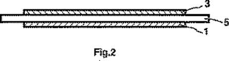
第5工程では、好ましくは機械的分離によって、金属片2および4が取り除かれる。図2に金属片2および4を取り除いた後の組み合わせ品を示す。先の工程までの表面被覆および圧縮条件は最適化されており、第5工程での金属片の機械的分離を容易にする。
In the fifth step, the
図3に示す第6工程では、接続端子として機能する薄膜状の集電体が物理蒸着によって電極上に形成される。厚さ0.2μmの銅層から成る、第1の集電体6は、負極1上に堆積される。厚さ0.2μmのアルミニウム層から成る第2の集電体7は、正極3上に堆積される。
In the sixth step shown in FIG. 3, a thin-film current collector that functions as a connection terminal is formed on the electrode by physical vapor deposition. A first
図4に示す第7工程では、マイクロ電池は集積回路8上に集積される。これは、マイクロエレクトロニクス(フリップチップ、ボンディング、ダイレクトまたはアノードシーリング)の分野では周知の適当な技術を用いて行われる。好ましくは、低い温度で溶融する物質から成る接続ボール9を用いて接続をすることによって集積化が成され、マイクロ電池と集積回路との機械的接続と、集電体の片方(図4では6)と集積回路との電気的接続との両方が成される。好ましくは、接続ボール9はマイクロ電池の材料に対応する融点(157℃)を持つ、インジウムから成る。
In the seventh step shown in FIG. 4, the microbattery is integrated on the integrated circuit 8. This is done using any suitable technique well known in the field of microelectronics (flip chip, bonding, direct or anode sealing). Preferably, the integration is achieved by connecting with
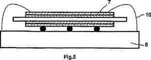
図5に示す第8工程では、接続ボール9によって集積回路8に電気的に接続されていない集電体7が、少なくとも1本のワイヤ10によって集積回路に接続される。ワイヤ10は、一端で集電体7上にハンダづけされ、もう一端で集積回路8にハンダづけされる。
In the eighth step shown in FIG. 5, the current collector 7 that is not electrically connected to the integrated circuit 8 by the
最終工程では、リチウム塩から成る電解質を真空中で充填することによって、マイクロ電池は活性化する。次にマイクロ電池は、例えばシリコン保護キャップによって封止される。 In the final step, the microbattery is activated by filling an electrolyte composed of a lithium salt in a vacuum. The microbattery is then sealed, for example with a silicon protective cap.
このように、上述の製造方法では従来ミニ電池を製造するのに用いられてきた技術(電極と電解質膜とで構成される活性積層体の層の表面被覆)と同様の技術が一部で用いられている。しかし、金属片を分離することにより、この積層体の厚さはかなり減少している。次に、マイクロエレクトロニクスの分野で標準的に行われている、PVDタイプの技術を用いて集電体を堆積することにより、この積層体は完成される。 As described above, in the above-described manufacturing method, a technique similar to the technique (surface coating of the layer of the active laminate composed of the electrode and the electrolyte membrane) that has been conventionally used for manufacturing the mini battery is partially used. It has been. However, by separating the metal pieces, the thickness of this laminate is significantly reduced. The stack is then completed by depositing the current collector using PVD type technology, which is standard practice in the field of microelectronics.
これにより、例えば表面積が25mm2で厚さが50μmであり、表面容量が約500μAh/cm2(すなわち125μAh)、つまり現在のマイクロ電池の5倍も表面容量が大きいマイクロ電池を製造することができる。このマイクロ電池は、自己の充電および放電を管理する集積回路上に実装することができる。このようにして得られたマイクロ電池は、ミニ電池の利点(特に高い表面容量)と、マイクロ電池の利点(集積回路に実装可能)を併せ持つ。このタイプのマイクロ電池は特に、スマートカードやスマートラベルの安全性を向上させるのに用いられる。 Thereby, for example, a micro battery having a surface area of 25 mm 2 and a thickness of 50 μm and a surface capacity of about 500 μAh / cm 2 (ie, 125 μAh), that is, a surface capacity that is five times as large as that of the current micro battery can be manufactured. . The microbattery can be mounted on an integrated circuit that manages its own charging and discharging. The microbattery thus obtained has both the advantages of a mini-battery (particularly high surface capacity) and the advantages of a microbattery (can be mounted on an integrated circuit). This type of microbattery is particularly used to improve the safety of smart cards and smart labels.
図6に示す他の実施形態では、単一の金属片が用いられる。先ほどと同様に、電極の片方、例えば負極1が金属片2上に形成される。次に電解質膜5が負極1上に形成され、もう片方の電極(正極3)が電解質膜5上に直接塗布されることによって形成される。組み合わせ品の熱間圧縮後、金属片2は取り除かれる。このようにして形成された組み合わせ品は、図2に示すものと同様であり、その後の製造工程は変わらない。
In another embodiment shown in FIG. 6, a single piece of metal is used. As before, one side of the electrode, for example, the negative electrode 1 is formed on the
1,3 電極
2,4 金属片
5 電解質膜
6,7 集電体
8 集積回路
9 接続ボール
10 ワイヤ
DESCRIPTION OF
Claims (9)
前記第1電極(1)は、第1の金属片(2)の表面の被覆を行い、次に冷間圧縮を行うことによって前記第1の金属片(2)上に形成され、
前記第2電極(3)は、第2の金属片(4)の表面の被覆を行い、次に冷間圧縮を行うことによって前記第2の金属片(4)上に形成され、
前記第1電極および第2電極(1,3)と、前記電解質膜(5)とは、熱間圧縮によって組み合わせられ、
前記第1の金属片(2)は、前記集電体(6,7)が形成される前に取り除かれ、
前記第2の金属片(4)は、前記集電体(6,7)が形成される前に取り除かれることを特徴とする、リチウムマイクロ電池の製造方法。An electrolyte membrane (5) disposed between the first electrode and the second electrode (1, 3), and a collector disposed on the opposite side of the electrolyte membrane (5) in the first electrode and the second electrode. A method of manufacturing a lithium microbattery comprising an electric body (6, 7),
The first electrode (1) is formed on the first metal piece (2) by covering the surface of the first metal piece (2) and then performing cold compression,
The second electrode (3) is formed on the second metal piece (4) by covering the surface of the second metal piece (4) and then performing cold compression,
The first and second electrodes (1, 3) and the electrolyte membrane (5) are combined by hot compression,
The first metal piece (2) is removed before the current collector (6, 7) is formed;
The method of manufacturing a lithium micro battery, wherein the second metal piece (4) is removed before the current collector (6, 7) is formed .
前記第1電極(1)は、第1の金属片(2)の表面の被覆を行い、次に冷間圧縮を行うことによって前記第1の金属片(2)上に形成され、
前記第2電極(3)は、表面被覆によって前記電解質膜(5)上に形成され、
前記第1電極および第2電極(1,3)と、前記電解質膜(5)とは、熱間圧縮によって組み合わせられ、
前記第1の金属片(2)は、前記集電体(6,7)が形成される前に取り除かれることを特徴とする、リチウムマイクロ電池の製造方法。An electrolyte membrane (5) disposed between the first electrode and the second electrode (1, 3), and a collector disposed on the opposite side of the electrolyte membrane (5) in the first electrode and the second electrode. A method of manufacturing a lithium microbattery comprising an electric body (6, 7),
The first electrode (1) is formed on the first metal piece (2) by covering the surface of the first metal piece (2) and then performing cold compression,
The second electrode (3) is formed on the electrolyte membrane (5) by surface coating,
The first and second electrodes (1, 3) and the electrolyte membrane (5) are combined by hot compression,
The method of manufacturing a lithium micro battery, wherein the first metal piece (2) is removed before the current collector (6, 7) is formed.
Applications Claiming Priority (2)
| Application Number | Priority Date | Filing Date | Title |
|---|---|---|---|
| FR0113570A FR2831331B1 (en) | 2001-10-22 | 2001-10-22 | METHOD FOR MANUFACTURING A MICRO-BATTERY |
| PCT/FR2002/003590 WO2003036750A1 (en) | 2001-10-22 | 2002-10-21 | Method for making a micro-battery |
Publications (2)
| Publication Number | Publication Date |
|---|---|
| JP2005506677A JP2005506677A (en) | 2005-03-03 |
| JP4639376B2 true JP4639376B2 (en) | 2011-02-23 |
Family
ID=8868533
Family Applications (1)
| Application Number | Title | Priority Date | Filing Date |
|---|---|---|---|
| JP2003539126A Expired - Fee Related JP4639376B2 (en) | 2001-10-22 | 2002-10-21 | Method for producing lithium micro battery |
Country Status (6)
| Country | Link |
|---|---|
| US (1) | US7235112B2 (en) |
| EP (1) | EP1438763A1 (en) |
| JP (1) | JP4639376B2 (en) |
| CN (1) | CN1263190C (en) |
| FR (1) | FR2831331B1 (en) |
| WO (1) | WO2003036750A1 (en) |
Families Citing this family (24)
| Publication number | Priority date | Publication date | Assignee | Title |
|---|---|---|---|---|
| US8511684B2 (en) | 2004-10-04 | 2013-08-20 | Shfl Entertainment, Inc. | Card-reading shoe with inventory correction feature and methods of correcting inventory |
| WO2004090982A1 (en) * | 2003-04-04 | 2004-10-21 | Matsushita Electric Industrial Co., Ltd. | Battery-mounted integrated circuit device |
| FR2880198B1 (en) * | 2004-12-23 | 2007-07-06 | Commissariat Energie Atomique | NANOSTRUCTURED ELECTRODE FOR MICROBATTERY |
| US7776478B2 (en) | 2005-07-15 | 2010-08-17 | Cymbet Corporation | Thin-film batteries with polymer and LiPON electrolyte layers and method |
| JP2009502011A (en) * | 2005-07-15 | 2009-01-22 | シンベット・コーポレイション | Thin film battery and method with soft and hard electrolyte layers |
| US7884720B2 (en) | 2005-08-01 | 2011-02-08 | Powerid Ltd. | Intermediate attachment mechanism and use thereof in RFID transponder |
| TWI419397B (en) * | 2006-05-12 | 2013-12-11 | Infinite Power Solutions Inc | Thin film battery on a semiconductor or semiconductor device apparatus and method |
| FR2901639B1 (en) * | 2006-05-24 | 2008-08-22 | Commissariat Energie Atomique | INTEGRATED MICRO COMPONENT ASSOCIATING THE RECOVERY AND STORAGE FUNCTIONS OF ENERGY |
| GB0621738D0 (en) * | 2006-10-31 | 2006-12-13 | Nanotecture Ltd | Electrochemical cell for use in smart cards |
| DE102008004308A1 (en) * | 2008-01-15 | 2009-07-16 | Biotronik Crm Patent Ag | Implementation for a battery, method of making the same and battery |
| DE102008018172A1 (en) * | 2008-04-03 | 2009-10-08 | Varta Microbattery Gmbh | Galvanic cell and process for its preparation |
| JP5255978B2 (en) * | 2008-10-16 | 2013-08-07 | トヨタ自動車株式会社 | Solid battery manufacturing method |
| JP5255979B2 (en) * | 2008-10-16 | 2013-08-07 | トヨタ自動車株式会社 | Solid battery manufacturing method |
| FR2954588B1 (en) * | 2009-12-23 | 2014-07-25 | Commissariat Energie Atomique | METHOD FOR ASSEMBLING AT LEAST ONE CHIP WITH A WIRED ELEMENT, ELECTRONIC CHIP WITH DEFORMABLE BONDING ELEMENT, METHOD FOR MANUFACTURING A PLURALITY OF CHIPS, AND ASSEMBLY OF AT LEAST ONE CHIP WITH A WIRED ELEMENT |
| FR2961638B1 (en) * | 2010-06-21 | 2012-07-06 | Commissariat Energie Atomique | MICROBATTERY AND PROCESS FOR PRODUCING MICROBATTERY |
| KR101218215B1 (en) * | 2010-12-28 | 2013-01-03 | 지에스나노텍 주식회사 | Thin film battery package |
| US11527774B2 (en) | 2011-06-29 | 2022-12-13 | Space Charge, LLC | Electrochemical energy storage devices |
| US11996517B2 (en) | 2011-06-29 | 2024-05-28 | Space Charge, LLC | Electrochemical energy storage devices |
| US9853325B2 (en) | 2011-06-29 | 2017-12-26 | Space Charge, LLC | Rugged, gel-free, lithium-free, high energy density solid-state electrochemical energy storage devices |
| US10601074B2 (en) | 2011-06-29 | 2020-03-24 | Space Charge, LLC | Rugged, gel-free, lithium-free, high energy density solid-state electrochemical energy storage devices |
| FR3059158A1 (en) | 2016-11-18 | 2018-05-25 | Universite De Tours Francois Rabelais | ACHIEVEMENT OF 3D BATTERIES BY LIQUID WAY |
| US10950912B2 (en) | 2017-06-14 | 2021-03-16 | Milwaukee Electric Tool Corporation | Arrangements for inhibiting intrusion into battery pack electrical components |
| US10749199B2 (en) | 2017-11-29 | 2020-08-18 | International Business Machines Corporation | Li1+xAlxTi2-x(PO4)3 solid-state thin film electrolyte for 3D microbattery and method of fabrication |
| EP3762989A4 (en) | 2018-03-07 | 2021-12-15 | Space Charge, LLC | Thin-film solid-state energy-storage devices |
Family Cites Families (15)
| Publication number | Priority date | Publication date | Assignee | Title |
|---|---|---|---|---|
| FR1575553A (en) * | 1967-12-08 | 1969-07-25 | ||
| US5154784A (en) * | 1991-02-01 | 1992-10-13 | Westinghouse Electric Corp. | Process for manufacturing a lithium alloy electrochemical cell |
| FR2727227B1 (en) * | 1994-11-17 | 1996-12-20 | Schlumberger Ind Sa | ACTIVE SECURITY DEVICE WITH ELECTRONIC MEMORY |
| US5582623A (en) * | 1994-11-23 | 1996-12-10 | Polyplus Battery Company, Inc. | Methods of fabricating rechargeable positive electrodes |
| TW399029B (en) * | 1996-12-25 | 2000-07-21 | Sony Corp | Graphite powder suitable for negative electrode material of lithium ion secondary batteries |
| US6030421A (en) * | 1997-04-23 | 2000-02-29 | Hydro-Quebec | Ultra thin solid state lithium batteries and process of preparing same |
| US5978230A (en) * | 1998-02-19 | 1999-11-02 | Micron Communications, Inc. | Battery mounting apparatuses, electronic devices, and methods of forming electrical connections |
| JPH11260355A (en) * | 1998-03-10 | 1999-09-24 | Tdk Corp | Manufacture of electrochemical element |
| US6610440B1 (en) * | 1998-03-10 | 2003-08-26 | Bipolar Technologies, Inc | Microscopic batteries for MEMS systems |
| AU5731400A (en) * | 1999-06-09 | 2000-12-28 | Moltech Corporation | Methods of preparing electrochemical cells |
| JP2001052753A (en) * | 1999-08-04 | 2001-02-23 | Nissan Motor Co Ltd | Battery and its manufacture |
| JP4845244B2 (en) * | 1999-10-25 | 2011-12-28 | 京セラ株式会社 | Lithium battery |
| JP4157999B2 (en) * | 1999-11-09 | 2008-10-01 | ソニー株式会社 | Electrode and gel electrolyte battery manufacturing method |
| US6402796B1 (en) * | 2000-08-07 | 2002-06-11 | Excellatron Solid State, Llc | Method of producing a thin film battery |
| JP2003243038A (en) * | 2002-02-19 | 2003-08-29 | Matsushita Electric Ind Co Ltd | Positive electrode plate and lithium secondary battery using it |
-
2001
- 2001-10-22 FR FR0113570A patent/FR2831331B1/en not_active Expired - Fee Related
-
2002
- 2002-10-21 JP JP2003539126A patent/JP4639376B2/en not_active Expired - Fee Related
- 2002-10-21 EP EP02790526A patent/EP1438763A1/en not_active Withdrawn
- 2002-10-21 US US10/250,903 patent/US7235112B2/en not_active Expired - Lifetime
- 2002-10-21 CN CNB028061225A patent/CN1263190C/en not_active Expired - Fee Related
- 2002-10-21 WO PCT/FR2002/003590 patent/WO2003036750A1/en active Application Filing
Also Published As
| Publication number | Publication date |
|---|---|
| CN1496591A (en) | 2004-05-12 |
| US7235112B2 (en) | 2007-06-26 |
| JP2005506677A (en) | 2005-03-03 |
| WO2003036750A1 (en) | 2003-05-01 |
| EP1438763A1 (en) | 2004-07-21 |
| CN1263190C (en) | 2006-07-05 |
| US20040049909A1 (en) | 2004-03-18 |
| FR2831331B1 (en) | 2004-11-19 |
| FR2831331A1 (en) | 2003-04-25 |
Similar Documents
| Publication | Publication Date | Title |
|---|---|---|
| JP4639376B2 (en) | Method for producing lithium micro battery | |
| US9590277B2 (en) | Power storage device and manufacturing method thereof | |
| US8790801B2 (en) | Integrated electrochemical and solar cell | |
| JP5235334B2 (en) | Integrated micro components that combine energy recovery and storage functions | |
| US8431264B2 (en) | Hybrid thin-film battery | |
| US6187061B1 (en) | Supercapacitor structure and method of making same | |
| US20090136839A1 (en) | Thin film battery comprising stacked battery cells and method | |
| KR101146616B1 (en) | Thin film battery and method of connecting electrode terminal of thin film battery | |
| US20190165342A1 (en) | Thin-film battery with adhesive layer | |
| JP7065944B2 (en) | Laminated Battery Structures and Methods for Manufacturing Laminated Battery Structures | |
| US20110070480A1 (en) | Three-dimensional microbattery and method for the production thereof | |
| JP2005507544A (en) | Thin-film rapid charge energy storage device | |
| JP2008509512A (en) | Microbattery provided with through connection body and manufacturing method thereof | |
| JP2004127743A (en) | Thin film battery | |
| JP2016058335A (en) | All-solid battery, manufacturing method thereof, and method for recovering capacity | |
| JP2014517457A (en) | Architecture with storage and / or stacking of electrical energy generating elements with configurable electrical output and method of making such an architecture | |
| JP2001043893A (en) | Whole solid secondary battery and its manufacture | |
| JP4381176B2 (en) | Thin film solid secondary battery | |
| JP2000138057A (en) | Solid electrolyte battery its manufacture | |
| JP4283518B2 (en) | Electrochemical devices | |
| JP4202549B2 (en) | Electrochemical device and manufacturing method thereof | |
| JP2004234880A (en) | Laminated battery | |
| JP2003242958A (en) | Lithium cell | |
| JP2010080210A (en) | Battery and method for manufacturing the same | |
| JP2004179090A (en) | Layered battery |
Legal Events
| Date | Code | Title | Description |
|---|---|---|---|
| A621 | Written request for application examination |
Free format text: JAPANESE INTERMEDIATE CODE: A621 Effective date: 20050921 |
|
| A131 | Notification of reasons for refusal |
Free format text: JAPANESE INTERMEDIATE CODE: A131 Effective date: 20090206 |
|
| A521 | Request for written amendment filed |
Free format text: JAPANESE INTERMEDIATE CODE: A523 Effective date: 20090507 |
|
| A131 | Notification of reasons for refusal |
Free format text: JAPANESE INTERMEDIATE CODE: A131 Effective date: 20090602 |
|
| A521 | Request for written amendment filed |
Free format text: JAPANESE INTERMEDIATE CODE: A523 Effective date: 20090826 |
|
| A02 | Decision of refusal |
Free format text: JAPANESE INTERMEDIATE CODE: A02 Effective date: 20100202 |
|
| A521 | Request for written amendment filed |
Free format text: JAPANESE INTERMEDIATE CODE: A523 Effective date: 20100602 |
|
| A911 | Transfer to examiner for re-examination before appeal (zenchi) |
Free format text: JAPANESE INTERMEDIATE CODE: A911 Effective date: 20100729 |
|
| TRDD | Decision of grant or rejection written | ||
| A01 | Written decision to grant a patent or to grant a registration (utility model) |
Free format text: JAPANESE INTERMEDIATE CODE: A01 Effective date: 20101012 |
|
| A01 | Written decision to grant a patent or to grant a registration (utility model) |
Free format text: JAPANESE INTERMEDIATE CODE: A01 |
|
| A61 | First payment of annual fees (during grant procedure) |
Free format text: JAPANESE INTERMEDIATE CODE: A61 Effective date: 20101110 |
|
| R150 | Certificate of patent or registration of utility model |
Free format text: JAPANESE INTERMEDIATE CODE: R150 |
|
| FPAY | Renewal fee payment (event date is renewal date of database) |
Free format text: PAYMENT UNTIL: 20131210 Year of fee payment: 3 |
|
| R250 | Receipt of annual fees |
Free format text: JAPANESE INTERMEDIATE CODE: R250 |
|
| R250 | Receipt of annual fees |
Free format text: JAPANESE INTERMEDIATE CODE: R250 |
|
| LAPS | Cancellation because of no payment of annual fees |