JP4636626B2 - Liquid crystal display element - Google Patents
Liquid crystal display element Download PDFInfo
- Publication number
- JP4636626B2 JP4636626B2 JP2008100196A JP2008100196A JP4636626B2 JP 4636626 B2 JP4636626 B2 JP 4636626B2 JP 2008100196 A JP2008100196 A JP 2008100196A JP 2008100196 A JP2008100196 A JP 2008100196A JP 4636626 B2 JP4636626 B2 JP 4636626B2
- Authority
- JP
- Japan
- Prior art keywords
- liquid crystal
- array substrate
- counter
- electrode
- layer
- Prior art date
- Legal status (The legal status is an assumption and is not a legal conclusion. Google has not performed a legal analysis and makes no representation as to the accuracy of the status listed.)
- Active
Links
- 239000004973 liquid crystal related substance Substances 0.000 title claims description 104
- 239000000758 substrate Substances 0.000 claims description 104
- GWEVSGVZZGPLCZ-UHFFFAOYSA-N Titan oxide Chemical compound O=[Ti]=O GWEVSGVZZGPLCZ-UHFFFAOYSA-N 0.000 claims description 20
- 230000005540 biological transmission Effects 0.000 claims description 20
- OGIDPMRJRNCKJF-UHFFFAOYSA-N titanium oxide Inorganic materials [Ti]=O OGIDPMRJRNCKJF-UHFFFAOYSA-N 0.000 claims description 20
- 150000001875 compounds Chemical class 0.000 claims description 12
- 238000009413 insulation Methods 0.000 claims description 2
- 239000010410 layer Substances 0.000 description 74
- 239000010408 film Substances 0.000 description 59
- 238000002834 transmittance Methods 0.000 description 18
- 210000002858 crystal cell Anatomy 0.000 description 14
- 230000005684 electric field Effects 0.000 description 12
- 239000011521 glass Substances 0.000 description 10
- 238000000034 method Methods 0.000 description 10
- 230000000052 comparative effect Effects 0.000 description 9
- 239000011347 resin Substances 0.000 description 9
- 229920005989 resin Polymers 0.000 description 9
- 239000010409 thin film Substances 0.000 description 9
- 230000000694 effects Effects 0.000 description 8
- 239000000463 material Substances 0.000 description 7
- 239000004065 semiconductor Substances 0.000 description 7
- 230000007423 decrease Effects 0.000 description 6
- 230000008569 process Effects 0.000 description 6
- 230000001681 protective effect Effects 0.000 description 6
- 238000000206 photolithography Methods 0.000 description 5
- 125000006850 spacer group Chemical group 0.000 description 5
- 229910052581 Si3N4 Inorganic materials 0.000 description 4
- 229910021417 amorphous silicon Inorganic materials 0.000 description 4
- 238000002347 injection Methods 0.000 description 4
- 239000007924 injection Substances 0.000 description 4
- 230000004044 response Effects 0.000 description 4
- HQVNEWCFYHHQES-UHFFFAOYSA-N silicon nitride Chemical compound N12[Si]34N5[Si]62N3[Si]51N64 HQVNEWCFYHHQES-UHFFFAOYSA-N 0.000 description 4
- 230000015572 biosynthetic process Effects 0.000 description 3
- 230000001276 controlling effect Effects 0.000 description 3
- 238000005530 etching Methods 0.000 description 3
- ZOKXTWBITQBERF-UHFFFAOYSA-N Molybdenum Chemical compound [Mo] ZOKXTWBITQBERF-UHFFFAOYSA-N 0.000 description 2
- 239000004988 Nematic liquid crystal Substances 0.000 description 2
- VYPSYNLAJGMNEJ-UHFFFAOYSA-N Silicium dioxide Chemical compound O=[Si]=O VYPSYNLAJGMNEJ-UHFFFAOYSA-N 0.000 description 2
- NIXOWILDQLNWCW-UHFFFAOYSA-N acrylic acid group Chemical group C(C=C)(=O)O NIXOWILDQLNWCW-UHFFFAOYSA-N 0.000 description 2
- 239000000853 adhesive Substances 0.000 description 2
- 230000001070 adhesive effect Effects 0.000 description 2
- 239000004020 conductor Substances 0.000 description 2
- 230000002349 favourable effect Effects 0.000 description 2
- AMGQUBHHOARCQH-UHFFFAOYSA-N indium;oxotin Chemical compound [In].[Sn]=O AMGQUBHHOARCQH-UHFFFAOYSA-N 0.000 description 2
- 229910052750 molybdenum Inorganic materials 0.000 description 2
- 239000011733 molybdenum Substances 0.000 description 2
- 238000000016 photochemical curing Methods 0.000 description 2
- 229910052814 silicon oxide Inorganic materials 0.000 description 2
- 238000004544 sputter deposition Methods 0.000 description 2
- 239000004593 Epoxy Substances 0.000 description 1
- 239000004990 Smectic liquid crystal Substances 0.000 description 1
- PSLUFJFHTBIXMW-WYEYVKMPSA-N [(3r,4ar,5s,6s,6as,10s,10ar,10bs)-3-ethenyl-10,10b-dihydroxy-3,4a,7,7,10a-pentamethyl-1-oxo-6-(2-pyridin-2-ylethylcarbamoyloxy)-5,6,6a,8,9,10-hexahydro-2h-benzo[f]chromen-5-yl] acetate Chemical compound O([C@@H]1[C@@H]([C@]2(O[C@](C)(CC(=O)[C@]2(O)[C@@]2(C)[C@@H](O)CCC(C)(C)[C@@H]21)C=C)C)OC(=O)C)C(=O)NCCC1=CC=CC=N1 PSLUFJFHTBIXMW-WYEYVKMPSA-N 0.000 description 1
- 238000010521 absorption reaction Methods 0.000 description 1
- 229910052782 aluminium Inorganic materials 0.000 description 1
- XAGFODPZIPBFFR-UHFFFAOYSA-N aluminium Chemical compound [Al] XAGFODPZIPBFFR-UHFFFAOYSA-N 0.000 description 1
- 230000015556 catabolic process Effects 0.000 description 1
- 230000008859 change Effects 0.000 description 1
- 230000007547 defect Effects 0.000 description 1
- 238000010586 diagram Methods 0.000 description 1
- 238000011156 evaluation Methods 0.000 description 1
- 230000001747 exhibiting effect Effects 0.000 description 1
- 239000005262 ferroelectric liquid crystals (FLCs) Substances 0.000 description 1
- 230000008570 general process Effects 0.000 description 1
- 230000006872 improvement Effects 0.000 description 1
- 238000004519 manufacturing process Methods 0.000 description 1
- 239000011159 matrix material Substances 0.000 description 1
- 230000003287 optical effect Effects 0.000 description 1
- 239000012044 organic layer Substances 0.000 description 1
- 238000000059 patterning Methods 0.000 description 1
- 230000035699 permeability Effects 0.000 description 1
- 239000011241 protective layer Substances 0.000 description 1
- 239000001054 red pigment Substances 0.000 description 1
- 230000001105 regulatory effect Effects 0.000 description 1
- 230000004043 responsiveness Effects 0.000 description 1
- 238000007789 sealing Methods 0.000 description 1
- 239000003566 sealing material Substances 0.000 description 1
- 229920001187 thermosetting polymer Polymers 0.000 description 1
Images


Classifications
-
- G—PHYSICS
- G02—OPTICS
- G02F—OPTICAL DEVICES OR ARRANGEMENTS FOR THE CONTROL OF LIGHT BY MODIFICATION OF THE OPTICAL PROPERTIES OF THE MEDIA OF THE ELEMENTS INVOLVED THEREIN; NON-LINEAR OPTICS; FREQUENCY-CHANGING OF LIGHT; OPTICAL LOGIC ELEMENTS; OPTICAL ANALOGUE/DIGITAL CONVERTERS
- G02F1/00—Devices or arrangements for the control of the intensity, colour, phase, polarisation or direction of light arriving from an independent light source, e.g. switching, gating or modulating; Non-linear optics
- G02F1/01—Devices or arrangements for the control of the intensity, colour, phase, polarisation or direction of light arriving from an independent light source, e.g. switching, gating or modulating; Non-linear optics for the control of the intensity, phase, polarisation or colour
- G02F1/13—Devices or arrangements for the control of the intensity, colour, phase, polarisation or direction of light arriving from an independent light source, e.g. switching, gating or modulating; Non-linear optics for the control of the intensity, phase, polarisation or colour based on liquid crystals, e.g. single liquid crystal display cells
- G02F1/133—Constructional arrangements; Operation of liquid crystal cells; Circuit arrangements
- G02F1/1333—Constructional arrangements; Manufacturing methods
- G02F1/1337—Surface-induced orientation of the liquid crystal molecules, e.g. by alignment layers
- G02F1/133707—Structures for producing distorted electric fields, e.g. bumps, protrusions, recesses, slits in pixel electrodes
-
- G—PHYSICS
- G02—OPTICS
- G02F—OPTICAL DEVICES OR ARRANGEMENTS FOR THE CONTROL OF LIGHT BY MODIFICATION OF THE OPTICAL PROPERTIES OF THE MEDIA OF THE ELEMENTS INVOLVED THEREIN; NON-LINEAR OPTICS; FREQUENCY-CHANGING OF LIGHT; OPTICAL LOGIC ELEMENTS; OPTICAL ANALOGUE/DIGITAL CONVERTERS
- G02F1/00—Devices or arrangements for the control of the intensity, colour, phase, polarisation or direction of light arriving from an independent light source, e.g. switching, gating or modulating; Non-linear optics
- G02F1/01—Devices or arrangements for the control of the intensity, colour, phase, polarisation or direction of light arriving from an independent light source, e.g. switching, gating or modulating; Non-linear optics for the control of the intensity, phase, polarisation or colour
- G02F1/13—Devices or arrangements for the control of the intensity, colour, phase, polarisation or direction of light arriving from an independent light source, e.g. switching, gating or modulating; Non-linear optics for the control of the intensity, phase, polarisation or colour based on liquid crystals, e.g. single liquid crystal display cells
- G02F1/133—Constructional arrangements; Operation of liquid crystal cells; Circuit arrangements
- G02F1/1333—Constructional arrangements; Manufacturing methods
- G02F1/1337—Surface-induced orientation of the liquid crystal molecules, e.g. by alignment layers
- G02F1/133742—Surface-induced orientation of the liquid crystal molecules, e.g. by alignment layers for homeotropic alignment
-
- G—PHYSICS
- G02—OPTICS
- G02F—OPTICAL DEVICES OR ARRANGEMENTS FOR THE CONTROL OF LIGHT BY MODIFICATION OF THE OPTICAL PROPERTIES OF THE MEDIA OF THE ELEMENTS INVOLVED THEREIN; NON-LINEAR OPTICS; FREQUENCY-CHANGING OF LIGHT; OPTICAL LOGIC ELEMENTS; OPTICAL ANALOGUE/DIGITAL CONVERTERS
- G02F1/00—Devices or arrangements for the control of the intensity, colour, phase, polarisation or direction of light arriving from an independent light source, e.g. switching, gating or modulating; Non-linear optics
- G02F1/01—Devices or arrangements for the control of the intensity, colour, phase, polarisation or direction of light arriving from an independent light source, e.g. switching, gating or modulating; Non-linear optics for the control of the intensity, phase, polarisation or colour
- G02F1/13—Devices or arrangements for the control of the intensity, colour, phase, polarisation or direction of light arriving from an independent light source, e.g. switching, gating or modulating; Non-linear optics for the control of the intensity, phase, polarisation or colour based on liquid crystals, e.g. single liquid crystal display cells
- G02F1/133—Constructional arrangements; Operation of liquid crystal cells; Circuit arrangements
- G02F1/1333—Constructional arrangements; Manufacturing methods
- G02F1/1343—Electrodes
- G02F1/134309—Electrodes characterised by their geometrical arrangement
- G02F1/134318—Electrodes characterised by their geometrical arrangement having a patterned common electrode
-
- G—PHYSICS
- G02—OPTICS
- G02F—OPTICAL DEVICES OR ARRANGEMENTS FOR THE CONTROL OF LIGHT BY MODIFICATION OF THE OPTICAL PROPERTIES OF THE MEDIA OF THE ELEMENTS INVOLVED THEREIN; NON-LINEAR OPTICS; FREQUENCY-CHANGING OF LIGHT; OPTICAL LOGIC ELEMENTS; OPTICAL ANALOGUE/DIGITAL CONVERTERS
- G02F1/00—Devices or arrangements for the control of the intensity, colour, phase, polarisation or direction of light arriving from an independent light source, e.g. switching, gating or modulating; Non-linear optics
- G02F1/01—Devices or arrangements for the control of the intensity, colour, phase, polarisation or direction of light arriving from an independent light source, e.g. switching, gating or modulating; Non-linear optics for the control of the intensity, phase, polarisation or colour
- G02F1/13—Devices or arrangements for the control of the intensity, colour, phase, polarisation or direction of light arriving from an independent light source, e.g. switching, gating or modulating; Non-linear optics for the control of the intensity, phase, polarisation or colour based on liquid crystals, e.g. single liquid crystal display cells
- G02F1/133—Constructional arrangements; Operation of liquid crystal cells; Circuit arrangements
- G02F1/1333—Constructional arrangements; Manufacturing methods
- G02F1/1343—Electrodes
- G02F1/134309—Electrodes characterised by their geometrical arrangement
- G02F1/134381—Hybrid switching mode, i.e. for applying an electric field with components parallel and orthogonal to the substrates
-
- G—PHYSICS
- G02—OPTICS
- G02F—OPTICAL DEVICES OR ARRANGEMENTS FOR THE CONTROL OF LIGHT BY MODIFICATION OF THE OPTICAL PROPERTIES OF THE MEDIA OF THE ELEMENTS INVOLVED THEREIN; NON-LINEAR OPTICS; FREQUENCY-CHANGING OF LIGHT; OPTICAL LOGIC ELEMENTS; OPTICAL ANALOGUE/DIGITAL CONVERTERS
- G02F2201/00—Constructional arrangements not provided for in groups G02F1/00 - G02F7/00
- G02F2201/12—Constructional arrangements not provided for in groups G02F1/00 - G02F7/00 electrode
- G02F2201/123—Constructional arrangements not provided for in groups G02F1/00 - G02F7/00 electrode pixel
-
- G—PHYSICS
- G02—OPTICS
- G02F—OPTICAL DEVICES OR ARRANGEMENTS FOR THE CONTROL OF LIGHT BY MODIFICATION OF THE OPTICAL PROPERTIES OF THE MEDIA OF THE ELEMENTS INVOLVED THEREIN; NON-LINEAR OPTICS; FREQUENCY-CHANGING OF LIGHT; OPTICAL LOGIC ELEMENTS; OPTICAL ANALOGUE/DIGITAL CONVERTERS
- G02F2201/00—Constructional arrangements not provided for in groups G02F1/00 - G02F7/00
- G02F2201/12—Constructional arrangements not provided for in groups G02F1/00 - G02F7/00 electrode
- G02F2201/128—Constructional arrangements not provided for in groups G02F1/00 - G02F7/00 electrode field shaping
-
- G—PHYSICS
- G02—OPTICS
- G02F—OPTICAL DEVICES OR ARRANGEMENTS FOR THE CONTROL OF LIGHT BY MODIFICATION OF THE OPTICAL PROPERTIES OF THE MEDIA OF THE ELEMENTS INVOLVED THEREIN; NON-LINEAR OPTICS; FREQUENCY-CHANGING OF LIGHT; OPTICAL LOGIC ELEMENTS; OPTICAL ANALOGUE/DIGITAL CONVERTERS
- G02F2202/00—Materials and properties
- G02F2202/42—Materials having a particular dielectric constant
Landscapes
- Physics & Mathematics (AREA)
- Nonlinear Science (AREA)
- Spectroscopy & Molecular Physics (AREA)
- Mathematical Physics (AREA)
- Chemical & Material Sciences (AREA)
- Crystallography & Structural Chemistry (AREA)
- General Physics & Mathematics (AREA)
- Optics & Photonics (AREA)
- Liquid Crystal (AREA)
Description
本発明は、液晶層を画素電極と対向電極との間の電圧印加時の液晶分子の倒れ方向が互いに異なる複数のドメインに分割する液晶表示素子に関する。 The present invention relates to a liquid crystal display element that divides a liquid crystal layer into a plurality of domains in which liquid crystal molecules fall in different directions when a voltage is applied between a pixel electrode and a counter electrode.
液晶素子を用いた表示装置は、軽量、薄型、低消費電力などの特徴を有するために、OA機器、情報端末、時計、テレビジョン受像機など、さまざまな分野に応用されている。特に薄膜トランジスタ(TFT素子)を用いた液晶素子は、その応答性から携帯テレビやコンピュータなど多くの情報を含むデータの表示用モニタなどに用いられている。 Display devices using liquid crystal elements have features such as light weight, thinness, and low power consumption, and thus are applied to various fields such as OA equipment, information terminals, watches, and television receivers. In particular, a liquid crystal element using a thin film transistor (TFT element) is used for a display monitor of data including a lot of information such as a portable television and a computer because of its responsiveness.
近年、情報量の増加や動画表示の増加に伴い、高精細化や高速応答性、広視角特性が要求され始めており、高精細化にはTFTアレイ構造の微細化により対応がなされている。 In recent years, with the increase in the amount of information and the increase in moving image display, high definition, high-speed response, and wide viewing angle characteristics have been demanded, and high definition has been dealt with by miniaturization of the TFT array structure.
高速応答性では、例えばネマチック液晶を用いたOCBモード、VANモード、HANモード、π配列モード、スメクチック液晶を用いた界面安定型強誘電性液晶(SSFLC)モード、あるいは反強誘電性液晶(AFLC)モードなどが検討されている。 In high-speed response, for example, OCB mode using nematic liquid crystal, VAN mode, HAN mode, π-alignment mode, interface stable ferroelectric liquid crystal (SSFLC) mode using smectic liquid crystal, or antiferroelectric liquid crystal (AFLC) Modes are being considered.
さらに、広視角特性についても、IPSモード、VANモードやOCBモードといった液晶の駆動方法の工夫により改善がなされてきた。 Furthermore, wide viewing angle characteristics have also been improved by devising liquid crystal driving methods such as IPS mode, VAN mode, and OCB mode.
特に、VANモードは、従来のツイストネマチック(TN)モードより速い応答速度が得られることや、垂直配向処理の採用により、従来静電気破壊など不良原因の発生が危惧されていたラビング配向処理工程を削除可能なことから近年注目されている。さらに、視野角の補償設計が比較的容易なことから、マルチドメイン型VANモード(以下、MVAモードという)として広い視野角を実現することが可能である。 In particular, in the VAN mode, the rubbing alignment process step, which has been concerned about the occurrence of defects such as electrostatic breakdown, has been eliminated by the fact that a faster response speed than the conventional twisted nematic (TN) mode can be obtained and the vertical alignment process is adopted. It has been attracting attention in recent years because it is possible. Furthermore, since the viewing angle compensation design is relatively easy, a wide viewing angle can be realized as a multi-domain VAN mode (hereinafter referred to as MVA mode).
MVAモードにおける配向分割のための手段として、一方あるいは両方の基板上に畝状の構造体(突起)あるいは画素電極の欠落部(スリット)などを形成する構成が知られている。そして、負の誘電率異方性を示すネマチック液晶材料を用いる場合、画素電極のスリットでは電界離散効果により電界がスリット内側に傾斜し、液晶分子すなわちダイレクタはスリットの外側に傾斜する。一方で、対向基板側では突起の形状効果によりダイレクタは突起の外側に傾斜する。そこで、ダイレクタの傾斜方向が揃うように両基板を組み合わせることで良好に配向分割を行うことができる。また、例えばアレイ基板側のスリットおよび対向基板側の突起を、基板端辺に対し略45°の角度でかつ互いに略90°異なる4方向への異方性を有するように形成するなど、スリットパターンや突起パターンに複数の異なる方向への異方性を持たせることで、液晶層を複数のドメインに分割することも可能である(例えば、特許文献1参照。)。
上述のように、MVAモードは、高コントラスト比で、広視角なディスプレイとして優れた特徴を有するが、更なるコントラスト比の向上が求められている。 As described above, the MVA mode has excellent characteristics as a display with a high contrast ratio and a wide viewing angle, but further improvement in the contrast ratio is required.
MVAモードのコントラスト比向上の方法として、配向規制手段は畝状の突起構造よりもスリット構造が好ましく、さらにそれらの面積を可能な限り小さくすることが好ましいことがわかっている。これは、高コントラスト比を得るためには黒表示時の輝度を低下させることが重要であるからである。すなわち、MVAモードでは、ダイレクタが基板面に垂直に配向しており位相差すなわち複屈折率Δnが0であるため、アレイ基板と対向基板との上に偏光板を、それぞれの透過軸が直交するように貼り着けた液晶ディスプレイでは、黒表示時の透過光が0に近い値となり高コントラスト比が得られるものの、畝状の突起上に位置するダイレクタは突起の斜面に垂直に、すなわち傾斜状に配向しているため、複屈折率Δnが0とならず、弱い光漏れが生じる。一方で、画素電極のスリット構造では突起がないために、高コントラスト比が得られる。 As a method for improving the contrast ratio of the MVA mode, it has been found that the orientation regulating means preferably has a slit structure rather than a saddle-like protrusion structure, and further it is preferable to make their area as small as possible. This is because it is important to reduce the luminance during black display in order to obtain a high contrast ratio. That is, in the MVA mode, the director is oriented perpendicular to the substrate surface and the phase difference, that is, the birefringence Δn is 0. Therefore, the polarizing plate is placed on the array substrate and the counter substrate, and the transmission axes are orthogonal to each other. In the liquid crystal display thus attached, the transmitted light during black display becomes a value close to 0 and a high contrast ratio is obtained, but the director located on the bowl-shaped projection is perpendicular to the slope of the projection, that is, inclined. Since it is oriented, the birefringence Δn does not become 0 and weak light leakage occurs. On the other hand, since there is no protrusion in the slit structure of the pixel electrode, a high contrast ratio can be obtained.
しかしながら、畝状の突起に比べ画素電極のスリットはダイレクタの配向規制力が弱く、それらの面積が小さくなるほど弱くなる。そのため、例えば白表示時にディスプレイ表面を指で押さえた場合、ダイレクタの配向乱れを生じやすくなるといった欠点を持つ。したがって、画素電極のスリット構造を採用する場合には、そのスリット数を多くせざるを得ない。 However, the slits of the pixel electrodes are weaker than the hook-shaped protrusions, and become weaker as their area becomes smaller. For this reason, for example, when the display surface is pressed with a finger during white display, the director is liable to be disturbed in orientation. Therefore, when the slit structure of the pixel electrode is adopted, the number of slits must be increased.
また、直線偏光モードの液晶表示素子にスリット構造を採用した場合の別の問題として、透過率の低下がある。MVAモードは光の透過制御に液晶の複屈折を利用しており、透過光強度Iは、I0を入射光強度、θを偏光板の透過軸(吸収軸)とダイレクタとのなす角、Δnを液晶の複屈折率、dを液晶層の厚さ、λを光の波長としたとき、次の式(1)で表される。 Another problem when a slit structure is employed in a linearly polarized liquid crystal display element is a decrease in transmittance. The MVA mode uses the birefringence of liquid crystal for light transmission control. The transmitted light intensity I is the incident light intensity I 0 , θ is the angle between the transmission axis (absorption axis) of the polarizer and the director, Δn Is the liquid crystal birefringence, d is the thickness of the liquid crystal layer, and λ is the wavelength of light.
I=I0・sin22θ・sin2(Δn・d・π/λ)……(1) I = I 0 · sin 2 2θ · sin 2 (Δn · d · π / λ) (1)
この式(1)に示す通り、液晶のダイレクタと偏光板の透過軸とのなす角が45°で倒れ角が大きい時、入射光強度I0に対する透過光強度Iの比、すなわち透過率は最大となる。スリット構造の場合、倒れ角は電界離散効果により制御され、偏光板の透過軸とのなす角はスリットの構造により決まる。すなわち、スリット幅が広いと、ダイレクタはスリット長辺に対して略直交方向に倒れ、幅が狭いとダイレクタはスリット長辺に対して略平行方向に倒れる。また、スリットの幅が広い場合、その中央付近は充分な電界離散効果が得られず、ダイレクタの倒れ角は小さくなり透過率が下がる。したがって、スリット幅は狭い方が好ましく、特に5μm以下であることが好ましい。 As shown in this formula (1), when the angle between the liquid crystal director and the transmission axis of the polarizing plate is 45 ° and the tilt angle is large, the ratio of the transmitted light intensity I to the incident light intensity I 0 , that is, the transmittance is maximum. It becomes. In the case of the slit structure, the tilt angle is controlled by the electric field discrete effect, and the angle formed with the transmission axis of the polarizing plate is determined by the structure of the slit. That is, when the slit width is wide, the director falls in a direction substantially orthogonal to the slit long side, and when the width is narrow, the director falls in a direction substantially parallel to the slit long side. In addition, when the slit width is wide, a sufficient electric field discrete effect cannot be obtained near the center of the slit, and the tilt angle of the director becomes small and the transmittance decreases. Accordingly, the slit width is preferably narrow, and particularly preferably 5 μm or less.
しかしながら、このようにスリット幅を狭くした場合でも、電界離散効果の変化により、液晶のダイレクタと偏光板の透過軸とのなす角が、透過率最大となる45°からずれ、透過率低下を招くという問題がある。 However, even when the slit width is narrowed in this way, due to a change in the electric field discrete effect, the angle formed between the director of the liquid crystal and the transmission axis of the polarizing plate deviates from 45 ° at which the transmittance is maximum, leading to a decrease in transmittance. There is a problem.
本発明は、このような点に鑑みなされたもので、透過率およびコントラスト比を確保し、かつ、良好な広視角範囲を得られる液晶表示素子を提供することを目的とする。 The present invention has been made in view of these points, and an object of the present invention is to provide a liquid crystal display element that can secure a transmittance and a contrast ratio and can obtain a favorable wide viewing angle range.
本発明は、アレイ基板本体およびこのアレイ基板本体の主面側に形成された複数の画素電極を備えたアレイ基板と、対向基板本体およびこの対向基板本体の主面側に形成された対向電極を備え、前記アレイ基板に対向配置された対向基板と、誘電率異方性が負の液晶材料を備え、前記アレイ基板と前記対向基板との間に介在された液晶層と、前記アレイ基板と前記対向基板とのそれぞれに配置され、互いの透過軸が略直交する偏光板と、前記対向電極に形成され、前記液晶層を前記画素電極と前記対向電極との間の電圧印加時の液晶分子の倒れ方向が互いに異なる複数のドメインに分割するためのスリットと、このスリットと交差する方向に沿って前記画素電極に設けられ、前記各ドメイン内の前記液晶分子の倒れ方向を制御する欠落部と、前記欠落部を介して前記液晶層側に露出し、可視光領域で透明でかつ前記アレイ基板本体よりも比誘電率が高い高誘電率絶縁層とを具備したものである。 The present invention includes an array substrate having an array substrate main body and a plurality of pixel electrodes formed on the main surface side of the array substrate main body, and a counter substrate main body and a counter electrode formed on the main surface side of the counter substrate main body. A counter substrate disposed opposite to the array substrate, a liquid crystal material having a negative dielectric anisotropy, a liquid crystal layer interposed between the array substrate and the counter substrate, the array substrate and the array substrate A polarizing plate disposed on each of the counter substrates and having transmission axes substantially orthogonal to each other, and formed on the counter electrode, the liquid crystal layer is formed of liquid crystal molecules when a voltage is applied between the pixel electrode and the counter electrode. a slit for falling direction is divided into a plurality of different domains, are provided to the pixel electrodes along a direction intersecting with the slit, a missing portion that controls the falling direction of the liquid crystal molecules in said each domain , Via the serial missing portion exposed to the liquid crystal layer side, in which and transparent in the visible light region and the array substrate Body by Rimohi dielectric constant; and a high high-k insulating layer.
そして、液晶層を画素電極と対向電極との間の電圧印加時の液晶分子の倒れ方向が互いに異なる複数のドメインに分割するためのスリットと交差する方向に沿って画素電極に液晶分子の倒れ方向を制御する欠落部を形成し、アレイ基板本体よりも比誘電率が高い高誘電率絶縁層を、欠落部を介して液晶層側に露出するように形成する。 The inclination of the liquid crystal molecules in the pixel electrodes along a direction intersecting the slit for dividing the liquid crystal layer into a plurality of domains whose direction different inclination of the liquid crystal molecules when a voltage is applied between the pixel electrode and the counter electrode forming a cutout portion for controlling the direction, a higher array substrate body by Rimohi dielectric high-k insulating layer, through the missing portion formed to expose the liquid crystal layer side.
また、本発明は、アレイ基板本体およびこのアレイ基板本体の主面側に形成された複数の画素電極を備えたアレイ基板と、対向基板本体およびこの対向基板本体の主面側に形成された対向電極を備え、前記アレイ基板に対向配置された対向基板と、誘電率異方性が負の液晶材料を備え、前記アレイ基板と前記対向基板との間に介在された液晶層と、前記アレイ基板と前記対向基板とのそれぞれに配置され、互いの透過軸が略直交する偏光板と、前記対向電極に形成され、前記液晶層を前記画素電極と前記対向電極との間の電圧印加時の液晶分子の倒れ方向が互いに異なる複数のドメインに分割するためのスリットと、このスリットと交差する方向に沿って前記画素電極に設けられ、前記各ドメイン内の前記液晶分子の倒れ方向を制御する欠落部と、少なくとも前記欠落部に対応する位置に形成され、可視光領域で透明な絶縁層と、この絶縁層を少なくとも前記欠落部に対応する位置で覆ってこの欠落部を介して前記液晶層側に露出し、可視光領域で透明でかつ前記絶縁層よりも比誘電率が高い高誘電率絶縁層とを具備したものである。 The present invention also provides an array substrate having an array substrate body and a plurality of pixel electrodes formed on the main surface side of the array substrate body, and a counter substrate body and a counter surface formed on the main surface side of the counter substrate body. A counter substrate provided with an electrode and disposed opposite to the array substrate; a liquid crystal layer including a liquid crystal material having a negative dielectric anisotropy; and interposed between the array substrate and the counter substrate; and the array substrate And a polarizing plate disposed on each of the counter substrate and the transmission axes of which are substantially orthogonal to each other, and the liquid crystal layer formed on the counter electrode when the voltage between the pixel electrode and the counter electrode is applied. a slit for falling direction of the molecules is divided into a plurality of different domains, are provided to the pixel electrodes along a direction crossing the slit missing for controlling the falling direction of the liquid crystal molecules in said each domain And an insulating layer that is formed at least at a position corresponding to the missing portion and transparent in the visible light region, and covers the insulating layer at a position corresponding to at least the missing portion, and passes through the missing portion to the liquid crystal layer side. And a high dielectric constant insulating layer that is exposed and transparent in the visible light region and has a higher dielectric constant than the insulating layer.
そして、液晶層を画素電極と対向電極との間の電圧印加時の液晶分子の倒れ方向が互いに異なる複数のドメインに分割するためのスリットと交差する方向に沿って画素電極に液晶分子の倒れ方向を制御する欠落部を形成し、少なくともこの欠落部に対応する位置に形成した絶縁層よりも比誘電率が高い高誘電率絶縁層を、欠落部を介して液晶層側に露出するように形成する。 The inclination of the liquid crystal molecules in the pixel electrodes along a direction intersecting the slit for dividing the liquid crystal layer into a plurality of domains whose direction different inclination of the liquid crystal molecules when a voltage is applied between the pixel electrode and the counter electrode Form a missing part for controlling the direction, and expose a high dielectric constant insulating layer having a higher relative dielectric constant than the insulating layer formed at least at the position corresponding to this missing part to the liquid crystal layer side through the missing part Form.
本発明によれば、高誘電率絶縁層によって各ドメインの電界を設定して欠落部近傍の液晶分子と偏光板の透過軸とのなす角度を45°に近づけ、液晶分子の倒れ方向に起因する透過率の低下を抑制でき、透過率およびコントラスト比を確保しつつ、良好な広視角範囲を得ることができる。 According to the present invention, the electric field of each domain is set by the high dielectric constant insulating layer so that the angle formed between the liquid crystal molecules in the vicinity of the missing portion and the transmission axis of the polarizing plate is close to 45 °, resulting from the tilt direction of the liquid crystal molecules. A decrease in transmittance can be suppressed, and a favorable wide viewing angle range can be obtained while ensuring the transmittance and contrast ratio.
以下、本発明の第1の実施の形態の液晶表示素子の構成を図面を参照して説明する。 Hereinafter, the configuration of the liquid crystal display element according to the first embodiment of the present invention will be described with reference to the drawings.
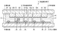
図1ないし図5において、11は基板装置としての透過型でかつアクティブマトリクス型のマルチドメイン型VANモード(MVAモード)の表示素子である液晶表示素子、すなわち液晶セルを示し、この液晶セル11は、アレイ基板12と対向基板13とが対向配置されているとともに、これら基板12,13間に液晶分子である複数のダイレクタLCを備えた光変調層としての液晶層14が介在され、かつ、基板12,13間の距離すなわちギャップが、例えば樹脂により形成された間隙保持部材である複数のスペーサ15によって保持されている。さらに、アレイ基板12と対向基板13とは、液晶層14を構成する液晶材料を注入する図示しない液晶注入口を除く外周を囲むように配置される接着部であるシール部17によって接着されている。そして、液晶セル11には、アレイ基板12と対向基板13とに、偏光板18,19が貼り付けられている。また、液晶セル11の背面側には、図示しない面光源であるバックライトが配置されている。
In FIG. 1 to FIG. 5, reference numeral 11 denotes a liquid crystal display element, that is, a liquid crystal cell, which is a transmissive and active matrix type multi-domain VAN mode (MVA mode) display element as a substrate device. The array substrate 12 and the counter substrate 13 are arranged to face each other, and a
アレイ基板12は、透光性および絶縁性を有するアレイ基板本体としての透明基板すなわちガラス基板21の液晶層14側の主面上に、例えばモリブデン(Mo)などにより形成された走査線22、この走査線22から突出したゲート電極23、および、図示しない補助容量線がパターン形成されているとともに、これら走査線22、ゲート電極23および補助容量線を覆って、例えば酸化シリコン膜などのゲート絶縁膜25が形成されている。また、このゲート絶縁膜25上には、ゲート電極23の位置に対応してノンドープアモルファスシリコン(a−Si)などの半導体層26およびリンドープアモルファスシリコンなどの低抵抗半導体層(コンタクト層)27が積層されているとともに、例えば窒化シリコン膜などのエッチング保護層29が形成されている。さらに、これら低抵抗半導体層27およびエッチング保護層29の一部を覆って、信号線31、この信号線31から突出したドレイン電極32、および、島状のソース電極33が形成されている。これらゲート電極23、半導体層26、低抵抗半導体層27、ドレイン電極32およびソース電極33などにより、スイッチング素子としての薄膜トランジスタ(TFT)35が形成されている。また、信号線31、ドレイン電極32およびソース電極33を覆って、窒化シリコン膜などの絶縁性の保護膜37が形成されているとともに、この保護膜37上の所定位置に、絶縁層としての有機膜38と、高誘電率絶縁層としての酸化チタン膜39が形成されている。そして、これら有機膜38と酸化チタン膜39とを覆って、例えばITO(Indium Tin Oxide)などの透明導電材料により、画素(副画素)41を構成する透明電極である画素電極42が形成されているとともに、走査線22と信号線31との交差位置に上記スペーサ15が配置されている。さらに、これらを覆って保護膜37上に配向膜44および重合性化合物層45が順次形成されている。
The array substrate 12 is a transparent substrate as a light-transmitting and insulating array substrate body, that is, a
走査線22および信号線31は、各画素41の間に格子状に形成されている。
The scanning lines 22 and the
各薄膜トランジスタ35は、ソース電極33が画素電極42と接続されており、走査線駆動回路であるゲートドライバ46からの信号が走査線22を介してゲート電極23に印加されることでスイッチング制御され、信号線駆動回路であるソースドライバ47から信号線31を介して入力された信号に対応して画素電極42に電圧を印加することで、画素41をそれぞれ独立して点灯/消灯制御するものである。
In each
各画素電極42は、平面視で例えば40μm×120μm程度の略長方形状に形成されており、各薄膜トランジスタ35と対応する位置が四角形状に切り欠き形成された切欠部42aとなっている。また、各画素電極42の切欠部42aの近傍には、各画素電極42を各薄膜トランジスタ35のソース電極33と電気的に接続するための図示しない凹状パターンであるコンタクトホールが形成されている。さらに、各画素電極42の左右両辺近傍には、図2中の左右方向すなわち画素電極42の幅方向に、液晶層14のダイレクタLCの倒れ方向を制御する長手状の欠落部としての電極スリット部42bが複数形成されている。
Each
各電極スリット部42bは、例えば幅寸法が5μm程度、長手寸法が20μm程度に形成され、それぞれ5μm程度のピッチで並んで形成されている。したがって、各画素電極42には、両辺に対応する電極スリット部42b間に、櫛歯状の対向突起42cが複数形成されている。
Each electrode slit
有機膜38は、可視光領域で透明に形成されている。また、この有機膜38は、比誘電率が例えばアレイ基板12のガラス基板21よりも高く設定されている。
The organic film 38 is formed transparent in the visible light region. The organic film 38 is set to have a relative dielectric constant higher than that of the
酸化チタン膜39は、有機膜38よりも比誘電率が高いもので、可視光領域で透明に形成されている。この酸化チタン膜39の比誘電率は、例えば10以上に設定されている。
The
重合性化合物層45は、例えばアクリル系の光硬化樹脂などにより形成され、可視光領域で透明に形成されている。
The
対向基板13は、透光性および絶縁性を有する対向基板本体としての透明基板すなわちガラス基板51の一主面上の、アレイ基板12側の薄膜トランジスタ35と対応する位置に、赤(R)、緑(G)および青(B)に対応する着色部52r,52g,52bを有する着色層としてのカラーフィルタ層52が例えばストライプ状にそれぞれ形成されている。また、このカラーフィルタ層52を覆って、例えばITO(Indium Tin Oxide)などの透明導電材料により形成された共通電極(透明電極)である対向電極53が形成されているとともに、カラーフィルタ層52の周囲に遮光部である額縁部54が形成されている。そして、対向電極53を覆って配向膜55および重合性化合物層56が形成されている。
The counter substrate 13 has a red (R), green color at a position corresponding to the
対向電極53は、各画素41に対応する位置に、スリット53aがそれぞれ形成されている。このスリット53aは、画素電極42の左右方向の略中心位置に沿って長手状に形成され、画素電極42の左右の電極スリット部42b,42b間に位置している。
In the
そして、これら電極スリット部42bおよびスリット53aにより、各画素41に対応する位置で液晶層14が複数、例えば2種類のドメインD1,D2に複数に分割されている。すなわち、これらドメインD1,D2は、各画素電極42の幅方向に隣接して形成されている。ここで、ドメインD1,D2内に位置する液晶層14の各ダイレクタLCは、電圧印加時の倒れ方向が、対向基板13側がそれぞれスリット53a側となるように傾斜している。また、各ダイレクタLCは、各電極スリット部42b内に位置するものが、これら電極スリット部42bの内辺に略平行な方向となっている。
The electrode slit
額縁部54は、遮光性を有する部材によりシール部17の内縁部に沿って枠状に形成されている。
The
重合性化合物層56は、重合性化合物層45と同様に、例えばアクリル系の光硬化樹脂などにより形成され、可視光領域で透明に形成されている。
Similarly to the
また、液晶層14は、所定の液晶材料により形成された光変調層であり、アレイ基板12側の重合性化合物45と、対向基板13側の重合性化合物層56との間に介在されている。この液晶層14は、負の誘電率異方性を有している。そして、ダイレクタLCは、配向膜44,55によりその配向方向が基板面と略垂直になるように制御されている。
The
また、スペーサ15は、例えば導電性を有さない透明樹脂などにより柱状に形成されている。
Further, the
また、液晶注入口は、シール部17によってその縁部が区画されており、例えば紫外線硬化樹脂などにより形成された図示しない封止材にて封止されている。
Further, the liquid crystal injection port has an edge portion defined by a
偏光板18,19は、一方の透過軸が図中の左右方向、他方の透過軸が図中の上下方向に沿うように配置されている。このため、偏光板18,19は、互いに透過軸が略直交するクロスニコル偏光板となっており、これら偏光板18,19の透過軸と液晶層14のダイレクタ38の光軸とが、略45°で交差するように構成されている。
The polarizing plates 18 and 19 are arranged so that one transmission axis is in the horizontal direction in the figure and the other transmission axis is in the vertical direction in the figure. Therefore, the polarizing plates 18 and 19 are crossed Nicol polarizing plates whose transmission axes are substantially orthogonal to each other, and the transmission axes of the polarizing plates 18 and 19 and the optical axis of the director 38 of the
次に、上記第1の実施の形態の液晶表示素子の製造方法を説明する。 Next, a method for manufacturing the liquid crystal display element of the first embodiment will be described.
液晶セル11は、ここでは一般的なプロセスを用いた成膜とパターニングとの繰り返しにより作製する。 Here, the liquid crystal cell 11 is manufactured by repeating film formation and patterning using a general process.
すなわち、まず、アレイ基板12のガラス基板21上に、例えばモリブデンなどの部材を例えば膜厚0.3μmでスパッタリングなどにより成膜し(第1成膜工程)、フォトリソグラフィなどにより走査線22(ゲート電極23)および補助容量線を所定の形状にパターン形成する(パターン形成工程)。
That is, first, a member such as molybdenum is formed on the
その上に、例えば膜厚0.15μmの酸化シリコンなどからなるゲート絶縁膜25、アモルファスシリコンなどの半導体層26、低抵抗半導体層27、および窒化シリコンなどからなるエッチング保護層29を形成する(第2成膜工程)。
A
その後、例えばアルミニウム(Al)を膜厚0.3μm程度でスパッタリング成膜し、フォトリソグラフィにより、信号線31(ドレイン電極32)、および、島状のソース電極33を同時に形成することで、薄膜トランジスタ35を形成する(薄膜トランジスタ(スイッチング素子)形成工程)。
Thereafter, for example, aluminum (Al) is formed by sputtering with a film thickness of about 0.3 μm, and the signal line 31 (drain electrode 32) and the island-shaped
さらに、薄膜トランジスタ35の上層に、窒化シリコンなどからなる絶縁性の保護膜37を形成する(保護膜形成工程)とともに、この保護膜37上に、絶縁性の有機膜38を例えば膜厚3.0μmで形成し、その上部に例えば膜厚0.2μmの酸化チタン膜39を成膜する(高誘電率絶縁膜形成工程)。
Further, an insulating
その後、例えばITOを膜厚0.1μm程度でスパッタリングして画素電極42を形成した(画素電極形成工程)後、フォトリソグラフィにより、この画素電極42に、例えば幅寸法5μm、長手寸法20μmの電極スリット部42bを5μmピッチで形成し(アレイ基板側スリット形成工程)、走査線22と信号線31との交差位置に、例えば高さ寸法が4.0μmの感光性樹脂材料からなるスペーサ15を形成する(スペーサ形成工程)。
Thereafter, for example, ITO is sputtered to a film thickness of about 0.1 μm to form the pixel electrode 42 (pixel electrode forming step), and then by photolithography, an electrode slit having a width dimension of 5 μm and a longitudinal dimension of 20 μm is formed on the
一方、対向基板13のガラス基板51上には、赤色の顔料を分散させた感光性レジストを塗布し、フォトリソグラフィにより赤色の着色部52rを形成した。同様にして、緑色の着色部52g、および、青色の着色部52bを形成することで、例えば膜厚1.0μm程度のカラーフィルタ層52を形成する(カラーフィルタ層(着色層)形成工程)。
On the other hand, a photosensitive resist in which a red pigment was dispersed was applied on the glass substrate 51 of the counter substrate 13, and a red
その後、例えばITOを膜厚約0.1μmでスパッタリングして対向電極53を形成した(対向電極形成工程)後、フォトリソグラフィにより、アレイ基板12上の電極スリット部42bと略直交する方向に沿って例えば幅10μmのスリット53aを作成する(対向基板側スリット形成工程)とともに、黒色樹脂レジストにより額縁部54を形成する(額縁部形成工程)。
Thereafter, for example, ITO is sputtered to a film thickness of about 0.1 μm to form the counter electrode 53 (counter electrode forming step), and then along the direction substantially orthogonal to the
さらに、アレイ基板12と対向基板13に、配向膜44,55を例えば70nmの厚さで塗布する(配向膜塗布工程)とともに、重合性化合物層45,56を所定の厚みで形成する(重合性化合物層形成工程)。
Further, the
その後、例えばエポキシ系の熱硬化樹脂からなる接着剤を用いたシール部17により、アレイ基板12と対向基板13とを所定の位置で貼り合わせ(貼り合わせ工程)、続いて、誘電率異方性が負の液晶材料を中空な液晶セル11に充填して液晶セル11を形成し、図示しない液晶注入口を紫外線硬化樹脂で封止する(注入口封止工程)。液晶層14のダイレクタLCは、配向膜44,55および重合性化合物層45,56により、ガラス基板21,51の基板面に対して略垂直な方向に配向制御される。
Then, for example, the array substrate 12 and the counter substrate 13 are bonded together at a predetermined position by the
そして、液晶セル11のガラス基板21,51に偏光板18,19を貼り付け(偏光板貼り付け工程)、液晶セル11を完成する。
Then, the polarizing plates 18 and 19 are attached to the
次に、上記第1の実施の形態の作用を説明する。 Next, the operation of the first embodiment will be described.
画素電極42と対向電極53との間に電圧を印加した際には、電界離散効果により、電界が電極スリット部42bの内側へと傾斜することで、ダイレクタLCが電極スリット部42bの外側(ダイレクタLCの電極スリット部42bから遠い部分が電極スリット部42bから離れる方向)へと傾斜する。
When a voltage is applied between the
このとき、電極スリット部42bから露出した高比誘電率(例えば20)の酸化チタン膜39により、電気力線の分布が、想像線L1に示す比誘電率7の状態に対して、画素電極42の各対向突起42cと電極スリット部42bとの縁部に沿うように交互に山状、谷状となる実線L2に示す状態となり、ダイレクタLCがこの電気力線の分布に沿って実線に示すように、電極スリット部42bの内縁に対して略平行に、すなわち偏光板18,19の透過軸に対して45°傾斜した状態に近づくように倒れる。
At this time, due to the
このように、上記第1の実施の形態によれば、液晶層14を複数のドメインD1,D2に分割するためのスリット53aと交差する方向に沿って画素電極42に電極スリット部42bを形成し、これら電極スリット部42bに対応する位置に形成した有機膜38よりも比誘電率が高い酸化チタン膜39を、電極スリット部42bを介して液晶層14側に露出するように形成することで、酸化チタン膜39によって各ドメインD1,D2の電界を設定して電極スリット部42b近傍のダイレクタLCと偏光板18,19の透過軸とのなす角度を45°に近づけ、ダイレクタLCの倒れ方向に起因する透過率の低下を抑制できる。
As described above, according to the first embodiment, the
すなわち、上記式(1)に示すように、偏光板18,19の透過軸とダイレクタLCとのなす角度が45°となるときに、透過率が最大となる。一方で、電極スリット部42bの幅寸法は透過率改善のために小さい方が好ましいものの、このように電極スリット部42bの幅寸法を小さくした場合には、電界離散効果が変化し、偏光板18,19の透過軸とダイレクタLCとのなす角度が45°からずれるおそれがある。このため、上記第1の実施の形態では、電極スリット部42bに酸化チタン膜39を配置することで、電極スリット部42bでの電界を変化させ、偏光板18,19の透過軸とダイレクタLCとのなす角度を45°に近づけることで、高コントラスト比および広視角範囲を得ることができるMVAモードの液晶セル11において、電極スリット部42bの幅寸法を小さくしつつ大きな透過率を得ることができる。
That is, as shown in the above formula (1), the transmittance is maximized when the angle formed between the transmission axes of the polarizing plates 18 and 19 and the director LC is 45 °. On the other hand, although the width dimension of the
また、酸化チタン膜39が10以上の比誘電率を有することで、透過率およびコントラストの低下を、より確実に抑制できる。
Further, since the
さらに、高誘電率絶縁層として酸化チタン膜39を用いることで、製造性および加工性などを確保し、コストを抑制できる。
Furthermore, by using the
そして、配向膜44,55と液晶層14との間に重合性化合物層45,56を形成することで、ダイレクタLCの倒れ方向を、より確実に制御でき、高透過率および高コントラストを得ることができる。
Further, by forming the polymerizable compound layers 45 and 56 between the
なお、上記第1の実施の形態において、図6に示す第2の実施の形態のように、有機膜38を形成しない場合でも、酸化チタン膜39の比誘電率をガラス基板21の比誘電率よりも高く設定することにより、電気力線の分布が変わり、上記第1の実施の形態と同様の作用効果を奏することが可能になる。
In the first embodiment, the relative dielectric constant of the
また、スリットは、対向電極53側に形成してもよい。
Further, the slit may be formed on the
さらに、高誘電率絶縁層としては、酸化チタン膜39に限らず、酸化チタンを一部に含むもの、あるいは、他の様々な膜などを用いることができる。
Further, the high dielectric constant insulating layer is not limited to the
そして、上記第1の実施の形態に対応する実施例1、および、上記第1の実施の形態の一部を変更した実施例2と、従来例に対応する比較例1ないし3とについての特性評価の結果を図7に示す。 Characteristics of Example 1 corresponding to the first embodiment, Example 2 in which a part of the first embodiment is changed, and Comparative Examples 1 to 3 corresponding to the conventional example The result of evaluation is shown in FIG.
実施例2の液晶セルは、電極スリット部42bの幅寸法およびピッチ(対向突起42cの幅寸法)をそれぞれ10μmとした。
In the liquid crystal cell of Example 2, the width dimension and pitch of the electrode slit
比較例1の液晶セルは、酸化チタン膜39を形成しない以外は、上記実施例1と同様の設計およびプロセスで作製した。
The liquid crystal cell of Comparative Example 1 was produced by the same design and process as Example 1 except that the
比較例2の液晶セルは、酸化チタン膜39を形成しない以外は、上記実施例2と同様の設計およびプロセスで作製した。
The liquid crystal cell of Comparative Example 2 was produced by the same design and process as in Example 2 except that the
比較例3の液晶セルは、高誘電率絶縁層として、比誘電率が7のものを使用する以外は、実施例1と同様の設計およびプロセスで作製した。 The liquid crystal cell of Comparative Example 3 was produced by the same design and process as Example 1 except that a high dielectric constant insulating layer having a relative dielectric constant of 7 was used.
図7に示すように、実施例1と実施例2との比較により、電極スリット部42bの幅寸法は、小さい方が透過率およびコントラストの面で好ましいことが示された。
As shown in FIG. 7, the comparison between Example 1 and Example 2 shows that the smaller width dimension of the
また、実施例1および実施例2に対して、比較例1および比較例2はそれぞれ透過率およびコントラストが低下している。このため、酸化チタン膜39を電極スリット部42bから露出するように形成することの有効性が示された。
In contrast to Example 1 and Example 2, Comparative Example 1 and Comparative Example 2 have lower transmittance and contrast, respectively. Therefore, the effectiveness of forming the
さらに、実施例1に対して、比較例3は透過率およびコントラストが低下している。このため、高誘電率絶縁層として用いる酸化チタン膜39の比誘電率は7よりも大きい方が好ましいことが示された。
Furthermore, the transmittance and contrast of Comparative Example 3 are lower than Example 1. For this reason, it was shown that the relative dielectric constant of the
11 液晶表示素子としての液晶セル
12 アレイ基板
13 対向基板
14 液晶層
18,19 偏光板
21 アレイ基板本体としてのガラス基板
38 絶縁層としての有機膜
39 高誘電率絶縁層としての酸化チタン膜
42 画素電極
42b 欠落部としての電極スリット部
44,55 配向膜
45,56 重合性化合物層
51 対向基板本体としてのガラス基板
53 対向電極
53a スリット
D1,D2 ドメイン
LC 液晶分子であるダイレクタ
11 Liquid crystal cells as liquid crystal display elements
12 Array substrate
13 Counter substrate
14 Liquid crystal layer
18, 19 Polarizer
21 Glass substrate as the main body of the array substrate
38 Organic film as an insulating layer
39 Titanium oxide film as high dielectric constant insulating layer
42 Pixel electrode
42b Electrode slit as missing part
44, 55 Alignment film
45, 56 Polymerizable compound layer
51 Glass substrate as counter substrate body
53 Counter electrode
53a slit
D1, D2 domain
Director of LC liquid crystal molecules
Claims (5)
対向基板本体およびこの対向基板本体の主面側に形成された対向電極を備え、前記アレイ基板に対向配置された対向基板と、
誘電率異方性が負の液晶材料を備え、前記アレイ基板と前記対向基板との間に介在された液晶層と、
前記アレイ基板と前記対向基板とのそれぞれに配置され、互いの透過軸が略直交する偏光板と、
前記対向電極に形成され、前記液晶層を前記画素電極と前記対向電極との間の電圧印加時の液晶分子の倒れ方向が互いに異なる複数のドメインに分割するためのスリットと、
このスリットと交差する方向に沿って前記画素電極に設けられ、前記各ドメイン内の前記液晶分子の倒れ方向を制御する欠落部と、
前記欠落部を介して前記液晶層側に露出し、可視光領域で透明でかつ前記アレイ基板本体よりも比誘電率が高い高誘電率絶縁層と
を具備したことを特徴とする液晶表示素子。 An array substrate having an array substrate body and a plurality of pixel electrodes formed on the main surface side of the array substrate body;
A counter substrate provided with a counter substrate body and a counter electrode formed on the main surface side of the counter substrate body, and disposed opposite to the array substrate;
A liquid crystal layer having a negative dielectric anisotropy, and a liquid crystal layer interposed between the array substrate and the counter substrate;
A polarizing plate that is disposed on each of the array substrate and the counter substrate, and whose transmission axes are substantially orthogonal to each other,
A slit formed on the counter electrode for dividing the liquid crystal layer into a plurality of domains having different tilt directions of liquid crystal molecules when a voltage is applied between the pixel electrode and the counter electrode;
Provided on the pixel electrodes along a direction intersecting with the slit, a missing portion that controls the falling direction of the liquid crystal molecules in said each domain,
Liquid crystal display, characterized in that said missing portion is exposed to the liquid crystal layer side through a and transparent in the visible light region and the array substrate Body by Rimohi dielectric constant; and a high high-k insulating layer element.
対向基板本体およびこの対向基板本体の主面側に形成された対向電極を備え、前記アレイ基板に対向配置された対向基板と、
誘電率異方性が負の液晶材料を備え、前記アレイ基板と前記対向基板との間に介在された液晶層と、
前記アレイ基板と前記対向基板とのそれぞれに配置され、互いの透過軸が略直交する偏光板と、
前記対向電極に形成され、前記液晶層を前記画素電極と前記対向電極との間の電圧印加時の液晶分子の倒れ方向が互いに異なる複数のドメインに分割するためのスリットと、
このスリットと交差する方向に沿って前記画素電極に設けられ、前記各ドメイン内の前記液晶分子の倒れ方向を制御する欠落部と、
少なくとも前記欠落部に対応する位置に形成され、可視光領域で透明な絶縁層と、
この絶縁層を少なくとも前記欠落部に対応する位置で覆ってこの欠落部を介して前記液晶層側に露出し、可視光領域で透明でかつ前記絶縁層よりも比誘電率が高い高誘電率絶縁層と
を具備したことを特徴とする液晶表示素子。 An array substrate having an array substrate body and a plurality of pixel electrodes formed on the main surface side of the array substrate body;
A counter substrate provided with a counter substrate body and a counter electrode formed on the main surface side of the counter substrate body, and disposed opposite to the array substrate;
A liquid crystal layer having a negative dielectric anisotropy, and a liquid crystal layer interposed between the array substrate and the counter substrate;
A polarizing plate that is disposed on each of the array substrate and the counter substrate, and whose transmission axes are substantially orthogonal to each other,
A slit formed on the counter electrode for dividing the liquid crystal layer into a plurality of domains having different tilt directions of liquid crystal molecules when a voltage is applied between the pixel electrode and the counter electrode;
Provided on the pixel electrodes along a direction intersecting with the slit, a missing portion that controls the falling direction of the liquid crystal molecules in said each domain,
An insulating layer that is formed at least in a position corresponding to the missing portion and is transparent in the visible light region;
The insulating layer is covered at least at a position corresponding to the missing portion, exposed to the liquid crystal layer side through the missing portion, is transparent in the visible light region, and has a high dielectric constant insulation having a higher relative dielectric constant than the insulating layer. A liquid crystal display element comprising: a layer.
ことを特徴とする請求項1または2記載の液晶表示素子。 The liquid crystal display element according to claim 1, wherein the high dielectric constant insulating layer has a relative dielectric constant of 10 or more.
ことを特徴とする請求項3記載の液晶表示素子。 The liquid crystal display element according to claim 3, wherein the high dielectric constant insulating layer contains titanium oxide.
これら配向膜と前記液晶層との間に形成された重合性化合物層と
を具備したことを特徴とする請求項4記載の液晶表示素子。 Alignment films respectively formed on the liquid crystal layer side of the array substrate and the counter substrate;
The liquid crystal display element according to claim 4, further comprising: a polymerizable compound layer formed between the alignment film and the liquid crystal layer.
Priority Applications (2)
| Application Number | Priority Date | Filing Date | Title |
|---|---|---|---|
| JP2008100196A JP4636626B2 (en) | 2008-04-08 | 2008-04-08 | Liquid crystal display element |
| US12/349,315 US8018561B2 (en) | 2008-04-08 | 2009-01-06 | Liquid crystal display element |
Applications Claiming Priority (1)
| Application Number | Priority Date | Filing Date | Title |
|---|---|---|---|
| JP2008100196A JP4636626B2 (en) | 2008-04-08 | 2008-04-08 | Liquid crystal display element |
Publications (2)
| Publication Number | Publication Date |
|---|---|
| JP2009251346A JP2009251346A (en) | 2009-10-29 |
| JP4636626B2 true JP4636626B2 (en) | 2011-02-23 |
Family
ID=41132938
Family Applications (1)
| Application Number | Title | Priority Date | Filing Date |
|---|---|---|---|
| JP2008100196A Active JP4636626B2 (en) | 2008-04-08 | 2008-04-08 | Liquid crystal display element |
Country Status (2)
| Country | Link |
|---|---|
| US (1) | US8018561B2 (en) |
| JP (1) | JP4636626B2 (en) |
Families Citing this family (2)
| Publication number | Priority date | Publication date | Assignee | Title |
|---|---|---|---|---|
| JP5514418B2 (en) * | 2008-09-05 | 2014-06-04 | 株式会社ジャパンディスプレイ | Liquid crystal display |
| TWI490596B (en) * | 2012-09-14 | 2015-07-01 | Innocom Tech Shenzhen Co Ltd | Display device |
Citations (3)
| Publication number | Priority date | Publication date | Assignee | Title |
|---|---|---|---|---|
| JP2001249350A (en) * | 2000-03-03 | 2001-09-14 | Nec Corp | Liquid crystal display device and method of manufacturing the same |
| JP2003186017A (en) * | 2001-10-12 | 2003-07-03 | Fujitsu Display Technologies Corp | Liquid crystal display device |
| JP2003322869A (en) * | 2002-05-06 | 2003-11-14 | Oobayashi Seiko Kk | Liquid crystal display of ultra-high aperture ratio and wide visual field angle |
Family Cites Families (2)
| Publication number | Priority date | Publication date | Assignee | Title |
|---|---|---|---|---|
| KR100628263B1 (en) * | 2002-08-21 | 2006-09-27 | 엘지.필립스 엘시디 주식회사 | Liquid crystal display device |
| JP2005292515A (en) | 2004-03-31 | 2005-10-20 | Sharp Corp | Liquid crystal display device and its driving method, and electronic equipment |
-
2008
- 2008-04-08 JP JP2008100196A patent/JP4636626B2/en active Active
-
2009
- 2009-01-06 US US12/349,315 patent/US8018561B2/en active Active
Patent Citations (3)
| Publication number | Priority date | Publication date | Assignee | Title |
|---|---|---|---|---|
| JP2001249350A (en) * | 2000-03-03 | 2001-09-14 | Nec Corp | Liquid crystal display device and method of manufacturing the same |
| JP2003186017A (en) * | 2001-10-12 | 2003-07-03 | Fujitsu Display Technologies Corp | Liquid crystal display device |
| JP2003322869A (en) * | 2002-05-06 | 2003-11-14 | Oobayashi Seiko Kk | Liquid crystal display of ultra-high aperture ratio and wide visual field angle |
Also Published As
| Publication number | Publication date |
|---|---|
| US8018561B2 (en) | 2011-09-13 |
| JP2009251346A (en) | 2009-10-29 |
| US20090251651A1 (en) | 2009-10-08 |
Similar Documents
| Publication | Publication Date | Title |
|---|---|---|
| JP4248835B2 (en) | Substrate for liquid crystal display device and liquid crystal display device including the same | |
| JP4543006B2 (en) | Liquid crystal display element and manufacturing method thereof | |
| US9341898B2 (en) | Liquid crystal display device | |
| JP2002182230A (en) | Fringe field switching mode liquid crystal display | |
| JP5127485B2 (en) | Liquid crystal display | |
| CN108957873B (en) | Liquid crystal display device having a plurality of pixel electrodes | |
| US20070040974A1 (en) | Liquid crystal display panel | |
| KR20040062146A (en) | Liquid crystal display panel and fabricating method thereof | |
| US8081274B2 (en) | Liquid crystal device having a first polarizing element deviated up to a range of plus or minus 1 degree relative to a Y axis of a second polarizing element | |
| JP4334412B2 (en) | Liquid crystal display | |
| US20070165166A1 (en) | Liquid crystal display device | |
| JP2009186822A (en) | Liquid crystal display panel and manufacturing method of liquid crystal display panel | |
| JP4636626B2 (en) | Liquid crystal display element | |
| WO2016031638A1 (en) | Liquid-crystal display | |
| JP2004245952A (en) | Liquid crystal display device | |
| JP5677923B2 (en) | Liquid crystal display | |
| US8384866B2 (en) | Liquid crystal display device comprising first and second organic alignment films having slow axes arranged to cross each other by aligning polymer chains | |
| JP3631179B2 (en) | Liquid crystal display | |
| JP2004219827A (en) | Liquid crystal display | |
| WO2013122184A1 (en) | Liquid crystal display manufacturing method | |
| JP2009031437A (en) | Liquid crystal display panel | |
| JP2002090751A (en) | Liquid crystal display device and method for manufacturing the same | |
| JP2007121642A (en) | Liquid crystal display device | |
| JP2007133054A (en) | Liquid crystal display device | |
| JP2007139859A (en) | Liquid crystal display device |
Legal Events
| Date | Code | Title | Description |
|---|---|---|---|
| A621 | Written request for application examination |
Free format text: JAPANESE INTERMEDIATE CODE: A621 Effective date: 20100326 |
|
| A977 | Report on retrieval |
Free format text: JAPANESE INTERMEDIATE CODE: A971007 Effective date: 20100802 |
|
| A131 | Notification of reasons for refusal |
Free format text: JAPANESE INTERMEDIATE CODE: A131 Effective date: 20100818 |
|
| A521 | Request for written amendment filed |
Free format text: JAPANESE INTERMEDIATE CODE: A523 Effective date: 20100916 |
|
| TRDD | Decision of grant or rejection written | ||
| A01 | Written decision to grant a patent or to grant a registration (utility model) |
Free format text: JAPANESE INTERMEDIATE CODE: A01 Effective date: 20101027 |
|
| A01 | Written decision to grant a patent or to grant a registration (utility model) |
Free format text: JAPANESE INTERMEDIATE CODE: A01 |
|
| A61 | First payment of annual fees (during grant procedure) |
Free format text: JAPANESE INTERMEDIATE CODE: A61 Effective date: 20101119 |
|
| FPAY | Renewal fee payment (event date is renewal date of database) |
Free format text: PAYMENT UNTIL: 20131203 Year of fee payment: 3 |
|
| R150 | Certificate of patent or registration of utility model |
Ref document number: 4636626 Country of ref document: JP Free format text: JAPANESE INTERMEDIATE CODE: R150 Free format text: JAPANESE INTERMEDIATE CODE: R150 |
|
| S533 | Written request for registration of change of name |
Free format text: JAPANESE INTERMEDIATE CODE: R313533 |
|
| FPAY | Renewal fee payment (event date is renewal date of database) |
Free format text: PAYMENT UNTIL: 20131203 Year of fee payment: 3 |
|
| R350 | Written notification of registration of transfer |
Free format text: JAPANESE INTERMEDIATE CODE: R350 |
|
| R250 | Receipt of annual fees |
Free format text: JAPANESE INTERMEDIATE CODE: R250 |
|
| R250 | Receipt of annual fees |
Free format text: JAPANESE INTERMEDIATE CODE: R250 |
|
| R250 | Receipt of annual fees |
Free format text: JAPANESE INTERMEDIATE CODE: R250 |
|
| R250 | Receipt of annual fees |
Free format text: JAPANESE INTERMEDIATE CODE: R250 |
|
| R250 | Receipt of annual fees |
Free format text: JAPANESE INTERMEDIATE CODE: R250 |
|
| R250 | Receipt of annual fees |
Free format text: JAPANESE INTERMEDIATE CODE: R250 |
|
| R250 | Receipt of annual fees |
Free format text: JAPANESE INTERMEDIATE CODE: R250 |
|
| R250 | Receipt of annual fees |
Free format text: JAPANESE INTERMEDIATE CODE: R250 |
|
| S111 | Request for change of ownership or part of ownership |
Free format text: JAPANESE INTERMEDIATE CODE: R313111 |
|
| R350 | Written notification of registration of transfer |
Free format text: JAPANESE INTERMEDIATE CODE: R350 |
|
| R250 | Receipt of annual fees |
Free format text: JAPANESE INTERMEDIATE CODE: R250 |
|
| R250 | Receipt of annual fees |
Free format text: JAPANESE INTERMEDIATE CODE: R250 |
|
| R250 | Receipt of annual fees |
Free format text: JAPANESE INTERMEDIATE CODE: R250 |