JP4635213B2 - Zero delay mask for Galois LFSR - Google Patents
Zero delay mask for Galois LFSR Download PDFInfo
- Publication number
- JP4635213B2 JP4635213B2 JP2001548538A JP2001548538A JP4635213B2 JP 4635213 B2 JP4635213 B2 JP 4635213B2 JP 2001548538 A JP2001548538 A JP 2001548538A JP 2001548538 A JP2001548538 A JP 2001548538A JP 4635213 B2 JP4635213 B2 JP 4635213B2
- Authority
- JP
- Japan
- Prior art keywords
- output
- input
- register
- value
- series
- Prior art date
- Legal status (The legal status is an assumption and is not a legal conclusion. Google has not performed a legal analysis and makes no representation as to the accuracy of the status listed.)
- Expired - Fee Related
Links
Images

Classifications
-
- H—ELECTRICITY
- H04—ELECTRIC COMMUNICATION TECHNIQUE
- H04J—MULTIPLEX COMMUNICATION
- H04J13/00—Code division multiplex systems
- H04J13/10—Code generation
-
- H—ELECTRICITY
- H04—ELECTRIC COMMUNICATION TECHNIQUE
- H04B—TRANSMISSION
- H04B1/00—Details of transmission systems, not covered by a single one of groups H04B3/00 - H04B13/00; Details of transmission systems not characterised by the medium used for transmission
- H04B1/69—Spread spectrum techniques
- H04B1/707—Spread spectrum techniques using direct sequence modulation
-
- G—PHYSICS
- G06—COMPUTING; CALCULATING OR COUNTING
- G06F—ELECTRIC DIGITAL DATA PROCESSING
- G06F7/00—Methods or arrangements for processing data by operating upon the order or content of the data handled
- G06F7/58—Random or pseudo-random number generators
- G06F7/582—Pseudo-random number generators
- G06F7/584—Pseudo-random number generators using finite field arithmetic, e.g. using a linear feedback shift register
-
- H—ELECTRICITY
- H04—ELECTRIC COMMUNICATION TECHNIQUE
- H04J—MULTIPLEX COMMUNICATION
- H04J13/00—Code division multiplex systems
- H04J13/0007—Code type
- H04J13/0022—PN, e.g. Kronecker
Landscapes
- Engineering & Computer Science (AREA)
- Computer Networks & Wireless Communication (AREA)
- Signal Processing (AREA)
- Physics & Mathematics (AREA)
- Theoretical Computer Science (AREA)
- General Physics & Mathematics (AREA)
- Mathematical Analysis (AREA)
- Mathematical Optimization (AREA)
- Pure & Applied Mathematics (AREA)
- General Engineering & Computer Science (AREA)
- Computational Mathematics (AREA)
- Error Detection And Correction (AREA)
- Manipulation Of Pulses (AREA)
Description
【0001】
【発明の属する技術分野】
この発明は、データを符号化したり復号化したりするための疑似雑音シーケンスを用いる、例えばCDMA−2000、UMTS、IS−95標準やこれと同様のセルラ電話システムなどを実現するための、直接シーケンススペクトラム拡散通信システムに関する。
【0002】
【発明の背景】
スペクトラム拡散通信システムは、増加された用途と、双方向の空中の通信とを見出している。丁度AMおよびFMシステムが情報を運ぶために正弦波信号を用いているように、スペクトラム拡散システムは、情報を運ぶために雑音のような信号を用いている。送信機においては、デジタルデータストリームが、媒体を介してデータを送信するために、疑似雑音シーケンス(PNS)を用いて信号のスペクトルを拡散するために符号化される。受信機では、データが媒体から復元されて、その後、同じPNSを用いて信号のスペクトルを逆拡散し、最初のデジタルデータストリームを再生するために復号化されている。
【0003】
PNSは、有限のパターンを伴うビットのストリームであるが、これはランダムなビットストリームであるように見える。PNSを生成する共通の装置は線形フィードバックシフトレジスタ(LFSR-linear feedback shift register-)である。LFSRの2つの普通のタイプは、フィボナッチ(Fibonacci)LFSRとガロア(Galois)LFSRである。両方のタイプとも、ループを介してビットがシフトされるビットレジスタとモジュロ2加算器を含む閉鎖されたループ回路を含んでいる。加算器はループの一部分である1つの入力と、ループの他の部分に接続された他の入力とを有し、それらがループを介してシフトされるように、ビットをランダム化するための複数のループを形成している。
【0004】
何れかのLFSR用のPNSの値は、大きな数のビットの後に繰り返されると共に、制限された量のハードウェアを使用することを繰り返すことなく、最長可能シーケンスを有するPNSを提供することが望まれている。これは、LFSRの加算器とレジスタとの構成と、この技術分野で公知の方法でのレジスタの初期値とを選択することにより実現されている。LFSRに含まれているm個のレジスタの所定の数のために、PNSの最長可能非反復部分は、2m−1ビットまでの長さに等しくなる。
【0005】
同じPNSを用いることに加えて、送信機と受信機はそれぞれ拡散および逆拡散するためのPNS内の同じ位置からの値を用いなければならない。PSN内の同一の位置での値を両者が用いるため送信機と受信機を同期させるために、オフセットマスク値が計算されて、この技術分野で公知の方法によりPNS内の異なるシフトされた位置の値を生成するために(送信機または受信機内の)PNSの連続する位置の出力値と前記オフセットマスク値とが結合されている。
【0006】
この技術分野の熟練者たちは、以下の引用例に向けられている。シーデンバーグ(Siedenburg)に付与された合衆国特許第5,878,076号は、直接シーケンススペクトラム拡散通信システムを説明している。トーマス(Thomas)に付与された合衆国特許第5,754,603号は、PNSの同期について説明している。バロン(Barron)に付与された合衆国特許第5,926,070号は、オフセットマスクの生成を説明している。石田(Ishida)によるヨーロッパ特許出願第0660541号は、送信機と受信機のPNS位置を同期させる方法を説明している。メドロック(Medlock)によるPCT特許出願の国際公開WO99/45670号は、LFSR用のマスクを説明している。
【0007】
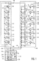
図1は、オフセットマスクを有するガロアLFSRの選択された部分を説明している。LFSR100は、ループ回路内で直列に接続された多数のバイナリレジスタ101−108を備えている。バイナリレジスタは、D型フリップフロップでも、または他の公知のビットレジスタ装置でも良い。一例として、レジスタ102を用いると、各々のレジスタ102は前段のレジスタ101の出力111に接続された値を持つ入力110を有し、各々のレジスタ102は後段のレジスタ103の値のある入力113に接続された出力112を有している。
【0008】
LFSR100はまた、ループ回路内で接続された1つまたはそれ以上のモジュロ2加算器115−117を含んでいる。各々の加算器は、レジスタ列の異なるペアの連続するレジスタ101−108の間に挿入されている。加算器がその間に挿入されたレジスタのペアの選択は原始多項式の選択により決まっている。原始多項式は、素数の概念と同様のものである。原始多項式は、何れかのより簡単な多項式により分割されることができる多項式である。図1に示されたLFSRの特別な例では、原始2値多項式は、D8+D4+D3+D2+1である。このD8は、LFSRに対して8つのレジスタを有することを要求しており、D2,D3およびD4の項は、図示されているように、レジスタのペアにおける最後から2番目のペアの間、最後から3番目のペアの間および最後から4番目のペアの間にそれぞれ挿入された加算器を要求している。素数のような原始多項式は、この技術分野においては良く知られている。
【0009】
挿入された加算器115−117はそれぞれ、2つの入力と1つの出力を有しており、XOR(排他的論理和)ゲートとして簡単に実施されていても良い。一例として、加算器115は、前段のレジスタ104の出力121に接続された第1の入力120と、後段のレジスタ105の値を持つ入力123に接続された出力122を有している。さらに、加算器115は、最終段のレジスタ108の出力125と、連続するレジスタの最初のレジスタ101の入力126との間に接続された第2の入力124を有している。クロック信号線130は、連続するレジスタのうちの各々のレジスタのクロック入力に接続されており、クロック信号がこのクロック信号線を介して送信されたときに、各レジスタは、そのときにそれレジスタの値を持つ入力で受信されている値を出力し始める。例えばクロック信号線130は、レジスタ101のクロック入力131に接続されている。
【0010】
制御線135は、レジスタの値を初期化するためにレジスタ101−108のそれぞれに接続された、少なくとも1つの初期化線136を含んでいる。例えば初期化線136は、レジスタ108の初期化入力137に接続されるように示されている。この初期化線は、レジスタにメモり値を書き込むようにしても良いので、何れかの初期値を所望の何れかのレジスタに書き込むことができる。もう1つの方法として、制御線は、個々のレジスタのハードウェア内に設定された幾つかの所定の初期値を仮定するために、レジスタに簡単に信号を送るようにしても良い。もしもこのレジスタがD型フリップフロップであるならば、初期化線は、“1(one)”に初期化されるべき全てのレジスタのセット入力に接続されると共に、“0(zero)”に初期化されるべき全てのレジスタのリセット入力に接続されており、初期化線がハイになるときに、レジスタの値はそれらの個別の初期値であると仮定している。個別の原始多項式のためのレジスタの初期値を選択する方法は公知のものであり、更なる議論はここでは求められていない。
【0011】
図1に示されたガロアLFSRは、PNSに関するビット値を出力138から出力している。しかしながら、受信機にPNSににおける出力値の位置を同一のPNSを用いる送信機のための出力値の位置に同期させる(その逆の場合もまた同様である)ために、オフセットマスク値がPNSの以前に出力されていた箇所に結合させられるべきである。
【0012】
マスク140は、図1に示されたようなガロアLFSR100の出力138に接続されている。このマスクは、LFSRからのPNS出力の前段の8ビットをそれぞれ記憶する一連のレジスタ141−148を含んでいる。レジスタ142−148の出力は、それぞれのレジスタに続くレジスタ141−147の入力に接続されている。例えば、レジスタ146の入力149は、レジスタ147の出力150に接続されており、レジスタ146の出力151は、レジスタ145の入力152に接続されている。
【0013】
マスクはさらに、一連のモジュロ2加算器161−167を含んでおり、連続する加算器162−167のそれぞれの第1の入力は加算器シリーズの個々の前段の加算器161−166のそれぞれの出力に接続されている。例えば、加算器165の入力153は、加算器164の出力154に接続されており、この加算器165の出力155は、加算器166の入力156に接続されている。多くのマスクスイッチ171−178は、前記加算器シリーズの第1の加算器161の第1の入力180に接続された出力179を有する第1のマスクスイッチ171を含んでいる。さらに、それに続くマスクスイッチ172−178は、前記加算器シリーズにおける加算器161−167のそれぞれの第2の入力に接続された出力を有している。それぞれのレジスタ141−148の出力は、個々のスイッチ171−178の入力にそれぞれ接続されている。
【0014】
制御線135のマスク値線191−198は、スイッチ171−178にそれぞれ接続されており、これは、個々のレジスタの値が個々のスイッチを介して加算器161−167の個々の加算器の入力へと供給されているか否かを制御する開放されたまたは閉鎖された位置に個々のスイッチ171−178をそれぞれセットするために接続されているものである。例えば、レジスタ146の出力151は、スイッチ175の入力182に接続されており、このスイッチ175の出力183は、加算器165の入力184に接続されている。したがって、スイッチ線196が“1”に設定されたときに、レジスタ146の値はその後、加算器164の出力154の出力値に加算されてモジュロ2となると共に、その結果は出力155から加算器166の入力156へと出力される。そうでなければ、スイッチ線183が“0”に設定されたときに、加算器164の出力154からの値はその後、加算器165を単純に通過して加算器166の入力156に供給されている。最後に、加算器シリーズの最終段のモジュロ2加算器167の出力に接続されている出力端子199は、マスクされたPNSの値を出力している。
【0015】
マイクロコントローラ200は、プロセッサ201と、クロック202と、メモリ203とを含んでおり、これらはバス204により相互接続されている。電力供給源205は、プロセッサ、メモリおよびクロックを動作させるための電力を提供している。クロックは、動作を同期させるためにプロセッサおよびメモリにタイミング信号を提供している。マイクロプロセッサのメモリは、レジスタ101−108用の初期値を含むデータモジュール206と、初期化の際にこれらのレジスタに対して制御線135を介してその初期値を送信してプロセッサを制御するためのプログラムモジュール207と、を含んでいる。このメモリはまた、この技術分野における公知のやり方により、マスク値を演算するプログラムモジュール208をも含んでいるので、送信機のマスクされたPNSにより提供される個々の値と受信機における対応する値とを同期させることができる。
【0016】
公知のマスクされたガロアLFSRにおいて、LFSRが初期化された後に、LFSRのマスクは、適正なPNSのビットがマスクの全てのレジスタの中に取り込まれるまで、無効なシーケンスを出力する。これは、送信機と受信機との間で同期をとっている間にLFSRを異なる初期値に初期化するようなシステムにおいては特に問題となる。
【0017】
上述した引用例は、これによりこの明細書の全体にわたって、参考として組み入れられるものとする。
【0018】
【発明の概要】
いくつかの応用を含むこの発明において、マスクされたガロア線形フィードバックシフトレジスタ(LFSR)は、このLFSRの初期化に直接基づいて、適正なマスクされた疑似雑音シーケンス(PNS)を出力することが可能である。これは、結合されたネットワークを介してガロアLFSRのマスクスイッチをLFSRのレジスタに相互接続することにより実現されている。この発明はまた、ガロアLFSRが実行する特定の原始多項式にもまた応じてLFSRのみにより決まるレジスタにスイッチをどのようにして相互接続するのかを決定するための単純な方法を提供している。
【0019】
この技術分野における熟練者たちは、請求の範囲の特徴を表現した以下に添付する図面を参照しながら、以下に説明される好適な実施形態の詳細な説明を詳しく調べることにより、この発明およびこの発明の付加的目的および長所を理解することになろう。
【0020】
【発明の実施の形態】
図においては、説明を簡略化するために、異なる図面に用いられた同一の構成要素は同一の符号を有するものとする。
【0021】
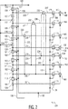
図2は、この発明に係るマスクされたガロア線形フィードバックシフトレジスタ(LFSR)220を示している。レジスタ101−108および加算器115−117を含むLFSRの構成要素および動作は、上述した図1のものと同様である。また、マスクにおいても、一連の加算器161−167およびこの一連加算器のそれぞれの加算器の各入力に接続されたスイッチ171−178は、本質的には図1に示されたものと同様である。
【0022】
図2のマスクされたLFSRにおいて、各ネットワークは、1つまたはそれ以上のレジスタ101−108の出力と、マスクスイッチ171−178の各々の入力と、の間に接続されている。このネットワークは、レジスタ125,101,102,103および104の出力と、各マスクスイッチ171,172,173,174および175の入力と、の間の1対1接続221,222,223,224および225を含んでいる。このネットワークは、レジスタ101および105の出力と、モジュロ2加算器231の入力との間の接続229および226と、モジュロ2加算器231の出力とマスクスイッチ176の入力との間の接続235と、を含んでいる。このネットワークは、レジスタ101,102および106の出力と、モジュロ2加算器232の入力との間の接続230,231および227と、モジュロ2加算器232の出力とマスクスイッチ177の入力との間の接続236と、を含んでいる。このネットワークはまた、レジスタ101,102,103および107の出力と、モジュロ2加算器233の入力との間の接続232,233,234および228と、モジュロ2加算器233の出力と、マスクスイッチ178の入力との間の接続237と、を含んでいる。
【0023】
レジスタおよびスイッチ間のネットワークの構成は、ガロアLFSRの構成より直接決定することができる。この場合、ガロアLFSRが第4,第5および第6のレジスタの出力に接続された加算器を有しているので、これにより接続は、レジスタの出力から第4,第5および第6のレジスタを越えてそれを行なうことができるスイッチへと延長すべきものである。接続229,231および234のみは、レジスタの出力から4つのレジスタを介してそれぞれのスイッチへと延長することができる。接続230および233のみは、5つのレジスタを介してそれぞれのスイッチへと延長することができる。接続232のみは、6つのレジスタを介してスイッチへと延長することができる。好ましくは、接続の数は、第1項を除いて、幾つかのより低い順番の項のみを有する原始多項式を選択することにより最小化される。すなわち、もしも多項式がD7項を有するならば、加算器はレジスタ101および102間に1つ挿入されるであろうし、接続はそれを行なうことができる1つのレジスタを介して延長されることになるであろうので加算器はスイッチ173,174および175のために求められるであろうし、さらに6つの接続が、レジスタ101,102,103,104,105および106からスイッチ173,174,175,176,177および178用の加算器にまでそれぞれ求められることになるであろう。
【0024】
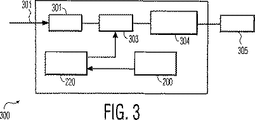
図3は、図2のマスクされたガロアLFSRを利用するこの発明の送信機300を示している。マイクロコントローラ200は、クロック,レジスタ初期化およびマスク信号をマスクされたガロアLFSR220に提供するために、図2に関連して上述したように、接続されている。情報信号は、入力301を介して符号化器302内に受信され、ここで情報を連続するビットストリームへと変換している。例えば、符号化器は、アナログ音声入力をビットストリームへと変換している。入力を介して受信された情報が既に連続するビットストリームであるならば、そのときは符号化器を必要としなくとも良い。拡散情報信号を提供するために、この発明に係るマスクされたガロアLFSR220のPNS出力に基づいて、拡散器303によりビットストリームが拡散される。送信機装置304は、拡散情報信号を媒体205内に送信する。送信機は、例えば、拡散情報信号を空中に放送するアンテナに接続された変調器;拡散情報信号をコンピュータ媒体に書き込むための媒体装置の書き込みヘッドに接続されたチャンネル符号化器;または光ファイバを介して送信するために接続されたレーザ装置またはその他の同等の情報送信システムであっても良い。
【0025】
図4は、図3の送信機により生成された拡散情報信号を受信し、送信機に最初に入力された情報信号を再生するための受信機320を示している。受信機装置321は、媒体305からの拡散情報信号を受信している。受信機の性質は、上述したように、媒体に基づいている。逆拡散器322は、上述したような符号化されたビットストリームを提供するために拡散情報を逆拡散している。復号化器323は、送信機300により最初に受信されていた情報信号を再生するために符号化されたビットストリームを復号化している。もしも符号化器が必要でなかったならば、状況によっては復号化器もまた必要でなくなるかもしれない。PNS発生器220は、図3のPNS発生器220と全く同じであり、好ましくは、図2のマスクされたガロアLFSR220である。PNS発生器220においては、疑似雑音シーケンス(PNS)の出力値は、PNSシーケンス内の異なる位置に対応する出力値を提供するために、この発明のマスクにより変形されてしまっているので、情報信号を拡散するため、および、拡散情報信号を逆拡散するために、同じ値を用いることができる。
【0026】
この発明は、この技術分野の熟練者たちにこの発明を想像し利用することを可能にするため、および、この発明を実施するために熟慮された最良の形態を説明するために、特別に好適な実施形態にしたがって説明されてきた。この技術分野の熟練者たちは、この発明の精神から逸脱することなく、これらの実施形態を変形したり、実施形態に付加したり、他の実施形態を提供したりしても良い。
【0027】
【発明の実施例】
出力手段が、レジスタ、D型フリップフロップ、およびワードメモリ:から選択されているメモリ内の処理された値を格納する、この発明の実施例によるシステム。
【0028】
逆処理が単純な動作の直ぐ内側で行なわれる、この発明の実施例によるシステム。
【0029】
前段の出力が新たな出力として同時に提供される、この発明の実施例によるシステム。
【0030】
初期化手段(135)が、所定の初期値を有するレジスタ;D型フリップフロップへセットラインまたはリセットラインを選択的に接続すること;初期値を何れかの演算された値に設定するために各々のレジスタに対してデータ線を提供することの中から:選択されている、この発明の実施例によるシフトレジスタ。
【0031】
モジュロ2加算器(160−167)がXORゲートである、この発明の実施例によるシフトレジスタ。
【0032】
レジスタがD型フリップフロップである、この発明の実施例によるシフトレジスタ。
【0033】
原始多項式の係数が:レジスタの間にモジュロ2加算器を有するレジスタのペアと、レジスタおよびマスクスイッチの間の接続ネットワークと、を決定する、この発明の実施例によるシフトレジスタ。
【0034】
原始多項式の係数が、レジスタの初期値を決定する、この発明の実施例によるシフトレジスタ。
【0035】
媒体が:送信機の媒体装置内のコンピュータ媒体、送信機に接続された広帯域ネットワーク、無線電波が搬送される開放空間と共に用いられるアンテナ、から選択される、この発明の実施例による送信機。
【0036】
マイクロコントローラが、バス(204)により相互接続されたプロセッサ(201)、メモリ(203)、およびクロック(202)を含む、この発明の実施例による送信機。
【0037】
したがって、この発明の範囲は、上述した特許請求の範囲によって制限されるのみである。
【図面の簡単な説明】
【図1】 従前のマスクされたガロア線形フィードバックシフトレジスタ(LFSR)の具体的な特徴を示す回路図である。
【図2】 この発明に係るLFSRを示す回路図である。
【図3】 図2のLFSRを用いる送信機を示すブロック図である。
【図4】 図2のLFSRを用いる受信機を示すブロック図である。
【符号の説明】
101−108 レジスタ
101−138 出力手段
115−117 モジュロ2加算器
121−137 接続ネットワーク
130 クロック信号線
135 初期化手段
161−167 一連のモジュロ2加算器
161−198 処理手段
171−178 多数のマスクスイッチ
179 第1のマスクスイッチ
191−198 マスク値入力線
199 出力端子
200 マイクロコンピュータ
201 プロセッサ
202 クロック
203 メモリ
204 バス
205 電力供給源
206 初期化手段
207 初期化手段(コンピュータプログラム)
221−237 逆処理手段(接続ネットワーク)
241−243 モジュロ2加算器
301 入力
303 拡散器
322 逆拡散器
324 出力[0001]
BACKGROUND OF THE INVENTION
The present invention uses a direct sequence spectrum to implement, for example, a CDMA-2000, UMTS, IS-95 standard or similar cellular telephone system using pseudo-noise sequences for encoding and decoding data. The present invention relates to a spread communication system.
[0002]
BACKGROUND OF THE INVENTION
Spread spectrum communication systems have found increased use and two-way air communication. Spread spectrum systems use noise-like signals to carry information, just as AM and FM systems use sinusoidal signals to carry information. At the transmitter, the digital data stream is encoded to spread the spectrum of the signal using a pseudo noise sequence (PNS) to transmit the data over the medium. At the receiver, the data is recovered from the medium and then decoded to despread the spectrum of the signal using the same PNS and reproduce the initial digital data stream.
[0003]
A PNS is a stream of bits with a finite pattern, but this appears to be a random bit stream. A common device for generating PNS is a linear feedback shift register (LFSR). Two common types of LFSR are the Fibonacci LFSR and the Galois LFSR. Both types include a closed loop circuit that includes a bit register and a modulo-2 adder where the bits are shifted through the loop. The adder has one input that is part of the loop and another input connected to the other part of the loop, and multiples for randomizing the bits so that they are shifted through the loop The loop is formed.
[0004]
It would be desirable to provide a PNS with the longest possible sequence without repeating the use of a limited amount of hardware, as the PNS value for any LFSR is repeated after a large number of bits. ing. This is realized by selecting the configuration of the LFSR adder and the register and the initial value of the register by a method known in this technical field. For a given number of m registers included in the LFSR, the longest possible non-repeating portion of the PNS is equal to a length of up to 2 m −1 bits.
[0005]
In addition to using the same PNS, the transmitter and receiver must use values from the same location in the PNS for spreading and despreading, respectively. In order to synchronize the transmitter and receiver because both use the value at the same position in the PSN, an offset mask value is calculated and the different shifted positions in the PNS are calculated by methods known in the art. The output value at successive positions of the PNS (in the transmitter or receiver) and the offset mask value are combined to generate a value.
[0006]
Those skilled in the art are directed to the following citations. US Pat. No. 5,878,076, issued to Siedenburg, describes a direct sequence spread spectrum communication system. US Pat. No. 5,754,603 granted to Thomas describes PNS synchronization. US Pat. No. 5,926,070 to Barron describes the generation of an offset mask. European Patent Application No. 0660541 by Ishida describes a method for synchronizing the PNS positions of a transmitter and a receiver. International Patent Publication No. WO 99/45670, a PCT patent application by Medlock, describes a mask for LFSR.
[0007]
FIG. 1 illustrates selected portions of a Galois LFSR with an offset mask. The LFSR 100 includes a number of binary registers 101-108 connected in series in a loop circuit. The binary register may be a D-type flip-flop or other known bit register device. As an example, using the
[0008]
The LFSR 100 also includes one or more modulo-2 adders 115-117 connected in a loop circuit. Each adder is inserted between successive registers 101-108 of a different pair of register strings. The selection of the pair of registers between which the adder is inserted is determined by the selection of the primitive polynomial. A primitive polynomial is similar to the concept of prime numbers. A primitive polynomial is a polynomial that can be divided by any simpler polynomial. In the particular example of LFSR shown in FIG. 1, the primitive binary polynomial is D 8 + D 4 + D 3 + D 2 +1. This D 8 requires the LFSR to have 8 registers, and the terms D 2 , D 3 and D 4 are the second-to-last pair of registers as shown. , Adders inserted between the penultimate third pair and the penultimate fourth pair, respectively. Primitive polynomials such as prime numbers are well known in the art.
[0009]
Each inserted adder 115-117 has two inputs and one output, and may simply be implemented as an XOR (exclusive OR) gate. As an example, the
[0010]
[0011]
The Galois LFSR shown in FIG. 1 outputs a bit value related to PNS from an
[0012]
The
[0013]
The mask further includes a series of modulo-2 adders 161-167, each first input of successive adders 162-167 being the output of each previous adder 161-166 of the adder series. It is connected to the. For example, the
[0014]
The
[0015]
The
[0016]
In known masked Galois LFSRs, after the LFSR is initialized, the LFSR mask outputs an invalid sequence until the proper PNS bits are captured in all registers of the mask. This is particularly problematic in systems where the LFSR is initialized to a different initial value while synchronizing between the transmitter and the receiver.
[0017]
The above cited examples are hereby incorporated by reference throughout this specification.
[0018]
Summary of the Invention
In this invention, including several applications, the masked Galois linear feedback shift register (LFSR) can output the proper masked pseudo-noise sequence (PNS) based directly on the initialization of this LFSR. It is. This is achieved by interconnecting the Galois LFSR mask switch to the LFSR register via a coupled network. The present invention also provides a simple method for determining how to interconnect a switch to a register that depends solely on the LFSR depending on the particular primitive polynomial that the Galois LFSR executes.
[0019]
Those skilled in the art will now be able to better understand the present invention and the present invention by examining the detailed description of the preferred embodiments set forth below, with reference to the accompanying drawings, wherein: Additional objects and advantages of the invention will be appreciated.
[0020]
DETAILED DESCRIPTION OF THE INVENTION
In the drawings, the same components used in different drawings have the same reference numerals for the sake of simplicity.
[0021]
FIG. 2 shows a masked Galois linear feedback shift register (LFSR) 220 according to the present invention. The components and operations of the LFSR including the registers 101-108 and the adders 115-117 are the same as those in FIG. Also in the mask, the series of
[0022]
In the masked LFSR of FIG. 2, each network is connected between the outputs of one or more registers 101-108 and the respective inputs of mask switches 171-178. This network includes one-to-
[0023]
The network configuration between the resistor and the switch can be determined directly from the configuration of the Galois LFSR. In this case, the Galois LFSR has an adder connected to the output of the fourth, fifth and sixth registers so that the connection is made from the output of the register to the fourth, fifth and sixth registers. It should be extended to a switch that can do it beyond.
[0024]
FIG. 3 shows a
[0025]
FIG. 4 shows a
[0026]
This invention is particularly suitable for enabling those skilled in the art to imagine and use the invention and to describe the best mode contemplated for carrying out the invention. Have been described in accordance with certain embodiments. Those skilled in the art may modify, add to, or provide other embodiments of these embodiments without departing from the spirit of the invention.
[0027]
DETAILED DESCRIPTION OF THE INVENTION
A system according to an embodiment of the invention, wherein the output means stores a processed value in a memory selected from: a register, a D-type flip-flop, and a word memory.
[0028]
A system according to an embodiment of the invention in which the reverse processing is performed immediately inside a simple operation.
[0029]
The system according to the embodiment of the present invention, wherein the output of the previous stage is simultaneously provided as a new output.
[0030]
A register having a predetermined initial value; selectively connecting a set line or a reset line to the D-type flip-flop; each for setting the initial value to any calculated value Providing a data line to a plurality of registers: selected, a shift register according to an embodiment of the invention.
[0031]
A shift register according to an embodiment of the present invention in which the modulo-2 adder (160-167) is an XOR gate.
[0032]
A shift register according to an embodiment of the present invention, wherein the register is a D-type flip-flop.
[0033]
A shift register according to an embodiment of the invention in which the coefficients of a primitive polynomial determine: a pair of registers with a modulo-2 adder between the registers and a connection network between the register and the mask switch.
[0034]
A shift register according to an embodiment of the invention, wherein the coefficients of the primitive polynomial determine the initial value of the register.
[0035]
Transmitter according to an embodiment of the invention, wherein the medium is selected from: a computer medium in the transmitter's media device, a broadband network connected to the transmitter, an antenna used with an open space in which radio waves are carried.
[0036]
A transmitter according to an embodiment of the invention, wherein the microcontroller includes a processor (201), a memory (203), and a clock (202) interconnected by a bus (204).
[0037]
Accordingly, the scope of the invention is only limited by the appended claims.
[Brief description of the drawings]
FIG. 1 is a circuit diagram illustrating specific features of a conventional masked Galois linear feedback shift register (LFSR).
FIG. 2 is a circuit diagram showing an LFSR according to the present invention.
FIG. 3 is a block diagram showing a transmitter using the LFSR of FIG. 2;
4 is a block diagram illustrating a receiver using the LFSR of FIG. 2. FIG.
[Explanation of symbols]
101-108 register 101-138 output means 115-117 modulo-2 adder 121-137
221-237 Reverse processing means (connection network)
241-243 Modulo-2
Claims (10)
前記前段の出力とは異なる処理された値を得るために前段の出力を処理し、この処理された値を格納し、処理され格納された値に応じて新たな出力を決定し、この新たな出力を提供する出力手段であって、前記出力手段は、回路ループ状に設けられ、このループの前段のレジスタの出力に各々の後段のレジスタの値入力が接続された一連のバイナリレジスタを含む、出力手段と、
前記前段の出力を得るために前記処理され格納された値を逆処理し、前記前段の出力を提供する逆処理手段と、
を備え、
前記逆処理手段は、
各々が第1及び第2の入力と、出力と、を有する一連の第1加算器であって、前記一連の加算器の各々の後段の加算器の各第1の入力は、前記一連の加算器の前段の加算器の前記出力に接続された、一連の第1加算器と、
前記一連の加算器における第1段の加算器の前記第1の入力に接続された出力を有する第1段のマスクスイッチと、前記一連の加算器における複数の前記後段の加算器の前記第2の入力にそれぞれ接続された出力を有する複数の後段のマスクスイッチと、を有する一連のマスクスイッチであって、各マスクスイッチは選択されたマスク値に基づく状態を有する一連のマスクスイッチと、
複数の前記レジスタの複数の前記出力を、複数の前記マスクスイッチの複数の入力に接続する接続ネットワークと、
前記一連の加算器における最終段の前記第1加算器の前記出力に接続された出力端子と、
を含む繰り返しシステム。A repetitive system having an output dependent on a plurality of previous outputs,
Wherein processing the output of the previous stage in order to obtain different processed values from the previous stage of the output, stores the processed values, to determine the new output in response to the processed stored values, this new The output means includes a series of binary registers provided in the form of a circuit loop, wherein the value input of each subsequent stage register is connected to the output of the previous stage register of the loop. Output means;
Inverse processing means for inverse processing the processed and stored values to obtain the output of the previous stage and providing the output of the previous stage;
Equipped with a,
The reverse processing means includes
A series of first adders, each having a first and second input and an output, each first input of a subsequent adder of each of the series of adders, A series of first adders connected to the output of the adder preceding the generator;
A first-stage mask switch having an output connected to the first input of the first-stage adder in the series of adders; and the second of the plurality of subsequent-stage adders in the series of adders. A plurality of subsequent mask switches each having an output connected to each input of the plurality of mask switches, each mask switch having a state based on a selected mask value;
A connection network connecting a plurality of the outputs of the plurality of registers to a plurality of inputs of the plurality of mask switches;
An output terminal connected to the output of the first adder of the last stage in the series of adders;
Including repeat system.
回路ループ状に設けられ、このループの前段レジスタの出力に後段のレジスタの値を持つ入力が接続され、最終段のレジスタの出力が初段のレジスタの入力に接続されている一連のバイナリレジスタと;
前記一連レジスタにおける隣接するレジスタのペアのそれぞれの間に挿入されて、各々がそれぞれのレジスタのペアの前段のレジスタの出力に接続された第1の入力と、それぞれのレジスタのペアの後段の入力に接続された出力とを備え、各々が前記一連のレジスタの最終段のレジスタの出力に接続された第2の入力を備える1つまたはそれ以上のモジュロ2加算器と;
前記一連のレジスタの各レジスタのクロック入力に接続されたクロック信号線であって、クロック信号がこのクロック信号線を介して送信されたとき、各レジスタがそのときにそのレジスタの値を持つ入力で受信している値を出力し始める共に、次のクロック信号までの前記入力値における何れかの連続する変化に関わりなくその値を出力し続けるためのクロック信号線と;
前記ガロア線形フィードバックシフトレジスタの少なくとも起動時に、初期値を提供して各レジスタの値を初期化する初期化手段と;
後段の加算器の第1の入力が前段の加算器の出力に接続された一連のモジュロ2加算器と;
前記一連の加算器における第1段の加算器の第1の入力に接続された出力を有する第1段のマスクスイッチと、前記一連の加算器における全加算器のそれぞれの第2の入力に接続された出力を有する後段のマスクスイッチと、を含む多数のマスクスイッチと;
選択されたマスク値に基づいて前記マスクスイッチの値を設定するための各マスクスイッチ用の個別のマスク値入力線と;
前記レジスタの入力または出力と、各マスクスイッチとの間に設けられ:レジスタの入力または出力と各マスクスイッチの入力との間の接続;および多数のレジスタの入力または出力とモジュロ2加算器の入力との間の接続および前記加算器の出力と各マスクスイッチとの間の接続;から各ネットワークが選択される接続ネットワークと;さらに
前記一連の加算器における最終段のモジュロ2加算器の出力に接続された出力端子と;
を備えるガロア線形フィードバックシフトレジスタ。A masked Galois linear feedback shift register,
A series of binary registers provided in the form of a circuit loop, an input having the value of the subsequent register connected to the output of the previous register of this loop, and the output of the final register connected to the input of the first register;
A first input inserted between each of the adjacent register pairs in the series register, each connected to an output of a register preceding the respective register pair, and an input following the respective register pair One or more modulo-2 adders each having a second input connected to an output of a last stage register of the series of registers;
A clock signal line connected to the clock input of each register of the series of registers, and when a clock signal is transmitted through this clock signal line, each register is an input having the value of that register at that time. A clock signal line for starting to output the received value and continuing to output that value regardless of any successive changes in the input value until the next clock signal;
Initialization means for providing an initial value and initializing the value of each register at least upon activation of the Galois linear feedback shift register;
A series of modulo-2 adders in which the first input of the latter adder is connected to the output of the former adder;
A first stage mask switch having an output connected to a first input of a first stage adder in the series of adders, and a second input of a full adder in the series of adders; A number of mask switches including a subsequent mask switch having a configured output;
An individual mask value input line for each mask switch for setting the value of the mask switch based on the selected mask value;
Provided between the input or output of the register and each mask switch: a connection between the input or output of the register and the input of each mask switch; and the input or output of multiple registers and the input of a modulo-2 adder And the connection between the output of the adder and each mask switch; a connection network from which each network is selected; and further connected to the output of the last stage modulo-2 adder in the series of adders Output terminals;
A Galois linear feedback shift register.
情報信号用の入力と;
電力供給源と;
前記電力供給源に接続されたマイクロコントローラと;
回路ループ状に設けられた一連のバイナリレジスタであって、前記ループの前段レジスタの出力に後段のレジスタの値を持つ入力が接続され、前記一連のレジスタの最終段のレジスタの出力が初段のレジスタの入力に接続されている一連のバイナリレジスタと;
前記一連レジスタにおける隣接するレジスタのペアのそれぞれの間に挿入されて、各々がそれぞれのレジスタのペアの前段のレジスタの出力に接続された第1の入力と、それぞれのレジスタのペアの後段の入力に接続された出力とを備え、各々が前記一連のレジスタの最終段のレジスタの出力に接続された第2の入力を備える1つまたはそれ以上のモジュロ2加算器と;
前記一連のレジスタの各レジスタのクロック入力に接続されたクロック信号線であって、クロック信号がこのクロック信号線を介して送信されたとき、各レジスタがそのときにそのレジスタの値を持つ入力で受信している値を出力し始める共に、次のクロック信号までの前記入力値における何れかの連続する変化に関わりなくその値を出力し続けるためのクロック信号線と;
前記ガロア線形フィードバックシフトレジスタの少なくとも起動時に、初期値を提供して各レジスタの値を初期化する初期化手段と;
後段の加算器の第1の入力が前段の加算器の出力に接続された一連のモジュロ2加算器と;
前記一連の加算器における第1段の加算器の第1の入力に接続された出力を有する第1段のマスクスイッチと、前記一連の加算器における全加算器のそれぞれの第2の入力に接続された出力を有する後段のマスクスイッチと、を含む多数のマスクスイッチと;
前記マイクロコントローラにより自動的に選択されたマスク値に基づいて前記マスクスイッチの値を設定するための各マスクスイッチ用の個別のマスク値入力線と;
前記レジスタの入力または出力と、各マスクスイッチとの間に設けられ:レジスタの入力または出力と各マスクスイッチの入力との間の接続;および多数のレジスタの入力または出力とモジュロ2加算器の入力との間の接続および前記加算器の出力と各マスクスイッチとの間の接続;から各ネットワークが選択される接続ネットワークと;
前記一連の加算器の最終段のモジュロ2加算器の出力に基づいて情報信号を拡散させる拡散器と;さらに
媒体内に前記拡散された情報信号を送信する送信装置と;
を備える送信機。The transmitter:
Input for information signals;
Power supply;
A microcontroller connected to the power supply;
A series of binary registers provided in a circuit loop, wherein an input having a value of a subsequent stage register is connected to an output of a previous stage register of the loop, and an output of a last stage register of the series register is an initial stage register A series of binary registers connected to the inputs of
A first input inserted between each of the adjacent register pairs in the series register, each connected to an output of a register preceding the respective register pair, and an input following the respective register pair One or more modulo-2 adders each having a second input connected to an output of a last stage register of the series of registers;
A clock signal line connected to the clock input of each register of the series of registers, and when a clock signal is transmitted through this clock signal line, each register is an input having the value of that register at that time. A clock signal line for starting to output the received value and continuing to output that value regardless of any successive changes in the input value until the next clock signal;
Initialization means for providing an initial value and initializing the value of each register at least upon activation of the Galois linear feedback shift register;
A series of modulo-2 adders in which the first input of the latter adder is connected to the output of the former adder;
A first stage mask switch having an output connected to a first input of a first stage adder in the series of adders, and a second input of a full adder in the series of adders; A number of mask switches including a subsequent mask switch having a configured output;
An individual mask value input line for each mask switch for setting the value of the mask switch based on the mask value automatically selected by the microcontroller;
Provided between the input or output of the register and each mask switch: a connection between the input or output of the register and the input of each mask switch; and the input or output of multiple registers and the input of a modulo-2 adder And a connection network in which each network is selected from a connection between the output of the adder and each mask switch;
A spreader that spreads an information signal based on an output of a modulo-2 adder at the final stage of the series of adders; and a transmitter that transmits the spread information signal in a medium;
Transmitter with.
拡散された情報信号を媒体から受信する受信装置と;
電力供給源と;
前記電力供給源に接続されたマイクロコントローラと;
回路ループ状に設けられた一連のバイナリレジスタであって、前記ループの前段レジスタの出力に後段のレジスタの値を持つ入力が接続され、前記一連のレジスタの最終段のレジスタの出力が初段のレジスタの入力に接続されている一連のバイナリレジスタと;
前記一連レジスタにおける隣接するレジスタのペアのそれぞれの間に挿入されて、各々がそれぞれのレジスタのペアの前段のレジスタの出力に接続された第1の入力と、それぞれのレジスタのペアの後段の入力に接続された出力とを備え、各々が前記一連のレジスタの最終段のレジスタの出力に接続された第2の入力を備える1つまたはそれ以上のモジュロ2加算器と;
前記一連のレジスタの各レジスタのクロック入力に接続されたクロック信号線であって、クロック信号がこのクロック信号線を介して送信されたとき、各レジスタがそのときにそのレジスタの値を持つ入力で受信している値を出力し始める共に、次のクロック信号までの前記入力値における何れかの連続する変化に関わりなくその値を出力し続けるためのクロック信号線と;
前記ガロア線形フィードバックシフトレジスタの少なくとも起動時に、初期値を提供して各レジスタの値を初期化する初期化手段と;
後段の加算器の第1の入力が前段の加算器の出力に接続された一連のモジュロ2加算器と;
前記一連の加算器における第1段の加算器の第1の入力に接続された出力を有する第1段のマスクスイッチと、前記一連の加算器における全加算器のそれぞれの第2の入力に接続された出力を有する後段のマスクスイッチと、を含む多数のマスクスイッチと;
前記マイクロコントローラにより自動的に選択されたマスク値に基づいて前記マスクスイッチの値を設定するための各マスクスイッチ用の個別のマスク値入力線と;
前記レジスタの入力または出力と、各マスクスイッチとの間に設けられ:レジスタの入力または出力と各マスクスイッチの入力との間の接続;および多数のレジスタの入力または出力とモジュロ2加算器の入力との間の接続および前記加算器の出力と各マスクスイッチとの間の接続;から各ネットワークが選択される接続ネットワークと;
復元された情報信号を生成するために、前記一連の加算器の最終段のモジュロ2加算器の出力に基づいて前記拡散された情報信号を逆拡散させる逆拡散器と;さらに
前記復元された情報信号用の出力と;
を備える受信機。The receiver is:
A receiving device for receiving the spread information signal from the medium;
Power supply;
A microcontroller connected to the power supply;
A series of binary registers provided in a circuit loop, wherein an input having a value of a subsequent stage register is connected to an output of a previous stage register of the loop, and an output of a last stage register of the series register is an initial stage register A series of binary registers connected to the inputs of
A first input inserted between each of the adjacent register pairs in the series register, each connected to an output of a register preceding the respective register pair, and an input following the respective register pair One or more modulo-2 adders each having a second input connected to an output of a last stage register of the series of registers;
A clock signal line connected to the clock input of each register of the series of registers, and when a clock signal is transmitted through this clock signal line, each register is an input having the value of that register at that time. A clock signal line for starting to output the received value and continuing to output that value regardless of any successive changes in the input value until the next clock signal;
Initialization means for providing an initial value and initializing the value of each register at least upon activation of the Galois linear feedback shift register;
A series of modulo-2 adders in which the first input of the latter adder is connected to the output of the former adder;
A first stage mask switch having an output connected to a first input of a first stage adder in the series of adders, and a second input of a full adder in the series of adders; A number of mask switches including a subsequent mask switch having a configured output;
An individual mask value input line for each mask switch for setting the value of the mask switch based on the mask value automatically selected by the microcontroller;
Provided between the input or output of the register and each mask switch: a connection between the input or output of the register and the input of each mask switch; and the input or output of multiple registers and the input of a modulo-2 adder And a connection network in which each network is selected from a connection between the output of the adder and each mask switch;
A despreader that despreads the spread information signal based on the output of the last modulo-2 adder of the series of adders to generate a reconstructed information signal; and Output for signals;
Receiver with.
処理された値を得るために複数の前段出力を処理し、
前記処理された値を格納し、
前記格納するステップで格納された処理された値への接続を置くことにより、前記処理された値に応じて新たな出力を決定し、前記接続は前記処理された値を少なくとも1つの加算器に入力として提供し、
前記前段出力を得るために、前記処理された値を逆処理し、前記逆処理するステップは前記加算器からの出力を少なくとも1つのスイッチに供給することを更に有する、
方法。A method for operating a repetitive system having outputs corresponding to a plurality of preceding outputs:
Process multiple previous outputs to get the processed value,
Storing the processed value;
Determining a new output according to the processed value by placing a connection to the processed value stored in the storing step , wherein the connection transfers the processed value to at least one adder; Provide as input,
Reversing the processed value to obtain the pre-stage output, the reversing step further comprising providing an output from the adder to at least one switch;
Method.
Applications Claiming Priority (3)
| Application Number | Priority Date | Filing Date | Title |
|---|---|---|---|
| US09/474,303 | 1999-12-29 | ||
| US09/474,303 US6647051B1 (en) | 1999-12-29 | 1999-12-29 | Zero delay mask for galois LFSR |
| PCT/EP2000/013364 WO2001048936A2 (en) | 1999-12-29 | 2000-12-22 | Zero delay mask for galois lfsr |
Publications (2)
| Publication Number | Publication Date |
|---|---|
| JP2003527796A JP2003527796A (en) | 2003-09-16 |
| JP4635213B2 true JP4635213B2 (en) | 2011-02-23 |
Family
ID=23882947
Family Applications (1)
| Application Number | Title | Priority Date | Filing Date |
|---|---|---|---|
| JP2001548538A Expired - Fee Related JP4635213B2 (en) | 1999-12-29 | 2000-12-22 | Zero delay mask for Galois LFSR |
Country Status (7)
| Country | Link |
|---|---|
| US (1) | US6647051B1 (en) |
| EP (1) | EP1285500B1 (en) |
| JP (1) | JP4635213B2 (en) |
| KR (1) | KR100810785B1 (en) |
| CN (1) | CN1223104C (en) |
| DE (1) | DE60040243D1 (en) |
| WO (1) | WO2001048936A2 (en) |
Families Citing this family (5)
| Publication number | Priority date | Publication date | Assignee | Title |
|---|---|---|---|---|
| GB2379140B (en) * | 2001-08-22 | 2004-11-10 | Ubinetics Ltd | Code generation |
| KR100664497B1 (en) | 2004-12-07 | 2007-01-04 | 국방과학연구소 | Time-information adaptive frequency hopping sequence generator |
| US7860145B2 (en) | 2006-05-03 | 2010-12-28 | Navcom Technology, Inc. | Adaptive code generator for satellite navigation receivers |
| KR100991957B1 (en) * | 2009-01-20 | 2010-11-04 | 주식회사 팬택 | Apparatus and method for scrambling sequence generation in a broadband wireless communication system |
| CN102543182B (en) * | 2010-12-14 | 2014-12-31 | 炬力集成电路设计有限公司 | Randomization circuit, memory control unit, memory, communicating system and method |
Family Cites Families (21)
| Publication number | Priority date | Publication date | Assignee | Title |
|---|---|---|---|---|
| GB9010723D0 (en) | 1990-05-12 | 1990-07-04 | Storno As | Reliability test of results from threshold decoder in linear feedback sequence detector |
| US5163070A (en) | 1990-12-07 | 1992-11-10 | Datatape Incorporated | Digital data synchronizer |
| US5373291A (en) | 1992-01-15 | 1994-12-13 | Texas Instruments Incorporated | Decoder circuits |
| US5226082A (en) | 1992-07-02 | 1993-07-06 | At&T Bell Laboratories | Variable length decoder |
| US5574673A (en) | 1993-11-29 | 1996-11-12 | Board Of Regents, The University Of Texas System | Parallel architecture for generating pseudo-random sequences |
| US5631913A (en) * | 1994-02-09 | 1997-05-20 | Matsushita Electric Industrial Co., Ltd. | Test circuit and test method of integrated semiconductor device |
| US5528607A (en) * | 1995-02-02 | 1996-06-18 | Quantum Corporation | Method and apparatus for protecting data from mis-synchronization errors |
| EP0770289B1 (en) | 1995-05-12 | 2002-11-27 | Koninklijke Philips Electronics N.V. | A direct-sequence spread spectrum communication system, a primary radio station, and a secondary radio station |
| US5754603A (en) | 1995-08-03 | 1998-05-19 | Northern Telecom Limited | Pseudo random number sequence synchronization in communications systems |
| DE69601946T2 (en) | 1995-08-03 | 1999-08-05 | Northern Telecom Ltd | SYNCHRONIZATION TO A PSEUDO RANDOM NUMBER WITH SIGN SIGNAL AMBIGUITY IN A MESSAGE TRANSMISSION SYSTEM |
| KR100214593B1 (en) | 1996-03-15 | 1999-08-02 | 구자홍 | Run-length code word detecting method and apparatus using cascade structure |
| JP3022439B2 (en) * | 1997-09-24 | 2000-03-21 | 日本電気株式会社 | Pseudo random number generation method and apparatus |
| US5987056A (en) * | 1997-11-13 | 1999-11-16 | Lsi Logic Corporation | PN sequence hopping method and system |
| US6038577A (en) | 1998-01-09 | 2000-03-14 | Dspc Israel Ltd. | Efficient way to produce a delayed version of a maximum length sequence using a division circuit |
| US5926070A (en) | 1998-03-04 | 1999-07-20 | Texas Instruments Incorporated | Efficient offset mask generator for pseudo-noise sequence generator |
| EP0980605A2 (en) | 1998-03-05 | 2000-02-23 | Koninklijke Philips Electronics N.V. | Mask generating polynomials for pseudo-random noise generators |
| JPH11340799A (en) * | 1998-05-28 | 1999-12-10 | Oki Electric Ind Co Ltd | Circuit and method for generating m sequence and circuit for generating pn sequence |
| JP3238128B2 (en) * | 1998-06-02 | 2001-12-10 | 松下電器産業株式会社 | Reed-Solomon encoding apparatus and method |
| US6061417A (en) * | 1998-12-03 | 2000-05-09 | Xilinx, Inc. | Programmable shift register |
| US6636553B1 (en) * | 1998-12-29 | 2003-10-21 | Texas Instruments Incorporated | Pseudorandom noise generator for WCDMA |
| US6353842B1 (en) * | 1999-11-23 | 2002-03-05 | Janusz Rajski | Method for synthesizing linear finite state machines |
-
1999
- 1999-12-29 US US09/474,303 patent/US6647051B1/en not_active Expired - Lifetime
-
2000
- 2000-12-22 KR KR1020017010999A patent/KR100810785B1/en not_active IP Right Cessation
- 2000-12-22 JP JP2001548538A patent/JP4635213B2/en not_active Expired - Fee Related
- 2000-12-22 EP EP00992098A patent/EP1285500B1/en not_active Expired - Lifetime
- 2000-12-22 DE DE60040243T patent/DE60040243D1/en not_active Expired - Lifetime
- 2000-12-22 WO PCT/EP2000/013364 patent/WO2001048936A2/en active IP Right Grant
- 2000-12-22 CN CNB008068313A patent/CN1223104C/en not_active Expired - Fee Related
Also Published As
| Publication number | Publication date |
|---|---|
| CN1451206A (en) | 2003-10-22 |
| CN1223104C (en) | 2005-10-12 |
| EP1285500B1 (en) | 2008-09-10 |
| WO2001048936A2 (en) | 2001-07-05 |
| DE60040243D1 (en) | 2008-10-23 |
| JP2003527796A (en) | 2003-09-16 |
| EP1285500A2 (en) | 2003-02-26 |
| KR100810785B1 (en) | 2008-03-06 |
| KR20010102427A (en) | 2001-11-15 |
| WO2001048936A3 (en) | 2002-11-14 |
| US6647051B1 (en) | 2003-11-11 |
Similar Documents
| Publication | Publication Date | Title |
|---|---|---|
| CA2305264C (en) | Method and apparatus for generating a stream cipher | |
| US4771429A (en) | Circuit combining functions of cyclic redundancy check code and pseudo-random number generators | |
| US6667708B2 (en) | Method and system for a programmable code generator | |
| US6816876B2 (en) | Apparatus and method for modifying an M-sequence with arbitrary phase shift | |
| KR20010110482A (en) | Generalized address generation for bit reversed random interleaving | |
| JPH11275052A (en) | Spread coder and its method | |
| JP4635213B2 (en) | Zero delay mask for Galois LFSR | |
| JPH11265276A (en) | Phase shift coefficient calculation system for m sequence | |
| US6647054B1 (en) | Multiple mask arrangement for jumping in pseudo-noise sequences | |
| CA2315311C (en) | Device and method for generating short pn code in mobile communication system | |
| EP1701497A1 (en) | Method and system for data scrambling and descrambling | |
| KR100241352B1 (en) | PN Code Generator | |
| EP1442546B1 (en) | Ovsf code generation | |
| US7120186B2 (en) | Methods and apparatus for use in generating data sequences for spread spectrum communications | |
| JP2003163580A (en) | Encoder | |
| JP3790514B2 (en) | Pseudo random sequence generation system | |
| JPH11136101A (en) | Code sequence generator | |
| JP2002135087A (en) | M sequence generation method, m sequence generation circuit and pn sequence generation circuit | |
| JP2000278099A (en) | M-sequencies generating circuit and pn code generating circuit | |
| JPH10164016A (en) | Method for duplexing channel using pn code |
Legal Events
| Date | Code | Title | Description |
|---|---|---|---|
| A621 | Written request for application examination |
Free format text: JAPANESE INTERMEDIATE CODE: A621 Effective date: 20071220 |
|
| A711 | Notification of change in applicant |
Free format text: JAPANESE INTERMEDIATE CODE: A711 Effective date: 20080515 |
|
| A131 | Notification of reasons for refusal |
Free format text: JAPANESE INTERMEDIATE CODE: A131 Effective date: 20100601 |
|
| A521 | Request for written amendment filed |
Free format text: JAPANESE INTERMEDIATE CODE: A523 Effective date: 20100831 |
|
| TRDD | Decision of grant or rejection written | ||
| A01 | Written decision to grant a patent or to grant a registration (utility model) |
Free format text: JAPANESE INTERMEDIATE CODE: A01 Effective date: 20101005 |
|
| A01 | Written decision to grant a patent or to grant a registration (utility model) |
Free format text: JAPANESE INTERMEDIATE CODE: A01 |
|
| A711 | Notification of change in applicant |
Free format text: JAPANESE INTERMEDIATE CODE: A711 Effective date: 20101029 |
|
| A61 | First payment of annual fees (during grant procedure) |
Free format text: JAPANESE INTERMEDIATE CODE: A61 Effective date: 20101029 |
|
| FPAY | Renewal fee payment (event date is renewal date of database) |
Free format text: PAYMENT UNTIL: 20131203 Year of fee payment: 3 |
|
| R150 | Certificate of patent or registration of utility model |
Ref document number: 4635213 Country of ref document: JP Free format text: JAPANESE INTERMEDIATE CODE: R150 Free format text: JAPANESE INTERMEDIATE CODE: R150 |
|
| R250 | Receipt of annual fees |
Free format text: JAPANESE INTERMEDIATE CODE: R250 |
|
| R250 | Receipt of annual fees |
Free format text: JAPANESE INTERMEDIATE CODE: R250 |
|
| R250 | Receipt of annual fees |
Free format text: JAPANESE INTERMEDIATE CODE: R250 |
|
| R250 | Receipt of annual fees |
Free format text: JAPANESE INTERMEDIATE CODE: R250 |
|
| R250 | Receipt of annual fees |
Free format text: JAPANESE INTERMEDIATE CODE: R250 |
|
| LAPS | Cancellation because of no payment of annual fees |