JP4620522B2 - Semiconductor circuit - Google Patents
Semiconductor circuit Download PDFInfo
- Publication number
- JP4620522B2 JP4620522B2 JP2005138776A JP2005138776A JP4620522B2 JP 4620522 B2 JP4620522 B2 JP 4620522B2 JP 2005138776 A JP2005138776 A JP 2005138776A JP 2005138776 A JP2005138776 A JP 2005138776A JP 4620522 B2 JP4620522 B2 JP 4620522B2
- Authority
- JP
- Japan
- Prior art keywords
- terminal
- mos transistor
- transistor
- potential
- source
- Prior art date
- Legal status (The legal status is an assumption and is not a legal conclusion. Google has not performed a legal analysis and makes no representation as to the accuracy of the status listed.)
- Expired - Fee Related
Links
Images


Landscapes
- Semiconductor Integrated Circuits (AREA)
- Metal-Oxide And Bipolar Metal-Oxide Semiconductor Integrated Circuits (AREA)
- Electronic Switches (AREA)
- Logic Circuits (AREA)
Description
本発明は、携帯電話機やPDA(PersonalDigital Assistance)等の携帯電子機器用LSI(Large Scale Integrated circuit)等に用いられ、低電源電圧で動作可能な半導体回路に関する。 The present invention relates to a semiconductor circuit that can be operated with a low power supply voltage and used for portable electronic devices such as LSIs (Large Scale Integrated circuits) such as mobile phones and PDAs (Personal Digital Assistance).
近年、携帯電子機器用LSIの動作電源電圧は低下する一方であるが、低電圧化に向けてはMOS(Metal Oxide Semiconductor)トランジスタのしきい値電圧の設定が重要である。しきい値電圧が低い場合、待機時のリーク電流が増大し、しきい値電圧が高い場合は動作時の電流量減少・動作速度低下といった不具合が出てくる。またMOSトランジスタのしきい値電圧は、その製造過程及び使用する環境温度の変化などに起因するばらつきを有するものであり、上記しきい値電圧のばらつき幅を考慮すると電源電圧の低電圧化は益々難しくなる。 In recent years, the operating power supply voltage of LSIs for portable electronic devices has been decreasing, but setting the threshold voltage of MOS (Metal Oxide Semiconductor) transistors is important for lowering the voltage. When the threshold voltage is low, the leakage current during standby increases, and when the threshold voltage is high, problems such as a decrease in the amount of current during operation and a decrease in operation speed occur. Further, the threshold voltage of the MOS transistor has variations due to the manufacturing process and changes in the ambient temperature to be used. Considering the variation width of the threshold voltage, the power supply voltage is increasingly lowered. It becomes difficult.
この解決手段として、バルク電位とソース電位の電位差に応じて、しきい値電圧が変動する基板バイアス効果を利用した手法があり、従来法には、特許文献1に開示される動作時と待機時とでスイッチによりバルク電位を切り替えることで、動作時と待機時とで異なるしきい値電圧を有する方法がある。
また、本願発明は、後述するようにMOSトランジスタの動作時のしきい値電圧の絶対値及びばらつき幅の低減を図り、低電圧動作可能な半導体回路を提供するものであるが、同様の技術に、低電圧用途ではないもののSRAM回路において、特許文献2に開示されるしきい値電圧を検出してバルク電位を制御することで、しきい値電圧の変動を抑制し所望のしきい値電圧を得る方法などがある。
Further, the present invention provides a semiconductor circuit capable of operating at a low voltage by reducing the absolute value and variation width of the threshold voltage during the operation of the MOS transistor as will be described later. In a SRAM circuit that is not used for a low voltage, the threshold voltage disclosed in Patent Document 2 is detected and the bulk potential is controlled to suppress the fluctuation of the threshold voltage and to obtain a desired threshold voltage. There are ways to get it.
しかし、上記特許文献1においては、動作時と待機時でスイッチによりバルク電位を切り替えることによって動作時と待機時とで異なるしきい値電圧を有するようになっているが、動作時と待機時とで別々のバルク電位制御用ラインを持つ必要があるため、回路面積が増大してしまい、また、動作時のMOSトランジスタのしきい値のばらつき幅が低減されないので、トランジスタの動作が不安定となる問題がある。
その動作安定性のためには、しきい値電圧のばらつきの小さい高価な高性能MOSトランジスタが必要となってしまうので、コスト面を考えると適切でない。
However, in the above Patent Document 1, the threshold voltage is different between the operation time and the standby time by switching the bulk potential with a switch between the operation time and the standby time. Therefore, it is necessary to have separate bulk potential control lines, which increases the circuit area, and the variation width of the threshold value of the MOS transistor during operation is not reduced, so that the operation of the transistor becomes unstable. There's a problem.
For its operation stability, an expensive high-performance MOS transistor with a small threshold voltage variation is required, which is not appropriate in view of cost.
また、上記特許文献2においては、SRAM回路におけるしきい値電圧を検出してバルク電位を制御することでしきい値電圧の変動を抑制し、所望のしきい値電圧を得るようになっているが、しきい値検出回路でしきい値電圧を参照した電位を論理回路の入力としており、論理回路内のMOSトランジスタも同様のしきい値変動を持つものと考えると低電圧時に精度が得られず、また、しきい値電圧に対してバルク電位が不連続に制御されるため使用できる回路が制限されてしまい、更に、しきい値電圧検出回路と電圧発生回路とを有し回路面積が増大するという問題がある。 In Patent Document 2, the threshold voltage in the SRAM circuit is detected and the bulk potential is controlled to suppress the fluctuation of the threshold voltage, thereby obtaining a desired threshold voltage. However, when the threshold voltage is referenced to the threshold voltage in the threshold detection circuit and the MOS transistor in the logic circuit has the same threshold fluctuation, accuracy can be obtained at low voltage. In addition, the circuit that can be used is limited because the bulk potential is controlled discontinuously with respect to the threshold voltage, and the circuit area is increased by having a threshold voltage detection circuit and a voltage generation circuit. There is a problem of doing.
本発明は、このような課題に鑑みてなされたものであり、簡単なバルク電位制御の回路構成で回路面積の増大を防ぐことができ、MOSトランジスタのしきい値電圧の絶対値を調整することができると共にしきい値電圧のばらつき幅を低減させることができ、安定した低電圧動作を行うことができる半導体回路を提供することを目的としている。 The present invention has been made in view of such problems, and can prevent an increase in circuit area with a simple bulk potential control circuit configuration and adjust the absolute value of the threshold voltage of a MOS transistor. An object of the present invention is to provide a semiconductor circuit capable of reducing the variation width of the threshold voltage and performing stable low-voltage operation.
上記目的を達成するために、本発明の請求項1による半導体回路は、ゲート端子とドレイン端子が短絡され、バルク端子とソース端子とに同電位が供給される第1のMOSトランジスタと、前記第1のMOSトランジスタと同伝導型で且つ第1のMOSトランジスタのドレイン端子に、バルク端子が接続された第2のMOSトランジスタと、前記第1のMOSトランジスタのドレイン端子に接続され、当該第1のMOSトランジスタに電流を供給する電流源とを備え、前記第1のMOSトランジスタのソース端子は、電源端子に電気的に接続され、前記第1のMOSトランジスタのドレイン端子及び前記第2のMOSトランジスタのバルク端子は、当該第1のMOSトランジスタのしきい値電圧に応じた電位を有することを特徴とする。
この構成によれば、被制御側の第2のMOSトランジスタに、バルク電位制御用の第1のMOSトランジスタのしきい値電圧に応じたバルク電位を与えることで、第2のMOSトランジスタのしきい値電圧の絶対値の調整及びしきい値電圧のばらつき幅の低減が可能となる。
In order to achieve the above object, a semiconductor circuit according to claim 1 of the present invention includes a first MOS transistor in which a gate terminal and a drain terminal are short-circuited and the same potential is supplied to a bulk terminal and a source terminal; A second MOS transistor having the same conductivity type as that of the first MOS transistor and having a bulk terminal connected to a drain terminal of the first MOS transistor; and a drain terminal of the first MOS transistor; A current source for supplying current to the MOS transistor, a source terminal of the first MOS transistor being electrically connected to a power supply terminal, a drain terminal of the first MOS transistor, and a second MOS transistor The bulk terminal has a potential corresponding to the threshold voltage of the first MOS transistor.
According to this configuration, the second MOS transistor on the controlled side is given a bulk potential corresponding to the threshold voltage of the first MOS transistor for controlling the bulk potential, whereby the threshold of the second MOS transistor is set. It is possible to adjust the absolute value of the value voltage and reduce the variation width of the threshold voltage.
また、本発明の請求項2による半導体回路は、請求項1において、前記第1のMOSトランジスタと同様にゲート端子とドレイン端子が短絡されたMOSトランジスタを、前記第1のMOSトランジスタのソース端子と前記電源端子との間に複数個接続したことを特徴とする。
ここで、電源端子は、前記第1のMOSトランジスタがn型MOSトランジスタの場合にはアースの端子であり、p型MOSトランジスタの場合には正電源の端子である。
この構成によれば、第2のMOSトランジスタのしきい値電圧の絶対値及びばらつき幅の低減効果が小さすぎて所望のものでない場合に、その効果を増大させることができる。
A semiconductor circuit according to a second aspect of the present invention is the semiconductor circuit according to the first aspect, wherein a MOS transistor having a gate terminal and a drain terminal short-circuited is connected to a source terminal of the first MOS transistor in the same manner as the first MOS transistor. A plurality of power terminals are connected between the power terminals.
Here, the power supply terminal is a ground terminal when the first MOS transistor is an n-type MOS transistor, and is a positive power supply terminal when the first MOS transistor is a p-type MOS transistor.
According to this configuration, if the effect of reducing the absolute value and variation width of the threshold voltage of the second MOS transistor is too small to be desired, the effect can be increased.
また、本発明の請求項3による半導体回路は、ゲート端子とドレイン端子が短絡され、バルク端子とソース端子とに同電位が供給される第1のMOSトランジスタと、接地電位、電源電位、接地電位と電源電位との任意の分割電位、電源電位に依存しない任意の固定電位、前記第1のMOSトランジスタのソース電位の何れか1つの電位と、前記第1のMOSトランジスタのドレイン端子の電位とを分割するように接続された分割抵抗器と、前記第1のMOSトランジスタと同伝導型であって前記分割抵抗器の分割電位の出力端子に接続されたバルク端子を有する第2のMOSトランジスタと、前記第1のMOSトランジスタのドレイン端子に接続され、当該第1のMOSトランジスタに電流を供給する電流源と、を備え、前記第1のMOSトランジスタのソース端子は、電源端子に電気的に接続されることを特徴とする。 According to a third aspect of the present invention, a semiconductor circuit includes a first MOS transistor in which a gate terminal and a drain terminal are short-circuited and the same potential is supplied to a bulk terminal and a source terminal , a ground potential, a power supply potential, and a ground potential. Any one of the divided potential of the first MOS transistor, the arbitrary fixed potential independent of the power supply potential, the source potential of the first MOS transistor, and the potential of the drain terminal of the first MOS transistor A dividing resistor connected so as to divide; a second MOS transistor having a bulk terminal connected to an output terminal of a dividing potential of the dividing resistor, and having the same conductivity type as the first MOS transistor; is connected to the drain terminal of the first MOS transistor, and a current source for supplying a current to said first MOS transistor, said first MOS The source terminal of the transistor is characterized in that it is electrically connected to the power source terminal.
この構成によれば、分割抵抗器によって第2のMOSトランジスタのバルク端子の電位を、第1のMOSトランジスタのしきい値電圧を任意の割合に減じた電位に応じた電位とすることができるので、第2のMOSトランジスタのしきい値電圧の絶対値及びばらつき幅の低減効果が大きすぎ所望のものでない場合に、その効果を減少させることができる。 According to this configuration, the potential of the bulk terminal of the second MOS transistor can be set to a potential corresponding to the potential obtained by reducing the threshold voltage of the first MOS transistor to an arbitrary ratio by the dividing resistor. When the effect of reducing the absolute value and variation width of the threshold voltage of the second MOS transistor is too large and not desired, the effect can be reduced.
また、本発明の請求項4による半導体回路は、請求項3において、前記第1のMOSトランジスタと同様にゲート端子とドレイン端子が短絡されたMOSトランジスタを、前記第1のMOSトランジスタのソース端子と前記電源端子との間に複数個接続したことを特徴とする。
ここで、電源端子は、前記第1のMOSトランジスタがn型MOSトランジスタの場合にはアースの端子であり、p型MOSトランジスタの場合には正電源の端子である。
この構成によれば、第2のMOSトランジスタのしきい値電圧の絶対値及びばらつき幅の低減効果が小さすぎて所望のものでない場合に、その効果を増大させることができる。
A semiconductor circuit according to a fourth aspect of the present invention is the semiconductor circuit according to the third aspect, wherein a MOS transistor having a gate terminal and a drain terminal short-circuited is connected to a source terminal of the first MOS transistor in the same manner as the first MOS transistor. A plurality of power terminals are connected between the power terminals.
Here, the power supply terminal is a ground terminal when the first MOS transistor is an n-type MOS transistor, and is a positive power supply terminal when the first MOS transistor is a p-type MOS transistor.
According to this configuration, if the effect of reducing the absolute value and variation width of the threshold voltage of the second MOS transistor is too small to be desired, the effect can be increased.
また、本発明の請求項5による半導体回路は、請求項1から4の何れか1項において、前記第1のMOSトランジスタのドレイン端子及び前記第2のMOSトランジスタのバルク端子は、当該ドレイン端子及びバルク端子を同電位とする能動素子回路を介して接続されていることを特徴とする。
この構成によれば、第1のMOSトランジスタのドレイン端子と、第2のMOSトランジスタのバルク端子との双方の端子を、安定的に同電位(第1のMOSトランジスタのしきい値電圧)とすることができる。
A semiconductor circuit according to a fifth aspect of the present invention is the semiconductor circuit according to any one of the first to fourth aspects, wherein the drain terminal of the first MOS transistor and the bulk terminal of the second MOS transistor are the drain terminal and The bulk terminals are connected through an active element circuit having the same potential.
According to this configuration, both the drain terminal of the first MOS transistor and the bulk terminal of the second MOS transistor are stably set to the same potential (threshold voltage of the first MOS transistor). be able to.
また、本発明の請求項6による半導体回路は、請求項1から5の何れか1項において、前記第2のMOSトランジスタを、当該第2のMOSトランジスタを複数個用い、これらトランジスタ群のバルク端子を前記第1のトランジスタのドレイン端子に接続し、当該第2のトランジスタ群のソース端子同士を接続したことを特徴とする。
この構成のように、バルク電位制御が行なわれるトランジスタが複数接続されたトランジスタ群であっても、しきい値電圧の低減効果を調整することが可能なので、低電圧電源であっても動作マージンを得ることができる。
According to a sixth aspect of the present invention, there is provided a semiconductor circuit according to any one of the first to fifth aspects, wherein a plurality of the second MOS transistors are used as the second MOS transistors, and bulk terminals of these transistor groups are used. Is connected to the drain terminal of the first transistor, and the source terminals of the second transistor group are connected to each other.
As in this configuration, even in a transistor group in which a plurality of transistors whose bulk potential is controlled are connected, the effect of reducing the threshold voltage can be adjusted. Obtainable.
また、本発明の請求項7による半導体回路は、請求項1から5の何れか1項において、前記第2のMOSトランジスタを、当該第2のMOSトランジスタを2個用い、互いのバルク端子及びソース端子をそれぞれ結合し、各バルク端子を前記第1のMOSトランジスタのドレイン端子に接続し、各ソース端子を第2の電流源を介して前記電源端子に接続した差動増幅回路構成としたことを特徴とする。 A semiconductor circuit according to a seventh aspect of the present invention is the semiconductor circuit according to any one of the first to fifth aspects, wherein the second MOS transistor is used as two second MOS transistors, and a bulk terminal and a source are connected to each other. terminals coupled respectively, that connect each bulk terminal to the drain terminal of the first MOS transistor, and the respective source terminal and the second current source differential amplifier arrangement connected to the power supply terminal through a Features.
ここで、電源端子は、前記第1のMOSトランジスタがn型MOSトランジスタの場合にはアースの端子であり、p型MOSトランジスタの場合には正電源の端子である。
この構成によれば、第1のMOSトランジスタによる被バルク電位制御対象のMOSトランジスタが差動増幅回路構成とされていても、しきい値電圧の低減効果を調整することが可能なので、その差動増幅回路を低電圧電源での動作に有利な回路とすることができる。
Here, the power supply terminal is a ground terminal when the first MOS transistor is an n-type MOS transistor, and is a positive power supply terminal when the first MOS transistor is a p-type MOS transistor.
According to this configuration, even if the MOS transistor targeted for bulk potential control by the first MOS transistor has a differential amplifier circuit configuration, the effect of reducing the threshold voltage can be adjusted. The amplifier circuit can be an advantageous circuit for operation with a low-voltage power supply.
また、本発明の請求項8による半導体回路は、請求項6において、前記トランジスタ群のゲート端子を互いに接続し、これら接続されたゲート端子に当該トランジスタ群の何れか1つのトランジスタのドレイン端子を接続し、この接続点を第3の電流源を介して前記電源端子に接続した電流ミラー回路構成としたことを特徴とする。
ここで、電源端子は、前記第1のMOSトランジスタがn型MOSトランジスタの場合には正電源の端子であり、p型MOSトランジスタの場合にはアースの端子である。
この構成によれば、第1のMOSトランジスタによる被バルク電位制御対象のMOSトランジスタが電流ミラー回路構成とされていても、しきい値電圧の低減効果を調整することが可能なので、その電流ミラー回路を低電圧電源での動作に有利な回路とすることができる。
According to claim 8 of the present invention, in the semiconductor circuit according to claim 6, the gate terminals of the transistor group are connected to each other, and the drain terminal of any one transistor of the transistor group is connected to the connected gate terminals. and, characterized in that the connection point and the third current source current mirror circuit configuration connected to said power supply terminal via.
Here, the power supply terminal is a positive power supply terminal when the first MOS transistor is an n-type MOS transistor, and is a ground terminal when the first MOS transistor is a p-type MOS transistor.
According to this configuration, even if the MOS transistor targeted for bulk potential control by the first MOS transistor has a current mirror circuit configuration, the effect of reducing the threshold voltage can be adjusted. Can be an advantageous circuit for operation with a low-voltage power supply.
また、本発明の請求項9による半導体回路は、請求項1から5の何れか1項において、前記第2のMOSトランジスタのソース端子を第4の電流源を介して前記電源端子に接続したソースフォロワ回路構成としたことを特徴とする。
ここで、電源端子は、前記第1のMOSトランジスタがn型MOSトランジスタの場合にはアースの端子であり、p型MOSトランジスタの場合には正電源の端子である。
この構成によれば、第2のトランジスタのドレイン−ソース間に第4の電流源にて所定電流を流すことで、ゲート端子に入力される信号及び第2のMOSトランジスタのしきい値電圧に応じてソース端子から任意の電圧を出力することができるが、第2のMOSトランジスタのしきい値電圧の調整を行うことで、そのソースフォロワ回路を低電圧電源での動作に有利な回路とすることができる。
The source semiconductor circuit according to claim 9 of the present invention, a connection is made from the claims 1 in any one of 5, the source terminal of the second MOS transistor to the fourth the power supply terminal through a current source of It is characterized by having a follower circuit configuration.
Here, the power supply terminal is a ground terminal when the first MOS transistor is an n-type MOS transistor, and is a positive power supply terminal when the first MOS transistor is a p-type MOS transistor.
According to this configuration, a predetermined current is caused to flow between the drain and source of the second transistor by the fourth current source, so that the signal input to the gate terminal and the threshold voltage of the second MOS transistor are met. Any voltage can be output from the source terminal, but by adjusting the threshold voltage of the second MOS transistor, the source follower circuit is made advantageous for operation with a low-voltage power supply. Can do.
以上説明したように本発明によれば、簡単なバルク電位制御の回路構成で回路面積の増大を防ぐことができ、MOSトランジスタのしきい値電圧の絶対値を調整することができると共にしきい値電圧のばらつき幅を低減させることができ、安定した低電圧動作を行うことができるという効果がある。 As described above, according to the present invention, an increase in circuit area can be prevented with a simple bulk potential control circuit configuration, the absolute value of the threshold voltage of the MOS transistor can be adjusted, and the threshold value can be adjusted. The voltage variation width can be reduced, and stable low-voltage operation can be performed.
以下、本発明の実施の形態を、図面を参照して説明する。但し、本明細書中の全図において相互に対応する部分には同一符号を付し、重複部分においては後述での説明を適時省略する。
また、以下の説明に使用する文字記号の意味は次のとおりである。
Vgs:ゲート−ソース間電圧
Vg:接地電位VSS基準のゲート電位
Vbs:ソース−バルク間電圧
Vb:接地電位VSS基準のバルク電位
Vs:接地電位VSS基準のソース電位
Vth:動作時のしきい値電圧
VT:Vbs=0時のしきい値電圧
Ids:ドレイン電流
W:トランジスタのゲート長
L:トランジスタのゲート幅
Hereinafter, embodiments of the present invention will be described with reference to the drawings. However, parts corresponding to each other in all the drawings in this specification are denoted by the same reference numerals, and description of the overlapping parts will be omitted as appropriate.
In addition, the meanings of character symbols used in the following explanation are as follows.
Vgs: gate-source voltage Vg: gate potential based on ground potential VSS Vbs: source-bulk voltage Vb: bulk potential based on ground potential VSS Vs: source potential based on ground potential VSS Vth: threshold voltage during operation V T : threshold voltage when Vbs = 0 Ids: drain current W: gate length of transistor L: gate width of transistor
更に、以下の説明に用いる文字記号中の添数字iは、i番目のトランジスタTiに関する文字記号である事を示す。例えばVb2,Vbs2,Vgs2などは、それぞれトランジスタT2のバルク電位、ソース−バルク間電圧、ゲート−ソース間電圧である事を示す。なお、説明には全てn型MOSトランジスタを使用するが、アースVSSを電源VDDに、電源VDDをアースVSSに代える事でp型MOSトランジスタを用いた回路も構成可能である。 Further, the suffix i in the character symbols used in the following description indicates that the character symbol is related to the i-th transistor Ti. For example, Vb2, Vbs2, Vgs2, etc. indicate the bulk potential, the source-bulk voltage, and the gate-source voltage of the transistor T2, respectively. In the description, an n-type MOS transistor is used. However, a circuit using a p-type MOS transistor can be configured by replacing the ground VSS with the power supply VDD and the power supply VDD with the ground VSS.
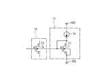
(第1の実施の形態)
図1は、本発明の第1の実施の形態に係る半導体回路の構成を示す回路図である。
この半導体回路におけるしきい値電圧の調整について説明する。本半導体回路は、MOSトランジスタ(単に、トランジスタとも略す)T1及び電流源Iaを有するバルク電位制御回路11と、トランジスタT2による被バルク電位制御MOSトランジスタ(被制御トランジスタとも略す)10と備えて構成されている。
トランジスタT1のゲート端子g及びドレイン端子dと、トランジスタT2のバルク端子bとは電流源Iaに接続されており、トランジスタT1のソース端子はソース電源VSSに接続されている。
(First embodiment)
FIG. 1 is a circuit diagram showing a configuration of a semiconductor circuit according to the first embodiment of the present invention.
Adjustment of the threshold voltage in this semiconductor circuit will be described. The semiconductor circuit includes a bulk
The gate terminal g and drain terminal d of the transistor T1 and the bulk terminal b of the transistor T2 are connected to the current source Ia, and the source terminal of the transistor T1 is connected to the source power supply VSS.
一般にトランジスタのしきい値電圧は、Vth=k√(2ΦF+Vbs)+VFB+2ΦFの式で表される。ここでk:基板定数、ΦF:フェルミポテンシャル、Vbs:ソース−バルク間電圧、VFB:フラットバンド電圧である。
これをグラフに表すと図2のようになるが、ソース−バルク間電圧Vbsのある領域に限ればおよそ直線近似で表す事ができ、破線で示すように動作時のしきい値電圧Vth=VT+γVbs(γ:直線近似時の基板係数)となる。
In general, the threshold voltage of a transistor is expressed by the following equation: Vth = k√ (2Φ F + Vbs) + V FB + 2Φ F. Here, k: substrate constant, Φ F : Fermi potential, Vbs: source-bulk voltage, and V FB : flat band voltage.
This can be represented in a graph as shown in FIG. 2, but can be represented by a linear approximation as long as it is limited to a region where the source-bulk voltage Vbs is present, and the threshold voltage Vth = V during operation as shown by the broken line. T + γVbs (γ: substrate coefficient in linear approximation).
MOSが飽和領域で動作している場合、ドレイン電流Idsとゲート−ソース間電圧Vgsとの間には、Ids=K×(W/L)×(Vgs−Vth)2が成り立つ。K:飽和領域でのゲインファクターである。
このことから、電流源Iaから供給されるトランジスタT1のドレイン電流をIds1とすると、Ids1=K×(W1/L1)×(Vgs1−VT1)2であり、トランジスタT1のゲート電位はVg1=Vgs1=VT1+√{Ids1/(K×W1/L1)}のようになる。
When the MOS operates in the saturation region, Ids = K × (W / L) × (Vgs−Vth) 2 is established between the drain current Ids and the gate-source voltage Vgs. K: Gain factor in the saturation region.
Therefore, when the drain current of the transistor T1 supplied from the current source Ia and Ids1, Ids1 = K × (W1 / L1) × (Vgs1-V T 1) is 2, the gate potential of the transistor T1 is Vg1 = Vgs1 = V T 1 + √ {Ids1 / (K × W1 / L1)}
ここで√{Ids1/(K×W1/L1)}=α1と置くと、トランジスタT2のバルク端子bはトランジスタT1のゲート端子gに接続されていることから、トランジスタT2のバルク電位はVb2=Vg1=VT1+α1であり、トランジスタT2のソース−バルク間電圧はVbs2=Vs2−(VT1+α1)となる。
トランジスタT2のしきい値電圧Vth2は、Vth=VT+γVbsに従ってソース−バルク間電圧Vbsにより変化し、Vth2=VT2+γVbs2=VT2+γ(Vs2−VT1−α1)となる。
Here, when √ {Ids1 / (K × W1 / L1)} = α1, since the bulk terminal b of the transistor T2 is connected to the gate terminal g of the transistor T1, the bulk potential of the transistor T2 is Vb2 = Vg1. = V T 1 + α1, and the source-bulk voltage of the transistor T2 is Vbs2 = Vs2− (V T 1 + α1).
The threshold voltage Vth2 of the transistor T2 changes according to the source-bulk voltage Vbs according to Vth = V T + γVbs, and becomes Vth2 = V T 2 + γVbs2 = V T 2 + γ (Vs2−V T 1−α1).
ここでトランジスタT1及びT2をVT1=VT2となるように選択すると、Vth2=(1−γ)×VT2+γ×(Vs2−α1)となり、|1−γ|<1であればトランジスタT1によるバルク電位制御により、トランジスタT2の動作時のしきい値電圧Vthの絶対値及びばらつき幅は、Vbs=0の時のしきい値電圧VTに対して減じられたものとなる。 Selecting where the transistors T1 and T2 such that V T 1 = V T 2, Vth2 = (1-γ) × V T 2 + γ × (Vs2-α1) next, | if <a 1 | 1-gamma the bulk potential control of the transistors T1, absolute value and variation width of the threshold voltage Vth during the operation of the transistor T2 becomes as being reduced with respect to the threshold voltage V T when the Vbs = 0.
このように第1の実施の形態の半導体回路によれば、被制御側のMOSトランジスタT2に、バルク電位制御用のMOSトランジスタT1のしきい値電圧VTに応じたバルク電位を与えることで、MOSトランジスタT2のしきい値電圧Vthの絶対値及びしきい値電圧のばらつき幅の双方を低減させることができる。 Thus according to the semiconductor circuit of the first embodiment, the MOS transistor T2 of the control side, to provide a bulk potential corresponding to the threshold voltage V T of the MOS transistor T1 for bulk potential control, Both the absolute value of the threshold voltage Vth of the MOS transistor T2 and the variation width of the threshold voltage can be reduced.
(第2の実施の形態)
図3は、本発明の第2の実施の形態に係る半導体回路の構成を示す回路図である。
この半導体回路におけるしきい値電圧の調整について説明する。本半導体回路は、MOSトランジスタT3,T4及び電流源Ibを有するバルク電位制御回路31と、トランジスタT5による被制御トランジスタ30とを備えて構成されている。
トランジスタT3及びT4は各々自体のゲート端子g及びドレイン端子dが短絡されており(ダイオード接続)、トランジスタT3のドレイン端子dは電流源Ibに接続され、トランジスタT4のソース端子sはVSSに接地されている。
(Second Embodiment)
FIG. 3 is a circuit diagram showing a configuration of a semiconductor circuit according to the second embodiment of the present invention.
Adjustment of the threshold voltage in this semiconductor circuit will be described. This semiconductor circuit includes a bulk
Each of the transistors T3 and T4 has its gate terminal g and drain terminal d short-circuited (diode connection), the drain terminal d of the transistor T3 is connected to the current source Ib, and the source terminal s of the transistor T4 is grounded to VSS. ing.
更に、トランジスタT3のソース端子sとトランジスタT4のドレイン端子dは直接接続されるか、もしくはトランジスタのしきい値電圧の総和が電源電圧を超えない範囲で両者の間に図示せぬダイオード接続型トランジスタを複数挿入することが可能である。図3に直列にn個接続された状態を示した。トランジスタT5のバルク端子bはトランジスタT3のドレイン端子dと接続されている。
電流源Ib及びn個の直列接続されたダイオード接続型トランジスタT3,…,T4の回路がバルク電位制御回路31であり、トランジスタT5が被バルク電位制御MOSトランジスタ30である。
Further, the source terminal s of the transistor T3 and the drain terminal d of the transistor T4 are directly connected, or a diode-connected transistor (not shown) between them as long as the sum of the threshold voltages of the transistors does not exceed the power supply voltage. It is possible to insert more than one. FIG. 3 shows a state in which n pieces are connected in series. The bulk terminal b of the transistor T5 is connected to the drain terminal d of the transistor T3.
A circuit of the current source Ib and n diode-connected transistors T3,..., T4 connected in series is a bulk
n個の直列接続されたダイオード接続型トランジスタT3,…,T4は、全て同じサイズW3,L3及びしきい値電圧VT3であり、直列接続され且つドレイン電流も等しいことからトランジスタT3のゲート電位はVg3=n×(VT3+α3)となる。但し、α3=√{Ids3/(K×W3/L3)}。よってトランジスタT5のソース−バルク間電圧Vbs5=Vs5−n×(VT3+α3)となる。 The n series-connected diode-connected transistors T3,..., T4 are all the same size W3, L3 and threshold voltage V T3 , and are connected in series and have the same drain current. Vg3 = n × (V T 3 + α3). However, α3 = √ {Ids3 / (K × W3 / L3)}. Therefore, the source-bulk voltage Vbs5 of the transistor T5 = Vs5-n × (V T 3 + α3).
また、Vth5=VT5+γVbs5=VT5+γ{Vs5−n×(VT3+α3)}であるが、トランジスタT3及びT5をVT3=VT5となるように選択すると、Vth5=(1−γ×n)×VT5+γ(Vs5−n×α3)となる。
このように第2の実施の形態の半導体回路によれば、上記第1の実施の形態で得られるしきい値電圧の絶対値及びばらつき幅の低減効果が小さすぎて所望のものでない場合、その効果を増大させることができる。
Further, Vth5 = V T 5 + γVbs5 = V T 5 + γ is a {Vs5-n × (V T 3 + α3)}, by selecting the transistors T3 and T5 such that V T 3 = V T 5, Vth5 = (1- γ × n) × V T 5 + γ (Vs5−n × α3).
As described above, according to the semiconductor circuit of the second embodiment, if the effect of reducing the absolute value and variation width of the threshold voltage obtained in the first embodiment is too small to be desired, The effect can be increased.
(第3の実施の形態)
図4は、本発明の第3の実施の形態に係る半導体回路の構成を示す回路図である。
この半導体回路におけるしきい値電圧の調整について説明する。本半導体回路は、MOSトランジスタT6と、電流源Icと、抵抗器Ra及びRbとを有するバルク電位制御回路41と、トランジスタT7による被制御トランジスタ40とを備えて構成されている。
(Third embodiment)
FIG. 4 is a circuit diagram showing a configuration of a semiconductor circuit according to the third embodiment of the present invention.
Adjustment of the threshold voltage in this semiconductor circuit will be described. This semiconductor circuit includes a MOS transistor T6, a current source Ic, a bulk
トランジスタT6のゲート端子g、ドレイン端子dは電流源Iaに接続されており、トランジスタT6のソース端子sはVSSに接続されている。抵抗器Ra及びRbは互いに直列に接続され、抵抗器Raの他方の端子はトランジスタT6のゲート端子gに接続され、抵抗器Rbの他方の端子はVSSに接続されており、抵抗器Ra・Rb間の接続部分はトランジスタT7のバルク端子bに接続され、当該接続部分はトランジスタT6のゲート端子gの電位を分割した電位を出力している。 The gate terminal g and the drain terminal d of the transistor T6 are connected to the current source Ia, and the source terminal s of the transistor T6 is connected to VSS. The resistors Ra and Rb are connected in series, the other terminal of the resistor Ra is connected to the gate terminal g of the transistor T6, the other terminal of the resistor Rb is connected to VSS, and the resistors Ra and Rb The connecting portion is connected to the bulk terminal b of the transistor T7, and the connecting portion outputs a potential obtained by dividing the potential of the gate terminal g of the transistor T6.
トランジスタT6のゲート電位は、上記第1の実施の形態と同様にVg6=VT6+α6となる。ただしα6=√{Ids6/(K×W6/L6)}。抵抗器Ra及びRbの抵抗分割によりトランジスタT7のバルク電位はVb7=Rb/(Ra+Rb)×(VT6+α6)となり、ソース−バルク間電圧Vbs7=Vs7−Rb/(Ra+Rb)×(VT6+α6)となる。
Vth7=VT7+γVbs7=VT7+γ{Vs7−Rb/(Ra+Rb)×(VT6+α6)}であるが、トランジスタT6及びT7をVT6=VT7となるように選択すると、Vth7={1−γ×Rb/(Ra+Rb)}×VT7+γ{Vs7−Rb/(Ra+Rb)×α6}となる。
The gate potential of the transistor T6 is Vg6 = V T 6 + α6 as in the first embodiment. However, α6 = √ {Ids6 / (K × W6 / L6)}. Due to the resistance division of the resistors Ra and Rb, the bulk potential of the transistor T7 becomes Vb7 = Rb / (Ra + Rb) × (V T 6 + α6), and the source-bulk voltage Vbs7 = Vs7−Rb / (Ra + Rb) × (V T 6 + α6) It becomes.
Vth7 =
このように第3の実施の形態の半導体回路によれば、上記第1の実施の形態で得られるしきい値電圧の絶対値及びばらつき幅の低減効果が大きすぎ所望のものでない場合、その効果を減少させることができる。
但し、上記では抵抗器Ra及びRbの互いの接続端子以外の他の端子は、トランジスタT6のドレイン端子dと、VSSとの間に接続したが、この他に、同ドレイン端子dと、電源電位、接地電位と電源電位との任意の分割電位、任意の固定電位の何れか1つの電位を有する端子との間に接続してもよい。
As described above, according to the semiconductor circuit of the third embodiment, if the effect of reducing the absolute value and variation width of the threshold voltage obtained in the first embodiment is too large and not desired, the effect is obtained. Can be reduced.
However, in the above description, the terminals other than the connection terminals of the resistors Ra and Rb are connected between the drain terminal d of the transistor T6 and VSS. The terminal may be connected between a terminal having any one potential of any divided potential of the ground potential and the power supply potential and any fixed potential.
(第4の実施の形態)
図5は、本発明の第4の実施の形態に係る半導体回路の構成を示す回路図である。
この半導体回路におけるしきい値電圧の調整について説明する。本半導体回路は、MOSトランジスタT8と、電流源Idと、抵抗器Rc及びRdとを有するバルク電位制御回路51と、トランジスタT9による被制御トランジスタ50とを備えて構成されている。
トランジスタT8のゲート端子gはドレイン端子dに短絡されており、ドレイン端子dは電流源Idに接続され、ソース端子sはVSSに接地されている。
(Fourth embodiment)
FIG. 5 is a circuit diagram showing a configuration of a semiconductor circuit according to the fourth embodiment of the present invention.
Adjustment of the threshold voltage in this semiconductor circuit will be described. This semiconductor circuit includes a MOS transistor T8, a current source Id, a bulk
The gate terminal g of the transistor T8 is short-circuited to the drain terminal d, the drain terminal d is connected to the current source Id, and the source terminal s is grounded to VSS.
抵抗器Rc及びRdは直列に接続されており、抵抗器Rcの他方の端子は電源電圧VDDに、抵抗器Rdの他方の端子はトランジスタT8のドレイン端子dにそれぞれ接続され、抵抗器Rc・Rd間の端子は電源電圧VDDとトランジスタT8のゲート端子の電位を分割した電位を出力している。トランジスタT9のバルク端子bは抵抗器Rc・Rd間の端子と接続されている。 The resistors Rc and Rd are connected in series, the other terminal of the resistor Rc is connected to the power supply voltage VDD, the other terminal of the resistor Rd is connected to the drain terminal d of the transistor T8, and the resistors Rc and Rd are connected. The terminal between them outputs a potential obtained by dividing the power supply voltage VDD and the potential of the gate terminal of the transistor T8. The bulk terminal b of the transistor T9 is connected to the terminal between the resistors Rc and Rd.
トランジスタT8のゲート電位は、上記第1の実施の形態と同様にVg8=VT8+α8となる。但し、α8=√{Ids8/(K×W8/L8)}。抵抗器Rc及びRdによる抵抗分割によりトランジスタT9のバルク電位はVb9=Rc/(Rc+Rd)×(VT8+α8)+Rd/(Rc+Rd)×VDDとなり、ソース−バルク間電圧はVbs9=Vs9−Rc/(Rc+Rd)×(VT8+α8)−Rd/(Rc+Rd)×VDDとなる。 The gate potential of the transistor T8 is Vg8 = V T 8 + α8 as in the first embodiment. However, α8 = √ {Ids8 / (K × W8 / L8)}. Due to the resistance division by the resistors Rc and Rd, the bulk potential of the transistor T9 becomes Vb9 = Rc / (Rc + Rd) × (V T 8 + α8) + Rd / (Rc + Rd) × VDD, and the source-bulk voltage is Vbs9 = Vs9−Rc / ( Rc + Rd) × (V T 8 + α8) −Rd / (Rc + Rd) × VDD.
Vth9=VT9+γVbs9=VT9+γ{Vs9−Rc/(Rc+Rd)×(VT8+α8)−Rd/(Rc+Rd)×VDD}であるが、トランジスタT8及びT9をVT8=VT9となるように選択すると、Vth9={1−γ×Rc/(Rc+Rd)}×VT9+γ{Vs9−Rc/(Rc+Rd)×α8−Rd/(Rc+Rd)×VDD}となる。 Vth9 = V T 9 + γVbs9 = V T 9 + γ {Vs9-Rc / (Rc + Rd) × (V T 8 + α8) -Rd / (Rc + Rd) × VDD} is a, consisting of the transistors T8 and T9 and V T 8 = V T 9 Thus, Vth9 = {1−γ × Rc / (Rc + Rd)} × V T 9 + γ {Vs9−Rc / (Rc + Rd) × α8−Rd / (Rc + Rd) × VDD}.
抵抗器Rcの端子に接続されている電源電圧VDDは、VDDとVSSの任意の分割電位、電源電圧に依存しない固定電位でもよく、参照する電位を変える事で、しきい値電圧Vth9にはVT9に依存しない任意のオフセット量をもたせることができる。
このように第4の実施の形態の半導体回路によれば、上記第1の実施の形態で得られるしきい値電圧の絶対値及びばらつき幅の低減効果が所望のものでない場合、その効果を調整することができる。
The power supply voltage VDD connected to the terminal of the resistor Rc may be an arbitrary divided potential of VDD and VSS, or a fixed potential that does not depend on the power supply voltage. By changing the reference potential, the threshold voltage Vth9 is set to V You can have a desired offset that is independent of T 9.
As described above, according to the semiconductor circuit of the fourth embodiment, if the effect of reducing the absolute value and the variation width of the threshold voltage obtained in the first embodiment is not desired, the effect is adjusted. can do.
(第5の実施の形態)
図6は、本発明の第5の実施の形態に係る半導体回路の構成を示す回路図である。
この半導体回路におけるしきい値電圧の調整について説明する。本半導体回路は、MOSトランジスタT10,T11と、電流源Ieと、抵抗器Rc及びRdとを有するバルク電位制御回路61と、トランジスタT12による被制御トランジスタ60とを備えて構成されている。
トランジスタT10及びT11は、各々自体のゲート端子g及びドレイン端子dが短絡されており(ダイオード接続)、トランジスタT10のドレイン端子dは電流源Ieに接続され、トランジスタT11のソース端子sはVSSに接地されている。
(Fifth embodiment)
FIG. 6 is a circuit diagram showing a configuration of a semiconductor circuit according to the fifth embodiment of the present invention.
Adjustment of the threshold voltage in this semiconductor circuit will be described. This semiconductor circuit includes MOS transistors T10 and T11, a current source Ie, a bulk
Each of the transistors T10 and T11 has its gate terminal g and drain terminal d short-circuited (diode connection), the drain terminal d of the transistor T10 is connected to the current source Ie, and the source terminal s of the transistor T11 is grounded to VSS. Has been.
更に、トランジスタT10のソース端子sとトランジスタT11のドレイン端子dは直接接続されるか、もしくは電源電圧を超えない範囲で両者の間に同様のダイオード接続型トランジスタを複数挿入することが可能である。図6に直列にn個接続された状態を示した。
抵抗器Re及びRfは互いに直列に接続され、抵抗器Reの他方の端子はトランジスタT10のゲート端子に接続され、抵抗器Rfの他方の端子はVSSに接続されており、抵抗器Re・Rf間の接続部分はトランジスタT10のゲート端子の電位を分割した電位を出力している。トランジスタT12のバルク端子bは抵抗器Re・Rf間の接続部分と接続されている。
Further, the source terminal s of the transistor T10 and the drain terminal d of the transistor T11 are directly connected, or a plurality of similar diode-connected transistors can be inserted between the two so long as the power supply voltage is not exceeded. FIG. 6 shows a state where n pieces are connected in series.
Resistors Re and Rf are connected in series with each other, the other terminal of the resistor Re is connected to the gate terminal of the transistor T10, the other terminal of the resistor Rf is connected to VSS, and between the resistors Re and Rf Are connected to output a potential obtained by dividing the potential of the gate terminal of the transistor T10. The bulk terminal b of the transistor T12 is connected to a connection portion between the resistors Re and Rf.
n個の直列接続されたダイオード接続型トランジスタは全て同じサイズW10,L10及びしきい値電圧VT10であり、直列接続されドレイン電流も等しいことからトランジスタT10のゲート電位はVg10=n×(VT10+α10)となる。
但し、α10=√{Ids10/(K×W10/L10)}。抵抗器Re及びRfの抵抗分割によりトランジスタT12のバルク電位はVb12=n×Rf/(Re+Rf)×(VT10+α10)となり、ソース−バルク間電圧はbs12=Vs12−n×Rf/(Re+Rf)×(VT10+α10)となる。
Since all the n diode-connected transistors connected in series have the same size W10, L10 and
However, α10 = √ {Ids10 / (K × W10 / L10)}. By dividing the resistors Re and Rf, the bulk potential of the transistor T12 becomes Vb12 = n × Rf / (Re + Rf) × (
Vth12=VT12+γVbs12=VT12+γ{Vs12−n×Rf/(Re+Rf)×(VT10+α10)}であるが、トランジスタT10及びT12をT10=VT12となるように選択すると、Vth12={1−γ×n×Rf/(Re+Rf)}×VT12+γ{Vs12−n×Rf/(Re+Rf)×α10}となる。
また、本実施の形態についても上記第3の実施の形態で述べたように、抵抗器の接続先を接地電位VSSから電源電圧VDD、もしくはVDDとVSSの任意の分割電位、電源電圧に依存しない固定電位の何れかに変更してもよく、このように参照する電位を変える事で、しきい値電圧Vth12にはVT12に依存しない任意のオフセット量をもたせることができる。
このように第5の実施の形態の半導体回路によれば、上記第1の実施の形態で得られるしきい値電圧の絶対値及びばらつき幅の低減効果が大き過ぎるもしくは小さ過ぎるなど所望のものでない場合、その効果を調整することができる。
Vth12 = V T 12 + γVbs12 = V T 12 + γ is a {Vs12-n × Rf / ( Re + Rf) × (
Also in this embodiment, as described in the third embodiment, the connection destination of the resistor does not depend on the ground potential VSS to the power supply voltage VDD, or any divided potential between VDD and VSS, and the power supply voltage. may be changed to any fixed potential, by changing a potential referencing this manner, the threshold voltage Vth12 can have a desired offset that is independent of V T 12.
As described above, according to the semiconductor circuit of the fifth embodiment, the effect of reducing the absolute value and variation width of the threshold voltage obtained in the first embodiment is not desirable, such as too large or too small. If so, the effect can be adjusted.
(第6の実施の形態)
図7は、本発明の第6の実施の形態に係る半導体回路の構成を示す回路図である。
この半導体回路におけるしきい値電圧の調整について説明する。本半導体回路は、MOSトランジスタT13及び電流源Ifを有するバルク電位制御回路71と、トランジスタT14,T15,T16による被制御トランジスタ70とを備えて構成されている。
トランジスタT13及び電流源Ifは、それぞれ図1に示したトランジスタT1及び電流源Iaに該当し、トランジスタT14、T15及びT16は図1のトランジスタT2に該当しており、同じ回路構成となっている。異なる個所は、トランジスタT14、T15及びT16のソース端子がVSSに接地されていることである。
(Sixth embodiment)
FIG. 7 is a circuit diagram showing a configuration of a semiconductor circuit according to the sixth embodiment of the present invention.
Adjustment of the threshold voltage in this semiconductor circuit will be described. This semiconductor circuit includes a bulk
The transistor T13 and the current source If correspond to the transistor T1 and the current source Ia shown in FIG. 1, respectively. The transistors T14, T15, and T16 correspond to the transistor T2 in FIG. 1, and have the same circuit configuration. The difference is that the source terminals of transistors T14, T15 and T16 are grounded to VSS.
上記第1の実施の形態で説明したようにVs2=0に当たるため、トランジスタT14、T15及びT16のVTが等しければ、しきい値電圧も等しくVth14,15,16=(1−γ)×VT14−γ×α13となり、|1−γ|<1であればしきい値電圧の絶対値及びばらつき幅を減ずる事ができる。
また、トランジスタT13及び電流源Ifで構成されるバルク電位制御回路71は、図4に示したバルク電位制御回路41でもよく、しきい値電圧の低減効果を調整することが可能である。
Since striking the Vs2 = 0 as described in the first embodiment, the transistor T14, being equal V T of T15 and T16, the threshold voltage equal Vth14,15,16 = (1-γ) × V T 14-γ × α13 next, | 1-gamma | if <1 can reduce the absolute value and the variation width of the threshold voltage.
Further, the bulk
これらのことから、第6の実施の形態の半導体回路によれば、デジタル回路等が低電圧電源であっても、動作マージンを得ることができる。
上述のように、第1〜第6の実施の形態の半導体回路においては、バルク電位制御回路を付加していない半導体回路に比べ、低電源電圧時の動作マージンを持たせることができる。
また、従来技術に比べ構成が簡便で回路面積を小さくすることができ、低電圧動作に向くので安定した低電圧動作を行うことができ、しきい値電圧Vthの変動に対して連続的に制御がかかり、使用可能な半導体回路の範囲が広くなるなどの効果がある。
For these reasons, according to the semiconductor circuit of the sixth embodiment, an operation margin can be obtained even if the digital circuit or the like is a low-voltage power supply.
As described above, the semiconductor circuits of the first to sixth embodiments can have an operation margin at the time of a low power supply voltage as compared with a semiconductor circuit to which no bulk potential control circuit is added.
Compared with the prior art, the configuration is simple, the circuit area can be reduced, and since it is suitable for low-voltage operation, stable low-voltage operation can be performed, and continuous control is performed against fluctuations in the threshold voltage Vth. As a result, the range of usable semiconductor circuits is widened.
(第7の実施の形態)
図8は、本発明の第7の実施の形態に係る被制御トランジスタが差動増幅回路である場合の半導体回路の構成を示す回路図である。
本半導体回路は、MOSトランジスタT17及び電流源Igを有するバルク電位制御回路81と、差動対のトランジスタT18,T19による被制御トランジスタ80と、電流源Ihとを備えて構成されている。トランジスタT17及び電流源Igはそれぞれ図1のトランジスタT1及び電流源Iaに該当し、同じ回路構成となっている。
差動対のトランジスタT18,T19は、互いのバルク端子b及びソース端子sがそれぞれ結合されており、それらのバルク端子bがトランジスタT17のゲート端子gに接続され、ソース端子sが電流源Ihを介してVSSに接続されている。
(Seventh embodiment)
FIG. 8 is a circuit diagram showing a configuration of a semiconductor circuit when the controlled transistor according to the seventh embodiment of the present invention is a differential amplifier circuit.
This semiconductor circuit includes a bulk
In the differential pair of transistors T18 and T19, the bulk terminal b and the source terminal s are coupled to each other, the bulk terminal b is connected to the gate terminal g of the transistor T17, and the source terminal s is connected to the current source Ih. To VSS.
入力電圧をVinとすると、差動対の一方のトランジスタT18に流れるドレイン電流は、飽和領域下においてIds18=K×W18/L18×(Vin−Vs18−Vth18)2となる。よってVs18=Vin−Vth18−α18である。
また、差動対のトランジスタT18,T19をVT17=VT18となるように選択すると、Vth18=VT18+γ(Vs18−VT18−α17)であり、しきい値電圧Vth18が減じるとソース電位Vs18が上がり、更にしきい値電圧Vth18が減じる事になる。この結果、Vth18=(1−γ)/(1+γ)×VT18+γ/(1+γ)×(Vin−α18−α17)となり、しきい値電圧のばらつき幅を特に抑制することができる。
When the input voltage is Vin, the drain current flowing through one transistor T18 of the differential pair is Ids18 = K × W18 / L18 × (Vin−Vs18−Vth18) 2 under the saturation region. Therefore, Vs18 = Vin−Vth18−α18.
Further, when the differential pair transistors T18 and T19 are selected so that V T 17 = V T 18 is satisfied, Vth 18 = V T 18 + γ (Vs18−V T 18−α17), and the threshold voltage Vth18 decreases. The source potential Vs18 is increased, and the threshold voltage Vth18 is further decreased. As a result, Vth18 = (1−γ) / (1 + γ) × V T 18 + γ / (1 + γ) × (Vin−α18−α17), and the variation width of the threshold voltage can be particularly suppressed.
また、トランジスタT17及び電流源Igで構成されるバルク電位制御回路81は、図4に示したバルク電位制御回路41でもよく、しきい値電圧の低減効果を調整することが可能である。
従って、第7の実施の形態の半導体回路によれば、差動増幅回路を低電圧電源での動作に有利な回路とすることができる。
Further, the bulk
Therefore, according to the semiconductor circuit of the seventh embodiment, the differential amplifier circuit can be an advantageous circuit for operation with a low-voltage power supply.
(第8の実施の形態)
図9は、本発明の第8の実施の形態に係る被制御トランジスタが電流ミラー回路である場合の半導体回路の構成を示す回路図である。
本半導体回路は、MOSトランジスタT20及び電流源Iiを有するバルク電位制御回路91と、一対のトランジスタT21,T22による被制御トランジスタ90と、電流源Ijとを備えて構成されている。トランジスタT20及び電流源Iiはそれぞれ図1のトランジスタT1及び電流源Iaに該当し、同じ回路構成となっている。
(Eighth embodiment)
FIG. 9 is a circuit diagram showing a configuration of a semiconductor circuit when the controlled transistor according to the eighth embodiment of the present invention is a current mirror circuit.
The semiconductor circuit includes a bulk
一対のトランジスタT21,T22は、互いのゲート端子gが接続され、これらゲート端子gが一方のトランジスタT21のドレイン端子dと共に電流源Ijを介して電源VDDに接続され、また、互いのバルク端子bがトランジスタT20のゲート端子gに接続され、更に、互いのソース端子sがVSSに接地されており、即ち、電流ミラー回路構成とされている。 The pair of transistors T21 and T22 have their gate terminals g connected to each other, and these gate terminals g are connected to the power supply VDD via the current source Ij together with the drain terminal d of the one transistor T21. Are connected to the gate terminal g of the transistor T20, and the source terminals s of the transistors T20 are grounded to VSS, that is, a current mirror circuit configuration is formed.
飽和領域下であればトランジスタT21及びT22に流れる電流量Ids21及びIds22は等しくなるが、Vds21=Vth21+α21=(1−γ)×VT21−γ×α20+α21であることから、|1−γ|<1であればしきい値電圧の絶対値及びばらつき幅を減ずる事ができる。
また、トランジスタT20及び電流源Iiで構成されるバルク電位制御回路91は、図4に示したバルク電位制御回路41でもよく、しきい値電圧の低減効果を調整することが可能である。
従って、第8の実施の形態の半導体回路によれば、電流ミラー回路を低電圧電源での動作に有利な回路とすることができる。
Becomes equal current amount Ids21 and Ids22 flowing through the transistors T21 and T22 if under the saturation region, since it is Vds21 = Vth21 + α21 = (1 -γ) × V T 21-γ × α20 + α21, | 1-γ | < If it is 1, the absolute value and variation width of the threshold voltage can be reduced.
Further, the bulk
Therefore, according to the semiconductor circuit of the eighth embodiment, the current mirror circuit can be an advantageous circuit for operation with a low voltage power supply.
(第9の実施の形態)
図10は、本発明の第9の実施の形態に係る被制御トランジスタがソースフォロワ回路である場合の半導体回路の構成を示す回路図である。
本半導体回路は、MOSトランジスタT23及び電流源Ikを有するバルク電位制御回路101と、トランジスタT24による被制御トランジスタ90と、電流源Ilとを備えて構成されている。トランジスタT23及び電流源Ilはそれぞれ図1のトランジスタT1及び電流源Iaに該当し、同じ回路構成となっている。
トランジスタT24のソース端子は、電流源Ilを介してVSSに接地されることによってソースフォロワ回路構成とされている。
(Ninth embodiment)
FIG. 10 is a circuit diagram showing a configuration of a semiconductor circuit when the controlled transistor according to the ninth embodiment of the present invention is a source follower circuit.
This semiconductor circuit includes a bulk
The source terminal of the transistor T24 is grounded to VSS via the current source Il, thereby forming a source follower circuit configuration.
トランジスタT24が飽和領域下で動作している場合、ソース電位Vs24はゲート電位Vgよりしきい値電圧Vth24以上低くなるので、バルク電位制御回路101を付加してない場合に比べてソース電位Vs24を大きくすることができ、低電圧動作に有利なソースフォロワ回路100となる。
また、トランジスタT23及び電流源Ikで構成されるバルク電位制御回路101は、図4に示したバルク電位制御回路41でもよく、しきい値電圧の低減効果を調整することが可能である。
When the transistor T24 operates under the saturation region, the source potential Vs24 is lower than the gate potential Vg by the threshold voltage Vth24 or more, so that the source potential Vs24 is set larger than when the bulk
Further, the bulk
10,30,40,50,60,70,80,90,100 被バルク電位制御MOSトランジスタ(被制御トランジスタ)
11,31,41,51,61,71,81,91,101 バルク電位制御回路
T1,T3,T4,T6,T8,T10,T11,T13,T17,T20,T23 バルク電位制御側のMOSトランジスタ
T2,T5,T7,T9,T12,T14,T15,T16,T18,T19,T21,T22,T24 被バルク電位制御側のMOSトランジスタ
Ra,Rb,Rc,Rd,Re,Rf 抵抗器
Ia,Ib,Ic,Id,Ie,If,Ig,Ih,Ii,Ij,Ik,Il 電流源
VDD 電源
VSS アース
10, 30, 40, 50, 60, 70, 80, 90, 100 Bulk potential controlled MOS transistor (controlled transistor)
11, 31, 41, 51, 61, 71, 81, 91, 101 Bulk potential control circuit T1, T3, T4, T6, T8, T10, T11, T13, T17, T20, T23 Bulk potential control side MOS transistor T2 , T5, T7, T9, T12, T14, T15, T16, T18, T19, T21, T22, T24 MOS transistors Ra, Rb, Rc, Rd, Re, Rf on the bulk potential control side Resistors Ia, Ib, Ic , Id, Ie, If, Ig, Ih, Ii, Ij, Ik, Il Current source VDD Power supply VSS Ground
Claims (9)
前記第1のMOSトランジスタと同伝導型で且つ第1のMOSトランジスタのドレイン端子に、バルク端子が接続された第2のMOSトランジスタと、
前記第1のMOSトランジスタのドレイン端子に接続され、当該第1のMOSトランジスタに電流を供給する電流源とを備え、
前記第1のMOSトランジスタのソース端子は、電源端子に電気的に接続され、
前記第1のMOSトランジスタのドレイン端子及び前記第2のMOSトランジスタのバルク端子は、当該第1のMOSトランジスタのしきい値電圧に応じた電位を有することを特徴とする半導体回路。 A first MOS transistor in which the gate terminal and the drain terminal are short-circuited , and the same potential is supplied to the bulk terminal and the source terminal ;
A second MOS transistor having the same conductivity type as the first MOS transistor and having a bulk terminal connected to the drain terminal of the first MOS transistor;
A current source connected to the drain terminal of the first MOS transistor and supplying a current to the first MOS transistor;
A source terminal of the first MOS transistor is electrically connected to a power supply terminal;
A semiconductor circuit, wherein a drain terminal of the first MOS transistor and a bulk terminal of the second MOS transistor have a potential corresponding to a threshold voltage of the first MOS transistor.
接地電位、電源電位、接地電位と電源電位との任意の分割電位、電源電位に依存しない任意の固定電位、前記第1のMOSトランジスタのソース電位の何れか1つの電位と、前記第1のMOSトランジスタのドレイン端子の電位とを分割するように接続された分割抵抗器と、
前記第1のMOSトランジスタと同伝導型であって前記分割抵抗器の分割電位の出力端子に接続されたバルク端子を有する第2のMOSトランジスタと、
前記第1のMOSトランジスタのドレイン端子に接続され、当該第1のMOSトランジスタに電流を供給する電流源と、
を備え、
前記第1のMOSトランジスタのソース端子は、電源端子に電気的に接続されることを特徴とする半導体回路。 A first MOS transistor in which the gate terminal and the drain terminal are short-circuited , and the same potential is supplied to the bulk terminal and the source terminal ;
Any one of a ground potential, a power supply potential, an arbitrary divided potential between the ground potential and the power supply potential, an arbitrary fixed potential independent of the power supply potential, a source potential of the first MOS transistor, and the first MOS A dividing resistor connected to divide the potential of the drain terminal of the transistor;
A second MOS transistor having the same conductivity type as the first MOS transistor and having a bulk terminal connected to the output terminal of the divided potential of the dividing resistor;
A current source connected to the drain terminal of the first MOS transistor and supplying a current to the first MOS transistor ;
Equipped with a,
A semiconductor circuit, wherein a source terminal of the first MOS transistor is electrically connected to a power supply terminal .
ことを特徴とする請求項1から5の何れか1項に記載の半導体回路。 A plurality of the second MOS transistors are used as the second MOS transistors, the bulk terminals of these transistor groups are connected to the drain terminals of the first transistors, and the source terminals of the second transistor groups are connected to each other. The semiconductor circuit according to any one of claims 1 to 5, wherein the semiconductor circuit is characterized in that:
ことを特徴とする請求項1から5の何れか1項に記載の半導体回路。 Two second MOS transistors are used as the second MOS transistors, the bulk terminals and the source terminals are coupled to each other, each bulk terminal is connected to the drain terminal of the first MOS transistor, and each source is connected. 6. The semiconductor circuit according to claim 1, wherein a terminal is connected to the power supply terminal via a second current source.
ことを特徴とする請求項6に記載の半導体回路。 Connect the gate terminal of the transistor group with one another, connect the drain terminal of one of the transistors of the transistor group to these gate terminal connected to said power supply terminal of the connection point through the third current source The semiconductor circuit according to claim 6, wherein the semiconductor circuit has a connected current mirror circuit configuration.
ことを特徴とする請求項1から5の何れか1項に記載の半導体回路。 The semiconductor circuit according to any one of claims 1 to 5, characterized in that a source follower circuit constituting the source terminal via a fourth current source connected to said power supply terminal of said second MOS transistor .
Priority Applications (1)
| Application Number | Priority Date | Filing Date | Title |
|---|---|---|---|
| JP2005138776A JP4620522B2 (en) | 2005-05-11 | 2005-05-11 | Semiconductor circuit |
Applications Claiming Priority (1)
| Application Number | Priority Date | Filing Date | Title |
|---|---|---|---|
| JP2005138776A JP4620522B2 (en) | 2005-05-11 | 2005-05-11 | Semiconductor circuit |
Publications (2)
| Publication Number | Publication Date |
|---|---|
| JP2006319557A JP2006319557A (en) | 2006-11-24 |
| JP4620522B2 true JP4620522B2 (en) | 2011-01-26 |
Family
ID=37539838
Family Applications (1)
| Application Number | Title | Priority Date | Filing Date |
|---|---|---|---|
| JP2005138776A Expired - Fee Related JP4620522B2 (en) | 2005-05-11 | 2005-05-11 | Semiconductor circuit |
Country Status (1)
| Country | Link |
|---|---|
| JP (1) | JP4620522B2 (en) |
Families Citing this family (1)
| Publication number | Priority date | Publication date | Assignee | Title |
|---|---|---|---|---|
| CN101510769B (en) * | 2009-04-03 | 2011-07-06 | 浙江大学 | C genus reverser employing body potential modulator |
Citations (7)
| Publication number | Priority date | Publication date | Assignee | Title |
|---|---|---|---|---|
| JPS60253254A (en) * | 1984-05-29 | 1985-12-13 | Toshiba Corp | Automatic setting device for mos transistor threshold value |
| JPH06324753A (en) * | 1993-05-13 | 1994-11-25 | Fujitsu Ltd | Constant voltage generating circuit and semiconductor memory |
| JPH09129831A (en) * | 1995-11-01 | 1997-05-16 | Fujitsu Ltd | Semiconductor device |
| JPH11122047A (en) * | 1997-10-14 | 1999-04-30 | Mitsubishi Electric Corp | Semiconductor integrated circuit device |
| JP2001203568A (en) * | 2000-01-24 | 2001-07-27 | Nec Ic Microcomput Syst Ltd | Buffer |
| JP2004165649A (en) * | 2002-10-21 | 2004-06-10 | Matsushita Electric Ind Co Ltd | Semiconductor integrated circuit device |
| WO2004077673A1 (en) * | 2003-02-25 | 2004-09-10 | Matsushita Electric Industrial Co., Ltd. | Semiconductor integrated circuit |
-
2005
- 2005-05-11 JP JP2005138776A patent/JP4620522B2/en not_active Expired - Fee Related
Patent Citations (7)
| Publication number | Priority date | Publication date | Assignee | Title |
|---|---|---|---|---|
| JPS60253254A (en) * | 1984-05-29 | 1985-12-13 | Toshiba Corp | Automatic setting device for mos transistor threshold value |
| JPH06324753A (en) * | 1993-05-13 | 1994-11-25 | Fujitsu Ltd | Constant voltage generating circuit and semiconductor memory |
| JPH09129831A (en) * | 1995-11-01 | 1997-05-16 | Fujitsu Ltd | Semiconductor device |
| JPH11122047A (en) * | 1997-10-14 | 1999-04-30 | Mitsubishi Electric Corp | Semiconductor integrated circuit device |
| JP2001203568A (en) * | 2000-01-24 | 2001-07-27 | Nec Ic Microcomput Syst Ltd | Buffer |
| JP2004165649A (en) * | 2002-10-21 | 2004-06-10 | Matsushita Electric Ind Co Ltd | Semiconductor integrated circuit device |
| WO2004077673A1 (en) * | 2003-02-25 | 2004-09-10 | Matsushita Electric Industrial Co., Ltd. | Semiconductor integrated circuit |
Also Published As
| Publication number | Publication date |
|---|---|
| JP2006319557A (en) | 2006-11-24 |
Similar Documents
| Publication | Publication Date | Title |
|---|---|---|
| US7479821B2 (en) | Cascode circuit and semiconductor device | |
| JP4150326B2 (en) | Constant voltage circuit | |
| US7973525B2 (en) | Constant current circuit | |
| CN108351662B (en) | Bandgap reference circuit with curvature compensation | |
| JP2008108009A (en) | Reference voltage generation circuit | |
| JP2008015925A (en) | Reference voltage generation circuit | |
| US20090096510A1 (en) | Reference voltage generating circuit for use of integrated circuit | |
| US11086348B2 (en) | Bandgap reference circuit | |
| US8476967B2 (en) | Constant current circuit and reference voltage circuit | |
| JP4703406B2 (en) | Reference voltage generation circuit and semiconductor integrated device | |
| JPH10116129A (en) | Reference voltage generating circuit | |
| WO2008144722A2 (en) | Class ab output stage and method for providing wide supply voltage range | |
| JP2007251507A (en) | Differential amplifier circuit | |
| JP2002108465A (en) | Temperature detection circuit, heating protection circuit and various electronic equipment including these circuits | |
| US20110169551A1 (en) | Temperature sensor and method | |
| US9767861B2 (en) | Regulated voltage supply with low power consumption and small chip area | |
| JP4263056B2 (en) | Reference voltage generator | |
| JP4620522B2 (en) | Semiconductor circuit | |
| JPH1167931A (en) | Reference voltage generating circuit | |
| JP4761361B2 (en) | Reference circuit | |
| JP2005044051A (en) | Reference voltage generating circuit | |
| CN113885639A (en) | Reference circuit, integrated circuit, and electronic device | |
| JP2022551464A (en) | Electronic system for generating multiple power supply output voltages using one regulation loop | |
| CN116633116B (en) | Low-power consumption current source, current source circuit, chip and electronic equipment with low-power consumption current source circuit | |
| US20110285466A1 (en) | Power amplifier circuit |
Legal Events
| Date | Code | Title | Description |
|---|---|---|---|
| A521 | Request for written amendment filed |
Free format text: JAPANESE INTERMEDIATE CODE: A821 Effective date: 20070402 |
|
| A711 | Notification of change in applicant |
Free format text: JAPANESE INTERMEDIATE CODE: A712 Effective date: 20070402 |
|
| A621 | Written request for application examination |
Free format text: JAPANESE INTERMEDIATE CODE: A621 Effective date: 20080326 |
|
| A131 | Notification of reasons for refusal |
Free format text: JAPANESE INTERMEDIATE CODE: A131 Effective date: 20100803 |
|
| A521 | Request for written amendment filed |
Free format text: JAPANESE INTERMEDIATE CODE: A523 Effective date: 20100928 |
|
| TRDD | Decision of grant or rejection written | ||
| A01 | Written decision to grant a patent or to grant a registration (utility model) |
Free format text: JAPANESE INTERMEDIATE CODE: A01 Effective date: 20101026 |
|
| A01 | Written decision to grant a patent or to grant a registration (utility model) |
Free format text: JAPANESE INTERMEDIATE CODE: A01 |
|
| A61 | First payment of annual fees (during grant procedure) |
Free format text: JAPANESE INTERMEDIATE CODE: A61 Effective date: 20101028 |
|
| FPAY | Renewal fee payment (event date is renewal date of database) |
Free format text: PAYMENT UNTIL: 20131105 Year of fee payment: 3 |
|
| R150 | Certificate of patent or registration of utility model |
Free format text: JAPANESE INTERMEDIATE CODE: R150 Ref document number: 4620522 Country of ref document: JP Free format text: JAPANESE INTERMEDIATE CODE: R150 |
|
| S531 | Written request for registration of change of domicile |
Free format text: JAPANESE INTERMEDIATE CODE: R313531 |
|
| R350 | Written notification of registration of transfer |
Free format text: JAPANESE INTERMEDIATE CODE: R350 |
|
| LAPS | Cancellation because of no payment of annual fees |