JP4616983B2 - Position detection apparatus, projection exposure apparatus using the detection apparatus, and device manufacturing method - Google Patents
Position detection apparatus, projection exposure apparatus using the detection apparatus, and device manufacturing method Download PDFInfo
- Publication number
- JP4616983B2 JP4616983B2 JP2000356597A JP2000356597A JP4616983B2 JP 4616983 B2 JP4616983 B2 JP 4616983B2 JP 2000356597 A JP2000356597 A JP 2000356597A JP 2000356597 A JP2000356597 A JP 2000356597A JP 4616983 B2 JP4616983 B2 JP 4616983B2
- Authority
- JP
- Japan
- Prior art keywords
- wedge
- optical
- optical member
- wafer
- wavelength
- Prior art date
- Legal status (The legal status is an assumption and is not a legal conclusion. Google has not performed a legal analysis and makes no representation as to the accuracy of the status listed.)
- Expired - Fee Related
Links
Images


Classifications
-
- G—PHYSICS
- G03—PHOTOGRAPHY; CINEMATOGRAPHY; ANALOGOUS TECHNIQUES USING WAVES OTHER THAN OPTICAL WAVES; ELECTROGRAPHY; HOLOGRAPHY
- G03F—PHOTOMECHANICAL PRODUCTION OF TEXTURED OR PATTERNED SURFACES, e.g. FOR PRINTING, FOR PROCESSING OF SEMICONDUCTOR DEVICES; MATERIALS THEREFOR; ORIGINALS THEREFOR; APPARATUS SPECIALLY ADAPTED THEREFOR
- G03F7/00—Photomechanical, e.g. photolithographic, production of textured or patterned surfaces, e.g. printing surfaces; Materials therefor, e.g. comprising photoresists; Apparatus specially adapted therefor
- G03F7/70—Microphotolithographic exposure; Apparatus therefor
- G03F7/70058—Mask illumination systems
-
- G—PHYSICS
- G03—PHOTOGRAPHY; CINEMATOGRAPHY; ANALOGOUS TECHNIQUES USING WAVES OTHER THAN OPTICAL WAVES; ELECTROGRAPHY; HOLOGRAPHY
- G03B—APPARATUS OR ARRANGEMENTS FOR TAKING PHOTOGRAPHS OR FOR PROJECTING OR VIEWING THEM; APPARATUS OR ARRANGEMENTS EMPLOYING ANALOGOUS TECHNIQUES USING WAVES OTHER THAN OPTICAL WAVES; ACCESSORIES THEREFOR
- G03B27/00—Photographic printing apparatus
- G03B27/32—Projection printing apparatus, e.g. enlarger, copying camera
- G03B27/52—Details
- G03B27/54—Lamp housings; Illuminating means
Landscapes
- Physics & Mathematics (AREA)
- General Physics & Mathematics (AREA)
- Exposure And Positioning Against Photoresist Photosensitive Materials (AREA)
- Exposure Of Semiconductors, Excluding Electron Or Ion Beam Exposure (AREA)
- Microscoopes, Condenser (AREA)
- Lenses (AREA)
- Length Measuring Devices By Optical Means (AREA)
Description
【0001】
【発明の属する技術分野】
本発明は、被検出物体の位置等を高精度に検出出来る検出装置に関する。またその高精度検出を保証した検出装置を用いたデバイス製造方法に関するものであり、特に半導体IC、LSI、CCD、液晶パネル、磁気ヘッド等の各種のデバイスを製造する投影露光装置のようなウエハ等の物体の位置を該物体上にある像を観察して高精度に検出し、該検出情報に基づいて物体の位置合わせを行う際に好適なものである。
【0002】
【従来の技術】
最近では、半導体素子の製造技術の進展は目覚ましく、またそれに伴う微細加工技術の進展も著しい。特に光加工技術はサブミクロンの解像力を有する縮小投影露光装置、通称ステッパが主流であり、更なる解像力向上に向けて光学系の開口数(NA)の拡大や、露光波長の短波長化が図られている。
【0003】
露光波長の短波長化に伴って、露光光源もg線、i線の高圧水銀ランプからKrF更にArFのエキシマレーザに変移してきている。
【0004】
一方、投影パターンの解像力の向上に伴って、投影露光装置に於けるウエハとマスク(レチクル)を相対的位置合わせするアライメントについても高精度化が必要とされている。投影露光装置は高解像度の露光装置であると同時に高精度な位置検出装置としての機能も要求されている。
【0005】
その為、ウエハ等の上に構成されたアライメントマークを検出する位置検出装置、所謂アライメントスコープ自体の性能も高精度化が要求されている。
【0006】
アライメントスコープの形態として、大きく2つの方法が提案、使用されている。一つは、投影露光光学系を介さず別個に構成されて、アライメントマークを光学的に検出する所謂オフアクシスアライメント検出系(Off-Axis AA 以下「OA」と略記する。)がある。
【0007】
従来のもう一つの形態、特にi線露光装置でのアライメント方式として、TTL−AA(Through the Lens Auto Alignment )と呼ばれる投影光光学系を介して、非露光光のアライメント波長を用いてウエハ上のアライメントマークを検出する方法がある。
【0008】
何れのアライメントスコープの場合も、アライメントスコープ自体が持っている収差が位置検出誤差を発生する為、極力収差を少なくする、或いは発生した収差を補正すると言ったことが要求される。
【0009】
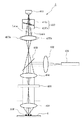
従来のOA検出系を備えた投影露光光学系について、その概略を示す図3の模式図を用いて解説する。
【0010】
露光光源を含む露光照明光学系1(光源としては水銀ランプ、KrFエキシマレーザ、やArFエキシマレーザ等)から出射した光ILは、パターンを形成しているマスク(レチクル)2を照明する。この時レチクル2は、レチクル2上方(或いは下方)に配置されたアライメント検出系11によって投影露光光学系3の光軸AXとレチクルパターンの中心が一致するように、レチクルホルダ12,12' に予め位置決めされている。
【0011】
レチクルパターンを通った光に基づいて、投影露光光学系3により、その像はウエハステージ8上に保持されたウエハ6に所定の倍率で転写される。尚、レチクル2の上方から照射光を照射し、投影露光光学系3を介して、固定位置でレチクルパターンをウエハ6上に順次露光するのがステッパと呼ばれ、レチクル2及びウエハ6が相対的に移動(レチクル2の移動量はウエハ6の移動量に投影倍率を乗じた分)する露光装置をスキャナ(走査型露光装置)と呼ぶ。
【0012】
一方、ウエハ6にはセカンドウエハと呼ばれる既にパターンが形成されている種類のものが有り、このウエハに次のパターンを形成する場合には、予めウエハの位置を検出しておかなければならない。その位置検出方法に上記のTTL−AA方式やOA検出方式がある。
【0013】
ここでは、OA検出系を備えたアライメント方式に関して、図3に基づいて解説する。同図に示すように、OA検出系4は、投影露光光学系3とは別個に構成されており、ウエハステージ8は横方向距離を計測出来る干渉計9に基づいて駆動し、OA検出系4の観察領域にウエハ6を位置決めする。干渉計9に基づいて位置決めされたウエハ6に対して、ウエハ6上に形成されたアライメントマークAMをOA検出系4で位置検出し、ウエハ6上に形成されたチップ(素子)の配列情報を得ることが出来る。
【0014】
次に、このチップ(素子)の配列情報に基づいて、ウエハ6を投影露光光学系3の露光領域(レチクルの転写領域)にウエハステージ8を駆動して、順次露光を行っていく。
【0015】
ここで、通常投影露光光学系3の露光領域には、投影露光光学系3のフォーカス方向を計測するフォーカス検出系5が構成されている。このフォーカス検出系5の構成は、照明光源501から出射した光を照明レンズ502を介してスリットパターン503を照明する。スリットパターン503を透過した光で照明光学系504、ミラー505によってウエハ6上にスリットパターンを結像する。
【0016】
ウエハ6上に投影されたスリットパターンは該ウエハ6の表面上で反射し、照明系と反対側に構成されたミラー506、検出光学系507に入射する。検出光学系507はウエハ6上に形成されたスリット像を光電変換素子508上に再結像させる。ウエハ6が上下することで、光電変換素子508上のスリット像が移動し、その移動量からウエハ6のフォーカス方向の距離を測定出来る。通常は、このスリットを複数(ウエハ6上の多点)用意しておき、それぞれのフォーカス位置を検出すること(ウエハ6上の多点計測)で、投影露光光学系3のレチクル像の像面に対するウエハ6の傾きを計測することも出来る。
【0017】
更にOA検出系4について、図4の概略図を参照しながら解説する。
図4中に於いて、照明光源401(ファイバ等)から導光された光は、照明光学系402により、偏光ビームスプリッタ403に導かれる。偏光ビームスプリッタ403によって反射された紙面に垂直なS偏光光は、リレーレンズ404、λ/4板(四分の一波長板)409を通過した後、円偏光に変換され、対物レンズ405を通ってウエハ6上に形成されたアライメントマークAMをケラー照明する。
【0018】
アライメントマークAMから発生した反射光、回折光、散乱光は、再度対物レンズ405、λ/4板409に戻り、今度は紙面に平行なP偏光に変換され、偏光ビームスプリッタ403を通過し、結像光学系407a(407b)によって、アライメントマークAMの像を光電変換素子411(例えばCCDカメラ)上に形成する。光電変換されたアライメントマーク像の位置に基づいて、ウエハ6の位置を検出する。
【0019】
この時、ウエハ6上のアライメントマークAMを精度良く検出する為には、アライメントマークAMの像が明確に検出されなければならない。つまり、OA検出系4のピントがアライメントマークAMに合っていなければならない。
【0020】
その為に、一般的には不図示のAF検出系が構成されており、その検出結果に基づいて、アライメントマークをOA検出系のベストフォーカス面に駆動して、アライメントマークの検出を行っている。
【0021】
尚、TTL−AA方式についての説明はここでは割愛するが、基本的にはOA検出系を投影光学系3を介して、ウエハ上を観察する構成をしている点が異なっている。
【0022】
【発明が解決しようとする課題】
しかしながら、上記の様なアライメントスコープにより、ウエハ上のマークを観察、位置検出する場合、マーク上部に塗布、或いは形成された透明層の為、単色光では干渉縞が発生してしまう。その為、アライメント信号に干渉縞の信号が加算された状態で検出され、高精度に検出できなくなる。従って、一般的にこうしたアライメントスコープの光源としては、広帯域の波長を持つものが使用され、干渉縞の少ない信号として検出する。
【0023】
ところが、実際製造されるアライメントスコープでは、構成されている光学部品等の製造誤差や組み立て誤差によって、収差が発生している。特に、レンズ等の平行偏心や傾き偏心、他には平行平板(プリズム等)の傾き偏心によって、波長に依存したシフトが発生してしまう。所謂プリズム効果によって、色にじみが発生してしまう。上記の様に、波長を広帯域化したり、投影露光光学系を介したりすることで、この波長毎に発生するシフト(以下この現象によって発生するシフトを「波長シフト」と呼ぶ。)が大きくなる場合がある。
【0024】
図4に戻りこの現象を説明すると、例えば、実線で示す検出光学系407aは光軸に対して、偏心を持たない状態で配置(設計値の位置)されているものとする。一方、破線で示す検出光学系407bは、光軸から若干偏心した状態で配置されたものとする。この様に、光軸に対して偏心するのは製造上の誤差によるものであり、実際のアライメントスコープでは、制御できない量で発生する可能性がある。
【0025】
この様に、レンズが偏心してしまうと、所謂レンズのプリズム効果により、予期せぬ波長シフトが発生してしまう。実線で示す光線Lmaは、設計的な光線を表し、破線で示す光線Lmbはプリズム効果により、波長に依存した量だけずれが発生していることを表している。
【0026】
こうした波長に依存したずれを持つ光学系で、アライメントマークを観察した場合のデメリットを以下に図5及び図6を用いて解説する。
【0027】
図5及び図6中の(a)は、アライメントマークの断面を模式的に表現したものであり、図5(a)は、単純な段差構造を持つマークを表し、図6(a)は、段差構造の上にレジストの様な透明層(図中斜線部)が形成されているマークを表現している。尚、計測方向は、図中のX方向とする。また、図5及び図6の(b)から(d)までは、アライメントスコープで使用している波長を3つとして(第1波長:λ1 、第2波長:λ2 、第3波長:λ3 )、それぞれの波長成分で検出されるアライメントマークの波形を表している。図5及び図6の(e)は、第1波長λ1 から第3波長λ3 までをすべて重ね合わせた波形を示し、この波形が実際にアライメントマークを検出する際の波形を表現している。
【0028】
図5は、上記の波長シフトがないアライメントスコープで検出される場合を表している。波長シフトが存在しない場合、波長λ1 〜λ3 の各波形の中心位置はアライメントマークの中心と一致しており、全ての波長を重ね合わせたλall の波形( 図5(e)) の中心位置も一致する。
【0029】
一方、図6の場合、アライメントスコープに波長シフトが存在している場合であり、波長毎に検出される波形の中心位置がずれてしまう。更に、アライメントマーク上の透明層の為、各波長での信号強度が変化してしまう(例えば、図6(c)に示す波長λ1 の信号強度は、図5(c)に示す波長λ1 の信号強度に対し強度変化ΔI だけ低下する)。その為、全ての波長での合成波形は各波長の中心位置ずれと強度差によって、実際のアライメントマークの中心からずれて(シフト(Shift )して)しまう。この様に、波長シフトがアライメントスコープに存在する場合、本例の様に透明層の厚みによって、各波長の信号強度の重みが変化し、その為、シフト量が変化してしまう恐れがある。
【0030】
こうした波長シフトがある場合に対して、従来では2枚の楔の回転を利用し、楔で発生する波長シフトにより調整する方法がある。図7にその模式図を示す。
波長シフトがX方向に発生している場合、2枚の楔は光軸周りに回転調整される。この様に回転調整すると波長に依存して、シフトΔが発生し、光学系全体で発生した−Δ分だけ補正可能となる。ところが、この様に楔を回転させて調整する場合、Y方向にも楔成分がある為、所望の調整が困難になる。また、元々、平行に光線がセンサ上に入射するべきところが、楔を通ったことにより、光線がθt 分だけ傾いてしまう。この様に、光線が傾いてしまうと、センサの感度が落ちてしまう等の弊害を発生してしまう問題と、アッパ(Upper )光線Lupper とロワー(Lower )光線Llower の透過するガラス部分の厚みが異なってしまい、その結果、フォーカス(Focus )ポイントが画角の上下で異なってしまう。これでは、マーク領域全体に対して、ベストフォーカスに合わせることが出来ず、位置検出精度が劣化してしまう。
【0031】
以上の様な弊害が発生しない方法として、平行平板の傾きを利用して、波長シフトを取る方法が考えられる。図12には、その方法説明用の模式図を示す。
【0032】
この場合、大きな波長シフトを発生させる為には、平行平板30の傾き角θを大きくするか或いは、平行平板30の厚みtを厚くしなくてはならない。実際の装置を考えると、この様にガラスの厚みtを厚くし、傾き角θを大きくすることは、装置自身の拡大化というデメリットを発生する。
【0033】
本発明は、上記の様なアライメントスコープの製造誤差によって発生する波長シフトを補正し、調整して、更には他の収差の発生を極力抑えることの出来る構成を開示するものである。従って、高精度な検出を可能とした検出装置を提供することを目的とするものである。
【0034】
【課題を解決するための手段】
上記目的を達成するために、本発明に係る位置検出装置は、検出対象からの光を光学系を介して受光手段により受光することにより、前記検出対象に関する位置情報を検出する位置検出装置であって、前記光学系の光路内に配置された複数の楔光学部材を有し、前記複数の楔光学部材は、少なくとも一対の平行に対向した楔面を有し、前記対向した楔面は前記光学系の光軸に垂直な面に対し傾いており、該傾いた楔面を持つ前記複数の楔光学部材の楔方向は前記受光手段による計測方向に配置され、前記複数の楔光学部材は、前記対向した楔面の間隔が調整可能であり、前記楔方向が反転可能であることを特徴とする。
【0043】
【発明の実施の形態】
(第1の実施形態)
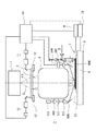
図1には、本発明の第1の実施形態に係るOA検出系について模式的に表す。尚、先の図4の中で記述済みのものについては、同じ符号を付けてある。
ファイバ等の光源401から出射した光は、照明光学系402により、偏光ビームスプリッタ403に導かれる。偏光ビームスプリッタ403によって反射された紙面に垂直なS偏光光は、リレーレンズ404、λ/4板409を通過した後、円偏光に変換され、対物レンズ405を通って感光基板であるウエハ6上に形成された検出対象としてのアライメントマークAMをケラー照明する。
【0044】
検出対象であるアライメントマークAMから発生した反射光、回折光、散乱光は、再度対物レンズ405、λ/4板409に戻り、今度は紙面に平行なP偏光光に変換され、偏光ビームスプリッタ403を通過し、結像光学系407a(407b)によって、アライメントマークAMの像を光電変換素子411(例えばCCDカメラ)上に形成する。即ち、光電変換素子411は、検出対象からの光を光学系を介して受光することにより、検出対象の像を自らの上に形成する。結像光学系407aは設計値上の理想位置は実線で示す位置であるが、実際の組み立て上の誤差によって、若干偏心した破線で示す位置407bにあるとする。その為、上述した波長シフトが発生している。
【0045】
光電変換素子411の直前(検出物体と共役面或いはその近傍)には、楔光学部材群410を構成する2枚の楔光学部材410a,410b(以下この楔光学部材を楔と略称する)が、一対の平行に対向した楔面を有し、かつ、光学系の光軸に垂直な面に対して傾いた状態で配置されている。この2枚の楔の効果等については、以下に示す。
【0046】
光電変換素子411上に結像されたアライメントマークは、電気信号に変換された後、電気的に処理されアライメントマークAMの位置が算出される。
【0047】
算出されたアライメントマーク位置とウエハステージ(不図示)の位置を干渉計に基づいて、ウエハ6上に形成されたショット配列を算出し、露光する。
【0048】
ここで、2枚の楔410a,410bの構成及び作用効果について、図2に基づいて解説する。図2において、2枚の楔20a,20bは隣り合い対向配置した楔面20a2と楔面20b1が平行になるように構成され、光軸と垂直な方向に対してθだけ傾いている。一方、隣り合わず互いに背向する面20a1と面20b2は光軸に対して、垂直になる様に構成されている。2枚の楔20a,20bの内、少なくとも一方は光軸方向に駆動、調整可能であり、アライメントスコープ全体で発生している波長シフトを補正できるようになっている。尚、ここでは、説明を判りやすくする為、各画角の主光線のみを表記した。また、波長シフトを表現しやすくする為に、楔20aまでに到達する光線には、波長シフトが無い状態での表現にしている。又、楔を光軸方向に駆動、調整する機構が存在するが、ここでは図示を省略している。又これは変形例として、アライメントスコープ組み立て時にこの楔を光軸方向に調整し、出荷段階では楔を装置内で固定する構成としてもよい。
【0049】
2枚の楔20a,20bは、像面(或いは、像面と共役な関係)の近傍に配置することが必要である。像面近傍に配置することで、波長シフト量を楔面20a2と楔面20b1の間隔調節によって、補正し、調整することが可能となる。マークの計測方向は図中のX方向とし、X方向に発生している波長シフトを補正する場合について解説する。尚、Y方向に発生している場合は、本楔を光軸周りに90度回転させた配置とすれば良いだけである為、今は説明を割愛する。光線Lm は、アライメントマークの1点からの光線を表している。この光線Lm には、中心波長λ2 とし、短波長λ1 、長波長λ3 なる光線が含まれている。アライメント波長は、λ1 〜λ3 を波長幅とする光を使用していることとする。
【0050】
光線Lm は、楔20aの第1面20a1に垂直に入射し、傾けた楔面である第2面20a2に向かう。ここで、面20a1では、垂直に光線が入射している為、波長λ1 〜λ3 の光はそのまま光路を変えずに直進する。ところが、楔面20a2では、光軸に垂直な面に対しある角度θで傾いている為、各波長に対して屈折角を異ならした角度に向かう。尚、ガラスは波長に対して屈折率が異なっており、各波長(λ1 〜λ3 )に対する屈折率をn1 、n2 、n3 とすると、入射角θに対して所謂スネルの公式に基づいて、n1 ×Sinθ=Sinθλ1 、n2 ×Sinθ=Sinθλ2 、n3 ×Sinθ=Sinθλ3 の関係式が成立する。尚、θλ1 〜θλ3 は、各波長に対する楔面20a2を出射する角度である。2枚の楔20a,20bはある楔面間隔dで配置されており、波長λ1 〜λ3 の光は2枚目の第1面20b1に到達する。その際にθλ1 〜θλ3 が異なる為、間隔dに比例して、楔面20b1のX方向に異なった位置に到達する。楔20aと楔20bは同一の硝材で構成されており、また楔面20a2と楔面20b1は平行に配置されている為、波長λ1 〜λ3 の光線は、楔面20b1で再び光軸に平行な光線に変換される。その後、光軸に平行なまま、波長λ1 〜λ3 の光は波長シフトΔ分だけ持ったまま、光電変換素子411上に到達する。尚、2枚の楔を光軸周りに180度回転することによって、波長シフトを−Δにすることが出来、また0にしたければ間隔dを0にすれば良い。以上の様に、ある波長範囲の光を2枚の楔で且つ隣り合う楔面を平行に配置している場合、その楔の間隔dに比例して、波長シフトを発生させることができる。本説明では、判り易くする為に検出光Lm に波長シフトが無い場合について、解説したが、実際のアライメントスコープに於いては、製造誤差等によって、検出系自体が波長シフトを持ってしまう。そこで、アライメントスコープ自体に波長シフトΔだけ存在している場合は、楔の間隔で発生する波長シフトを−Δになる様に楔の方向及び間隔dを調整すれば良い。以上の様に構成した2枚の楔で波長シフトを補正することは、入射光Lm に対して、出射光が同じ角度のまま光電変換素子に向かう為、従来の様に、非計測方向(Y方向)に発生する波長シフトを考慮する必要がなく、高精度な調整が可能となる。また画角に依存した光、アッパ光線Lupper もロワー光線Llower も光軸光線も同じ光路長のガラス部分を透過する為、画角に依存したフォーカス(Focus )変動が発生しない。
【0051】
尚、2枚の楔20a,20bの楔面間隔dを調整することで、光電変換素子411上の主光線の位置がX方向に変動するが、その変動分は光電変換素子411の中心が画角0に一致するように調整すれば良い。また、楔面の角度θは、そのアライメントスコープで発生しうる波長シフト量と調整間隔dと使用している硝材の分散係数によって最適な角度にすれば良い。出来るだけ、分散係数の大きな硝材を使用することで、楔角θと間隔dを小さくすることが可能である。
【0052】
また、本図に示す場合は、楔を光軸に平行に駆動しているが、厳密に言うと間隔dを変えることで、楔を透過する光路長が若干変化する。この変化量は楔の角度θ及び楔面間隔dに依存している。そこで、その誤差も補正する場合を、図9を用いて解説する。
【0053】
図9に於いては、楔20a,20bを中心波長λ2 の屈折角θλ2 の方向と平行な方向に駆動することで、即ち、楔面で発生する光線の屈折角に平行な方向にその間隔を変化させる機能を有することで、楔面間隔dに依らず、楔中を透過する光路長が変化しない構成が可能となる。尚、波長λ1 、λ3 に対する光路長は変化するが、実際に発生する波長シフト量を考慮すると、その発生量は非常に微少で問題になる量ではない。
【0054】
次に、計測方向が2次元である場合であって、且つ2次元的に波長シフトが発生している場合の波長シフト補正について、図11(a)及び(b)を用いて解説する。
【0055】
図11に於いて、X方向の計測については、図2で解説したように、第1の楔光学部材群を構成する2枚の楔20a,20bを用いて調整する。一方、Y方向については、Y方向に楔面を持つ第2の楔光学部材群を構成する2枚の楔20a,20bを用いて調整する。楔20a,20bは楔21a,21bに対し光軸周りに90度回転した構成とする。
【0056】
図11(a)は、ZX断面から見た図、図11(b)は、YZ断面から見た図を表している。この位置検出系は、上記の様に楔方向に対して、波長シフトが発生する機構にすることが出来る。従って、X方向の波長シフトが発生している場合、楔20a,20bの楔面間隔dx を調整し、Y方向の波長シフトに関しては、2枚の楔21a,21bの楔面間隔dy を調整することで、所望の波長シフト量にXYそれぞれの方向に調整することが可能となる。
【0057】
以上の様に、2組の楔を使って、XY方向それぞれ独立に調整することが出来る為、高精度な調整が可能となることは、説明を要しないであろう。尚、図2で解説したように、アライメントスコープで波長シフトが発生していない場合、間隔dx ,dy は0にすればよく、また、方向を管理したければ、2枚の楔を180度回転すれば良いことも既に解説した通りである。
【0058】
本実施形態によれば、以上の様に、2枚の楔で隣り合う楔面を平行に保ったまま、光軸方向に楔面間隔dを制御することで、アライメントスコープ等に構成されている光学部品の偏心や光学部品の製造誤差で発生した波長シフトを補正し、調整することが可能となり、アライメントマークの波長に依存したシフト量の発生を抑えることができ、高精度なアライメントが可能となる。
【0059】
(第2の実施形態)
次に、本発明の第2の実施形態として、2枚の楔の配置条件について、図10、図13及び図14を用いて解説する。
【0060】
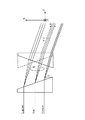
図10は、アライメントスコープ中のある像面Img(アライメントマークと共役面)近傍に2枚の楔を配置した時の模式図を表している。第1の実施形態では、解説を簡略化する為に、光線を主光線だけで表現した場合で説明した。ところが、実際のアライメントスコープでは、ある広がりを持った光束(あるNAを持った光束)として、アライメントマークは結像される。ある画角の光線(本図は、中心波長λ2 だけに着目している)は主光線Priと角度+NAを持った光線L+na と角度−NAを持った光線L-na によって像を結像している。尚、本図の符号は上記第1の実施形態において既に説明したものに対して、同じ符号を付けている。2枚の楔20a,20bを透過する場合、光線L+na と光線L-na では、楔面に入射する角度が異なる為、像面Img上で交差する点が主光線Priに対してずれてしまう。このずれが、所謂軸上コマ収差とも言われ、この収差があることでアライメント計測誤差を生む要因となる。従って、出来るだけこの様な収差の発生を抑えつつ、波長シフトを調整し、補正することが非常に重要である。
【0061】
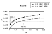
そこで、このNA、楔で発生するコマ収差、楔間隔の量について調べた。
図13は、図10に示すNAと楔面間隔dと発生するコマ収差量(CM)について、グラフ化した図である。横軸はNAであり、縦軸は発生するコマ収差(CM)を対数として示している。尚、楔の角度θは20度とし、楔の屈折率は1.8として計算している。また、実線は対向する楔面間隔dが10mmの場合であり、破線は楔面間隔dが1mmの場合を示している。
【0062】
このグラフからも分かるように、NAが大きくなるに従って、コマ収差量CMが急激に大きくなることが分かる。
【0063】
ここで、ある物体(アライメントマーク)を拡大系のアライメントスコープで検出した場合を考える。この結像倍率は、物体から検出器(光電変換素子等)まで−10倍とする。また、物体上でのNAは0.1とすると、光電変換素子上でのNAは結像倍率分小さくなり0.01となる。
【0064】
結像倍率が−10倍と言うことは、像面側Img(光電変換素子側)で発生する波長シフト量は、物体側で発生する波長シフトの10倍となる。つまり、像面側で発生する波長シフト量を1/10倍すると物体側での発生量に変換できる。また、波長シフト量と楔の間隔の関係は比例関係の為、同じ波長シフト量を物体側で取る場合の楔間隔は、像面側での楔間隔の1/10になる。また、発生したコマ収差の関係は、像面側で発生する量を1/10倍すると物体側での同じ量に相当する。
【0065】
図13に戻り、ある波長シフト量を物体側で取る場合と、同じ波長シフト量を像面側で取る場合について、まとめて見ると、表1のとおりとなる。
【0066】
【表1】

以上の結果から分かる様に、同じ楔角の楔を使って、同じ波長シフト量の補正を考えた場合、NAが小さいところに構成した方が、コマ収差の発生を抑えることが出来る。つまり、本実施形態における2枚の楔での波長シフトを補正する場合、出来るだけNAの小さいところ、言い換えると結像倍率の高いところに構成することで、楔で発生するコマ収差量を抑えることが出来るのが分かる。
【0068】
また、別の条件から表したものが、図14である。本図は、同じ波長シフト量に対して、楔面間隔を一定にし、楔の角度を変えた場合について、グラフ化したものである。楔角に付いては、Sinθの関数で波長シフトが発生する為、角度θの比例で波長シフトが変わる訳ではない。楔角20度の楔に対し発生する波長シフト量の1/10を楔角で取る場合、約3.5度の楔が必要になる。但し、楔面間隔dは、共に10mmとする。
【0069】
この場合も、NAに依存して、発生するコマ収差量が急激に大きくなることが分かる。
【0070】
そこで、上記と同様に、同じ波長シフト量を同じ楔面間隔で、物体面側と像面側で取った場合の発生量に付いて、読み取って見ると表2のようになる。
【0071】
【表2】
以上より、明らかな様に楔角を変更しても、NAが小さいところで調整した方が、コマ収差の発生を抑えることが出来ることは明白である。従って、楔角を最適化し、楔間隔を一定にした場合でも、出来るだけ結像倍率の高いところ(NAの小さいところ)の像面(或いは像面と共役な位置)或いはその近傍に2枚の楔を構成することが、コマ収差の抑制になることが分かる。尚、楔の厚み及び、配置される場所(光線L+na と光線L-na の間隔)には、コマ収差の発生量は依存していない。コマ収差は、NAと楔面間隔dと楔角に依存している。
【0073】
尚、上記では楔が発生するコマ収差と言う観点から、NAの低いところ(結像倍率の大きいところ)に構成することが、有利として来たが、実際製造する楔の精度と言う観点からも、同じことが言える。つまり、2枚の楔の角度θに依存して、コマ収差が発生し、また波長シフトも発生する為、結像倍率の低いところでは、楔の角度誤差が、予期せぬ波長シフト、及びコマ収差を発生してしまう。また、結像倍率の低いところに構成すると間隔の敏感度も高くなる為、調整難易度も上がってしまうと言うデメリットを持つ。従って、調整難易度、楔部品の製造精度と言う観点からも結像倍率の高いところに配置するのが良いと言える。
【0074】
(第3の実施形態)
以上の様に2枚の楔の間隔で波長シフトを調整する場合の更に最適なアライメントスコープの形態について、本発明の第3の実施形態として解説する。図15及び図16には結像光学系407の所謂両側テレセントリックな光学系と、像面側が片側テレセントリックな光学系の2タイプで表現している。これらの系に対して、2枚の楔を構成した場合の特徴について解説する。図15に示す様なテレセントリックな光線に対して、楔を構成した場合は、第1の実施形態(図2)で説明したように、全ての画角に対して、楔を透過する光路長が等しくなり、画角に対するフォーカス(Focus )変動は無い。また、各像高で発生する波長シフト量も同一となり、検出画角全体に渡り良好に補正、調整が可能となる。
【0075】
一方、図16に示すような非テレセントリックな光束に対して、2枚の楔を構成した場合、画角に対して同一の波長シフトを発生させることが困難になる。その詳細図を図8に表す。
【0076】
第1の実施形態(図2)で解説したように分かり易くする為に、図8に於いても主光線だけで表現しており、アライメントスコープ全体としては、波長シフトが発生していないものとして表現している。高い画角のアッパ光線Lupper と低い画角のロワー光線Llower との2つの光線を表した。アッパ光線Lupper は、第1楔20aの第1面20a1である傾いた角度θi にて入射する。その為、第1面20a1でも波長シフトが発生して、その後第2面20a2に向かう。ここで、短波長の光をλ1 (破線)とし、中心波長の光をλ2 (実線)、長波長の光をλ3 (一点鎖線)として表した。第2面20a2では更に屈折が発生し、波長に依存した角度で第2楔の第1面20b1に向かう。更に、面20b1で屈折をした後、面20b2に向かい、再度そこで屈折して、入射した側と同じ角度で光電変換素子411に向かう。この時、中心波長λ2 に対して、発生する波長シフト量をそれぞれの波長に対して、Δλ1u、とΔλ3uと表現している。
【0077】
一方、ロワー光線Llower は、同様に−θi の角度で楔に入射する。第1楔20aの第1面20a1では、上記の様に波長毎に屈折角が異なり、第2面20b2に向かう。ここで、第1面20b1に対して、アッパ光線Lupper とロワー光線Llower では、屈折する方向が異なっており、且つ第2面20a2までの距離が異なっている。また、第2面20a2での屈折では、光線Lupper と異なった角度で各波長は出射される。その為、結果として、第2楔の第1面20b1までの光路長が異なり、発生する波長シフト量が異なってしまう。その結果、光電変換素子411上での波長シフトが中心波長に対して、Δλ1lとΔλ3lだけ発生する。上記のΔλ1uとΔλ1l、及びΔλ3uとΔλ3lでは、発生する方向が異なり、且つ発生量の絶対値も異なってしまう。尚、発生する方向が異なる現象は、楔の角度、入射角θi に依存しており、必ずしも方向が異なるとは限らない。但し、発生する量については、画角の高い光線と低い光線では、異なってしまう。
【0078】
以上の様に、非テレセントリックな場所に2枚の楔を構成し、波長シフトを調整する場合、全ての画角に対して、一様に補正することが困難になる。従って、テレセントリックな光学系で、且つ第2の実施形態で示すようなNAの小さな像面(或いは共役面)に2枚の楔を構成することで、コマ収差の発生を抑え、且つ検出画角に一様に補正することが出来る。尚、非テレセントリックな光学系に2枚の楔を構成すると、波長に依存したコマ収差も発生する。そうした観点からも、極力テレセントリックな場所に、2枚の楔を配置しその間隔調整で、波長シフトを調整することに効果があることが分かる。
【0079】
(第4の実施形態)
以上の実施形態では、OA検出系について述べてきたが、本発明の第4の実施形態では、投影露光光学系を通して、ウエハ上のアライメントマークを観察するTTL−AAについて、図17を参照しながら解説する。尚、図1の中で説明し、同じ機能を有する部材に対しては、図17において図1と同一の符号を付けてある。
【0080】
ファイバ等の光源401からは、ある波長幅を持ち、露光光とは異なる波長(所謂非露光光)が出射し、照明レンズ402に向かう。その後、偏光ビームスプリッタ403に入射し、紙面に垂直なS偏光成分の光がリレーレンズ404、λ/4板409及び対物レンズ405に導光される。その後、ミラー412で反射した光は、投影露光光学系3を通して、ウエハ6上に形成されたアライメントマークAMをケラー照明する。アライメントマークAMからの反射、散乱、回折光は再び、投影露光光学系3を逆に戻り、対物レンズ405、リレーレンズ404を介して、検出レンズ側に導光される。尚、対物レンズ405は、投影露光光学系3で発生する色収差等を補正するように、構成されている。
【0081】
λ/4板409を透過した光は、その偏光面を90度回転させ、偏光ビームスプリッタ403にP偏光成分として、これを通過する。通過した光は、一旦、中間像面に像を形成し、再度検出光学系により、所望の結像倍率になるように光電変換素子411上に、アライメントマークの像を結像している。光電変換素子411から検出された電気信号に基づいて、位置検出を行う点は、既に上述したOA検出系と同様である。
【0082】
尚、光電変換素子411の手前には、上述した2枚の楔からなる楔光学部材群410が構成されている。本アライメントスコープのように、大きな色収差を発生する投影露光光学系3の様なものを通して構成する場合、波長シフトが発生し易い。その為、実際のアライメントスコープ組み立て上では、楔光学部材群410を構成している2枚の楔の間隔を調整して、所望の波長シフト以内になるように追い込まれ、調整される。尚、この様なTTL−AAでは、一般的に、一方向の計測として構成されている。つまり、本図に於いては、このスコープはY方向の計測のみを行うのが、一般的な構成である。従って、このアライメントスコープには、楔は2枚だけで良く、それと直交する方向の2枚の楔は不要となる。勿論、不図示のX計測用のアライメントスコープには、同様に2枚の楔が構成されており、その方向にのみ最適なる様、楔の間隔調整がなされる。以上の様に、2枚の楔を構成することで、従来からあるTTL−AA系に於いて、投影露光光学系等で発生する波長シフトを補正し、調整することが出来る。従って、波長に依存したシフトの発生を抑えることが出来、高精度な位置検出系を構成できる。
【0083】
また、上述した第1の実施形態〜第4の実施形態については、所謂アライメントスコープに関して、説明して来たが、本発明はこれに限定されるものではない。例えば、投影露光装置に使われているAF検出系(図3記載のフォーカス検出系5)などにも適用できる。
【0084】
AF検出系の場合も、測定対象物からの光を検出し、その光の位置を光電変換素子で検出する。一般にAF検出系5でも、ある波長幅を持った光が利用されており、検出系内に構成している光学部材の製造誤差によって、波長シフトが存在する。AF検出系5の場合も波長シフトが存在すると、ウエハ上の薄膜干渉の為、波長分布特性が変化し、その為検出誤差を発生してしまう。従って、アライメントスコープに限定されず、そうしたAF系にも上述した構成をすることでフォーカス検出系の誤差を軽減することが出来る。
【0085】
また更に、上述の複数の実施形態では、結像回数は2回である場合を例に説明したが、本発明はこれに限定されるものではないことは、言うに及ばない。また本発明の本質は、結像倍率が高く(NAの小さい)、検出物体と共役な面或いは、その近傍に2枚の楔を配置し、その間隔調節で波長シフトを調整するところにある。従って、この本質を逸脱しない範囲に於いては、別の検出形態(例えば、画像検出ではなく光量検出或いは位相検出など)でも適用出来る。
【0086】
(第5の実施形態)
上述までの実施形態では、2枚の楔を使って、一計測方向の波長シフトを補正する場合について、解説してきたが、本発明の第5の実施形態として、3枚の楔を使った場合について、図18を用いて解説する。図18に示す楔光学部材群は、楔面20a2を有する第1楔20aと、第2楔20bと、楔面20c1を有する第3楔20cとによって構成されている。第1楔20aと第3楔20cとの間に配置された中間楔光学部材である第2楔20bは、互いに交差する方向に傾けた2つの楔面20b1,20b2を備えている。
【0087】
楔面で発生する各波長に対する屈折角の違いにより、波長シフトを発生させている点に関しては、上記と同様である為、詳細は割愛する。図18(a)は、3枚の楔の内、第1楔20aの第2面20a2と、第2楔20bの第1面20b1が光軸に対して、所定の角度で傾いて且つ互いに平行になるように配置されている状態を示す。また、第2楔20bの第2面20b2と第3楔20cの第1面20c1面も光軸に対して、所定の角度で傾き且つ互いに平行になり、更に、第2楔20bの第1面20b1とは光軸に対して、傾き方向を異ならせて互いに交差する方向に傾けた構成になっている。
【0088】
図18に於いては、分かり易くする為に楔角θ1とθ2の絶対値は同じで符号を異ならしている。また、第1楔20aから第3楔20cまで全て同じ硝材(屈折率)のものを使っているとする。
【0089】
図18(a)に於いて、θ1 =−θ2 と言う関係及び、第1楔20aと第2楔20bの間隔d1 と第2楔20bと第3楔20cの間隔d2 が等しく(d1 =d2 =d)なるように配置されている場合、各楔面で波長毎に屈折角が異なって伝播するが、第1楔20aと第2楔20b間の波長シフトと、第2楔20bと第3楔20cとの間の波長シフトでキャンセルされ、結果として楔全体を透過して来た光束は波長シフトを持たない。次に図18(b)に示す様に、第2楔20bを第1楔20aに当接するまで移動させた場合を考える(d1 =0、d2 =2d)。この場合、第1楔20aと第2楔20b間では、波長シフトは発生せず、第2楔20bと第3楔20c間でのみ波長シフトが発生する。逆に図18(c)に示すように、第2楔20bを第3楔20cまで移動させると(d1 =2d、d2 =0)、今度は第1楔20aと第2楔20bの間で波長シフトが発生する。そこで、図18の(b)と(c)を比べて見ると、第2楔20bの第1面20b1と第2面20b2の楔角が逆になっている為に、(b) から(c)までに移動する間に、波長シフトの方向が逆転することが分かる。つまり、アライメントスコープ自体に波長シフトが存在しない場合、図18(a)に示すように、第2楔20bを中間の位置に配置し、図18(b)で発生する波長シフトを正と定義すると、アライメントスコープが負の波長シフトを持っている場合、図18(b)の位置の方向に第2楔20bを調整し、逆にアライメントスコープが正の波長シフトを持つ場合、図18(c)の方向に、第2楔20bを調整すれば良い。以上の様な3枚の楔を使うことで、上述して来た2枚の楔を使う構成に比べ、楔全体を180度回転せずとも、符号を反転した波長シフト調整が可能となる。
【0090】
尚、本実施形態では分かり易くする為に、第2楔20bの第1面20b1と第2面20b2の楔角を絶対値が等しく符号の異なる角としたが、これに限定されるものではない。つまり、θ1 ≠−θ2 の場合、d1 ≠d2 となる位置で、波長シフトが0になり、第2楔20bの移動に対する波長シフト発生量の敏感度が異なってくるだけである。
【0091】
また、上述してきた第1の実施形態〜第4の実施形態の全てに対して、この第5の実施形態の適用は可能であることは明白である。また、本実施形態では、3枚の楔を使った例を述べたが、枚数に関してはこれに限定されない。更に4枚以上の構成でも同じ効果、調整は可能である。
【0092】
以上の様に、3枚の楔を使って、楔間隔の調整だけで符号も含めて波長シフトを調整することが出来、アライメントスコープ等が持っている製造誤差等で発生した波長シフトを補正し、調整することが可能となる。その為、高精度な位置検出可能な検出装置或いは該検出装置を用いた投影露光装置を提供することが出来る。
【0093】
(半導体生産システムの実施形態)
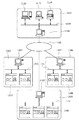
次に、本発明に係る装置を用いた半導体デバイス(ICやLSI等の半導体チップ、液晶パネル、CCD、薄膜磁気ヘッド、マイクロマシン等)の生産システムの例を説明する。これは半導体製造工場に設置された製造装置のトラブル対応や定期メンテナンス、あるいはソフトウェア提供などの保守サービスを、製造工場外のコンピュータネットワークを利用して行うものである。
【0094】
図19は全体システムをある角度から切り出して表現したものである。図中、1101は半導体デバイスの製造装置を提供するベンダ(装置供給メーカ)の事業所である。製造装置の実例としては、半導体製造工場で使用する各種プロセス用の半導体製造装置、例えば、前工程用機器(露光装置、レジスト処理装置、エッチング装置等のリソグラフィ装置、熱処理装置、成膜装置、平坦化装置等)や後工程用機器(組立て装置、検査装置等)を想定している。事業所1101内には、製造装置の保守データベースを提供するホスト管理システム1108、複数の操作端末コンピュータ1110、これらを結んでイントラネット等を構築するローカルエリアネットワーク(LAN)1109を備える。ホスト管理システム1108は、LAN1109を事業所の外部ネットワークであるインターネット1105に接続するためのゲートウェイと、外部からのアクセスを制限するセキュリティ機能を備える。
【0095】
一方、1102〜1104は、製造装置のユーザとしての半導体製造メーカの製造工場である。製造工場1102〜1104は、互いに異なるメーカに属する工場であっても良いし、同一のメーカに属する工場(例えば、前工程用の工場、後工程用の工場等)であっても良い。各工場1102〜1104内には、夫々、複数の製造装置1106と、それらを結んでイントラネット等を構築するローカルエリアネットワーク(LAN)1111と、各製造装置1106の稼動状況を監視する監視装置としてホスト管理システム1107とが設けられている。各工場1102〜1104に設けられたホスト管理システム1107は、各工場内のLAN1111を工場の外部ネットワークであるインターネット1105に接続するためのゲートウェイを備える。これにより各工場のLAN1111からインターネット1105を介してベンダ1101側のホスト管理システム1108にアクセスが可能となり、ホスト管理システム1108のセキュリティ機能によって限られたユーザだけにアクセスが許可となっている。具体的には、インターネット1105を介して、各製造装置1106の稼動状況を示すステータス情報(例えば、トラブルが発生した製造装置の症状)を工場側からベンダ側に通知する他、その通知に対応する応答情報(例えば、トラブルに対する対処方法を指示する情報、対処用のソフトウェアやデータ)や、最新のソフトウェア、ヘルプ情報などの保守情報をベンダ側から受け取ることができる。本発明に関連していえば、例えば、楔間の距離dあるいはこれに起因して補正されるべき波長依存の検出ずれのデータが各露光装置からホスト管理システム1107によってインターネット1105を介してベンダ1101側のホスト管理システム1108に送信し、ベンダ側で各装置別の保守情報管理、全装置にわたる統計処理等を行ない、又これらによってベンダ側で作成された補正プログラム情報、保守情報、ヘルプ情報を各装置別にインターネット1105を介して該当するホスト管理システム1107に送信する。各工場1102〜1104とベンダ1101との間のデータ通信および各工場内のLAN1111でのデータ通信には、インターネットで一般的に使用されている通信プロトコル(TCP/IP)が使用される。なお、工場外の外部ネットワークとしてインターネットを利用する代わりに、第三者からのアクセスができずにセキュリティの高い専用線ネットワーク(ISDNなど)を利用することもできる。また、ホスト管理システムはベンダが提供するものに限らずユーザがデータベースを構築して外部ネットワーク上に置き、ユーザの複数の工場から該データベースへのアクセスを許可するようにしてもよい。
【0096】
さて、図20は本実施形態の全体システムを図19とは別の角度から切り出して表現した概念図である。先の例ではそれぞれが製造装置を備えた複数のユーザ工場と、該製造装置のベンダの管理システムとを外部ネットワークで接続して、該外部ネットワークを介して各工場の生産管理や少なくとも1台の製造装置の情報をデータ通信するものであった。これに対し本例は、複数のベンダの製造装置を備えた工場と、該複数の製造装置のそれぞれのベンダの管理システムとを工場外の外部ネットワークで接続して、各製造装置の保守情報をデータ通信するものである。図中、1201は製造装置ユーザ(半導体デバイス製造メーカ)の製造工場であり、工場の製造ラインには各種プロセスを行う製造装置、ここでは例として露光装置1202、レジスト処理装置1203、成膜処理装置1204が導入されている。なお図20では製造工場1201は1つだけ描いているが、実際は複数の工場が同様にネットワーク化されている。工場内の各装置はLAN1206で接続されてイントラネットを構成し、ホスト管理システム1205で製造ラインの稼動管理がされている。
【0097】
一方、露光装置メーカ1210、レジスト処理装置メーカ1220、成膜装置メーカ1230などベンダ(装置供給メーカ)の各事業所には、それぞれ供給した機器の遠隔保守を行うためのホスト管理システム1211,1221,1231を備え、これらは上述したように保守データベースと外部ネットワークのゲートウェイを備える。ユーザの製造工場内の各装置を管理するホスト管理システム1205と、各装置のベンダの管理システム1211,1221,1231とは、外部ネットワーク1200であるインターネットもしくは専用線ネットワークによって接続されている。このシステムにおいて、製造ラインの一連の製造機器の中のどれかにトラブルが起きると、製造ラインの稼動が休止してしまうが、トラブルが起きた機器のベンダからインターネット1200を介した遠隔保守を受けることで迅速な対応が可能であり、製造ラインの休止を最小限に抑えることができる。
【0098】
半導体製造工場に設置された各製造装置はそれぞれ、ディスプレイと、ネットワークインタフェースと、記憶装置にストアされたネットワークアクセス用ソフトウェアならびに装置動作用のソフトウェアを実行するコンピュータを備える。記憶装置としては内蔵メモリやハードディスク、あるいはネットワークファイルサーバーなどである。上記ネットワークアクセス用ソフトウェアは、専用又は汎用のウェブブラウザを含み、例えば図21に一例を示す様な画面のユーザインタフェースをディスプレイ上に提供する。各工場で製造装置を管理するオペレータは、画面を参照しながら、製造装置の機種1401、シリアルナンバー1402、トラブルの件名1403、発生日1404、緊急度1405、症状1406、対処法1407、経過1408等の情報を画面上の入力項目に入力する。入力された情報はインターネットを介して保守データベースに送信され、その結果の適切な保守情報が保守データベースから返信されディスプレイ上に提示される。またウェブブラウザが提供するユーザインタフェースはさらに図示のごとくハイパーリンク機能1410〜1412を実現し、オペレータは各項目の更に詳細な情報にアクセスしたり、ベンダが提供するソフトウェアライブラリから製造装置に使用する最新バージョンのソフトウェアを引出したり、工場のオペレータの参考に供する操作ガイド(ヘルプ情報)を引出したりすることができる。ここで、保守データベースが提供する保守情報には、上記説明した本発明に関する情報も含まれ、また前記ソフトウェアライブラリは本発明を実現するための最新のソフトウェアも提供する。具体的には例えば、前述したような形で、楔間の距離dあるいはこれに起因して補正されるべき波長依存の検出ずれのデータが送信され、これに応じた補正プログラム情報、保守情報等が返信される。
【0099】
次に上記説明した生産システムを利用した半導体デバイスの製造プロセスを説明する。図22は半導体デバイスの全体的な製造プロセスのフローを示す。ステップ1(回路設計)では半導体デバイスの回路設計を行う。ステップ2(マスク製作)では設計した回路パターンを形成したマスクを製作する。一方、ステップ3(ウエハ製造)ではシリコン等の材料を用いてウエハを製造する。ステップ4(ウエハプロセス)は前工程と呼ばれ、上記用意したマスクとウエハを用いて、リソグラフィ技術によってウエハ上に実際の回路を形成する。次のステップ5(組み立て)は後工程と呼ばれ、ステップ4によって作製されたウエハを用いて半導体チップ化する工程であり、アッセンブリ工程(ダイシング、ボンディング)、パッケージング工程(チップ封入)等の組立て工程を含む。ステップ6(検査)ではステップ5で作製された半導体デバイスの動作確認テスト、耐久性テスト等の検査を行う。こうした工程を経て半導体デバイスが完成し、これを出荷(ステップ7)する。前工程と後工程はそれぞれ専用の別の工場で行い、これらの工場毎に上記説明した遠隔保守システムによって保守がなされる。また前工程工場と後工程工場との間でも、インターネットまたは専用線ネットワークを介して生産管理や装置保守のための情報がデータ通信される。
【0100】
図23は上記ウエハプロセスの詳細なフローを示す。ステップ11(酸化)ではウエハの表面を酸化させる。ステップ12(CVD)ではウエハ表面に絶縁膜を成膜する。ステップ13(電極形成)ではウエハ上に電極を蒸着によって形成する。ステップ14(イオン打込み)ではウエハにイオンを打ち込む。ステップ15(レジスト処理)ではウエハに感光剤を塗布する。ステップ16(露光)では上記説明した投影露光装置によってマスクの回路パターンをウエハに焼付露光する。ステップ17(現像)では露光したウエハを現像する。ステップ18(エッチング)では現像したレジスト像以外の部分を削り取る。ステップ19(レジスト剥離)ではエッチングが済んで不要となったレジストを取り除く。これらのステップを繰り返し行うことによって、ウエハ上に多重に回路パターンを形成する。各工程で使用する製造機器は上記説明した遠隔保守システムによって保守がなされているので、トラブルを未然に防ぐと共に、もしトラブルが発生しても迅速な復旧が可能であり、従来に比べて半導体デバイスの生産性を向上させることができる。
【0101】
【発明の効果】
本発明は上述のように、アライメントスコープ等の製造誤差、プリズムの傾き偏心や、レンズ等の偏心、或いは平行平板等の面精度誤差等で発生する波長に依存したシフト(ずれ)を、少なくとも2枚の楔で隣り合う2つの楔面を平行に構成し、楔の楔面間隔をもって調整することが出来る。従って、検出系で発生する波長シフトを高精度に補正し、調整することが出来る。その為、アライメントマーク上にあるレジスト等の透明層の干渉によって、発生する波長シフトを抑えることが出来、高精度な検出装置を提供出来る。また、検出装置中の結像倍率の高いところに楔を構成することで、少なくとも2枚の楔で発生するコマ収差量を少なくすることが出来る。更には、テレセントリックな場所に構成することで、画角全体に渡り良好な波長シフトの補正が可能となる。また、従来のTTL−AAにも適用でき、投影露光光学系で発生する波長シフトも補正、調整が可能となり、高精度な検出装置及び該装置を用いた投影露光装置を提供出来る。また、物体の高さ位置を測定する所謂AF検出系にも同様の構成が適用でき、これらAF検出系の計測精度の向上が期待出来る。
【図面の簡単な説明】
【図1】 本発明の第1の実施形態に係る位置検出系の全体図である。
【図2】 本発明の第1の実施形態に係る2枚の楔で発生する波長シフトを説明するための詳細図である。
【図3】 投影露光光学系を示す模式図である。
【図4】 従来のOA検出系の概略説明用の模式図である。
【図5】 理想的な検出系でのアライメントマークと検出波形の関係を示す図である。
【図6】 波長シフトのある検出系でのアライメントマークと検出波形の関係を示す図である。
【図7】 従来の楔を使った波長シフト補正説明用の模式図である。
【図8】 非テレセントリック系での楔を取る光線の波長シフト説明用の模式図である。
【図9】 本発明の第1の実施形態に係る位置検出系のより高精度な場合の模式図である
【図10】 NAと楔面間隔dと発生するコマ収差量CMを表す模式図である。
【図11】 本発明の第1の実施形態に係る位置検出系によって2次元的に波長シフトを補正する場合の模式図である。
【図12】 別な従来の楔を使った波長シフト補正の模式図である。
【図13】 本発明の第2の実施形態の説明用であって、ある条件でNAと楔で発生するコマ収差のグラフである。
【図14】 本発明の第2の実施形態の説明用であって、別の条件でNAと楔で発生するコマ収差のグラフである。
【図15】 本発明の第3の実施形態に係る両側テレセントリックトリックな光学系の模式図である。
【図16】 片側テレセントリックトリックな光学系の模式図である。
【図17】 本発明の第4の実施形態に係るTTL−AAでの位置検出系を示す模式図である。
【図18】 3枚の楔を使った本発明の第5の実施形態に係る位置検出系を示す模式図である。
【図19】 本発明に係る装置を用いた半導体デバイスの生産システムをある角度から見た概念図である。
【図20】 本発明に係る装置を用いた半導体デバイスの生産システムを別の角度から見た概念図である。
【図21】 ユーザインタフェースの具体例である。
【図22】 デバイスの製造プロセスのフローを説明する図である。
【図23】 ウエハプロセスを説明する図である。
【符号の説明】
1:投影露光照明系、2:レチクル、3:投影露光光学系、4:OA検出系、5:AF検出系(フォーカス検出系)、6:ウエハ、7:干渉計ミラー、8:ウエハステージ、9:干渉計、10:ステージ制御部、11:レチクルアライメント検出系、12, 12’:レチクルホルダ、13:基準マーク、14:制御部、401:アライメント光源、402:照明光学系、403:偏光ビームスプリッタ、404:リレーレンズ、405:対物レンズ、407:検出光学系、409:λ/4(四分の一波長)板、410:楔光学部材群、410a,410b:波長シフト補正楔(楔光学部材)、411:光電変換素子(検出面)、20a,20b, 20c:波長シフト補正楔(楔光学部材)、30:平行平板、1101:ベンダの事業所、1102,1103,1104:製造工場、1105:インターネット、1106:製造装置、1107:工場のホスト管理システム、1108:ベンダ側のホスト管理システム、1109:ベンダ側のローカルエリアネットワーク(LAN)、1110:操作端末コンピュータ、1111:工場のローカルエリアネットワーク(LAN)、1200:外部ネットワーク、1201:製造装置ユーザの製造工場、1202:露光装置、1203:レジスト処理装置、1204:成膜処理装置、1205:工場のホスト管理システム、1206:工場のローカルエリアネットワーク(LAN)、1210:露光装置メーカ、1211:露光装置メーカの事業所のホスト管理システム、1220:レジスト処理装置メーカ、1221:レジスト処理装置メーカの事業所のホスト管理システム、1230:成膜装置メーカ、1231:成膜装置メーカの事業所のホスト管理システム、1401:製造装置の機種、1402:シリアルナンバー、1403:トラブルの件名、1404:発生日、1405:緊急度、1406:症状、1407:対処法、1408:経過、1410,1411,1412:ハイパーリンク機能。[0001]
BACKGROUND OF THE INVENTION
The present invention relates to a detection apparatus that can detect the position of an object to be detected with high accuracy. The present invention also relates to a device manufacturing method using a detection apparatus that guarantees high-precision detection, and in particular, a wafer such as a projection exposure apparatus that manufactures various devices such as semiconductor ICs, LSIs, CCDs, liquid crystal panels, magnetic heads, etc. This is suitable when the position of the object is detected with high accuracy by observing an image on the object and the position of the object is aligned based on the detection information.
[0002]
[Prior art]
In recent years, the progress of semiconductor device manufacturing technology has been remarkable, and the progress of microfabrication technology has been remarkable. In particular, optical processing technology is mainly reduced projection exposure equipment with submicron resolution, commonly known as steppers. To further improve resolution, the numerical aperture (NA) of the optical system is increased and the exposure wavelength is shortened. It has been.
[0003]
Along with the shortening of the exposure wavelength, the exposure light source has also been changed from a g-line or i-line high-pressure mercury lamp to an KrF or ArF excimer laser.
[0004]
On the other hand, with the improvement of the resolution of the projection pattern, high precision is also required for the alignment for relative alignment of the wafer and the mask (reticle) in the projection exposure apparatus. A projection exposure apparatus is not only a high-resolution exposure apparatus but also a function as a highly accurate position detection apparatus.
[0005]
For this reason, the performance of a position detection device for detecting an alignment mark formed on a wafer or the like, that is, a so-called alignment scope itself is required to be highly accurate.
[0006]
Two types of alignment scopes have been proposed and used. One is a so-called off-axis alignment detection system (Off-Axis AA, hereinafter abbreviated as “OA”) that is configured separately without using a projection exposure optical system and optically detects alignment marks.
[0007]
Another conventional configuration, particularly as an alignment method in an i-line exposure apparatus, is performed on a wafer using an alignment wavelength of non-exposure light via a projection light optical system called TTL-AA (Through the Lens Auto Alignment). There is a method for detecting an alignment mark.
[0008]
In any alignment scope, since the aberration of the alignment scope itself generates a position detection error, it is required to reduce the aberration as much as possible or correct the generated aberration.
[0009]
A projection exposure optical system equipped with a conventional OA detection system will be described with reference to the schematic diagram of FIG.
[0010]
Light IL emitted from an exposure illumination
[0011]
Based on the light passing through the reticle pattern, the projection exposure
[0012]
On the other hand, the
[0013]
Here, an alignment method including an OA detection system will be described with reference to FIG. As shown in the figure, the
[0014]
Next, based on the arrangement information of the chips (elements), the
[0015]
Here, a
[0016]
The slit pattern projected on the
[0017]
Further, the
In FIG. 4, the light guided from the illumination light source 401 (fiber or the like) is guided to the
[0018]
Reflected light, diffracted light, and scattered light generated from the alignment mark AM are returned to the
[0019]
At this time, in order to accurately detect the alignment mark AM on the
[0020]
For this purpose, an AF detection system (not shown) is generally configured, and the alignment mark is detected by driving the alignment mark to the best focus surface of the OA detection system based on the detection result. .
[0021]
Although the description of the TTL-AA method is omitted here, the difference is that the OA detection system is basically configured to observe the wafer via the projection
[0022]
[Problems to be solved by the invention]
However, when the mark on the wafer is observed and detected by the alignment scope as described above, interference fringes are generated in the monochromatic light due to the transparent layer applied or formed on the mark. For this reason, detection is performed in a state in which interference fringe signals are added to the alignment signal, and detection with high accuracy becomes impossible. Therefore, in general, a light source having such a broad wavelength is used as the light source of such an alignment scope, and the light is detected as a signal with less interference fringes.
[0023]
However, in an actually manufactured alignment scope, aberration is generated due to a manufacturing error or an assembly error of a configured optical component or the like. In particular, a wavelength-dependent shift occurs due to parallel decentering and tilt decentering of the lens, etc., and other tilt decentering of a parallel plate (prism or the like). Color blurring occurs due to the so-called prism effect. As described above, when the wavelength is broadened or the projection exposure optical system is used, the shift generated for each wavelength (hereinafter, the shift generated by this phenomenon is referred to as “wavelength shift”) becomes large. There is.
[0024]
Returning to FIG. 4, this phenomenon will be described. For example, it is assumed that the detection
[0025]
Thus, when the lens is decentered, an unexpected wavelength shift occurs due to the so-called prism effect of the lens. A light ray Lma indicated by a solid line indicates a design light ray, and a light ray Lmb indicated by a broken line indicates that a shift is generated by an amount depending on the wavelength due to the prism effect.
[0026]
The disadvantages of observing the alignment mark in an optical system having such a wavelength-dependent shift will be described below with reference to FIGS.
[0027]
(A) in FIG. 5 and FIG. 6 schematically represents a cross section of the alignment mark, FIG. 5 (a) represents a mark having a simple step structure, and FIG. It represents a mark in which a transparent layer (shaded portion in the figure) such as a resist is formed on the step structure. The measurement direction is the X direction in the figure. In FIGS. 5 and 6 (b) to (d), three wavelengths used in the alignment scope are assumed (first wavelength: λ1, second wavelength: λ2, third wavelength: λ3), The waveform of the alignment mark detected by each wavelength component is represented. FIG. 5 and FIG. 6E show a waveform in which all of the first wavelength λ1 to the third wavelength λ3 are superimposed, and this waveform expresses a waveform when the alignment mark is actually detected.
[0028]
FIG. 5 shows a case where detection is performed by an alignment scope without the above-described wavelength shift. When there is no wavelength shift, the center position of each waveform of wavelengths λ1 to λ3 coincides with the center of the alignment mark, and the center position of the waveform of λall (Fig. 5 (e)), which is the sum of all wavelengths, also coincides. To do.
[0029]
On the other hand, in the case of FIG. 6, there is a wavelength shift in the alignment scope, and the center position of the waveform detected for each wavelength is shifted. Further, because of the transparent layer on the alignment mark, the signal intensity at each wavelength changes (for example, the signal intensity at wavelength λ1 shown in FIG. 6C is the signal at wavelength λ1 shown in FIG. 5C). It is reduced by intensity change ΔI with respect to intensity). Therefore, the combined waveform at all wavelengths is shifted (shifted) from the center of the actual alignment mark due to the center position shift and intensity difference of each wavelength. As described above, when a wavelength shift is present in the alignment scope, the weight of the signal intensity of each wavelength varies depending on the thickness of the transparent layer as in this example, and thus the shift amount may vary.
[0030]
In contrast to the case where there is such a wavelength shift, conventionally, there is a method of adjusting by the wavelength shift generated by the wedge using the rotation of two wedges. FIG. 7 shows a schematic diagram thereof.
When the wavelength shift occurs in the X direction, the two wedges are rotationally adjusted around the optical axis. When the rotation is adjusted in this manner, a shift Δ is generated depending on the wavelength, and correction can be made by −Δ generated in the entire optical system. However, when adjusting by rotating the wedge in this way, the wedge component is also present in the Y direction, so that the desired adjustment becomes difficult. In addition, where the light beam should be incident on the sensor in parallel, the light beam is inclined by θt because it has passed through the wedge. In this way, if the light beam is tilted, there is a problem that the sensitivity of the sensor is reduced, and the thickness of the glass portion through which the upper light beam Lupper and the lower light beam Llower are transmitted is reduced. As a result, the focus point differs at the top and bottom of the angle of view. In this case, the entire mark area cannot be adjusted to the best focus, and the position detection accuracy deteriorates.
[0031]
As a method that does not cause the above adverse effects, a method of taking a wavelength shift using the inclination of a parallel plate is conceivable. FIG. 12 is a schematic diagram for explaining the method.
[0032]
In this case, in order to generate a large wavelength shift, the inclination angle θ of the
[0033]
The present invention discloses a configuration capable of correcting and adjusting the wavelength shift caused by the manufacturing error of the alignment scope as described above and further suppressing the occurrence of other aberrations as much as possible. Accordingly, it is an object of the present invention to provide a detection device that enables highly accurate detection.
[0034]
[Means for Solving the Problems]
In order to achieve the above object, a position detection apparatus according to the present invention is a position detection apparatus that detects position information related to a detection target by receiving light from the detection target through a light receiving means via an optical system. A plurality of wedge optical members disposed in the optical path of the optical system, the plurality of wedge optical members having at least a pair of parallel opposing wedge surfaces, Tilted with respect to the plane perpendicular to the optical axis of the system, The wedge direction of the plurality of wedge optical members having the inclined wedge surface is arranged in the measurement direction by the light receiving means, The plurality of wedge optical members have an interval between the opposed wedge surfaces. But Adjustable The wedge direction is reversible. It is characterized by that.
[0043]
DETAILED DESCRIPTION OF THE INVENTION
(First embodiment)
FIG. 1 schematically shows an OA detection system according to the first embodiment of the present invention. In addition, the same code | symbol is attached | subjected about what has been described in previous FIG.
Light emitted from a
[0044]
It is a detection target Reflected light, diffracted light, and scattered light generated from the alignment mark AM are returned to the
[0045]
In front of the photoelectric conversion element 411 (on the conjugate surface with the detection object or in the vicinity thereof), there are two wedge
[0046]
The alignment mark imaged on the
[0047]
Based on the calculated alignment mark position and the position of a wafer stage (not shown) based on an interferometer, a shot array formed on the
[0048]
Here, the configuration and operational effects of the two
[0049]
The two
[0050]
The light beam Lm is perpendicularly incident on the first surface 20a1 of the
[0051]
Note that the position of the principal ray on the
[0052]
In the case shown in the figure, the wedge is driven in parallel with the optical axis. Strictly speaking, the optical path length passing through the wedge is slightly changed by changing the distance d. The amount of change depends on the wedge angle θ and the wedge surface interval d. Therefore, a case where the error is corrected will be described with reference to FIG.
[0053]
In FIG. 9, the
[0054]
Next, wavelength shift correction when the measurement direction is two-dimensional and a two-dimensional wavelength shift occurs will be described with reference to FIGS.
[0055]
As shown in FIG. 2, the measurement in the X direction in FIG. First Adjustment is performed using the two
[0056]
FIG. 11A shows a view from the ZX cross section, and FIG. 11B shows a view from the YZ cross section. This position detection system can be a mechanism that generates a wavelength shift with respect to the wedge direction as described above. Accordingly, when a wavelength shift in the X direction occurs, the wedge surface interval dx of the
[0057]
As described above, since two sets of wedges can be used for independent adjustment in the XY directions, it will not be necessary to explain that high-precision adjustment is possible. As explained in FIG. 2, when no wavelength shift occurs in the alignment scope, the distances dx and dy need only be set to 0, and if the direction is to be controlled, the two wedges are rotated 180 degrees. As we have already explained, what you should do.
[0058]
According to the present embodiment, as described above, the wedge surface interval d is controlled in the direction of the optical axis while the adjacent wedge surfaces are kept parallel by the two wedges, so that the alignment scope or the like is configured. It is possible to correct and adjust the wavelength shift caused by optical component decentration and optical component manufacturing error, and to suppress the shift amount depending on the wavelength of the alignment mark, enabling high-precision alignment. Become.
[0059]
(Second Embodiment)
Next, as a second embodiment of the present invention, the arrangement condition of the two wedges will be described with reference to FIGS.
[0060]
FIG. 10 is a schematic diagram when two wedges are arranged in the vicinity of an image plane Img (alignment mark and conjugate plane) in the alignment scope. In the first embodiment, in order to simplify the explanation, the case where the light ray is expressed only by the principal ray has been described. However, in an actual alignment scope, the alignment mark is imaged as a light beam having a certain spread (light beam having a certain NA). A light beam with a certain angle of view (in the figure, only focusing on the center wavelength λ2) forms an image by the light beam L + na having the angle + NA and the light beam L-na having the angle −NA with the principal ray Pri. is doing. Note that the reference numerals in this figure are the same as those already described in the first embodiment. When passing through the two
[0061]
Thus, the NA, the coma generated by the wedge, and the amount of the wedge interval were examined.
FIG. 13 is a graph of the NA, wedge surface interval d, and generated coma aberration amount (CM) shown in FIG. The horizontal axis represents NA, and the vertical axis represents the generated coma aberration (CM) as a logarithm. It is assumed that the wedge angle θ is 20 degrees and the wedge refractive index is 1.8. A solid line indicates a case where the opposing wedge surface interval d is 10 mm, and a broken line indicates a case where the wedge surface interval d is 1 mm.
[0062]
As can be seen from this graph, the coma aberration amount CM increases rapidly as the NA increases.
[0063]
Here, consider a case where an object (alignment mark) is detected by an enlarged alignment scope. The imaging magnification is −10 times from the object to the detector (photoelectric conversion element or the like). Further, when the NA on the object is 0.1, the NA on the photoelectric conversion element is reduced by the imaging magnification and becomes 0.01.
[0064]
When the imaging magnification is −10 times, the wavelength shift amount generated on the image plane side Img (photoelectric conversion element side) is 10 times the wavelength shift generated on the object side. That is, when the wavelength shift amount generated on the image plane side is multiplied by 1/10, it can be converted into the generation amount on the object side. Since the relationship between the wavelength shift amount and the wedge interval is a proportional relationship, the wedge interval when the same wavelength shift amount is taken on the object side is 1/10 of the wedge interval on the image plane side. Further, the relationship of the generated coma aberration corresponds to the same amount on the object side when the amount generated on the image plane side is multiplied by 1/10.
[0065]
Returning to FIG. 13, Table 1 shows a case where a certain wavelength shift amount is taken on the object side and a case where the same wavelength shift amount is taken on the image plane side.
[0066]
[Table 1]
As can be seen from the above results, when correction of the same wavelength shift amount is considered using wedges having the same wedge angle, coma aberration can be suppressed when the NA is configured where the NA is small. That is, when correcting the wavelength shift between the two wedges in this embodiment, the coma aberration amount generated by the wedges can be suppressed by configuring the NA as small as possible, in other words, at a high imaging magnification. I can see that
[0068]
FIG. 14 shows another condition. This figure is graphed when the wedge surface interval is constant and the wedge angle is changed for the same wavelength shift amount. With respect to the wedge angle, a wavelength shift occurs as a function of Sinθ, so the wavelength shift does not change in proportion to the angle θ. When 1/10 of the wavelength shift amount generated for a wedge having a wedge angle of 20 degrees is taken as the wedge angle, a wedge of about 3.5 degrees is required. However, the wedge surface interval d is 10 mm.
[0069]
Also in this case, it can be seen that the amount of coma aberration that occurs increases rapidly depending on the NA.
[0070]
Therefore, similarly to the above, Table 2 shows the generation amount when the same wavelength shift amount is taken on the object plane side and the image plane side with the same wedge surface interval.
[0071]
[Table 2]
From the above, it is obvious that even if the wedge angle is changed, the occurrence of coma aberration can be suppressed if the adjustment is performed at a small NA. Therefore, even when the wedge angle is optimized and the wedge interval is fixed, two images should be provided at or near the image plane (or a position conjugate to the image plane) where the imaging magnification is as high as possible (where the NA is small). It can be seen that composing the wedge reduces the coma. Note that the amount of coma aberration does not depend on the thickness of the wedge and the place where it is disposed (the distance between the light beam L + na and the light beam L-na). The coma aberration depends on NA, wedge surface interval d, and wedge angle.
[0073]
In the above, from the viewpoint of coma generated by the wedge, it has been advantageous to configure at a low NA (where the imaging magnification is large), but also from the viewpoint of the accuracy of the actually manufactured wedge. The same can be said. In other words, coma aberration occurs and wavelength shift also occurs depending on the angle θ between the two wedges. Therefore, the wedge angle error may cause unexpected wavelength shift and coma at low imaging magnification. Aberration will occur. Further, if the image forming magnification is low, the sensitivity of the interval increases, so that the adjustment difficulty increases. Therefore, it can be said that it is preferable to arrange the zoom lens at a place where the imaging magnification is high from the viewpoint of adjustment difficulty and manufacturing accuracy of the wedge part.
[0074]
(Third embodiment)
As described above, a further optimum configuration of the alignment scope when the wavelength shift is adjusted at the interval between the two wedges will be described as a third embodiment of the present invention. In FIGS. 15 and 16, the imaging
[0075]
On the other hand, when two wedges are formed for a non-telecentric light beam as shown in FIG. 16, it is difficult to generate the same wavelength shift with respect to the angle of view. A detailed view thereof is shown in FIG.
[0076]
As described in the first embodiment (FIG. 2), in order to make it easy to understand, in FIG. 8, only the chief ray is expressed, and it is assumed that no wavelength shift occurs in the entire alignment scope. expressing. Two rays of light, an upper ray Lupper having a high angle of view and a lower ray Llower having a low angle of view, are represented. The upper light beam Lupper is incident at an inclined angle θi that is the first surface 20a1 of the
[0077]
On the other hand, the lower ray Llower similarly enters the wedge at an angle of -θi. On the first surface 20a1 of the
[0078]
As described above, when two wedges are formed in a non-telecentric place and the wavelength shift is adjusted, it is difficult to uniformly correct all the angles of view. Therefore, by forming two wedges on a telecentric optical system and an image surface (or conjugate surface) with a small NA as shown in the second embodiment, the occurrence of coma aberration can be suppressed and the detection angle of view can be reduced. Can be corrected uniformly. If two wedges are formed in a non-telecentric optical system, coma aberration depending on the wavelength also occurs. From this point of view, it can be seen that it is effective to adjust the wavelength shift by arranging two wedges in a telecentric place as much as possible and adjusting the distance between them.
[0079]
(Fourth embodiment)
In the above embodiment, the OA detection system has been described. In the fourth embodiment of the present invention, TTL-AA for observing the alignment mark on the wafer through the projection exposure optical system is described with reference to FIG. Explain. Note that members described in FIG. 1 and having the same functions are denoted by the same reference numerals in FIG. 17 as those in FIG.
[0080]
From a
[0081]
The light transmitted through the λ / 4
[0082]
A wedge
[0083]
The first to fourth embodiments described above have been described with respect to so-called alignment scopes, but the present invention is not limited to this. For example, the present invention can also be applied to an AF detection system (focus
[0084]
Also in the AF detection system, light from the measurement object is detected, and the position of the light is detected by the photoelectric conversion element. In general, the
[0085]
Furthermore, in the above-described plurality of embodiments, the case where the number of times of image formation is two has been described as an example, but needless to say, the present invention is not limited to this. Further, the essence of the present invention is that two imaging wedges are arranged on the surface conjugate with the detection object or in the vicinity thereof with a high imaging magnification (small NA), and the wavelength shift is adjusted by adjusting the distance between them. Accordingly, other detection forms (for example, light amount detection or phase detection instead of image detection) can be applied within a range not departing from this essence.
[0086]
(Fifth embodiment)
In the embodiments described above, the case where the wavelength shift in one measurement direction is corrected using two wedges has been described. However, in the case where three wedges are used as the fifth embodiment of the present invention. Will be described with reference to FIG. The wedge optical member group shown in FIG. 18 includes a
[0087]
Since the wavelength shift is caused by the difference in the refraction angle with respect to each wavelength generated on the wedge surface, the details are omitted because it is the same as described above. In FIG. 18A, among the three wedges, the second surface 20a2 of the
[0088]
In FIG. 18, the absolute values of the wedge angles θ1 and θ2 are the same and the signs are different for easy understanding. Further, it is assumed that the same glass material (refractive index) is used from the
[0089]
In FIG. 18A, the relationship of θ1 = −θ2 and the distance d1 between the
[0090]
In the present embodiment, for the sake of easy understanding, the wedge angles of the first surface 20b1 and the second surface 20b2 of the
[0091]
Further, it is obvious that the fifth embodiment can be applied to all of the first to fourth embodiments described above. In this embodiment, an example in which three wedges are used has been described, but the number of sheets is not limited to this. Furthermore, the same effect and adjustment can be achieved with a configuration of four or more sheets.
[0092]
As described above, using three wedges, the wavelength shift including the sign can be adjusted only by adjusting the wedge interval, and the wavelength shift caused by the manufacturing error of the alignment scope is corrected. Can be adjusted. Therefore, it is possible to provide a detection apparatus capable of highly accurate position detection or a projection exposure apparatus using the detection apparatus.
[0093]
(Embodiment of semiconductor production system)
Next, an example of a production system of a semiconductor device (a semiconductor chip such as an IC or LSI, a liquid crystal panel, a CCD, a thin film magnetic head, a micromachine, etc.) using the apparatus according to the present invention will be described. In this method, maintenance services such as troubleshooting, periodic maintenance, and software provision for manufacturing apparatuses installed in a semiconductor manufacturing factory are performed using a computer network outside the manufacturing factory.
[0094]
FIG. 19 shows the entire system cut out from a certain angle. In the figure,
[0095]
On the other hand,
[0096]
Now, FIG. 20 is a conceptual diagram in which the entire system of the present embodiment is cut out from an angle different from that in FIG. In the previous example, a plurality of user factories each equipped with a manufacturing apparatus and a management system of a vendor of the manufacturing apparatus are connected via an external network, and production management of each factory or at least one unit is performed via the external network. Data communication of manufacturing equipment was performed. On the other hand, in this example, a factory equipped with a plurality of vendors' manufacturing devices and a management system of each vendor of the plurality of manufacturing devices are connected by an external network outside the factory, and maintenance information of each manufacturing device is obtained. Data communication. In the figure,
[0097]
On the other hand, vendors (apparatus supply manufacturers) such as an
[0098]
Each manufacturing apparatus installed in the semiconductor manufacturing factory includes a display, a network interface, and a computer that executes network access software stored in a storage device and software for operating the apparatus. The storage device is a built-in memory, a hard disk, or a network file server. The network access software includes a dedicated or general-purpose web browser, and provides, for example, a user interface having a screen as shown in FIG. 21 on the display. The operator who manages the manufacturing apparatus in each factory refers to the screen, and the
[0099]
Next, a semiconductor device manufacturing process using the production system described above will be described. FIG. 22 shows the flow of the entire manufacturing process of the semiconductor device. In step 1 (circuit design), a semiconductor device circuit is designed. In step 2 (mask production), a mask on which the designed circuit pattern is formed is produced. On the other hand, in step 3 (wafer manufacture), a wafer is manufactured using a material such as silicon. Step 4 (wafer process) is called a pre-process, and an actual circuit is formed on the wafer by lithography using the prepared mask and wafer. The next step 5 (assembly) is called a post-process, and is a process for forming a semiconductor chip using the wafer produced in
[0100]
FIG. 23 shows a detailed flow of the wafer process. In step 11 (oxidation), the wafer surface is oxidized. In step 12 (CVD), an insulating film is formed on the wafer surface. In step 13 (electrode formation), an electrode is formed on the wafer by vapor deposition. In step 14 (ion implantation), ions are implanted into the wafer. In step 15 (resist process), a photosensitive agent is applied to the wafer. In step 16 (exposure), the circuit pattern of the mask is printed on the wafer by exposure using the projection exposure apparatus described above. In step 17 (development), the exposed wafer is developed. In step 18 (etching), portions other than the developed resist image are removed. In step 19 (resist stripping), unnecessary resist after etching is removed. By repeating these steps, multiple circuit patterns are formed on the wafer. Since the manufacturing equipment used in each process is maintained by the remote maintenance system described above, it is possible to prevent troubles in advance and to recover quickly even if troubles occur. Productivity can be improved.
[0101]
【The invention's effect】
As described above, the present invention has at least two shifts (shifts) depending on the wavelength caused by a manufacturing error such as an alignment scope, a prism tilt eccentricity, a lens or the like, or a surface accuracy error such as a parallel plate. Two wedge surfaces adjacent to each other by a single wedge can be configured in parallel to adjust the wedge surface interval of the wedges. Therefore, the wavelength shift generated in the detection system can be corrected and adjusted with high accuracy. Therefore, a wavelength shift generated due to interference of a transparent layer such as a resist on the alignment mark can be suppressed, and a highly accurate detection device can be provided. In addition, by forming a wedge at a high image magnification in the detection apparatus, the amount of coma generated by at least two wedges can be reduced. Furthermore, by constructing in a telecentric place, it becomes possible to correct the wavelength shift well over the entire angle of view. Further, it can be applied to a conventional TTL-AA, and a wavelength shift generated in the projection exposure optical system can be corrected and adjusted, so that a highly accurate detection apparatus and a projection exposure apparatus using the apparatus can be provided. A similar configuration can be applied to a so-called AF detection system that measures the height position of an object, and improvement in measurement accuracy of these AF detection systems can be expected.
[Brief description of the drawings]
FIG. 1 is an overall view of a position detection system according to a first embodiment of the present invention.
FIG. 2 is a detailed view for explaining a wavelength shift generated by two wedges according to the first embodiment of the present invention.
FIG. 3 is a schematic diagram showing a projection exposure optical system.
FIG. 4 is a schematic diagram for explaining the outline of a conventional OA detection system.
FIG. 5 is a diagram illustrating a relationship between an alignment mark and a detection waveform in an ideal detection system.
FIG. 6 is a diagram showing a relationship between an alignment mark and a detection waveform in a detection system having a wavelength shift.
FIG. 7 is a schematic diagram for explaining wavelength shift correction using a conventional wedge.
FIG. 8 is a schematic diagram for explaining the wavelength shift of a light beam for taking a wedge in a non-telecentric system.
FIG. 9 is a schematic diagram of the position detection system according to the first embodiment of the present invention in the case of higher accuracy.
FIG. 10 is a schematic diagram showing NA, wedge surface interval d, and generated coma aberration amount CM.
FIG. 11 is a schematic diagram when a wavelength shift is two-dimensionally corrected by the position detection system according to the first embodiment of the present invention.
FIG. 12 is a schematic diagram of wavelength shift correction using another conventional wedge.
FIG. 13 is a graph of coma aberration generated by NA and wedge under a certain condition for explaining the second embodiment of the present invention.
FIG. 14 is a graph for coma aberration generated by NA and wedge under different conditions, for explaining the second embodiment of the present invention.
FIG. 15 is a schematic diagram of a double-sided telecentric optical system according to a third embodiment of the present invention.
FIG. 16 is a schematic diagram of a one-side telecentric optical system.
FIG. 17 is a schematic diagram showing a position detection system in TTL-AA according to a fourth embodiment of the present invention.
FIG. 18 is a schematic diagram showing a position detection system according to a fifth embodiment of the present invention using three wedges.
FIG. 19 is a conceptual diagram of a semiconductor device production system using an apparatus according to the present invention as seen from a certain angle.
FIG. 20 is a conceptual view of a semiconductor device production system using the apparatus according to the present invention as seen from another angle.
FIG. 21 is a specific example of a user interface.
FIG. 22 is a diagram illustrating a flow of a device manufacturing process.
FIG. 23 is a diagram illustrating a wafer process.
[Explanation of symbols]
1: projection exposure illumination system, 2: reticle, 3: projection exposure optical system, 4: OA detection system, 5: AF detection system (focus detection system), 6: wafer, 7: interferometer mirror, 8: wafer stage, 9: Interferometer, 10: Stage control unit, 11: Reticle alignment detection system, 12, 12 ': Reticle holder, 13: Reference mark, 14: Control unit, 401: Alignment light source, 402: Illumination optical system, 403: Polarization Beam splitter, 404: relay lens, 405: objective lens, 407: detection optical system, 409: λ / 4 (quarter wavelength) plate, 410: wedge optical member group, 410a, 410b: wavelength shift correction wedge (wedge) Optical member), 411: photoelectric conversion element (detection surface), 20a, 20b, 20c: wavelength shift correction wedge (wedge optical member), 30: parallel plate, 1101: vendor office, 1102 1103, 1104: Manufacturing factory, 1105: Internet, 1106: Manufacturing apparatus, 1107: Factory host management system, 1108: Vendor side host management system, 1109: Vendor side local area network (LAN), 1110: Operation terminal Computer, 1111: Factory local area network (LAN), 1200: External network, 1201: Manufacturing apparatus User manufacturing factory, 1202: Exposure apparatus, 1203: Resist processing apparatus, 1204: Film forming apparatus, 1205: Factory host Management system, 1206: Factory local area network (LAN), 1210: Exposure apparatus manufacturer, 1211: Host management system at the office of the exposure apparatus manufacturer, 1220: Registration processing apparatus manufacturer, 1221: Registration processing apparatus memory Host management system at the plant office, 1230: Film forming apparatus manufacturer, 1231: Host management system at the film forming apparatus manufacturer, 1401: Model of the manufacturing apparatus, 1402: Serial number, 1403: Subject of trouble, 1404: Date of occurrence, 1405: Urgency, 1406: Symptom, 1407: Countermeasure, 1408: Progress, 1410, 1411, 1412: Hyperlink function.
Claims (9)
前記光学系の光路内に配置された複数の楔光学部材を有し、
前記複数の楔光学部材は、少なくとも一対の平行に対向した楔面を有し、前記対向した楔面は前記光学系の光軸に垂直な面に対し傾いており、該傾いた楔面を持つ前記複数の楔光学部材の楔方向は前記受光手段による計測方向に配置され、
前記複数の楔光学部材は、前記対向した楔面の間隔が調整可能であり、前記楔方向が反転可能であることを特徴とする位置検出装置。A position detection device that detects position information related to the detection target by receiving light from the detection target via a light receiving unit via an optical system,
A plurality of wedge optical members disposed in the optical path of the optical system;
The plurality of wedge optical members have at least a pair of parallel opposed wedge surfaces, and the opposed wedge surfaces are inclined with respect to a plane perpendicular to the optical axis of the optical system, and have the inclined wedge surfaces. The wedge direction of the plurality of wedge optical members is arranged in the measurement direction by the light receiving means,
Wherein the plurality of wedge optical members, Ri spacing adjustable der of the opposing wedge surfaces, a position detecting device in which the wedge direction is characterized invertible der Rukoto.
波長に依存して発生するシフトである波長シフトの発生量を逆方向に発生させることを特徴とする請求項1〜5のいずれかに記載の位置検出装置。The position detection device according to claim 1, wherein a generation amount of a wavelength shift, which is a shift generated depending on the wavelength, is generated in the reverse direction.
前記光学系の光路内に配置された複数の楔光学部材を有し、
前記複数の楔光学部材は、
前記光学系の光軸に垂直な面に対して傾いた楔角を持つ第1楔光学部材と、
該第1楔光学部材の楔角と互いに符号の異なる楔角を持つ第3楔光学部材と、
前記第1楔光学部材と前記第3楔光学部材の間に配置した第2楔光学部材とを備え、
前記第1楔光学部材と前記第2楔光学部材が対向した楔面は平行に対向した楔面であり、前記第2楔光学部材と前記第3楔光学部材が対向した楔面は平行に対向した楔面であり、
前記第1楔光学部材と前記第2楔光学部材が対向した楔面の間隔、及び、前記第2楔光学部材と前記第3楔光学部材が対向した楔面の間隔が調整可能であることを特徴とする位置検出装置。 A position detection device that detects position information related to the detection target by receiving light from a detection device by a light receiving means via an optical system,
A plurality of wedge optical members disposed in the optical path of the optical system;
The plurality of wedge optical members include :
A first wedge optical member having a wedge angle inclined with respect to a plane perpendicular to the optical axis of the optical system;
A third wedge optical member having a wedge angle different from the wedge angle of the first wedge optical member;
A second wedge optical member disposed between the first wedge optical member and the third wedge optical member;
The wedge surfaces facing the first wedge optical member and the second wedge optical member are parallel wedge surfaces, and the wedge surfaces facing the second wedge optical member and the third wedge optical member are parallel facing. Wedged surface,
The interval between the wedge surfaces facing the first wedge optical member and the second wedge optical member and the interval between the wedge surfaces facing the second wedge optical member and the third wedge optical member can be adjusted. A position detection device.
レチクル又はウエハの少なくとも一方のマークを検出対象としてその位置を検出する請求項1〜7のいずれかに記載の位置検出装置と、
レチクルのパターンをウエハに投影する投影光学系とを有することを特徴とする投影露光装置。In a projection exposure apparatus that exposes a reticle pattern onto a wafer via a projection optical system after relative alignment between the reticle and the wafer, the position is detected using at least one mark of the reticle or wafer as a detection target. The position detection device according to any one of claims 1 to 7 ,
A projection exposure apparatus comprising: a projection optical system that projects a reticle pattern onto a wafer.
Priority Applications (2)
| Application Number | Priority Date | Filing Date | Title |
|---|---|---|---|
| JP2000356597A JP4616983B2 (en) | 2000-11-22 | 2000-11-22 | Position detection apparatus, projection exposure apparatus using the detection apparatus, and device manufacturing method |
| US09/988,583 US6707533B2 (en) | 2000-11-22 | 2001-11-20 | Detection apparatus and exposure apparatus using the same |
Applications Claiming Priority (1)
| Application Number | Priority Date | Filing Date | Title |
|---|---|---|---|
| JP2000356597A JP4616983B2 (en) | 2000-11-22 | 2000-11-22 | Position detection apparatus, projection exposure apparatus using the detection apparatus, and device manufacturing method |
Publications (3)
| Publication Number | Publication Date |
|---|---|
| JP2002164268A JP2002164268A (en) | 2002-06-07 |
| JP2002164268A5 JP2002164268A5 (en) | 2008-01-17 |
| JP4616983B2 true JP4616983B2 (en) | 2011-01-19 |
Family
ID=18828814
Family Applications (1)
| Application Number | Title | Priority Date | Filing Date |
|---|---|---|---|
| JP2000356597A Expired - Fee Related JP4616983B2 (en) | 2000-11-22 | 2000-11-22 | Position detection apparatus, projection exposure apparatus using the detection apparatus, and device manufacturing method |
Country Status (2)
| Country | Link |
|---|---|
| US (1) | US6707533B2 (en) |
| JP (1) | JP4616983B2 (en) |
Families Citing this family (18)
| Publication number | Priority date | Publication date | Assignee | Title |
|---|---|---|---|---|
| JP2001118904A (en) | 1999-10-19 | 2001-04-27 | Canon Inc | Wafer treatment equipment having load lock chambers and carrying method of wafer to be treated |
| JP2003031639A (en) * | 2001-07-17 | 2003-01-31 | Canon Inc | Substrate processor, carrying method of substrate and aligner |
| JP2003045947A (en) * | 2001-07-27 | 2003-02-14 | Canon Inc | Substrate processing apparatus and aligner |
| JP4677174B2 (en) | 2003-02-03 | 2011-04-27 | キヤノン株式会社 | Position detection device |
| SG115641A1 (en) | 2003-03-06 | 2005-10-28 | Asml Netherlands Bv | Device and method for manipulation and routing of a metrology beam |
| DE10324468B4 (en) * | 2003-05-30 | 2006-11-09 | Carl Zeiss Smt Ag | Microlithographic projection exposure apparatus, projection objective therefor and optical element included therein |
| JP2005166785A (en) * | 2003-12-01 | 2005-06-23 | Canon Inc | Device and method for detecting position and aligner |
| GB2414294B (en) | 2004-05-20 | 2006-08-02 | Teraview Ltd | Apparatus and method for investigating a sample |
| DE102004034970A1 (en) * | 2004-07-16 | 2006-02-02 | Carl Zeiss Jena Gmbh | Scanning microscope and use |
| JP2006279017A (en) * | 2005-03-02 | 2006-10-12 | Canon Inc | Apparatus and method for exposure, measurement apparatus, and method of manufacturing device |
| US7321114B2 (en) * | 2005-03-10 | 2008-01-22 | Hitachi Via Mechanics, Ltd. | Apparatus and method for beam drift compensation |
| JPWO2008088001A1 (en) * | 2007-01-18 | 2010-05-13 | シャープ株式会社 | Optical element and image display apparatus using the same |
| US8749887B2 (en) * | 2011-02-02 | 2014-06-10 | Omid S. Jahromi | Telescopic gun sight with linear optical adjustment mechanism |
| JP5706861B2 (en) | 2011-10-21 | 2015-04-22 | キヤノン株式会社 | Detector, detection method, imprint apparatus, and article manufacturing method |
| JP5875335B2 (en) | 2011-11-15 | 2016-03-02 | キヤノン株式会社 | Position detection apparatus and exposure apparatus |
| JP2013219086A (en) * | 2012-04-04 | 2013-10-24 | Canon Inc | Detector, lithography device, charged particle beam device, and article manufacturing method |
| JP6494259B2 (en) * | 2014-11-21 | 2019-04-03 | キヤノン株式会社 | Illumination optical apparatus and device manufacturing method |
| JP6619883B2 (en) * | 2015-12-09 | 2019-12-11 | エーエスエムエル ホールディング エヌ.ブイ. | LIGHTING METHOD IN METROLOGY DEVICE AND METROLOGY DEVICE |
Family Cites Families (11)
| Publication number | Priority date | Publication date | Assignee | Title |
|---|---|---|---|---|
| JP2679195B2 (en) * | 1988-12-21 | 1997-11-19 | 株式会社ニコン | Projection exposure equipment |
| JPH02251707A (en) * | 1989-03-27 | 1990-10-09 | Nikon Corp | Position detecting device |
| JP2633028B2 (en) | 1989-07-31 | 1997-07-23 | キヤノン株式会社 | Observation method and observation device |
| US5719704A (en) * | 1991-09-11 | 1998-02-17 | Nikon Corporation | Projection exposure apparatus |
| JP3064433B2 (en) * | 1990-12-25 | 2000-07-12 | 株式会社ニコン | Positioning apparatus and projection exposure apparatus having the same |
| JP3214027B2 (en) * | 1992-01-14 | 2001-10-02 | キヤノン株式会社 | Exposure apparatus and method of manufacturing semiconductor chip using the same |
| JP3352161B2 (en) | 1993-06-25 | 2002-12-03 | キヤノン株式会社 | Exposure apparatus and method of manufacturing semiconductor chip using the same |
| JP3359123B2 (en) * | 1993-09-20 | 2002-12-24 | キヤノン株式会社 | Aberration correction optical system |
| JP3624048B2 (en) * | 1996-03-29 | 2005-02-23 | キヤノン株式会社 | Illuminance measurement method |
| JP2691341B2 (en) * | 1996-05-27 | 1997-12-17 | 株式会社ニコン | Projection exposure equipment |
| TWI249760B (en) * | 1996-07-31 | 2006-02-21 | Canon Kk | Remote maintenance system |
-
2000
- 2000-11-22 JP JP2000356597A patent/JP4616983B2/en not_active Expired - Fee Related
-
2001
- 2001-11-20 US US09/988,583 patent/US6707533B2/en not_active Expired - Lifetime
Also Published As
| Publication number | Publication date |
|---|---|
| US20020097386A1 (en) | 2002-07-25 |
| US6707533B2 (en) | 2004-03-16 |
| JP2002164268A (en) | 2002-06-07 |
Similar Documents
| Publication | Publication Date | Title |
|---|---|---|
| JP4616983B2 (en) | Position detection apparatus, projection exposure apparatus using the detection apparatus, and device manufacturing method | |
| JP4046961B2 (en) | Position detection method, position detection apparatus, exposure apparatus, and exposure method | |
| US6633390B2 (en) | Focus measurement in projection exposure apparatus | |
| CN102422226B (en) | Method of determining overlay error | |
| CN102163000B (en) | Lithographic apparatus and device manufacturing method | |
| US20110058151A1 (en) | Exposure apparatus and device manufacturing method | |
| US7209215B2 (en) | Exposure apparatus and method | |
| KR20020077924A (en) | Method of measuring alignment of a substrate with respect to a reference alignment mark | |
| JP2005175400A (en) | Aligner | |
| JP2001345250A (en) | Method and device for alignment, profiler, aligner, method of manufacturing semiconductor device, semiconductor manufacturing plant, and method for maintaining aligner | |
| CN102203676A (en) | Scatterometer and lithographic apparatus | |
| US9243896B2 (en) | Two axis encoder head assembly | |
| TW200925791A (en) | Position detecting apparatus, position detecting method, exposure apparatus and device manufacturing method | |
| US6608666B2 (en) | Reference plate, exposure apparatus, device manufacturing system, device manufacturing method, semiconductor manufacturing factory, and exposure apparatus maintenance method | |
| JP2006313866A (en) | Exposure device and method therefor | |
| JP4666747B2 (en) | Exposure apparatus and device manufacturing method | |
| CN102472979A (en) | Inspection method for lithography | |
| JP2000315642A (en) | Method and device for measuring deviation in position and distortion due to aberration and reticle | |
| JP2009099873A (en) | Exposure device and device manufacturing method | |
| US6646714B2 (en) | Exposure apparatus, imaging performance measurement method, device manufacturing method, semiconductor manufacturing factory, and exposure apparatus maintenance method | |
| JP4677183B2 (en) | Position detection apparatus and exposure apparatus | |
| JP4027080B2 (en) | Position detecting apparatus and exposure apparatus using the same | |
| WO2013168457A1 (en) | Surface position measurement device, surface position measurement method, exposure device, and device production method | |
| JP2006080444A (en) | Measurement apparatus, test reticle, aligner, and device manufacturing method | |
| WO2013168456A1 (en) | Surface position measurement device, exposure device, and device production method |
Legal Events
| Date | Code | Title | Description |
|---|---|---|---|
| RD04 | Notification of resignation of power of attorney |
Free format text: JAPANESE INTERMEDIATE CODE: A7424 Effective date: 20010921 |
|
| A521 | Written amendment |
Free format text: JAPANESE INTERMEDIATE CODE: A523 Effective date: 20071122 |
|
| A521 | Written amendment |
Free format text: JAPANESE INTERMEDIATE CODE: A523 Effective date: 20071126 |
|
| A621 | Written request for application examination |
Free format text: JAPANESE INTERMEDIATE CODE: A621 Effective date: 20071122 |
|
| RD01 | Notification of change of attorney |
Free format text: JAPANESE INTERMEDIATE CODE: A7421 Effective date: 20090406 |
|
| RD04 | Notification of resignation of power of attorney |
Free format text: JAPANESE INTERMEDIATE CODE: A7424 Effective date: 20100201 |
|
| A977 | Report on retrieval |
Free format text: JAPANESE INTERMEDIATE CODE: A971007 Effective date: 20100615 |
|
| A131 | Notification of reasons for refusal |
Free format text: JAPANESE INTERMEDIATE CODE: A131 Effective date: 20100622 |
|
| RD01 | Notification of change of attorney |
Free format text: JAPANESE INTERMEDIATE CODE: A7421 Effective date: 20100630 |
|
| A521 | Written amendment |
Free format text: JAPANESE INTERMEDIATE CODE: A523 Effective date: 20100823 |
|
| TRDD | Decision of grant or rejection written | ||
| A01 | Written decision to grant a patent or to grant a registration (utility model) |
Free format text: JAPANESE INTERMEDIATE CODE: A01 Effective date: 20101019 |
|
| A01 | Written decision to grant a patent or to grant a registration (utility model) |
Free format text: JAPANESE INTERMEDIATE CODE: A01 |
|
| A61 | First payment of annual fees (during grant procedure) |
Free format text: JAPANESE INTERMEDIATE CODE: A61 Effective date: 20101025 |
|
| R150 | Certificate of patent or registration of utility model |
Free format text: JAPANESE INTERMEDIATE CODE: R150 |
|
| FPAY | Renewal fee payment (event date is renewal date of database) |
Free format text: PAYMENT UNTIL: 20131029 Year of fee payment: 3 |
|
| LAPS | Cancellation because of no payment of annual fees |