JP4046961B2 - Position detection method, position detection apparatus, exposure apparatus, and exposure method - Google Patents
Position detection method, position detection apparatus, exposure apparatus, and exposure method Download PDFInfo
- Publication number
- JP4046961B2 JP4046961B2 JP2001266440A JP2001266440A JP4046961B2 JP 4046961 B2 JP4046961 B2 JP 4046961B2 JP 2001266440 A JP2001266440 A JP 2001266440A JP 2001266440 A JP2001266440 A JP 2001266440A JP 4046961 B2 JP4046961 B2 JP 4046961B2
- Authority
- JP
- Japan
- Prior art keywords
- position detection
- mark
- detection system
- alignment
- measurement
- Prior art date
- Legal status (The legal status is an assumption and is not a legal conclusion. Google has not performed a legal analysis and makes no representation as to the accuracy of the status listed.)
- Expired - Lifetime
Links
Images


Classifications
-
- G—PHYSICS
- G03—PHOTOGRAPHY; CINEMATOGRAPHY; ANALOGOUS TECHNIQUES USING WAVES OTHER THAN OPTICAL WAVES; ELECTROGRAPHY; HOLOGRAPHY
- G03F—PHOTOMECHANICAL PRODUCTION OF TEXTURED OR PATTERNED SURFACES, e.g. FOR PRINTING, FOR PROCESSING OF SEMICONDUCTOR DEVICES; MATERIALS THEREFOR; ORIGINALS THEREFOR; APPARATUS SPECIALLY ADAPTED THEREFOR
- G03F9/00—Registration or positioning of originals, masks, frames, photographic sheets or textured or patterned surfaces, e.g. automatically
- G03F9/70—Registration or positioning of originals, masks, frames, photographic sheets or textured or patterned surfaces, e.g. automatically for microlithography
- G03F9/7092—Signal processing
-
- G—PHYSICS
- G03—PHOTOGRAPHY; CINEMATOGRAPHY; ANALOGOUS TECHNIQUES USING WAVES OTHER THAN OPTICAL WAVES; ELECTROGRAPHY; HOLOGRAPHY
- G03F—PHOTOMECHANICAL PRODUCTION OF TEXTURED OR PATTERNED SURFACES, e.g. FOR PRINTING, FOR PROCESSING OF SEMICONDUCTOR DEVICES; MATERIALS THEREFOR; ORIGINALS THEREFOR; APPARATUS SPECIALLY ADAPTED THEREFOR
- G03F9/00—Registration or positioning of originals, masks, frames, photographic sheets or textured or patterned surfaces, e.g. automatically
- G03F9/70—Registration or positioning of originals, masks, frames, photographic sheets or textured or patterned surfaces, e.g. automatically for microlithography
- G03F9/7073—Alignment marks and their environment
- G03F9/7084—Position of mark on substrate, i.e. position in (x, y, z) of mark, e.g. buried or resist covered mark, mark on rearside, at the substrate edge, in the circuit area, latent image mark, marks in plural levels
Description
【0001】
【発明の属する技術分野】
本発明は、半導体IC、LSI、CCD、液晶パネル、磁気ヘッド等の各種デバイス製造時に、ウエハ等に形成された検出対象像を観察することによりウエハ位置を高精度に検出及び位置合わせできる位置検出方法、位置検出装置、露光装置及び露光方法に関する。
【0002】
【従来の技術】
最近では、半導体素子の製造技術の進展は目覚ましく、又それに伴う微細加工技術の進展も著しい。特に光加工技術はサブミクロンの解像力を有する縮小投影露光装置、通称ステッパーが主流であり、更なる解像力向上に向けて光学系の開口数(NA)の拡大や、露光波長の短波長化が図られている。
【0003】
露光波長の短波長化に伴って、露光光源もg線、i線の高圧水銀ランプからKrF更にArFのエキシマレーザーに変移してきている。
【0004】
一方、投影パターンの解像力の向上に伴って、投影露光装置におけるウエハとマスク(レチクル)を相対的位置合わせするアライメントについても高精度化が必要とされている。投影露光装置は高解像度の露光装置であると同時に高精度な位置検出装置としての機能も要求されている。
【0005】
その為、ウエハ等の上に構成されたアライメントマークを検出する位置検出装置、所謂アライメントスコープ自体の性能も高精度化が要求されている。
【0006】
アライメントスコープの形態として、大きく2つの方法が提案、使用されている。一つは、投影露光光学系を介さず別個に構成されて、アライメントマークを光学的に検出する所謂、オフアクシスアライメント検出系(Off-Axis AA以下「OA」と呼ぶ。)がある。
【0007】
従来のi線露光装置でのアライメント方式として、TTL-AA(Through the Lens Auto Alignment)と呼ばれる投影光光学系を介して、非露光光のアライメント波長を用いてウエハ上のアライメントマークを検出する方法がある。
【0008】
現在、何れの検出系においても、観察対象となるアライメントマークの像(画像データ)を光電変換素子により電気的な信号に変換し、その電気信号に基づいて、位置算出する方法が精度上、或いは様々な半導体プロセスに対する柔軟性から主流となりつつある。
【0009】
従来のOA検出系を備えた投影露光光学系について、図4に示す概略図を用いて説明する。
【0010】
露光光源を含む露光照明光学系1(光源としては水銀ランプ、KrFエキシマレーザ、やArFエキシマレーザ等)から出射した光ILは、パターンを形成しているマスク(レチクル)2を照明する。この時レチクル2は、レチクル2上方(或いは下方)に配置されたアライメント検出系11によって投影露光光学系3の光軸AXとレチクルパターンの中心が一致するように、レチクルフォルダー12,12'に予め位置決めされている。
【0011】
レチクルパターンを通った光によって、投影露光光学系3によりその像をウエハステージ8上に保持されたウエハ6に所定の倍率で転写する。尚、レチクル上方から照射光を照射し、投影露光光学系を介して、固定位置でレチクルパターンをウエハ6上に順次露光するのがステッパーと呼ばれ、レチクル及びウエハが相対的に駆動(レチクルの駆動量はウエハ駆動量の投影倍率を乗じた分)される露光装置をスキャナー(走査型露光装置)と呼ぶ。
【0012】
一方、ウエハ6にはセカンドウエハと呼ばれる既にパターンが形成されている種類のものが有り、このウエハに次のパターンを形成する場合には、予めウエハの位置を検出しておかなければならない。その位置検出方法に上記のTTL-AA方式やOA検出方式がある。
【0013】
ここでは、OA検出系を備えたアライメント方式に関して、図4に基づいて説明する。
【0014】
OA検出系4は、図4に示すように投影露光光学系3とは、別個に構成されており、ウエハステージ8は横方向距離を計測できる干渉計9に基づいて駆動し、OA検出系4の観察領域にウエハ6を位置決めする。干渉計9によって位置決めされたウエハ6に対して、ウエハ6上に形成されたアライメントマークをOA検出系4で位置検出し、ウエハ6上に形成されたチップ(素子)の配列情報を得ることができる。
【0015】
次に、このチップ(素子)の配列情報に基づいて、ウエハ6を投影露光光学系3の露光領域(レチクルの転写領域)にウエハステージ8を駆動して、順次露光を行っていく。
【0016】
ここで、通常投影露光光学系3の露光領域には、投影露光光学系3のフォーカス方向を計測するフォーカス検出系5が構成されている。このフォーカス検出系5の構成は、照明光源501から出射した光を照明レンズ502を介してスリットパターン503を照明する。スリットパターン503を透過した光で照明光学系504、ミラー505によってウエハ6上にスリットパターンを結像する。
【0017】
ウエハ6上に投影されたスリットパターンはウエハ表面上で反射し、フォーカス検出系5と反対側に構成されたミラー506、検出光学系507に入射する。検出光学系507はウエハ6上に形成されたスリット像を光電変換素子508上に再結像させる。ウエハ6が上下することで、光電変換素子508上のスリット像が移動し、その移動量からウエハ6のフォーカス方向の距離を測定できる。通常は、このスリットを複数(ウエハ6上の多点)用意しておき、それぞれのフォーカス位置を検出すること(ウエハ6上の多点計測)で、投影露光光学系3のレチクル像の像面に対するウエハの傾きを計測することもできる。
【0018】
以上の様な投影露光装置において、ウエハ6上に構成されるアライメントマークAMは、縦構造や横構造が実プロセスウエハでは異なっている。更に、アライメント検出系として、それら様々なアライメントマークに対しても、高精度な検出が可能なように、照明条件(以下「照明モード」)を可変にしたり(波長選択や、NA可変など)することができる形態を採っている。
【0019】
尚、TTL-AA方式についての説明はここでは割愛するが、基本的にはOA検出系で投影光学系を介して、ウエハ上を観察する構成にしている点が異なっているだけで、様々なアライメントマークを照明条件を変えて検出できる構成を採っている。
【0020】
【発明が解決しようとする課題】
しかしながら、上記の様なアライメントスコープによりウエハ上のマークを観察して位置検出する場合、アライメントマークの構造(縦構造、横構造)、種類によって得られるアライメント検出信号が変化してしまい、これに対して高精度な検出を可能とするために照明モードの最適化が必要となる。その為、様々なウエハプロセスに対して、最適なアライメントマーク構造、照明モードを選択し、ユーザーに対し推奨することが、装置側として要求されている。
【0021】
従来、こうした様々なプロセスに対して、最適な照明モードを選択する際に、得られるアライメント検出信号波形のコントラストだけで選択されており、その結果、最終的なアライメント精度との整合性がとれないケースがある。
【0022】
更には、アライメントスコープの性能評価をする際に、ウエハステージ上に形成したアライメントマーク(ウエハ上の構成も含めて)を連続計測して、その再現性(例えは、3σやレンジ)から判断していた。しかしながら、この場合、ウエハステージ自体の安定性(干渉計の安定性など)の影響により、本来欲しいアライメント検出系の性能を上手く評価することができなかったと言う問題がある。
【0023】
更に、アライメント検出系の性能の一つであるリニアリティ(アライメントマークを計測方向に駆動した時の計測値の線形性)が出来なりであり、且つその線形性からのずれ(以下「リニアリティ残差」と呼ぶ)が発生していた。それに対して、その原因の特定、調整方法が確立されていなかった。
【0024】
そうした計測方向に対するアライメントマーク位置の計測精度(リニアリティ)が悪くなると、アライメント検出系に対して、アライメントマークを所定の位置に送り込まなくてはならなくなり、スループットの低下を招いていた。
【0025】
本発明は、上記課題に鑑みてなされ、その目的は、正確なマーク位置検出性能評価が可能となる位置検出方法、位置検出装置、露光装置及び露光方法、並びにデバイス製造方法を提供することである。
【0026】
【課題を解決するための手段】
本発明は、以上の様なアライメント検出系が持つ問題に対して、観察物体の位置を検出するアライメント検出系により前記観察物体上に配列されたアライメントマークのマーク間隔を複数回計測し、この計測結果として得られるマーク間隔情報に基づいて前記アライメント検出系の計測再現性を評価することで、従来ウエハステージの安定性の影響によって、正確に評価できなかった純粋なアライメント検出系の性能を正確に評価することが可能となる。
【0027】
更に、マーク間隔情報とは、アライメントマークを静止した位置で連続計測を行い、そのマーク間隔の再現性(以下「マーク間隔再現性」)としたり、或いはアライメントマークを計測方向に駆動しながら複数位置でそのマーク間隔を計測し、そこから得られるマーク間隔変動量(以下「マーク間隔安定性」)とする。
【0028】
また、これらマーク間隔再現性やマーク間隔安定性に着目することで、実プロセスウエハに対して、最適アライメントマークの選定や最適照明条件(照明σ、NA、波長など)の選定を可能とする。これにより、実プロセスウエハでのアライメント精度の向上を図ることが可能となる。
【0029】
更には、観察物体の位置を検出するアライメント検出系により前記観察物体上に配列された複数のアライメントマークを前記アライメント検出系に対してフォーカス方向に相対的に移動させ、且つ複数の相対位置におけるマーク間隔を算出し、当該複数の相対位置でのマーク間隔情報から変動量を算出し、前記変動量からアライメント検出系のデフォーカス時の倍率、Dist変化(以下「軸外テレセンシティ」と呼ぶ)を調整することで、アライメントマークのデフォーカス計測時のリニアリティ精度を向上させることが可能となる。
【0030】
以上の様に、マーク間隔という不変の基準を元に評価を行う為、従来に比べより高精度なアライメント検出系の提供が可能となる。
【0031】
また、上記アライメント検出系を半導体露光装置や液晶露光装置に適用することで高精度な位置検出が可能な半導体などのデバイスの製造方法が提供できる。
【0032】
【発明の実施の形態】
以下に、本発明に係る実施の形態について、添付図面を参照して詳細に説明する。
[第1実施形態]
図4に示す投影露光装置のOA検出系(アライメント検出系)4について、図8の詳細図を参照して説明する。
【0033】
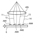
図8において、照明光源400(ファイバー等)から導光された光は、照明リレー光学系401、401'を通過する。照明系リレー光学系401、401'によって、ファイバー端面が後述する回転開口絞り415上に結像するように構成されている。尚、ここで、ファイバー端面、開口絞り415は後述する対物レンズの瞳位置PL(対物絞り)と共役な関係となっている。回転開口絞り415を通過した特定の光は、更に照明光学系402を通過した後、偏光ビームスプリッタ403に導かれる。偏光ビームスプリッタ403によって反射された紙面垂直なS偏光光は、リレーレンズ404、λ/4板409を通過した後、円偏光に変換され、対物レンズ405を通ってウエハ6上に形成されたアライメントマークAMをケーラー照明する。
【0034】
アライメントマークAMから発生した反射光、回折光、散乱光は、再度対物レンズ405、λ/4板409、リレーレンズ404を戻り、今度は紙面平行なP偏光に変換され、偏光ビームスプリッタ403を通過し、結像光学系410によって、アライメントマークAMの像を光電変換素子411(例えばCCDカメラ)上に形成する。光電変換されたアライメントマーク像の位置に基づいて、ウエハ6の位置を検出する。
【0035】
この時、ウエハ6上のアライメントマークAMを精度良く検出する為には、アライメントマークAMの像が鮮明に検出されなければならない。つまり、OA検出系4のピントがアライメントマークAMに合っていなければならない。
【0036】
その為に、一般的には不図示のAF検出系が構成されており、その検出結果に基づいて、アライメントマークをOA検出系のベストフォーカス面に駆動して、アライメントマークの検出を行っている。
【0037】
更に、ここで回転開口絞り415の役割について詳細に説明する。図8の回転開口絞り415の板材には特定の光が通過する空間的な絞りが複数構成されている。この回転開口絞り415は、回転駆動系420に構成されており、制御系421の指令に基づき、回転することで光路上に様々な絞り形状(415-a〜f)を交換、挿入することができる。尚、本図においては、白抜き部分が光を透過する領域で、斜線領域が遮光領域である。回転開口絞り415は、機械的な板材で構成しても良いし、ガラスにクロムのパターンが構成されている形状等でも良い。更に各絞り(415-a〜f)の大きさは、上記対物絞りPLの位置に換算した場合、対物絞りPLの大きさよりも等しいか又は小さいものである。また、各絞り(415-a〜f)に対するファイバー端面の大きさの関係は、ファイバー端面を回転開口絞り415上に換算した時にファイバー端面の方が大きくなる様に構成されている。
【0038】
また、これら開口絞り415は、その形状を異ならせるだけではなく、例えば、同じ形状でも一方には拡散板の様な光強度の面内分布を均一化する部材を構成しても良い。
【0039】
以上の様な構成で、回転開口絞り415の各絞り(415-a〜f)を選択することができ、OA検出系にとっての所謂照明σ或いは変形照明を可変にすることができる。照明σを変更する効果については別途以下に説明する。
【0040】
尚、絞り415-aは、対物絞りの大きさと同じ大きさに相当し、σ1と呼び、415-bは対物絞りPLよりも小さく(中σと呼ぶ)、415-cは更に小さい(小σと呼ぶ)。また、415-dは4重極照明、415-eはリング照明1、415-fはリング照明2として構成している。尚、実際のσ(絞り形状)は上記の構成に限定されておらず、OA検出系にとって最適な様々な形態を採っている。
【0041】
上記構成では、照明光源400(ファイバー)には、波長選択できる機構は記載されていないが、不図示の波長切替えフィルタを構成することで、OA検出系にとっての波長を選択することができる。
【0042】
波長及び照明σを可変にする効果を図2、図3を用いて更に説明する。
【0043】
図2(a)と図3(a)は共に、異なるアライメントマークを上から観察した模式図であり、計測方向は紙面横方向である。図2(b)と図3(b)はそれらアライメントマークの断面構造を示しており、積層しているプロセスは同じものと考える。また、斜線部はアライメント波長に対して、透明な層であると仮定している。図2(c)-(f)と図3(c)-(f)は、照明σ及び使用波長を変更した場合に得られるアライメントマーク検出信号を夫々示している。以下、照明σ、波長選択の組み合わせを「照明モード」と呼ぶ。
【0044】
図2(c)と図3(c)は、ある第1の中心波長を持つσ1で観察したときのアライメント検出信号、図2(d)と図3(d)は同じ波長でσを小σで観察したときのアライメント検出信号である。図2と図3の(e)、(f)は、σ1で波長を第2、3の中心波長を持つ場合のアライメント信号を示している。以上の様に、照明モードを変更することで、同じマークに対しても検出信号波形を可変にすることができる。更に、同じ照明モードでもマーク形状が変わることで、やはり得られるアライメント信号波形が変化する。
【0045】
尚、OA検出系は、図8に示す構成に限定されず、例えば、照明系の導光位置が異なる或いは、結像光学系410、光電変換素子411が複数構成されるといった検出系に対しても本発明を適用可能である。
【0046】
また、本例では、投影光学系とは別構成になっているOA検出系についてのみ説明したが、これに限定されるものではなく、投影光学系を介してウエハ上を観察するTTL―AA方式でも同様な構成は可能で、本発明を適用可能である。
【0047】
従来、アライメント検出系の性能を評価する方法として、ウエハステージ上のアライメントマークAM(ウエハ上に構成も可)をアライメント検出系で連続計測し、その計測再現性を用いて評価していた。或いは、実プロセスウエハの複数種のアライメントマークを選定する際には、同様にウエハステージ上のアライメントマークAMをアライメント検出系に対する再現性として評価し、その情報に基づいて選定していた。
【0048】
しかし、ウエハステージ上に構成されたアライメントマークAMの計測再現性では、ステージ位置の安定性が影響してしまい、アライメント検出系或いはアライメント信号としての評価にならない可能性がある。その理由として、通常ウエハステージは静止した状態の安定性は、実露光性能に対して余り重要な要素ではない。つまり、実露光時は、チップを次々に露光する(ステージを駆動する)状態で干渉計等が安定していれば良いからである。従って、ある意味では通常必要とされる使い方ではない状況で、アライメントマークAMの計測再現性の評価を行っていることになる。
【0049】
そこでアライメントマークの計測再現性の評価もマーク間隔の再現性として評価することで、純粋なアライメント検出系としての性能評価を行うことが可能となる。
【0050】
マーク間隔は、アライメントマーク自身の伸縮が無い限り、安定した状態にあって、常に一定の間隔である。たとえ伸縮があったとしても、熱的変形の為、複数回計測という短時間の計測の中で変動するものではない。また、マーク間隔も数μm〜数十μm程度である為、熱的伸縮では間隔変動は無視できる程度である。
【0051】
従って、マーク間隔の再現性を調べることで、ウエハステージの安定性に影響されず、正確にアライメント検出系の性能評価が可能となる。更には、複数種のアライメントマークに対し、マーク間隔の再現性として比較することで優れているアライメントマークを選定することが可能となる。
【0052】
更に別な観点として、図8に示されるようなアライメント検出系により、ウエハ6上のアライメントマークAMを光電変換した電気信号として検出する。図1にはウエハ6上に構成されたアライメントマークAMの模式図を示す。図1(a)は、アライメントマークAMをウエハ上方から見た状態を示し、図1(b)には、その光電変換された検出信号を示している。尚、本発明では、アライメントマークは2本以上の複数で構成されていれば、同様な効果が得られるが、本実施形態では、4本のアライメントマークを使用している。アライメントマークの計測方向は、各マーク(M1〜M4)の長手方向と垂直方向である。
【0053】
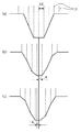
こうしたアライメントマークを計測方向に駆動しながら、計測していくと所謂デジタル誤差が発生する。このデジタル誤差を持っていると計測値が、非線形に変動してしまい、アライメント検出誤差となってしまう。その現象を図5と図6を参照して説明する。
【0054】
図5(a)は、1本のマークを計測方向に駆動した時の計測結果を模式的に表したものであり、検出系にデジタル誤差が発生しているとマークの位置に応じて、計測値が周期的に変化してしまう。図5(a)の横軸はアライメント検出系に対するマーク位置(例えば、ウエハステージの干渉計の読み値)であり、縦軸はアライメント検出系から得られるそのマークの計測値である。理想的には、直線的に変化するのが望ましい。図中のRDは計測値の生データを示しており、この生データ(周期的変化)に対して、直線近似したものがLDである。このLDに基づいて、直線成分からの残差をΔLとして示しているのが、図5(b)である。このようにマーク位置に対して計測誤差ΔLが発生してしまう場合、アライメント検出系に対して、どこにアライメントマークが存在するかによって計測値の誤差が変動してしまう。これでは、高精度なアライメント検出ができなくなる。
【0055】
ここで、もう少しデジタル誤差の発生メカニズムについて、図6を用いて説明する。
【0056】
図6は、図1に示すアライメントマーク1本に着目した検出信号波形を示している。また、図中の点線Dは、検出系のサンプリングポイントを示しており、CCDカメラの様な検出系の場合、画素サイズに相当し、レーザービームスキャンの様に時間的に信号をサンプリング検出する場合、そのサンプリング時間に相当する。尚、ここではCCDカメラの画素サイズとして説明する。CCDカメラで取り込まれたアライメント画像は、サンプリング間隔(画素サイズ)ΔDの間隔で、波形表示、検出される。図6(a)は、CCDカメラのある位置に対して、アライメントマークAMの位置が一致した状態で、図6(b)及び(c)は、CCDカメラ位置から1/4画素分ずれた位置にアライメントマークがある時のアライメントマークの検出信号波形を示している。尚、本例においては、アライメントマーク位置を変えずに、画素の位置を変更した場合として示している。従って、計測される位置(例えば、波形の重心位置)は、変化しないのが理想である。
【0057】
ところが、図6(b)と(c)では、1/4画素のずれる方向が(a)を境に反転しており、その為、アライメントマークの位置は変化していないにも関わらず、計測値は、ずれた方向に誤差Δ分だけ発生してしまう。つまり1画素内でアライメントマーク位置が変化すると、周期的に計測値がずれてしまうため、こうしたデジタル誤差を正しく評価する必要がある。従来こうしたデジタル誤差を計測する為に、ウエハステージ8上に構成されたアライメントマークをステージの干渉計を横軸に縦軸を計測値から算出していた。とことが、実際の干渉計では、空気の揺らぎ等があり、干渉計自体の安定性も含まれてしまっていた。
【0058】
そこで、本発明では、複数列のアライメントマークを使用して、その間隔に着目して、これらデジタル誤差を評価する。本実施形態の場合、図1のように、4本マークを使用して、それらの間隔SP1、SP2、SP3、SP4を用いて評価する。アライメント検出系に対するマーク位置に関して、デジタル誤差のある場合について、これらマーク計測値の変動(図7)とマーク間隔の変動(図9)の様子を模式的に示す。図7では、各マークの計測値がそれぞれ独立に変動していることが判る。実際のアライメントマークとアライメント検出系を考えた場合、アライメントマークの形状誤差や、アライメント検出系の倍率誤差等によって、CCDカメラの画素にかかる入り方が各マークで異なっている。従って、デジタル誤差の発生する位相は、この様に異なったものとなっている。通常、画素分解能は、0.1μm程度以下であり、それに対して、マークの間隔の絶対値も同程度の誤差を持っていると考えられる。或いは、アライメント検出系として、画素分解能とアライメントマークの間隔が同期しない様に設計値を制御している。そうすることで、デジタル誤差が、ランダムに発生し、できるだけトータル(4本マーク計測値の平均値)の計測値には、影響しない様に工夫する。但し、現実の検出系に対しては、検出系の製造誤差等がある為、これらの評価が必要となる。
【0059】
図9には、これら4本マークのそれぞれが比較的独立したデジタル誤差を持っている場合のマーク間隔変動を示している。この様に、マーク間隔(SP1〜SP4)も周期的に変化してしまう。
【0060】
この計測結果には、マーク間隔と言う不変の基準を用いている為、ステージの干渉計の誤差が載っておらず、従って、正確なデジタル誤差の測定が可能となる。
【0061】
以上の様に、これらステージを駆動した時のマーク間隔の変動量やマーク位置を固定した時のマーク間隔再現性を見ることで、アライメント検出系として或いはアライメント信号の純粋な精度評価を行うことが可能となる。
[第2実施形態]
次に、複数列のアライメントマークのマーク間隔の計測結果を用いて、実プロセスウエハのアライメントマーク或いは、照明モードの最適化について、図10、図11を用いて説明する。
【0062】
図10は、あるアライメントマークのマーク間隔の計測再現性(例えば、3σやレンジ)と、コントラスト(例えば、信号強度のMin/Max比)の関係を示している。このグラフからコントラストが高ければ、高いほどマーク間隔の計測再現性が向上する。つまり、複数列(4本)のマークの中心位置の計測再現性も向上することを意味している。このようになる1つの理由としては、光電変換素子からの光電変換信号の中に、電気処理系のノイズ成分が混入しており、コントラストの高い程、S/N比が改善されることが考えられる。従って、できるだけコントラストの高い照明モード或いは、アライメントマークを選択することで、計測再現性の向上が見込まれる。
【0063】
一方、図11は、コントラストとデジタル誤差との関係を示したグラフを表している。デジタル誤差の場合、1画素内で急峻に信号が変化(コントラストが高い)していると、画素と画素の境界領域で信号が飛ぶ為、コントラストが極端に高くなるとデジタル誤差も劣化してくることを示している。
【0064】
つまり、マークの計測再現性とデジタル誤差はコントラストに対して、測定精度が相反する方向に作用する。
【0065】
従って、上記マーク位置の計測再現性(マーク間隔再現性)とデジタル誤差の発生量の両方を考慮しながら、最適アライメントマーク或いは照明モードの選択が必要となる。
【0066】
尚、以上のようなマーク間隔の再現性やデジタル誤差といった性能は、CCDカメラの様なアライメントマークAMを像として検出する物に限定されないことは、上述したとおりである。
【0067】
例えば、アライメントアークAMに対して、スリット形状の照射ビームをスキャンし、回折、散乱した光によってマーク位置を検出するレーザービームスキャンタイプのアライメント検出系への適用も可能である。上記で示したCCDカメラの画素サイズは、レーザービームスキャンの場合、サンプリング時間に相当し、マーク間隔はあるマークを検出した時間と別なマークを検出した時間として、評価することで本発明の同様な効果を得られることは、明白であろう。
【0068】
更に、上記実施形態では、ウエハ上のアライメントマークAMを検出するアライメント検出系について言及してきたが、これに限定されるものでもない。例えば、レチクルの位置合わせを行うアライメント検出系(図3中11相当)への適用や、レチクル2、投影光学系3を通してレチクル上マークとウエハ上マークを同時に見る所謂TTR−AA(Through the Reticle)タイプのアライメント検出系(不図示)への本発明の適用は可能であることは明白である。
【0069】
次に、実プロセスウエハのアライメントマークの最適化と最適照明モードの選択方法について、図12、図13を用いて説明する。
【0070】
図12において、ウエハ処理が開始されると、ウエハのラフアライメント(メカプリアライメント)が行われる(ステップS12)。このラフアライメントは、その後のファインアライメント(所謂、グローバルアライメント)が行える精度で実行される。ファインアライメントでは、ウエハのショットレイアウトをアライメント検出系及びウエハステージの干渉計にて計測し、ショット(チップ)の配列情報が算出される(ステップS13)。
【0071】
その後、予め設定された特定ショットの第1のアライメントマーク(j=1)をアライメント検出位置に駆動する(ステップS14)。尚、この際、既に求められているショット配列情報に基づいて駆動される。
【0072】
一方、アライメント検出系は、ある第1の照明モード(i=1;照明σや使用波長)の設定を行う(ステップS15)。尚、何種類の照明モード、何種類のアライメントマークを使用するかは、ユーザーが予め設定できるようになっている。その設定の中で、第1番目のアライメントマークを第1の照明モードで計測するようになっている。
【0073】
第1のアライメントマークを第1の照明モードで観察している状態で、次にウエハのZ方向の計測(フォーカス計測)を行い、アライメント検出系にとって、BestFocus位置を算出した後、その位置に、ウエハを駆動する(ステップS16)。このオートフォーカスは、アライメントマークの検出波形のコントラストが最大になる位置や信号波形の微分値に着目して計測される。以上までで、第1アライメントマークを第1の照明モードでコントラストの高い状態で計測可能となる。
【0074】
次に、第1のアライメントマーク像から光電変換した検出信号を複数回取り込み、その各回の検出信号よりマーク間隔を算出し、それら計測値から再現性ΔSPij(i=1,j=1)及び、マーク間隔の絶対値SPijk(i=1,j=1,k=1)を算出する(ステップS17)。マーク間隔再現性の評価は、統計的な3σでも良いし、Rangeを使ってもよい。また、マーク間隔の絶対値SPijkは、複数回取り込んだ計測値の平均値とする。尚、計測回数については、予めユーザーが設定できるようになっても良いし、装置特定の回数としても良い。
【0075】
次に、ステージ微少駆動した後、上記ステップS17と同様にマーク間隔の絶対値SPijk(i=1,j=1,k=2)を算出する(ステップS18)。
【0076】
この際、計測再現性は算出しても、しなくても良く、算出しない場合、ステップS17で算出したマーク間隔再現性を第1アライメントマーク、第1照明モードの再現性とする。もし、再現性を再度算出する場合、計測再現性の平均値を第1アライメントマーク、第1照明モードの再現性として使用できる。即ち、
ΔSPij=ΣΔSPijk/k(max);k(max)は、Stage駆動回数
となる。
【0077】
ここで、ステージの微少駆動及びマーク間隔変動の算出部分(S17〜S19まで)について、図13を用いて、詳細に説明する。
【0078】
図13において、ステップS17の計測開始後、光電変換素子により、信号の取り込みを行い4本マークの各マーク位置を算出する。その時、複数回取り込むことは上述したとおりである(ステップS102)。その後、各マーク位置からマーク間隔(SPijk;i=1,j=1,k=1)を算出した後(ステップS103)、ウエハステージを微少駆動する(ステップS104)。駆動量は、予め設計値的に決めたものでも良く、或いはユーザーが設定できるものでも良い。何れの場合も、画素分解能よりも小さな量で駆動するのが望ましい。次に、駆動計測回数が所定の数だけ終わったかどうかの判断を行い、未達成の場合、ステップS102に戻り再度マーク間隔(SPijk;i=1,j=1,k=2〜)の算出を行う(ステップS105)。
【0079】
以上の様に、特定のStage駆動範囲で、Stageを微少駆動しながらマーク間隔の変動量ΔSPmaxijを算出する。尚、Stage駆動範囲についても、ユーザー設定、設計値設定が可能である。Stage駆動しながら、得られたマーク間隔の変動量ΔSPmaxijを第1アライメントマーク、第1照明モードの数字とする(ステップS106&S19)。図12に戻って、ここまでで、第1のアライメントマーク、第1の照明モードで、マーク間隔再現性ΔSPij(i=1,j=1)とマーク間隔変動量ΔSPmaxij(i=1,j=1)の2つの数字が得られた。
【0080】
その後、指定照明モードでの計測が完了したかの判断を行い(ステップS20)、未達成の場合、ステップS15に戻って別の照明モードへ切替えて、同様にΔSP2j、ΔSPM2jを算出する。
【0081】
指定照明モードでの評価が完了すると、次に複数種あるアライメントマークの評価が完了したかの判断を行う(ステップS21)。未完であれば、Stageを次のアライメントマーク位置に駆動して、同様に、ΔSPij、ΔSPmaxijを算出する。
【0082】
以上の様なシーケンスにより、複数のアライメントマークと複数の照明モードに対するΔSPijとΔSPmaxijを得ることができる。これら、ΔSPij、ΔSPmaxijに基づいて、最適アライメントマーク及び照明モード(最適条件)の算出を行うことが可能となる。
【0083】
尚、最適条件を算出する際、ΔSPijとΔSPmaxijのバランスについては、予め設定することができ、例えば、ΔSPij=ΔSPmaxijになる条件等で、その他その比率を変えても構わない。要するに、マーク間隔の再現性やマーク間隔変動に基づいて、最適条件を算出することに本発明の特徴がある。また、本例ではマーク間隔の変動量ΔSPmaxijは、変動量のレンジから算出しているが、これに限定されるものではなく、3σ等を用いても評価しても良い。
【0084】
上述の様にして、求められた最適アライメントマーク、最適照明モードを使用して、以下通常のアライメント動作及び露光が開始される。
【0085】
尚、本例では、1枚のウエハ、特定ショットを使った評価を行っているが、複数枚のウエハや、複数ショットで同様に評価して、その結果に基づいて最適条件を選定することも可能である。こうした測定を行う背景としては、ウエハ間でのプロセスばらつきが大きい場合やショット間でのばらつきが大きい場合に効果がある。特定ウエハや特定ショットでは最高値が得られるが、ばらつきが大きい場合、全てのウエハに対して最適とは限らない。従って、複数の情報を用いることで平均的に安定している最適条件を算出することが可能となる。
[第3実施形態]
次に、マーク間隔を使った別の実施形態について説明する。図14、15は、図8に示したアライメント検出系の対物レンズ405と対物絞りPL(物体面のフーリエ変換面;瞳)を夫々抜き出している。更に、ウエハ6上に構成されているアライメントマーク(AM1〜AM4)とそれらアライメントマークからの主光線(I1〜I4)を模式的に表現している。図14はそれぞれのアライメントマークから出た主光線(I1〜I4)が全て平行に且つウエハ面に対して垂直になるよう検出される様子を示している(所謂、軸外テレセンシティが良い状態にある)。
【0086】
一方、図15では対物レンズ405の製造誤差や不図示の照明系の入射光軸傾きや開口絞り415のFocus方向Zの位置ずれ等よって、軸外テレセンシティが悪い状態にあることを示している。この場合、各アライメントマークからの主光線(I1〜I4)が平行ではなく、且つウエハに対して垂直になっていない。
【0087】
こうした場合、ウエハのFocus方向Zの位置に対して、マーク間隔が変動してしまう。図14の場合、ウエハがデフォーカスした状態でも、マーク間隔の変化は発生せず、仮にデフォーカスした状態で、計測方向にマークがずれた場合でも、マーク間隔の変動は発生しない(リニアリティ残差が発生しない)。
【0088】
一方、図15に示す状態になっていると、デフォーカスするとマーク間隔が変化してしまい、更に軸外(像高別)でその主光線の傾きが異なる為、計測方向にマークを駆動した場合、マーク間隔の変動を発生してしまう(リニアリティ残差が発生してしまう)。
【0089】
ここで、軸外テレセンシティが悪く且つデフォーカスした状態で、マークを計測方向に駆動した場合の計測誤差(リニアリティ)について、図16を用いて説明する。軸外テレセンシティが悪く、デフォーカスした状態とは、あたかも検出範囲内でディストーション(歪曲収差)が発生しているのに相当する。つまり、検出範囲内で、画角に依存して、倍率が変化していることに相当する。そうした場合、マーク間隔の変動は、図16に示した様に、横軸をマーク計測方向に駆動した位置、縦軸にマーク間隔の変動を取ると、マーク間隔が狭まったり、広がったりした挙動を示す。こうした変化を持つ検出系において、4本マークの中心位置もマークが検出系のどこにあるかで計測値がずれてしまい、結果線形的な位置計測が出来なくなる(リニアリティ残差が発生する)。
【0090】
これでは、検出系に対するマークの送り込みを正確に行わなければ、その残差分だけ計測値のずれが発生し、結果アライメント精度を低下させてしまう。
【0091】
それを回避する方法としては、マークを常に所定の軸外に送り込んで計測する方法(クローズ追込み計測)も考えられるが、これではスループットの低下を招いてしまい、装置としてデメリットを持ってしまう。従って、検出範囲内でできるだけリニアリティ残差の少ない計測が重要となる。
【0092】
この図15の様に、軸外テレセンシティが悪くなってしまう理由としては、図17に示すように、対物レンズの瞳の結像トレースをした時の瞳面上での球面収差が発生している場合等がある(瞳の球面収差が悪い)。各像高から出てきた平行な主光線が、瞳面上で集光せずに、球面収差を持ってしまっている。その他、照明系としての瞳の球面収差がある場合や、瞳の位置がFocus方向にずれている場合(開口絞り415位置がずれている場合)等がある。
【0093】
以上の様に軸外テレセンシティが悪く、アライメントマークが検出系に対して、デフォーカスして計測するとリニアリティの残差が発生してしまい、アライメント精度の劣化を発生してしまう。そこで、この軸外テレセンシティを測定し、調整する必要がある。
【0094】
複数列で構成されているアライメントマーク(本実施形態では、4本)を使って、ウエハをFocus方向Zに駆動し、各Z位置に対してマーク間隔を計測すればよい。その一例を図18に示す。図18では、4本の主光線(I1〜I4)の全てが傾きを持っており、どれも平行でない場合を想定している。更に、I2とI3の傾き量の絶対値が異なっている場合を想定している。横軸には、ウエハのZ位置を示し、縦軸には、BestFocus位置のマーク間隔を基準とした時のマーク間隔変化の様子を表している。この様に、軸外テレセンシティが悪い場合、マーク間隔がZに対して、変化してしまう。こうした検出系の調整状態で、デフォーカスした位置でリニアリティを測定すると、検出系に対するマーク位置に対して、計測リニアリティの残差成分が発生してしまう。
【0095】
現実的な露光装置においてのアライメント検出系を考えた場合、実プロセスウエハのレジスト膜厚ばらつき等で、BestFocus位置がウエハやチップに依って、多少変化する可能性がある。そうした場合、結果としてデフォーカスした状態で計測される為、上記の様な誤差成分は極力小さくしなくてはならない。
【0096】
図18に示すように、ウエハをFocus方向Z振りながら、マーク間隔を計測することで、発生している軸外テレセンシティを観察でき、マーク間隔の変動が発生しないように、アライメント検出系を調整する。
【0097】
調整方法としては、対物絞りPLの位置をFocus方向Zに調整するとか、光軸と直交する方向に調整するなどが考えられる。更には、照明系の中に構成されている開口絞り(図8中415)のFocus調整によっても同様な効果が得られる。或いは、対物レンズ自体に調整機構を設け瞳の球面収差を調整したりすることでも可能で、何れの方法でも良く、本発明の特徴はウエハをFocus方向Zに振りながら、マーク間隔を計測することにある。
【0098】
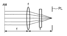
ここで、対物絞りPLの位置調整により、軸外テレセンシティを調整する方法を図19に基づいて説明する。尚、本例では、先の瞳の球面収差は存在せず、薄肉系の光学系として説明する。図19(a)は、理想的なアライメントマーク位置と対物レンズ405と対物絞りPLの位置関係を示している。対物レンズ405の焦点距離をfとした場合、対物絞りPLの位置を対物レンズからfの位置に配置することで、全ての画角の主光線I1〜I4が平行になる。つまり軸外テレセンシティが良好な状態になる。ところが、対物絞りPLがfの位置からずれてしまっている場合(図19(b),(c))、主光線I1'〜I4'はもはや平行にはならなくなる。つまり軸外テレセンシティが崩れた(悪く)状態になる。これでは、アライメントマークAMがデフォーカスしてしまうとマーク間隔が変動してしまい、更にデフォーカスしたままリニアリティを計測するとリニアリティ残差を発生してしまう。
【0099】
対物絞りPLの位置調整は、この対物絞りPLの位置を理想的なfの位置になるようにする。その際、デフォーカスしながらマーク間隔の変動(図18)を見ることで、軸外テレセンシティが観察可能となる。この図18に示すグラフにおいて、全てのマーク間隔変動の傾きが無くなるように調整すればよい。
【0100】
以上では、対物絞りPLをFocus方向Zに調整した例を示したがこれに、限定されるものではなく、
対物絞りPLと共役位置に配置した別の絞りをFocus方向に調整しても同じ効果が得られる。具体的には、図3に示す回転開口絞り415をFocus方向に調整しても同様な効果が得られる。
【0101】
又、瞳の球面収差を取る形態として、図20に一例を示す。
【0102】
本例では、対物レンズ405と対物絞りPLの間にガラスを構成した例を示している。対物レンズ405の設計値(瞳の球面収差の出方等)によってこのガラス部材は様々な形態を取る。単純なガラス板で構成することが可能な場合もあるし、曲率を持たせた(所謂レンズ)を挿入することでも補正は可能である。何れにしても、こうした光学部材を対物絞り近傍に配置することで、瞳の球面収差を補正することが出来、結果軸外テレセンシティの補正、調整が可能となる。実際の調整では、マーク間隔変動量を見ながら、ガラスの板厚を変更したり、曲率を変更することで、製造上で発生する瞳の球面収差も補正が可能である。
【0103】
以上の様に、アライメントマークをFocus方向Zに駆動し、各Z位置でのマーク間隔をプロットしていくことで、所謂軸外テレセンシティが観察でき、この軸外テレセンシティを良くする(全ての画角の主光線について、マークに垂直に入射している)ことで、マークデフォーカス時の計測においても、リニアリティ残差が発生しなく、高精度ない位置検出が可能となる。
【0104】
以上の各実施形態は、OA検出系に限定されないことは明白であろう。つまり、投影光学系を介して、ウエハ上のアライメントマークAMを観察するアライメント検出系やレチクル位置を検出するアライメント検出系、レチクルとウエハとを投影光学系を介して検出するTTR−AA系にも適用可能である。
【0105】
また、上記アライメント検出系を半導体露光装置や液晶露光装置に適用することで高精度な位置検出が可能な装置を提供できる。
[半導体生産システムの実施形態]
次に、本発明に係わる露光装置を用いた半導体デバイス(ICやLSI等の半導体チップ、液晶パネル、CCD、薄膜磁気ヘッド、マイクロマシン等)の生産システムの例を説明する。これは半導体製造工場に設置された製造装置のトラブル対応や定期メンテナンス、あるいはソフトウェア提供などの保守サービスを、製造工場外のコンピュータネットワークを利用して行うものである。
【0106】
図21は全体システムをある角度から切り出して表現したものである。図中、101は半導体デバイスの製造装置を提供するベンダ(装置供給メーカ)の事業所である。製造装置の実例としては、半導体製造工場で使用する各種プロセス用の半導体製造装置、例えば、前工程用機器(露光装置、レジスト処理装置、エッチング装置等のリソグラフィ装置、熱処理装置、成膜装置、平坦化装置等)や後工程用機器(組立て装置、検査装置等)を想定している。事業所101内には、製造装置の保守データベースを提供するホスト管理システム108、複数の操作端末コンピュータ110、これらを結んでイントラネット等を構築するローカルエリアネットワーク(LAN)109を備える。ホスト管理システム108は、LAN109を事業所の外部ネットワークであるインターネット105に接続するためのゲートウェイと、外部からのアクセスを制限するセキュリティ機能を備える。
【0107】
一方、102〜104は、製造装置のユーザとしての半導体製造メーカの製造工場である。製造工場102〜104は、互いに異なるメーカに属する工場であっても良いし、同一のメーカに属する工場(例えば、前工程用の工場、後工程用の工場等)であっても良い。各工場102〜104内には、夫々、複数の製造装置106と、それらを結んでイントラネット等を構築するローカルエリアネットワーク(LAN)111と、各製造装置106の稼動状況を監視する監視装置としてホスト管理システム107とが設けられている。各工場102〜104に設けられたホスト管理システム107は、各工場内のLAN111を工場の外部ネットワークであるインターネット105に接続するためのゲートウェイを備える。これにより各工場のLAN111からインターネット105を介してベンダ101側のホスト管理システム108にアクセスが可能となり、ホスト管理システム108のセキュリティ機能によって限られたユーザだけにアクセスが許可となっている。具体的には、インターネット105を介して、各製造装置106の稼動状況を示すステータス情報(例えば、トラブルが発生した製造装置の症状)を工場側からベンダ側に通知する他、その通知に対応する応答情報(例えば、トラブルに対する対処方法を指示する情報、対処用のソフトウェアやデータ)や、最新のソフトウェア、ヘルプ情報などの保守情報をベンダ側から受け取ることができる。各工場102〜104とベンダ101との間のデータ通信および各工場内のLAN111でのデータ通信には、インターネットで一般的に使用されている通信プロトコル(TCP/IP)が使用される。なお、工場外の外部ネットワークとしてインターネットを利用する代わりに、第三者からのアクセスができずにセキュリティの高い専用線ネットワーク(ISDNなど)を利用することもできる。また、ホスト管理システムはベンダが提供するものに限らずユーザがデータベースを構築して外部ネットワーク上に置き、ユーザの複数の工場から該データベースへのアクセスを許可するようにしてもよい。
【0108】
さて、図22は本実施形態の全体システムを図21とは別の角度から切り出して表現した概念図である。先の例ではそれぞれが製造装置を備えた複数のユーザ工場と、該製造装置のベンダの管理システムとを外部ネットワークで接続して、該外部ネットワークを介して各工場の生産管理や少なくとも1台の製造装置の情報をデータ通信するものであった。これに対し本例は、複数のベンダの製造装置を備えた工場と、該複数の製造装置のそれぞれのベンダの管理システムとを工場外の外部ネットワークで接続して、各製造装置の保守情報をデータ通信するものである。図中、201は製造装置ユーザ(半導体デバイス製造メーカ)の製造工場であり、工場の製造ラインには各種プロセスを行う製造装置、ここでは例として露光装置202、レジスト処理装置203、成膜処理装置204が導入されている。なお図22では製造工場201は1つだけ描いているが、実際は複数の工場が同様にネットワーク化されている。工場内の各装置はLAN206で接続されてイントラネットを構成し、ホスト管理システム205で製造ラインの稼動管理がされている。
【0109】
一方、露光装置メーカ210、レジスト処理装置メーカ220、成膜装置メーカ230などベンダ(装置供給メーカ)の各事業所には、それぞれ供給した機器の遠隔保守を行うためのホスト管理システム211,221,231を備え、これらは上述したように保守データベースと外部ネットワークのゲートウェイを備える。ユーザの製造工場内の各装置を管理するホスト管理システム205と、各装置のベンダの管理システム211,221,231とは、外部ネットワーク200であるインターネットもしくは専用線ネットワークによって接続されている。このシステムにおいて、製造ラインの一連の製造機器の中のどれかにトラブルが起きると、製造ラインの稼動が休止してしまうが、トラブルが起きた機器のベンダからインターネット200を介した遠隔保守を受けることで迅速な対応が可能で、製造ラインの休止を最小限に抑えることができる。
【0110】
半導体製造工場に設置された各製造装置はそれぞれ、ディスプレイと、ネットワークインタフェースと、記憶装置にストアされたネットワークアクセス用ソフトウェアならびに装置動作用のソフトウェアを実行するコンピュータを備える。記憶装置としては内蔵メモリやハードディスク、あるいはネットワークファイルサーバーなどである。上記ネットワークアクセス用ソフトウェアは、専用又は汎用のウェブブラウザを含み、例えば図23に一例を示す様な画面のユーザインタフェースをディスプレイ上に提供する。各工場で製造装置を管理するオペレータは、画面を参照しながら、製造装置の機種301、シリアルナンバー302、トラブルの件名303、発生日304、緊急度305、症状306、対処法307、経過308等の情報を画面上の入力項目に入力する。入力された情報はインターネットを介して保守データベースに送信され、その結果の適切な保守情報が保守データベースから返信されディスプレイ上に提示される。またウェブブラウザが提供するユーザインタフェースはさらに図示のごとくハイパーリンク機能310〜312を実現し、オペレータは各項目の更に詳細な情報にアクセスしたり、ベンダが提供するソフトウェアライブラリから製造装置に使用する最新バージョンのソフトウェアを引出したり、工場のオペレータの参考に供する操作ガイド(ヘルプ情報)を引出したりすることができる。ここで、保守データベースが提供する保守情報には、上記説明した本発明に関する情報も含まれ、また前記ソフトウェアライブラリは本発明を実現するための最新のソフトウェアも提供する。
【0111】
次に上記説明した生産システムを利用した半導体デバイスの製造プロセスを説明する。図24は半導体デバイスの全体的な製造プロセスのフローを示す。ステップS201(回路設計)では半導体デバイスの回路設計を行う。ステップS202(マスク製作)では設計した回路パターンを形成したマスクを製作する。一方、ステップS203(ウエハ製造)ではシリコン等の材料を用いてウエハを製造する。ステップS204(ウエハプロセス)は前工程と呼ばれ、上記用意したマスクとウエハを用いて、リソグラフィ技術によってウエハ上に実際の回路を形成する。次のステップS205(組み立て)は後工程と呼ばれ、ステップS204によって作製されたウエハを用いて半導体チップ化する工程であり、アッセンブリ工程(ダイシング、ボンディング)、パッケージング工程(チップ封入)等の組立て工程を含む。ステップS206(検査)ではステップS205で作製された半導体デバイスの動作確認テスト、耐久性テスト等の検査を行う。こうした工程を経て半導体デバイスが完成し、これを出荷(ステップS207)する。前工程と後工程はそれぞれ専用の別の工場で行い、これらの工場毎に上記説明した遠隔保守システムによって保守がなされる。また前工程工場と後工程工場との間でも、インターネットまたは専用線ネットワークを介して生産管理や装置保守のための情報がデータ通信される。
【0112】
図25は上記ウエハプロセスの詳細なフローを示す。ステップS211(酸化)ではウエハの表面を酸化させる。ステップS212(CVD)ではウエハ表面に絶縁膜を成膜する。ステップS213(電極形成)ではウエハ上に電極を蒸着によって形成する。ステップS214(イオン打込み)ではウエハにイオンを打ち込む。ステップS215(レジスト処理)ではウエハに感光剤を塗布する。ステップS216(露光)では上記説明した露光装置によってマスクの回路パターンをウエハに焼付露光する。ステップS217(現像)では露光したウエハを現像する。ステップS218(エッチング)では現像したレジスト像以外の部分を削り取る。ステップS219(レジスト剥離)ではエッチングが済んで不要となったレジストを取り除く。これらのステップを繰り返し行うことにより、ウエハ上に多重に回路パターンを形成する。各工程で使用する製造機器は上記説明した遠隔保守システムによって保守がなされているので、トラブルを未然に防ぐと共に、もしトラブルが発生しても迅速な復旧が可能で、従来に比べて半導体デバイスの生産性を向上させることができる。
【0113】
【発明の効果】
以上説明したように、本発明によれば、マーク間隔というウエハステージの安定性に左右されない計測値を用いることで、正確なマーク検出性能評価が可能となる。併せて、マーク間隔の再現性、マークを駆動した際のマーク間隔変動を計測すれば、最適なアライメントマーク、照明モードの選定が可能となる。更に、アライメントマークをデフォーカスしながらマーク間隔の変化を見れば、アライメント検出系の軸外テレセンシティを観察し、軸外テレセンシティが最良になるよう調整できる。また、そうすることで、アライメントマークをデフォーカスした状態で計測を行っても、計測方向のリニアリティが保証され高精度な位置検出が可能となる。
【図面の簡単な説明】
【図1】アライメントマークの間隔計測と検出信号波形について示す模式図である。
【図2】第1アライメントマークと照明モード変更による検出信号波形の模式図である。
【図3】第2アライメントマークと照明モード変更による検出信号波形の模式図である。
【図4】アライメント検出系を備えた投影露光装置の概略図である。
【図5】アライメントマーク位置に対するデジタル誤差を示す模式図である。
【図6】アライメントマーク検出信号波形とデジタル誤差の発生メカニズムを示す模式図である。
【図7】アライメントマーク位置に対するデジタル誤差を示す模式図である。
【図8】オフアクシスアライメント検出系を示す概略図である。
【図9】アライメントマーク位置に対するマーク間隔変動を示す概略図である。
【図10】計測再現性とコントラストを示す模式図である。
【図11】デジタル誤差とコントラストを示す模式図である。
【図12】最適アライメントマークと照明モードを選定する手順を示すフローチャートである。
【図13】最適アライメントマークと照明モードを選定する手順を示すフローチャートである。
【図14】軸外テレセンシティの良好な模式図である。
【図15】軸外テレセンシティの悪い場合の模式図である。
【図16】軸外テレセンシティが悪くデフォーカス計測時のアライメントマーク計測位置を示す模式図である。
【図17】瞳の球面収差を示す模式図である。
【図18】軸外テレセンシティが悪くデフォーカス計測時のマーク間隔変動を示す模式図である。
【図19】対物絞りPL位置と軸外テレセンシティの関係を示す模式図である。
【図20】瞳の球面収差を補正する一例を示す模式図である。
【図21】本発明に係わる露光装置を用いた半導体デバイスの生産システムをある角度から見た概念図である。
【図22】本発明に係わる露光装置を用いた半導体デバイスの生産システムを別の角度から見た概念図である。
【図23】ユーザインタフェースの具体例である。
【図24】デバイスの製造プロセスのフローを説明する図である。
【図25】ウエハプロセスを説明する図である。
【符号の説明】
1 投影露光照明系
2 レチクル
3 投影露光光学系
4 OA検出系
5 AF検出系
6 ウエハ
7 干渉計ミラー
8 ウエハステージ
9 干渉計
10 ステージ制御部
11 レチクルアライメント検出系
12,12' レチクルフォルダ
13 基準マーク
14 制御部
101 ベンダの事業所
102,103,104 製造工場
105 インターネット
106 製造装置、
107 工場のホスト管理システム
108 ベンダ側のホスト管理システム
109 ベンダ側のローカルエリアネットワーク(LAN)
110 操作端末コンピュータ
111 工場のローカルエリアネットワーク(LAN)
200 外部ネットワーク
201 製造装置ユーザの製造工場
202 露光装置
203 レジスト処理装置
204 成膜処理装置
205 工場のホスト管理システム
206 工場のローカルエリアネットワーク(LAN)
210 露光装置メーカ
211 露光装置メーカの事業所のホスト管理システム
220 レジスト処理装置メーカ
221 レジスト処理装置メーカの事業所のホスト管理システム
230 成膜装置メーカ
231 成膜装置メーカの事業所のホスト管理システム
301 製造装置の機種
302 シリアルナンバー
303 トラブルの件名
304 発生日
305 緊急度
306 症状
307 対処法
308 経過
310〜312 ハイパーリンク機能
401 アライメント光源
402 照明光学系
403 偏光ビームスプリッタ
404 リレーレンズ
405 対物レンズ
409 λ/4板
410 結像光学系
411 光電変換素子(検出面)[0001]
BACKGROUND OF THE INVENTION
The present invention provides position detection capable of detecting and aligning a wafer with high accuracy by observing a detection target image formed on a wafer or the like when manufacturing various devices such as semiconductor ICs, LSIs, CCDs, liquid crystal panels, and magnetic heads. The present invention relates to a method, a position detection apparatus, an exposure apparatus, and an exposure method.
[0002]
[Prior art]
Recently, the progress of semiconductor device manufacturing technology has been remarkable, and the progress of microfabrication technology has been remarkable. In particular, optical processing technology is mainly reduced projection exposure equipment with submicron resolution, commonly known as steppers. To further improve resolution, the numerical aperture (NA) of the optical system is increased and the exposure wavelength is shortened. It has been.
[0003]
As the exposure wavelength is shortened, the exposure light source is also changing from g-line and i-line high-pressure mercury lamps to KrF and ArF excimer lasers.
[0004]
On the other hand, with the improvement of the resolution of the projection pattern, higher accuracy is also required for the alignment for relative alignment of the wafer and the mask (reticle) in the projection exposure apparatus. A projection exposure apparatus is not only a high-resolution exposure apparatus but also a function as a highly accurate position detection apparatus.
[0005]
For this reason, the performance of a position detection device for detecting an alignment mark formed on a wafer or the like, that is, a so-called alignment scope itself is required to be highly accurate.
[0006]
Two types of alignment scopes have been proposed and used. One is a so-called off-axis alignment detection system (hereinafter referred to as “OA”) that is configured separately without using a projection exposure optical system and optically detects alignment marks.
[0007]
As an alignment method in a conventional i-line exposure apparatus, a method for detecting alignment marks on a wafer using an alignment wavelength of non-exposure light via a projection light optical system called TTL-AA (Through the Lens Auto Alignment) There is.
[0008]
Currently, in any detection system, a method of converting an image (image data) of an alignment mark to be observed into an electrical signal by a photoelectric conversion element and calculating a position based on the electrical signal is accurate or It is becoming mainstream due to its flexibility for various semiconductor processes.
[0009]
A projection exposure optical system equipped with a conventional OA detection system will be described with reference to a schematic diagram shown in FIG.
[0010]
Light IL emitted from an exposure illumination
[0011]
The image passing through the reticle pattern is transferred by the projection exposure optical system 3 to the
[0012]
On the other hand, the
[0013]
Here, an alignment method including an OA detection system will be described with reference to FIG.
[0014]
As shown in FIG. 4, the
[0015]
Next, based on the arrangement information of the chips (elements), the
[0016]
Here, in the exposure area of the normal projection exposure optical system 3, a
[0017]
The slit pattern projected on the
[0018]
In the projection exposure apparatus as described above, the alignment mark AM formed on the
[0019]
The explanation of the TTL-AA method is omitted here, but basically there are various points except that the OA detection system is configured to observe the wafer via the projection optical system. The alignment mark can be detected by changing illumination conditions.
[0020]
[Problems to be solved by the invention]
However, when the position on the wafer is detected by observing the mark using the alignment scope as described above, the alignment detection signal obtained varies depending on the structure (vertical structure, horizontal structure) and type of the alignment mark. In order to enable highly accurate detection, it is necessary to optimize the illumination mode. For this reason, the apparatus side is required to select an optimum alignment mark structure and illumination mode for various wafer processes and to recommend them to the user.
[0021]
Conventionally, when selecting the optimal illumination mode for these various processes, the selection is made only by the contrast of the obtained alignment detection signal waveform, and as a result, the consistency with the final alignment accuracy cannot be obtained. There is a case.
[0022]
Furthermore, when evaluating the performance of the alignment scope, the alignment marks (including the configuration on the wafer) formed on the wafer stage are continuously measured and judged from their reproducibility (eg, 3σ and range). It was. However, in this case, there is a problem that the performance of the alignment detection system originally desired could not be evaluated well due to the stability of the wafer stage itself (interferometer stability, etc.).
[0023]
Furthermore, linearity (linearity of the measured value when the alignment mark is driven in the measurement direction), which is one of the performances of the alignment detection system, is not possible, and deviation from the linearity (hereinafter referred to as “linearity residual”). Called). On the other hand, a method for identifying and adjusting the cause has not been established.
[0024]
If the measurement accuracy (linearity) of the alignment mark position with respect to such a measurement direction deteriorates, the alignment mark must be sent to a predetermined position with respect to the alignment detection system, resulting in a decrease in throughput.
[0025]
The present invention has been made in view of the above problems, and an object thereof is to provide a position detection method, a position detection apparatus, an exposure apparatus and an exposure method, and a device manufacturing method that enable accurate mark position detection performance evaluation. .
[0026]
[Means for Solving the Problems]
The present invention solves the problems of the alignment detection system as described above, by adjusting the mark interval of the alignment marks arranged on the observation object by the alignment detection system that detects the position of the observation object. More than once By measuring and evaluating the measurement reproducibility of the alignment detection system based on the mark interval information obtained as a result of this measurement, a pure alignment detection system that could not be evaluated accurately due to the influence of the stability of the wafer stage. It is possible to accurately evaluate the performance of the.
[0027]
Furthermore, the mark interval information means that the alignment mark is continuously measured at a stationary position, and the mark interval is reproducible (hereinafter referred to as “mark interval reproducibility”), or the alignment mark is driven at multiple positions while driving in the measurement direction. Then, the mark interval is measured, and the mark interval fluctuation amount obtained therefrom (hereinafter referred to as “mark interval stability”) is obtained.
[0028]
Further, by paying attention to the mark interval reproducibility and mark interval stability, it is possible to select an optimum alignment mark and an optimum illumination condition (illumination σ, NA, wavelength, etc.) for an actual process wafer. As a result, it is possible to improve the alignment accuracy on the actual process wafer.
[0029]
Furthermore, a plurality of alignment marks arranged on the observation object are moved relative to the alignment detection system in the focus direction by an alignment detection system for detecting the position of the observation object, and marks at a plurality of relative positions are used. The distance is calculated, the amount of fluctuation is calculated from the mark interval information at the plurality of relative positions, and the defocus magnification and Dist change (hereinafter referred to as “off-axis telecentricity”) of the alignment detection system are calculated from the amount of fluctuation. By adjusting, it is possible to improve the linearity accuracy at the time of alignment mark defocus measurement.
[0030]
As described above, since the evaluation is performed based on the invariable standard of the mark interval, it is possible to provide an alignment detection system with higher accuracy than in the past.
[0031]
Further, by applying the alignment detection system to a semiconductor exposure apparatus or a liquid crystal exposure apparatus, a method for manufacturing a device such as a semiconductor capable of highly accurate position detection can be provided.
[0032]
DETAILED DESCRIPTION OF THE INVENTION
Embodiments according to the present invention will be described below in detail with reference to the accompanying drawings.
[First Embodiment]
The OA detection system (alignment detection system) 4 of the projection exposure apparatus shown in FIG. 4 will be described with reference to the detailed view of FIG.
[0033]
In FIG. 8, the light guided from the illumination light source 400 (fiber or the like) passes through the illumination relay
[0034]
Reflected light, diffracted light, and scattered light generated from the alignment mark AM return to the
[0035]
At this time, in order to accurately detect the alignment mark AM on the
[0036]
For this purpose, an AF detection system (not shown) is generally configured, and based on the detection result, the alignment mark is detected by driving the alignment mark to the best focus surface of the OA detection system. .
[0037]
Further, the role of the
[0038]
Further, these aperture stops 415 are not only different in shape, but may be configured to have a uniform in-plane distribution of light intensity, such as a diffuser plate, for example, even in the same shape.
[0039]
With the configuration as described above, each stop (415-a to f) of the
[0040]
The aperture 415-a corresponds to the same size as the objective aperture and is referred to as σ1, 415-b is smaller than the objective aperture PL (referred to as medium σ), and 415-c is smaller (small σ). Called). Further, 415-d is configured as quadrupole illumination, 415-e is configured as
[0041]
In the above configuration, the illumination light source 400 (fiber) does not describe a mechanism capable of selecting a wavelength. However, a wavelength switching filter (not shown) can be configured to select a wavelength for the OA detection system.
[0042]
The effect of making the wavelength and illumination σ variable will be further described with reference to FIGS.
[0043]
FIG. 2A and FIG. 3A are both schematic views of different alignment marks observed from above, and the measurement direction is the horizontal direction of the drawing. FIG. 2B and FIG. 3B show the cross-sectional structure of these alignment marks, and the process of laminating is considered to be the same. In addition, it is assumed that the hatched portion is a transparent layer with respect to the alignment wavelength. 2 (c)-(f) and FIG. 3 (c)-(f) show alignment mark detection signals obtained when the illumination σ and the used wavelength are changed. Hereinafter, the combination of illumination σ and wavelength selection is referred to as “illumination mode”.
[0044]
2 (c) and 3 (c) are alignment detection signals when observed at σ1 having a certain first central wavelength, and FIGS. 2 (d) and 3 (d) show a small σ at the same wavelength. This is an alignment detection signal when observed with. (E) and (f) of FIGS. 2 and 3 show alignment signals in the case where σ1 has a wavelength and second and third center wavelengths. As described above, the detection signal waveform can be made variable for the same mark by changing the illumination mode. Furthermore, the alignment signal waveform obtained also changes as the mark shape changes even in the same illumination mode.
[0045]
Note that the OA detection system is not limited to the configuration shown in FIG. 8. For example, the detection system in which the light guide position of the illumination system is different or the imaging
[0046]
In addition, in this example, only the OA detection system having a configuration different from that of the projection optical system has been described. However, the present invention is not limited to this, and the TTL-AA method for observing the wafer via the projection optical system. However, a similar configuration is possible and the present invention can be applied.
[0047]
Conventionally, as a method for evaluating the performance of the alignment detection system, the alignment mark AM (which can be configured on the wafer) on the wafer stage is continuously measured by the alignment detection system, and evaluation is performed using the measurement reproducibility. Alternatively, when selecting a plurality of types of alignment marks on an actual process wafer, the alignment marks AM on the wafer stage are similarly evaluated as reproducibility with respect to the alignment detection system and selected based on the information.
[0048]
However, the measurement reproducibility of the alignment mark AM configured on the wafer stage is affected by the stability of the stage position, and may not be evaluated as an alignment detection system or an alignment signal. For this reason, the stability of the stationary state of the normal wafer stage is not a very important factor for the actual exposure performance. That is, at the time of actual exposure, it is sufficient that the interferometer or the like is stable in a state where the chips are successively exposed (the stage is driven). Therefore, in a sense, the measurement reproducibility of the alignment mark AM is evaluated in a situation that is not normally required.
[0049]
Therefore, by evaluating the measurement reproducibility of the alignment mark as the reproducibility of the mark interval, it is possible to perform the performance evaluation as a pure alignment detection system.
[0050]
The mark interval is in a stable state as long as the alignment mark itself does not expand and contract, and is always a constant interval. Even if there is expansion and contraction, it does not fluctuate in a short measurement such as multiple measurements due to thermal deformation. In addition, since the mark interval is about several μm to several tens of μm, the interval variation is negligible in the thermal expansion and contraction.
[0051]
Therefore, by examining the reproducibility of the mark interval, the performance of the alignment detection system can be accurately evaluated without being affected by the stability of the wafer stage. Furthermore, it is possible to select an excellent alignment mark by comparing the reproducibility of the mark interval with respect to a plurality of types of alignment marks.
[0052]
As yet another viewpoint, the alignment mark AM on the
[0053]
If measurement is performed while driving these alignment marks in the measurement direction, a so-called digital error occurs. If this digital error is present, the measured value fluctuates nonlinearly, resulting in an alignment detection error. This phenomenon will be described with reference to FIGS.
[0054]
FIG. 5 (a) schematically shows the measurement result when one mark is driven in the measurement direction. If a digital error occurs in the detection system, the measurement is performed according to the mark position. The value changes periodically. The horizontal axis of FIG. 5A is the mark position (for example, the reading value of the interferometer of the wafer stage) with respect to the alignment detection system, and the vertical axis is the measurement value of the mark obtained from the alignment detection system. Ideally, it should change linearly. RD in the figure shows raw data of measured values, and LD is a linear approximation of this raw data (periodic change). FIG. 5B shows the residual from the linear component as ΔL based on the LD. Thus, when the measurement error ΔL occurs with respect to the mark position, the error of the measurement value varies depending on where the alignment mark is present in the alignment detection system. This makes it impossible to detect alignment with high accuracy.
[0055]
Here, the generation mechanism of the digital error is described with reference to FIG.
[0056]
FIG. 6 shows a detection signal waveform focusing on one alignment mark shown in FIG. The dotted line D in the figure indicates the sampling point of the detection system. In the case of a detection system such as a CCD camera, this corresponds to the pixel size, and when a signal is sampled and detected temporally as in a laser beam scan. , Corresponding to the sampling time. Here, the pixel size of the CCD camera will be described. The alignment image captured by the CCD camera is displayed and detected at a sampling interval (pixel size) ΔD. FIG. 6A shows a state in which the position of the alignment mark AM coincides with a certain position of the CCD camera, and FIGS. 6B and 6C show a position shifted by 1/4 pixel from the CCD camera position. The detection signal waveform of the alignment mark when there is an alignment mark is shown. In this example, the pixel position is changed without changing the alignment mark position. Therefore, it is ideal that the position to be measured (for example, the position of the center of gravity of the waveform) does not change.
[0057]
However, in FIGS. 6 (b) and 6 (c), the direction in which the 1/4 pixel shifts is reversed with respect to (a), and therefore the alignment mark position is not changed, but the measurement is performed. The value is generated by an error Δ in the shifted direction. In other words, if the alignment mark position changes within one pixel, the measured value is periodically shifted, so it is necessary to correctly evaluate such a digital error. Conventionally, in order to measure such a digital error, the alignment mark formed on the wafer stage 8 is calculated from the measured value on the horizontal axis of the interferometer of the stage and the vertical axis. However, the actual interferometer has air fluctuations and the stability of the interferometer itself has been included.
[0058]
Therefore, in the present invention, these digital errors are evaluated by using a plurality of alignment marks and paying attention to the interval. In the case of the present embodiment, as shown in FIG. 1, evaluation is performed using four marks and using their intervals SP1, SP2, SP3, and SP4. With respect to the mark position with respect to the alignment detection system, in the case where there is a digital error, the state of these mark measurement value fluctuations (FIG. 7) and mark interval fluctuations (FIG. 9) is schematically shown. In FIG. 7, it can be seen that the measured values of the respective marks are varied independently. When an actual alignment mark and an alignment detection system are considered, how to enter the pixels of the CCD camera differs depending on the shape of the alignment mark, magnification error of the alignment detection system, and the like. Accordingly, the phase in which the digital error occurs is thus different. Usually, the pixel resolution is about 0.1 μm or less, and the absolute value of the mark interval is considered to have the same error. Alternatively, as an alignment detection system, the design value is controlled so that the pixel resolution and the alignment mark interval are not synchronized. By doing so, a digital error is generated at random, and it is devised so as not to affect the total (average value of four mark measurement values) as much as possible. However, since there are manufacturing errors of the detection system for an actual detection system, these evaluations are necessary.
[0059]
FIG. 9 shows the mark interval fluctuation when each of these four marks has a relatively independent digital error. In this way, the mark interval (SP1 to SP4) also changes periodically.
[0060]
Since this measurement result uses an invariant standard called the mark interval, no error of the interferometer of the stage is included, and therefore, an accurate digital error can be measured.
[0061]
As described above, it is possible to perform a pure accuracy evaluation of the alignment signal or as an alignment detection system by observing the fluctuation amount of the mark interval when the stage is driven and the mark interval reproducibility when the mark position is fixed. It becomes possible.
[Second Embodiment]
Next, optimization of the alignment mark or illumination mode of the actual process wafer using the measurement results of the mark intervals of the alignment marks in a plurality of rows will be described with reference to FIGS.
[0062]
FIG. 10 shows a mark interval of an alignment mark. Measurement Reproducibility (Eg 3σ or range) And the contrast (for example, Min / Max ratio of signal intensity). From this graph, the higher the contrast, the higher the mark spacing. measurement Reproducibility is improved. That is, it means that the measurement reproducibility of the center positions of the marks of a plurality of rows (four) is also improved. One reason for this is that the noise component of the electrical processing system is mixed in the photoelectric conversion signal from the photoelectric conversion element, and the higher the contrast, the better the S / N ratio. It is done. Therefore, improvement in measurement reproducibility can be expected by selecting an illumination mode or an alignment mark having a contrast as high as possible.
[0063]
On the other hand, FIG. 11 shows a graph showing the relationship between contrast and digital error. In the case of a digital error, if the signal changes sharply within one pixel (contrast is high), the signal will jump at the boundary area between the pixels, so if the contrast becomes extremely high, the digital error will also deteriorate. Is shown.
[0064]
That is, the measurement reproducibility of the mark and the digital error act in a direction in which the measurement accuracy is opposite to the contrast.
[0065]
Accordingly, it is necessary to select the optimum alignment mark or illumination mode while taking into consideration both the measurement reproducibility of the mark position (mark interval reproducibility) and the amount of digital error.
[0066]
As described above, the performance such as the reproducibility of the mark interval and the digital error as described above is not limited to an object that detects the alignment mark AM as an image such as a CCD camera.
[0067]
For example, the present invention can be applied to a laser beam scan type alignment detection system that scans a slit-shaped irradiation beam with respect to the alignment arc AM and detects a mark position by diffracted and scattered light. The pixel size of the CCD camera shown above corresponds to the sampling time in the case of laser beam scanning, and the mark interval is the same as that of the present invention by evaluating as the time when a certain mark is detected and the time when another mark is detected. It will be clear that a good effect can be obtained.
[0068]
Furthermore, in the above-described embodiment, the alignment detection system for detecting the alignment mark AM on the wafer has been described. However, the present invention is not limited to this. For example, application to an alignment detection system (equivalent to 11 in FIG. 3) for aligning a reticle, or so-called TTR-AA (Through the Reticle) for simultaneously viewing the mark on the reticle and the mark on the wafer through the reticle 2 and the projection optical system 3 It is obvious that the present invention can be applied to a type of alignment detection system (not shown).
[0069]
Next, a method for optimizing an alignment mark of an actual process wafer and a method for selecting an optimum illumination mode will be described with reference to FIGS.
[0070]
In FIG. 12, when wafer processing is started, rough alignment (mechanical pre-alignment) of the wafer is performed (step S12). This rough alignment is executed with an accuracy that enables subsequent fine alignment (so-called global alignment). In fine alignment, the shot layout of a wafer is measured by an alignment detection system and an interferometer of the wafer stage, and shot (chip) arrangement information is calculated (step S13).
[0071]
Thereafter, the first alignment mark (j = 1) of a specific shot set in advance is driven to the alignment detection position (step S14). At this time, driving is performed based on already obtained shot arrangement information.
[0072]
On the other hand, the alignment detection system sets a certain first illumination mode (i = 1; illumination σ and wavelength used) (step S15). Note that the user can set in advance how many kinds of illumination modes and how many kinds of alignment marks are used. In the setting, the first alignment mark is measured in the first illumination mode.
[0073]
While observing the first alignment mark in the first illumination mode, the wafer is then measured in the Z direction (focus measurement), and after calculating the BestFocus position for the alignment detection system, The wafer is driven (step S16). This autofocus is measured by paying attention to the position where the contrast of the detected waveform of the alignment mark is maximized and the differential value of the signal waveform. As described above, the first alignment mark can be measured in the first illumination mode with high contrast.
[0074]
Next, the detection signal photoelectrically converted from the first alignment mark image is captured a plurality of times, the mark interval is calculated from the detection signal of each time, and reproducibility ΔSPij (i = 1, j = 1) and An absolute value SPijk (i = 1, j = 1, k = 1) of the mark interval is calculated (step S17). The evaluation of mark interval reproducibility may be statistical 3σ or Range. Further, the absolute value SPijk of the mark interval is an average value of the measured values acquired a plurality of times. Note that the number of times of measurement may be set in advance by the user, or may be a number of times specified by the device.
[0075]
Next, after the stage is slightly driven, the absolute value SPijk (i = 1, j = 1, k = 2) of the mark interval is calculated as in step S17 (step S18).
[0076]
At this time, the measurement reproducibility may or may not be calculated. If not, the mark interval reproducibility calculated in step S17 is set as the reproducibility of the first alignment mark and the first illumination mode. If reproducibility is calculated again, the average value of measurement reproducibility can be used as the reproducibility of the first alignment mark and the first illumination mode. That is,
ΔSPij = ΣΔSPijk / k (max); k (max) is Stage drive count
It becomes.
[0077]
Here, the minute driving of the stage and the calculation part of the mark interval fluctuation (from S17 to S19) will be described in detail with reference to FIG.
[0078]
In FIG. 13, after starting the measurement in step S <b> 17, the photoelectric conversion element captures a signal and calculates each mark position of the four marks. At this time, the plurality of times of capturing is as described above (step S102). Thereafter, after calculating the mark interval (SPijk; i = 1, j = 1, k = 1) from each mark position (step S103), the wafer stage is slightly driven (step S104). The driving amount may be determined in advance as a design value, or may be set by the user. In any case, it is desirable to drive with an amount smaller than the pixel resolution. Next, it is determined whether or not the predetermined number of drive measurements have been completed. If not, the process returns to step S102 to calculate the mark interval (SPijk; i = 1, j = 1, k = 2 to) again. This is performed (step S105).
[0079]
As described above, the fluctuation amount ΔSPmaxij of the mark interval is calculated while slightly driving the Stage within a specific Stage driving range. Note that the Stage drive range can also be set by the user and the design value. While the stage is driven, the obtained mark interval variation ΔSPmaxij is set as the number of the first alignment mark and the first illumination mode (steps S106 & S19). Returning to FIG. 12, the mark interval reproducibility ΔSPij (i = 1, j = 1) and the mark interval fluctuation amount ΔSPmaxij (i = 1, j =) in the first alignment mark and the first illumination mode. The two numbers of 1) were obtained.
[0080]
Thereafter, it is determined whether the measurement in the designated illumination mode has been completed (step S20). If not, the process returns to step S15 to switch to another illumination mode, and ΔSP2j and ΔSPM2j are calculated in the same manner.
[0081]
When the evaluation in the designated illumination mode is completed, it is next determined whether the evaluation of a plurality of types of alignment marks has been completed (step S21). If incomplete, Stage is driven to the next alignment mark position, and ΔSPij and ΔSPmaxij are similarly calculated.
[0082]
By the sequence as described above, ΔSPij and ΔSPmaxij for a plurality of alignment marks and a plurality of illumination modes can be obtained. Based on these ΔSPij and ΔSPmaxij, it is possible to calculate the optimum alignment mark and illumination mode (optimum condition).
[0083]
When calculating the optimum condition, the balance between ΔSPij and ΔSPmaxij can be set in advance. For example, the ratio may be changed under the condition of ΔSPij = ΔSPmaxij. In short, the present invention is characterized in that the optimum condition is calculated based on the reproducibility of the mark interval and the change in the mark interval. In this example, the mark interval fluctuation amount ΔSPmaxij is calculated from the fluctuation amount range, but is not limited to this and may be evaluated using 3σ or the like.
[0084]
As described above, using the obtained optimum alignment mark and optimum illumination mode, normal alignment operation and exposure are started.
[0085]
In this example, evaluation is performed using one wafer and a specific shot. However, it is also possible to evaluate in the same manner using a plurality of wafers or a plurality of shots, and to select an optimum condition based on the result. Is possible. As a background for performing such measurement, there is an effect when the process variation between wafers is large or the variation between shots is large. The maximum value can be obtained for a specific wafer or a specific shot, but when the variation is large, it is not necessarily optimal for all wafers. Therefore, it is possible to calculate an optimum condition that is stable on average by using a plurality of pieces of information.
[Third Embodiment]
Next, another embodiment using mark intervals will be described. 14 and 15 respectively extract the
[0086]
On the other hand, FIG. 15 shows that the off-axis telecentricity is in a bad state due to the manufacturing error of the
[0087]
In such a case, the mark interval varies with respect to the position in the focus direction Z of the wafer. In the case of FIG. 14, even when the wafer is defocused, the mark interval does not change, and even if the mark is defocused in the defocused state, the mark interval does not change (linearity residual). Does not occur).
[0088]
On the other hand, in the state shown in FIG. 15, when the mark is driven in the measurement direction because the mark interval changes when defocused and the inclination of the principal ray is different off-axis (by image height). The mark interval fluctuates (linearity residual occurs).
[0089]
Here, a measurement error (linearity) when the mark is driven in the measurement direction in a state where the off-axis telecentricity is bad and defocused will be described with reference to FIG. The off-axis telecentricity and the defocused state correspond to the occurrence of distortion (distortion aberration) within the detection range. That is, this corresponds to a change in magnification depending on the angle of view within the detection range. In such a case, as shown in FIG. 16, when the horizontal axis is driven in the mark measurement direction and the vertical axis is changed in the mark interval, the mark interval varies as shown in FIG. Show. In the detection system having such a change, the measurement value of the center position of the four marks is shifted depending on where the mark is located in the detection system, and as a result, linear position measurement cannot be performed (a linearity residual is generated).
[0090]
In this case, if the mark is not accurately fed to the detection system, the measurement value shifts by the remaining difference, resulting in a decrease in alignment accuracy.
[0091]
As a method for avoiding this, a method of always sending a mark off a predetermined axis and measuring it (closed tracking measurement) is conceivable. However, this causes a decrease in throughput and has a disadvantage as an apparatus. Therefore, measurement with as little linearity residual as possible within the detection range is important.
[0092]
As shown in FIG. 15, the reason why the off-axis telecentricity is deteriorated is that, as shown in FIG. 17, spherical aberration occurs on the pupil plane when the imaging trace of the pupil of the objective lens is generated. (The pupil's spherical aberration is poor). Parallel principal rays coming out from each image height do not converge on the pupil plane, but have spherical aberration. In addition, there are cases where there is a spherical aberration of the pupil as an illumination system, or the position of the pupil is shifted in the focus direction (the position of the
[0093]
As described above, the off-axis telecentricity is poor, and if the alignment mark is defocused and measured with respect to the detection system, a linearity residual is generated and alignment accuracy is deteriorated. Therefore, it is necessary to measure and adjust this off-axis telecentricity.
[0094]
The alignment mark (four in this embodiment) composed of a plurality of rows may be used to drive the wafer in the focus direction Z and measure the mark interval for each Z position. An example is shown in FIG. In FIG. 18, it is assumed that all four principal rays (I1 to I4) have an inclination and none of them is parallel. Furthermore, it is assumed that the absolute values of the slope amounts of I2 and I3 are different. The abscissa indicates the Z position of the wafer, and the ordinate indicates the change in the mark interval when the mark interval at the BestFocus position is used as a reference. Thus, when the off-axis telesensitivity is bad, the mark interval changes with respect to Z. When linearity is measured at a defocused position in such a detection system adjustment state, a residual component of measurement linearity is generated at the mark position with respect to the detection system.
[0095]
When considering an alignment detection system in an actual exposure apparatus, the BestFocus position may vary somewhat depending on the wafer or chip due to variations in the resist film thickness of the actual process wafer. In such a case, as a result, measurement is performed in a defocused state, so the error component as described above must be made as small as possible.
[0096]
As shown in FIG. 18, by measuring the mark interval while swinging the wafer in the Focus direction Z, the generated off-axis telecentricity can be observed, and the alignment detection system is adjusted so that the fluctuation of the mark interval does not occur. To do.
[0097]
As an adjustment method, the position of the objective aperture PL may be adjusted in the focus direction Z, or may be adjusted in a direction orthogonal to the optical axis. Further, the same effect can be obtained by adjusting the focus of the aperture stop (415 in FIG. 8) configured in the illumination system. Alternatively, an adjustment mechanism may be provided on the objective lens itself to adjust the spherical aberration of the pupil, and any method may be used. The feature of the present invention is to measure the mark interval while swinging the wafer in the focus direction Z. It is in.
[0098]
Here, a method of adjusting the off-axis telecentricity by adjusting the position of the objective aperture PL will be described with reference to FIG. In this example, the spherical aberration of the previous pupil does not exist, and it will be described as a thin optical system. FIG. 19A shows an ideal alignment mark position and the positional relationship between the
[0099]
The position adjustment of the objective aperture PL is performed so that the position of the objective aperture PL becomes an ideal position f. At that time, off-axis telecentricity can be observed by observing the fluctuation of the mark interval (FIG. 18) while defocusing. In the graph shown in FIG. 18, adjustment may be made so that the inclination of all the mark interval fluctuations is eliminated.
[0100]
In the above, an example in which the objective aperture PL is adjusted in the Focus direction Z is shown, but this is not a limitation,
The same effect can be obtained by adjusting another aperture arranged at a conjugate position with the objective aperture PL in the Focus direction. Specifically, the same effect can be obtained by adjusting the
[0101]
Further, FIG. 20 shows an example of a form for taking out spherical aberration of the pupil.
[0102]
In this example, an example in which glass is configured between the
[0103]
As described above, by driving the alignment mark in the focus direction Z and plotting the mark interval at each Z position, the so-called off-axis telecentricity can be observed, and this off-axis telecentricity is improved (all The principal ray of the angle of view is perpendicularly incident on the mark), so that no linearity residual is generated even in measurement at the time of mark defocusing, and position detection with high accuracy is possible.
[0104]
It will be apparent that the above embodiments are not limited to OA detection systems. That is, the alignment detection system for observing the alignment mark AM on the wafer via the projection optical system, the alignment detection system for detecting the reticle position, and the TTR-AA system for detecting the reticle and the wafer via the projection optical system. Applicable.
[0105]
Further, by applying the alignment detection system to a semiconductor exposure apparatus or a liquid crystal exposure apparatus, an apparatus capable of highly accurate position detection can be provided.
[Embodiment of Semiconductor Production System]
Next, an example of a production system of a semiconductor device (a semiconductor chip such as an IC or LSI, a liquid crystal panel, a CCD, a thin film magnetic head, a micromachine, etc.) using the exposure apparatus according to the present invention will be described. This is to perform maintenance services such as troubleshooting, periodic maintenance, or software provision of a manufacturing apparatus installed in a semiconductor manufacturing factory using a computer network outside the manufacturing factory.
[0106]
FIG. 21 shows the entire system cut out from a certain angle. In the figure,
[0107]
On the other hand, 102 to 104 are manufacturing factories of semiconductor manufacturers as users of manufacturing apparatuses. The
[0108]
Now, FIG. 22 is a conceptual diagram in which the entire system of the present embodiment is cut out from an angle different from that in FIG. In the previous example, a plurality of user factories each equipped with a manufacturing apparatus and a management system of a vendor of the manufacturing apparatus are connected via an external network, and production management of each factory or at least one unit is performed via the external network. Data communication of manufacturing equipment was performed. On the other hand, in this example, a factory equipped with a plurality of vendors' manufacturing devices and a management system of each vendor of the plurality of manufacturing devices are connected by an external network outside the factory, and maintenance information of each manufacturing device is obtained. Data communication. In the figure,
[0109]
On the other hand, each business office of a vendor (apparatus supply manufacturer) such as the
[0110]
Each manufacturing apparatus installed in the semiconductor manufacturing factory includes a display, a network interface, and a computer that executes network access software stored in a storage device and software for operating the apparatus. The storage device is a built-in memory, a hard disk, or a network file server. The network access software includes a dedicated or general-purpose web browser, and provides, for example, a user interface having a screen as shown in FIG. 23 on the display. The operator who manages the manufacturing apparatus in each factory refers to the screen, and the
[0111]
Next, a semiconductor device manufacturing process using the production system described above will be described. FIG. 24 shows the flow of the entire manufacturing process of the semiconductor device. In step S201 (circuit design), a semiconductor device circuit is designed. In step S202 (mask production), a mask on which the designed circuit pattern is formed is produced. On the other hand, in step S203 (wafer manufacture), a wafer is manufactured using a material such as silicon. Step S204 (wafer process) is called a pre-process, and an actual circuit is formed on the wafer by lithography using the prepared mask and wafer. The next step S205 (assembly) is called a post-process, and is a process for forming a semiconductor chip using the wafer manufactured in step S204. Process. In step S206 (inspection), the semiconductor device manufactured in step S205 undergoes inspections such as an operation confirmation test and a durability test. Through these steps, the semiconductor device is completed and shipped (step S207). The pre-process and post-process are performed in separate dedicated factories, and maintenance is performed for each of these factories by the remote maintenance system described above. In addition, information for production management and apparatus maintenance is communicated between the pre-process factory and the post-process factory via the Internet or a dedicated network.
[0112]
FIG. 25 shows a detailed flow of the wafer process. In step S211 (oxidation), the wafer surface is oxidized. In step S212 (CVD), an insulating film is formed on the wafer surface. In step S213 (electrode formation), an electrode is formed on the wafer by vapor deposition. In step S214 (ion implantation), ions are implanted into the wafer. In step S215 (resist process), a photosensitive agent is applied to the wafer. In step S216 (exposure), the circuit pattern of the mask is printed on the wafer by exposure using the exposure apparatus described above. In step S217 (development), the exposed wafer is developed. In step S218 (etching), portions other than the developed resist image are removed. In step S219 (resist stripping), the resist that has become unnecessary after the etching is removed. By repeating these steps, multiple circuit patterns are formed on the wafer. Since the manufacturing equipment used in each process is maintained by the remote maintenance system described above, it is possible to prevent problems before they occur, and to recover quickly if a problem occurs. Productivity can be improved.
[0113]
【The invention's effect】
As described above, according to the present invention, it is possible to accurately evaluate the mark detection performance by using the measurement value that is not affected by the stability of the wafer stage, which is the mark interval. At the same time, if the reproducibility of the mark interval and the change in the mark interval when the mark is driven are measured, the optimum alignment mark and illumination mode can be selected. Further, if the change in the mark interval is observed while defocusing the alignment mark, the off-axis telesensitivity of the alignment detection system can be observed and adjusted so that the off-axis telesensitivity is the best. In addition, by doing so, even when measurement is performed with the alignment mark defocused, linearity in the measurement direction is ensured and highly accurate position detection is possible.
[Brief description of the drawings]
FIG. 1 is a schematic diagram showing an alignment mark interval measurement and a detection signal waveform;
FIG. 2 is a schematic diagram of a detection signal waveform obtained by changing a first alignment mark and an illumination mode.
FIG. 3 is a schematic diagram of a detection signal waveform obtained by changing a second alignment mark and an illumination mode.
FIG. 4 is a schematic view of a projection exposure apparatus provided with an alignment detection system.
FIG. 5 is a schematic diagram showing a digital error with respect to an alignment mark position.
FIG. 6 is a schematic diagram showing an alignment mark detection signal waveform and a generation mechanism of a digital error.
FIG. 7 is a schematic diagram showing a digital error with respect to an alignment mark position.
FIG. 8 is a schematic diagram showing an off-axis alignment detection system.
FIG. 9 is a schematic view showing a change in mark interval with respect to an alignment mark position.
FIG. 10 is a schematic diagram showing measurement reproducibility and contrast.
FIG. 11 is a schematic diagram showing digital error and contrast.
FIG. 12 is a flowchart showing a procedure for selecting an optimum alignment mark and an illumination mode.
FIG. 13 is a flowchart showing a procedure for selecting an optimum alignment mark and an illumination mode.
FIG. 14 is a good schematic diagram of off-axis telesensitivity.
FIG. 15 is a schematic diagram when off-axis telesensitivity is bad.
FIG. 16 is a schematic diagram showing alignment mark measurement positions at the time of defocus measurement with poor off-axis telesensitivity.
FIG. 17 is a schematic diagram showing spherical aberration of a pupil.
FIG. 18 is a schematic diagram showing a change in mark interval at the time of defocus measurement due to poor off-axis telesensitivity.
FIG. 19 is a schematic diagram showing a relationship between an objective aperture PL position and off-axis telesensitivity.
FIG. 20 is a schematic diagram illustrating an example of correcting spherical aberration of a pupil.
FIG. 21 is a conceptual view of a semiconductor device production system using an exposure apparatus according to the present invention as seen from a certain angle.
FIG. 22 is a conceptual view of a semiconductor device production system using an exposure apparatus according to the present invention as seen from another angle.
FIG. 23 is a specific example of a user interface.
FIG. 24 is a diagram illustrating a flow of a device manufacturing process.
FIG. 25 is a diagram illustrating a wafer process.
[Explanation of symbols]
1 Projection exposure illumination system
2 Reticle
3 Projection exposure optical system
4 OA detection system
5 AF detection system
6 Wafer
7 Interferometer mirror
8 Wafer stage
9 Interferometer
10 Stage controller
11 Reticle alignment detection system
12,12 'reticle folder
13 Reference mark
14 Control unit
101 Vendor's office
102, 103, 104 Manufacturing factory
105 Internet
106 manufacturing equipment,
107 Factory host management system
108 Vendor side host management system
109 Vendor side local area network (LAN)
110 Operation terminal computer
111 Factory local area network (LAN)
200 External network
201 Manufacturing equipment user's manufacturing factory
202 Exposure apparatus
203 resist processing apparatus
204 Deposition apparatus
205 Factory host management system
206 Factory local area network (LAN)
210 Exposure equipment manufacturers
211 Host management system for business sites of exposure equipment manufacturers
220 Resist processing equipment manufacturer
221 Host management system for registration processing equipment manufacturer's office
230 Film deposition equipment manufacturer
231 Host management system for film deposition equipment manufacturer
301 Production equipment model
302 serial number
303 Subject of trouble
304 Date of occurrence
305 Urgency
306 symptoms
307 What to do
308 progress
310-312 Hyperlink function
401 Alignment light source
402 Illumination optical system
403 Polarizing beam splitter
404 Relay lens
405 Objective lens
409 λ / 4 plate
410 Imaging optical system
411 Photoelectric conversion element (detection surface)
Claims (13)
前記観察物体上に配列されたアライメントマークのマーク間隔を前記位置検出系により複数回計測し、この計測結果として得られるマーク間隔情報に基づいて、前記位置検出系の計測再現性を評価することを特徴とする位置検出方法。In a position detection method for detecting the position of an observation object by a position detection system,
Several times to measure the mark spacing of the alignment marks arranged on the object to be observed by the position detecting system, based on the mark spacing information obtained as the measurement result, to evaluate the measurement reproducibility of the position detection system A characteristic position detection method.
前記観察物体上に配列された複数のアライメントマークの各マーク間隔を前記位置検出系により計測し、この計測結果として得られるマーク間隔情報に基づいて、前記複数のアライメントマークの中から特定のマークを選択することを特徴とする位置検出方法。In a position detection method for detecting the position of an observation object by a position detection system,
The position detection system measures each mark interval of a plurality of alignment marks arranged on the observation object, and a specific mark is selected from the plurality of alignment marks based on the mark interval information obtained as a result of the measurement. A position detection method characterized by selecting.
前記観察物体上に配列されたアライメントマークのマーク間隔を前記位置検出系により複数回計測し、この計測結果として得られる複数の計測値から算出されるマーク間隔の再現性に基づいて、前記位置検出系の計測性能を評価することを特徴とする位置検出方法。 In a position detection method for detecting the position of an observation object by a position detection system,
The position detection of the alignment marks arranged on the observation object is measured a plurality of times by the position detection system, and the position detection is performed based on the reproducibility of the mark intervals calculated from a plurality of measurement values obtained as a result of the measurement. position detecting method, wherein that you evaluate the measurement performance of the system.
前記観察物体上に配列されたアライメントマークを前記位置検出系に対して、前記アライメントマークの計測方向に相対的に移動させ、且つ複数の相対位置におけるマーク間隔を前記位置検出系により計測し、当該複数の相対位置でのマーク間隔から変動量を算出し、
前記変動量に基づいて、前記位置検出系の計測性能を評価することを特徴とする位置検出方法。 In a position detection method for detecting the position of an observation object by a position detection system,
The alignment marks arranged on the observation object are moved relative to the position detection system in the measurement direction of the alignment marks, and the mark intervals at a plurality of relative positions are measured by the position detection system , Calculate the amount of fluctuation from the mark interval at multiple relative positions ,
A position detection method characterized by evaluating measurement performance of the position detection system based on the amount of change .
前記観察物体上に配列されたアライメントマークを前記位置検出系に対して、フォーカス方向に相対的に移動させ、且つ複数の相対位置におけるマーク間隔を前記位置検出系により計測し、当該複数の相対位置でのマーク間隔から変動量を算出し、
前記変動量から前記位置検出系の軸外テレセンシティを調整することを特徴とする位置検出方法。In a position detection method for detecting the position of an observation object by a position detection system,
The alignment marks arranged on the observation object are moved relative to the position detection system in the focus direction, and mark intervals at a plurality of relative positions are measured by the position detection system , and the plurality of relative positions are measured. Calculate the amount of fluctuation from the mark interval at
A position detection method comprising adjusting off-axis telesensitivity of the position detection system from the variation amount.
前記被露光体上に配列されたアライメントマークのマーク間隔を前記被露光体の位置を検出する位置検出系により計測し、この計測結果として得られるマーク間隔情報に基づいて前記位置検出系の計測再現性を評価することを特徴とする露光装置。An exposure apparatus that positions and exposes an object to be exposed on which an alignment mark is formed based on a measurement result of the alignment mark, and performs projection exposure,
Measurement of the mark interval of alignment marks arranged on the object to be exposed is performed by a position detection system that detects the position of the object to be exposed , and measurement reproduction of the position detection system is performed based on the mark interval information obtained as a result of the measurement. An exposure apparatus characterized by evaluating the property .
前記被露光体上に配列された複数のアライメントマークの各マーク間隔を前記被露光体の位置を検出する位置検出系により計測し、この計測結果として得られるマーク間隔情報に基づいて、前記複数のアライメントマークの中から特定のマークを選択することを特徴とする露光装置。An exposure apparatus that positions and exposes an object to be exposed on which an alignment mark is formed based on a measurement result of the alignment mark, and performs projection exposure,
Each mark interval of the plurality of alignment marks arranged on the object to be exposed is measured by a position detection system that detects the position of the object to be exposed, and based on the mark interval information obtained as a result of the measurement, An exposure apparatus, wherein a specific mark is selected from alignment marks.
前記被露光体上に配列されたアライメントマークのマーク間隔を前記被露光体の位置を検出する位置検出系により複数回計測し、この計測結果として得られる複数の計測値から算出されるマーク間隔の再現性に基づいて、前記位置検出系の計測性能を評価することを特徴とする露光装置。An exposure apparatus that positions and exposes an object to be exposed on which an alignment mark is formed based on a measurement result of the alignment mark, and performs projection exposure,
The mark interval between the alignment marks arranged on the object to be exposed is measured a plurality of times by a position detection system that detects the position of the object to be exposed, and the mark interval calculated from the plurality of measurement values obtained as a result of this measurement An exposure apparatus that evaluates measurement performance of the position detection system based on reproducibility .
前記被露光体上に配列されたアライメントマークを前記位置検出系に対して、前記アライメントマークの計測方向に相対的に移動させ、且つ複数の相対位置におけるマーク間隔を前記被露光体の位置を検出する位置検出系により計測し、当該複数の相対位置でのマーク間隔から変動量を算出し、 The alignment marks arranged on the object to be exposed are moved relative to the position detection system in the measurement direction of the alignment mark, and the positions of the objects to be exposed are detected at mark intervals at a plurality of relative positions. Measured by the position detection system to calculate the amount of variation from the mark interval at the plurality of relative positions,
前記変動量に基づいて、前記位置検出系の計測性能を評価することを特徴とする露光装置。 An exposure apparatus that evaluates measurement performance of the position detection system based on the amount of change.
前記被露光体上に配列されたアライメントマークを前記位置検出系に対してフォーカス方向に相対的に移動させ、且つ複数の相対位置におけるマーク間隔を前記被露光体の位置を検出する位置検出系により計測し、当該複数の相対位置でのマーク間隔から変動量を算出し、
前記変動量から前記位置検出系の軸外テレセンシティを調整することを特徴とする露光装置。An exposure apparatus that positions and exposes an object to be exposed on which an alignment mark is formed based on a measurement result of the alignment mark, and performs projection exposure,
Wherein the alignment marks arranged on the object to be exposed are relatively moved in the focusing direction with respect to the position detection system, and the position detecting system for detecting a position of said object to be exposed mark intervals at a plurality of relative positions Measure , calculate the amount of variation from the mark interval at the multiple relative positions,
An exposure apparatus that adjusts off-axis telesensitivity of the position detection system from the fluctuation amount.
Priority Applications (3)
| Application Number | Priority Date | Filing Date | Title |
|---|---|---|---|
| JP2001266440A JP4046961B2 (en) | 2001-09-03 | 2001-09-03 | Position detection method, position detection apparatus, exposure apparatus, and exposure method |
| US10/231,279 US7019836B2 (en) | 2001-09-03 | 2002-08-30 | Position detection method and apparatus, and exposure method and apparatus |
| US11/102,854 US7230706B2 (en) | 2001-09-03 | 2005-04-11 | Position detection method and apparatus, and exposure method and apparatus |
Applications Claiming Priority (1)
| Application Number | Priority Date | Filing Date | Title |
|---|---|---|---|
| JP2001266440A JP4046961B2 (en) | 2001-09-03 | 2001-09-03 | Position detection method, position detection apparatus, exposure apparatus, and exposure method |
Publications (3)
| Publication Number | Publication Date |
|---|---|
| JP2003077806A JP2003077806A (en) | 2003-03-14 |
| JP2003077806A5 JP2003077806A5 (en) | 2005-04-14 |
| JP4046961B2 true JP4046961B2 (en) | 2008-02-13 |
Family
ID=19092729
Family Applications (1)
| Application Number | Title | Priority Date | Filing Date |
|---|---|---|---|
| JP2001266440A Expired - Lifetime JP4046961B2 (en) | 2001-09-03 | 2001-09-03 | Position detection method, position detection apparatus, exposure apparatus, and exposure method |
Country Status (2)
| Country | Link |
|---|---|
| US (2) | US7019836B2 (en) |
| JP (1) | JP4046961B2 (en) |
Families Citing this family (30)
| Publication number | Priority date | Publication date | Assignee | Title |
|---|---|---|---|---|
| JP4235459B2 (en) * | 2003-01-22 | 2009-03-11 | キヤノン株式会社 | Alignment method and apparatus and exposure apparatus |
| JP2004356193A (en) * | 2003-05-27 | 2004-12-16 | Canon Inc | Aligner and exposure method |
| JP4227470B2 (en) | 2003-06-18 | 2009-02-18 | キヤノン株式会社 | Position detection method |
| JP4072465B2 (en) | 2003-06-19 | 2008-04-09 | キヤノン株式会社 | Position detection method |
| US6937337B2 (en) * | 2003-11-19 | 2005-08-30 | International Business Machines Corporation | Overlay target and measurement method using reference and sub-grids |
| JP2005166785A (en) * | 2003-12-01 | 2005-06-23 | Canon Inc | Device and method for detecting position and aligner |
| JP2005284867A (en) | 2004-03-30 | 2005-10-13 | Canon Inc | Drive control device and method, and aligner |
| JP4962006B2 (en) * | 2004-04-23 | 2012-06-27 | 株式会社ニコン | Measuring method, measuring apparatus, exposure method and exposure apparatus |
| US7609373B2 (en) * | 2005-05-31 | 2009-10-27 | Kla-Tencor Technologies Corporation | Reducing variations in energy reflected from a sample due to thin film interference |
| US7751047B2 (en) * | 2005-08-02 | 2010-07-06 | Asml Netherlands B.V. | Alignment and alignment marks |
| US7439001B2 (en) * | 2005-08-18 | 2008-10-21 | International Business Machines Corporation | Focus blur measurement and control method |
| US7474401B2 (en) * | 2005-09-13 | 2009-01-06 | International Business Machines Corporation | Multi-layer alignment and overlay target and measurement method |
| US7455939B2 (en) * | 2006-07-31 | 2008-11-25 | International Business Machines Corporation | Method of improving grating test pattern for lithography monitoring and controlling |
| US7557934B2 (en) * | 2006-12-07 | 2009-07-07 | Asml Netherlands B.V. | Inspection method and apparatus, lithographic apparatus, lithographic processing cell and device manufacturing method |
| JP5036429B2 (en) * | 2007-07-09 | 2012-09-26 | キヤノン株式会社 | Position detection apparatus, exposure apparatus, device manufacturing method, and adjustment method |
| US7473502B1 (en) | 2007-08-03 | 2009-01-06 | International Business Machines Corporation | Imaging tool calibration artifact and method |
| US7879515B2 (en) | 2008-01-21 | 2011-02-01 | International Business Machines Corporation | Method to control semiconductor device overlay using post etch image metrology |
| US9097989B2 (en) | 2009-01-27 | 2015-08-04 | International Business Machines Corporation | Target and method for mask-to-wafer CD, pattern placement and overlay measurement and control |
| TWI403828B (en) * | 2009-11-30 | 2013-08-01 | Vanguard Int Semiconduct Corp | Compatible mask |
| US9927718B2 (en) | 2010-08-03 | 2018-03-27 | Kla-Tencor Corporation | Multi-layer overlay metrology target and complimentary overlay metrology measurement systems |
| KR101776776B1 (en) * | 2011-05-31 | 2017-09-11 | 삼성전자주식회사 | Fluorescence detecting optical system and multi-channel fluorescence detection apparatus having the same |
| US10890436B2 (en) | 2011-07-19 | 2021-01-12 | Kla Corporation | Overlay targets with orthogonal underlayer dummyfill |
| JP5706861B2 (en) | 2011-10-21 | 2015-04-22 | キヤノン株式会社 | Detector, detection method, imprint apparatus, and article manufacturing method |
| US9959610B2 (en) | 2014-10-30 | 2018-05-01 | Applied Materials, Inc. | System and method to detect substrate and/or substrate support misalignment using imaging |
| KR102499301B1 (en) | 2016-11-15 | 2023-02-10 | 에이에스엠엘 네델란즈 비.브이. | radiation analysis system |
| EP3667423B1 (en) * | 2018-11-30 | 2024-04-03 | Canon Kabushiki Kaisha | Lithography apparatus, determination method, and method of manufacturing an article |
| CN114391125A (en) | 2019-09-09 | 2022-04-22 | Asml控股股份有限公司 | Constant magnification multi-stage optical device with telecentric converter |
| CN112697703A (en) * | 2019-10-22 | 2021-04-23 | 超能高新材料股份有限公司 | Wafer defect detection and alignment device |
| CN110824865B (en) * | 2019-11-29 | 2021-06-18 | 中国科学院微电子研究所 | Alignment error measuring method and device |
| CN111580359B (en) * | 2020-04-29 | 2021-06-18 | 中国科学院光电技术研究所 | Intelligent correction device control system for super-resolution lithography precision mask |
Family Cites Families (21)
| Publication number | Priority date | Publication date | Assignee | Title |
|---|---|---|---|---|
| US4958160A (en) * | 1987-08-31 | 1990-09-18 | Canon Kabushiki Kaisha | Projection exposure apparatus and method of correcting projection error |
| JPH0949781A (en) | 1995-08-08 | 1997-02-18 | Nikon Corp | Inspecting device for optical system and projection exposure apparatus with the inspecting device |
| US5754299A (en) | 1995-01-13 | 1998-05-19 | Nikon Corporation | Inspection apparatus and method for optical system, exposure apparatus provided with the inspection apparatus, and alignment apparatus and optical system thereof applicable to the exposure apparatus |
| US6151122A (en) * | 1995-02-21 | 2000-11-21 | Nikon Corporation | Inspection method and apparatus for projection optical systems |
| JP3590873B2 (en) * | 1995-06-12 | 2004-11-17 | 株式会社ニコン | Substrate alignment method, exposure method using the same, substrate alignment apparatus and exposure apparatus having the same |
| JP3327781B2 (en) * | 1995-10-13 | 2002-09-24 | キヤノン株式会社 | Position detecting device and its verification method and adjustment method |
| JPH09250904A (en) | 1996-01-12 | 1997-09-22 | Nikon Corp | Position detection device |
| US6335784B2 (en) * | 1996-01-16 | 2002-01-01 | Canon Kabushiki Kaisha | Scan type projection exposure apparatus and device manufacturing method using the same |
| JP3733171B2 (en) | 1996-04-09 | 2006-01-11 | キヤノン株式会社 | Position detection system performance evaluation method |
| US5835227A (en) * | 1997-03-14 | 1998-11-10 | Nikon Precision Inc. | Method and apparatus for determining performance characteristics in lithographic tools |
| JPH11211415A (en) * | 1998-01-29 | 1999-08-06 | Canon Inc | Position detecting device and manufacture of device using it |
| AU2300099A (en) | 1998-02-09 | 1999-08-23 | Nikon Corporation | Method of adjusting position detector |
| JP3513031B2 (en) * | 1998-10-09 | 2004-03-31 | 株式会社東芝 | Adjustment method of alignment apparatus, aberration measurement method, and aberration measurement mark |
| JP2000121498A (en) | 1998-10-15 | 2000-04-28 | Nikon Corp | Method and device for evaluating focusing performance |
| JP2001066111A (en) | 1999-08-26 | 2001-03-16 | Nikon Corp | Position measuring method and device and exposure method and device |
| US6396569B2 (en) * | 1999-09-02 | 2002-05-28 | Texas Instruments Incorporated | Image displacement test reticle for measuring aberration characteristics of projection optics |
| AU2001253740A1 (en) * | 2000-04-22 | 2001-11-07 | Atheros Communications, Inc. | Methods for controlling shared access to wireless transmission systems and increasing throughput of the same |
| KR20010109212A (en) * | 2000-05-31 | 2001-12-08 | 시마무라 테루오 | Estimating method, position detecting method, exposure method and method of manufacturing device, and exposure apparatus |
| US7089075B2 (en) * | 2001-05-04 | 2006-08-08 | Tokyo Electron Limited | Systems and methods for metrology recipe and model generation |
| US6664121B2 (en) * | 2002-05-20 | 2003-12-16 | Nikon Precision, Inc. | Method and apparatus for position measurement of a pattern formed by a lithographic exposure tool |
| US6870815B2 (en) * | 2003-01-30 | 2005-03-22 | Atheros Communications, Inc. | Methods for implementing a dynamic frequency selection (DFS) and a temporary channel selection feature for WLAN devices |
-
2001
- 2001-09-03 JP JP2001266440A patent/JP4046961B2/en not_active Expired - Lifetime
-
2002
- 2002-08-30 US US10/231,279 patent/US7019836B2/en not_active Expired - Fee Related
-
2005
- 2005-04-11 US US11/102,854 patent/US7230706B2/en not_active Expired - Lifetime
Also Published As
| Publication number | Publication date |
|---|---|
| US7019836B2 (en) | 2006-03-28 |
| US20050179898A1 (en) | 2005-08-18 |
| US20030053057A1 (en) | 2003-03-20 |
| US7230706B2 (en) | 2007-06-12 |
| JP2003077806A (en) | 2003-03-14 |
Similar Documents
| Publication | Publication Date | Title |
|---|---|---|
| JP4046961B2 (en) | Position detection method, position detection apparatus, exposure apparatus, and exposure method | |
| US6633390B2 (en) | Focus measurement in projection exposure apparatus | |
| JP5203675B2 (en) | Position detector, position detection method, exposure apparatus, and device manufacturing method | |
| US7656503B2 (en) | Exposure apparatus and image plane detecting method | |
| US7209215B2 (en) | Exposure apparatus and method | |
| JP4616983B2 (en) | Position detection apparatus, projection exposure apparatus using the detection apparatus, and device manufacturing method | |
| US9939741B2 (en) | Lithography apparatus, and method of manufacturing article | |
| JPH0340934B2 (en) | ||
| US6803990B2 (en) | Exposure apparatus and pressure correction method | |
| TW200842520A (en) | Measuring apparatus, projection exposure apparatus having the same, and device manufacturing method | |
| US6646714B2 (en) | Exposure apparatus, imaging performance measurement method, device manufacturing method, semiconductor manufacturing factory, and exposure apparatus maintenance method | |
| JP2004356193A (en) | Aligner and exposure method | |
| JP2004279166A (en) | Position detector | |
| JP4027080B2 (en) | Position detecting apparatus and exposure apparatus using the same | |
| JP2005175383A (en) | Aligner, method of alignment and device manufacturing method | |
| US20230229095A1 (en) | Detection apparatus, detection method, exposure apparatus and article manufacturing method | |
| JPH1064808A (en) | Mask aligning method and projection exposing method | |
| US20100177290A1 (en) | Optical characteristic measuring method, optical characteristic adjusting method, exposure apparatus, exposing method, and exposure apparatus manufacturing method | |
| JP2771136B2 (en) | Projection exposure equipment | |
| JPH0992601A (en) | Projection aligner | |
| JP2002151377A (en) | Projection aligner, projection aligning method, device- manufacturing method, and maintenance method for semiconductor manufacturing factory, and the projection aligner | |
| US10222293B2 (en) | Optical characteristic measuring method, optical characteristic adjusting method, exposure apparatus, exposing method, and exposure apparatus manufacturing method by detecting a light amount of measuring light | |
| JP2002270491A (en) | Aligner, aligner manufacturing method, wave front aberration measuring apparatus and microdevice manufacturing method | |
| JP2005166722A (en) | Position detector and projection aligner and exposure method using the detector | |
| JP2004104028A (en) | Aberration measuring method, aberration correcting method, position detection apparatus, exposure device, and manufacturing method of device |
Legal Events
| Date | Code | Title | Description |
|---|---|---|---|
| A521 | Written amendment |
Free format text: JAPANESE INTERMEDIATE CODE: A523 Effective date: 20040609 |
|
| A621 | Written request for application examination |
Free format text: JAPANESE INTERMEDIATE CODE: A621 Effective date: 20040609 |
|
| A977 | Report on retrieval |
Free format text: JAPANESE INTERMEDIATE CODE: A971007 Effective date: 20051201 |
|
| A131 | Notification of reasons for refusal |
Free format text: JAPANESE INTERMEDIATE CODE: A131 Effective date: 20060605 |
|
| A521 | Written amendment |
Free format text: JAPANESE INTERMEDIATE CODE: A523 Effective date: 20060804 |
|
| TRDD | Decision of grant or rejection written | ||
| A01 | Written decision to grant a patent or to grant a registration (utility model) |
Free format text: JAPANESE INTERMEDIATE CODE: A01 Effective date: 20071102 |
|
| A61 | First payment of annual fees (during grant procedure) |
Free format text: JAPANESE INTERMEDIATE CODE: A61 Effective date: 20071121 |
|
| FPAY | Renewal fee payment (event date is renewal date of database) |
Free format text: PAYMENT UNTIL: 20101130 Year of fee payment: 3 |
|
| R150 | Certificate of patent or registration of utility model |
Ref document number: 4046961 Country of ref document: JP Free format text: JAPANESE INTERMEDIATE CODE: R150 Free format text: JAPANESE INTERMEDIATE CODE: R150 |
|
| FPAY | Renewal fee payment (event date is renewal date of database) |
Free format text: PAYMENT UNTIL: 20101130 Year of fee payment: 3 |
|
| FPAY | Renewal fee payment (event date is renewal date of database) |
Free format text: PAYMENT UNTIL: 20111130 Year of fee payment: 4 |
|
| FPAY | Renewal fee payment (event date is renewal date of database) |
Free format text: PAYMENT UNTIL: 20121130 Year of fee payment: 5 |
|
| FPAY | Renewal fee payment (event date is renewal date of database) |
Free format text: PAYMENT UNTIL: 20131130 Year of fee payment: 6 |
|
| EXPY | Cancellation because of completion of term |